Embed Size (px)
Citation preview

Topic 28: Topic 28: Direct SensingDirect Sensing
28.1 Sensing devices28.1 Sensing devices28.2 The ideal operational amplifier28.2 The ideal operational amplifier28.3 Operational amplifier circuits28.3 Operational amplifier circuits28.4 Output devices28.4 Output devices

Operational AmplifierOperational Amplifier
Operational Amplifiers, or Op-amps are one of the basic building blocks of Analogue Electronic Circuits.
It is a device that has all the properties required for nearly ideal DC amplification.
It is an integrated circuit (IC) of about twenty transistors together with resistors and capacitors, all formed on a small slice of silicon.

Internal CircuitryInternal Circuitry
An Operational Amplifier

Operational AmplifierOperational Amplifier
The Connecting Legs
The Symbol
The Actual Device
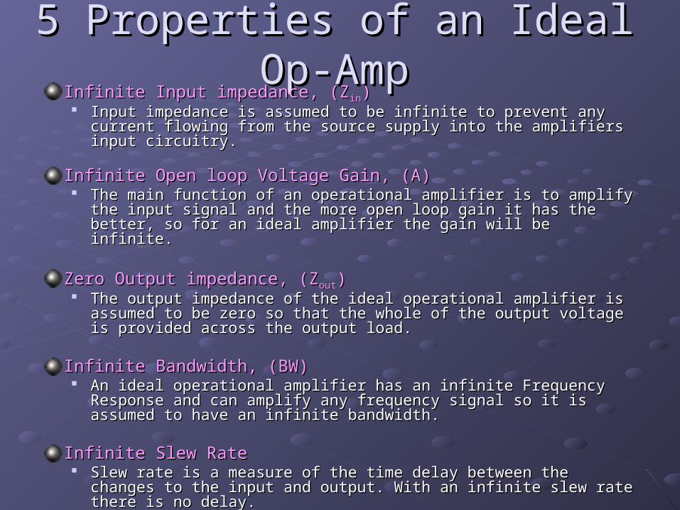
5 Properties of an Ideal Op-Amp5 Properties of an Ideal Op-AmpInfinite Input impedance, (ZInfinite Input impedance, (Z inin))
Input impedance is assumed to be infinite to prevent any current flowing Input impedance is assumed to be infinite to prevent any current flowing from the source supply into the amplifiers input circuitry.from the source supply into the amplifiers input circuitry.
Infinite Open loop Voltage Gain, (A) Infinite Open loop Voltage Gain, (A) The main function of an operational amplifier is to amplify the input The main function of an operational amplifier is to amplify the input
signal and the more open loop gain it has the better, so for an ideal signal and the more open loop gain it has the better, so for an ideal amplifier the gain will be infinite. amplifier the gain will be infinite.
Zero Output impedance, (ZZero Output impedance, (Zoutout)) The output impedance of the ideal operational amplifier is assumed to The output impedance of the ideal operational amplifier is assumed to
be zero so that the whole of the output voltage is provided across the be zero so that the whole of the output voltage is provided across the output load.output load.
Infinite Bandwidth, (BW)Infinite Bandwidth, (BW) An ideal operational amplifier has an infinite Frequency Response and An ideal operational amplifier has an infinite Frequency Response and
can amplify any frequency signal so it is assumed to have an infinite can amplify any frequency signal so it is assumed to have an infinite bandwidth.bandwidth.
Infinite Slew RateInfinite Slew Rate Slew rate is a measure of the time delay between the changes to the Slew rate is a measure of the time delay between the changes to the
input and output. With an infinite slew rate there is no delay. input and output. With an infinite slew rate there is no delay.

The Real Op-AmpThe Real Op-AmpInput impedance, (ZInput impedance, (Zinin))
The input impedance is not infinite but usually between 10The input impedance is not infinite but usually between 1066 and 10and 101212 . .
Open loop Voltage Gain, (A) Open loop Voltage Gain, (A) The open loop gain is not infinite but 10The open loop gain is not infinite but 1055 for constant voltages. for constant voltages.
Output impedance, (ZOutput impedance, (Zoutout)) The output impedance is not zero but 10The output impedance is not zero but 1022 ..
Bandwidth, (BW)Bandwidth, (BW) Bandwidth is not unlimited.Bandwidth is not unlimited.
Slew RateSlew Rate Slew rate is not infinite but 10 V Slew rate is not infinite but 10 V ss-1-1. .
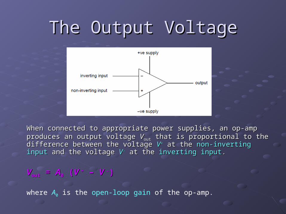
The Output VoltageThe Output Voltage
When connected to appropriate power supplies, an op-amp produces When connected to appropriate power supplies, an op-amp produces an output voltage an output voltage VVoutout that is proportional to the difference between that is proportional to the difference between the voltage the voltage VV++ at the at the non-inverting inputnon-inverting input and the voltage and the voltage VV-- at the at the inverting inputinverting input..
VVoutout = = AA00 ( (V V ++ – – V V ––))
where A0 is the open-loop gain of the op-amp.

The Power SupplyThe Power Supply
The common link between the two sets of batteries is termed the zero-volt, or earth, line. This forms the reference line from which all input and output voltages are measured. Connecting the supplies in this way enables the output voltage to be either positive or
negative.
The diagram shows an input V – connected to the inverting input and an input V + connected to the non-inverting input. The output voltage Vout of the op-amp is given by
VVoutout = = AA00 ( (V V ++ – – V V ––))
where A0 is the open-loop gain (typically 105 for d.c. voltages).

Example 1Example 1
Given: +ve supply line = +9.0 V –ve supply line = –9.0 V
V + = 1.4 V V – = 1.3 V
What is the output voltage? (What is the output voltage? (AA00 = 10 = 1055))
Solution:Solution:
VVoutout == AA00 ( (V V ++ – – V V ––) ) = 105 (1.4 – 1.3) = 10 000 VVVoutout == 9.0 V 9.0 V
This is not possible, the output voltage cannot exceed the power
supply voltage.The amplifier is said to be
saturated.Voutput = the power supply voltage
The amplifier is saturated.Voutput = the power supply voltageIn this case the output voltage is
negative.
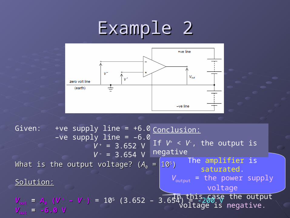
Example 2Example 2
Given: +ve supply line = +6.0 V –ve supply line = –6.0 V
V + = 3.652 V V – = 3.654 V
What is the output voltage? (What is the output voltage? (AA00 = 10 = 1055))
Solution:Solution:
VVoutout == AA00 ( (V V ++ – – V V ––) ) = 105 (3.652 – 3.654) = -200 VVVoutout == -6.0 V -6.0 V
Conclusion:
If V+ < V-, the output is negative

The amplifier is not saturated.
Example 3Example 3
Given: +ve supply line = +15.0 V –ve supply line = –15.0 V
V + = 0.9000 V V – = 0.8999 V
What is the output voltage? (What is the output voltage? (AA00 = 10 = 1055))
Solution:Solution:
VVoutout == AA00 ( (V V ++ – – V V ––) ) = 105 (0.9000 – 0.8999) = 10 VVVoutout == 10.0 V 10.0 V
Conclusion:
For the amplifier to be not saturated, the two inputs must be almost identical (same potential).

Example 4Example 4
The open-loop gain of an operational amplifier is The open-loop gain of an operational amplifier is 101055. If the supply is . If the supply is 9.0 V, what is the minimum 9.0 V, what is the minimum difference in input voltages that will cause the difference in input voltages that will cause the output to be saturated?output to be saturated?
Solution:Solution:
VVoutout == AA00 ( (V V ++ – – V V ––))((V V ++ – – V V ––) ) == VVout out / / AA0 0
== 9.0 / 10 9.0 / 105 5
== 9.0 × 10 9.0 × 1055 V V

Op-Amp as a ComparatorOp-Amp as a Comparator
It is usual to connect a potential divider to each of the two inputs. One potential divider provides a fixed voltage at one input while the other potential divider provides a voltage dependent on a sensor.
In the diagram, the resistors of resistance R will give rise to a constant voltage of ½VS at the inverting input. The LDR, of resistance RLDR is connected in series with a fixed resistor of resistance F.
If RRLDRLDR > > FF (that is, the LDR is in darkness), then V V ++ > > VV –– and the output is positiveoutput is positive. If RRLDRLDR < < FF (that is, the LDR is in daylight), then V V ++ < < V V –– and the output is negativeoutput is negative.
It can be seen that by suitable choice of the resistance F, the comparator gives an output, either positive or negative, that is dependent on light intensity. The light intensity at which the circuit switches polarity can be varied if the resistor of resistance F is replaced with a variable resistor.
The LDR could be replaced by other sensors to provide alternative sensing devices. For example, use of a thermistor could provide a frost-warning device.
The comparator is an open loop connection, there is no feedback from the output. So SoVVoutout = = AA00 ( (V V ++ – – V V ––)) applies

Example 5Example 5
The diagram shows a circuit incorporating an ideal operational amplifier (op-amp). The voltages applied to the inverting and the non-inverting inputs are V1 and V2 respectively.State the value of the output voltage VOUT when(a) V1 > V2 (b) V1 < V2
Solution:For an ideal operational amplifier, the gain is infinite and hence it is saturated.(a) When V1 > V2 V- > V+, therefore Vout is negative, Vout = -9 V(b) When V1 < V2 V+ > V-, therefore Vout is positive, Vout = +9 V
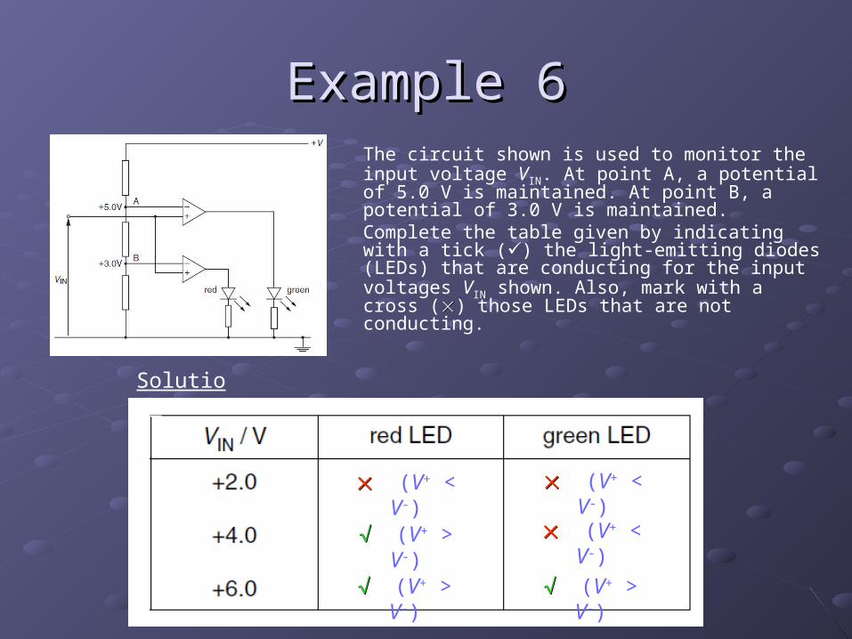
Example 6Example 6The circuit shown is used to monitor the input voltage VIN. At point A, a potential of 5.0 V is maintained. At point B, a potential of 3.0 V is maintained.Complete the table given by indicating with a tick ( ) the light-emitting diodes (LEDs) that are ✓conducting for the input voltages VIN shown. Also, mark with a cross () those LEDs that are not conducting.
(V+ > V-) (V+ > V-)
(V+ > V-) (V+ < V-)
(V+ < V-) (V+ < V-)
Solution:
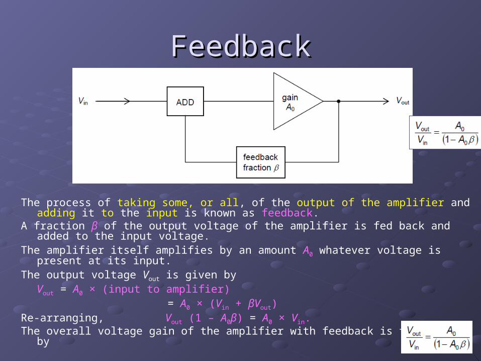
FeedbackFeedback
The process of taking some, or all, of the output of the amplifier and adding it to the input is known as feedback.
A fraction β of the output voltage of the amplifier is fed back and added to the input voltage.
The amplifier itself amplifies by an amount A0 whatever voltage is present at its input. The output voltage Vout is given by
Vout = A0 × (input to amplifier) = A0 × (Vin + βVout)
Re-arranging, Vout (1 – A0β) = A0 × Vin.The overall voltage gain of the amplifier with feedback is then given by

Negative FeedbackNegative Feedback
If the fraction β is negative denominator is greater than unity overall gain smaller than the open-loop gain A0
This can be achieved by feeding back part of the output to the inverting input. The reduction in amplification may bring the following benefits:
an increase in the range of frequencies over which the gain is constant (increased bandwidth), less distortion, greater operating stability.

The Inverting AmplifierThe Inverting Amplifier
At At V V ++, , VV = 0 (earth) = 0 (earth)To ensure amplifier is not saturated, To ensure amplifier is not saturated, V V V V ++
Therefore, at point P, Therefore, at point P, VV V V ++ 0 0 VIRTUAL EARTHVIRTUAL EARTH
If If VVinin is positive, current flows from input to output. is positive, current flows from input to output.
II at at V V is 0 since input impedance is is 0 since input impedance is ..Therefore: Therefore:
0 0
in f
in out
in f
in out
in f
fout
in in
I I
V V
R R
V V
R R
RV
V R
AA00The inverting amplifier inverts
the polarity of the output.Vout is rad out of phase with
the input voltage.
For inverting amplifier, Vin is fed into V .
The inverting amplifier is a negative feedback
connection.I
I

The Inverting AmplifierThe Inverting Amplifier
If the If the input is negativeinput is negative, current flows in the , current flows in the opposite directionopposite direction but it is but it is still the same current still the same current flowing through both Rflowing through both R inin and R and Rff..
0fout
in in
RVA
V R

Example 7 Example 7
The circuit shows an inverting amplifier. The input The circuit shows an inverting amplifier. The input voltage is 0.44 V. Calculate the output voltage.voltage is 0.44 V. Calculate the output voltage.
Solution:Solution:
VVoutout = = ((RRf f / / RRinin) × ) × VV = = (22 / 10) × 0.44(22 / 10) × 0.44 = = 0.968 V 0.968 V
10 k
22 k
Vin
Vo

Example 8Example 8
The diagram shows an inverting amplifier.The diagram shows an inverting amplifier.
Find its gain Find its gain AA00 and the output voltage and the output voltage VVoutout..
Solution:Solution:
A0 = ((RRf f / / RRinin) = ) = (10 / 2.0) = (10 / 2.0) = 55VVout out = = A0 × × VVin in = = 5.05.0 × 0.20× 0.20 = = 1.0 V1.0 V
2.0 k
10 k
Vout
Vin= 0.20 V
When Rf > Rin
A0 > 1 (increase)
When A0 > 1 Vout > Vin (increase)

Example 9Example 9
The diagram shows an amplifier circuit. The diagram shows an amplifier circuit. (a) What is its voltage gain(a) What is its voltage gain A A00??(b) What is the output voltage when the input voltage is (b) What is the output voltage when the input voltage is
(i) +0.5 V (i) +0.5 V (ii) -1.3 V (ii) -1.3 V ..
Solution:Solution:(a) A0 = ((RRf f / / RRinin) = ) = (10 / 2.0) = (10 / 2.0) = 22
(b) (i)(b) (i) V Vout out = = A0 × × VVin in = = 22 × 0.5× 0.5 = = 1.0 V1.0 V(ii)(ii) V Vout out = = A0 × × VVin in = = 22 × (× ( 1.3) 1.3) = +2.6 V= +2.6 V
5.0 k
10 k
Vout
Vin
When Vin is positive Vout is negative
When Vin is negative Vout is positive
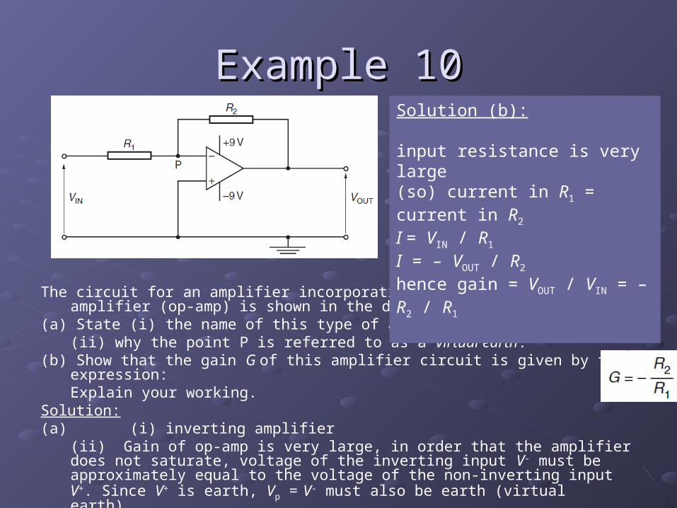
Example 10Example 10
The circuit for an amplifier incorporating an ideal operational amplifier (op-amp) is shown in the diagram.
(a) State (i) the name of this type of amplifier circuit, (ii) why the point P is referred to as a virtual earth.(b) Show that the gain G of this amplifier circuit is given by the expression: Explain your working.Solution:(a) (i) inverting amplifier
(ii) Gain of op-amp is very large, in order that the amplifier does not saturate, voltage of the inverting input V- must be approximately equal to the voltage of the non-inverting input V+. Since V+ is earth, Vp = V- must also be earth (virtual earth).
Solution (b):
input resistance is very large (so) current in R1 = current in R2 I = VIN / R1 I = – VOUT / R2 hence gain = VOUT / VIN = –R2 / R1
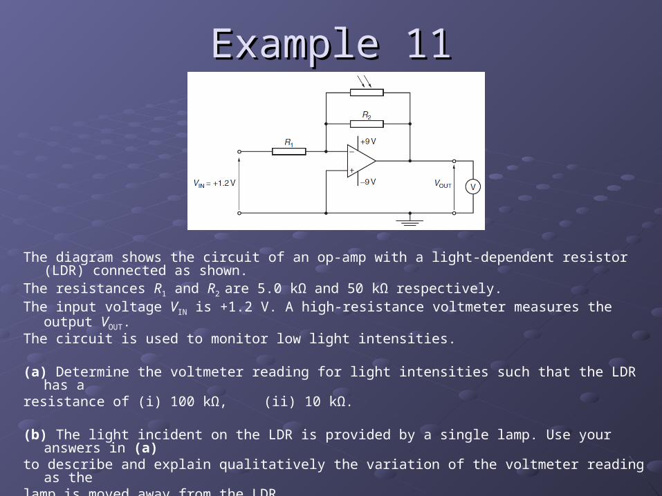
Example 11Example 11
The diagram shows the circuit of an op-amp with a light-dependent resistor (LDR) connected as shown.
The resistances R1 and R2 are 5.0 kΩ and 50 kΩ respectively.The input voltage VIN is +1.2 V. A high-resistance voltmeter measures the output VOUT.The circuit is used to monitor low light intensities.
(a) Determine the voltmeter reading for light intensities such that the LDR has aresistance of (i) 100 kΩ, (ii) 10 kΩ.
(b) The light incident on the LDR is provided by a single lamp. Use your answers in (a)to describe and explain qualitatively the variation of the voltmeter reading as thelamp is moved away from the LDR.

Solution 11Solution 11
Solution:
(a) The LDR is connected in parallel with R2
(i) feedback resistance, Rf = 33.3 kΩ gain, A0 = Rf / R1 = – 33.3 / 5 = – 6.66 VOUT = A0 × VIN = – 6.66 × 1.2 = – 8.0 V
(ii) feedback resistance, Rf = 8.33 kΩVOUT = A0 × VIN = –(8.33 / 5) × 1.2 = –2.0 V
(b) Moving the lamp away decreases the light intensityLDR resistance and feedback resistance increase Gain increases, voltmeter reading increases (Output voltage becomes more negative)

The Non-inverting AmplifierThe Non-inverting Amplifier
At At V V ++, , VV = = VVinin
To ensure amplifier is not saturated, To ensure amplifier is not saturated, V V V V + + VVinin
As As VVP P = = V V , , thereforetherefore V VP P = = VVin in
Current through RCurrent through R inin = Current through R = Current through R ff = = IIp.d. across Rp.d. across R inin and R and Rff: : VVoutout – 0 – 0 = = II ( (RRinin + + RRff))p.d. across Rp.d. across R inin: : VVpp – 0 = – 0 = I RI Rin in VVinin = = I RI Rinin
Therefore, Therefore, VVoutout / / VVinin = = ((RRinin + + RRff) / ) / RRinin
1 fout
in in
RV
V R AA00
Vin
I
I
The non-inverting amplifier:
• increases the output
• produces an output voltage that is in phase with the input voltage.
For non-inverting amplifier, Vin is fed into V +.
The non-inverting amplifier is a negative feedback connection.
VV

The Non-inverting AmplifierThe Non-inverting Amplifier
The formula for calculating The formula for calculating gain, gain, AA00 of a non-inverting of a non-inverting
amplifier can also be amplifier can also be derived using the potential derived using the potential divider rule:divider rule:
Remember Remember VVP P = = V V = = VVin in
Therefore, Therefore,
VVinin = [ = [RR11 / ( / (RRff + + RR11)] )] VVoutout
+
P
1 fout
in in
RV
V R
Equivalent Circuit:Equivalent Circuit:
AA00
Vin is fed into V + Vin is fed into V +

Example 12Example 12
The diagram shows a non-inverting amplifier circuit. Find The diagram shows a non-inverting amplifier circuit. Find its voltage gain its voltage gain AA00 and the output voltage. and the output voltage.
Solution:Solution:
A0 = 1 + (+ (RRf f / / RRinin) = 1 + (10 / 2.0) = 6) = 1 + (10 / 2.0) = 6
VVout out = = A0 × × VVin in = 6= 6 × 0.20× 0.20 = 1.2 V= 1.2 V
2.0 k
10 k
9VVin= 0.20 V
+9V
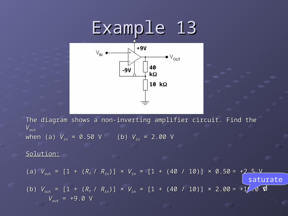
Example 13Example 13
The diagram shows a non-inverting amplifier circuit. Find the The diagram shows a non-inverting amplifier circuit. Find the VVoutout
when (a) when (a) VVinin = 0.50 V = 0.50 V (b) (b) VVinin = 2.00 V = 2.00 V
Solution:Solution:
(a) (a) VVoutout = [1 + ( = [1 + (RRf f / / RRinin)] × )] × VVinin = [1 + (40 / 10)] × 0.50 = [1 + (40 / 10)] × 0.50 = = +2.5 V +2.5 V
(b) (b) VVoutout = [1 + ( = [1 + (RRf f / / RRinin)] × )] × VVinin = [1 + (40 / 10)] × 2.00 = [1 + (40 / 10)] × 2.00 = = +10.0 V +10.0 V
VVoutout = +9.0 V = +9.0 V
10 k
40 k9V
+9V
saturated

Example 14Example 14
An amplifier circuit for a microphone is shown in the diagram.(a) Name the type of feedback used with this op-amp.(b) The output potential difference VOUT is 5.8 V for a potential difference across the
resistor R of 69 mV. Calculate(i) the gain of the amplifier circuit,(ii) the resistance of resistor X.
(c) State one effect on the amplifier output of reducing the resistance of resistor X.Solution:(a) Negative feedback (because part of the output is returned to the inverting input).(b) (i) Gain, A0 = Vout / Vin = 5.8 / (69 10-3) = 84 (ii) A0 = 1 + (Rf / R1); (Rf / R1) = 84 – 1 = 83; Rx = Rf / 83 = 120 / 83 = 1.45 k(c) When Rx is reduced, A0 increases and hence Vout increases.

Direct SensingDirect Sensing
A sensing device has a physical property changes with a change
in whatever it is monitoring.Example:
An LDR has its resistance change with light intensity.
The processing unit process the change in the physical property of the sensing device so that it can be indicated by the output device.
Example:The change in the resistance of the LDR is converted into a change in
voltage by a potential divider. The small voltage is amplified.
The output device indicate the change in
the monitored property.Example:
The output device switch on the lamp
when it is dark.

Sensing DevicesSensing Devices
An LDR has its resistance change with light intensity.A thermistor has its resistance change with temperature.A piezo-electric transducer has voltage produced according to sound pressure acting on it.A strain gauge has its resistance change with the strain acting on it.
(Read the notes given)

Output DevicesOutput Devices
The relayThe relay
The light-emitting diode (LED)The light-emitting diode (LED)
Digital and analogue meters as output Digital and analogue meters as output devices.devices.
(Read the notes given)(Read the notes given)

ExampleExample
A block diagram for an electronic sensor is shown in Fig. 9.1.(a) Complete Fig. 9.1 by labelling the remaining boxes.(b) A device is to be built that will emit a red light when its
input is at +2 V. When the input is at –2 V, the light emitted is to be green.(i) On Fig. 9.2, draw a circuit diagram of the device.(ii) Explain briefly the action of this device.

SolutionSolution
(a) blocks labelled sensing device / sensor / transducerprocessor / processing unit / signal conditioning
(b) (i) two LEDs with opposite polarities (ignore any series resistors) correctly identified as red and green
(ii) correct polarity for diode to conduct identified hence red LED conducts when input (+)ve or vice versa

Physics is Great!Physics is Great!
Enjoy Your Study!Enjoy Your Study!