Embed Size (px)
Citation preview

TMS320C62xxCPU and Instruction Set
Reference Guide
Literature Number: SPRU189BManufacturing Part Number: D426008-9761 revision A
July 1997
Printed on Recycled Paper

Running Title—Attribute Reference
ii
IMPORTANT NOTICE
Texas Instruments (TI) reserves the right to make changes to its products or to discontinue anysemiconductor product or service without notice, and advises its customers to obtain the latestversion of relevant information to verify, before placing orders, that the information being reliedon is current.
TI warrants performance of its semiconductor products and related software to the specificationsapplicable at the time of sale in accordance with TI’s standard warranty. Testing and other qualitycontrol techniques are utilized to the extent TI deems necessary to support this warranty.Specific testing of all parameters of each device is not necessarily performed, except thosemandated by government requirements.
Certain applications using semiconductor products may involve potential risks of death,personal injury, or severe property or environmental damage (“Critical Applications”).
TI SEMICONDUCTOR PRODUCTS ARE NOT DESIGNED, INTENDED, AUTHORIZED, ORWARRANTED TO BE SUITABLE FOR USE IN LIFE-SUPPORT APPLICATIONS, DEVICESOR SYSTEMS OR OTHER CRITICAL APPLICATIONS.
Inclusion of TI products in such applications is understood to be fully at the risk of the customer.Use of TI products in such applications requires the written approval of an appropriate TI officer.Questions concerning potential risk applications should be directed to TI through a local SCsales office.
In order to minimize risks associated with the customer’s applications, adequate design andoperating safeguards should be provided by the customer to minimize inherent or proceduralhazards.
TI assumes no liability for applications assistance, customer product design, softwareperformance, or infringement of patents or services described herein. Nor does TI warrant orrepresent that any license, either express or implied, is granted under any patent right, copyright,mask work right, or other intellectual property right of TI covering or relating to any combination,machine, or process in which such semiconductor products or services might be or are used.
Copyright 1997, Texas Instruments Incorporated

iii
Preface
Read This First
About This Manual
This reference guide describes the CPU architecture, pipeline, instruction set,and interrupts for the TMS320C62xx digital signal processors (DSPs). Unlessotherwise specified, all references to the ’C6x refer to the TMS320C6x genera-tion of DSPs and ’C62xx refer to the TMS320C62xx DSPs in the ’C6x genera-tion.
How to Use This Manual
Use this manual as a reference for the architecture of the TMS320C62xx CPU.First-time readers should read Chapter 1 for general information about TIDSPs, the features of the TMS320C62xx, and the applications for which theTMS320C62xx is best suited.
Read chapters 2, 4, and 5 to grasp the concepts of the architecture.Chapter 3 contains detailed information about each instruction and is bestused as reference material; however, you may want to read sections 3.1through 3.8 for general information about the instruction set and to understandthe instruction descriptions, then browse through Chapter 3 to familiarize your-self with the instructions.
The following table gives chapter references for specific information:
If you are looking for in-formation about: Turn to these chapters:
Addressing modes Chapter 3, Instruction Set
Conditional operations Chapter 3, Instruction Set
Control registers Chapter 2, CPU Overview
CPU architecture Chapter 2, CPU Overview
CPU data paths Chapter 2, CPU Overview
Delay slots Chapter 3, Instruction Set
Chapter 4, Pipeline Operation

Notational Conventions
iv
If you are looking for in-formation about: Turn to these chapters:
General-purpose register files Chapter 2, CPU Overview
Instruction set Chapter 3, Instruction Set
Interrupt control registers Chapter 5, Interrupts
Interrupts Chapter 5, Interrupts
Parallel operations Chapter 3, Instruction Set
Pipeline operation Chapter 4, Pipeline Operation
Pipeline phases Chapter 4, Pipeline Operation
Reset Chapter 5, Interrupts
If you are interested in topics that are not listed here, check Related Documen-tation From Texas Instruments, page v, for brief descriptions of other’C62xx-related books that are available.
Notational Conventions
This document uses the following conventions:
� Program listings and program examples are shown in a special font .Here is a sample program listing:
LDW .D1 *A0,A1ADD .L1 A1,A2,A3NOP 3MPY .M1 A1,A4,A5
� To help you easily recognize instructions and parameters throughout thebook, instructions are in bold face and parameters are in italics (exceptin program listings).
� In instruction syntaxes, portions of a syntax that are in bold should be en-tered as shown; portions of a syntax that are in italics describe the type ofinformation that should be entered. Here is an example of an instruction:
MPY src1,src2,dst
MPY is the instruction mnemonic. When you use MPY, you must supplytwo source operands (src1 and src2) and a destination operand (dst) ofappropriate types as defined in Chapter 3, Instruction Set.
Although the instruction mnemonic (MPY in this example) is in capital let-ters, the ’C6x assembler is not case sensitive — it can assemble mnemon-ics entered in either upper or lower case.
How to Use This Manual/Notational Conventions

Related Documentation From Texas Instruments
v Read This First
� Square brackets, [ and ], and parentheses, ( and ), are used to identify op-tional items. If you use an optional item, you must specify the informationwithin brackets or parentheses; however, you do not enter the brackets orparentheses themselves. Here is an example of an instruction that has op-tional items.
[label] EXTU (.unit) src2, csta, cstb, dst
The EXTU instruction is shown with a label and several parameters. The[label] and the parameter (.unit) are optional. The parameters src2, csta,cstb, and dst are not optional.
� Throughout this book MSB means most significant bit and LSB meansleast significant bit.
Related Documentation From Texas Instruments
The following books describe the TMS320C6x generation and related supporttools. To obtain a copy of any of these TI documents, call the Texas Instru-ments Literature Response Center at (800) 477–8924. When ordering, pleaseidentify the book by its title and literature number.
TMS320C62xx Technical Brief (literature number SPRU197) gives anintroduction to the ’C62xx digital signal processor, development tools,and third-party support.
TMS320C62xx Peripherals Reference Guide (literature number SPRU190)describes common peripherals available on the TMS320C62xx digitalsignal processors. This book includes information on the internal dataand program memories, the external memory interface (EMIF), the hostport, serial ports, direct memory access (DMA), clocking and phase-locked loop (PLL), and the power-down modes.
TMS320C62xx Programmer’s Guide (literature number SPRU198)describes ways to optimize C and assembly code and includes applica-tion program examples.
TMS320C6x Assembly Language Tools User’s Guide (literature numberSPRU186) describes the assembly language tools (assembler, linker,and other tools used to develop assembly language code), assemblerdirectives, macros, common object file format, and symbolic debuggingdirectives for the ’C6x generation of devices.
TMS320C6x Optimizing C Compiler User’s Guide (literature numberSPRU187) describes the ’C6x C compiler. This C compiler accepts ANSIstandard C source code and produces assembly language source codefor the ’C6x generation of devices. This book also describes theassembly optimizer, which helps you optimize your assembly code.
Notational Conventions/Related Documentation From Texas Instruments

Trademarks
vi
TMS320C6x C Source Debugger User’s Guide (literature numberSPRU188) tells you how to invoke the ’C6x simulator and emulatorversions of the C source debugger interface. This book discussesvarious aspects of the debugger, including command entry, codeexecution, data management, breakpoints, profiling, and analysis.
TMS320 Third-Party Support Reference Guide (literature numberSPRU052) alphabetically lists over 100 third parties that provide variousproducts that serve the family of TMS320 digital signal processors. Amyriad of products and applications are offered—software and hardwaredevelopment tools, speech recognition, image processing, noise can-cellation, modems, etc.
TMS320C6201 Digital Signal Processor Data Sheet (literature numberSPRS051) describes the features of the TMS320C6xx and provides pin-outs, electrical specifications, and timings for the device.
Trademarks
XDS510, VelociTI, and 320 Hotline On-line are trademarks of Texas Instru-ments Incorporated.
Windows and Windows NT are registered trademarks of Microsoft Corpora-tion.
Related Documentation From Texas Instruments/Trademarks
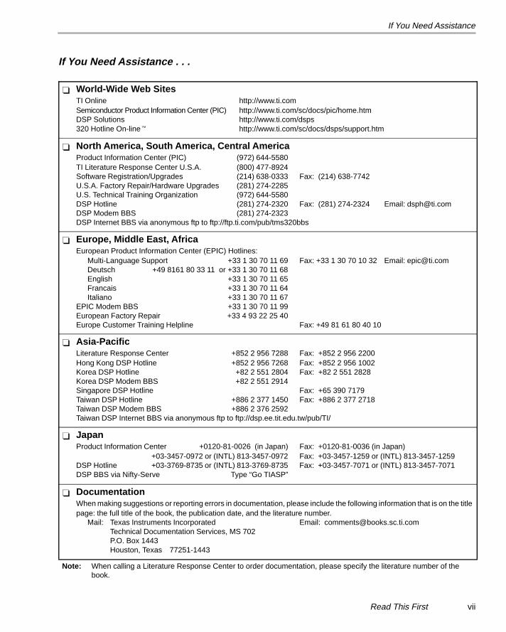
If You Need Assistance
vii Read This First
If You Need Assistance . . .
� World-Wide Web SitesTI Online http://www.ti.comSemiconductor Product Information Center (PIC) http://www.ti.com/sc/docs/pic/home.htmDSP Solutions http://www.ti.com/dsps320 Hotline On-line� http://www.ti.com/sc/docs/dsps/support.htm
� North America, South America, Central AmericaProduct Information Center (PIC) (972) 644-5580TI Literature Response Center U.S.A. (800) 477-8924Software Registration/Upgrades (214) 638-0333 Fax: (214) 638-7742U.S.A. Factory Repair/Hardware Upgrades (281) 274-2285U.S. Technical Training Organization (972) 644-5580DSP Hotline (281) 274-2320 Fax: (281) 274-2324 Email: [email protected] Modem BBS (281) 274-2323DSP Internet BBS via anonymous ftp to ftp://ftp.ti.com/pub/tms320bbs
� Europe, Middle East, AfricaEuropean Product Information Center (EPIC) Hotlines:
Multi-Language Support +33 1 30 70 11 69 Fax: +33 1 30 70 10 32 Email: [email protected] +49 8161 80 33 11 or +33 1 30 70 11 68English +33 1 30 70 11 65Francais +33 1 30 70 11 64Italiano +33 1 30 70 11 67
EPIC Modem BBS +33 1 30 70 11 99European Factory Repair +33 4 93 22 25 40Europe Customer Training Helpline Fax: +49 81 61 80 40 10
� Asia-PacificLiterature Response Center +852 2 956 7288 Fax: +852 2 956 2200Hong Kong DSP Hotline +852 2 956 7268 Fax: +852 2 956 1002Korea DSP Hotline +82 2 551 2804 Fax: +82 2 551 2828Korea DSP Modem BBS +82 2 551 2914Singapore DSP Hotline Fax: +65 390 7179Taiwan DSP Hotline +886 2 377 1450 Fax: +886 2 377 2718Taiwan DSP Modem BBS +886 2 376 2592Taiwan DSP Internet BBS via anonymous ftp to ftp://dsp.ee.tit.edu.tw/pub/TI/
� JapanProduct Information Center +0120-81-0026 (in Japan) Fax: +0120-81-0036 (in Japan)
+03-3457-0972 or (INTL) 813-3457-0972 Fax: +03-3457-1259 or (INTL) 813-3457-1259DSP Hotline +03-3769-8735 or (INTL) 813-3769-8735 Fax: +03-3457-7071 or (INTL) 813-3457-7071DSP BBS via Nifty-Serve Type “Go TIASP”
� DocumentationWhen making suggestions or reporting errors in documentation, please include the following information that is on the titlepage: the full title of the book, the publication date, and the literature number.
Mail: Texas Instruments Incorporated Email: [email protected] Documentation Services, MS 702P.O. Box 1443Houston, Texas 77251-1443
Note: When calling a Literature Response Center to order documentation, please specify the literature number of thebook.

Contents
ix
Contents
1 Introduction 1-1. . . . . . . . . . . . . . . . . . . . . . . . . . . . . . . . . . . . . . . . . . . . . . . . . . . . . . . . . . . . . . . . . . . . . Summarizes the features of the TMS320 family of products and presents typical applications.Describes the TMS320C62xx DSP and lists its key features.
1.1 TMS320 Family Overview 1-2. . . . . . . . . . . . . . . . . . . . . . . . . . . . . . . . . . . . . . . . . . . . . . . . . . . 1.1.1 History of TMS320 DSPs 1-2. . . . . . . . . . . . . . . . . . . . . . . . . . . . . . . . . . . . . . . . . . . . . 1.1.2 Typical Applications for the TMS320 Family 1-2. . . . . . . . . . . . . . . . . . . . . . . . . . . . .
1.2 Overview of the TMS320C6x Generation of Digital Signal Processors 1-4. . . . . . . . . . . . . 1.3 Features and Options of the TMS320C62xx 1-4. . . . . . . . . . . . . . . . . . . . . . . . . . . . . . . . . . . . 1.4 TMS320C62xx Architecture 1-6. . . . . . . . . . . . . . . . . . . . . . . . . . . . . . . . . . . . . . . . . . . . . . . . . .
1.4.1 Central Processing Unit (CPU) 1-7. . . . . . . . . . . . . . . . . . . . . . . . . . . . . . . . . . . . . . . . 1.4.2 Internal Memory 1-8. . . . . . . . . . . . . . . . . . . . . . . . . . . . . . . . . . . . . . . . . . . . . . . . . . . . . 1.4.3 Peripherals 1-8. . . . . . . . . . . . . . . . . . . . . . . . . . . . . . . . . . . . . . . . . . . . . . . . . . . . . . . . .
2 CPU Data Paths and Control 2-1. . . . . . . . . . . . . . . . . . . . . . . . . . . . . . . . . . . . . . . . . . . . . . . . . . . . . Summarizes the TMS320C62xx architecture and describes the primary components of theCPU.
2.1 CPU Data Paths 2-2. . . . . . . . . . . . . . . . . . . . . . . . . . . . . . . . . . . . . . . . . . . . . . . . . . . . . . . . . . . . 2.1.1 General-Purpose Register Files 2-2. . . . . . . . . . . . . . . . . . . . . . . . . . . . . . . . . . . . . . . 2.1.2 Functional Units 2-3. . . . . . . . . . . . . . . . . . . . . . . . . . . . . . . . . . . . . . . . . . . . . . . . . . . . . 2.1.3 Register File Cross Paths 2-5. . . . . . . . . . . . . . . . . . . . . . . . . . . . . . . . . . . . . . . . . . . . . 2.1.4 Memory, Load, and Store Paths 2-5. . . . . . . . . . . . . . . . . . . . . . . . . . . . . . . . . . . . . . . 2.1.5 Data Address Paths 2-5. . . . . . . . . . . . . . . . . . . . . . . . . . . . . . . . . . . . . . . . . . . . . . . . .
2.2 Control Register File 2-6. . . . . . . . . . . . . . . . . . . . . . . . . . . . . . . . . . . . . . . . . . . . . . . . . . . . . . . . 2.3 Addressing Mode Register (AMR) 2-7. . . . . . . . . . . . . . . . . . . . . . . . . . . . . . . . . . . . . . . . . . . . 2.4 Control Status Register (CSR) 2-9. . . . . . . . . . . . . . . . . . . . . . . . . . . . . . . . . . . . . . . . . . . . . . . .
3 Instruction Set 3-1. . . . . . . . . . . . . . . . . . . . . . . . . . . . . . . . . . . . . . . . . . . . . . . . . . . . . . . . . . . . . . . . . . Describes the TMS320C62xx instruction set, including examples of each instruction. Providesinformation about addressing modes, resource constraints, parallel operations, and conditionaloperations.
3.1 Instruction Operation and Execution Notations 3-2. . . . . . . . . . . . . . . . . . . . . . . . . . . . . . . . . . 3.2 Mapping Between Instructions and Functional Units 3-4. . . . . . . . . . . . . . . . . . . . . . . . . . . . . 3.3 TMS320C62xx Opcode Map 3-7. . . . . . . . . . . . . . . . . . . . . . . . . . . . . . . . . . . . . . . . . . . . . . . . . 3.4 Delay Slots 3-9. . . . . . . . . . . . . . . . . . . . . . . . . . . . . . . . . . . . . . . . . . . . . . . . . . . . . . . . . . . . . . . . 3.5 Parallel Operations 3-10. . . . . . . . . . . . . . . . . . . . . . . . . . . . . . . . . . . . . . . . . . . . . . . . . . . . . . . .

Contents
x
3.5.1 Example Parallel Code 3-12. . . . . . . . . . . . . . . . . . . . . . . . . . . . . . . . . . . . . . . . . . . . . . 3.5.2 Branching Into the Middle of an Execute Packet 3-12. . . . . . . . . . . . . . . . . . . . . . . .
3.6 Conditional Operations 3-13. . . . . . . . . . . . . . . . . . . . . . . . . . . . . . . . . . . . . . . . . . . . . . . . . . . . . 3.7 Resource Constraints 3-14. . . . . . . . . . . . . . . . . . . . . . . . . . . . . . . . . . . . . . . . . . . . . . . . . . . . . .
3.7.1 Constraints on Instructions Using the Same Functional Unit 3-14. . . . . . . . . . . . . . 3.7.2 Constraints on Cross Paths (1X and 2X) 3-14. . . . . . . . . . . . . . . . . . . . . . . . . . . . . . . 3.7.3 Constraints on Loads and Stores 3-15. . . . . . . . . . . . . . . . . . . . . . . . . . . . . . . . . . . . . 3.7.4 Constraints on Long (40-Bit) Data 3-15. . . . . . . . . . . . . . . . . . . . . . . . . . . . . . . . . . . . 3.7.5 Constraints on Register Reads 3-16. . . . . . . . . . . . . . . . . . . . . . . . . . . . . . . . . . . . . . . 3.7.6 Constraints on Register Writes 3-16. . . . . . . . . . . . . . . . . . . . . . . . . . . . . . . . . . . . . . .
3.8 Addressing Modes 3-18. . . . . . . . . . . . . . . . . . . . . . . . . . . . . . . . . . . . . . . . . . . . . . . . . . . . . . . . . 3.8.1 Linear Addressing Mode 3-18. . . . . . . . . . . . . . . . . . . . . . . . . . . . . . . . . . . . . . . . . . . . . 3.8.2 Circular Addressing Mode 3-18. . . . . . . . . . . . . . . . . . . . . . . . . . . . . . . . . . . . . . . . . . . 3.8.3 Syntax for Load/Store Address Generation 3-20. . . . . . . . . . . . . . . . . . . . . . . . . . . .
3.9 Individual Instruction Descriptions 3-21. . . . . . . . . . . . . . . . . . . . . . . . . . . . . . . . . . . . . . . . . . . .
4 TMS320C62xx Pipeline 4-1. . . . . . . . . . . . . . . . . . . . . . . . . . . . . . . . . . . . . . . . . . . . . . . . . . . . . . . . . . Describes pipeline phases, pipeline operation, and pipeline discontinuities for theTMS320C62xx CPU pipeline.
4.1 Pipeline Operation Overview 4-2. . . . . . . . . . . . . . . . . . . . . . . . . . . . . . . . . . . . . . . . . . . . . . . . . 4.1.1 Fetch 4-3. . . . . . . . . . . . . . . . . . . . . . . . . . . . . . . . . . . . . . . . . . . . . . . . . . . . . . . . . . . . . . 4.1.2 Decode 4-4. . . . . . . . . . . . . . . . . . . . . . . . . . . . . . . . . . . . . . . . . . . . . . . . . . . . . . . . . . . . 4.1.3 Execute 4-5. . . . . . . . . . . . . . . . . . . . . . . . . . . . . . . . . . . . . . . . . . . . . . . . . . . . . . . . . . . . 4.1.4 Summary of Pipeline Operation 4-6. . . . . . . . . . . . . . . . . . . . . . . . . . . . . . . . . . . . . . .
4.2 Pipeline Execution of Instruction Types 4-10. . . . . . . . . . . . . . . . . . . . . . . . . . . . . . . . . . . . . . . 4.2.1 Single-Cycle Instructions 4-11. . . . . . . . . . . . . . . . . . . . . . . . . . . . . . . . . . . . . . . . . . . . 4.2.2 Multiply Instructions 4-11. . . . . . . . . . . . . . . . . . . . . . . . . . . . . . . . . . . . . . . . . . . . . . . . . 4.2.3 Store Instructions 4-12. . . . . . . . . . . . . . . . . . . . . . . . . . . . . . . . . . . . . . . . . . . . . . . . . . . 4.2.4 Load Instructions 4-14. . . . . . . . . . . . . . . . . . . . . . . . . . . . . . . . . . . . . . . . . . . . . . . . . . . 4.2.5 Branch Instructions 4-15. . . . . . . . . . . . . . . . . . . . . . . . . . . . . . . . . . . . . . . . . . . . . . . . .
4.3 Performance Considerations 4-17. . . . . . . . . . . . . . . . . . . . . . . . . . . . . . . . . . . . . . . . . . . . . . . . 4.3.1 Pipeline Operation With Multiple Execute Packets in a Fetch Packet 4-17. . . . . . 4.3.2 Multicycle NOPs 4-18. . . . . . . . . . . . . . . . . . . . . . . . . . . . . . . . . . . . . . . . . . . . . . . . . . . . 4.3.3 Memory Considerations 4-21. . . . . . . . . . . . . . . . . . . . . . . . . . . . . . . . . . . . . . . . . . . . .
5 Interrupts 5-1. . . . . . . . . . . . . . . . . . . . . . . . . . . . . . . . . . . . . . . . . . . . . . . . . . . . . . . . . . . . . . . . . . . . . . . Describes the TMS320C62xx interrupts, including reset and nonmaskable interrupts (NMI) andexplains interrupt control, detection, and processing.
5.1 Overview of Interrupts 5-2. . . . . . . . . . . . . . . . . . . . . . . . . . . . . . . . . . . . . . . . . . . . . . . . . . . . . . . 5.1.1 Types of Interrupts and Signals Used 5-2. . . . . . . . . . . . . . . . . . . . . . . . . . . . . . . . . . 5.1.2 Interrupt Service Table (IST) 5-5. . . . . . . . . . . . . . . . . . . . . . . . . . . . . . . . . . . . . . . . . . 5.1.3 Summary of Interrupt Control Registers 5-10. . . . . . . . . . . . . . . . . . . . . . . . . . . . . . .
5.2 Globally Enabling and Disabling Interrupts (Control Status Register–CSR) 5-11. . . . . . . . . . . . . . . . . . . . . . . . . . . . . . . . . . . . . . . . . . . . . .

Contents
xi Contents
5.3 Individual Interrupt Control 5-13. . . . . . . . . . . . . . . . . . . . . . . . . . . . . . . . . . . . . . . . . . . . . . . . . . 5.3.1 Enabling and Disabling Interrupts (Interrupt Enable Register–IER) 5-13. . . . . . . . 5.3.2 Status of, Setting, and Clearing Interrupts
(Interrupt Flag, Set, and Clear Registers – IFR, ISR, ICR) 5-14. . . . . . . . . . . . . . . . 5.3.3 Returning From Interrupt Servicing 5-16. . . . . . . . . . . . . . . . . . . . . . . . . . . . . . . . . . .
5.4 Interrupt Detection and Processing 5-18. . . . . . . . . . . . . . . . . . . . . . . . . . . . . . . . . . . . . . . . . . . 5.4.1 Setting the Interrupt Flag – Nonreset 5-18. . . . . . . . . . . . . . . . . . . . . . . . . . . . . . . . . . 5.4.2 Conditions for Processing an Interrupt – Nonreset 5-18. . . . . . . . . . . . . . . . . . . . . . 5.4.3 Actions Taken During Interrupt Processing – Nonreset 5-20. . . . . . . . . . . . . . . . . . 5.4.4 Setting the Interrupt Flag – RESET 5-21. . . . . . . . . . . . . . . . . . . . . . . . . . . . . . . . . . . 5.4.5 Actions Taken During Interrupt Processing – RESET 5-22. . . . . . . . . . . . . . . . . . . .
5.5 Performance Considerations 5-23. . . . . . . . . . . . . . . . . . . . . . . . . . . . . . . . . . . . . . . . . . . . . . . . 5.5.1 General Performance 5-23. . . . . . . . . . . . . . . . . . . . . . . . . . . . . . . . . . . . . . . . . . . . . . . 5.5.2 Pipeline Interaction 5-23. . . . . . . . . . . . . . . . . . . . . . . . . . . . . . . . . . . . . . . . . . . . . . . . .
5.6 Programming Considerations 5-24. . . . . . . . . . . . . . . . . . . . . . . . . . . . . . . . . . . . . . . . . . . . . . . 5.6.1 Single Assignment Programming 5-24. . . . . . . . . . . . . . . . . . . . . . . . . . . . . . . . . . . . . 5.6.2 Nested Interrupts 5-25. . . . . . . . . . . . . . . . . . . . . . . . . . . . . . . . . . . . . . . . . . . . . . . . . . . 5.6.3 Manual Interrupt Processing 5-25. . . . . . . . . . . . . . . . . . . . . . . . . . . . . . . . . . . . . . . . . 5.6.4 Traps 5-26. . . . . . . . . . . . . . . . . . . . . . . . . . . . . . . . . . . . . . . . . . . . . . . . . . . . . . . . . . . . .
A Glossary A-1. . . . . . . . . . . . . . . . . . . . . . . . . . . . . . . . . . . . . . . . . . . . . . . . . . . . . . . . . . . . . . . . . . . . . . . . Defines terms and abbreviations used throughout this book.
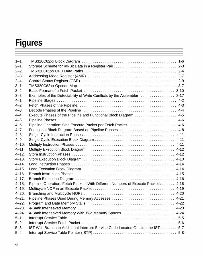
Figures
xii
Figures
1–1. TMS320C62xx Block Diagram 1-6. . . . . . . . . . . . . . . . . . . . . . . . . . . . . . . . . . . . . . . . . . . . . . . . . . 2–1. Storage Scheme for 40-Bit Data in a Register Pair 2-3. . . . . . . . . . . . . . . . . . . . . . . . . . . . . . . . . 2–2. TMS320C62xx CPU Data Paths 2-4. . . . . . . . . . . . . . . . . . . . . . . . . . . . . . . . . . . . . . . . . . . . . . . . 2–3. Addressing Mode Register (AMR) 2-7. . . . . . . . . . . . . . . . . . . . . . . . . . . . . . . . . . . . . . . . . . . . . . . 2–4. Control Status Register (CSR) 2-9. . . . . . . . . . . . . . . . . . . . . . . . . . . . . . . . . . . . . . . . . . . . . . . . . . 3–1. TMS320C62xx Opcode Map 3-7. . . . . . . . . . . . . . . . . . . . . . . . . . . . . . . . . . . . . . . . . . . . . . . . . . . . 3–2. Basic Format of a Fetch Packet 3-10. . . . . . . . . . . . . . . . . . . . . . . . . . . . . . . . . . . . . . . . . . . . . . . . 3–3. Examples of the Detectability of Write Conflicts by the Assembler 3-17. . . . . . . . . . . . . . . . . . 4–1. Pipeline Stages 4-2. . . . . . . . . . . . . . . . . . . . . . . . . . . . . . . . . . . . . . . . . . . . . . . . . . . . . . . . . . . . . . . 4–2. Fetch Phases of the Pipeline 4-3. . . . . . . . . . . . . . . . . . . . . . . . . . . . . . . . . . . . . . . . . . . . . . . . . . . 4–3. Decode Phases of the Pipeline 4-4. . . . . . . . . . . . . . . . . . . . . . . . . . . . . . . . . . . . . . . . . . . . . . . . . 4–4. Execute Phases of the Pipeline and Functional Block Diagram 4-5. . . . . . . . . . . . . . . . . . . . . . 4–5. Pipeline Phases 4-6. . . . . . . . . . . . . . . . . . . . . . . . . . . . . . . . . . . . . . . . . . . . . . . . . . . . . . . . . . . . . . 4–6. Pipeline Operation: One Execute Packet per Fetch Packet 4-6. . . . . . . . . . . . . . . . . . . . . . . . . 4–7. Functional Block Diagram Based on Pipeline Phases 4-8. . . . . . . . . . . . . . . . . . . . . . . . . . . . . . 4–8. Single-Cycle Instruction Phases 4-11. . . . . . . . . . . . . . . . . . . . . . . . . . . . . . . . . . . . . . . . . . . . . . . . 4–9. Single-Cycle Execution Block Diagram 4-11. . . . . . . . . . . . . . . . . . . . . . . . . . . . . . . . . . . . . . . . . . 4–10. Multiply Instruction Phases 4-11. . . . . . . . . . . . . . . . . . . . . . . . . . . . . . . . . . . . . . . . . . . . . . . . . . . . 4–11. Multiply Execution Block Diagram 4-12. . . . . . . . . . . . . . . . . . . . . . . . . . . . . . . . . . . . . . . . . . . . . . 4–12. Store Instruction Phases 4-12. . . . . . . . . . . . . . . . . . . . . . . . . . . . . . . . . . . . . . . . . . . . . . . . . . . . . . 4–13. Store Execution Block Diagram 4-13. . . . . . . . . . . . . . . . . . . . . . . . . . . . . . . . . . . . . . . . . . . . . . . . 4–14. Load Instruction Phases 4-14. . . . . . . . . . . . . . . . . . . . . . . . . . . . . . . . . . . . . . . . . . . . . . . . . . . . . . 4–15. Load Execution Block Diagram 4-14. . . . . . . . . . . . . . . . . . . . . . . . . . . . . . . . . . . . . . . . . . . . . . . . 4–16. Branch Instruction Phases 4-15. . . . . . . . . . . . . . . . . . . . . . . . . . . . . . . . . . . . . . . . . . . . . . . . . . . . 4–17. Branch Execution Diagram 4-16. . . . . . . . . . . . . . . . . . . . . . . . . . . . . . . . . . . . . . . . . . . . . . . . . . . . 4–18. Pipeline Operation: Fetch Packets With Different Numbers of Execute Packets 4-18. . . . . . . 4–19. Multicycle NOP in an Execute Packet 4-19. . . . . . . . . . . . . . . . . . . . . . . . . . . . . . . . . . . . . . . . . . . 4–20. Branching and Multicycle NOPs 4-20. . . . . . . . . . . . . . . . . . . . . . . . . . . . . . . . . . . . . . . . . . . . . . . . 4–21. Pipeline Phases Used During Memory Accesses 4-21. . . . . . . . . . . . . . . . . . . . . . . . . . . . . . . . . 4–22. Program and Data Memory Stalls 4-22. . . . . . . . . . . . . . . . . . . . . . . . . . . . . . . . . . . . . . . . . . . . . . 4–23. 4-Bank Interleaved Memory 4-23. . . . . . . . . . . . . . . . . . . . . . . . . . . . . . . . . . . . . . . . . . . . . . . . . . . 4–24. 4-Bank Interleaved Memory With Two Memory Spaces 4-24. . . . . . . . . . . . . . . . . . . . . . . . . . . 5–1. Interrupt Service Table 5-5. . . . . . . . . . . . . . . . . . . . . . . . . . . . . . . . . . . . . . . . . . . . . . . . . . . . . . . . . 5–2. Interrupt Service Fetch Packet 5-6. . . . . . . . . . . . . . . . . . . . . . . . . . . . . . . . . . . . . . . . . . . . . . . . . . 5–3. IST With Branch to Additional Interrupt Service Code Located Outside the IST 5-7. . . . . . . . 5–4. Interrupt Service Table Pointer (ISTP) 5-8. . . . . . . . . . . . . . . . . . . . . . . . . . . . . . . . . . . . . . . . . . . .

Figures
xiii Contents
5–5. Control Status Register (CSR) 5-11. . . . . . . . . . . . . . . . . . . . . . . . . . . . . . . . . . . . . . . . . . . . . . . . . 5–6. Interrupt Enable Register (IER) 5-13. . . . . . . . . . . . . . . . . . . . . . . . . . . . . . . . . . . . . . . . . . . . . . . . 5–7. Interrupt Flag Register (IFR) 5-14. . . . . . . . . . . . . . . . . . . . . . . . . . . . . . . . . . . . . . . . . . . . . . . . . . . 5–8. Interrupt Set Register (ISR) 5-15. . . . . . . . . . . . . . . . . . . . . . . . . . . . . . . . . . . . . . . . . . . . . . . . . . . . 5–9. Interrupt Clear Register (ICR) 5-15. . . . . . . . . . . . . . . . . . . . . . . . . . . . . . . . . . . . . . . . . . . . . . . . . . 5–10. NMI Return Pointer (NRP) 5-16. . . . . . . . . . . . . . . . . . . . . . . . . . . . . . . . . . . . . . . . . . . . . . . . . . . . . 5–11. Interrupt Return Pointer (IRP) 5-17. . . . . . . . . . . . . . . . . . . . . . . . . . . . . . . . . . . . . . . . . . . . . . . . . . 5–12. Interrupt Detection and Processing: Pipeline Operation–Nonreset 5-19. . . . . . . . . . . . . . . . . . 5–13. Interrupt Detection and Processing: Pipeline Operation–RESET 5-21. . . . . . . . . . . . . . . . . . . .

Tables
xiv
Tables
1–1. Typical Applications for the TMS320 DSPs 1-3. . . . . . . . . . . . . . . . . . . . . . . . . . . . . . . . . . . . . . . 2–1. Long (40-Bit) Register Pairs 2-2. . . . . . . . . . . . . . . . . . . . . . . . . . . . . . . . . . . . . . . . . . . . . . . . . . . . 2–2. Functional Units and Operations Performed 2-3. . . . . . . . . . . . . . . . . . . . . . . . . . . . . . . . . . . . . . 2–3. Control Registers 2-6. . . . . . . . . . . . . . . . . . . . . . . . . . . . . . . . . . . . . . . . . . . . . . . . . . . . . . . . . . . . . 2–4. Addressing Mode Field Encoding 2-7. . . . . . . . . . . . . . . . . . . . . . . . . . . . . . . . . . . . . . . . . . . . . . . 2–5. Block Size Calculations 2-8. . . . . . . . . . . . . . . . . . . . . . . . . . . . . . . . . . . . . . . . . . . . . . . . . . . . . . . . 2–6. Control Status Register: Fields, Read/Write Status, and Function 2-9. . . . . . . . . . . . . . . . . . . . 3–1. Instruction Operation and Execution Notations 3-2. . . . . . . . . . . . . . . . . . . . . . . . . . . . . . . . . . . . 3–2. Instruction to Functional Unit Mapping 3-4. . . . . . . . . . . . . . . . . . . . . . . . . . . . . . . . . . . . . . . . . . . 3–3. Functional Unit to Instruction Mapping 3-5. . . . . . . . . . . . . . . . . . . . . . . . . . . . . . . . . . . . . . . . . . . 3–4. Delay Slot Summary 3-9. . . . . . . . . . . . . . . . . . . . . . . . . . . . . . . . . . . . . . . . . . . . . . . . . . . . . . . . . . . 3–5. Registers That Can Be Tested by Conditional Operations 3-13. . . . . . . . . . . . . . . . . . . . . . . . . 3–6. Indirect Address Generation for Load/Store 3-20. . . . . . . . . . . . . . . . . . . . . . . . . . . . . . . . . . . . . . 3–7. Relationships Between Operands, Operand Size, Signed/Unsigned,
Functional Units, and Opfields for Example Instruction (ADD Instruction) 3-23. . . . . . . . . . . . 3–8. Program Counter Values for Branch Using a Displacement Example 3-35. . . . . . . . . . . . . . . . 3–9. Program Counter Values for Branch Using a Register Example 3-37. . . . . . . . . . . . . . . . . . . . 3–10. Program Counter Values for B IRP Example 3-39. . . . . . . . . . . . . . . . . . . . . . . . . . . . . . . . . . . . . 3–11. Program Counter Values for B NRP Example 3-41. . . . . . . . . . . . . . . . . . . . . . . . . . . . . . . . . . . . 3–12. Data Types Supported by Loads 3-60. . . . . . . . . . . . . . . . . . . . . . . . . . . . . . . . . . . . . . . . . . . . . . . 3–13. Address Generator Options 3-60. . . . . . . . . . . . . . . . . . . . . . . . . . . . . . . . . . . . . . . . . . . . . . . . . . . 3–14. Data Types Supported by Loads 3-64. . . . . . . . . . . . . . . . . . . . . . . . . . . . . . . . . . . . . . . . . . . . . . . 3–15. Register Addresses for Accessing the Control Registers 3-75. . . . . . . . . . . . . . . . . . . . . . . . . . 3–16. Data Types Supported by Stores 3-106. . . . . . . . . . . . . . . . . . . . . . . . . . . . . . . . . . . . . . . . . . . . . . 3–17. Address Generator Options 3-106. . . . . . . . . . . . . . . . . . . . . . . . . . . . . . . . . . . . . . . . . . . . . . . . . . 3–18. Data Types Supported by Stores 3-109. . . . . . . . . . . . . . . . . . . . . . . . . . . . . . . . . . . . . . . . . . . . . . 4–1. Operations Occurring During Pipeline Phases 4-7. . . . . . . . . . . . . . . . . . . . . . . . . . . . . . . . . . . . 4–2. Execution Stage Length Description for Each Instruction Type 4-10. . . . . . . . . . . . . . . . . . . . . 4–3. Program Memory Accesses Versus Data Load Accesses 4-21. . . . . . . . . . . . . . . . . . . . . . . . . . 4–4. Loads in Pipeline From Example 4–3 4-23. . . . . . . . . . . . . . . . . . . . . . . . . . . . . . . . . . . . . . . . . . . 5–1. Interrupt Priorities 5-3. . . . . . . . . . . . . . . . . . . . . . . . . . . . . . . . . . . . . . . . . . . . . . . . . . . . . . . . . . . . . 5–2. ISTP Fields 5-8. . . . . . . . . . . . . . . . . . . . . . . . . . . . . . . . . . . . . . . . . . . . . . . . . . . . . . . . . . . . . . . . . . 5–3. Interrupt Control Registers 5-10. . . . . . . . . . . . . . . . . . . . . . . . . . . . . . . . . . . . . . . . . . . . . . . . . . . . 5–4. CSR Interrupt Control Field Descriptions 5-11. . . . . . . . . . . . . . . . . . . . . . . . . . . . . . . . . . . . . . . .

Examples
xv Contents
Examples
3–1. Fully Serial p-Bit Pattern in a Fetch Packet 3-11. . . . . . . . . . . . . . . . . . . . . . . . . . . . . . . . . . . . . . 3–2. Fully Parallel p-Bit Pattern in a Fetch Packet 3-11. . . . . . . . . . . . . . . . . . . . . . . . . . . . . . . . . . . . . 3–3. Partially Serial p-Bit Pattern in a Fetch Packet 3-12. . . . . . . . . . . . . . . . . . . . . . . . . . . . . . . . . . . 3–4. LDW in Circular Mode 3-19. . . . . . . . . . . . . . . . . . . . . . . . . . . . . . . . . . . . . . . . . . . . . . . . . . . . . . . . 3–5. ADDAH in Circular Mode 3-19. . . . . . . . . . . . . . . . . . . . . . . . . . . . . . . . . . . . . . . . . . . . . . . . . . . . . . 4–1. Execute Packet in Dispatch (DP) Phase in Figure 4–7 4-9. . . . . . . . . . . . . . . . . . . . . . . . . . . . . 4–2. Execute Packet in E1 Phase of Execution in Figure 4–7 4-9. . . . . . . . . . . . . . . . . . . . . . . . . . . . 4–3. Load From Memory Banks 4-23. . . . . . . . . . . . . . . . . . . . . . . . . . . . . . . . . . . . . . . . . . . . . . . . . . . . 5–1. Relocation of Interrupt Service Table 5-9. . . . . . . . . . . . . . . . . . . . . . . . . . . . . . . . . . . . . . . . . . . . . 5–2. Code Sequence to Disable Maskable Interrupts Globally 5-12. . . . . . . . . . . . . . . . . . . . . . . . . . 5–3. Code Sequence to Enable Maskable Interrupts Globally 5-12. . . . . . . . . . . . . . . . . . . . . . . . . . 5–4. Code Sequence to Enable an Individual Interrupt–INT9 5-14. . . . . . . . . . . . . . . . . . . . . . . . . . . 5–5. Code Sequence to Disable an Individual Interrupt–INT9 5-14. . . . . . . . . . . . . . . . . . . . . . . . . . . 5–6. Code to Set an Individual Interrupt (INT6) and Read the Flag Register 5-15. . . . . . . . . . . . . . 5–7. Code to Clear an Individual Interrupt (INT6) and Read the Flag Register 5-15. . . . . . . . . . . . 5–8. Code to Return from NMI 5-16. . . . . . . . . . . . . . . . . . . . . . . . . . . . . . . . . . . . . . . . . . . . . . . . . . . . . 5–9. Code to Return from a Maskable Interrupt 5-17. . . . . . . . . . . . . . . . . . . . . . . . . . . . . . . . . . . . . . . 5–10. Code Without Single Assignment: Multiple Assignment of A1 5-24. . . . . . . . . . . . . . . . . . . . . . 5–11. Code Using Single Assignment 5-24. . . . . . . . . . . . . . . . . . . . . . . . . . . . . . . . . . . . . . . . . . . . . . . . 5–12. Manual Interrupt Processing 5-25. . . . . . . . . . . . . . . . . . . . . . . . . . . . . . . . . . . . . . . . . . . . . . . . . . . 5–13. Code Sequence to Invoke a Trap 5-26. . . . . . . . . . . . . . . . . . . . . . . . . . . . . . . . . . . . . . . . . . . . . . 5–14. Code Sequence for Trap Return 5-26. . . . . . . . . . . . . . . . . . . . . . . . . . . . . . . . . . . . . . . . . . . . . . .

1-1
Introduction
The TMS320C6x generation of digital signal processors is part of the TMS320family of digital signal processors (DSPs). The TMS320C62xx devices arefixed-point DSPs in the TMS320C6x generation. The TMS320C62xx is thefirst DSP to use the VelociTI architecture, a high-performance, advancedVLIW (very long instruction word) architecture, making the ’C62xx an excellentchoice for multichannel and multifunction applications.
The ’C62xx’s VelociTI architecture makes it the first off-the-shelf DSP to useadvanced VLIW to achieve high performance through increased instruction-level parallelism. A traditional VLIW architecture consists of multiple executionunits running in parallel, performing multiple instructions during a single clockcycle. Parallelism is the key to extremely high performance, taking these DSPswell beyond the performance capabilities of traditional superscalar designs.VelociTI is a highly deterministic architecture, having few restrictions on howor when instructions are fetched, executed, or stored. It is this architecturalflexibility that is key to the breakthrough efficiency levels of the ’C6x compiler.VelociTI’s advanced features include:
� Instruction packing: reduced code size� All instructions can operate conditionally: flexibility of code� Variable-width instructions: flexibility of data types� Fully pipelined branches: zero-overhead branching
Topic Page
1.1 TMS320 Family Overview 1-2. . . . . . . . . . . . . . . . . . . . . . . . . . . . . . . . . . . . . .
1.2 Overview of the TMS320C6x Generation of Digital Signal Processors 1-4. . . . . . . . . . . . . . . . . . . . . . . . . . . . . . . . . . . . . .
1.3 Features and Options of the TMS320C62xx 1-4. . . . . . . . . . . . . . . . . . . . .
1.4 TMS320C62xx Architecture 1-6. . . . . . . . . . . . . . . . . . . . . . . . . . . . . . . . . . . .
Chapter 1

TMS320 Family Overview
1-2
1.1 TMS320 Family Overview
The TMS320 family consists of fixed-point, floating-point, and multiprocessordigital signal processors (DSPs). TMS320 DSPs have an architecture de-signed specifically for real-time signal processing.
1.1.1 History of TMS320 DSPs
In 1982, Texas Instruments introduced the TMS32010—the first fixed-pointDSP in the TMS320 family. Before the end of the year, Electronic Productsmagazine awarded the TMS32010 the title “Product of the Year”. Today, theTMS320 family consists of many generations: ’C1x, ’C2x, ’C2xx, ’C5x, and’C54x fixed-point DSPs; ’C3x and ’C4x floating-point DSPs, and ’C8x multipro-cessor DSPs. Now there is a new generation of DSPs, the TMS320C6x gen-eration, with performance and features that are reflective of Texas Instrumentscommitment to lead the world in DSP solutions.
1.1.2 Typical Applications for the TMS320 Family
Table 1–1 lists some typical applications for the TMS320 family of DSPs. TheTMS320 DSPs offer adaptable approaches to traditional signal-processingproblems. They also support complex applications that often require multipleoperations to be performed simultaneously.

TMS320 Family Overview
1-3Introduction
Table 1–1. Typical Applications for the TMS320 DSPs
Automotive Consumer Control
Adaptive ride controlAntiskid brakesCellular telephonesDigital radiosEngine controlGlobal positioningNavigationVibration analysisVoice commands
Digital radios/TVsEducational toysMusic synthesizersPagersPower toolsRadar detectorsSolid-state answering machines
Disk drive controlEngine controlLaser printer controlMotor controlRobotics controlServo control
General Purpose Graphics/Imaging Industrial
Adaptive filteringConvolutionCorrelationDigital filteringFast Fourier transformsHilbert transformsWaveform generationWindowing
3-D rotationAnimation/digital mapsHomomorphic processingImage compression/transmissionImage enhancement Pattern recognitionRobot visionWorkstations
Numeric controlPower-line monitoringRoboticsSecurity access
Instrumentation Medical Military
Digital filteringFunction generationPattern matchingPhase-locked loopsSeismic processingSpectrum analysisTransient analysis
Diagnostic equipmentFetal monitoringHearing aidsPatient monitoringProstheticsUltrasound equipment
Image processingMissile guidanceNavigationRadar processingRadio frequency modemsSecure communicationsSonar processing
Telecommunications Voice/Speech
1200- to 56�600-bps modemsAdaptive equalizersADPCM transcodersBase stationsCellular telephonesChannel multiplexingData encryptionDigital PBXsDigital speech interpolation (DSI)DTMF encoding/decodingEcho cancellation
FaxingFuture terminalsLine repeatersPersonal communications
systems (PCS)Personal digital assistants (PDA)Speaker phonesSpread spectrum communicationsDigital subscriber loop (xDSL)Video conferencingX.25 packet switching
Speaker verificationSpeech enhancementSpeech recognitionSpeech synthesisSpeech vocodingText-to-speechVoice mail

Overview of the TMS320C6x Generation of Digital Signal Processors
1-4
1.2 Overview of the TMS320C6x Generation of Digital Signal Processors
With a performance of up to 1600 million instructions per second (MIPS) andan efficient C compiler, the TMS320C6x DSPs give system architects unlimit-ed possibilities to differentiate their products. High performance, ease of use,and affordable pricing make the TMS320C6x generation the ideal solution formultichannel, multifunction applications, such as:
� Pooled modems� Wireless base stations� Remote access servers (RAS)� Digital subscriber loop (DSL) systems� Cable modems� Multichannel telephony systems
The TMS320C6x generation is also an ideal solution for exciting new applica-tions; for example:
� Personalized home security with face and hand/fingerprint recognition� Advanced cruise control with GPS navigation and accident avoidance� Remote medical diagnostics
1.3 Features and Options of the TMS320C62xx
At 200 MHz, the ’C62xx devices operate at a 5-ns cycle time, executing up toeight 32-bit instructions every cycle. The device’s core CPU consists of 32general-purpose registers of 32-bit word length and eight functional units:
� Two multipliers� Six ALUs
The ’C62xx has a complete set of optimized development tools, including anefficient C compiler, an assembly optimizer for simplified assembly-languageprogramming and scheduling, and a Windows based debugger interface forvisibility into source code execution characteristics. A hardware emulationboard, compatible with the TI XDS510 emulator interface, is also available.This tool complies with IEEE Standard 1149.1–1990, IEEE Standard Test Ac-cess Port and Boundary-Scan Architecture.
Overview of the TMS320C6x Generation of Digital Signal Processors/Features and Options of the TMS320C62xx

Features and Options of the TMS320C62xx
1-5Introduction
Features of the ’C62xx include:
� Advanced VLIW CPU with eight functional units, including two multipliersand six arithmetic units
� Executes up to eight instructions per cycle for up to ten times the per-formance of typical DSPs
� Allows designers to develop highly effective RISC-like code for fastdevelopment time
� Instruction packing
� Gives code size equivalence for eight instructions executed serially orin parallel
� Reduces code size, program fetches, and power consumption.
� All instructions execute conditionally.
� Reduces costly branching
� Increases parallelism for higher sustained performance
� Code executes as programmed on independent functional units.
� Industry’s most efficient C compiler on DSP benchmark suite
� Industry’s first assembly optimizer for fast development and improvedparallelization
� 8/16/32-bit data support, providing efficient memory support for a varietyof applications
� 40-bit arithmetic options add extra precision for vocoders and other com-putationally intensive applications
� Saturation and normalization provide support for key arithmetic opera-tions.
� Field manipulation and instruction extract, set, clear, and bit counting sup-port common operation found in control and data manipulation applica-tions.
A variety of memory and peripheral options are available for the ’C62xx:
� Large on-chip RAM for fast algorithm execution
� 32-bit external memory interface supports SDRAM, SBSRAM, SRAM,and other asynchronous memories, for a broad range of external memoryrequirements and maximum system performance
� 16-bit host port for host to access ’C62xx memory and peripherals
� Multichannel DMA controller
� Multichannel serial port(s)
� 32-bit timer(s)

TMS320C62xx Architecture
1-6
1.4 TMS320C62xx Architecture
Figure 1–1 is the block diagram for the TMS320C62xx DSPs. ’C62xx DSPsare based on the ’C62xx CPU, shown in the right center of the figure. ’C62xxdevices come with program memory, which, on some devices, can be used asa program cache. The devices also have varying sizes of data memory. Pe-ripherals such as a direct memory access (DMA) controller, power-down logic,and external memory interface (EMIF) usually come with the CPU, while pe-ripherals such as serial ports and host ports are on only certain devices. Checkthe data sheet for your device to determine the specific peripheral configura-tions you have.
Figure 1–1. TMS320C62xx Block Diagram
ÁÁÁÁÁÁÁÁÁ
ÁÁÁÁÁÁÁÁÁÁÁÁÁÁÁÁÁÁÁÁÁÁÁÁÁÁÁÁÁÁÁÁÁÁÁÁÁÁÁÁÁÁÁÁÁÁÁÁÁÁÁÁÁÁÁÁÁÁÁÁÁÁÁÁÁÁÁÁÁÁÁÁÁÁÁÁÁÁÁÁÁÁÁÁÁÁÁÁÁÁÁÁÁÁÁÁÁÁÁÁÁÁÁÁÁÁÁÁ
256-bit data32-bit address
Program cache/program memory
ÁÁÁÁÁÁ
ÁÁÁÁ
ÁÁÁÁ
Á
ÁÁÁ
Á Á
ÁÁÁÁÁÁ
ÁÁÁÁ
ÁÁÁÁÁÁÁÁÁÁÁÁÁÁÁÁÁÁÁÁÁÁÁÁÁÁÁÁÁÁÁÁÁÁÁÁÁ
ÁÁÁÁÁÁÁÁÁÁÁÁÁÁÁÁÁÁÁÁÁÁÁÁÁÁÁÁÁÁÁÁÁÁÁÁÁÁÁÁÁÁÁÁÁÁÁÁÁÁÁÁÁÁÁÁÁÁÁÁÁÁÁÁÁÁÁÁÁÁÁÁÁÁÁÁÁÁÁÁÁÁÁÁÁÁÁÁÁÁÁÁÁÁÁÁÁÁÁÁÁÁÁÁÁÁÁÁÁÁÁÁÁÁÁ
8-, 16-, 32-bit data32-bit address
Data cache/data memory
etc.
serial ports,Timers,
Additionalperipherals:
ÁÁÁÁÁÁÁÁÁÁÁÁÁÁÁÁÁÁÁÁÁÁÁÁÁÁÁÁÁÁÁÁ
downPower
’C62xx CPU
ÁÁ
ÁÁ
ÁÁÁÁÁÁÁÁÁÁÁÁ
ÁÁÁÁÁÁÁÁÁÁÁÁÁÁÁ
ÁÁÁ
Interrupts
Emulation
Test
Controllogic
registersControl
ÁÁÁÁÁÁ
ÁÁ Á
ÁÁÁÁÁÁÁÁÁÁÁÁÁÁÁÁ
ÁÁÁÁ
ÁÁÁÁÁÁÁÁÁÁÁÁÁÁÁÁÁÁÁÁ
.D1.M1.S1.L1
Register file BRegister file ADMA, EMIF
.D2 .M2 .S2 .L2
ÁÁÁData path A Data path B
ÁProgram fetch
Instruction decode
Instruction dispatch
’C62xx device

TMS320C62xx Architecture
1-7Introduction
1.4.1 Central Processing Unit (CPU)
The ’C62xx CPU, shaded in Figure 1–1, is common to all the ’C62xx devices.The CPU contains:
� Program fetch unit� Instruction dispatch unit� Instruction decode unit� Two data paths, each with four functional units� 32 32-bit registers� Control registers� Control logic� Test, emulation, and interrupt logic
The program fetch, instruction dispatch, and instruction decode units can de-liver up to eight 32-bit instructions to the functional units every CPU clockcycle. The processing of instructions occurs in each of the two data paths (Aand B), each of which contains four functional units (.L, .S, .M, and .D) and 1632-bit general-purpose registers. The data paths are described in more detailin section 2.1. A control register file provides the means to configure and con-trol various processor operations. To understand how instructions are fetched,dispatched, decoded, and executed in the data path, see Chapter 4,TMS320C62xx Pipeline.

TMS320C62xx Architecture
1-8
1.4.2 Internal Memory
The ’C62xx has a 32-bit, byte-addressable address space. Internal (on-chip)memory is organized in separate data and program spaces. When off-chipmemory is used, these spaces are unified on most devices to a single memoryspace via the external memory interface (EMIF).
The ’C62xx has two internal ports to access data memory, each with 32 bitsof data and a 32-bit byte address reach. The ’C62xx has a single port to accessprogram memory, with an instruction-fetch width of 256 bits and a 30-bit wordaddress, equivalent to a 32-bit byte address.
1.4.3 Peripherals
The following peripheral modules can complement the CPU on the ’C62xxDSPs. Your particular device has a subset of these peripherals but may nothave all of them.
� Serial ports
� Timers
� External memory interface (EMIF) that supports synchronous andasynchronous SRAM and synchronous DRAM
� DMA controller
� Host port
� Power-down logic that can halt CPU activity, peripheral activity, and PLLactivity to reduce power consumption

2-1 August 1996
CPU Data Paths and Control
This chapter provides an overview of the ’C62xx architecture. It focuses on theCPU, providing information about the data paths and control registers.
Topic Page
2.1 CPU Data Paths 2-2. . . . . . . . . . . . . . . . . . . . . . . . . . . . . . . . . . . . . . . . . . . . . . .
2.2 Control Register File 2-6. . . . . . . . . . . . . . . . . . . . . . . . . . . . . . . . . . . . . . . . . .
2.3 Addressing Mode Register (AMR) 2-7. . . . . . . . . . . . . . . . . . . . . . . . . . . . . .
2.4 Control Status Register (CSR) 2-9. . . . . . . . . . . . . . . . . . . . . . . . . . . . . . . . .
Chapter 2

CPU Data Paths
2-2
2.1 CPU Data Paths
Figure 2–2 on page 2-4 shows the ’C62xx CPU data paths, which consist of:
� Two general-purpose register files (A and B)� Eight functional units (.L1, .L2, .S1, .S2, .M1, .M2, .D1, and .D2)� Two load-from-memory paths (LD1 and LD2)� Two store-to-memory paths (ST1 and ST2)� Two register file cross paths (1X and 2X)
2.1.1 General-Purpose Register Files
There are two general-purpose register files (A and B) in the ’C62xx datapaths. Each of these files contains 16 32-bit registers (A0–A15 for file A andB0–B15 for file B). The general purpose registers can be used for data, dataaddress pointers, or condition registers.
The general-purpose register file supports 32- and 40-bit data. Thirty-two-bitdata can be contained in any general-purpose register. Forty-bit data is con-tained across two registers; the 32 LSBs of the data are placed in an even reg-ister and the remaining 8 MSBs are placed in the 8 LSBs of the next upper reg-ister (which is always an odd register). There are 16 valid register pairs for40-bit data as shown in Table 2–1. In assembly language syntax, the registerpairs are denoted by a colon between the register names, and the odd registeris specified first.
Table 2–1. Long (40-Bit) Register Pairs
Register File
A B
A1:A0 B1:B0
A3:A2 B3:B2
A5:A4 B5:B4
A7:A6 B7:B6
A9:A8 B9:B8
A11:A10 B11:B10
A13:A12 B13:B12
A15:A14 B15:B14
Figure 2–1 illustrates the register storage scheme for 40-bit data. Operationsrequiring a long input ignore the 24 MSBs of the odd register. Operations pro-ducing a long result zero-fill the 24 MSBs of the odd register. The even registeris encoded in the opcode.

CPU Data Paths
2-3CPU Data Paths and Control
Figure 2–1. Storage Scheme for 40-Bit Data in a Register Pair
ÍÍÍÍÍÍÍÍÍÍÍÍÍÍÍÍÍÍ
31 0 31 0Odd register Even register
39 32 31 0
Zero-filled 40-bit data
39 32 31 0
40-bit data
ÁÁ
ÁÁÁÁ
ÁÁÁÁÁOdd register Even register
Read from registers
Write to registers
Ignored
78
2.1.2 Functional Units
The eight functional units in the ’C62xx data paths can be divided into twogroups of four; each functional unit in one data path is almost identical to thecorresponding unit in the other data path. The functional units are describedin Table 2–2.
Table 2–2. Functional Units and Operations Performed
Functional Unit Operations
.L Unit (.L1,.L2) 32/40-bit arithmetic and compare operationsLeftmost 1 or 0 bit counting for 32 bitsNormalization count for 32 and 40 bits32-bit logical operations
.S Unit (.S1, .S2) 32-bit arithmetic operations32/40-bit shifts and 32-bit bit-field operations32-bit logical operationsBranchesConstant generationRegister transfers to/from the control register file (.S2 only)
.M Unit (.M1, .M2) 16 × 16 bit multiply operations
.D Unit (.D1, .D2) 32-bit add, subtract, linear and circular address calcula-tionLoads and stores with a 5-bit constant offsetLoads and stores with 15-bit constant offset (.D2 only)

CPU Data Paths
2-4
Figure 2–2. TMS320C62xx CPU Data Paths
ÁÁÁÁÁÁÁÁÁÁÁÁÁÁÁÁÁÁÁÁÁÁÁÁÁÁÁÁÁÁÁÁÁÁÁÁÁÁÁÁÁÁÁÁÁÁÁÁÁÁÁÁÁÁÁÁÁÁÁÁÁÁÁÁÁÁÁÁÁÁÁÁÁÁÁÁÁÁÁÁ
ÁÁÁÁÁÁÁÁÁÁÁÁÁÁÁÁÁÁÁÁÁÁÁÁÁÁÁÁÁÁÁÁÁÁÁÁÁÁÁÁÁÁÁÁÁÁÁÁÁÁÁÁÁÁÁÁÁÁÁÁÁÁÁÁÁÁÁÁÁÁÁÁÁÁÁÁÁÁÁÁÁÁÁÁÁÁÁÁÁ
ÁÁÁÁÁÁÁÁÁÁÁÁÁÁÁÁÁÁÁÁÁÁÁÁÁÁÁÁ
ÁÁÁÁÁÁÁÁÁÁÁÁÁÁÁÁÁÁÁÁÁÁÁÁ
ÁÁÁÁÁÁÁÁÁÁÁÁÁÁÁÁÁÁÁÁ
ÁÁÁÁÁÁÁÁÁÁÁÁ
ÁÁÁÁÁÁÁÁÁÁÁÁ
ÁÁÁÁÁÁÁÁÁÁÁÁÁÁÁÁ
ÁÁÁÁÁÁÁÁÁÁÁÁÁÁÁÁÁÁÁÁÁÁÁÁ
2X
1X
.L2
.S2
.M2
.D2
(B0–B15)
(A0–A15)
ÁÁ
ÁÁ
Á
ÁÁÁ
ÁÁÁÁÁÁ
ÁÁÁÁ
ÁÁÁÁ
ÁÁÁÁ
ÁÁ
ÁÁÁÁÁÁ
ÁÁ
ÁÁ
ÁÁ
ÁÁÁ
ÁÁÁ
ÁÁ
ÁÁÁ
ÁÁ .D1
.M1
ÁÁÁÁÁÁ
ÁÁÁ
ÁÁÁÁÁÁÁÁÁ
ÁÁ
.S1
ÁÁÁÁÁ
ÁÁÁ
.L1
long src
dst
src2
src1
ÁÁÁÁ
ÁÁÁÁ
ÁÁÁ
ÁÁ
ÁÁ
ÁÁÁÁ
src1
src1
src1
src1
src1
src1
src1
8
8
8
8
88
long dst
long dstdst
dst
dst
dst
dst
dst
dst
src2
src2
src2
src2
src2
src2
src2
long src
Controlregister
fileÁ
DA1
DA2
ST1
LD1
LD2
ST2
32
32
Data path A
Data path B
Register file A
Register file B
long srclong dst
long dstlong src

CPU Data Paths
2-5CPU Data Paths and Control
Most data lines in the CPU support 32-bit operands, and some support long(40-bit) operands. Each functional unit has its own 32-bit write port into a gen-eral-purpose register file. All units ending in 1 (for example, .L1) write to regis-ter file A and all units ending in 2 write to register file B. Each functional unithas two 32-bit read ports for source operands src1 and src2. Four units (.L1,.L2, .S1, .S2) have an extra 8-bit wide port for 40-bit long writes as well as an8-bit input for 40-bit long reads. Because each unit has its own 32-bit write port,all eight units can be used in parallel every cycle.
2.1.3 Register File Cross Paths
Each functional unit reads directly from and writes directly to the register filewithin its own data path. That is, the .L1, .S1, .D1, and .M1 units write to registerfile A and the .L2, .S2, .D2, and .M2 units write to register file B. The registerfiles are connected to the opposite-side register file’s functional units via the1X and 2X cross paths. These cross paths allow functional units from one datapath to access a 32-bit operand from the opposite side’s register file. The 1Xcross path allows data path A’s functional units to read their source from regis-ter file B and the 2X cross path allows data path B’s functional units to read theirsource from register file A.
Six of the functional units have access to the opposite side’s register file viaa cross path. The .M1, .M2, .S1, and .S2 units’ src2 inputs are multiplex-select-able between the cross path and the same side register file. The .L1 and .L2units’ src1 and src2 inputs are also multiplex-selectable between the crosspath and the same side register file.
There are only two cross paths in the ’C62xx CPU, 1X and 2X. This limits onesource read from each data path’s opposite register file per cycle, or two cross-path source reads per cycle.
2.1.4 Memory, Load, and Store Paths
There are two 32-bit paths for loading data from memory to the register file:one (LD1) for register file A, and one (LD2) for register file B. There are alsotwo 32-bit paths, ST1 and ST2, for storing register values to memory from eachregister file. The store paths are shared with the .L and .S long read paths.
2.1.5 Data Address Paths
Locate the .D1 and .D2 units in Figure 2–2. The data address paths (DA1 andDA2) coming out of the .D units allow data addresses generated from one reg-ister file to support loads and stores to memory from the other register file.

Control Register File
2-6
2.2 Control Register FileLocate the control register file in Figure 2–2. One unit (.S2) can read from andwrite to the control register file. Table 2–3 lists the control registers containedin the control register file and describes each. If more information is availableon a control register, the table lists where to look for that information. Each con-trol register is accessed by the MVC instruction. See the MVC instruction de-scription in Chapter 3, Instruction Set, for information on how to use thisinstruction.
Table 2–3. Control Registers
Register
Abbreviation Name Description Page No.
AMR Addressing mode register Specifies whether to use linear or circular addres-sing for one of eight registers; also contains sizesfor circular addressing
2-7
CSR Control status register Contains the global interrupt enable bit, cachecontrol bits, and other miscellaneous control andstatus bits
2-9
IFR Interrupt flag register Displays status of interrupts 5-14
ISR Interrupt set register Allows you to set pending interrupts manually 5-14
ICR Interrupt clear register Allows you to clear pending interrupts manually 5-14
IER Interrupt enable register Allows enabling/disabling of individual interrupts 5-13
ISTP Interrupt service table pointer Points to the beginning of the interrupt servicetable
5-8
IRP Interrupt return pointer Contains the address to be used to return from amaskable interrupt
5-16
NRP Nonmaskable interrupt returnpointer
Contains the address to be used to return from anonmaskable interrupt
5-16
PCE1 Program counter Contains the address of the fetch packet that con-tains the execute packet in the E1 pipeline stage

Addressing Mode Register (AMR)
2-7CPU Data Paths and Control
2.3 Addressing Mode Register (AMR)
Figure 2–3 shows the AMR. Eight registers (A4–A7, B4–B7) can perform cir-cular addressing. For each of these registers, the AMR specifies the addres-sing mode. A 2-bit field for each register is used to select the address modifica-tion mode: linear (the default) or circular mode. With circular addressing, thefield also specifies which BK (block size) field to use for a circular buffer. Inaddition, the buffer must be aligned on a byte boundary equal to the block size.The mode select field encoding is shown in Table 2–4.
Figure 2–3. Addressing Mode Register (AMR)
31 26 1625 21 20
BK0
R, W, +0
Reserved
R, +0 R, W, +0
BK1
15
B7 mode
14
B6 mode B5 mode B4 mode A7 mode A6 mode A5 mode A4 mode
13 12 11 10 9 8 7 6 5 4 3 2 1 0
R, W, +0
Legend : R Readable by the MVC instructionW Writeable by the MVC instruction+0 Value is zero after reset
Table 2–4. Addressing Mode Field Encoding
Mode Description
0 0 Linear modification (default at reset)
0 1 Circular addressing using the BK0 field
1 0 Circular addressing using the BK1 field
1 1 Reserved
The reserved portion of AMR is always 0. The AMR is initialized to zero at re-set.

Addressing Mode Register (AMR)
2-8
The block size fields, BK0 and BK1, contain 5-bit values used in calculatingblock sizes for circular addressing.
Block size (in bytes) = 2(N+1)
where N is the 5-bit value in BK0 or BK1
Table 2–5 shows block size calculations for all 32 possibilities.
Table 2–5. Block Size Calculations
N Block Size N Block Size
00000 2 10000 131 072
00001 4 10001 262 144
00010 8 10010 524 288
00011 16 10011 1 048 576
00100 32 10100 2 097 152
00101 64 10101 4 194 304
00110 128 10110 8 388 608
00111 256 10111 16 777 216
01000 512 11000 33 554 432
01001 1 024 11001 67 108 864
01010 2 048 11010 134 217 728
01011 4 096 11011 268 435 456
01100 8 192 11100 536 870 912
01101 16 384 11101 1 073 741 824
01110 32 768 11110 2 147 483 648
01111 65 536 11111 4 294 967 296
Control Status Register (CSR)
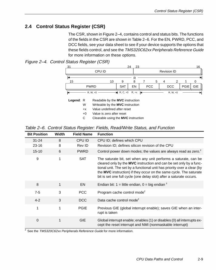
2-9CPU Data Paths and Control
2.4 Control Status Register (CSR)
The CSR, shown in Figure 2–4, contains control and status bits. The functionsof the fields in the CSR are shown in Table 2–6. For the EN, PWRD, PCC, andDCC fields, see your data sheet to see if your device supports the options thatthese fields control, and see the TMS320C62xx Peripherals Reference Guidefor more information on these options.
Figure 2–4. Control Status Register (CSR)31 24
CPU ID1623
Revision ID
R15
PWRD SAT EN PCC DCC
10 9 8 7 5 4 2 1 0
PGIE GIE
R, W, +0 R, +x R, W, +0R, C, +0
Legend : R Readable by the MVC instructionW Writeable by the MVC instruction+x Value undefined after reset+0 Value is zero after resetC Clearable using the MVC instruction
Table 2–6. Control Status Register: Fields, Read/Write Status, and FunctionBit Position Width Field Name Function
31-24 8 CPU ID CPU ID; defines which CPU23-16 8 Rev ID Revision ID; defines silicon revision of the CPU
15-10 6 PWRD Control power down modes; the values are always read as zero.†
9 1 SAT The saturate bit, set when any unit performs a saturate, can becleared only by the MVC instruction and can be set only by a func-tional unit. The set by a functional unit has priority over a clear (bythe MVC instruction) if they occur on the same cycle. The saturatebit is set one full cycle (one delay slot) after a saturate occurs.
8 1 EN Endian bit: 1 = little endian, 0 = big endian †
7-5 3 PCC Program cache control mode†
4-2 3 DCC Data cache control mode†
1 1 PGIE Previous GIE (global interrupt enable); saves GIE when an inter-rupt is taken
0 1 GIE Global interrupt enable; enables (1) or disables (0) all interrupts ex-cept the reset interrupt and NMI (nonmaskable interrupt)
† See the TMS320C62xx Peripherals Reference Guide for more information.

3-1 August 1996
Instruction Set
This chapter describes the assembly language instructions and addressingmodes for the ’C62xx digital signal processor. Also described are parallel op-erations, conditional operations, and resource constraints.
Topic Page
3.1 Instruction Operation and Execution Notations 3-2. . . . . . . . . . . . . . . . . .
3.2 Mapping Between Instructions and Functional Units 3-4. . . . . . . . . . . . .
3.3 TMS320C62xx Opcode Map 3-7. . . . . . . . . . . . . . . . . . . . . . . . . . . . . . . . . . .
3.4 Delay Slots 3-9. . . . . . . . . . . . . . . . . . . . . . . . . . . . . . . . . . . . . . . . . . . . . . . . . . .
3.5 Parallel Operations 3-10. . . . . . . . . . . . . . . . . . . . . . . . . . . . . . . . . . . . . . . . . . .
3.6 Conditional Operations 3-13. . . . . . . . . . . . . . . . . . . . . . . . . . . . . . . . . . . . . . .
3.7 Resource Constraints 3-14. . . . . . . . . . . . . . . . . . . . . . . . . . . . . . . . . . . . . . . .
3.8 Addressing Modes 3-18. . . . . . . . . . . . . . . . . . . . . . . . . . . . . . . . . . . . . . . . . . .
3.9 Individual Instruction Descriptions 3-21. . . . . . . . . . . . . . . . . . . . . . . . . . . .
Chapter 3

Instruction Operation and Execution Notations
3-2
3.1 Instruction Operation and Execution Notations
Table 3–1 explains the symbols used in this chapter.
Table 3–1. Instruction Operation and Execution Notations
Symbol Meaning
int 32-bit register value
long 40-bit register value
creg 3-bit field specifying a conditional register
cstn n-bit constant field
LSBn n least significant bits
MSBn n most significant bits
→ Assignment
+ Addition
– Subtraction
× Multiplication
+a Perform 2s-complement addition using the addressing mode defined bythe AMR
–a Perform 2s-complement subtraction using the addressing mode de-fined by the AMR
and Bitwise AND
or Bitwise OR
xor Bitwise exclusive OR
not Bitwise logical complement
by..z Selection of bits y through z of bit string b
<< Shift left
>>s Shift right with sign extension
>>z Shift right with a zero fill
x clear b,e Clear a field in x, specified by b (beginning bit) and e (ending bit)

Instruction Operation and Execution Notations
3-3Instruction Set
Table 3–1. Instruction Operation and Execution Notations (Continued)
Symbol Meaning
x exts l,r Extract and sign-extend a field in x, specified by l (shift left value) andr (shift right value)
x extu l,r Extract an unsigned field in x, specified by l (shift left value) and r (shiftright value)
+s Perform 2s-complement addition and saturate the result to the resultsize if an overflow occurs
–s Perform 2s-complement subtraction and saturate the result to the resultsize if an overflow occurs
x set b,e Set field in x to all 1s, specified by b (beginning bit) and e (ending bit)
abs(x) Absolute value of x
lmb0(x) Leftmost 0 bit search of x
lmb1(x) Leftmost 1 bit search of x
norm(x) Leftmost nonredundant sign bit of x
R Any general-purpose register
cond Check for either creg equal to zero or creg not equal to zero
nop No operation

Mapping Between Instructions and Functional Units
3-4
3.2 Mapping Between Instructions and Functional Units
Table 3–2 and Table 3–3 define the mapping between instructions and func-tional units.
Table 3–2. Instruction to Functional Unit Mapping
.L Unit .M Unit .S Unit .D Unit
ABS MPY ADD ADD
ADD SMPY ADDK ADDA
AND ADD2 LD mem
CMPEQ AND LD mem (15-bit offset)‡
CMPGT B disp MV
CMPGTU B IRP† NEG
CMPLT B NRP† ST mem
CMPLTU B reg ST mem (15-bit offset)‡
LMBD CLR SUB
MV EXT SUBA
NEG EXTU ZERO
NORM MVC†
NOT MV
OR MVK
SADD MVKH
SAT NEG
SSUB NOT
SUB OR
SUBC SET
XOR SHL
ZERO SHR
SHRU
SSHL
SUB
SUB2
XOR
ZERO
† .S2 only‡ .D2 only

Mapping Between Instructions and Functional Units
3-5Instruction Set
Table 3–3. Functional Unit to Instruction Mapping
’C62xx Functional Units
Instruction .L Unit .M Unit .S Unit .D Unit
ABS �
ADD � � �
ADDA �
ADDK �
ADD2 �
AND � �
B �
B IRP �†
B NRP �†
B reg �†
CLR �
CMPEQ �
CMPGT �
CMPGTU �
CMPLT �
CMPLTU �
EXT �
EXTU �
IDLE
LD mem �
LD mem(15-bit offset)
�‡
LMBD �
MPY �
MVC† �
MV � � �
MVK �
† .S2 only‡ .D2 only
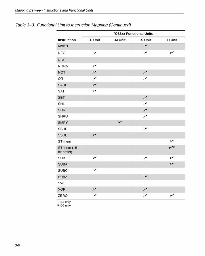
Mapping Between Instructions and Functional Units
3-6
Table 3–3. Functional Unit to Instruction Mapping (Continued)
’C62xx Functional Units
Instruction .L Unit .M Unit .S Unit .D Unit
MVKH �
NEG � � �
NOP
NORM �
NOT � �
OR � �
SADD �
SAT �
SET �
SHL �
SHR �
SHRU �
SMPY �
SSHL �
SSUB �
ST mem �
ST mem (15-bit offset)
�‡
SUB � � �
SUBA �
SUBC �
SUB2 �
SWI
XOR � �
ZERO � � �
† .S2 only‡ .D2 only

TMS320C62xx Opcode Map
3-7Instruction Set
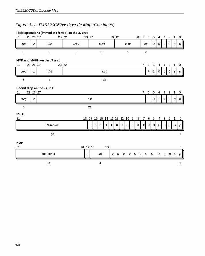
3.3 TMS320C62xx Opcode Map
The ’C62xx opcode map is shown in Figure 3–1. Refer to Table 3–1 and theinstruction descriptions in this chapter for explanations of the field syntaxesand values.
Figure 3–1. TMS320C62xx Opcode Map
31 29 28 27 23 22 18 17
creg z dst
13 12 11 5 4 3 2 1 0
x op 1 1 0 s p
Operations on the .L unit
3 5 5 5 7
src2 src1/cst
31 29 28 27 23 22 18 17
creg z dst src2
13 12 11 5 4 3 2 1 0
x op 0 0 0 s p
Operations on the .M unit
3 5 5 5 5
7 6
0 0src1/cst
31 29 28 27 23 22 18 17
creg z dst
13 12 5 4 3 2 1 0
op 0 0 0 s p
Operations on the .D unit
3 5 5 5 6
7 6
1 0src2 src1/cst
31 29 28 27 23 22
creg z dst/src
4 3 2 1 0
1 1 s p
Load/store with 15-bit offset (on the .D unit)
3 5 15
6
ld/stucst15
78
y
3
Load/store baseR + offsetR/cst on the .D unit31 29 28 27 23 22 18 17
creg z dst/src
13 12 9 8 7 6 4 3 2 1 0
mode r y ld/st 0 1 s p
3 5 5 5 4 3
baseR offsetR/ucst5
31 29 28 27 23 22 18 17
creg z dst
13 12 5 4 3 2 1 0
op 0 0 0 s p
Operations on the .S unit
3 5 5 5 6
6
1
11
xsrc1 /cstsrc 2
31 29 28 27 23 22
creg z dst
7 6 4 3 2 1 0
cst 0 0 s p
3 5 16
5
1 0 1
ADDK on the .S unit
TMS320C62xx Opcode Map
3-8
Figure 3–1. TMS320C62xx Opcode Map (Continued)
31 29 28 27 23 22 18 17
creg z dst
13 12 8 7 6 5 4 3 2 1 0
csta cstb op 0 0 1 0 s p
3 5 5 5 5 2
Field operations (immediate forms) on the .S unit
src2
31 29 28 27 23 22
creg z dst
7 6 5 4 3 2 1 0
1 0 1 0 s p
3 5 16
hdst
MVK and MVKH on the .S unit
Bcond disp on the .S unit31 29 28 27
creg z
7 6 5 4 3 2 1 0
0 1 0 0 s p
3 21
0cst
5 0
00 0 0 s p
31
Reserved
18 17 16
14
15
1
14 13 12 11 10 9 8 7 6
0 0 0 0 0 0 0 01 1 1 1
14 3 2IDLE
14
0
src 0 00 0 0 p
31
Reserved
18 17
1
16
4
13
0 0 0 0 0 0 0 0
NOP

Delay Slots
3-9Instruction Set
3.4 Delay Slots
The execution of instructions can be defined in terms of delay slots. The num-bered delay slots is equivalent to the number of extra cycles required beforea result is available for reading after the source operands are read. For asingle-cycle type instruction (such as ADD), source operands read in cycle iproduce a result that can be read in cycle i + 1. For a multiply instruction (MPY),source operands read in cycle i produce a result that can be read in cycle i + 2. Table 3–4 shows the number of delay slots associated with each typeof instruction.
Table 3–4. Delay Slot Summary
ÁÁÁÁÁÁÁÁÁÁÁÁÁÁÁÁÁÁÁÁÁÁÁÁÁÁÁÁÁÁÁÁÁÁ
Instruction Type ÁÁÁÁÁÁÁÁÁÁÁÁÁÁ
Delay SlotsÁÁÁÁÁÁÁÁÁÁÁÁÁÁÁÁÁÁÁÁÁÁÁÁÁÁÁÁÁÁÁÁÁÁ
NOP (no execution pipeline operation) ÁÁÁÁÁÁÁÁÁÁÁÁÁÁ
0ÁÁÁÁÁÁÁÁÁÁÁÁÁÁÁÁÁÁÁÁÁÁÁÁÁÁÁÁÁÁÁÁÁÁÁÁÁÁÁÁÁÁÁÁÁÁÁÁÁÁÁ
StoreÁÁÁÁÁÁÁÁÁÁÁÁÁÁÁÁÁÁÁÁÁ
0ÁÁÁÁÁÁÁÁÁÁÁÁÁÁÁÁÁÁÁÁÁÁÁÁÁÁÁÁÁÁÁÁÁÁÁÁÁÁÁÁÁÁÁÁÁÁÁÁÁÁÁ
Single cycle
ÁÁÁÁÁÁÁÁÁÁÁÁÁÁÁÁÁÁÁÁÁ
0
ÁÁÁÁÁÁÁÁÁÁÁÁÁÁÁÁÁÁÁÁÁÁÁÁÁÁÁÁÁÁÁÁÁÁ
Multiply ÁÁÁÁÁÁÁÁÁÁÁÁÁÁ
1
ÁÁÁÁÁÁÁÁÁÁÁÁÁÁÁÁÁÁÁÁÁÁÁÁÁÁÁÁÁÁÁÁÁÁ
Load (LD) (address modification occurs in E1)ÁÁÁÁÁÁÁÁÁÁÁÁÁÁ
4ÁÁÁÁÁÁÁÁÁÁÁÁÁÁÁÁÁÁÁÁÁÁÁÁÁÁÁÁÁÁÁÁÁÁ
Branch (The cycle when the target enters E1)ÁÁÁÁÁÁÁÁÁÁÁÁÁÁ
5
Parallel Operations
3-10
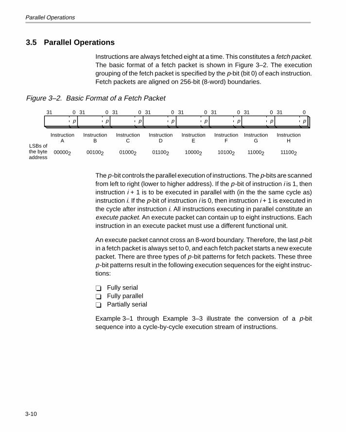
3.5 Parallel Operations
Instructions are always fetched eight at a time. This constitutes a fetch packet.The basic format of a fetch packet is shown in Figure 3–2. The executiongrouping of the fetch packet is specified by the p-bit (bit 0) of each instruction.Fetch packets are aligned on 256-bit (8-word) boundaries.
Figure 3–2. Basic Format of a Fetch Packet
p p p p p p p p
InstructionA
000002
InstructionB
001002
InstructionC
010002
InstructionD
011002
InstructionE
100002
InstructionF
101002
InstructionG
110002
InstructionH
111002
LSBs ofthe byteaddress
31 0 31 0 31 0 31 0 31 0 31 0 31 0 31 0
The p-bit controls the parallel execution of instructions. The p-bits are scannedfrom left to right (lower to higher address). If the p-bit of instruction i is 1, theninstruction i + 1 is to be executed in parallel with (in the the same cycle as)instruction i. If the p-bit of instruction i is 0, then instruction i + 1 is executed inthe cycle after instruction i. All instructions executing in parallel constitute anexecute packet. An execute packet can contain up to eight instructions. Eachinstruction in an execute packet must use a different functional unit.
An execute packet cannot cross an 8-word boundary. Therefore, the last p-bitin a fetch packet is always set to 0, and each fetch packet starts a new executepacket. There are three types of p-bit patterns for fetch packets. These threep-bit patterns result in the following execution sequences for the eight instruc-tions:
� Fully serial� Fully parallel� Partially serial
Example 3–1 through Example 3–3 illustrate the conversion of a p-bitsequence into a cycle-by-cycle execution stream of instructions.

Parallel Operations
3-11Instruction Set
Example 3–1. Fully Serial p-Bit Pattern in a Fetch Packet
This p-bit pattern:
0 0 0 0 0 0 0 0
InstructionA
InstructionB
InstructionC
InstructionD
InstructionE
InstructionF
InstructionG
InstructionH
31 0 31 0 31 0 31 0 31 0 31 0 31 0 31 0
results in this execution sequence:
Cycle/ExecutePacket Instructions
1 A
2 B
3 C
4 D
5 E
6 F
7 G
8 H
The eight instructions are executed sequentially.
Example 3–2. Fully Parallel p-Bit Pattern in a Fetch Packet
This p-bit pattern:
1 1 1 1 1 1 1 0
InstructionA
InstructionB
InstructionC
InstructionD
InstructionE
InstructionF
InstructionG
InstructionH
31 0 31 0 31 0 31 0 31 0 31 0 31 0 31 0
results in this execution sequence:
Cycle/ExecutePacket Instructions
1 A B C D E F G H
All eight instructions are executed in parallel.

Parallel Operations
3-12
Example 3–3. Partially Serial p-Bit Pattern in a Fetch Packet
This p-bit pattern:
31 0 31 0 31 0 31 0
0 0 1 1
31 0 31 0 31 0 31 0
0 1 1 0
InstructionA
InstructionB
InstructionC
InstructionD
InstructionE
InstructionF
InstructionG
InstructionH
results in this execution sequence:
Cycle/Execute Packet Instructions
1 A
2 B
3 C D E
4 F G H
Note: Instructions C, D, and E do not use any of the same functional units, cross paths, or otherdata path resources. This is also true for instructions F, G, and H.
3.5.1 Example Parallel Code
The || characters signify that an instruction is to execute in parallel with the pre-vious instruction. The code for the fetch packet in Example 3–3 would be rep-resented as this:
instruction A
instruction B
instruction C|| instruction D|| instruction E
instruction F|| instruction G|| instruction H
3.5.2 Branching Into the Middle of an Execute Packet
If a branch into the middle of an execution packet occurs, all instructions at low-er addresses are ignored. In Example 3–3, if a branch to the address contain-ing instruction D occurs, then only D and E execute. Even though instructionC is in the same execute packet, it is ignored. Instructions A and B are alsoignored because they are in earlier execute packets.

Conditional Operations
3-13Instruction Set
3.6 Conditional Operations
All instructions can be conditional. The condition is controlled by a 3-bit opcodefield (creg) that specifies the condition register tested, and a 1-bit field (z) thatspecifies a test for zero or nonzero. The four MSBs of every opcode are cregand z. The register is tested at the beginning of the E1 pipeline stage for allinstructions. For more information on the pipeline, see Chapter 4, Pipeline Op-eration. If z = 1, the test is for equality with zero. If z = 0, the test is for nonzero.The case of creg = 0 and z = 0 is treated as always true to allow instructionsto be executed unconditionally. The creg field is encoded in the instruction op-code as shown in Table 3–5.
Table 3–5. Registers That Can Be Tested by Conditional Operations
Conditionalcreg z
ConditionalRegister Bit 31 30 29 28
Unconditional 0 0 0 0
Reserved 0 0 0 1
B0 0 0 1 z
B1 0 1 0 z
B2 0 1 1 z
A1 1 0 0 z
A2 1 0 1 z
Reserved 1 1 x x
Note: x can be any value in reserved cases.
Conditional instructions are represented by using square brackets, [ ], sur-rounding the condition register. The following execute packet contains twoADD instructions in parallel. The first ADD is conditional on B0 being nonzero.The second ADD is conditional on B0 being zero. The character ! indicates the‘not’ of the condition.
[B0] ADD .L1 A1,A2,A3|| [!B0] ADD .L2 B1,B2,B3
The above instructions are mutually exclusive. This means that only one willexecute.
If they are scheduled in parallel, mutually exclusive instructions areconstrained as described in section 3.7. If mutually exclusive instructionsshare any resources as described in section 3.7, they cannot be scheduled inparallel (put in the same execute packet), even though only one will execute.

Resource Constraints
3-14
3.7 Resource Constraints
No two instructions within the same execute packet can use the same re-sources. Also, no two instructions can write to the same register during thesame cycle. The following sections, 3.7.1 to 3.7.5, describe each of the re-sources an instruction can use.
3.7.1 Constraints on Instructions Using the Same Functional Unit
Two instructions using the same functional unit cannot be issued in the sameexecute packet.
The following execute packet is invalid:
ADD .S1 A0, A1, A2 ; \ .S1 is used for|| SHR .S1 A3, 15, A4 ; / both instructions
The following execute packet is valid:
ADD .L1 A0, A1, A2 ; \ Two different functional|| SHR .S1 A3, 15, A4 ; / units are used
3.7.2 Constraints on Cross Paths (1X and 2X)
One unit (either a .S, .L, or .M unit) per data path, per execute packet, can reada source operand from its opposite register file via the cross paths (1X and 2X).For example, .S1 can read both of an instruction’s operands from the A registerfile, or it can read one operand from the B register file using the 1X cross pathand the other from the A register file. This is denoted by an X following the unitname in the instruction syntax.
Two instructions using the same cross path between register files cannot beissued in the same execute packet, because there is only one path from A toB and one path from B to A.
The following execute packet is invalid:
ADD.L1X A0,B1,A1 ; \ 1X cross path is used|| MPY.M1X A4,B4,A5 ; / for both instructions
The following execute packet is valid:
ADD.L1X A0,B1,A1 ; \ Instructions use the 1X and|| MPY.M2X B4,A4,B2 ; / 2X cross paths
The operand will come from a register file opposite of the destination if the xbit in the instruction field is set (shown in the opcode map located in sec-tion 3.3).

Resource Constraints
3-15Instruction Set
3.7.3 Constraints on Loads and Stores
Loads and stores can use an address pointer from one register file while load-ing to or storing from the other register file. Two loads and/or stores using anaddress pointer from the same register file cannot be issued in the sameexecute packet.
The following execute packet is invalid:
LDW.D1 *A0,A1 ; \ Address registers from the same|| LDW.D1 *A2,B2 ; / register file
The following execute packet is valid:
LDW.D1 *A0,A1 ; \ Address registers from different|| LDW.D2 *B0,B2 ; / register files
Two loads and/or stores loading to and/or storing from the same register filecannot be issued in the same execute packet.
The following execute packet is invalid:
LDW.D1 *A4,A5 ; \ Loading to and storing from the|| STW.D2 A6,*B4 ; / same register file
The following execute packet is valid:
LDW.D1 *A4,B5 ; \ Loading to, and storing from|| STW.D2 A6,*B4 ; / different register files
3.7.4 Constraints on Long (40-Bit) Data
Because the .S and .L units share a read register port for long source operandsand a write register port for long results, only one long result may be issuedper register file in an execute packet. See section 2.1.1, on page 2-2 for theorder for long pairs.
The following execute packet is invalid:
ADD.L1 A5:A4,A1,A3:A2 ; \ Two long writes|| SHL.S1 A8,A9,A7:A6 ; / on A register file
The following execute packet is valid:
ADD.L1 A5:A4,A1,A3:A2 ; \ One long write for|| SHL.S2 B8,B9,B7:B6 ; / each register file
Because the .L and .S units share their long read port with the store port, op-erations that read a long value cannot be issued on the .L and/or .S units inthe same execute packet as a store.

Resource Constraints
3-16
The following execute packet is invalid:
ADD .L1 A5:A4,A1,A3:A2 ; \ Long read operation and a|| STW .D1 A8,*A9 ; / store
The following execute packet is valid:
ADD.L1 A4, A1, A3:A2 ; \ No long read with|| STW.D1 A8,*A9 ; / with the store
3.7.5 Constraints on Register Reads
More than four reads of the same register cannot occur on the same cycle.Conditional registers are not included in this count.
The following code sequence is invalid:
MPY .M1 A1,A1,A4 ; five reads of register A1|| ADD .L1 A1,A1,A5|| SUB .D1 A1,A2,A3
This code sequence is valid:
MPY .M1 A1,A1,A4 ; only four reads of A1|| [A1] ADD .L1 A0,A1,A5|| SUB .D1 A1,A2,A3
3.7.6 Constraints on Register Writes
Multiple writes to the same register on the same cycle can occur if instructionswith different latencies writing to the same register are issued on differentcycles. For example, an MPY issued on cycle i followed by an ADD on cyclei + 1 cannot write to the same register because both instructions write a resulton cycle i + 1. Therefore, the following code sequence is invalid:
MPY .M1 A0,A1,A2 ADD .L1 A4,A5,A2

Resource Constraints
3-17Instruction Set
Figure 3–3 shows different multiple-write conflicts. For example, ADD andSUB in execute packet L1 write to the same register. This conflict is easily de-tectable.
MPY in packet L2 and ADD in packet L3 might both write to B2 simultaneously;however, if a branch instruction causes the execute packet after L2 to besomething other than L3, a conflict would not occur. Thus, the potential conflictin L2 and L3 might not be detected by the assembler. The instructions in L4do not constitute a write conflict because they are mutually exclusive. In con-trast, because it is not obvious that the instructions in L5 are mutually exclu-sive, the assembler cannot determine a conflict. If the pipeline does receivecommands to perform multiple writes to the same register, the result is unde-fined.
Figure 3–3. Examples of the Detectability of Write Conflicts by the Assembler
L1: ADD.L2 B5,B6,B7 ; \ detectable, conflict|| SUB.S2 B8,B9,B7 ; /
L2: MPY.M2 B0,B1,B2 ; \ not detectable
L3: ADD.L2 B3,B4,B2 ; /
L4:[!B0] ADD.L2 B5,B6,B7 ; \ detectable, no conflict|| [B0] SUB.S2 B8,B9,B7 ; /
L5:[!B1] ADD.L2 B5,B6,B7 ; \ not detectable|| [B0] SUB.S2 B8,B9,B7 ; /

Addressing Modes
3-18
3.8 Addressing Modes
The addressing modes on the ’C62xx are linear, circular using BK0, and circu-lar using BK1. The mode is specified by the addressing mode register, or AMR(defined in Chapter 2).
Eight registers can perform circular addressing. A4-A7 are used by the .D1 unitand B4-B7 are used by the .D2 unit. No other units can perform circular addres-sing. All registers can perform linear addressing. LD(B)(H)(W) , ST(B)(H)(W),ADDA(B)(H)(W) , and SUBA(B)(H)(W) instructions all use the AMR to deter-mine what type of address calculations are performed for these registers.
3.8.1 Linear Addressing Mode
LD/ST instructions
Linear mode simply shifts the offsetR/cst operand to the left by 2, 1, or 0 forword, half-word, or byte access, respectively, and then performs an add or asubtract to baseR (depending on the operation specified).
ADDA/SUBA instructions
Linear mode simply shifts the src1/cst operand to the left by 2, 1, or 0 for word,halfword, or byte data sizes, respectively, and then performs the add or sub-tract specified.
3.8.2 Circular Addressing Mode
The BK0 and BK1 fields in the AMR specify block sizes for circular addressing.See section 2.3 for more information on the AMR.
LD/ST Instructions
After shifting offsetR/cst to the left by 2, 1, or 0 for LDW, LDH, or LDB , respec-tively, an add or subtract is performed with the carry/borrow inhibited betweenbits N and N + 1. Bits N + 1 to 31 of baseR remain unchanged. All other carries/borrows propagate as usual. If you specify an offsetR/cst greater than the cir-cular buffer size, 2(N + 1), the effective offsetR/cst is modulo the circular buffersize (see Example 3–4). The circular buffer size in the AMR is not scaled; forexample: a block size of 4 is 4 bytes, not 4 × data size (byte, halfword, word).So, to perform circular addressing on an array of 8 words, a size of 32 shouldbe specified, or N = 4. Example 3–4 shows a LDW performed with register A4in circular mode and BK0 = 4, so the buffer size is 32 bytes, 16 halfwords, or8 words. The value put in the AMR for this example is 0004 0001h.

Addressing Modes
3-19Instruction Set
Example 3–4. LDW in Circular Mode
LDW .D1 *++A4[9],A1
Before LDW 1 cycle after LDW 5 cycles after LDW
A4 0000 0100h A4 0000 0104h A4 XXXX XXXXh
A1 XXXX XXXXh A1 XXXX XXXXh A1 0000 0100h
mem 104h 1234 5678h mem 104h XXXX XXXXh mem 104h XXXX XXXXh
Note: 9h words is 24h bytes. 24h bytes is 4 bytes beyond the 32-byte (20h) boundary 100h–11Fh; thus, it is wrapped around to104h.
ADDA/SUBA Instructions
After shifting src1/cst to the left by 2, 1, or 0 for ADDAW, ADDAH , or ADDAB ,respectively, an add or a subtract is performed with the carry/borrow inhibitedbetween bits N and N + 1. Bits N + 1 to 31 (inclusive) of src2 remain unchanged.All other carries/borrows propagate as usual. If you specify src1 greater thanthe circular buffer size, 2(N + 1), the effective offsetR/cst is modulo the circularbuffer size (see Example 3–5). The circular buffer size in the AMR is notscaled; for example, a block size of 4 is 4 bytes, not 4 × data size (byte, half-word, word). So, to perform circular addressing on an array of 8 words, a sizeof 32 should be specified, or N = 4. Example 3–5 shows an ADDAH performedwith register A4 in circular mode and BK0 = 4, so the buffer size is 32 bytes,16 halfwords, or 8 words. The value put in the AMR for this example is0004 0001h.
Example 3–5. ADDAH in Circular Mode
ADDAH .D1 A4,A1,A1
Before ADDAH1 cycle after ADDAH
A4 0000 0100h A4 0000 0106h
A1 0000 0013h A1 XXXX XXXXh
Note: 13h halfwords is 26h bytes. 26h bytes is 6 bytes beyond the 32-byte (20h) boundary100h–11Fh; thus, it is wrapped around to 106h.

Addressing Modes
3-20
3.8.3 Syntax for Load/Store Address Generation
The ’C62xx CPU has a load/store architecture, which means that the only wayto access data in memory is with a load or store instruction. Table 3–6 showsthe syntax of an indirect address to a memory location.
Table 3–6. Indirect Address Generation for Load/Store
Addressing TypeNo Modification of Address Register
Preincrement orDecrement of
Address Register
Postincrement Decrement of Address
Register
Register indirect *R*++R*– –R
*R++*R– –
Register relative*+R[ucst5]*–R[ucst5]
*++R[ucst5]*– –R[ucst5]
*R++[ucst5]*R– –[ucst5]
Base + index*+R[offsetR]*–R[offsetR]
*++R[offsetR]*– –R[offsetR]
*R++[offsetR]*R– –[offsetR]

Individual Instruction Descriptions
3-21Instruction Set
3.9 Individual Instruction Descriptions
This section gives detailed information on the instruction set for the ’C62xx.Each instruction presents the following information:
� Assembler syntax� Functional units� Operands� Opcode� Description� Execution� Instruction type� Delay slots� Examples
An example instruction description is provided before the actual instruction de-scriptions (starting with the ABS instruction description). The example is pro-vided to familiarize you with how the instructions are described. It includes anddescribes information pulled from the ADD instruction description, giving basicinformation about what each description category provides and where to gofor more information.

Individual Instruction Descriptions
3-22
Syntax EXAMPLE (.unit) src, dst.unit = .L1, .L2, .S1, .S2, .D1, .D2
src and dst indicate source and destination, respectively. The (.unit) dictateswhich functional unit the instruction is mapped to (.L1, .L2, .S1, .S2, .M1, .M2,.D1, or .D2).
A table is provided for each instruction that gives the opcode map fields, unitsthe instruction is mapped to, types of operands, and the opcode.
The opcode map breaks down the various bit fields that make up each instruc-tion. These fields are illustrated in section 3.3.
There are instructions that can be executed on more than one functional unit.Table 3–7 shows how this situation is documented for the ADD instruction.This instruction has three opcode map fields: src1, src2, and dst. In theseventh row, the operands have the types cst5, long, and long for src1, src2,and dst, respectively. The ordering of these fields implies cst5 + long � long,where + represents the operation being performed by the ADD. This operationcan be done on .L1 or .L2 (both are specified in the unit column). The s in frontof each operand signifies that src1 (scst5), src2 (slong), and dst (slong) are allsigned values.
In the third row, src1, src2, and dst are int, int, and long, respectively. The u infront of each operand signifies that all operands are unsigned. Any operandthat begins with x can be read from a register file that is different from the des-tination register file. The operand comes from the register file opposite the des-tination if the x bit in the instruction field is set (shown in the opcode map lo-cated in section 3.3).
EXAMPLE Example Instruction

Example Instruction EXAMPLE
3-23 Instruction Set
Table 3–7. Relationships Between Operands, Operand Size, Signed/Unsigned, FunctionalUnits, and Opfields for Example Instruction (ADD Instruction)
Opcode map field used... For operand type... Unit Opfield Mnemonic
src1src2dst
sintxsintsint
.L1, .L2 0000011 ADD
src1src2dst
sintxsintslong
.L1, .L2 0100011 ADD
src1src2dst
uintxunitulong
.L1, .L2 0101011 ADDU
src1src2dst
xsintslongslong
.L1, .L2 0100001 ADD
src1src2dst
xuintulongulong
.L1, .L2 0101001 ADDU
src1src2dst
scst5xsintsint
.L1, .L2 0000010 ADD
src1src2dst
scst5slongslong
.L1, .L2 0100000 ADD
src1src2dst
sintxsintsint
.S1, .S2 000111 ADD
src1src2dst
scst5xsintsint
.S1, .S2 000110 ADD
src2src1dst
sintsintsint
.D1, .D2 010000 ADD
src2src1dst
sintucst5sint
.D1, .D2 010010 ADD

EXAMPLE Example Instruction
3-24
Description Instruction execution and its effect on the rest of the processor or memory con-tents are described. Any constraints on the operands imposed by the proces-sor or the assembler are discussed. The description parallels and supple-ments the information given by the execution block.
Execution for .L1, .L2 and .S1, .S2 opcodesif (cond) src1 + src2 → dstelse nop
Execution for .D1, .D2 opcodesif (cond) src2 + src1 → dstelse nop
The execution describes the processing that takes place when the instructionis executed. The symbols are defined in Table 3–1 on page 3-2.
Instruction Type This section gives the type of instruction. See section 4.2.
Delay Slots This section gives the number of delay slots the instruction takes to execute(see section 3.4).
Example Examples of instruction execution. If applicable, register and memory valuesare given before and after instruction execution.

Integer Absolute Value With Saturation ABS
3-25 Instruction Set
Syntax ABS (.unit) src2, dst
.unit = .L1, .L2
Opcode map field used... For operand type... Unit Opfield
src2dst
xsintsint
.L1, .L2 0011010
src2dst
slongslong
.L1, L2 0111000
Description The absolute value of src2 is placed in dst.
Execution if (cond) abs(src2) → dstelse nop
The absolute value of src2 when src2 is an int is determined as follows:
1) If src2 � 0, then src2 → dst2) If src2 � 0 and src2 � –231, then –src2 → dst3) If src2 = –231, then 231–1 → dst
The absolute value of src2 when src2 is a long is determined as follows:
1) If src2 � 0, then src2 → dst2) If src2 � 0 and src2 � –239, then –src2 → dst3) If src2 = –239, then 239 – 1 → dst
Instruction Type Single-cycle
Delay Slots 0
Example 1 ABS .L1 A1,A5
Before instruction 1 cycle after instruction
A1 8000 4E3Dh –2147463619 A1 8000 4E3Dh –2147463619
A5 XXXX XXXXh A5 7FFF B1C3h 2147463619
Example 2 ABS .L1 A1,A5
Before instruction 1 cycle after instruction
A1 3FF6 0010h 1073086480 A1 3FF6 0010h 1073086480
A5 XXXX XXXXh A5 3FF6 0010h 1073086480

ADD(U) Integer Addition Without Saturation (Signed or Unsigned)
3-26
Syntax ADD (.unit) src1, src2, dstor
ADDU (.unit) src1, src2, dstor
ADD (.unit) src2, src1, dst
.unit = .L1, .L2, .S1, .S2, .D1, .D2
Opcode map field used... For operand type... Unit Opfield
src1src2dst
sintxsintsint
.L1, .L2 0000011
src1src2dst
sintxsintslong
.L1, .L2 0100011
src1src2dst
uintxunitulong
.L1, .L2 0101011
src1src2dst
xsintslongslong
.L1, .L2 0100001
src1src2dst
xuintulongulong
.L1, .L2 0101001
src1src2dst
scst5xsintsint
.L1, .L2 0000010
src1src2dst
scst5slongslong
.L1, .L2 0100000
src1src2dst
sintxsintsint
.S1, .S2 000111
src1src2dst
scst5xsintsint
.S1, .S2 000110
src2src1dst
sintsintsint
.D1, .D2 010000
src2src1dst
sintucst5sint
.D1, .D2 010010

Integer Addition Without Saturation (Signed or Unsigned) ADD(U)
3-27 Instruction Set
Description for .L1, .L2 and .S1, .S2 opcodessrc2 is added to src1. The result is placed in dst.
Execution for .L1, .L2 and .S1, .S2 opcodesif (cond) src1 + src2 → dstelse nop
Description for .D1, .D2 opcodessrc1 is added to src2. The result is placed in dst.
Execution for .D1, .D2 opcodesif (cond) src2 + src1 → dstelse nop
Instruction Type Single-cycle
Delay Slots 0
Example 1 ADD .L2 A1,B1,B2
Before instruction 1 cycle after instruction
A1 0000 325Ah 12890 A1 0000 325Ah
B1 FFFF FF12h –238 B1 FFFF FF12h
B2 XXXX XXXXh B2 0000 316Ch 12652
Example 2 ADDU .L1 A1,A2,A5:A4
Before instruction 1 cycle after instruction
A1 0000 325Ah †12890 A1 0000 325Ah
A2 FFFF FF12h †4294967058 A2 FFFF FF12h
A5:A4 XXXX XXXX A5:A4 0000 0001h 0000 316Ch ‡4294979948
Example 3 ADDU .L1 A1,A3:A2,A5:A4
Before instruction 1 cycle after instruction
A1 0000 325Ah 12890 A1 0000 325Ah
A3:A2 0000 00FFh FFFF FF12h ‡1099511627538 A3:A2 0000 00FFh FFFF FF12h
A5:A4 0000 0000h 0000 0000h 0 A5:A4 0000 0000h 0000 316Ch ‡12652
† Unsigned 32-bit integer‡ Unsigned 40-bit (long) integer

ADD(U) Integer Addition Without Saturation (Signed or Unsigned)
3-28
Example 4 ADD .L1 A1,A3:A2,A5:A4
Before instruction 1 cycle after instruction
A1 0000 325Ah 12890 A1 0000 325Ah
A3:A2 0000 00FFh FFFF FF12h §–228 A3:A2 0000 00FFh FFFF FF12h
A5:A4 0000 0000h 0000 0000h §0 A5:A4 0000 0000h 0000 316Ch §12652
§ Signed 40-bit (long) integer
Example 5 ADD .L1 –13,A1,A6
Before instruction 1 cycle after instruction
A1 0000 325Ah 12890 A1 0000 325Ah
A6 XXXX XXXXh A6 0000 324Dh 12877
Example 6 ADD .D1 26,A1,A6
Before instruction 1 cycle after instruction
A1 0000 325Ah 12890 A1 0000 325Ah
A6 XXXX XXXXh A6 0000 3274h 12916

Integer Addition Using Addressing Mode ADDA(B)(H)(W)
3-29 Instruction Set
Syntax ADDAB (.unit) src2, src1, dstor
ADDAH (.unit) src2, src1, dstor
ADDAW (.unit) src2, src1, dst
.unit = .D1 or .D2
Opcode map field used... For operand type... Unit Opfield
src2src1dst
sintsintsint
.D1, .D2 byte: 110000halfword: 110100
word: 111000
src2src1dst
sintucst5sint
.D1, .D2 byte: 110010halfword: 110110
word: 111010
Description src1 is added to src2 using the addressing mode specified for src2. The addi-tion defaults to linear mode. However, if src2 is one of A4–A7 or B4–B7, themode can be changed to circular mode by writing the appropriate value to theAMR (see section 2.3). src1 is left shifted by 1 or 2 for halfword and word datasizes respectively. Byte, halfword, and word mnemonics are ADDAB , ADD-AH, and ADDAW, respectively. The result is placed in dst.
Execution if (cond) src2 +a src1 → dstelse nop
Instruction Type Single-cycle
Delay Slots 0
Example 1 ADDAB .D1 A4,A2,A4
Before instruction 1 cycle after instruction
A2 0000 000Bh A2 0000 000Bh
A4 0000 0100h A4 0000 0103h
AMR 0002 0001h AMR 0002 0001h
BK0 = 2 → size = 8A4 in circular addressing mode using BK0

ADDA(B)(H)(W) Integer Addition Using Addressing Mode
3-30
Example 2 ADDAH .D1 A4,A2,A4
Before instruction 1 cycle after instruction
A2 0000 000Bh A2 0000 000Bh
A4 0000 0100h A4 0000 0106h
AMR 0000 0000h AMR 0000 0000h
BK0 = 2 → size = 8A4 in linear addressing mode
Example 3 ADDAW .D1 A4,2,A4
Before instruction 1 cycle after instruction
A4 0002 0000h A4 0002 0000h
AMR 0002 0001h AMR 0002 0001h
BK0 = 2 → size = 8A4 in circular addressing mode using BK0

Integer Addition Using Signed 16-Bit Constant ADDK
3-31 Instruction Set
Syntax ADDK (.unit) cst, dst
.unit = .S1 or .S2
Opcode
165
z dst
6 0
cst 1 0 1 0 0 s p
31
creg
29 28 27 23 22 7
13 1 1
Opcode map field used... For operand type... Unit
cstdst
scst16uint
.S1, .S2
Description A 16-bit signed constant is added to the dst register specified. The result isplaced in dst.
Execution if (cond) cst + dst → dstelse nop
Instruction Type Single-cycle
Delay Slots 0
Example ADDK .S1 15401,A1
Before instruction 1 cycle after instruction
A1 0021 37E1h 2176993 A4 0021 740Ah 2192394

ADD2 Two 16-Bit Integer Adds on Upper and Lower Register Halves
3-32
Syntax ADD2 (.unit) src1, src2, dst
.unit = .S1 or .S2
Opcode map field used... For operand type... Unit Opfield
src1src2dst
sintxsintsint
.S1, .S2 000001
Description The upper and lower halves of the src1 operand are added to the upper andlower halves of the src2 operand. Any carry from the lower half add does notaffect the upper half add.
Execution if (cond) {((lsb16(src1) + lsb16(src2)) and FFFFh) or
((msb16(src1) + msb16(src2)) << 16) → dst}
else nop
Instruction Type Single-cycle
Delay Slots 0
Example ADD2 .S1 A1,B1,A2
Before instruction 1 cycle after instruction
A1 0021 37E1h 2176993 A1 0021 37E1h
A2 XXXX XXXXh A2 03BC 1C99h 62659737
B1 039A E4B8h 60482744 B1 039A E4B8h

Bitwise AND AND
3-33 Instruction Set
Syntax AND (.unit) src1, src2, dst
.unit = .L1 or .L2, .S1 or .S2
Opcode map field used... For operand type... Unit Opfield
src1src2dst
uintxuintuint
.L1, .L2 1111001
src1src2dst
scst5xuintuint
.L1, .L2 1111010
src1src2dst
uintxuintuint
.S1, .S2 011111
src1src2dst
scst5xuintuint
.S1, .S2 011110
Description A bitwise AND is performed between src1 and src2. The result is placed in dst.The scst5 operands are sign extended to 32 bits.
Execution if (cond) src1 and src2 → dstelse nop
Delay Slots 0
Example 1 AND .L1 A1,B1,A2
Before instruction 1 cycle after instruction
A1 F7A1 302Ah A1 F7A1 302Ah
A2 XXXX XXXXh A2 02A0 2020h
B1 02B6 E724h B1 02B6 E724h
Example 2 AND .L1 15,A1,A3
Before instruction 1 cycle after instruction
A1 32E4 6936h A1 32E4 6936h
A3 XXXX XXXXh A3 0000 0006h

B Branch Using a Displacement
3-34
Syntax B (.unit) label
.unit = .S1 or .S2
Opcode
21
z
6 0
cst 1 0 1 0 0 s p
31
creg
29 28 27 7
13 1 1
Opcode map field used... For operand type... Unit
cst scst21 .S1, .S2
Description A 21-bit signed constant specified by cst is shifted left by 2 bits and is addedto the address of the first instruction of the fetch packet that contains thebranch instruction. The result is placed in the program fetch counter (PFC).The assembler/linker automatically computes the correct value for cst by thefollowing formula:
cst = (label – PCE1) >> 2
If two branches are in the same execute packet and both are taken, behavioris undefined.
Two conditional branches can be in the same execute packet only if one ofthem is B using a register, B IRP, or B NRP. As long as only one branch hasa true condition, code executes in a normal, well-defined way.
Execution if (cond) cst << 2 + PCE1 → PFCelse nop
Notes:
1) PCE1 (program counter) represents the address of the first instructionin the fetch packet in the E1 stage of the pipeline. PFC is the programfetch counter.
2) An execute packet containing a branch and the execute packets in itsdelay slots cannot be interrupted. This is true regardless of whether thebranch is taken.
3) See section 3.5.2 on page 3-12 for information on branching into themiddle of an execute packet.
Instruction Type Branch
Delay Slots 5

Branch Using a Displacement B
3-35 Instruction Set
Table 3–8 gives the program counter values and actions for the following codeexample.
Example
0000 0000 B .S1 LOOP0000 0004 ADD .L1 A1, A2, A30000 0008 || ADD .L2 B1, B2, B30000 000C LOOP: MPY .MIX A3, B3, A40000 0010 || SUB .D1 A5, A6, A60000 0014 MPY .M1 A3, A6, A50000 0018 MPY .M2 A6, A7, A80000 001C SHR .S1 A4, 15, A40000 0020 ADD .D1 A4, A6, A4
Table 3–8. Program Counter Values for Branch Using a Displacement Example
Cycle Program Counter Value Action
Cycle 0 0000 0000h Branch command executes(target code fetched)
Cycle 1 0000 0004h
Cycle 2 0000 000Ch
Cycle 3 0000 0014h
Cycle 4 0000 0018h
Cycle 5 0000 001Ch
Cycle 6 0000 000Ch Branch target codeexecutes
Cycle 7 0000 0014h

B Branch Using a Register
3-36
Syntax B (.unit) src2
.unit = .S2
Opcode map field used... For operand type... Unit Opfield
src2 xuint .S2 001101
Description src2 is placed in the PFC.
If two branches are in the same execute packet and are both taken, behavioris undefined.
Two conditional branches can be in the same execute packet only if one ofthem is B using a register, B IRP, or B NRP. As long as only one branch hasa true condition, code executes in a normal, well-defined way.
Execution if (cond) src2 → PFCelse nop
Notes:
1) This instruction executes on .S2 only. PFC is program fetch counter.
2) An execute packet containing a branch and the execute packets in itsdelay slots cannot be interrupted. This is true regardless of whether thebranch is taken.
Instruction Type Branch
Delay Slots 5

Branch Using a Register B
3-37 Instruction Set
Table 3–9 gives the program counter values and actions for the following codeexample. In this example, the B10 register holds the value 0000 0003.
Example B10 0000 0003
0000 0000 B .S2 B100000 0004 ADD .L1 A1, A2, A30000 0008 || ADD .L2 B1, B2, B30000 000C MPY .MIX A3, B3, A40000 0010 || SUB .D1 A5, A6, A60000 0014 MPY .M1 A3, A6, A50000 0018 MPY .M2 A6, A7, A80000 001C SHR .S1 A4, 15, A40000 0020 ADD .D1 A4, A6, A4
Table 3–9. Program Counter Values for Branch Using a Register Example
Cycle Program Counter Value Action
Cycle 0 0000 0000h Branch command executes(target code fetched)
Cycle 1 0000 0004h
Cycle 2 0000 000Ch
Cycle 3 0000 0014h
Cycle 4 0000 0018h
Cycle 5 0000 001Ch
Cycle 6 0000 000Ch Branch target codeexecutes
Cycle 7 0000 0014h

B IRP Branch Using an Interrupt Return Pointer
3-38
Syntax B (.unit) IRP
.unit = .S2
Opcode map field used... For operand type... Unit Opfield
src2 xsint .S2 000011
Description IRP is placed in the PFC. This instruction also moves PGIE to GIE. PGIE isunchanged.
If two branches are in the same execute packet and are both taken, behavioris undefined.
Two conditional branches can be in the same execute packet only if one ofthem is B using a register, B IRP, or B NRP. As long as only one branch hasa true condition, code executes in a normal, well-defined way.
Execution if (cond) IRP → PFCelse nop
Notes:
1) This instruction executes on .S2 only. PFC is the program fetch counter.
2) Refer to the chapter on interrupts for more information on IRP, PGIE, andGIE.
3) An execute packet containing a branch and the execute packets in itsdelay slots cannot be interrupted. This is true regardless of whether thebranch is taken.
Instruction Type Branch
Delay Slots 5

Branch Using an Interrupt Return Pointer B IRP
3-39 Instruction Set
Table 3–10 gives the program counter values and actions for the followingcode example.
Example Given that an interrupt occurred at PC = 0000 0100 IRP = 0000 0100→ :
0000 0000 B .S2 IRP0000 0004 ADD .S1 A0, A2, A10000 0008 MPY .M1 A1, A0, A10000 000C NOP0000 0010 SHR .S1 A1, 15, A10000 0014 ADD .L1 A1, A2, A10000 0018 ADD .L2 B1, B2, B3
Table 3–10. Program Counter Values for B IRP Example
Cycle Program Counter Value Action
Cycle 0 0000 0000 Branch command executes(target code fetched)
Cycle 1 0000 0004
Cycle 2 0000 0008
Cycle 3 0000 000C
Cycle 4 0000 0010
Cycle 5 0000 0014
Cycle 6 0000 0100 Branch target code executes

B NRP Branch Using NMI Return Pointer
3-40
Syntax B (.unit) NRP
.unit = .S2
Opcode map field used... For operand type... Unit Opfield
src2 xsint .S2 000011
Description NRP is placed in the PFC. This instruction also sets NMIE. PGIE is unchanged.
If two branches are in the same execute packet and are both taken, behavioris undefined.
Two conditional branches can be in the same execute packet only if one ofthem is B using a register, B IRP, or B NRP. As long as only one branch hasa true condition, code executes in a normal, well-defined way.
Execution if (cond) NRP → PFCelse nop
Notes:
1) This instruction executes on .S2 only. PFC is program fetch counter.
2) Refer to the chapter on interrupts for more information on NRP andNMIE.
3) An execute packet containing a branch and the execute packets in itsdelay slots cannot be interrupted. This is true regardless of whether thebranch is taken.
Instruction Type Branch
Delay Slots 5

Branch Using NMI Return Pointer B NRP
3-41 Instruction Set
Table 3–11 gives the program counter values and actions for the followingcode example.
Example Given that an interrupt occurred at PC = 0000 0100 NRP = 0000 0100→ :
0000 0000 B .S2 NRP0000 0004 ADD .S1 A0, A2, A10000 0008 MPY .M1 A1, A0, A10000 000C NOP0000 0010 SHR .S1 A1, 15, A10000 0014 ADD .L1 A1, A2, A10000 0018 ADD .L2 B1, B2, B3
Table 3–11. Program Counter Values for B NRP Example
Cycle Program Counter Value Action
Cycle 0 0000 0000 Branch command executes(target code fetched)
Cycle 1 0000 0004
Cycle 2 0000 0008
Cycle 3 0000 000C
Cycle 4 0000 0010
Cycle 5 0000 0014
Cycle 6 0000 0100 Branch target code executes
CLR Clear a Bit Field
3-42
Syntax CLR (.unit) src2, csta, cstb, dstor
CLR (.unit) src2, src1, dst
.unit = .S1 or .S2
Opcode
Constant form:
5
z cstb
6 5 0
dst 0 0 1 0 s p
31
creg
29 28 27 7
13
18 1723 22
src2
5
csta
13
5
12 8
5 2 1 1
1 0
Register form:
5
z
6 5 0
dst 1 0 0 0 s p
31
creg
29 28 27
13
18 1723 22
src2
5
src1
13
5
12
6 1 1
x
1
11
1 1 1 0 1 1
Opcode map field used... For operand type... Unit Opfield
src2cstacstbdst
uintucst5ucst5uint
.S1, .S2 11
src2src1dst
xuintuintuint
.S1, .S2 111111

Clear a Bit Field CLR
3-43 Instruction Set
Description The field in src2, specified by csta and cstb, is cleared to zero. csta and cstbmay be specified as constants or as the ten LSBs of the src1 registers, withcstb being bits 0–4 and csta bits 5–9. csta signifies the bit location of the LSBin the field and cstb signifies the bit location of the MSB in the field. In otherwords, csta and cstb represent the beginning and ending bits, respectively, ofthe field to be cleared. The LSB location of src2 is 0 and the MSB location ofsrc2 is 31. In the example below, csta is 15 and cstb is 23.
src2
dst
0x x x x x x x x x x x x x x x x x x x x x x x1 1 1 1 10 0 0
0x x x x x x x x x x x x x x x x x x x x x x x0 0 0 0 00 0 0
31 30 29 28 27 26 25 24 23 22 21 20 19 18 17 16 15 14 13 12 11 10 9 8 7 6 5 4 3 2 1 0
csta
cstb
31 30 29 28 27 26 25 24 23 22 21 20 19 18 17 16 15 14 13 12 11 10 9 8 7 6 5 4 3 2 1 0
Execution If the constant form is used:
if (cond) src2 clear csta, cstb → dstelse nop
If the register form is used:
if (cond) src2 clear src19..5, src14..0 → dstelse nop
Instruction Type Single-cycle
Delay Slots 0
Example 1 CLR .S1 A1,4,19,A2
Before instruction 1 cycle after instruction
A1 07A4 3F2Ah A1 07A4 3F2Ah
A2 XXXX XXXXh A2 07A0 000Ah
Example 2 CLR .S2 B1,B3,B2
Before instruction 1 cycle after instruction
B1 03B6 E7D5h B1 03B6 E7D5h
B2 XXXX XXXXh B2 03B0 0001h
B3 0000 0052h B3 0000 0052h

CMPEQ Compare for Equality
3-44
Syntax CMPEQ (.unit) src1, src2, dst
.unit = .L1 or .L2
Opcode map field used... For operand type... Unit Opfield
src1src2dst
sintxsintuint
.L1, .L2 1010011
src1src2dst
scst5xsintuint
.L1, .L2 1010010
src1src2dst
xsintslonguint
.L1, .L2 1010001
src1src2dst
scst5slonguint
.L1, .L2 1010000
Description This instruction compares src1 to src2. If src1 equals src2, then 1 is written todst. Otherwise, 0 is written to dst.
Execution if (cond) {if (src1 == src2) 1 → dstelse 0 → dst}
else nop
Instruction Type Single-cycle
Delay Slots 0
Example 1 CMPEQ .L1 A1,B1,B2
Before instruction 1 cycle after instruction
A1 0000 4B8h 1208 A1 0000 4B8h
A2 XXXX XXXXh A2 0000 0000h negative
B1 0000 4B7h 1207 B1 0000 4B7h

Compare for Equality CMPEQ
3-45 Instruction Set
Example 2 CMPEQ .L1 3519,A1,A2
Before instruction 1 cycle after instruction
A1 0000 000Ch 12 A1 0000 000Ch
A2 XXXX XXXXh A2 0000 0001h affirmative
Example 3 CMPEQ .L1 A1,B3:B2,B1
Before instruction 1 cycle after instruction
A1 F23A 3789h A1 F23A 3789h
B1 XXXX XXXXh B1 0000 0001h affirmative
B3:B2 0000 0FFh F23A 3789h B3:B2 0000 00FFh F23A 3789h

CMPGT(U) Signed or Unsigned Compare for Greater Than
3-46
Syntax CMPGT (.unit) src1, src2, dstor
CMPGTU (.unit) src1, src2, dst
.unit = .L1 or .L2
Opcode map fieldused...
For operandtype...
Unit Opfield Mnemonic
src1src2dst
sintxsintuint
.L1, .L2 1000111 CMPGT
src1src2dst
scst5xsintuint
.L1, .L2 1000110 CMPGT
src1src2dst
xsintslonguint
.L1, .L2 1000101 CMPGT
src1src2dst
scst5slonguint
.L1, .L2 1000100 CMPGT
src1src2dst
uintxuintuint
.L1, .L2 1001111 CMPGTU
src1src2dst
ucst4xuintuint
.L1, .L2 1001110 CMPGTU
src1src2dst
xuintulonguint
.L1, .L2 1001101 CMPGTU
src1src2dst
ucst4ulonguint
.L1, .L2 1001100 CMPGTU

Signed or Unsigned Compare for Greater Than CMPGT(U)
3-47 Instruction Set
Description This instruction does a signed or unsigned comparison of src1 to src2. If src1is greater than src2, then 1 is written to dst. Otherwise, 0 is written to dst.
Execution if (cond) {if (src1 > src2) 1 → dstelse 0 → dst}
else nop
Instruction Type Single-cycle
Delay Slots 0
Example 1 CMPGT .L1 A1,B1,A2
Before instruction 1 cycle after instruction
A1 0000 01B6h 438 A1 0000 01B6h
A2 XXXX XXXXh A2 0000 0000h negative
B1 0000 08BDh 2237 B1 0000 08BDh
Example 2 CMPGT .L1 A1,B1,A2
Before instruction 1 cycle after instruction
A1 FFFF FE91h –367 A1 FFFF FE91h
A2 XXXX XXXXh A2 0000 0001h affirmative
B1 FFFF FDC4h –572 B1 FFFF FDC4h
Example 3 CMPGT .L1 8,A1,A2
Before instruction 1 cycle after instruction
A1 0000 0023h 35 A1 0000 0023h
A2 XXXX XXXXh A2 0000 0000h negative

CMPGT(U) Signed or Unsigned Compare for Greater Than
3-48
Example 4 CMPGT .L1 A1,B1,A2
Before instruction 1 cycle after instruction
A1 0000 00EBh 235 A1 0000 00EBh
A2 XXXX XXXXh A2 0000 0000h negative
B1 0000 00EBh 235 B1 0000 00EBh
Example 5 CMPGTU .L1 A1,A2,A3
Before instruction 1 cycle after instruction
A1 0000 0128h †296 A1 0000 0128h
A2 FFFF FFDEh †4294967262 A2 FFFF FFDEh
A3 XXXX XXXXh A3 0000 0000h negative
† Unsigned 32-bit integer
Example 6 CMPGTU .L1 0Ah,A1,A2
Before instruction 1 cycle after instruction
A1 0000 0005h †5 A1 0000 0005h
A2 XXXX XXXXh A2 0000 0001h affirmative
Example 7 CMPGTU .L1 0Eh,A3:A2,A4
Before instruction 1 cycle after instruction
A3:A2 0000 0000h 0000 000Ah ‡10 A3:A2 0000 0000h 0000 000Ah
A4 XXXX XXXXh A4 0000 0001h affirmative
† Unsigned 32-bit integer‡ Unsigned 40-bit (long) integer

Signed or unsigned Compare for Less Than CMPLT(U)
3-49 Instruction Set
Syntax CMPLT (.unit) src1, src2, dstor
CMPLTU (.unit) src1, src2, dst
.unit = .L1 or .L2
Opcode map fieldused...
For operandtype...
Unit Opfield Mnemonic
src2src1dst
sintxsintuint
.L1, .L2 1010111 CMPLT
src2src1dst
scst5xsintuint
.L1, .L2 1010110 CMPLT
src2src1dst
xsintslonguint
.L1, .L2 1010101 CMPLT
src2src1dst
scst5slonguint
.L1, .L2 1010100 CMPLT
src1src2dst
uintxuintuint
.L1, .L2 1011111 CMPLTU
src1src2dst
ucst4xuintuint
.L1, .L2 1011110 CMPLTU
src1src2dst
xuintulonguint
.L1, .L2 1011101 CMPLTU
src1src2dst
ucst4ulonguint
.L1, .L2 1011100 CMPLTU
Description This instruction does a signed or unsigned comparison of src1 to src2. If src1is less than src2, then 1 is written to dst. Otherwise, 0 is written to dst.
Execution if (cond) {if (src1 < src2) 1 → dstelse 0 → dst}
else nop

CMPLT(U) Signed or unsigned Compare for Less Than
3-50
Instruction Type Single-cycle
Delay Slots 0
Example 1 CMPLT .L1 A1,A2,A3
Before instruction 1 cycle after instruction
A1 0000 07E2h 2018 A1 0000 07E2h
A2 0000 0F6Bh 3947 A2 0000 0F6Bh
A3 XXXX XXXXh A3 0000 0001h affirmative
Example 2 CMPLT .L1 A1,A2,A3
Before instruction 1 cycle after instruction
A1 FFFF FED6h –298 A1 FFFF FED6h
A2 0000 000Ch 12 A2 0000 000Ch
A3 XXXX XXXXh A3 0000 0001h affirmative
Example 3 CMPLT .L1 9,A1,A2
Before instruction 1 cycle after instruction
A1 0000 0005h 5 A1 0000 0005h
A2 XXXX XXXXh A2 0000 0000h negative
Example 4 CMPLTU .L1 A1,A2,A3
Before instruction 1 cycle after instruction
A1 0000 289Ah †10394 A1 0000 289Ah
A2 FFFF F35Eh †4294964062 A2 FFFF F35Eh
A3 XXXX XXXXh A3 0000 0001h affirmative
† Unsigned 32-bit integer

Signed or unsigned Compare for Less Than CMPLT(U)
3-51 Instruction Set
Example 5 CMPLTU .L1 14,A1,A2
Before instruction 1 cycle after instruction
A1 0000 000Fh †15 A1 0000 000Fh
A2 XXXX XXXXh A2 0000 0001h affirmative
Example 6 CMPLTU .L1 A1,A5:A4,A2
Before instruction 1 cycle after instruction
A1 003B 8260h †3900000 A1 003B 8260h
A2 XXXX XXXXh A2 0000 0000h negative
A5:A4 0000 0000h 003A 0002h ‡3801090 A5:A4 0000 0000h 003A 0002h
† Unsigned 32-bit integer‡ Unsigned 40-bit (long) integer

EXT Extract and Sign-Extend a Bit Field
3-52
Syntax EXT (.unit) src2, csta, cstb, dstor
EXT (.unit) src2, src1, dst
.unit = .S1 or .S2
Opcode
Constant form:
5
z
6 5 0
dst 0 0 1 0 s p
31
creg
29 28 27
13
18 1723 22
src2
5
csta
13
5
12
1 1
8
cstb
7
5 2
0 1
Register form:
5
z
6 5 0
dst 1 0 0 0 s p
31
creg
29 28 27
13
18 1723 22
src2
5
src1
13
5
12
1 16
x
11
1 0 1 1 1 1
Opcode map field used... For operand type... Unit Opfield
src2cstacstbdst
sintucst5ucst5sint
.S1, .S2 01
src2src1dst
xsintuintsint
.S1, .S2 101111

Extract and Sign-Extend a Bit Field EXT
3-53 Instruction Set
Description The field in src2, specified by csta and cstb, is extracted and sign-extendedto 32 bits. The extract is performed by a shift left followed by a signed shift right.csta and cstb are the shift left amount and shift right amount respectively. Thiscan be thought of in terms of the LSB and MSB of the field to be extracted. Thencsta = 31 – MSB of the field and cstb = LSB of the field + csta. The shift left andshift right amounts may also be specified as the ten LSBs of the src1 registerwith cstb being bits 0–4 and csta bits 5–9. In the example below, csta is 8 andcstb is 15 + 8, or 23.
0
csta cstb – csta
src2
dst
x x x x x x x x x x x x x x x x x x x x x x x1 1 1 1 10 0 0
1 1 0 1 0 0 1 1 0 11 1 1 1 1 1 1 1 1 1 1 1 1 1 1 1 1 1 1 1 1 1
x x x x x x x01 1 1 1 10 0 0 x x x x x x x x 00 0 00 0 00
Shifts left by 8 to produce:
Then shifts right by 23 to produce:
1)
2)
3)
31 30 29 28 27 26 25 24 23 22 21 20 19 18 17 16 15 14 13 12 11 10 9 8 7 6 5 4 3 2 1 0
31 30 29 28 27 26 25 24 23 22 21 20 19 18 17 16 15 14 13 12 11 10 9 8 7 6 5 4 3 2 1 0
31 30 29 28 27 26 25 24 23 22 21 20 19 18 17 16 15 14 13 12 11 10 9 8 7 6 5 4 3 2 1 0
Execution If the constant form is used:
if (cond) src2 exts csta, cstb → dstelse nop
If the register form is used:
if (cond) src2 exts src19..5, src14..0 → dstelse nop
Instruction Type Single-cycle
Delay Slots 0
Example 1 EXT .S1 A1,10,19,A2
Before instruction 1 cycle after instruction
A1 07A4 3F2Ah A1 07A4 3F2Ah
A2 XXXX XXXXh A2 FFFF F21Fh

EXT Extract and Sign-Extend a Bit Field
3-54
Example 2 EXT .S1 A1,A2,A3
Before instruction 1 cycle after instruction
A1 03B6 E7D5h A1 03B6 E7D5h
A2 0000 0073h A2 0000 0073h
A3 XXXX XXXXh A3 0000 03B6h

Extract an Unsigned Bit Field EXTU
3-55 Instruction Set
Syntax EXTU (.unit) src2, csta, cstb, dstor
EXTU (.unit) src2, src1, dst
.unit = .S1 or .S2
Opcode
Constant width and offset form:
5
z
6 5 0
dst 0 0 1 0 s p
31
creg
29 28 27
13
18 1723 22
src2
5
src1
13
5
12
1 1
cstb
8
5
7
op
2
Register width and offset form:
5
z
6 5 0
dst 1 0 0 0 s p
31
creg
29 28 27
13
18 1723 22
src2
5
src1
13
5
12
1 1
op
6
x
11
Opcode map field used... For operand type... Unit Opfield
src2cstacstbdst
uintucst5ucst5uint
.S1, .S2 00
src2src1dst
xuintuintuint
.S1, .S2 101011

EXTU Extract an Unsigned Bit Field
3-56
Description The field in src2, specified by csta and cstb, is extracted and zero extendedto 32 bits. The extract is performed by a shift left followed by an unsigned shiftright. csta and cstb are the amounts to shift left and shift right respectively. Thiscan be thought of in terms of the LSB and MSB of the field to be extracted. Thencsta = 31 – MSB of the field and cstb = LSB of the field + csta. The shift left andshift right amounts may also be specified as the ten LSBs of the src1 registerwith cstb being bits 0–4 and csta bits 5–9. In the example below, csta is 8 andcstb is 15+8, or 23.
0 1 0 1 0 0 1 1 0 10 0 0 0 0 0 0 0 0 0 0 0 0 0 0 0 0 0 0 0 0 0
0
csta cstb – cst a
x x x x x x x x x x x x x x x x x x x x x x x1 1 1 1 10 0 0src2
dst
x x x x x x x01 1 1 1 10 0 0 x x x x x x x x 00 0 00 0 00
Shifts left by 8 to produce:
Then shifts right by 23 to produce:
1)
2)
3)
31 30 29 28 27 26 25 24 23 22 21 20 19 18 17 16 15 14 13 12 11 10 9 8 7 6 5 4 3 2 1 0
31 30 29 28 27 26 25 24 23 22 21 20 19 18 17 16 15 14 13 12 11 10 9 8 7 6 5 4 3 2 1 0
31 30 29 28 27 26 25 24 23 22 21 20 19 18 17 16 15 14 13 12 11 10 9 8 7 6 5 4 3 2 1 0
Execution If the constant form is used:
if (cond) src2 extu csta, cstb → dstelse nop
If the register width and offset form is used:
if (cond) src2 extu src19..5, src14..0 → dstelse nop
Instruction Type Single-cycle
Delay Slots 0
Example 1 EXTU .S1 A1,10,19,A2
Before instruction 1 cycle after instruction
A1 07A4 3F2Ah A1 07A4 3F2Ah
A2 XXXX XXXXh A2 0000 121Fh

Extract an Unsigned Bit Field EXTU
3-57 Instruction Set
Example 2 EXTU .S1 A1,A2,A3
Before instruction 1 cycle after instruction
A1 03B6 E7D5h A1 03B6 E7D5h
A2 0000 0156h A2 0000 0156h
A3 xxxx xxxxh A3 0000 036Eh

IDLE Multicycle NOP With No Termination Until Interrupt
3-58
Syntax IDLE
Opcode
5 0
00 0 0 s p
31
Reserved
18 17 16
14
15
1
14 13 12 11 10 9 8 7 6
0 0 0 0 0 0 0 01 1 1 1
14 3 2
Description This instruction performs a multicycle NOP that terminates only upon servicingan interrupt.
Instruction Type NOP
Delay Slots 0

Load From Memory With a 5-Bit Unsigned Constant Offset or Register Offset LD(B/BU)(H/HU)(W)
3-59 Instruction Set
Syntax Register Offset
LDB (.unit) *+baseR[offsetR], dstor
LDH (.unit) *+baseR[offsetR], dstor
LDW (.unit) *+baseR[offsetR], dstor
LDBU (.unit) *+baseR[offsetR], dstor
LDHU (.unit) *+baseR[offsetR], dst
Unsigned Constant Offset
LDB (.unit) *+baseR[ucst5], dstor
LDH (.unit) *+baseR[ucst5], dstor
LDW (.unit) *+baseR[ucst5], dstor
LDBU (.unit) *+baseR[ucst5], dstor
LDHU (.unit) *+baseR[ucst5], dst
.unit = .D1 or .D2
Opcode
5
z
6 4 0
dst 0 1 s p
31
creg
29 28 27
13
18 1723 22
baseR
5
offsetR/ucst5
13
5
12
1 14
9
mode
8
r
1
7
y ld/st
3
Description Each of these instructions performs a load from memory to a general-purposeregister (dst). Table 3–12 summarizes the data types supported by loads.Table 3–13 describes the addressing generator options. The memory addressis formed from a base address register (baseR) and an optional offset that iseither a register (offsetR) or a 5-bit unsigned constant (ucst5). If an offset isnot given, the assembler assigns an offset of zero.
offsetR and baseR must be in the same register file and on the same side asthe .D unit used. The y bit in the opcode determines the .D unit and registerfile used: y = 0 selects the .D1 unit and baseR and offsetR from the A registerfile and y = 1 selects the .D2 unit and baseR and offsetR from the B registerfile.
offsetR/ucst5 is scaled by a left-shift of 0, 1, or 2 for LDB(U) , LDH(U), andLDW, respectively. After scaling, offsetR/ucst5 is added to or subtracted frombaseR. For the preincrement, predecrement, positive offset, and negative off-set address generator options, the result of the calculation is the address tobe accessed in memory. For postincrement or postdecrement addressing, thevalue of baseR before the addition or subtraction is the address to be accessedin memory.
The addressing arithmetic that performs the additions and subtractions de-faults to linear mode. However, for A4–A7 and for B4–B7, the mode can bechanged to circular mode by writing the appropriate value to the AMR(see section 2.3).

LD(B/BU)(H/HU)(W) Load From Memory With a 5-Bit Unsigned Constant Offset or Register Offset
3-60
For LDH(U) and LDB(U) the values are loaded into the 16 and 8 LSBs of dst,respectively. For LDH and LDB , the upper 16- and 24-bits, respectively, of dstvalues are sign-extended. For LDHU and LDBU loads, the upper 16- and 24-bits,respectively, of dst are zero-filled. For LDW, the entire 32 bits fills dst. dst can bein either register file, regardless of the .D unit or baseR or offsetR used. The s bitdetermines which file dst will be loaded into: s = 0 indicates dst will be in the Aregister file and s = 1 indicates dst will be loaded in the B register file.
Table 3–12. Data Types Supported by Loads
Mnemonicld/stField Load Data Type SIze
LeftShift ofOffset
LDB 0 1 0 Load byte 8 0 bits
LDBU 0 0 1 Load byte unsigned 8 0 bits
LDH 1 0 0 Load halfword 16 1 bit
LDHU 0 0 0 Load halfword unsigned 16 1 bit
LDW 1 1 0 Load word 32 2 bits
Table 3–13. Address Generator Options
Mode Field Syntax Modification Performed
0 1 0 1 *+R[offsetR] Positive offset
0 1 0 0 *–R[offsetR] Negative offset
1 1 0 1 *++R[offsetR] Preincrement
1 1 0 0 *––R[offsetR] Predecrement
1 1 1 1 *R++[offsetR] Postincrement
1 1 1 0 *R––[offsetR] Postdecrement
0 0 0 1 *+R[ucst5] Positive offset
0 0 0 0 *–R[ucst5] Negative offset
1 0 0 1 *++R[ucst5] Preincrement
1 0 0 0 *– –R[ucst5] Predecrement
1 0 1 1 *R++[ucst5] Postincrement
1 0 1 0 *R– –[ucst5] Postdecrement
Increments and decrements default to 1 and offsets default to zero when nobracketed register or constant is specified. Loads that do no modification to thebaseR can use the syntax *R. Square brackets, [ ], indicate that the ucst5 offsetis left-shifted by 2, 1, or 0 for word, halfword, and byte loads, respectively. Paren-theses, ( ), can be used to set a nonscaled, constant offset. For example, LDW(.unit) *+baseR (12) dst represents an offset of 12 bytes, whereas LDW (.unit)*+baseR [12] dst represents an offset of 12 words, or 48 bytes.

Load From Memory With a 5-Bit Unsigned Constant Offset or Register Offset LD(B/BU)(H/HU)(W)
3-61 Instruction Set
Execution if (cond) mem → dstelse nop
Instruction Type Load
Delay Slots 4 for loaded value0 for address modification from pre/post increment/decrementFor more information on delay slots for a load, see Chapter 4, TMS320C62xxPipeline.
Example 1 LDW .D1 *A10,A1
Before LDW 1 cycle after LDW 5 cycles after LDW
A1 0000 0000h A1 0000 0000h A1 21F3 1996h
A10 0000 0100h A10 0000 0100h A10 0000 0100h
mem 100h 21F3 1996h mem 100h 21F3 1996h mem 100h 21F3 1996h
Example 2 LDB .D1 *–A5[4],A7
Before LDB 1 cycle after LDB 5 cycles after LDB
A5 0000 0204h A5 0000 0204h A5 0000 0204h
A7 1951 1970h A7 1951 1970h A7 FFFF FFE1h
AMR 0000 0000h AMR 0000 0000h AMR 0000 0000h
mem 200h EIh mem 200h E1h mem 200h E1h
Example 3 LDH .D1 *++A4[A1],A8
Before LDH 1 cycle after LDH 5 cycles after LDH
A1 0000 0002h A1 0000 0002h A1 0000 0002h
A4 0000 0020h A4 0000 0024h A4 0000 0024h
A8 1103 51FFh A8 1103 51FFh A8 FFFF A21Fh
AMR 0000 0000h AMR 0000 0000h AMR 0000 0000h
mem 24h A21Fh mem 24h A21Fh mem 24h A21Fh

LD(B/BU)(H/HU)(W) Load From Memory With a 5-Bit Unsigned Constant Offset or Register Offset
3-62
Example 4 LDW .D1 *A4,++[1],A6
Before LDW 1 cycle after LDW 5 cycles after LDW
A4 0000 0100h A4 0000 0104h A4 0000 0104h
A6 1234 4321h A6 1234 4321h A6 0798 F25Ah
AMR 0000 0000h AMR 0000 0000h AMR 0000 0000h
mem 100h 0798 F25Ah mem 100h 0798 F25Ah mem 100h 0798 F25Ah
mem 104h 1970 19F3h mem 104h 1970 19F3h mem 104h 1970 19F3
Example 5 LDW .D1 *++A4(4),A6
Before LDW 1 cycle after LDW 5 cycles after LDW
A4 0000 0100h A4 0000 0104h A4 0000 0104h
A6 1234 5678h A6 1234 5678h A6 0217 6991h
AMR 0000 0000h 0000 0000h AMR 0000 0000h
mem 104h 0217 6991h mem 104h 0217 6991h mem 104h 0217 6991h

Load From Memory With a 15-Bit Constant Offset LD(B/BU)(H/HU)(W)
3-63 Instruction Set
Syntax LDB (.unit) *+B14/B15[ucst15], dstor
LDH (.unit) *+B14/B15[ucst15], dstor
LDW (.unit) *+B14/B15[ucst15], dst
LDBU (.unit) *+B14/B15[ucst15], dstor
LDHU (.unit) *+B14/B15[ucst15], dst
.unit = .D2
Opcode
5
z
6 0
dst ld/st 1 1 s p
31
creg
29 28 27
13
23 22
1 1
ucst15
8 7
y
4
115 3
3
Description Each of these instructions performs a load from memory to a general-purposeregister (dst). Table 3–14 summarizes the data types supported by loads. Thememory address is formed from a base address register (baseR) B14 (y = 0)or B15 (y = 1) and an offset, which is a 15-bit unsigned constant (ucst15). Theassembler selects this format only when the constant is larger than five bits inmagnitude. This instruction operates only on the .D2 unit.
ucst15 is scaled by a left shift of 0, 1, or 2 for LDB(U) , LDH(U), and LDW, re-spectively. After scaling, ucst15 is added to or subtracted from baseR. The re-sult of the calculation is the address sent to memory. The addressing arithme-tic is always performed in linear mode.
For LDH(U) and LDB(U) , the values are loaded into the 16 and 8 LSBs of dst,respectively. For LDH and LDB , the upper 16 and 24 bits of dst values aresign-extended, respectively. For LDHU and LDBU loads, the upper 16 and 24bits of dst are zero-filled, respectively. For LDW, the entire 32 bits fills dst. dstcan be in either register file. The s bit determines which file dst will be loadedinto: s = 0 indicates dst is loaded in the A register file, and s = 1 indicates dstis loaded into the B register file.
Square brackets, [ ], indicate that the ucst15 offset is left-shifted by 2, 1, or 0for word, halfword, and byte loads, respectively. Parentheses, ( ), can be usedto set a nonscaled, constant offset. For example, LDW (.unit) *+B14/B15(60)dst represents an offset of 60 bytes, whereas LDW (.unit) *+B14/B15[60] dstrepresents an offset of 60 words, or 240 bytes.

LD(B/BU)(H/HU)(W) Load From Memory With a 15-Bit Constant Offset
3-64
Table 3–14. Data Types Supported by Loads
Mnemonicld/stField Load Data Type SIze
LeftShift ofOffset
LDB 0 1 0 Load byte 8 0 bits
LDBU 0 0 1 Load byte unsigned 8 0 bits
LDH 1 0 0 Load halfword 16 1 bit
LDHU 0 0 0 Load halfword unsigned 16 1 bit
LDW 1 1 0 Load word 32 2 bits
Execution if (cond) mem → dstelse nop
Note:
This instruction executes only on the B side (.D2).
Instruction Type Load
Delay Slots 4
Example LDB .D2 *+B14[36],B1
Before LDB 1 cycle after LDB 5 cycles after LDB
B1 XXXX XXXXh B1 XXXX XXXXh B1 0000 0012h
B14 0000 0100h B14 0000 0100h B14 0000 0100h
mem 124–127h 4E7A FF12h mem 124–127h 4E7A FF12h mem 124–127h 4E7A FF12h
mem 124h 12h mem 124h 12h mem 124h 12h

Leftmost Bit Detection LMBD
3-65 Instruction Set
Syntax LMBD (.unit) src1, src2, dst
.unit = .L1 or .L2
Opcode map field used... For operand type... Unit Opfield
src1src2dst
uintxuintuint
.L1, .L2 1101011
src1src2dst
cst5xuintuint
.L1, .L2 1101010
Description The LSB of the src1 operand determines whether to search for a leftmost 1 or0 in src2. The number of bits to the left of the first 1 or 0 when searching fora 1 or 0, respectively, is placed in dst.
The following diagram illustrates the operation of LMBD for several cases.
1 1 1 1 1 1 1 1 1 11 1 1 1 1 1 1 1 1 1 1 1 1 1 1 1 1 1 1 1 1 1
x0 1 x x x x x x x x x x x x x x x x x x x x xx x x x xx x x
x x x x x x x00 0 x x x0 1 x x x x x x x x x xx x xx x xx
When searching for 1 in src2, LMBD returns 4:
When searching for 0 in src2, LMBD returns 32:
31 30 29 28 27 26 25 24 23 22 21 20 19 18 17 16 15 14 13 12 11 10 9 8 7 6 5 4 3 2 1 0
31 30 29 28 27 26 25 24 23 22 21 20 19 18 17 16 15 14 13 12 11 10 9 8 7 6 5 4 3 2 1 0
31 30 29 28 27 26 25 24 23 22 21 20 19 18 17 16 15 14 13 12 11 10 9 8 7 6 5 4 3 2 1 0
When searching for 0 in src2, LMBD returns 0:
Execution if (cond) {if (src10 == 0) lmb0(src2) → dstif (src10 == 1) lmb1(src2) → dst}
else nop
Instruction Type Single-cycle

LMBD Leftmost Bit Detection
3-66
Delay Slots 0
Example LMBD A1,A2,A3
Before instruction 1 cycle after instruction
A1 0000 0001h A1 0000 0001h
A2 009E 3A81h A2 009E 3A81h
A3 XXXX XXXXh A3 0000 0008h

Signed or Unsigned Integer Multiply 16lsb x 16lsb MPY(U/US/SU)
3-67 Instruction Set
Syntax MPY(U/US/SU) (.unit) src1, src2, dst
.unit = .M1 or .M2
Opcode map field used... For operand type... Unit Opfield Mnemonic
src1src2dst
slsb16xslsb16sint
.M1, .M2 11001 MPY
src1src2dst
ulsb16xulsb16uint
.M1, .M2 11111 MPYU
src1src2dst
ulsb16xslsb16sint
.M1, .M2 11101 MPYUS
src1src2dst
slsb16xulsb16sint
.M1, .M2 11011 MPYSU
src1src2dst
scst5xslsb16sint
.M1, .M2 11000 MPY
src1src2dst
scst5xulsb16sint
.M1, .M2 11110 MPYSU
Description The src1 operand is multiplied by the src2 operand. The result is placed in dst.The source operands are signed by default. The S is needed in the mnemonicto specify a signed operand when both signed and unsigned operands areused.
Execution if (cond) lsb16(src1) � lsb16(src2) → dstelse nop
Instruction Type Multiply
Delay Slots 1

MPY(U/US/SU) Signed or Unsigned Integer Multiply 16lsb x 16lsb
3-68
Example 1 MPY .M1 A1,A2,A3
Before instruction 2 cycles after instruction
A1 0000 0123h †291 A1 0000 0123h
A2 01E0 FA81h †–1407 A2 01E0 FA81h
A3 XXXX XXXXh A3 FFF9 C0A3 –409437
Example 2 MPYU .M1 A1,A2,A3
Before instruction 2 cycles after instruction
A1 0000 0123h ‡291 A1 0000 0123h
A2 0F12 FA81h ‡64129 A2 0F12 FA81h
A3 XXXX XXXXh A3 011C C0A3 §18661539
Example 3 MPYUS .M1 A1,A2,A3
Before instruction 2 cycles after instruction
A1 1234 FFA1h ‡65441 A1 1234 FFA1h
A2 1234 FFA1h †–95 A2 1234 FFA1h
A3 XXXX XXXXh A3 FFA1 2341h –6216895
Example 4 MPY .M1 13,A1,A2
Before instruction 2 cycles after instruction
A1 3497 FFF3h †–13 A1 3497 FFF3h
A2 XXXX XXXXh A2 FFFF FF57h –163
Example 5 MPYSU .M1 13,A1,A2
Before instruction 2 cycles after instruction
A1 3497 FFF3h ‡65523 A1 3497 FFF3h
A2 XXXX XXXXh A2 000C FF57h 851779
† Signed 16-LSB integer‡ Unsigned 16-LSB integer§ Unsigned 32-bit integer

Signed or Unsigned Integer Multiply 16msb x 16msb MPY(U/US/SU)
3-69 Instruction Set
Syntax MPYH(U/US/SU) (.unit) src1, src2, dst
.unit = .M1 or .M2
Opcode map field used... For operand type... Unit Opfield Mnemonic
src1src2dst
smsb16xsmsb16sint
.M1, .M2 00001 MPYH
src1src2dst
umsb16xumsb16uint
.M1, .M2 00111 MPYHU
src1src2dst
umsb16xsmsb16sint
.M1, .M2 00101 MPYHUS
src1src2dst
smsb16xumsb16sint
.M1, .M2 00011 MPYHSU
Description The src1 operand is multiplied by the src2 operand. The result is placed in dst.The source operands are signed by default. The S is needed in the mnemonicto specify a signed operand when both signed and unsigned operands areused.
Execution if (cond) msb16(src1) � msb16(src2) → dstelse nop
Instruction Type Multiply
Delay Slots 1
Example 1 MPYH .M1 A1,A2,A3
Before instruction 2 cycles after instruction
A1 0023 0000h †35 A1 0023 0000h
A2 FFA7 1234h †–89 A2 FFA7 1234h
A3 XXXX XXXXh A3 FFFF F3D5h –3115
† Signed integer, 16 MSBs

MPY(U/US/SU) Signed or Unsigned Integer Multiply 16msb x 16msb
3-70
Example 2 MPYHU .M1 A1,A2,A3
Before instruction 2 cycles after instruction
A1 0023 0000h ‡35 A1 0023 0000h
A2 FFA7 1234h ‡65447 A2 FFA7 1234h
A3 XXXX XXXXh A3 0022 F3D5h §2290645
Example 3 MPYHSU .M1 A1,A2,A3
Before instruction 2 cycles after instruction
A1 0023 0000h †35 A1 0023 0000h
A2 FFA7 FFFFh ‡65447 A2 FFA7 FFFFh
A3 XXXX XXXXh A3 0022 F3D5h 2290645
† Signed integer, 16 MSBs‡ Unsigned integer, 16 MSBs§ Unsigned 32-bit integer

Signed or Unsigned Integer Multiply 16msb x 16lsb MPYHL
3-71 Instruction Set
Syntax MPYH(U/S)L(U/S) (.unit) src1, src2, dst
.unit = .M1 or .M2
Opcode map field used... For operand type... Unit Opfield Mnemonic
src1src2dst
smsb16xslsb16sint
.M1, .M2 01001 MPYHL
src1src2dst
umsb16xulsb16uint
.M1, .M2 01111 MPYHLU
src1src2dst
umsb16xslsb16sint
.M1, .M2 01101 MPYHULS
src1src2dst
smsb16xulsb16sint
.M1, .M2 01011 MPYHSLU
Description The src1 operand is multiplied by the src2 operand. The result is placed in dst.The source operands are signed by default. The S is needed in the mnemonicto specify a signed operand when both signed and unsigned operands areused.
Execution if (cond) msb16(src1) � lsb16(src2) → dstelse nop
Instruction Type Multiply
Delay Slots 1
Example MPYHL .M1 A1,A2,A3
Before instruction 2 cycles after instruction
A1 008A 003Eh †138 A1 008A 003Eh
A2 21FF 00A7h ‡167 A2 21FF 00A7h
A3 XXXX XXXXh A3 0000 5A06h 23046
† Signed integer, 16 MSBs‡ Signed integer, 16 LSBs

MPYLH Signed or Unsigned Integer Multiply 16lsb x 16msb
3-72
Syntax MPYL(U/S)H(U/S) (.unit) src1, src2, dst
.unit = .M1 or .M2
Opcode map field used... For operand type... Unit Opfield Mnemonic
src1src2dst
slsb16xsmsb16sint
.M1, .M2 10001 MPYLH
src1src2dst
ulsb16xumsb16uint
.M1, .M2 10111 MPYLHU
src1src2dst
ulsb16xsmsb16sint
.M1, .M2 10101 MPYLUHS
src1src2dst
slsb16xumsb16sint
.M1, .M2 10011 MPYLSHU
Description The src1 operand is multiplied by the src2 operand. The result is placed in dst.The source operands are signed by default. The S is needed in the mnemonicto specify a signed operand when both signed and unsigned operands areused.
Execution if (cond) lsb16(src1) � msb16(src2) → dstelse nop
Instruction Type Multiply
Delay Slots 1
Example MPYLH .M1 A1,A2,A3
Before instruction 2 cycles after instruction
A1 0900 000Eh ‡14 A1 0900 000Eh
A2 0029 00A7h †41 A2 0029 00A7h
A3 XXXX XXXXh A3 0000 023Eh 574
† Signed integer, 16 MSBs‡ Signed integer, 16 LSBs

Move From Register to Register (Pseudo-Op) MV
3-73 Instruction Set
Syntax MV (.unit) src, dst
.unit = .L1, .L2, .S1, .S2, .D1, .D2
Description This is a pseudo operation that moves a value from one register to another.The assembler uses the operation ADD (.unit) 0, src, dst to perform this task.
Execution if (cond) 0 + src → dstelse nop
Instruction Type Single-cycle
Delay Slots 0

MVC Move Between the Control File and the Register File
3-74
Syntax MVC (.unit) src2, dst
.unit = .S2
Operands when moving from the control file to the register file:
Opcode map field used... For operand type... Unit Opfield
src2dst
uintuint
.S2 001111
Description The src2 register is moved from the control register file to the register file. Validvalues for src2 are any register listed in the control register file.
Operands when moving from the register file to the control file:
Opcode map field used... For operand type... Unit Opfield
src2dst
xuintuint
.S2 001110
Description The src2 register is moved from the register file to the control register file. Validvalues for src2 are any register listed in the control register file.
Register addresses for accessing the control registers are in Table 3–15.

Move Between the Control File and the Register File MVC
3-75 Instruction Set
Table 3–15. Register Addresses for Accessing the Control Registers
RegisterAbbreviation Name
RegisterAddress Read/ Write
AMR Addressing mode register 00000 R, W
CSR Control status register 00001 R, W
IFR Interrupt flag register 00010 R
ISR Interrupt set register 00010 W
ICR Interrupt clear register 00011 W
IER Interrupt enable register 00100 R, W
ISTP Interrupt service table pointer 00101 R, W
IRP Interrupt return pointer 00110 R, W
NRP Nonmaskable interrupt return pointer 00111 R, W
PCE1 Program counter, E1 phase 10000 R
Note: R = Readable by the MVC instructionW = Writeable by the MVC instruction
Execution if (cond) src → dstelse nop
Note:
The MVC instruction executes only on the B side (.S2).
Instruction Type Single-cycle
Any write to the ISR or ICR (by the MVC instruction) effectively has one delayslot because the results cannot be read (by the MVC instruction) in the IFR untiltwo cycles after the write to the ISR or ICR.
Delay Slots 0

MVC Move Between the Control File and the Register File
3-76
Example MVC .S2 B1,AMR
Before instruction 1 cycle after instruction
B1 F009 0001h B1 F009 0001h
AMR 0000 0000h AMR 0009 0001h
Note:
The six MSBs of the AMR register are reserved and therefore are not writtento.

Move a 16-Bit Signed Constant Into a Register MVK
3-77 Instruction Set
Syntax MVK (.unit) cst, dst
.unit = .S1 or .S2
Opcode
165
z dst
6 0
cst 0 1 0 1 0 s p
31
creg
29 28 27 23 22 7
13 1 1
Opcode map field used... For operand type... Unit
cstdst
scst16sint
.S1, .S2
Description The 16-bit constant is sign extended and placed in dst.
Execution if (cond) scst16 → dstelse nop
Instruction Type Single-cycle
Delay Slots 0
Note:
To load 32-bit constants, such as 0x12345678, use the following pair ofinstructions:
MVK 0x5678MVKH 0x1234
You could also use:
MVK 0x12345678MVKH 0x12345678
If you are loading the address of a label, use:
MVK labelMVKH label
Example 1 MVK .S1 293,A1
Before instruction 1 cycle after instruction
A1 XXXX XXXXh A1 0000 0125h 293

MVK Move a 16-bit Signed Constant Into a Register
3-78
Example 2 MVK .S2 125h,B1
Before instruction 1 cycle after instruction
B1 XXXX XXXXh B1 0000 0125h 293
Example 3 MVK .S1 0FF12h,A1
Before instruction 1 cycle after instruction
A1 XXXX XXXXh A1 FFFF FF12h –238

Move 16-Bit Constant Into the Upper Bits of a Register MVK(H)(LH)
3-79 Instruction Set
Syntax MVKH (.unit) cst, dstor
MVKLH (.unit) cst, dst
.unit = .S1 or .S2
Opcode
165
z dst
6 0
cst 1 1 0 1 0 s p
31
creg
29 28 27 23 22 7
13 1 1
Opcode map field used... For operand type... Unit
cstdst
uscst16sint
.S1, .S2
Description The 16-bit constant cst is loaded into the upper 16 bits of dst. The 16 LSBs ofdst are unchanged. The assembler encodes the 16 MSBs of a 32-bit constantinto the cst field of the opcode for the MVKH instruction. The assembler en-codes the 16 LSBs of a constant into the cst field of the opcode for the MVKLHinstruction.
Execution MVKLH if (cond)((cst15..0) << 16) or (dst15..0) → dstelse nop
MVKH if (cond)((cst31..16) << 16) or (dst15..0) → dstelse nop
Instruction Type Single-cycle
Delay Slots 0

MVK(H)(LH) Move 16-Bit Constant Into the Upper Bits of a Register
3-80
Note:
To load 32-bit constants, such as 0x12345678, use the following pair ofinstructions:
MVK 0x5678MVKH 0x1234
You could also use:
MVK 0x12345678MVKH 0x12345678
If you are loading the address of a label, use:
MVK labelMVKH label
Example 1 MVKH .S1 0A329123h,A1
Before instruction 1 cycle after instruction
A1 0000 7634h A1 0A32 7634h
Example 2 MVKLH .S1 7A8h,A1
Before instruction 1 cycle after instruction
A1 FFFF F25Ah A1 07A8 F25Ah

Negate (Pseudo-Op) NEG
3-81 Instruction Set
Syntax NEG (.unit) src, dst
.unit = .L1, .L2, .S1, .S2
Description This is a pseudo operation used to negate src and place in dst. The assembleruses the operation SUB 0, src, dst to perform this task.
Execution if (cond) 0 –s src → dstelse nop
Instruction Type Single-cycle
Delay Slots 0

NOP No Operation
3-82
Syntax NOP [count]
Opcode
14
0
src 0 00 0 0 p
31
reserved
18 17
1
16
4
13
0 0 0 0 0 0 0 0
Opcode map field used... For operand type... Unit
src ucst4 none
Description src is encoded as count–1. For src + 1 cycles, no operation is performed. Themaximum value for count is 9. NOP with no operand is treated like NOP 1 withsrc encoded as 0000.
A multicycle NOP will not finish if a branch is completed first. For example, ifa branch is initiated on cycle n and a NOP 5 instruction is initiated on cyclen + 3, the branch is complete on cycle n + 6 and the NOP is executed only fromcycle n + 3 to cycle n + 5. A single-cycle NOP in parallel with other instructionsdoes not affect operation.
Execution No operation for count cycles
Instruction Type NOP
Delay Slots 0
Example 1 NOP
MVK .S1 125h,A1
Before NOP
1 cycle after NOP(No operationexecutes)
1 cycle after MVK
A1 1234 5678h A1 1234 5678h A1 0000 0125h

No Operation NOP
3-83 Instruction Set
Example 2 MVK .S1 1,A1
MVKLH .S1 0,A1
NOP 5
ADD .L1 A1,A2,A1
Before NOP 5
1 cycle after ADDinstruction (6 cyclesafter NOP 5)
A1 0000 0001h A1 0000 0004h
A2 0000 0003h A2 0000 0003h

NORM Normalize
3-84
Syntax NORM (.unit) src2, dst
.unit = .L1 or .L2
Opcode map field used... For operand type... Unit Opfield
src2dst
xsintuint
.L1, .L2 1100011
src2dst
slonguint
.L1, .L2 1100000
Description The number of bits of the first nonredundant sign bit from the MSB of the src2operand is placed in dst. Several examples are shown in the following dia-gram.
1 1 1 1 1 1 1 1 1 01 1 1 1 1 1 1 1 1 1 1 1 1 1 1 1 1 1 1 1 1 1
x0 1 x x x x x x x x x x x x x x x x x x x x xx x x x xx x x
In this case, NORM returns 3:
In this case, NORM returns 30:
31 30 29 28 27 26 25 24 23 22 21 20 19 18 17 16 15 14 13 12 11 10 9 8 7 6 5 4 3 2 1 0
31 30 29 28 27 26 25 24 23 22 21 20 19 18 17 16 15 14 13 12 11 10 9 8 7 6 5 4 3 2 1 0
In this case, NORM returns 0:
In this case, NORM returns 31:
x0 0 0 0 1 x x x x x x x x x x x x x x x x x xx x x x xx x x
31 30 29 28 27 26 25 24 23 22 21 20 19 18 17 16 15 14 13 12 11 10 9 8 7 6 5 4 3 2 1 0
1 1 1 1 1 1 1 1 1 11 1 1 1 1 1 1 1 1 1 1 1 1 1 1 1 1 1 1 1 1 1
31 30 29 28 27 26 25 24 23 22 21 20 19 18 17 16 15 14 13 12 11 10 9 8 7 6 5 4 3 2 1 0
src2
src2
src2
src2
Execution if (cond) norm(src) → dstelse nop
Instruction Type Single-cycle
Delay Slots 0

Normalize NORM
3-85 Instruction Set
Example 1 NORM .L1 A1,A2
Before instruction 1 cycle after instruction
A1 02A3 469Fh A1 02A3 469Fh
A2 XXXX XXXXh A2 0000 0005h 5
Example 2 NORM .L1 A1,A2
Before instruction 1 cycle after instruction
A1 FFFF F25Ah A1 FFFF F25Ah
A2 XXXX XXXXh A2 0000 0013h 19

NOT Bitwise NOT (Pseudo-Op)
3-86
Syntax NOT (.unit) src, dst
(.unit) = .L1, .L2, .S1, or .S2
Description This is a pseudo operation used to bitwise NOT the src operand and place theresult in dst. The assembler uses the operation XOR (.unit) –1, src, dst to per-form this task.
Execution if (cond) –1 xor src → dstelse nop
Instruction Type Single-cycle
Delay Slots 0

Bitwise OR OR
3-87 Instruction Set
Syntax OR (.unit) src1, src2, dst
.unit = .L1, .L2, .S1, .S2
Opcode map field used... For operand type... Unit Opfield
src1src2dst
uintxuintuint
.L1, .L2 1111111
src1src2dst
scst5xuintuint
.L1, .L2 1111110
src1src2dst
uintxuintuint
.S1, .S2 011011
src1src2dst
scst5xuintuint
.S1, .S2 011010
Description A bitwise OR is performed between src1 and src2. The result is placed in dst.The scst5 operands are sign extended to 32 bits.
Execution if (cond) src1 or src2 → dstelse nop
Instruction Type Single-cycle
Delay Slots 0
Example 1 OR .L1 A1,B1,A2
Before instruction 1 cycle after instruction
A1 08A3 A49Fh A1 08A3 A49Fh
A2 XXXX XXXXh A2 08FF B7DFh
B1 00FF 375Ah B1 00FF 375Ah
Example 2 OR .L2 –12,B1,B2
Before instruction 1 cycle after instruction
B1 0000 3A41h B1 0000 3A41h
B2 XXXX XXXXh B2 FFFF FFF5h

SADD Integer Addition With Saturation to Result Size
3-88
Syntax SADD (.unit) src1, src2, dst
.unit = .L1 or .L2
Opcode map field used... For operand type... Unit Opfield
src1src2dst
sintxsintsint
.L1, .L2 0010011
src1src2dst
xsintslongslong
.L1, .L2 0110001
src1src2dst
scst5xsintsint
.L1, .L2 0010010
src1src2dst
scst5slongslong
.L1, .L2 0110000
Description src1 is added to src2 and saturated if an overflow occurs according to the fol-lowing rules:
1) If the dst is an int and src1 + src2 > 231 – 1, then the result is 231 – 1.2) If the dst is an int and src1 + src2 < –231, then the result is –231.3) If the dst is a long and src1 + src2 > 239 – 1, then the result is 239 – 1.4) If the dst is a long and src1 + src2 < –239, then the result is –239.
The result is placed in dst. If a saturate occurs, the SAT bit in the control statusregister (CSR) is set one cycle after dst is written.
Execution if (cond) src1 +s src2 → dstelse nop
Instruction Type Single-cycle
Delay Slots 0

Integer Addition With Saturation to Result Size SADD
3-89 Instruction Set
Example 1 SADD .L1 A1,A2,A3
Before instruction 1 cycle after instruction 2 cycles after instruction
A1 5A2E 51A3h 1512984995 A1 5A2E 51A3h A1 5A2E 51A3h
A2 012A 3FA2h 19546018 A2 012A 3FA2h A2 012A 3FA2h
A3 XXXX XXXXh A3 5B58 9145h 1532531013 A3 5B58 9145h
CSR 0001 0100h CSR 0001 0100h CSR 0001 0100h Not saturated
Example 2 SADD .L1 A1,A2,A3
Before instruction 1 cycle after instruction 2 cycles after instruction
A1 4367 71F2h 1130852850 A1 4367 71F2h A1 4367 71F2h
A2 5A2E 51A3h 1512984995 A2 5A2E 51A3h A2 5A2E 51A3h
A3 XXXX XXXXh A3 7FFF FFFFh 2147483647 A3 7FFF FFFFh
CSR 0001 0100h CSR 0001 0100h CSR 0001 0300h Saturated
Example 3 SADD .L1 B2,A5:A4,A7:A6
Before instruction 1 cycle after instruction
A5:A4 0000 0000h 7C83 39B1h †1922644401 A5:A4 0000 0000h 7C83 39B1h
A7:A6 XXXX XXXXh XXXX XXXXh A7:A6 0000 0000h 83C3 7953h †2210625875
B2 112A 3FA2h 287981474 B2 112A 3FA2h
CSR 0001 0100h CSR 0001 0100h CSR
2 cycles after instruction
A5:A4 0000 0000h 7C83 39B1h
A7:A6 0000 0000h 83C3 7953h
B2 112A 3FA2h
CSR 0001 0100h Not saturated
† Signed long integer (40-bit)

SAT Saturate a 40-Bit Value to 32 Bits
3-90
Syntax SAT (.unit) src2, dst
.unit = .L1 or .L2
Opcode map field used... For operand type... Unit Opfield
src2dst
slongsint
.L1, .L2 1000000
Description A 40-bit src2 value is converted to a 32-bit value. If the value in src2 is greaterthan what can be represented in 32-bits, src2 is saturated. The result is placedin dst. If a saturate occurs, the SAT bit in the control status register (CSR) isset one cycle after dst is written.
Execution if (cond) {if (src2 > (231 – 1) )
(231 – 1) → dstelse if (src2 < –231)
–231 → dstelse src231..0 → dst}
else nop
Instruction Type Single-cycle
Delay Slots 0
Example 1 SAT .L1 A1:A0,A2
Before instruction 1 cycle after instruction 2 cycles after instruction
A1:A0 0000 001Fh 3413 539Ah A1:A0 0000 001Fh 3413 539Ah A1:A0 0000 001Fh 3413 539Ah
A2 XXXX XXXXh A2 7FFF FFFFh A2 7FFF FFFFh
CSR 0001 0100h CSR 0001 0100h CSR 0001 0300h Saturated
Example 2 SAT .L2 B1:B0,B5
Before instruction 1 cycle after instruction 2 cycles after instruction
B1:B0 0000 0000h A190 7321h B1:B0 0000 0000h A190 7321h B1:B0 0000 0000h A190 7321h
B5 XXXX XXXXh B5 7FFF FFFFh B5 7FFF FFFFh
CSR 0001 0100h CSR 0001 0100h CSR 0001 0300h Saturated

Saturate a 40-Bit Value to 32 Bits SAT
3-91 Instruction Set
Example 3 SAT .L2 B1:B0,B5
Before instruction 1 cycle after instruction 2 cycles after instruction
B1:B0 0000 00FFh A190 7321h B1:B0 0000 00FFh A190 7321h B1:B0 0000 00FFh A190 7321h
B5 XXXX XXXXh B5 A190 7321h B5 A190 7321h
CSR 0001 0100h CSR 0001 0100h CSR 0001 0100h Not saturated

SET Set a Bit Field
3-92
Syntax SET (.unit) src2, csta, cstb, dstor
SET (.unit) src2, src1, dst
.unit = .S1 or .S2
Opcode
Constant form:
55
z dst cstb
6 5 0
src2 op 0 0 1 0 s p
31
creg
29 28 27 23 22 7
13
18 13
1 1
17
5
csta
12 8
5 2
Register form:
55
z dst op
6 5 0
src2 1 0 0 0 s p
31
creg
29 28 27 23 22
13
18 13
1 1
17
5
src1
12
6
x
11
Opcode map field used... For operand type... Unit Opfield
src2cstacstbdst
uintucst5ucst5uint
.S1, .S2 10
src2src1dst
xuintuintuint
.S1, .S2 111011

Set a Bit Field SET
3-93 Instruction Set
Description The field in src2, specified by csta and cstb, is set to all 1s. The csta and cstboperands may be specified as constants or in the ten LSBs of the src1 register,with cstb being bits 0–4 and csta bits 5–9. csta signifies the bit location of theLSB of the field and cstb signifies the bit location of the MSB of the field. In otherwords, csta and cstb represent the beginning and ending bits, respectively, ofthe field to be set to all 1s. The LSB location of src2 is 0 and the MSB locationof src2 is 31. In the example below, csta is 15 and cstb is 23.
src2
dst
0x x x x x x x x x x x x x x x x x x x x x x x1 1 1 1 10 0 0
x x x x x x x x x x x x x x x x x x x x x x x1 11 1 1 11 1 1
31 30 29 28 27 26 25 24 23 22 21 20 19 18 17 16 15 14 13 12 11 10 9 8 7 6 5 4 3 2 1 0
31 30 29 28 27 26 25 24 23 22 21 20 19 18 17 16 15 14 13 12 11 10 9 8 7 6 5 4 3 2 1 0
csta
cstb
Execution If the constant form is used:
if (cond) src2 set csta, cstb → dstelse nop
If the register form is used:
if (cond) src2 set src19..5, src14..0 → dstelse nop
Instruction Type Single-cycle
Delay Slots 0
Example 1 SET .S1 A0,7,21,A1
Before instruction 1 cycle after instruction
A0 4B13 4A1Eh A0 4B13 4A1Eh
A1 XXXX XXXXh A1 4B3F FF9Eh
Example 2 SET .S1 B0,B1,B2
Before instruction 1 cycle after instruction
B0 9ED3 1A31h B0 9ED3 1A31h
B1 0000 C197h B1 0000 C197h
B2 XXXX XXXXh B2 9EFF FA31h

SHL Arithmetic Shift Left
3-94
Syntax SHL (.unit) src2, src1, dst
.unit = .S1 or .S2
Opcode map field used... For operand type... Unit Opfield
src2src1dst
xsintuintsint
.S1, .S2 110011
src2src1dst
slonguintslong
.S1, .S2 110001
src2src1dst
xsintuintslong
.S1, .S2 010011
src2src1dst
xsintucst5sint
.S1, .S2 110010
src2src1dst
slongucst5slong
.S1, .S2 110000
src2src1dst
xsintucst5slong
.S1, .S2 010010
Description The src2 operand is shifted to the left by the src1 operand. The result is placedin dst. When a register is used, the six LSBs specify the shift amount and validvalues are 0–40. When an immediate is used, valid shift amounts are 0–31.
If 39 < src1 < 64, src2 is shifted to the left by 40. Only the six LSBs are usedby the shifter so any bits set above bit 5 do not affect execution.
Execution if (cond) src2 << src1 → dstelse nop
Instruction Type Single-cycle
Delay Slots 0

Arithmetic Shift Left SHL
3-95 Instruction Set
Example 1 SHL .S1 A0,4,A1
Before instruction 1 cycle after instruction
A0 29E3 D31Ch A0 29E3 D31Ch
A1 XXXX XXXXh A1 9E3D 31C0h
Example 2 SHL .S2 B0,B1,B2
Before instruction 1 cycle after instruction
B0 4197 51A5h B0 4197 51A5h
B1 0000 0009h B1 0000 0009h
B2 XXXX XXXXh B2 2EA3 4A00h
Example 3 SHL .S2 B1:B0,B2,B3:B2
Before instruction 1 cycle after instruction
B1:B0 0000 0009h 4197 51A5h B1:B0 0000 0009h 4197 51A5h
B2 0000 0022h B2 0000 0000h
B3:B2 XXXX XXXXh XXXX XXXXh B3:B2 0000 0094h 0000 0000h

SHR Arithmetic Shift Right
3-96
Syntax SHR (.unit) src2, src1, dst
.unit = .S1 or .S2
Opcode map field used... For operand type... Unit Opfield
src2src1dst
xsintuintsint
.S1, .S2 110111
src2src1dst
slonguintslong
.S1, .S2 110101
src2src1dst
xsintucst5sint
.S1, .S2 110110
src2src1dst
slongucst5slong
.S1, .S2 110100
Description The src2 operand is shifted to the right by the src1 operand. The sign-extendedresult is placed in dst. When a register is used, the six LSBs specify the shiftamount and valid values are 0–40. When an immediate is used, valid shiftamounts are 0–31.
If 39 < src1 < 64, src2 is shifted to the right by 40. Only the six LSBs are usedby the shifter so any bits set above bit 5 do not affect execution.
Execution if (cond) src2 >>s src1 → dstelse nop
Instruction Type Single-cycle
Delay Slots 0
Example 1 SHR .S1 A0,8,A1
Before instruction 1 cycle after instruction
A0 F123 63D1h A0 F123 63D1h
A1 XXXX XXXXh A1 FFF1 2363h

Arithmetic Shift Right SHR
3-97 Instruction Set
Example 2 SHR .S2 B0,B1,B2
Before instruction 1 cycle after instruction
B0 1492 5A41h B0 1492 5A41h
B1 0000 0012h B1 0000 0012h
B2 XXXX XXXXh B2 0000 0524h
Example 3 SHR .S2 B1:B0,B2,B3:B2
Before instruction 1 cycle after instruction
B1:B0 0000 0012h 1492 5A41h B1:B0 0000 0012h 1492 5A41h
B2 0000 0019h B2 0000 090Ah
B3:B2 XXXX XXXXh XXXX XXXXh B3:B2 0000 0000h 0000 090Ah

SHRU Logical Shift Right
3-98
Syntax SHRU (.unit) src2, src1, dst
.unit = .S1 or .S2
Opcode map field used... For operand type... Unit Opfield
src2src1dst
xuintuintuint
.S1, .S2 100111
src2src1dst
ulonguintulong
.S1, .S2 100101
src2src1dst
xuintucst5uint
.S1, .S2 100110
src2src1dst
ulongucst5ulong
.S1, .S2 100100
Description The src2 operand is shifted to the right by the src1 operand. The zero-ex-tended result is placed in dst. When a register is used, the six LSBs specify theshift amount and valid values are 0–40. When an immediate is used, valid shiftamounts are 0–31.
If 39 < src1 < 64, src2 is shifted to the right by 40. Only the six LSBs are usedby the shifter, so any bits set above bit 5 do not affect execution.
Execution if (cond) src2 >>z src1 → dstelse nop
Instruction Type Single-cycle
Delay Slots 0
Example SHRU .S1 A0,8,A1
Before instruction 1 cycle after instruction
A0 F123 63D1h A0 F123 63D1h
A1 XXXX XXXXh A1 00F1 2363h

Integer Multiply With Left Shift and Saturation SMPY(L)(H)
3-99 Instruction Set
Syntax SMPY(L)(H) (.unit) src1, src2, dst
.unit = .M1 or .M2
Opcode map field used... For operand type... Unit Opfield Mnemonic
src1src2dst
slsb16xslsb15sint
.M1, .M2 11010 SMPY
src1src2dst
smsb16xslsb16sint
.M1, .M2 01010 SMPYHL
src1src2dst
slsb16xsmsb16sint
.M1, .M2 10010 SMPYLH
src1src2dst
smsb16xsmsb16sint
.M1, .M2 00010 SMPYH
Description The src1 operand is multiplied by the src2 operand. The result is left shiftedby 1 and placed in dst. If the left-shifted result is 0x8000 0000, then the resultis saturated to 0x7FFF FFFF. If a saturate occurs, the SAT bit in the CSR is setone cycle after dst is written.
Execution if (cond) {if (((src1 � src2) << 1) � != 0x8000 0000 )
((src1 � src2) << 1) → dstelse
0x7FFF FFFF → dst}
else nop
Instruction Type Single-cycle
Delay Slots 1
Example 1 SMPY .M1 A1,A2,A3
Before instruction 1 cycle after instruction
A1 0000 0123h ‡291 A1 0000 0123h
A2 01E0 FA81h ‡–1407 A2 01E0 FA81h
A3 XXXX XXXXh A3 FFF3 8146h –818874
CSR 0001 0100h CSR 0001 0100h Not saturated
‡ Signed 16 LSBs

SMPY(L)(H) Integer Multiply With Left Shift and Saturation
3-100
Example 2 SMPYHL .M1 A1,A2,A3
Before instruction 2 cycles after instruction
A1 008A 0000h †138 A1 008A 0000h
A2 0000 00A7h ‡167 A2 0000 00A7h
A3 XXXX XXXXh A3 0000 B40Ch 46092
CSR 0001 0100h CSR 0001 0100h Not saturated
Example 3 SMPYLH .M1 A1,A2,A3
Before instruction 2 cycles after instruction
A1 0000 8000h ‡–32768 A1 0000 8000h
A2 8000 0000h †–32768 A2 8000 0000h
A3 XXXX XXXXh A3 7FFF FFFFh 2147483647
CSR 0001 0100h CSR 0001 0300h Saturated
† Signed integer, 16 MSBs‡ Signed integer, 16 LSBs

Shift Left With Saturation SSHL
3-101 Instruction Set
Syntax SSHL (.unit) src2, src1, dst
.unit = .S1 or .S2
Opcode map field used... For operand type... Unit Opfield
src2src1dst
xsintuintsint
.S1, .S2 100011
src2src1dst
xsintucst5sint
.S1, .S2 100010
Description The src2 operand is shifted to the left by the src1 operand. The result is placedin dst. When a register is used, the five least significant bits specify the shiftamount and valid values are 0 through 31. The result of the shift is saturatedto 32 bits. If a saturate occurs, the SAT bit in the CSR is set one cycle after dstis written.
Execution if (cond) {
if ( bit(31) through bit(31–src1) of src2 are all 1s or all 0s)dst = src2 << src1;
else if (src2 > 0) saturate dst to 0x7FFFFFFF;
else if (src2 < 0) saturate dst to 0x80000000;
}else nop
Instruction Type Single-cycle
Delay Slots 0
Example 1 SSHL .S1 A0,2,A1
Before instruction 1 cycle after instruction 2 cycles after instruction
A0 02E3 031Ch A0 02E3 031Ch A0 02E3 031Ch
A1 XXXX XXXXh A1 0B8C 0C70h A1 0B8C 0C70h
CSR 0001 0100h CSR 0001 0100h CSR 0001 0100h Not saturated

SSHL Shift Left With Saturation
3-102
Example 2 SSHL .S1 A0,A1,A2
Before instruction 1 cycle after instruction 2 cycles after instruction
A0 4719 1925h A0 4719 1925h A0 4719 1925h
A1 0000 0006h A1 0000 0006h A1 0000 0006h
A2 XXXX XXXXh A2 7FFF FFFFh A2 7FFF FFFFh
CSR 0001 0100h CSR 0001 0100h CSR 0001 0300h Saturated

Integer Subtraction With Saturation to Result Size SSUB
3-103 Instruction Set
Syntax SSUB (.unit) src1, src2, dst
.unit = .L1 or .L2
Opcode map field used... For operand type... Unit Opfield
src1src2dst
sintxsintsint
.L1, .L2 0001111
src1src2dst
xsintsintsint
.L1, .L2 0011111
src1src2dst
scst5xsintsint
.L1, .L2 0001110
src1src2dst
scst5slongslong
.L1, .L2 0101100
Description src2 is subtracted from src1 and is saturated to the result size according to thefollowing rules:
1) If the result is an int and src1 – src2 > 231 – 1, then the result is 231 – 1.2) If the result is an int and src1 – src2 < –231, then the result is –231.3) If the result is a long and src1 – src2 > 239 – 1, then the result is 239 – 1.4) If the result is a long and src1 – src2 < –239, then the result is –239.
The result is placed in dst. If a saturate occurs, the SAT bit in the CSR is setone cycle after dst is written.
Execution if (cond) src1 –s src2 → dstelse nop
Instruction Type Single-cycle
Delay Slots 0

SSUB Integer Subtraction With Saturation to Result Size
3-104
Example 1 SSUB .L2 B1,B2,B3
Before instruction 1 cycle after instruction 2 cycles after instruction
B1 5A2E 51A3h 1512984995 B1 5A2E 51A3h B1 5A2E 51A3h
B2 802A 3FA2h –2144714846 B2 802A 3FA2h B2 802A 3FA2h
B3 XXXX XXXXh B3 7FFF FFFFh 2147483647 B3 7FFF FFFFh
CSR 0001 0100h CSR 0001 0100h CSR 0001 0300h Saturated
Example 2 SSUB .L2 A0,A1,A2
Before instruction 1 cycle after instruction 2 cycles after instruction
A0 4367 71F2h 1130852850 A0 4367 71F2h A0 4367 71F2h
A1 5A2E 51A3h 1512984995 A1 5A2E 51A3h A1 5A2E 51A3h
A2 XXXX XXXXh A2 E939 204Fh –382132145 A2 E939 204Fh
CSR 0001 0100h CSR 0001 0100h CSR 0001 0100h Not saturated

Store to Memory With a Register Offset or 5-Bit Unsigned Constant Offset ST(B/BU)(H/HU)(W)
3-105 Instruction Set
Syntax Register Offset
STB (.unit) src,*+baseR[offsetR], or
STH (.unit) src, *+baseR[offsetR],or
STW (.unit) src, *+baseR[offsetR],
Unsigned Constant Offset
STBU (.unit) src, *+baseR[ucst5], or
STHU (.unit) src, *+baseR[ucst5], or
STW (.unit) src, *+baseR[ucst5],
.unit = .D1 or .D2
Opcode
55
z src mode
6 0
baseR ld/st 0 1 s p
31
creg
29 28 27 23 22 7
13
18 13
1 1
17
5
offsetR/ucst5
12 9
4 3
8
r y
4
1 1
3
Description Each of these instructions performs a store to memory from a general-purposeregister (src). Table 3–16 summarizes the data types supported by stores.Table 3–17 describes the addressing generator options. The memory addressis formed from a base address register (baseR) and an optional offset that iseither a register (offsetR) or a 5-bit unsigned constant (ucst5).
offsetR and baseR must be in the same register file and on the same side asthe .D unit used. The y bit in the opcode determines the .D unit and registerfile used: y = 0 selects the .D1 unit and baseR and offsetR from the A registerfile, and y = 1 selects the .D2 unit and baseR and offsetR from the B registerfile.
offsetR/ucst5 is scaled by a left-shift of 0, 1, or 2 for STB, STH, and STW, re-spectively. After scaling, offsetR/ucst5 is added to or subtracted from baseR.For the preincrement, predecrement, positive offset, and negative offset ad-dress generator options, the result of the calculation is the address to be ac-cessed in memory. For postincrement or postdecrement addressing, the valueof baseR before the addition or subtraction is sent to memory.
The addressing arithmetic that performs the additions and subtractions de-faults to linear mode. However, for A4–A7 and for B4–B7, the mode can bechanged to circular mode by writing the appropriate value to the AMR(see section 2.3).
For STB and STH the 8 and 16 LSBs of the src register are stored. For STWthe entire 32-bit value is stored. src can be in either register file, regardless ofthe .D unit or baseR or offsetR used. The s bit determines which file the sourceis read from: s = 0 indicates src will be in the A register file, and s = 1 indicatessrc will be in the B register file.

ST(B/BU)(H/HU)(W) Store to Memory With a Register Offset or 5-Bit Unsigned Constant Offset
3-106
Table 3–16. Data Types Supported by Stores
Mnemonicld/stField Store Data Type SIze Left Shift of Offset
STB 0 1 1 Store byte 8 0 bits
STH 1 0 1 Store halfword 16 1 bit
STW 1 1 1 Store word 32 2 bits
Table 3–17. Address Generator Options
Mode Field Syntax Modification Performed
0 1 0 1 *+R[offsetR] Positive offset
0 1 0 0 *–R[offsetR] Negative offset
1 1 0 1 *++R[offsetR] Preincrement
1 1 0 0 *––R[offsetR] Predecrement
1 1 1 1 *R++[offsetR] Postincrement
1 1 1 0 *R– –[offsetR] Postdecrement
0 0 0 1 *+R[ucst5] Positive offset
0 0 0 0 *–R[ucst5] Negative offset
1 0 0 1 *++R[ucst5] Preincrement
1 0 0 0 *– –R[ucst5] Predecrement
1 0 1 1 *R++[ucst5] Postincrement
1 0 1 0 *R– –[ucst5] Postdecrement
Increments and decrements default to 1 and offsets default to zero when nobracketed register or constant is specified. Stores that do no modification tothe baseR can use the syntax *R. Square brackets, [ ], indicate that the ucst5offset is left-shifted by 2, 1, or 0 for word, halfword, and byte loads, respectively.Parentheses, ( ), can be used to set a nonscaled, constant offset. For example,STW (.unit) *+baseR(12) dst represents an offset of 12 bytes whereas STW(.unit) *+baseR[12] dst represents an offset of 12 words, or 48 bytes.
Execution if (cond) src → memelse nop
Instruction Type Store
Delay Slots 0For more information on delay slots for a store, see Chapter 4, TMS320C62xxPipeline.

Store to Memory With a Register Offset or 5-Bit Unsigned Constant Offset ST(B/BU)(H/HU)(W)
3-107 Instruction Set
Example 1 STB .D1 A1,*A10
Beforeinstruction
1 cycle afterinstruction
3 cycles afterinstruction
A1 9A32 7634h A1 9A32 7634h A1 9A32 7634h
A10 0000 0100h A10 0000 0100h A10 0000 0100h
mem 100h 11h mem 100h 11h mem 100h 34h
Example 2 STH .D1 A1,*+A10(4)
Beforeinstruction
1 cycle afterinstruction
3 cycles afterinstruction
A1 9A32 7634h A1 9A32 7634h A1 9A32 7634h
A10 0000 0100h A10 0000 0100h A10 0000 0100h
mem 104h 1134h mem 104h 1134h mem 104h 7634h
Example 3 STW .D1 A1,*++A10[1]
Beforeinstruction
1 cycle afterinstruction
3 cycles afterinstruction
A1 9A32 7634h A1 9A32 7634h A1 9A32 7634h
A10 0000 0100h A10 0000 0104h A10 0000 0104h
mem 100h 1111 1134h mem 100h 1111 1134h mem 100h 1111 1134h
mem 104h 0000 1111h mem 104h 0000 1111h mem 104h 9A37 7634h
Example 4 STH .D1 A1,*A10––[A11]
Beforeinstruction
1 cycle afterinstruction
3 cycles afterinstruction
A1 9A32 2634h A1 9A32 2634h A1 9A32 2634h
A10 0000 0100h A10 0000 009Ch A10 0000 009Ch
A11 0000 0004h A11 0000 0004h A11 0000 0004h
mem 9Ch 0000h mem 9Ch 0000h mem 9Ch 0000h
mem 100h 0000 mem 100h 0000h mem 100h 2634h

ST(B)(H)(W) Store to Memory With a 15-Bit Offset
3-108
Syntax STB (.unit) src, *+B14/B15[ucst15]or
STH (.unit) src, *+B14/B15[ucst15]or
STW (.unit) src, *+B14/B15[ucst15]
.unit = .D2
Opcode
55
z src
6 0
ld/st 1 1 s p
31
creg
29 28 27 23 22 7
13 1 1
ucst
3
8
y
4
1
3
Description These instructions perform stores to memory from a general-purpose register(src). Table 3–18 summarizes the data types supported by stores. Thememory address is formed from a base address register B14 (y = 0) or B15(y = 1) and an optional offset that is a 15-bit unsigned constant (ucst15). Theassembler selects this format only when the constant is larger than five bits inmagnitude. This instruction executes only on the .D2 unit.
The offset, ucst15, is scaled by a left-shift of 0, 1, or 2 for STB, STH, and STW,respectively. After scaling, ucst15 is added to or subtracted from baseR. Theresult of the calculation is the address that is sent to memory. The addressingarithmetic is always performed in linear mode.
For STB and STH the 8 and 16 LSBs of the src register are stored. For STWthe entire 32-bit value is stored. src can be in either register file. The s bit deter-mines which file the source is read from: s = 0 indicates src is in the A registerfile, and s = 1 indicates src is in the B register file.
Square brackets, [ ], indicate that the ucst15 offset is left-shifted by 2, 1, or 0for word, halfword, and byte loads, respectively. Parentheses, ( ), can be usedto set a nonscaled, constant offset. For example, STW (.unit) *+B14/B15(60)dst represents an offset of 12 bytes, whereas STW (.unit) *+B14/B15[60]dst represents an offset of 60 words, or 240 bytes.

Store to Memory With a 15-Bit Offset ST(B)(H)(W)
3-109 Instruction Set
Table 3–18. Data Types Supported by Stores
Mnemonicld/stField Store Data Type SIze Left Shift of Offset
STB 0 1 1 Store byte 8 0 bits
STH 1 0 1 Store halfword 16 1 bit
STW 1 1 1 Store word 32 2 bits
Execution if (cond) src → memelse nop
Instruction Type Store
Delay Slots 0
Note:
This instruction executes only on the .D2 unit.
Example 1 STB .D2 B1,*+B14[40]
Beforeinstruction
1 cycle afterinstruction
3 cycles afterinstruction
B1 1234 5678h B1 1234 5678h B1 1234 5678h
B14 0000 1000h B14 0000 1000h B14 0000 1000h
mem 1028h 42h mem 1028h 42h mem 1028h 78h
SUB(U) Integer Subtraction Without Saturation – Signed or Unsigned
3-110
Syntax SUB (.unit) src1, src2, dstor
SUBU (.unit) src1, src2, dstor
SUB (.D1 or .D2) src2, src1, dst
.unit = .L1, .L2, .S1, .S2
Opcode map field used... For operand type... Unit Opfield Mnemonic
src1src2dst
sintxsintsint
.L1, .L2 0000111 SUB
src1src2dst
xsintsintsint
.L1, .L2 0010111 SUB
src1src2dst
sintxsintslong
.L1, .L2 0100111 SUB
src1src2dst
xsintsintslong
.L1, .L2 0110111 SUB
src1src2dst
uintxuintulong
.L1, .L2 0101111 SUBU
src1src2dst
xuintuintulong
.L1, .L2 0111111 SUBU
src1src2dst
scst5xsintsint
.L1, .L2 0000110 SUB
src1src2dst
scst5slongslong
.L1, .L2 0100100
SUB
src1src2dst
sintxsintsint
.S1, .S2 010111 SUB
src1src2dst
scst5xsintsint
.S1, .S2 010110 SUB

Integer Addition Without Saturation — Signed or Unsigned SUB(U)
3-111 Instruction Set
Opcode map field used... MnemonicOpfieldUnitFor operand type...
src2src1dst
sintsintsint
.D1, .D2 010001 SUB
src2src1dst
sintucst5sint
.D1, .D2 010011 SUB
Description for .L1, .L2 and .S1, .S2 opcodessrc2 is subtracted from src1. The result is placed in dst.
Execution for .L1, .L2 and .S1, .S2 opcodesif (cond) src1 – src2 → dstelse nop
Description for .D1, .D2 opcodessrc1 is subtracted from src2. The result is placed in dst.
Execution for .D1, .D2 opcodesif (cond) src2 – src1 → dstelse nop
Note:
Subtraction with a signed constant on the .L and .S units allows either the firstor the second operand to be the signed 5-bit constant.
SUB scst5, src2, dst orSUB src1, scst5, dst (Encoded as ADD –scst5, src2, dst where the src1register is now src2 and scst5 is now –scst5)
However, the .D unit provides only the second operand as a constant sinceit is an unsigned 5-bit constant. ucst5 allows a greater offset for addressingwith the .D unit.
Instruction Type Single-cycle
Delay Slots 0
Example 1 SUB .L1 A1,A2,A3
Before instruction 1 cycle after instruction
A1 0000 325Ah 12810 A1 0000 325Ah
A2 FFFF FF12h –238 A2 FFFF FF12h
A3 XXXX XXXXh A3 0000 3348h 13128

SUB(U) Integer Addition Without Saturation — Signed or Unsigned
3-112
Example 2 SUBU .L1 A1,A2,A5:A4
Before instruction 1 cycle after instruction
A1 0000 325Ah †12810 A1 0000 325Ah
A2 FFFF FF12h †4294967058 A2 FFFF FF12h
A5:A4 XXXX XXXXh XXXX XXXXh A5:A4 0000 00FFh 0000 3348h ‡–4294954168
† Unsigned 32-bit integer‡ Signed 40-bit (long) integer

Integer Subtraction Using Addressing Mode SUBA(B)(H)(W)
3-113 Instruction Set
Syntax SUBAB (.unit) src2, src1, dstor
SUBAH (.unit) src2, src1, dstor
SUBAW (.unit) src2, src1, dst
.unit = .D1 or .D2
Opcode map field used... For operand type... Unit Opfield
src2src1dst
sintsintsint
.D1, .D2 Byte: 110001Halfword: 110101
Word: 111001
src2src1dst
sintucst5sint
.D1, .D2 Byte: 110011Halfword: 110111
Word: 111011
Description src1 is subtracted from src2. The subtraction defaults to linear mode. Howev-er, if src2 is one of A4–A7 or B4–B7, the mode can be changed to circular modeby writing the appropriate value to the AMR (see section 2.3). src1 is left shiftedby 1 or 2 for halfword and word data sizes, respectively. SUBAB , SUBAH , andSUBAW are byte, halfword, and word mnemonics, respectively. The result isplaced in dst.
Execution if (cond) src2 –a src1 → dstelse nop
Instruction Type Single-cycle
Delay Slots 0
Example 1 SUBAB .D1 A5,A0,A5
Before instruction 1 cycle after instruction
A0 0000 0004h A0 0000 0004h
A5 0000 4000h A5 0000 400Ch
AMR 0003 0004h AMR 0003 0004h
BK0 = 3 → size = 16A5 in circular addressing mode using BK0

SUBA(B)(H)(W) Integer Subtraction Using Addressing Mode
3-114
Example 2 SUBAW .D1 A5,2,A3
Before instruction 1 cycle after instruction
A3 XXXX XXXXh A3 0000 0108h
A5 0000 0100h A5 0000 0100h
AMR 0003 0004h AMR 0003 0004h
BK0 = 3 → size = 16A5 in circular addressing mode using BK0

Conditional Subtract and Shift – Used for Division SUBC
3-115 Instruction Set
Syntax SUBC (.unit) src1, src2, dst
.unit = .L1 or .L2
Opcode map field used... For operand type... Unit Opfield
src1src2dst
uintxuintuint
.L1, .L2 1001011
Description Subtract src2 from src1. If result is greater than or equal to zero, left shift resultand add 1 to it. Place the result in dst. This step is commonly used in division.
Execution if (cond) {if (src1 – src2 � 0)
( (src1–src2) << 1) + 1 → dstelse src1 << 1 → dst}
else nop
Instruction Type Single-cycle
Delay Slots 0
Example 1 SUBC .L1 A0,A1,A0
Before instruction 1 cycle after instruction
A0 0000 125Ah 4698 A0 0000 024B4h 9396
A1 0000 1F12h 7954 A1 0000 1F12h
Example 2 SUBC .L1 A0,A1,A0
Before instruction 1 cycle after instruction
A0 0002 1A31h 137777 A0 0000 2464h 128575
A1 0001 F63Fh 73490 A1 0001 F63Fh

SUB2 Two 16-Bit Integer Subtractions on Upper and Lower Register Halves
3-116
Syntax SUB2 (.unit) src1, src2, dst
.unit = .S1 or .S2
Opcode map field used... For operand type... Unit Opfield
src1src2dst
sintxsintsint
.S1, .S2 010001
Description The upper and lower halves of src2 are subtracted from the upper and lowerhalves of src1. Any borrow from the lower-half subtraction does not affect theupper-half subtraction.
Execution if (cond) {((lsb16(src1) – lsb16(src2)) and FFFFh) or
((msb16(src1) – msb16(src2)) << 16) → dst}
else nop
Instruction Type Single-cycle
Delay Slots 0
Example SUB2 .S2 B1,A0,B2
Before instruction 1 cycle after instruction
A0 0021 3271h †33 ‡12913 A0 0021 3271h
B1 003A 1B48h †58 ‡6984 B1 003A 1B48h
B2 XXXX XXXXh B2 6019 E8D7h †25 ‡–5929
† Signed integer, 16 MSBs‡ Signed integer, 16 LSBs

Exclusive OR XOR
3-117 Instruction Set
Syntax XOR (.unit) src2, src1, dst
.unit = .L1 or .L2, .S1 or .S2
Opcode map field used... For operand type... Unit Opfield
src1src2dst
uintxuintuint
.L1, .L2 1101111
src1src2dst
scst5xuintuint
.L1, .L2 1101110
src1src2dst
uintxuintuint
.S1, .S2 001011
src1src2dst
scst5xuintuint
.S1, .S2 001010
Description A bitwise exclusive-OR is performed between src1 and src2. The result isplaced in dst. The scst5 operands are sign extended to 32 bits.
Execution if (cond) src1 xor src2 → dstelse nop
Instruction Type Single-cycle
Delay Slots 0
Example 1 XOR .L1 A1,A2,A3
Before instruction 1 cycle after instruction
A1 0721 325Ah A1 0721 325Ah
A2 0019 0F12h A2 0019 0F12h
A3 XXXX XXXXh A3 0738 3D48h
Example 2 XOR .L2 B1,dh,B2
Before instruction 1 cycle after instruction
B1 0000 1023h B1 0000 1023h
B2 XXXX XXXXh B2 0000 102Eh

ZERO Zero a Register (Pseudo-Op)
3-118
Syntax ZERO (.unit) dst
.unit = .L1, .L2, .D1, .D2, .S1, or .S2
Description This is a pseudo operation used to zero out the dst register by subtracting thedst from itself and placing the result in the dst. The assembler uses the opera-tion SUB (.unit) src1, src2, dst to perform this task where src1 and src2 bothequal dst.
Execution if (cond) dst – dst → dstelse nop
Instruction Type Single-cycle
Delay Slots 0

4-1 August 1996
TMS320C62xx Pipeline
The ’C62xx pipeline provides flexibility to simplify programming and improveperformance. Two factors provide this flexibility:
� Control of the pipeline is simplified by eliminating pipeline interlocks.
� Increased pipelining eliminates traditional architectural bottlenecks in pro-gram fetch, data access, and multiply operations. This provides single-cycle throughput.
This chapter starts with a description of the pipeline flow. Highlights are:
� The pipeline can dispatch eight parallel instructions every cycle.
� Parallel instructions proceed simultaneously through each pipelinephase.
� Serial instructions proceed through the pipeline with a fixed relative phasedifference between instructions.
� Load and store addresses appear on the CPU boundary during the samepipeline phase, eliminating read-after-write memory conflicts.
All instructions require the same number of pipeline phases for fetch and de-code, but require a varying number of execute phases. This chapter containsa description of the number of execution phases for each type of instruction.
Finally, the chapter contains performance considerations for the pipeline.These considerations include the occurrence of fetch packets that containmultiple execute packets, execute packets that contain multicycle NOPs, andmemory considerations for the pipeline. For more information about fully opti-mizing a program and taking full advantage of the pipeline, see theTMS320C62xx Programmer’s Guide.
Topic Page
4.1 Pipeline Operation Overview 4-2. . . . . . . . . . . . . . . . . . . . . . . . . . . . . . . . . .
4.2 Pipeline Execution of Instruction Types 4-10. . . . . . . . . . . . . . . . . . . . . . . .
4.3 Performance Considerations 4-17. . . . . . . . . . . . . . . . . . . . . . . . . . . . . . . . . .
Chapter 4

Pipeline Operation Overview
4-2
4.1 Pipeline Operation Overview
The pipeline phases are divided into three stages:
� Fetch� Decode� Execute
All instructions in the ’C62xx instruction set flow through the fetch, decode andexecute stages of the pipeline. The fetch stage of the pipeline has four phasesfor all instructions, and the decode stage has two phases for all instructions.The execute stage of the pipeline requires a varying number of phases, de-pending on the type of instruction. The stages of the ’C62xx pipeline are shownin Figure 4–1.
Figure 4–1. Pipeline Stages
Fetch Decode Execute

Pipeline Operation Overview
4-3 TMS320C62xx Pipeline
4.1.1 Fetch
The fetch phases of the pipeline are:
� PG: Program address generate� PS: Program address send� PW: Program access ready wait� PR: Program fetch packet receive
The ’C62xx uses a fetch packet (FP) of eight instructions. All eight of theinstructions proceed through fetch processing together, through the PG, PS,PW, and PR phases. Figure 4–2(a) shows the fetch phases in sequential orderfrom left to right. Figure 4–2(b) shows a functional diagram of the flow ofinstructions through the fetch phases. During the PG phase, the program ad-dress is generated in the CPU. In the PS phase, the program address is sentto memory. In the PW phase, a memory read occurs. Finally, in the PR phase,the fetch packet is received at the CPU. Figure 4–2(c) shows fetch packetsflowing through the phases of the fetch stage of the pipeline. In Figure 4–2(c),the first fetch packet (in PR) is made up of 4 execute packets, and the secondand third fetch packets (in PS and PW) contain 2 execute packets each. Thelast fetch packet (in PG) contains a single-cycle execute packet of eightinstructions.
Figure 4–2. Fetch Phases of the Pipeline
PRPWPSPG
PW
Memory
PS
PR
PG
Registers
unitsFunctional
(a) (b)
PR
PW
PS
PG
256
MVKLDWLDWSHLADDMVKLDWLDW
NOP
MVK
MV
BSADD
SMPYH
SADD
SHR
SMPY
SHR
SMPYH
LDW
LDW
LDW
LDW
MVKBSMPYSMPYHMVMVKLHLDWLDW
Fetch
SMPYH
Decode
(c)

Pipeline Operation Overview
4-4
4.1.2 Decode
The decode phases of the pipeline are:
� DP: Instruction dispatch� DC: Instruction decode
In the DP phase of the pipeline, the fetch packets are split into execute pack-ets. Execute packets consist of one instruction or from two to eight parallelinstructions. During the DP phase, the instructions in an execute packet areassigned to the appropriate functional units. In the DC phase, the the sourceregisters, destination registers, and associated paths are decoded for theexecution of the instructions in the functional units.
Figure 4–3(a) shows the decode phases in sequential order from left to right.Figure 4–3(b) shows a fetch packet that contains two execute packets as theyare processed through the decode stage of the pipeline. The last six instruc-tions of the fetch packet (FP) are parallel and form an execute packet (EP).This EP is in the dispatch phase (DP) of the decode stage. The arrows indicateeach instruction’s assigned functional unit for execution during the same cycle.The NOP instruction in the eighth slot of the FP is not dispatched to a functionalunit because there is no execution associated with it.
The first two slots of the fetch packet (shaded below) represent an executepacket of two parallel instructions that were dispatched (DP) on the previouscycle. This execute packet contains two MPY instructions that are now in de-code (DC) one cycle before execution. There are no instructions decoded forthe .L, .S, and .D functional units for the situation illustrated.
Figure 4–3. Decode Phases of the Pipeline
(b)
DCDP(a)
DP3232323232323232
NOP†ADDKSTWSTWADD
DC MPYHMPYH
.L1 .S1 .D1.M1 .L2.S2.D2 .M2
Decode
ADD
Functionalunits
† NOP is not dispatched to a functional unit.

Pipeline Operation Overview
4-5 TMS320C62xx Pipeline
4.1.3 Execute
The execute portion of the pipeline is subdivided into five phases (E1–E5). Dif-ferent types of instructions require different numbers of these phases to com-plete their execution. These phases of the pipeline play an important role inyour understanding the device state at CPU cycle boundaries. The executionof different types of instructions in the pipeline is described in section 4.2, Pipe-line Execution of Instruction Types. Figure 4–4(a) shows the execute phasesof the pipeline in sequential order from left to right. Figure 4–4(b) shows theportion of the functional block diagram in which execution occurs.
Figure 4–4. Execute Phases of the Pipeline and Functional Block Diagram
E4E3E2E1 E5(a)
(b)
Register file A Register file BData 2Data 1 3232
3232
(byte addressable)Internal data memory
Data address 2Data address 198
76543210
16 161616
Data memory interface control
32
.L1SADD
.S1B
.M1SMPY
0135 4 268 71012 11 91415 13 0123456789101112131415
.L2SADD
.S2SUBSMPYH
.M2
Execute
E1
.D1STH
.D2STH

Pipeline Operation Overview
4-6
4.1.4 Summary of Pipeline Operation
Figure 4–5 shows all the phases in each stage of the ’C62xx pipeline in se-quential order, from left to right.
Figure 4–5. Pipeline Phases
PG PS PW PR DP DC E1 E2 E3 E4 E5
Fetch Decode Execute
Figure 4–6 shows an example of the pipeline flow of consecutive fetch packetsthat contain eight parallel instructions. In this case, where the pipeline is full,all instructions in a fetch packet are in parallel and split into one execute packetper fetch packet. The fetch packets flow in lockstep fashion through eachphase of the pipeline.
For example, observe cycle 7 in Figure 4–6. When the instructions from FPnreach E1, the instructions in the execute packet from FPn +1 are being de-coded. FPn + 2 is in dispatch while FPs n + 3, n + 4, n + 5, and n + 6 are eachin one of four phases of program fetch. See section 4.3, Performance Consid-erations on page 4-17, for additional detail on code flowing through the pipe-line.
Figure 4–6. Pipeline Operation: One Execute Packet per Fetch PacketÁÁÁÁÁÁÁÁÁÁÁÁÁÁÁÁÁÁÁÁÁÁÁÁÁÁÁÁÁÁÁÁÁÁÁÁÁÁÁÁÁÁÁÁÁÁÁÁÁÁÁÁÁÁÁÁÁÁÁÁ
Clock cycleÁÁÁÁÁÁÁÁ
FetchpacketÁÁÁÁÁÁ1ÁÁÁÁÁÁ2ÁÁÁÁÁÁ3ÁÁÁÁÁÁ4ÁÁÁÁÁÁ5ÁÁÁÁÁÁ6ÁÁÁÁÁÁ7ÁÁÁÁÁÁ8ÁÁÁÁÁÁ9ÁÁÁÁÁÁ10ÁÁÁÁÁÁ11ÁÁÁÁÁÁ12ÁÁÁÁÁÁ13ÁÁÁÁ
ÁÁÁÁn PG PS PW PR DP DC E1 E2 E3 E4 E5
ÁÁÁÁÁÁÁÁÁÁÁÁÁÁÁÁ
ÁÁÁÁn+1 ÁÁÁÁÁÁ
PG PS PW PR DP DC E1 E2 E3 E4 E5ÁÁÁÁÁÁÁÁÁÁ
ÁÁÁÁn+2 ÁÁÁÁÁÁÁÁÁÁÁÁ
PG PS PW PR DP DC E1 E2 E3 E4 E5
ÁÁÁÁÁÁÁÁ
n+3 ÁÁÁÁÁÁÁÁÁÁÁÁÁÁÁÁÁÁ
PG PS PW PR DP DC E1 E2 E3 E4
ÁÁÁÁÁÁÁÁ
n+4 ÁÁÁÁÁÁÁÁÁÁÁÁÁÁÁÁÁÁÁÁÁÁÁÁ
PG PS PW PR DP DC E1 E2 E3ÁÁÁÁÁÁÁÁn+5
ÁÁÁÁÁÁÁÁÁÁÁÁÁÁÁÁÁÁÁÁÁÁÁÁÁÁÁÁÁÁPG PS PW PR DP DC E1 E2ÁÁÁÁ
ÁÁÁÁn+6ÁÁÁÁÁÁÁÁÁÁÁÁÁÁÁÁÁÁÁÁÁÁÁÁÁÁÁÁÁÁÁÁÁÁÁÁ
PG PS PW PR DP DC E1
ÁÁÁÁÁÁÁÁ
n+7 ÁÁÁÁÁÁÁÁÁÁÁÁÁÁÁÁÁÁÁÁÁÁÁÁÁÁÁÁÁÁÁÁÁÁÁÁÁÁÁÁÁÁ
PG PS PW PR DP DC
ÁÁÁÁÁÁÁÁ
n+8 ÁÁÁÁÁÁÁÁÁÁÁÁÁÁÁÁÁÁÁÁÁÁÁÁÁÁÁÁÁÁÁÁÁÁÁÁÁÁÁÁÁÁÁÁÁÁÁÁ
PG PS PW PR DP
ÁÁÁÁÁÁÁÁ
n+9 ÁÁÁÁÁÁÁÁÁÁÁÁÁÁÁÁÁÁÁÁÁÁÁÁÁÁÁÁÁÁÁÁÁÁÁÁÁÁÁÁÁÁÁÁÁÁÁÁÁÁÁÁÁÁ
PG PS PW PRÁÁÁÁÁÁÁÁn+10
ÁÁÁÁÁÁÁÁÁÁÁÁÁÁÁÁÁÁÁÁÁÁÁÁÁÁÁÁÁÁÁÁÁÁÁÁÁÁÁÁÁÁÁÁÁÁÁÁÁÁÁÁÁÁÁÁÁÁÁÁ PG PS PW

Pipeline Operation Overview
4-7 TMS320C62xx Pipeline
Table 4–1 summarizes the pipeline phases and what happens in each.
Table 4–1. Operations Occurring During Pipeline Phases
ÁÁÁÁÁÁÁÁÁÁÁÁÁÁÁÁ
Stage
ÁÁÁÁÁÁÁÁÁÁÁÁÁÁÁÁÁÁÁÁÁÁÁÁÁÁÁÁ
Phase
ÁÁÁÁÁÁÁÁÁÁÁÁ
Symbol
ÁÁÁÁÁÁÁÁÁÁÁÁÁÁÁÁÁÁÁÁÁÁÁÁÁÁÁÁÁÁÁÁÁÁÁÁÁÁÁÁÁÁÁÁÁÁÁÁÁÁÁÁÁÁÁÁ
During This Phase
ÁÁÁÁÁÁÁÁÁÁÁÁÁÁÁÁÁÁÁÁÁÁÁÁ
InstructionTypes
Completed
Programfetch
Program addressgenerate
PG The address of the fetch packet is determined.
ÁÁÁÁÁÁÁÁÁÁÁÁ
ÁÁÁÁÁÁÁÁÁÁÁÁÁÁÁÁÁÁÁÁÁ
Program addresssend
ÁÁÁÁÁÁÁÁÁ
PSÁÁÁÁÁÁÁÁÁÁÁÁÁÁÁÁÁÁÁÁÁÁÁÁÁÁÁÁÁÁÁÁÁÁÁÁÁÁÁÁÁÁ
The address of the fetch packet is sent tomemory.
ÁÁÁÁÁÁÁÁÁÁÁÁÁÁÁÁÁÁProgram wait PW A program memory access is performed.
ÁÁÁÁÁÁÁÁÁÁÁÁ
ÁÁÁÁÁÁÁÁÁÁÁÁÁÁÁÁÁÁÁÁÁ
Program datareceive
ÁÁÁÁÁÁÁÁÁ
PRÁÁÁÁÁÁÁÁÁÁÁÁÁÁÁÁÁÁÁÁÁÁÁÁÁÁÁÁÁÁÁÁÁÁÁÁÁÁÁÁÁÁ
The fetch packet is at the CPU boundary. ÁÁÁÁÁÁÁÁÁÁÁÁÁÁÁÁÁÁProgram
decodeDispatch DP The next execute packet in the fetch packet is de-
termined and sent to the appropriate functionalunits to be decoded.
ÁÁÁÁÁÁÁÁ
ÁÁÁÁÁÁÁÁÁÁÁÁÁÁ
Decode ÁÁÁÁÁÁ
DCÁÁÁÁÁÁÁÁÁÁÁÁÁÁÁÁÁÁÁÁÁÁÁÁÁÁÁÁ
Instructions are decoded in functional units. ÁÁÁÁÁÁÁÁÁÁÁÁExecute Execute 1 E1 For all instruction types, the conditions for the
instructions are evaluated and operands areread.
For load and store instructions, address genera-tion is performed and address modifications arewritten to a register file.†
For branch instructions, branch fetch packet inPG phase is affected.†
For single-cycle instructions, results are writtento a register file.†
Single cycle
ÁÁÁÁÁÁÁÁÁÁÁÁÁÁÁÁÁÁÁÁÁÁÁÁÁÁÁÁ
ÁÁÁÁÁÁÁÁÁÁÁÁÁÁÁÁÁÁÁÁÁÁÁÁÁÁÁÁÁÁÁÁÁÁÁÁÁÁÁÁÁÁÁÁÁÁÁÁÁ
Execute 2 ÁÁÁÁÁÁÁÁÁÁÁÁÁÁÁÁÁÁÁÁÁ
E2ÁÁÁÁÁÁÁÁÁÁÁÁÁÁÁÁÁÁÁÁÁÁÁÁÁÁÁÁÁÁÁÁÁÁÁÁÁÁÁÁÁÁÁÁÁÁÁÁÁÁÁÁÁÁÁÁÁÁÁÁÁÁÁÁÁÁÁÁÁÁÁÁÁÁÁÁÁÁÁÁÁÁÁÁÁÁÁÁÁÁÁÁÁÁÁÁÁÁ
For load instructions, the address is sent tomemory. For store instructions, the address anddata are sent to memory.†
Single-cycle instructions that saturate results setthe SAT bit in the control status register (CSR) ifsaturation occurs.†
For multiply instructions, results are written to aregister file.†
ÁÁÁÁÁÁÁÁÁÁÁÁÁÁÁÁÁÁÁÁÁÁÁÁÁÁÁÁÁÁÁÁÁÁÁÁÁÁÁÁÁÁ
Multiply
Execute 3 E3 Data memory accesses are performed. Any mul-tiply instruction that saturates results sets theSAT bit in the control status register (CSR) if sat-uration occurs.†
Store
ÁÁÁÁÁÁÁÁÁÁÁÁ
ÁÁÁÁÁÁÁÁÁÁÁÁÁÁÁÁÁÁÁÁÁ
Execute 4 ÁÁÁÁÁÁÁÁÁ
E4ÁÁÁÁÁÁÁÁÁÁÁÁÁÁÁÁÁÁÁÁÁÁÁÁÁÁÁÁÁÁÁÁÁÁÁÁÁÁÁÁÁÁ
For load instructions, data is brought to the CPUboundary.†
ÁÁÁÁÁÁÁÁÁÁÁÁÁÁÁÁÁÁExecute 5 E5 For load instructions, data is written into a regis-
ter.†Load
† This assumes that the conditions for the instructions are evaluated as true. If the condition is evaluated as false, the instructiondoes not write any results or have any pipeline operation after E1.

Pipeline Operation Overview
4-8
Figure 4–7 shows a ’C62xx functional block diagram laid out vertically bystages of the pipeline.
Figure 4–7. Functional Block Diagram Based on Pipeline Phases
DP
PR
PW
PS
PG
3232323232323232
256
LDWLDWSMPYHSMPYHSHRSHRSADDSADD
B
LDW
SUB
LDW
SMPY
SMPYH
SMPYH
SMPYH
SADD
SHR
SADD
SHR
STH
SADD
STH
SADD
BSUBSMPYSMPYHSADDSADDSTHSTH
BSUBSMPYSMPYHSADDSADDSTHSTH
Register file A Register file BData 2Data 1 3232
3232
(byte addressable)Internal data memory
Data address 2Data address 198
76543210
16 161616
Data memory interface control
DC LDW SHRSMPYH MVLDWSMPYHSHR
32
E1
.L1SADD
.S1B
.D1.M1SMPY
0135 4 268 71012 11 91415 13 0123456789101112131415
.L2SADD
.S2MVK
.D2SMPYH
.M2
Fetch
Decode
Execute

Pipeline Operation Overview
4-9 TMS320C62xx Pipeline
The pipeline operation is based on CPU cycles. A CPU cycle is the period dur-ing which a particular execute packet is in a particular pipeline phase. CPUcycle boundaries always occur at clock cycle boundaries.
As code flows through the pipeline phases, it is processed by different partsof the ’C62xx. Figure 4–7 shows a full pipeline with a fetch packet in everyphase of fetch. One execute packet of eight instructions is being dispatchedat the same time as a 7-instruction execute packet is in decode. The arrowsbetween DP and DC correspond to the functional units identified in the codein Example 4–1.
Example 4–1. Execute Packet in Dispatch (DP) Phase in Figure 4–7
LOOP1:STH .D1 A5,*A8++[2]
|| STH .D2 B5,*B8++[2]|| SADD .L1 A2,A7,A2|| SADD .L2 B2,B7,B2|| SMPYH .M2X B3,A3,B2|| SMPY .M1X B3,A3,A2||[B1] SUB .S2 B1,1,B1||[B1] B .S1 LOOP1
In the DC phase portion of Figure 4–7, one box is empty because a NOP wasthe eighth instruction in the fetch packet in DC. Finally, the figure shows sixfunctional units processing code during the same cycle of the pipeline. Theinstructions processed in E1 are shown in the code in Example 4–2.
Example 4–2. Execute Packet in E1 Phase of Execution in Figure 4–7
SMPYH .M2X B3,A3,B2|| SMPY .M1X B3,A3,A2|| SADD .L1 A2,A7,A2|| SADD .L2 B2,B7,B2|| B .S1 LOOP1|| MVK .S2 117,B1
Registers used by the instructions in E1 are shaded in Figure 4–7. The multi-plexers used for the input operands to the functional units are also shaded inthe figure. Note the bold crosspaths used by the MPY instructions.
Most ’C62xx instructions are single-cycle instructions, which means they haveonly one execution phase (E1). A small number of instructions require morethan one execute phase. The types of instructions, each of which require differ-ent numbers of execute phases, are described in section 4.2, Pipeline Execu-tion of Instruction Types.

Pipeline Execution of Instruction Types
4-10
4.2 Pipeline Execution of Instruction Types
The pipeline operation of the ’C62xx instructions can be categorized into sixinstruction types. Five of these are shown in Table 4–2 (NOP is not includedin the table), which is a mapping of operations occurring in each executionphase for the different instruction types. The delay slots associated with eachinstruction type are listed in the bottom row.
Table 4–2. Execution Stage Length Description for Each Instruction TypeÁÁÁÁÁÁÁÁ
ÁÁÁÁÁÁÁÁÁÁÁÁÁÁÁÁÁÁÁÁÁÁÁÁÁÁÁÁÁÁÁÁÁÁÁÁÁÁÁÁÁÁÁÁÁÁÁÁÁÁÁÁÁÁÁÁInstruction TypeÁÁÁÁ
ÁÁÁÁÁÁÁÁ
ÁÁÁÁÁÁÁÁÁ
ÁÁÁÁÁÁÁÁÁÁÁÁÁÁÁÁÁÁ
Single CycleÁÁÁÁÁÁÁÁÁÁÁÁÁÁÁÁÁÁ
MultiplyÁÁÁÁÁÁÁÁÁÁÁÁÁÁÁÁÁÁ
StoreÁÁÁÁÁÁÁÁÁÁÁÁÁÁÁÁÁÁ
LoadÁÁÁÁÁÁÁÁÁÁÁÁÁÁÁ
Branch
Executionphases
E1 Compute resultand write to register
Read operandsand start computations
Compute address
Compute address
Target codein PG‡
ÁÁÁÁÁÁÁÁÁÁÁÁÁÁÁÁ
ÁÁÁÁÁÁÁÁÁÁÁÁ
E2ÁÁÁÁÁÁÁÁÁÁÁÁÁÁÁÁÁÁÁÁÁÁÁÁ
ÁÁÁÁÁÁÁÁÁÁÁÁÁÁÁÁÁÁÁÁÁÁÁÁ
Compute resultand write to register
ÁÁÁÁÁÁÁÁÁÁÁÁÁÁÁÁÁÁÁÁÁÁÁÁ
Send addressand data tomemory
ÁÁÁÁÁÁÁÁÁÁÁÁÁÁÁÁÁÁÁÁÁÁÁÁ
Send address tomemory
ÁÁÁÁÁÁÁÁÁÁÁÁÁÁÁÁÁÁÁÁE3 Access memory Access memory
ÁÁÁÁÁÁÁÁÁÁÁÁ
ÁÁÁÁÁÁÁÁÁ
E4ÁÁÁÁÁÁÁÁÁÁÁÁÁÁÁÁÁÁ
ÁÁÁÁÁÁÁÁÁÁÁÁÁÁÁÁÁÁ
ÁÁÁÁÁÁÁÁÁÁÁÁÁÁÁÁÁÁ
ÁÁÁÁÁÁÁÁÁÁÁÁÁÁÁÁÁÁ
Send data backto CPU
ÁÁÁÁÁÁÁÁÁÁÁÁÁÁÁ
E5 Write data intoregister
Delayslots
0 1 0† 4† 5‡
Notes: 1) This table assumes that the condition for each instruction is evaluated as true. If the condition is evaluated as false,the instruction does not write any results or have any pipeline operation after E1.
2) NOP is not shown and has no operation in any of the execution phases.† See section 4.2.3 and 4.2.4 for more information on execution and delay slots for stores and loads.‡ See section 4.2.5 for more information on branches.
The execution of instructions can be defined in terms of delay slots. A delayslot is a CPU cycle that occurs after the first execution phase (E1) of an instruc-tion. Results from instructions with delay slots are not available until the endof the last delay slot. For example, a multiply instruction has one delay slot,which means that one CPU cycle elapses before the results of the multiply areavailable for use by a subsequent instruction. However, results are availablefrom other instructions finishing execution during the same CPU cycle in whichthe multiply is in a delay slot.

Pipeline Execution of Instruction Types
4-11 TMS320C62xx Pipeline
4.2.1 Single-Cycle Instructions
Single-cycle instructions complete execution during the E1 phase of the pipe-line. Figure 4–8 shows the fetch, decode, and execute phases of the pipelinethat single-cycle instructions use.
Figure 4–8. Single-Cycle Instruction Phases
PG PS PW PR DP DC E1
Figure 4–9 shows the single-cycle execution diagram. The operands are read,the operation is performed, and the results are written to a register, all duringE1. Single-cycle instructions have no delay slots.
Figure 4–9. Single-Cycle Execution Block Diagram
(data)Operands
ÁÁÁÁÁÁÁÁÁÁÁÁÁÁÁÁÁÁÁÁÁ
Register file
Write results
ÁÁÁÁÁÁÁÁÁÁÁÁÁÁÁÁÁÁÁÁÁÁÁÁÁ
Functionalunit
.L, .S, .M,or .D
E1
4.2.2 Multiply Instructions
Multiply instructions use both the E1 and E2 phases of the pipeline to completetheir operations. Figure 4–10 shows the pipeline phases the multiply instruc-tions use.
Figure 4–10. Multiply Instruction Phases
PG PS PW PR DP DC E1 E2 1 delay slot

Pipeline Execution of Instruction Types
4-12
Figure 4–11 shows the operations occurring in the pipeline for a multiply. In theE1 phase, the operands are read and the multiply begins. In the E2 phase, themultiply finishes, and the result is written to the destination register. Multiplyinstructions have one delay slot.
Figure 4–11.Multiply Execution Block Diagram
(data)Operands
ÁÁÁÁÁÁÁÁÁÁÁÁÁÁÁÁÁÁÁÁÁ
Register file
Write results
ÁÁÁÁÁÁÁÁÁÁÁÁÁÁÁÁÁÁÁÁ
Functionalunit
.M
E1
E2
4.2.3 Store Instructions
Store instructions require phases E1 through E3 to complete their operations.Figure 4–12 shows the pipeline phases the store instructions use.
Figure 4–12. Store Instruction Phases
PG PS PW PR DP DC E1 E2 E3A
ddre
ssm
odifi
catio
n
Figure 4–13 shows the operations occurring in the pipeline phases for a store.In the E1 phase, the address of the data to be stored is computed. In the E2phase, the data and destination addresses are sent to data memory. In the E3phase, a memory write is performed. The address modification is performedin the E1 stage of the pipeline. Even though stores finish their execution in theE3 phase of the pipeline, they have no delay slots.

Pipeline Execution of Instruction Types
4-13 TMS320C62xx Pipeline
Figure 4–13. Store Execution Block Diagram
Memory
E2
E3
Memory controller
Register file
E1
.D
Data
E2
Address
Functionalunit
When you perform a load and a store to the same memory location, these rulesapply (i = cycle):
� When a load is executed before a store, the old value is loaded and thenew value is stored.i LDWi + 1 STW
� When a store is executed before a load, the new value is stored and thenew value is loaded.i STWi + 1 LDW
� When the instructions are executed in parallel, the old value is loaded firstand then the new value is stored, but both occur in the same phase.i STWi || LDW
There is additional explanation of why stores have zero delay slots in section4.2.4.
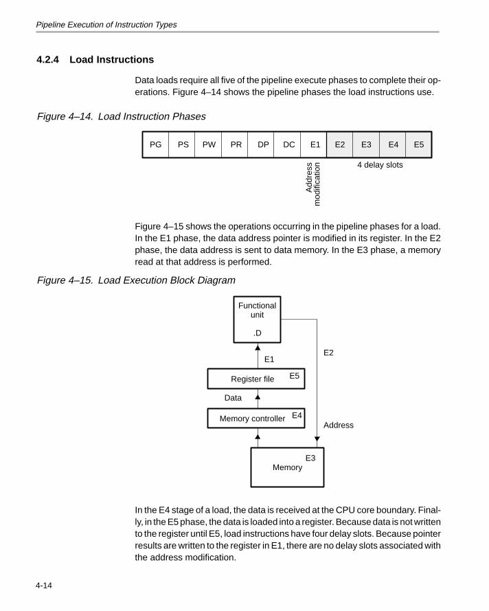
Pipeline Execution of Instruction Types
4-14
4.2.4 Load Instructions
Data loads require all five of the pipeline execute phases to complete their op-erations. Figure 4–14 shows the pipeline phases the load instructions use.
Figure 4–14. Load Instruction Phases
PG PS PW PR DP DC E1 E2 E3 E4 E5
4 delay slots
Add
ress
mod
ifica
tion
Figure 4–15 shows the operations occurring in the pipeline phases for a load.In the E1 phase, the data address pointer is modified in its register. In the E2phase, the data address is sent to data memory. In the E3 phase, a memoryread at that address is performed.
Figure 4–15. Load Execution Block Diagram
E5
Address
E3Memory
E2
E4Memory controller
Register file
E1
.D
Functionalunit
Data
In the E4 stage of a load, the data is received at the CPU core boundary. Final-ly, in the E5 phase, the data is loaded into a register. Because data is not writtento the register until E5, load instructions have four delay slots. Because pointerresults are written to the register in E1, there are no delay slots associated withthe address modification.

Pipeline Execution of Instruction Types
4-15 TMS320C62xx Pipeline
In the following code, pointer results are written to the A4 register in the firstexecute phase of the pipeline and data is written to the A3 register in the fifthexecute phase.
LDW .D1 *A4++,A3
Because a store takes three execute phases to write a value to memory anda load takes three execute phases to read from memory, a load following astore accesses the value placed in memory by that store in the cycle after thestore is completed. This is why the store is considered to have zero delay slots.
4.2.5 Branch Instructions
Although branch takes one execute phase, there are five delay slots betweenthe execution of the branch and execution of the target code. Figure 4–16shows the pipeline phases used by the branch instruction and branch targetcode. The delay slots are shaded.
Figure 4–16. Branch Instruction Phases
Branchtarget
PG PS PW PR DP DC E1
5 delay slots
PG PS PW PR DP DC E1

Pipeline Execution of Instruction Types
4-16
Figure 4–17 shows a branch execution block diagram. If a branch is in the E1phase of the pipeline (in the .S2 unit in the figure), its branch target is in thefetch packet that is in PG during that same cycle (shaded in the figure). Be-cause the branch target has to wait until it reaches the E1 phase to beginexecution, the branch takes five delay slots before the branch target codeexecutes.
Figure 4–17. Branch Execution Diagram
DP
PR
PW
PS
PG
3232323232323232
256
NOPMVSMPYHSMPYHSHRSHRLDWLDW
B
LDW
SUB
LDW
SMPY
SMPYH
SMPYH
SMPYH
SADD
SHR
SADD
SHR
STH
SADD
STH
SADD
BSUBSMPYSMPYHSADDSADDSTHSTH
MVKBSADDSADDSMPYSMPYH
DC LDWLDW
E1
.L1 .S1MVK
.D1.M1SMPY
.S2B
.D2SMPYH
.M2
Fetch
Decode
Execute
.L2

Performance Considerations
4-17 TMS320C62xx Pipeline
4.3 Performance ConsiderationsThe ’C62xx pipeline is most effective when it is kept as full as the algorithmsin the program allow it to be. It is useful to consider some situations that canaffect pipeline performance.
A fetch packet (FP) is a grouping of eight instructions. Each FP can be split intofrom one to eight execute packets (EPs). Each EP contains instructions thatexecute in parallel. Each instruction executes in an independent functionalunit. The effect on the pipeline of combinations of EPs that include varyingnumbers of parallel instructions, or just a single instruction that executes seri-ally with other code, is considered here.
In general, the number of execute packets in a single FP defines the flow ofinstructions through the pipeline. Another defining factor is the instructiontypes in the EP. Each type of instruction has a fixed number of execute cyclesthat determines when this instruction’s operations are complete. Section 4.3.2covers the effect of including a multicycle NOP in an individual EP.
Finally, the effect of the memory system on the operation of the pipeline is con-sidered. The access of program and data memory is discussed, along withmemory stalls.
4.3.1 Pipeline Operation With Multiple Execute Packets in a Fetch Packet
Again referring to Figure 4–6 on page 4-6, pipeline operation is shown witheight instructions in every fetch packet. Figure 4–18, however, shows the pipe-line operation with a fetch packet that contains multiple execute packets. Codefor Figure 4–18 might have this layout:
instruction A ; EP k FP n|| instruction B ;
instruction C ; EP k + 1 FP n|| instruction D || instruction E
instruction F ; EP k + 2 FP n|| instruction G || instruction H
instruction I ; EP k + 3 FP n + 1|| instruction J || instruction K || instruction L || instruction M || instruction N || instruction O || instruction P
... continuing with EPs k + 4 through k + 8, which haveeight instructions in parallel, like k + 3.

Performance Considerations
4-18
Figure 4–18. Pipeline Operation: Fetch Packets With Different Numbers of ExecutePackets
Clock cycleFetchpacket
(FP)
Executepacket
(EP) 1 2 3 4 5 6 7 8 9 10 11 12 13n k PG PS PW PR ÉÉÉDP DC E1 E2 E3 E4 E5
n k+1ÉÉÉÉDP DC E1 E2 E3 E4 E5
n k+2 ÉÉÉÉÉÉ
DP DC E1 E2 E3 E4 E5
n+1 k+3 PG PS PW PR DP DC E1 E2 E3 E4
n+2 k+4 PG PS PW Pipeline PR DP DC E1 E2 E3
n+3 k+5 PG PS stall PW PR DP DC E1 E2
n+4 k+6 PG PS PW PR DP DC E1
n+5 k+7 PG PS PW PR DP DC
n+6 k+8 PG PS PW PR DP
In Figure 4–18, fetch packet n, which contains three execute packets, isshown followed by six fetch packets (n + 1 through n + 6), each with oneexecute packet (containing eight parallel instructions). The first fetch packet(n) goes through the program fetch phases during cycles 1–4. During thesecycles, a program fetch phase is started for each of the fetch packets that fol-low.
In cycle 5, the program dispatch (DP) phase, the CPU scans the p-bits and de-tects that there are three execute packets (k through k + 2) in fetch packet n.This forces the pipeline to stall, which allows the DP phase to start for executepackets k + 1 and k + 2 in cycles 6 and 7. Once execute packet k + 2 is readyto move on to the DC phase (cycle 8), the pipeline stall is released.
The fetch packets n + 1 through n + 4 were all stalled so the CPU could havetime to perform the DP phase for each of the three execute packets(k through k + 2) in fetch packet n. Fetch packet n + 5 was also stalled in cycles6 and 7: it was not allowed to enter the PG phase until after the pipeline stallwas released in cycle 8. The pipeline continues operation as shown with fetchpackets n + 5 and n + 6 until another fetch packet containing multiple execu-tion packets enters the DP phase, or an interrupt occurs.
4.3.2 Multicycle NOPs
The NOP instruction has an optional operand, count, that allows you to issuea single instruction for multicycle NOPs. A NOP 2, for example, fills in extradelay slots for the instructions in its execute packet and for all previous executepackets. If a NOP 2 is in parallel with an MPY instruction, the MPY’s resultswill be available for use by instructions in the next execute packet.
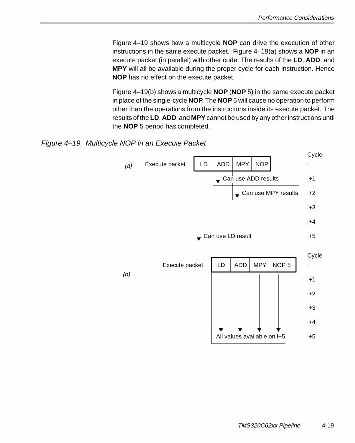
Performance Considerations
4-19 TMS320C62xx Pipeline
Figure 4–19 shows how a multicycle NOP can drive the execution of otherinstructions in the same execute packet. Figure 4–19(a) shows a NOP in anexecute packet (in parallel) with other code. The results of the LD, ADD, andMPY will all be available during the proper cycle for each instruction. HenceNOP has no effect on the execute packet.
Figure 4–19(b) shows a multicycle NOP (NOP 5) in the same execute packetin place of the single-cycle NOP. The NOP 5 will cause no operation to performother than the operations from the instructions inside its execute packet. Theresults of the LD, ADD, and MPY cannot be used by any other instructions untilthe NOP 5 period has completed.
Figure 4–19. Multicycle NOP in an Execute Packet
Execute packet
Cycle
i+5
i+4
i+3
i+2
i+1
i
Can use LD result
Can use MPY results
Can use ADD results
NOPMPYADDLD(a)
Execute packet
Cycle
i+5
i+4
i+3
i+2
i+1
i
All values available on i+5
NOP 5MPYADDLD
(b)

Performance Considerations
4-20
Figure 4–20 shows how a multicycle NOP can be affected by a branch. If thedelay slots of a branch finish while a multicycle NOP is still dispatching NOPsinto the pipeline, the branch overrides the multicycle NOP and the branch tar-get begins execution five delay slots after the branch was issued.
Figure 4–20. Branching and Multicycle NOPs
EP7Normal
Cycle #
11
10
9
8
7
6
5
4
3
2
1
Target
E1
DC
DP
PR
PW
PS
PG
Branch
E1
EP6
EP5
EP4
EP3
EP2
EP1
NOP5ADDMPYLD
EP without branch
EP without branch
. . .B
EP without branch
EP without branch
Branch will execute here
Pipeline phase
�
�
�
�
�
BranchEP7
See Figure 4–19(b)
† Delay slots of the branch
In one case, execute packet 1 (EP1) does not have a branch. The NOP 5 inEP6 will force the CPU to wait until cycle 11 to execute EP7.
In the other case, EP1 does have a branch. The delay slots of the branch coin-cide with cycles 2 through 6. Once the target code reaches E1 in cycle 7, itexecutes.

Performance Considerations
4-21 TMS320C62xx Pipeline
4.3.3 Memory Considerations
The ’C62xx has a memory configuration typical of a DSP, with programmemory in one physical space and data memory in another physical space.Data loads and program fetches have the same operation in the pipeline, theyjust use different phases to complete their operations. With both data loadsand program fetches, memory accesses are broken up into multiple phases.This enables the ’C62xx to access memory at a high speed. These phases areshown in Figure 4–21.
Figure 4–21. Pipeline Phases Used During Memory Accesses
Program memory accesses use these pipeline phases
Data load accesses use these pipeline phases
PG PS PW PR DP
E1 E2 E3 E4 E5
To understand the memory accesses, compare data loads and instructionfetches/dispatches. The comparison is valid because data loads and programfetches operate on internal memories of the same speed on the ’C62xx andperform the same types of operations (listed in Table 4–3) to accommodatethose memories. Table 4–3 shows the operation of program fetches pipelineversus the operation of a data load.
Table 4–3. Program Memory Accesses Versus Data Load Accesses
ÁÁÁÁÁÁÁÁÁÁÁÁÁÁÁÁÁÁÁÁÁÁÁÁÁÁÁÁÁÁÁÁÁÁÁÁÁÁÁÁÁÁÁÁÁÁÁÁÁÁÁÁÁÁÁÁÁÁÁÁÁÁÁÁ
Operation
ÁÁÁÁÁÁÁÁÁÁÁÁÁÁÁÁ
ProgramMemoryAccessPhase
ÁÁÁÁÁÁÁÁÁÁÁÁÁÁÁÁÁÁÁÁ
DataLoad
AccessPhase
ÁÁÁÁÁÁÁÁÁÁÁÁÁÁÁÁÁÁÁÁÁÁÁÁÁÁÁÁÁÁÁÁ
Compute address ÁÁÁÁÁÁÁÁ
PG ÁÁÁÁÁÁÁÁÁÁ
E1ÁÁÁÁÁÁÁÁÁÁÁÁÁÁÁÁÁÁÁÁÁÁÁÁÁÁÁÁÁÁÁÁ
Send address to memoryÁÁÁÁÁÁÁÁ
PSÁÁÁÁÁÁÁÁÁÁ
E2ÁÁÁÁÁÁÁÁÁÁÁÁÁÁÁÁÁÁÁÁÁÁÁÁÁÁÁÁÁÁÁÁÁÁÁÁÁÁÁÁÁÁÁÁÁÁÁÁ
Memory read/writeÁÁÁÁÁÁÁÁÁÁÁÁ
PWÁÁÁÁÁÁÁÁÁÁÁÁÁÁÁ
E3
ÁÁÁÁÁÁÁÁÁÁÁÁÁÁÁÁÁÁÁÁÁÁÁÁÁÁÁÁÁÁÁÁÁÁÁÁÁÁÁÁÁÁÁÁÁÁÁÁ
Program memory: receive fetch packet at CPU boundaryData load: receive data at CPU boundary
ÁÁÁÁÁÁÁÁÁÁÁÁ
PR ÁÁÁÁÁÁÁÁÁÁÁÁÁÁÁ
E4
ÁÁÁÁÁÁÁÁÁÁÁÁÁÁÁÁÁÁÁÁÁÁÁÁÁÁÁÁÁÁÁÁÁÁÁÁÁÁÁÁÁÁÁÁÁÁÁÁ
Program memory: send instruction to functional unitsData load: send data to register
ÁÁÁÁÁÁÁÁÁÁÁÁ
DP ÁÁÁÁÁÁÁÁÁÁÁÁÁÁÁ
E5
Depending on the type of memory and the time required to complete an ac-cess, the pipeline may stall to ensure proper coordination of data and instruc-tions. This is discussed in section 4.3.3.1, Memory Stalls.

Performance Considerations
4-22
In the instance where multiple accesses are made to a single ported memory,the pipeline will stall to allow the extra access to occur. This is called a memorybank hit and is discussed in section 4.3.3.2, Memory Bank Hits.
4.3.3.1 Memory Stalls
A memory stall occurs when memory is not ready to respond to an access fromthe CPU. This access occurs during the PW phase for a program memory ac-cess and during the E3 phase for a data memory access. The memory stallcauses all of the pipeline phases to lengthen beyond a single clock cycle, caus-ing execution to take additional clock cycles to finish. The results of the pro-gram execution are identical whether a stall occurs or not. Figure 4–22 illus-trates this point.
Figure 4–22. Program and Data Memory StallsÁÁÁÁÁÁÁÁÁÁÁÁÁÁÁÁÁÁÁÁÁÁÁÁÁÁÁÁÁÁÁÁÁÁÁÁÁÁÁÁÁÁÁÁÁÁÁÁÁÁÁÁÁÁÁÁÁÁÁÁClock cycleÁÁÁÁÁÁÁÁÁÁÁÁÁÁÁÁ
Fetchpacket
(FP)
ÁÁÁÁÁÁÁÁ
1
ÁÁÁÁÁÁÁÁÁÁÁÁ
2
ÁÁÁÁÁÁÁÁÁÁÁÁ
3
ÁÁÁÁÁÁÁÁ
4
ÁÁÁÁÁÁÁÁÁÁÁÁ
5
ÁÁÁÁÁÁÁÁÁÁÁÁ
6
ÁÁÁÁÁÁÁÁ
7 8 9
ÁÁÁÁÁÁÁÁ
10
ÁÁÁÁÁÁÁÁÁÁÁÁ
11
ÁÁÁÁÁÁÁÁÁÁÁÁ
12
ÁÁÁÁÁÁÁÁ
13
ÁÁÁÁÁÁÁÁÁÁÁÁ
14
ÁÁÁÁÁÁÁÁ
15
ÁÁÁÁÁÁÁÁÁÁÁÁ
16ÁÁÁÁÁÁÁÁn PG PS PW PR DP DC E1 E2
ÉÉÉÉÉÉE3 E4 E5ÁÁÁÁ
ÁÁÁÁn+1ÁÁÁÁ
PG PS PW PR DP DC E1 E2 E3 E4ÁÁÁÁÁÁÁÁ
n+2 ÁÁÁÁÁÁÁÁÁÁ
PG PS PW PR DP Program DC E1 E2 E3
ÁÁÁÁÁÁÁÁ
n+3 ÁÁÁÁÁÁÁÁÁÁÁÁÁÁÁÁ
PG PS PW PR memory stall DP DC Data E1 E2
ÁÁÁÁÁÁÁÁ
n+4 ÁÁÁÁÁÁÁÁÁÁÁÁÁÁÁÁÁÁÁÁ
PG PS ÉÉÉÉ
PW PR DP memory stall DC E1
ÁÁÁÁn+5 ÁÁÁÁÁÁÁÁÁÁÁÁÁPG PS PW PR DP DCÁÁÁÁÁÁÁÁ
n+6ÁÁÁÁÁÁÁÁÁÁÁÁÁÁÁÁÁÁÁÁÁÁÁÁÁÁÁÁÁÁÁÁ
PG PS PW PR DPÁÁÁÁÁÁÁÁ
n+7 ÁÁÁÁÁÁÁÁÁÁÁÁÁÁÁÁÁÁÁÁÁÁÁÁÁÁÁÁÁÁÁÁÁÁÁÁ
PG PS PW PR
ÁÁÁÁÁÁÁÁ
n+8 ÁÁÁÁÁÁÁÁÁÁÁÁÁÁÁÁÁÁÁÁÁÁÁÁÁÁÁÁÁÁÁÁÁÁÁÁ
ÁÁÁÁ
PG PS PW
ÁÁÁÁÁÁÁÁ
n+9 ÁÁÁÁÁÁÁÁÁÁÁÁÁÁÁÁÁÁÁÁÁÁÁÁÁÁÁÁÁÁÁÁÁÁÁÁ
ÁÁÁÁÁÁÁÁÁÁÁÁÁÁÁÁÁÁÁÁÁÁÁÁÁÁ
PG PS
ÁÁÁÁn+10ÁÁÁÁÁÁÁÁÁÁÁÁÁÁÁÁÁÁ ÁÁÁÁÁÁÁÁÁÁÁÁÁÁÁ PG

Performance Considerations
4-23 TMS320C62xx Pipeline
4.3.3.2 Memory Bank Hits
Most ’C62xx devices use an interleaved memory bank scheme, as shown inFigure 4–23. Each number in the diagram represents a byte address. A loadbyte (LDB ) instruction from address 0 loads byte 0 in bank 0. A load halfword(LDH) from address 0 loads the halfword value in bytes 0 and 1, which are alsoin bank 0. An LDW from address 0 loads bytes 0 through 3 in banks 0 and 1.
Figure 4–23. 4-Bank Interleaved Memory
6 7
14 15
8N + 6 8N + 7
Bank 3Bank 2
8N + 58N + 4
1312
542 3
10 11
8N + 2 8N + 3
Bank 1Bank 0
8N + 18N
98
10
Because each of these banks is single-ported memory, only one access toeach bank is allowed per cycle. Two accesses to a single bank in a given cycleresult in a memory stall that halts all pipeline operation for one cycle, while thesecond value is read from memory. Two memory operations per cycle areallowed without any stall, as long as they do not access the same bank.
Consider the code in Example 4–3. Because both loads are trying to accessthe same bank at the same time, one load must wait. The first LDW accessesbank 0 on cycle i + 2 (in the E3 phase) and the second LDW accesses bank0 on cycle i + 3 (in the E3 phase). See Table 4–4 for identification of cycles andphases. The E4 phase for both LDW instructions is in cycle i + 4. To eliminatethis extra phase, the loads must access data from different banks (B4 addresswould need to be in bank 1). For more information on programming topics, seethe TMS320C62xx Programmer’s Guide.
Example 4–3. Load From Memory Banks
LDW .D1 *A4++,A5 ; load 1, A4 address is in bank 0|| LDW .D2 *B4++,B5 ; load 2, B4 address is in bank 0
Table 4–4. Loads in Pipeline From Example 4–3
i i +1 i +2 i +3 i +4 i +5
LDW .D1Bank 0
E1 E2 E3 * E4 E5
LDW .D2Bank 0
E1 E2 * E3 E4 E5

Performance Considerations
4-24
For devices that have more than one memory space (see Figure 4–24), anaccess to bank 0 in one space does not interfere with an access to bank 0 inanother memory space, and no pipeline stall occurs.
Figure 4–24. 4-Bank Interleaved Memory With Two Memory Spaces
6 7
14 15
8N + 6 8N + 7
Bank 3Bank 2
8N + 58N + 4
1312
542 3
10 11
8N + 2 8N + 3
Bank 1Bank 0
8N + 18N
98
10
8M + 6 8M + 78M + 58M + 48M + 2 8M + 38M + 18M
Memory space 0
Memory space 1
Bank 3Bank 2Bank 1Bank 0
The internal memory of the ’C62xx family varies from device to device. Seethe TMS320C62xx Peripherals Reference Guide to determine the memoryspaces in your particular device.

5-1
Interrupts
This chapter describes CPU interrupts, including reset and the nonmaskableinterrupt (NMI). It details the related CPU control registers and their functionsin controlling interrupts. It also describes interrupt processing, the method theCPU uses to detect automatically the presence of interrupts and divert pro-gram execution flow to your interrupt service code. Finally, the chapter de-scribes the programming implications of interrupts.
Topic Page
5.1 Overview of Interrupts 5-2. . . . . . . . . . . . . . . . . . . . . . . . . . . . . . . . . . . . . . . . .
5.2 Globally Enabling and Disabling Interrupts(Control Status Register–CSR) 5-11. . . . . . . . . . . . . . . . . . . . . . . . . . . . . . . .
5.3 Individual Interrupt Control 5-13. . . . . . . . . . . . . . . . . . . . . . . . . . . . . . . . . . .
5.4 Interrupt Detection and Processing 5-18. . . . . . . . . . . . . . . . . . . . . . . . . . . .
5.5 Performance Considerations 5-23. . . . . . . . . . . . . . . . . . . . . . . . . . . . . . . . . .
5.6 Programming Considerations 5-24. . . . . . . . . . . . . . . . . . . . . . . . . . . . . . . . .
Chapter 5

Overview of Interrupts
5-2
5.1 Overview of Interrupts
Typically, DSPs work in an environment that contains multiple externalasynchronous events. These events require tasks to be performed by the DSPwhen they occur. An interrupt is an event that stops the current process in theCPU so that the CPU can attend to the task needing completion because ofthe event. These interrupt sources can be on chip or off chip, such as timers,analog-to-digital converters, or other peripherals.
Servicing an interrupt involves saving the context of the current process, com-pleting the interrupt task, restoring the registers and the process context, andresuming the original process. There are eight registers that control servicinginterrupts.
An appropriate transition on an interrupt pin sets the pending status of the in-terrupt within the interrupt flag register (IFR). If the interrupt is properly en-abled, the CPU begins processing the interrupt and redirecting program flowto the interrupt service routine.
5.1.1 Types of Interrupts and Signals Used
There are three types of interrupts on the ’C62xx CPU. These three types aredifferentiated by their priorities, as shown in Table 5–1. The reset interrupt hasthe highest priority and corresponds to the RESET signal. The nonmaskableinterrupt is the interrupt of second highest priority and corresponds to the NMIsignal. The lowest priority interrupts are interrupts 4–15. They correspond tothe INT4–INT15 signals. RESET, NMI, and some of the INT4–INT15 signalsare mapped to pins on ’C62xx devices. Some of the INT4–INT15 interrupt sig-nals are used by internal peripherals and some may be unavailable or can beused under software control. Check your data sheet to see your device’s inter-rupt specifications.

Overview of Interrupts
5-3Interrupts
Table 5–1. Interrupt Priorities ÁÁÁÁÁÁÁÁÁÁÁÁÁÁÁÁÁÁÁÁÁPriority
ÁÁÁÁÁÁÁÁÁÁÁÁÁÁÁÁÁÁÁÁÁ
InterruptNameÁÁÁÁÁÁÁ
ÁÁÁÁÁÁÁHighestÁÁÁÁÁÁÁÁÁÁÁÁÁÁResetÁÁÁÁÁÁÁ
ÁÁÁÁÁÁÁÁÁÁÁÁÁÁÁÁÁÁÁÁÁ
NMIÁÁÁÁÁÁÁÁÁÁÁÁÁÁ
ÁÁÁÁÁÁÁÁÁÁÁÁÁÁ
INT4ÁÁÁÁÁÁÁÁÁÁÁÁÁÁ
ÁÁÁÁÁÁÁÁÁÁÁÁÁÁ
INT5
ÁÁÁÁÁÁÁÁÁÁÁÁÁÁ
ÁÁÁÁÁÁÁÁÁÁÁÁÁÁ
INT6
ÁÁÁÁÁÁÁÁÁÁÁÁÁÁINT7ÁÁÁÁÁÁÁÁÁÁÁÁÁÁ
ÁÁÁÁÁÁÁÁÁÁÁÁÁÁINT8ÁÁÁÁÁÁÁ
ÁÁÁÁÁÁÁÁÁÁÁÁÁÁÁÁÁÁÁÁÁ
INT9ÁÁÁÁÁÁÁÁÁÁÁÁÁÁ
ÁÁÁÁÁÁÁÁÁÁÁÁÁÁ
INT10ÁÁÁÁÁÁÁÁÁÁÁÁÁÁ
ÁÁÁÁÁÁÁÁÁÁÁÁÁÁ
INT11
ÁÁÁÁÁÁÁÁÁÁÁÁÁÁ
ÁÁÁÁÁÁÁÁÁÁÁÁÁÁ
INT12ÁÁÁÁÁÁÁÁÁÁÁÁÁÁ
ÁÁÁÁÁÁÁÁÁÁÁÁÁÁINT13ÁÁÁÁÁÁÁ
ÁÁÁÁÁÁÁÁÁÁÁÁÁÁÁÁÁÁÁÁÁ
INT14ÁÁÁÁÁÁÁÁÁÁÁÁÁÁ
Lowest ÁÁÁÁÁÁÁÁÁÁÁÁÁÁ
INT15
5.1.1.1 Reset (RESET)
Reset is the highest priority interrupt and is used to halt the CPU and returnit to a known state. The reset interrupt is unique in a number of ways:
� RESET is an active-low signal. All other interrupts are active-high signals.
� RESET must be held low for 10 clock cycles before it goes high again toreinitialize the CPU properly.
� The instruction execution in progress is aborted and all registers are re-turned to their default states.
� The reset interrupt service fetch packet must be located at address 0.
� RESET is not affected by branches.
5.1.1.2 Nonmaskable Interrupt (NMI)
NMI is the second-highest priority interrupt and is generally used to alert theCPU of a serious hardware problem such as imminent power failure.
For NMI processing to occur, the nonmaskable interrupt enable (NMIE) bit inthe interrupt enable register must be set to 1. If NMIE is set to 1, the only condi-tion that can prevent NMI processing is if the NMI occurs during the delay slotsof a branch (whether the branch is taken or not).
NMIE is cleared to 0 at reset to prevent interruption of the reset. It is clearedat the occurrence of an NMI to prevent another NMI from being processed. You

Overview of Interrupts
5-4
cannot manually clear NMIE, but you can set NMIE to allow nested NMIs.While NMI is cleared, all maskable interrupts (INT4–INT15) are disabled.
5.1.1.3 Maskable Interrupts (INT4–INT15)
The ’C62xx CPU has twelve interrupts that are maskable. These have lowerpriority than the NMI and reset interrupts. These interrupts can be associatedwith external devices, on-chip peripherals, software control, or not be avail-able.
Assuming that a maskable interrupt does not occur during the delay slots ofa branch (this includes conditional branches that do not complete executiondue to a false condition), the following conditions must be met to process amaskable interrupt:
� The global interrupt enable bit (GIE) bit in the control status register (CSR) isset to1.
� The NMIE bit in the interrupt enable register (IER) is set to1.
� The corresponding interrupt enable (IE) bit in the IER is set to1.
� The corresponding interrupt occurs, which sets the corresponding bit inthe IFR to 1 and there are no higher priority interrupt flag (IF) bits set in theIFR.
5.1.1.4 Interrupt Acknowledgment (IACK and INUMx)
The IACK and INUMx signals alert hardware external to the ’C62xx that an in-terrupt has occurred and is being processed. The IACK signal indicates thatthe CPU has begun processing an interrupt. The INUMx signals (INUM3–INUM0) indicate the number of the interrupt (bit position in the IFR) that is be-ing processed.
For example:
INUM3 = 0 (MSB)INUM2 = 1INUM1 = 1INUM0 = 1 (LSB)
Together, these signals provide the 4-bit value 0111, indicating INT7 is beingprocessed.

Overview of Interrupts
5-5Interrupts
5.1.2 Interrupt Service Table (IST)
When the CPU begins processing an interrupt, it references the interrupt ser-vice table (IST). The IST is a table of fetch packets that contain code for servic-ing the interrupts. The IST consists of 16 consecutive fetch packets. Each in-terrupt service fetch packet contains eight instructions. A simple interrupt ser-vice routine may fit in an individual fetch packet.
The addresses and contents of the IST are shown in Figure 5–1. Becauseeach fetch packet contains eight 32-bit instruction words (or 32 bytes), eachaddress in the table is incremented by 32 bytes (20h) from the one adjacentto it.
Figure 5–1. Interrupt Service Table
Interrupt service table(IST)
000h
020h
040h
060h
080h
0A0h
0C0h
0E0h
100h
120h
140h
160h
180h
1A0h
1C0h
1E0h
Program memory
RESET ISFP
NMI ISFP
Reserved
Reserved
INT4 ISFP
INT5 ISFP
INT6 ISFP
INT7 ISFP
INT8 ISFP
INT9 ISFP
INT10 ISFP
INT11 ISFP
INT12 ISFP
INT13 ISFP
INT14 ISFP
INT15 ISFP

Overview of Interrupts
5-6
5.1.2.1 Interrupt Service Fetch Packet (ISFP)
An ISFP is a fetch packet used to service an interrupt. Figure 5–2 shows anISFP that contains an interrupt service routine small enough to fit in a singlefetch packet (FP). To branch back to the main program, the FP contains abranch to the interrupt return pointer instruction (B IRP). This is followed by aNOP 5 instruction to allow the branch target to reach the execution stage ofthe pipeline.
Note:
If the NOP 5 was not in the routine, the CPU would execute the next fiveexecute packets that are associated with the next ISFP.
Figure 5–2. Interrupt Service Fetch Packet
Instr3
Interrupt service table(IST)
Instr2
Instr4
Instr5
Instr6
B IRP
NOP 5
ISFP for INT6
000h
020h
040h
060h
080h
0A0h
0C0h
0E0h
100h
120h
140h
160h
180h
1A0h
1C0h
1E0h
0C0h
0C4h
0C8h
0CCh
0D0h
0D4h
0D8h
0DCh
The interrupt service rou-tine for INT6 is short
enough to be containedin a single fetch packet.
Program memory
RESET ISFP
NMI ISFP
Reserved
Reserved
INT4 ISFP
INT5 ISFP
INT6 ISFP
INT7 ISFP
INT8 ISFP
INT9 ISFP
INT10 ISFP
INT11 ISFP
INT12 ISFP
INT13 ISFP
INT14 ISFP
INT15 ISFP
Instr1

Overview of Interrupts
5-7Interrupts
If the interrupt service routine for an interrupt is too large to fit in a single FP,a branch to the location of additional interrupt service routine code is required.Figure 5–3 shows that the interrupt service routine for INT4 was too large fora single FP, and a branch to memory location 1234h is required to completethe interrupt service routine.
Figure 5–3. IST With Branch to Additional Interrupt Service Code Located Outside the IST
IST
RESET ISFP
NMI ISFP
Reserved
Reserved
INT4 ISFP
INT5 ISFP
INT6 ISFP
INT7 ISFP
INT8 ISFP
INT9 ISFP
INT10 ISFP
INT11 ISFP
INT12 ISFP
INT13 ISFP
INT14 ISFP
INT15 ISFP
Additional ISFP for INT4
1220h
The interrupt service routinefor INT4 includes this
7-instruction extension ofthe interrupt ISFP. Instr1
Instr2
B 1234h
Instr4
Instr5
Instr6
Instr7
Instr8
ISFP for INT4
080h
084h
088h
08Ch
090h
094h
098h
09Ch
Program memory
–
–
–
–
–
Instr9
Instr11
1224h
1228h
122Ch
1230h
1234h
1238h
123Ch
B IRP
000h
020h
040h
060h
080h
0A0h
0C0h
0E0h
100h
120h
140h
160h
180h
1A0h
1C0h
1E0h
Additional ISFP for INT4
1240h Instr12
Instr13
Instr14
Instr15
–
–
–
1244h
1248h
124Ch
1250h
1254h
1258h
125Ch
–
Note:
The instruction B 1234h branches into the middle of a fetch packet (at 1220h)and processes code starting at address 1234h. The CPU ignores code fromaddress 1220–1230h, even if it is in parallel to code at address 1234h.

Overview of Interrupts
5-8
5.1.2.2 Interrupt Service Table Pointer Register (ISTP)
The interrupt service table pointer (ISTP) register is used to locate the interruptservice routine. One field, ISTB identifies the base portion of the address ofthe IST; another field, HPEINT, identifies the specific interrupt and locates thespecific fetch packet within the IST. Figure 5–4 shows the fields of the ISTP.Table 5–2 describes the fields and how they are used.
Figure 5–4. Interrupt Service Table Pointer (ISTP)
31 0
R, +0
0
R, W, +0
10
HPEINTISTB 0000
59
Legend : R Readable by the MVC instructionW Writeable by the MVC instruction+0 Value is cleared at reset
Table 5–2. ISTP Fields
ÁÁÁÁÁÁÁÁÁ
BitsÁÁÁÁÁÁÁÁÁÁÁÁ
FieldName
ÁÁÁÁÁÁÁÁÁÁÁÁÁÁÁÁÁÁÁÁÁÁÁÁÁÁÁÁÁÁÁÁÁÁÁÁÁÁÁÁÁÁÁÁÁÁÁÁÁÁÁÁÁÁÁÁÁÁÁÁÁÁÁÁÁÁÁÁÁÁÁÁÁÁÁ
Description
ÁÁÁÁÁÁ
0–4ÁÁÁÁÁÁÁÁ
ÁÁÁÁÁÁÁÁÁÁÁÁÁÁÁÁÁÁÁÁÁÁÁÁÁÁÁÁÁÁÁÁÁÁÁÁÁÁÁÁÁÁÁÁÁÁÁÁÁÁ
Set to 0 (fetch packets must be aligned on 8-word (32-byte) boundaries).
ÁÁÁÁÁÁÁÁÁÁÁÁÁÁÁ
5–9ÁÁÁÁÁÁÁÁÁÁÁÁÁÁÁÁÁÁÁÁ
HPEINTÁÁÁÁÁÁÁÁÁÁÁÁÁÁÁÁÁÁÁÁÁÁÁÁÁÁÁÁÁÁÁÁÁÁÁÁÁÁÁÁÁÁÁÁÁÁÁÁÁÁÁÁÁÁÁÁÁÁÁÁÁÁÁÁÁÁÁÁÁÁÁÁÁÁÁÁÁÁÁÁÁÁÁÁÁÁÁÁÁÁÁÁÁÁÁÁÁÁÁÁÁÁÁÁÁÁÁÁÁÁÁÁÁÁÁÁÁÁÁÁÁÁÁÁÁ
Highest priority enabled interrupt. This field gives the number (related bit position in the IFR)of the highest priority interrupt (as defined in Table 5–1) that is enabled by its bit in the IER.Thus, the ISTP can be used for manual branches to the highest priority enabled interrupt.If no interrupt is pending and enabled, HPEINT contains the value 00000b. The correspond-ing interrupt need not be enabled by NMIE (unless it is NMI) or by GIE.
ÁÁÁÁÁÁÁÁÁÁÁÁ
10–31ÁÁÁÁÁÁÁÁÁÁÁÁÁÁÁÁ
ISTBÁÁÁÁÁÁÁÁÁÁÁÁÁÁÁÁÁÁÁÁÁÁÁÁÁÁÁÁÁÁÁÁÁÁÁÁÁÁÁÁÁÁÁÁÁÁÁÁÁÁÁÁÁÁÁÁÁÁÁÁÁÁÁÁÁÁÁÁÁÁÁÁÁÁÁÁÁÁÁÁÁÁÁÁÁÁÁÁÁÁÁÁÁÁÁÁÁÁÁÁ
Interrupt service table base portion of the IST address. This field is set to 0 on reset. Thus,upon startup the IST must reside at address 0. After reset, you can relocate the IST by writ-ing a new value to ISTB. If relocated, the first ISFP (corresponding to RESET) is neverexecuted via interrupt processing, because reset sets the ISTB to 0. See Example 5–1.

Overview of Interrupts
5-9Interrupts
The reset fetch packet must be located at address 0, but the rest of the IST canbe at any program memory location that is on a 256-word boundary. The loca-tion of the IST is determined by the interrupt service table base (ISTB).Example 5–1 shows the relationship of the ISTB to the table location.
Example 5–1. Relocation of Interrupt Service Table
IST
NMI ISFP
Reserved
Reserved
INT4 ISFP
INT5 ISFP
INT6 ISFP
INT7 ISFP
INT8 ISFP
INT9 ISFP
INT10 ISFP
INT11 ISFP
INT12 ISFP
INT13 ISFP
INT14 ISFP
INT15 ISFP
0
820h
840h
860h
880h
8A0h
8C0h
8E0h
900h
920h
940h
96h0
980h
9A0h
9C0h
9E0h
Program memory
800h
RESET ISFP
1) Copy the IST, located between 0h and 200h, to the memory loca-tion between 800h and A00h.
2) Write 800h to the ISTP register: MVK 800h, A2MVC A2, ISTP
ISTP = 800h = 1000 0000 0000b
RESET ISFP
Assume: IFR = BBC0h = 1011 1011 1100 0000b IER = 1230h = 0001 0010 0011 0001b2 enabled interrupts pending: INT9 and INT12
The 1s in the IFR indicate pending interrupts; the 1s in the IERindicate the interrupts that are enabled. INT9 has a higher priority than INT12, so HPEINT is encoded with the value for INT9, 01001b.
HPEINT corresponds to bits 9–5 of the ISTP:ISTP = 1001 0010 0000b = 920h = address of INT9
(b) How the ISTP directs the CPU to the appropriate ISFP in therelocated IST
(a) Relocating the IST to 800h

Overview of Interrupts
5-10
5.1.3 Summary of Interrupt Control Registers
Table 5–3 lists the eight interrupt control registers on the ’C62xx devices. Thecontrol status register (CSR) and the interrupt enable register (IER) enable ordisable interrupt processing. The interrupt flag register (IFR) identifies pendinginterrupts. The interrupt set (ISR) and interrupt clear (ICR) registers can beused in manual interrupt processing.
There are three pointer registers. ISTP points to the interrupt service table.NRP and IRP are the return pointers used when returning from a nonmaskableor a maskable interrupt, respectively. More information on all the registers canbe found at the locations listed in the table.
Table 5–3. Interrupt Control Registers
Abbreviation Name DescriptionPage
Number
CSR Control status register Allows you to globally set or disable interrupts 5-11
IER Interrupt enable register Allows you to enable interrupts 5-13
IFR Interrupt flag register Shows the status of interrupts 5-14
ISR Interrupt set register Allows you to set flags in the IFR manually 5-14
ICR Interrupt clear register Allows you to clear flags in the IFR manually 5-14
ISTP Interrupt service table pointer Pointer to the beginning of the interrupt servicetable
5-8
NRP Nonmaskable interrupt returnpointer
Contains the return address used on return froma nonmaskable interrupt. This return is accom-plished via the B NRP instruction.
5-16
IRP Interrupt return pointer Contains the return address used on return froma maskable interrupt. This return is accom-plished via the B IRP instruction.
5-17

Globally Enabling and Disabling Interrupts
5-11Interrupts
5.2 Globally Enabling and Disabling Interrupts (Control Status Register–CSR)
The control status register (CSR) contains two fields that control interrupts:GIE and PGIE, as shown in Figure 5–5. The other fields of the registers serveother purposes and are discussed in section 2.4 on page 2-9.
Figure 5–5. Control Status Register (CSR)31 24
CPU ID
1623
Revision ID
R
15
PWRD SAT EN PCC DCC
10 9 8 7 5 4 2 1 0
PGIE GIE
R, W, +0 R, +x R, W, +0R, C, +0
Legend : R Readable by the MVC instructionW Writeable by the MVC instruction+x Value undefined after reset+0 Value is zero after resetC Clearable using the MVC instruction
Table 5–4. CSR Interrupt Control Field Descriptions
BitFieldName Description
0 GIE Global interrupt enable; globally enables or disables allmaskable interrupts.GIE = 1 maskable interrupts globally enabledGIE = 0, maskable interrupts globally disabled
1 PGIE Previous GIE; saves the value of GIE when an interrupt istaken. This value is used on return from an interrupt.
The global interrupt enable (GIE) allows you to enable or disable all maskableinterrupts by controlling the value of a single bit. GIE is bit 0 of the control statusregister (CSR).
� GIE = 1 enables the maskable interrupts so that they are processed.� GIE = 0 disables the maskable interrupts so that they are not processed.
Bit 1 of the CSR is PGIE and contains the previous value of GIE. During pro-cessing of a maskable interrupt, PGIE is loaded with GIE and GIE is cleared.GIE is cleared during a maskable interrupt to keep another maskable interruptfrom occurring before the device state has been saved. Upon return from aninterrupt, by way of the B IRP instruction, the PGIE value is copied back to GIEand remains unchanged. The purpose of PGIE is to allow proper clearing ofGIE when an interrupt has already been detected for processing.
Globally Enabling and Disabling Interrupts (Control Status Register–CSR)

Globally Enabling and Disabling Interrupts
5-12
Suppose the CPU begins processing an interrupt. Just as the interrupt proces-sing begins, GIE is being cleared by you writing a 0 to bit 0 of the CSR with theMVC instruction. GIE is cleared by the MVC instruction prior to being copiedto PGIE. Upon returning from the interrupt, PGIE is copied back to GIE, result-ing in GIE being cleared as directed by your code.
Example 5–2 shows how to disable maskable interrupts globally andExample 5–3 shows how to enable maskable interrupts globally.
Example 5–2. Code Sequence to Disable Maskable Interrupts Globally
MVC .S2 CSR,B0 ; get CSRAND .S2 -2,B0,B0 ; get ready to clear GIEMVC .S2 B0,CSR ; clear GIE
Example 5–3. Code Sequence to Enable Maskable Interrupts Globally
MVC .S2 CSR,B0 ; get CSROR .S2 1,B0,B0 ; get ready to set GIEMVC .S2 B0,CSR ; set GIE
Globally Enabling and Diasable Interrupts (Control Status Register–CSR)

Individual Interrupt Control
5-13Interrupts
5.3 Individual Interrupt Control
Servicing interrupts effectively requires individual control of all three types ofinterrupts: reset, nonmaskable, and maskable. Enabling and disabling individ-ual interrupts is done with the interrupt enable register (IER). The status ofpending interrupts is stored in the interrupt flag register (IFR). Manual interruptprocessing can be accomplished through the use of the interrupt set register(ISR) and interrupt clear register (ICR). The interrupt return pointers restorecontext after servicing nonmaskable and maskable interrupts.
5.3.1 Enabling and Disabling Interrupts (Interrupt Enable Register–IER)
You can enable and disable individual interrupts by setting and clearing bitsin the IER that correspond to the individual interrupts. An interrupt can triggerinterrupt processing only if the corresponding bit in the IER is set. Bit 0, corre-sponding to reset, is not writeable and is always read as 1, so the reset inter-rupt is always enabled. You cannot disable the reset interrupt. Bits IE4–IE15can be written as 1 or 0, enabling or disabling the associated interrupt, respec-tively. The IER is shown in Figure 5–6.
Figure 5–6. Interrupt Enable Register (IER)31 16
Reserved
15 0
IE15 IE14 IE13 IE12 IE11 IE10 IE9 IE8 IE7 IE6 IE5 IE4
R, W, +0
NMIE 1
R, +1
rsv rsv
Legend : R = Readable by the MVC instructionW = Writeable by the MVC instructionrsv = Reserved+1 = Value after reset+0 = Value after reset
When NMIE = 0, all nonreset interrupts are disabled, preventing interruptionof an NMI. NMIE is cleared at reset to prevent any interruption of processorinitialization until you enable NMI. After reset, you must set NMIE to enable theNMI and to allow INT15–INT4 to be enabled by GIE and the appropriate IERbit. You cannot manually clear the NMIE; the bit is unaffected by a write of 0.NMIE is also cleared by the occurrence of an NMI. If cleared, NMIE is set onlyby completing a B NRP instruction or by a write of 1 to NMIE. Example 5–4 andExample 5–5 show code for enabling and disabling individual interrupts, re-spectively.

Individual Interrupt Control
5-14
Example 5–4. Code Sequence to Enable an Individual Interrupt–INT9MVK.S2 200h,B1 ; set bit 9MVC.S2 IER,B0 ; get IEROR .S2 B1,B0,B0 ; get ready to set IE9MVC.S2 B0,IER ; set bit 9 in IER
Example 5–5. Code Sequence to Disable an Individual Interrupt–INT9MVK.S2 FDFFh,B1 ; clear bit 9MVC.S2 IER,B0AND.S2 B1,B0,B0 ; get ready to clear IE9MVC.S2 B0,IER ; clear bit 9 in IER
5.3.2 Status of, Setting, and Clearing Interrupts (Interrupt Flag, Set, and Clear Registers – IFR, ISR, ICR)
The interrupt flag register (IFR) contains the status of INT4–INT15 and NMI.Each interrupt’s corresponding bit in the IFR is set to 1 when that interrupt oc-curs; otherwise, the bits have a value of 0. If you want to check the status ofinterrupts, use the MVC instruction to read the IFR. Figure 5–7 shows the IFR.
Figure 5–7. Interrupt Flag Register (IFR)31 16
Reserved
R, +0
15 0
IF15 IF14 IF13 IF12 IF11 IF10 IF9 IF8 IF7 IF6 IF5 IF4 rsv rsv NMIF 0
R, +0
Legend : R = Readable by the MVC instruction+0 = Cleared at resetrsv = Reserved
The interrupt set register (ISR) and interrupt clear register (ICR) allow you toset or clear maskable interrupts manually in the IFR. Writing a 1 to IS4–IS15of the ISR causes the corresponding interrupt flag to be set in the IFR. Similar-ly, writing a 1 to a bit of the ICR causes the corresponding interrupt flag to becleared. Writing a 0 to any bit of either the ISR or the ICR has no effect. Incom-ing interrupts have priority and override any write to the ICR. You cannot setor clear any bit in the ISR or ICR to affect NMI or reset.
Note:
Any write to the ISR or ICR (by the MVC instruction) effectively has one delayslot because the results cannot be read (by the MVC instruction) in the IFRuntil two cycles after the write to the ISR or ICR.
Any write to the ICR is ignored by a simultaneous write to the same bit in theISR.

Individual Interrupt Control
5-15Interrupts
Figure 5–8. Interrupt Set Register (ISR)
31 16
Reserved
15 0
IS15 IS14 IS13 IS12 IS11 IS10 IS9 IS8 IS7 IS6 IS5 IS4
W
rsv rsv rsv rsv
Legend : W = Writeable by the MVC instructionrsv = Reserved
Figure 5–9. Interrupt Clear Register (ICR)
31 16Reserved
15 0IC15 IC14 IC13 IC12 IC11 IC10 IC9 IC8 IC7 IC6 IC5 IC4 rsv rsvrsv rsv
W
Legend : W = Writeable by the MVC instructionrsv = Reserved
Example 5–6 and Example 5–7 show code examples to set and clear individu-al interrupts.
Example 5–6. Code to Set an Individual Interrupt (INT6) and Read the Flag Register
MVK.S2 40h,B3MVC.S2 B3,ISRNOPMVC.S2 IFR,B4
Example 5–7. Code to Clear an Individual Interrupt (INT6) and Read the Flag Register
MVK.S2 40h,B3MVC.S2 B3,ICRNOPMVC.S2 IFR,B4

Individual Interrupt Control
5-16
5.3.3 Returning From Interrupt Servicing
After RESET goes high, the control registers are brought to a known value andprogram execution begins at address 0h. After nonmaskable and maskableinterrupt servicing, use a branch to the corresponding return pointer registerto continue the previous program execution.
5.3.3.1 CPU State After RESET
After RESET, the control registers and bits will contain the corresponding val-ues:� AMR, ISR, ICR, IFR, and ISTP = 0h� IER = 1h� IRP and NRP = undefined� Bits 15–0 of the CSR = 100h in little endian mode, 000h in big endian mode
5.3.3.2 Returning From Nonmaskable Interrupts (NMI Return Pointer Register–NRP)
The NMI return pointer register contains the return pointer that directs the CPUto the proper location to continue program execution after NMI processing. Abranch using the address in the NRP (B NRP) in your interrupt service routinereturns to the program flow when NMI servicing is complete. Example 5–8shows how to return from an NMI.
Example 5–8. Code to Return from NMI
B .S2 NRP ; return, sets NMIENOP 5 ; delay slots
The NRP contains the 32-bit address of the first execute packet in the programflow that was not executed because of a nonmaskable interrupt. Although youcan write a value to this register, any subsequent interrupt processing mayoverwrite that value. Figure 5–10 shows the NRP register.
Figure 5–10. NMI Return Pointer (NRP)31 16
NRP
R, W, +x
15 0NRP
R, W, +x
Legend : R = Readable by the MVC instructionW = Writeable by the MVC instruction+x = value undefined after reset

Individual Interrupt Control
5-17Interrupts
5.3.3.3 Returning From Maskable Interrupts (Interrupt Return Pointer Register - IRP)
The interrupt return pointer register contains the return pointer that directs theCPU to the proper location to continue program execution after processing amaskable interrupt. A branch using the address in the IRP (B IRP) in your inter-rupt service routine returns to the program flow when interrupt servicing iscomplete. Example 5–9 shows how to return from a maskable interrupt.
Example 5–9. Code to Return from a Maskable Interrupt
B .S2 IRP ; return, moves PGIE to GIENOP 5 ; delay slots
The IRP contains the 32-bit address of the first execute packet in the programflow that was not executed because of a maskable interrupt. Although you canwrite a value to this register, any subsequent interrupt processing may over-write that value. Figure 5–11 shows the IRP register.
Figure 5–11.Interrupt Return Pointer (IRP)
31 16IRP
R, W, +x
15 0IRP
R, W, +x
Legend : R = Readable by the MVC instructionW = Writeable by the MVC instruction+x = Value undefined after reset

Interrupt Detection and Processing
5-18
5.4 Interrupt Detection and ProcessingWhen an interrupt occurs, it sets a flag in the IFR register. Depending on cer-tain conditions, the interrupt may or may not be processed. This section dis-cusses the mechanics of setting the flag bit, the conditions for processing aninterrupt, and the order of operation for detecting and processing an interrupt.The similarities and differences between reset and nonreset interrupts arealso discussed.
5.4.1 Setting the Interrupt Flag – Nonreset
Figure 5–12 shows the processing of a nonreset interrupt (INTm). The flag(IFm) for INTm in the IFR is set following the low-to-high transition of the INTmsignal on the CPU boundary. This transition is detected on a clock-cycle byclock-cycle basis and is not affected by memory stalls that might extend a CPUcycle. Once there is a low-to-high transition on an external interrupt pin(cycle 1), it takes two clock cycles for the signal to reach the CPU boundary(cycle 3). When the interrupt signal enters the CPU, it is has been detected(cycle 4). Two clock cycles after detection, the interrupt’s corresponding flagbit in the IFR is set (cycle 6).
In Figure 5–12, IFm is set during CPU cycle 6. You could attempt to clear bitIFm by using an MVC instruction to write a 1 to bit m of the ICR in execute pack-et n + 3 (during CPU cycle 4). However, in this case, the automated write bythe interrupt detection logic takes precedence and IFm remains set.
Figure 5–12 assumes INTm is the highest priority pending interrupt and is en-abled by GIE and NMIE as necessary. If it is not, IFm remains set until eitheryou clear it by writing a1 to bit m of the ICR, or the processing of INTm occurs.
5.4.2 Conditions for Processing an Interrupt – Nonreset
In clock cycle 4 of Figure 5–12, a nonreset interrupt in need of processing isdetected. For this interrupt to be processed, the following conditions must bevalid on the same clock cycle and are evaluated every clock cycle:
� IFm is set during CPU cycle 6. (This determination is made in CPU cycle4 by the interrupt logic.)
� There is not another higher priority IFm bit set in the IFR.
� The corresponding bit in the IER is set (IEm = 1).
� GIE = 1
� NMIE = 1
� The five previous execute packets (n through n+4) do not contain a branch(even if the branch is not taken) and are not in the delay slots of a branch.Any pending interrupt will be taken as soon as pending branches are com-pleted.

Interrupt Detection and Processing
5-19Interrupts
Figure 5–12. Interrupt Detection and Processing: Pipeline Operation–Nonreset
ISFP
n+10n+9n+8n+7n+6
Annulled Instructions
Contains no branch
E5E4E3E2E1DCDPPRPWPSPG
PGPSPGPWPSPRPW
PGPS
DPPRPWPGPSPG
E5E4E5
E3E4E5
DCE1E2E3E4
DPDCE1E2E3
PRDPDCE1E2
PWPRDPDCE1
PSPWPRDPDC
E5E4E3E2E1
n+5n+4n+3n+2n+1n
Execute packet
INUM
IACK
IFm
External INTm
Clock cycle
0000000000m000000
17161514131211109876543210
Cycles 6–12: Nonresetinterrupt processing is
disabled.
17161514131211109876543210
�
�
CPU cycle
at pin
0
PGPSPWPRDPDC
PGPSPWPRDPDC E5E4E3E2E1
n+11
† IFm is set on the next CPU cycle boundary after a 4-clock cycle delay after the rising edge of INTm.‡ After this point, interrupts are still disabled. All nonreset interrupts are disabled when NMIE = 0. All maskable interrupts are
disabled when GIE = 0.

Interrupt Detection and Processing
5-20
5.4.3 Actions Taken During Interrupt Processing – Nonreset
During CPU cycles 6–12 of Figure 5–12, the following interrupt processing ac-tions occur:
� Processing of subsequent nonreset interrupts is disabled.
� For all interrupts except NMI, PGIE is set to the value of GIE and then GIEis cleared.
� For NMI, NMIE is cleared.
� The next execute packets (from n + 5 on) are annulled. If an execute pack-et is annulled during a particular pipeline stage, it does not modify any CPUstate. Annulling also forces an instruction to be annulled in future pipelinestages.
� The address of the first annulled execute packet (n+5) is loaded in to theNRP (in the case of NMI) or IRP (for all other interrupts).
� A branch to the address held in ISTP (the pointer to the ISFP for INTm)is forced into the E1 phase of the pipeline during cycle 7.
� During cycle 7, IACK is asserted and the proper INUMx signals are as-serted to indicate which interrupt is being processed. The timings for thesesignals in Figure 5–12 represent only the signals’ characteristics insidethe CPU. The external signals may be delayed and be longer in durationto handle external devices. Check the data sheet for your specific devicefor particular timing values.
� IFm is cleared during cycle 8.

Interrupt Detection and Processing
5-21Interrupts
5.4.4 Setting the Interrupt Flag – RESET
RESET must be held low for a minimum of ten clock cycles. Four clock cyclesafter it goes high, processing of the reset vector begins. The flag for RESET(IF0) in the IFR is set by the low-to-high transition of the RESET signal on theCPU boundary. In Figure 5–13, IF0 is set during CPU cycle 15. This transitionis detected on a clock-cycle by clock-cycle basis and is not affected by memorystalls that might extend a CPU cycle.
Figure 5–13. Interrupt Detection and Processing: Pipeline Operation–RESET
Reset ISFP
n+7n+6
Pipeline flush
E1DCDPPRPWPSPG
PGPS
PWPRDPDC
E1
n+5n+4n+3n+2
n+1n
Executepacket
INUM
IACK
IF0
RESET
Clock cycle
0000000000000000
17161514131211109876543210
Cycles 15–21:Nonreset interrupt
processing is disabled.
17161514131211109876543210
�
�
CPU cycle
at pin
0
PG
PSPWPRDP
DCE2E1
00000
2221201918
0
2221201918
† IF0 is set on the next CPU cycle boundary after a 4-clock cycle delay after the rising edge of RESET.‡ After this point, interrupts are still disabled. All nonreset interrupts are disabled when NMIE = 0. All maskable interrupts are
disabled when GIE = 0.

Interrupt Detection and Processing
5-22
5.4.5 Actions Taken During Interrupt Processing – RESET
A low signal on the RESET pin is the only requirement to process a reset. OnceRESET makes a high-to-low transition, the pipeline is flushed and CPU regis-ters are returned to their reset values. GIE, NMIE, and the ISTB in the ISTPare cleared. For the CPU state after RESET, see section 5.3.3.1. Four clockcycles after the subsequent low-to-high transition, the IF0 bit is set in the IFR.
During CPU cycles 15–21 of Figure 5–12, the following reset processing ac-tions occur:
� Processing of subsequent nonreset interrupts is disabled because GIEand NMIE are cleared.
� A branch to the address held in ISTP (the pointer to the ISFP for INT0) isforced into the E1 phase of the pipeline during cycle 16.
� During cycle 16, IACK is asserted and the proper INUMx signals are as-serted to indicate RESET is being processed.
� IF0 is cleared during cycle 17.
Note:
Code which starts running after reset must explicitly enable GIE, NMIE andIER to allow interrupts to be processed.

Performance Considerations
5-23Interrupts
5.5 Performance Considerations
The interaction of the ’C62xx CPU and sources of interrupts present perfor-mance issues for you to consider when you are developing your code.
5.5.1 General Performance
� Overhead . Overhead for all CPU interrupts is 7 cycles. You can see thisin Figure 5–12, where no new instructions are entering the E1 pipelinephase during CPU cycles 6 through 12 (cycles 15–21 for RESET inFigure 5–13).
� Latency . Interrupt latency is 11 cycles (21 cycles for RESET). InFigure 5–12, although the interrupt is active in cycle 2, execution of inter-rupt service code does not begin until cycle 13.
� Frequency . The logic clears the nonreset interrupt (IFm) on cycle 8, withany incoming interrupt having highest priority. Thus, an interrupt can berecognized every second cycle. Also, because a low-to-high transition isnecessary, an interrupt can occur only every second cycle. However, thefrequency of interrupt processing depends on the time required for inter-rupt service and whether you reenable interrupts during processing,thereby allowing nested interrupts. Effectively only two occurrences of aspecific interrupt can be recognized in two cycles.
5.5.2 Pipeline Interaction
Because the serial or parallel encoding of fetch packets does not affect the DCthrough E5 phases of the pipeline, no conflicts between code parallelism andinterrupts exist. There are three operations or conditions that can affect, or areaffected by, interrupts:
� Branches. Interrupts are delayed if any execute packets n through n + 4in Figure 5–12 contain a branch or are in the delay slots of a branch.
� Memory stalls. Memory stalls delay interrupt processing, because theyinherently extend CPU cycles.
� Multicycle NOPs. Multicycle NOPs (including IDLE) operate like otherinstructions when interrupted, except when an interrupt causes annul-ment of any but the first cycle of a multicycle NOP. In that case, the addressof the next execute packet in the pipeline is saved in the NRP or the IRP.This prevents returning to an IDLE instruction or a multicycle NOP thatwas interrupted.

Programming Considerations
5-24
5.6 Programming Considerations
The interaction of the ’C62xx CPU and sources of interrupts present program-ming issues for you to consider when you are developing your code.
5.6.1 Single Assignment Programming
Example 5–10 shows code without single assignment and Example 5–11shows code using the single assignment programming method.
To avoid unpredictable operation, you must employ the single assignmentmethod to code that can be interrupted. When an interrupt occurs, all instruc-tions entering E1 prior to the beginning of interrupt processing are allowed tocomplete execution (through E5). All other instructions are annulled and re-fetched upon return from interrupt. The instructions encountered after the re-turn from the interrupt do not experience any delay slots from the instructionsprior to processing the interrupt. Thus, instructions with delay slots prior to theinterrupt can appear, to the instructions after the interrupt, to have fewer delayslots than they actually have.
For example, suppose that register A1 contained zero and register A0 pointedto a memory location containing a value of ten before reaching the code inExample 5–10. The ADD instruction, which is in a delay slot of the LDW, sumsA2 with the value in A1 (zero) and the result in A3 is just a copy of A2. If aninterrupt occurred between the LDW and ADD, the LDW would complete theupdate of A1 (ten), the interrupt would be processed, and the ADD would sumA1 (ten) with A2 and place the result in A3 (equal to A2 + ten). Obviously, thissituation produces incorrect results.
In Example 5–11, the single assignment method is used. The register A1 is as-signed only to the ADD input and not to the result of the LDW. Regardless ofthe value of A6 with or without an interrupt, A1 does not change before it issummed with A2. Result A3 is equal to A2.
Example 5–10. Code Without Single Assignment: Multiple Assignment of A1
LDW .D1 *A0,A1ADD .L1 A1,A2,A3NOP 3MPY .M1 A1,A4,A5 ; uses new A1
Example 5–11. Code Using Single Assignment
LDW .D1 *A0,A6ADD .L1 A1,A2,A3NOP 3MPY .M1 A6,A4,A5 ; uses A6

Programming Considerations
5-25Interrupts
5.6.2 Nested Interrupts
Generally, when the CPU enters an interrupt service routine, interrupts are dis-abled. However, when the interrupt service routine is for one of the maskableinterrupts (INT4–INT15), an NMI can interrupt processing of the maskable in-terrupt. In other words, an NMI can interrupt a maskable interrupt, but neitheran NMI nor a maskable interrupt can interrupt an NMI.
There may be times when you want to allow an interrupt service routine to beinterrupted by another (particularly higher priority) interrupt. Even though theprocessor by default does not allow interrupt service routines to be interruptedunless the source is an NMI, it is possible to nest interrupts under software con-trol. The process requires you to save the original IRP (or NRP) and IER tomemory or registers (either registers not used or saved if used by subsequentinterrupts), and if you desire, to set up a new set of interrupt enables once theISR is entered, and save the CSR. Then you could set the GIE bit, which wouldreenable interrupts inside the interrupt service routine.
5.6.3 Manual Interrupt Processing
You can poll the IFR and IER to detect interrupts manually and then branch tothe value held in the ISTP as shown below in Example 5–12.
The code sequence begins by copying the address of the highest priority inter-rupt from the ISTP to the register B2. The next instruction extracts the numberof the interrupt, which is used later to clear the interrupt. The branch to the in-terrupt service routine comes next with a parallel instruction to set up the ICRword.
The last five instructions fill the delay slots of the branch. First, the 32-bit returnaddress is stored in the B2 register and then copied to the interrupt returnpointer (IRP). Finally, the number of the highest priority interrupt, stored in B1,is used to shift the ICR word in B1 to clear the interrupt.
Example 5–12. Manual Interrupt Processing
MVC .S2 ISTP,B2 ; get related ISFP addressEXTU .S2 B2,23,27,B1 ; extract HPEINT
[B1] B .S2 B2 ; branch to interrupt|| [B1] MVK .S1 1,A0 ; setup ICR word
[B1] MVK .S2 RET_ADR,B2 ; create return address[B1] MVKH .S2 RET_ADR,B2 ;[B1] MVC .S2 B2,IRP ; save return address[B1] SHL .S2 A0,B1,B1 ; create ICR word[B1] MVC .S2 B1,ICR ; clear interrupt flagRET_ADR: (Post interrupt service routine Code)

Programming Considerations
5-26
5.6.4 Traps
A trap behaves like an interrupt, but is created and controlled with software.The trap condition can be stored in any one of the conditional registers: A1,A2, B0, B1, or B2. If the trap condition is valid, a branch to the trap handler rou-tine processes the trap and the return.
Example 5–13 and Example 5–14 show a trap call and the return codesequence, respectively. In the first code sequence, the address of the trap han-dler code is loaded into register B0 and the branch is called. In the delay slotsof the branch, the context is saved in the B0 register, the GIE bit is cleared todisable maskable interrupts, and the return pointer is stored in the B1 register.If the trap handler were within the 21-bit offset for a branch using a displace-ment, the MVKH instructions could be eliminated, thus shortening the codesequence.
The trap is processed with the code located at the address pointed to by thelabel TRAP_HANDLER. If the B0 or B1 registers are needed in the trap han-dler, their contents must be stored to memory and restored before returning.The code shown in Example 5–14 should be included at the end of the traphandler code to restore the context prior to the trap and return to theTRAP_RETURN address.
Example 5–13. Code Sequence to Invoke a Trap
[A1] MVK .S2 TRAP_HANDLER,B0 ; load 32-bit trap address[A1] MVKH .S2 TRAP_HANDLER,B0[A1] B .S2 B0 ; branch to trap handler[A1] MVC .S2 CSR,B0 ; read CSR[A1] AND .S2 -2,B0,B1 ; disable interrupts: GIE = 0[A1] MVC .S2 B1,CSR ; write to CSR[A1] MVK .S2 TRAP_RETURN,B1 ; load 32-bit return address[A1] MVKH .S2 TRAP_RETURN,B1TRAP_RETURN: (post-trap code)
Note: A1 contains the trap condition.
Example 5–14. Code Sequence for Trap Return
B .S2 B1 ; returnMVC .S2 B0,CSR ; restore CSRNOP 4 ; delay slots

A-1
Appendix A
Glossary
Aaddress: The location of a word in memory.
addressing mode: The method by which an instruction calculates the locationof an object in memory.
ALU: arithmetic logic unit. The part of the CPU that performs arithmetic andlogic operations.
annul: Any instruction that is annulled does not complete its pipeline stages.
Bbootloader: A built-in segment of code that transfers code from an external
source to program memory at power-up.
Cclock cycles: Cycles based on the input from the external clock.
code: A set of instructions written to perform a task; a computer program orpart of a program.
CPU cycle: The period during which a particular execute packet is in a par-ticular pipeline stage. CPU cycle boundaries always occur on clock cycleboundaries; however, memory stalls can cause CPU cycles to extendover multiple clock cycles.
Ddata memory: A memory region used for storing and manipulating data.
delay slot: A CPU cycle that occurs after the first execution phase (E1) ofan instruction in which results from the instruction are not available.
Appendix A

Glossary
A-2
E
execute packet: A block of instructions that execute in parallel.
external interrupt: A hardware interrupt triggered by a specific value on apin.
F
fetch packet: A block of program data containing up to eight instructions.
G
global interrupt enable (GIE): A bit in the control status register (CSR)used to enable or disable maskable interrupts.
H
hardware interrupt: An interrupt triggered through physical connectionswith on-chip peripherals or external devices.
I
interrupt: A condition causing program flow to be redirected to a location inthe interrupt service table (IST).
interrupt service fetch packet (ISFP): A fetch packet used to service inter-rupts. If eight instructions are insufficient, the user must branch out of thisblock for additional interrupt service. If the delay slots of the branch donot reside within the ISFP, execution continues from execute packets inthe next fetch packet (the next ISFP).
interrupt service table (IST): 16 contiguous ISFPs, each corresponding toa condition in the interrupt flag register (IFR). The IST resides in memoryaccessible by the program memory system. The IST must be aligned ona 256-word boundary (32 fetch packets x 8 words/fetch packet). Al-though only 16 interrupts are defined, space in the IST is reserved for 32for future expansion. The IST’s location is determined by the interruptservice table pointer (ISTP) register.

Glossary
A-3 Glossary
Llatency: The delay between when a condition occurs and when the device
reacts to the condition. Also, in a pipeline, the necessary delay betweenthe execution of two instructions to ensure that the values used by thesecond instruction are correct.
LSB: least significant bit. The lowest-order bit in a word.
Mmaskable interrupt : A hardware interrupt that can be enabled or disabled
through software.
memory stall: When the CPU is stalled waiting on a memory load or store.
MSB: most significant bit. The highest-order bit in a word.
Nnested interrupt: A higher-priority interrupt that must be serviced before
completion of the current interrupt service routine.
nonmaskable interrupt: An interrupt that can be neither masked nor dis-abled.
Ooverflow: A condition in which the result of an arithmetic operation exceeds
the capacity of the register used to hold that result.
Ppipeline: A method of executing instructions in an assembly-line fashion.
program memory: A memory region used for storing and executing programs.
Rregister: A group of bits used for holding data or for controlling or specifying
the status of a device.
reset: A means of bringing the CPU to a known state by setting the registersand control bits to predetermined values and signaling execution to startat a specified address.
Glossary

Glossary
A-4
S
shifter: A hardware unit that shifts bits in a word to the left or to the right.
sign extension: An operation that fills the high order bits of a number withthe sign bit.
W
wait state : A period of time that the CPU must wait for external program,data, or I/O memory to respond when reading from or writing to that ex-ternal memory. The CPU waits one extra cycle for every wait state.
Z
zero fill: A method of filling the low- or high-order bits with zeros when load-ing a 16-bit number into a 32-bit field.
Glossary

Index
Index-1
Index
.D functional units 2-3 to 2-6
.L functional units 2-3 to 2-6
.M functional units 2-3 to 2-6
.S functional units 2-3 to 2-6
1X and 2X paths, conflicts 2-5, 3-14
40-bit data 2-2 to 2-4conflicts 3-15
AABS instruction 3-25
ADD(U) instruction 3-26 to 3-29
ADD2 instruction 3-32
ADDA using circular addressing 3-19
ADDA(B)(H)(W) instruction 3-29 to 3-31
ADDK instruction 3-31
address paths 2-5
addressing mode registerfield encoding 2-7figure 2-7
addressing modescircular mode 3-18linear mode 3-18
AMRfield encoding 2-7figure 2-7
AND instruction 3-33
annulled execute packet 5-20
applicationsTMS320 1-3TMS320 family 1-2
architecture 1-6
assembler conflict detectability for writes 3-17
BB instruction
using a displacement 3-34 to 3-36using a register 3-36 to 3-38
B IRP instruction 3-38, 5-6, 5-11, 5-17B NRP instruction 3-40, 5-13, 5-16block size calculations 2-8branch execution, block diagram 4-16branch instruction
using a displacement 3-34 to 3-36using a register 3-36 to 3-38
branch instruction phases, figure 4-15branch instruction types 4-15branching
and multicycle NOPs 4-20to additional interrupt service routine 5-7to the middle of an execute packet 3-12
Ccircular addressing 2-7
block size calculations 2-8circular addressing mode 3-18clearing an individual interrupt 5-15clearing interrupts 5-14clock cycle 4-9CLR instruction 3-42 to 3-44CMPEQ instruction 3-44 to 3-46CMPGT(U) instruction 3-46 to 3-49CMPLT(U) instruction 3-49 to 3-52code, definition A-1conditional operations 3-13conditional registers 3-13conflict detectability in write operations 3-17

Index
Index-2
controlindividual interrupts 5-13of interrupts 5-11
control register, register addresses for acces-sing 3-75
control register file 2-6control registers
interrupt 5-10table 2-6
control status register (CSR) 2-9fields, table 2-9figure 2-9, 5-11
CPU 1-7 to 1-9control register file 2-6data paths 2-1 to 2-10functional units 2-3general-purpose register files 2-2load and store paths 2-5
CPU cycle 4-9, 4-10CPU data paths, figure 2-4CPU execution, block diagram 4-5cross path conflicts 3-14cross paths 2-5CSR 2-6, 2-9, 5-10, 5-11
fields, table 2-9figure 2-9
D.D functional units 2-3 to 2-6data address paths 2-5data address pointer 4-14data and program memory stalls 4-22data load accesses, versus program memory ac-
cesses 4-21data paths 2-1, 2-2
block diagram 2-4DC pipeline phase 4-4decoding instructions 4-4delay slot summary, table 3-9delay slots 3-9, 4-10
stores 4-15detection of interrupts 5-18disabling an individual interrupt, example 5-14
disabling maskable interrupts globally, exam-ple 5-12
DP pipeline phase 4-4, 4-18
EE1–E5 pipeline phases 4-5enabling an individual interrupt, example 5-14enabling maskable interrupts globally, exam-
ple 5-12execute packets 3-10, 4-17
multicycle NOPs in 4-19execute phases of the pipeline 4-21
figure 4-5execution notations 3-2 to 3-4EXT instruction 3-52 to 3-55EXTU instruction 3-55 to 3-58
Ffetch packet (FP) 3-10, 4-17, 5-6fetch phases of the pipeline 4-21
figure 4-3fetching instructions 4-3flag, interrupt 5-18, 5-21functional unit to instruction mapping 3-5 to 3-7functional units 2-3
Ggeneral-purpose register files
cross paths 2-5data address paths 2-5memory, load, and store paths 2-5
general-purpose registers, constraintson 3-16 to 3-18
GIE bit 5-4, 5-11, 5-18, 5-20globally controlling interrupts, enabling and disab-
ling 5-11
HHPEINT 5-8
Index
Index-3
IIACK signal 5-4, 5-20, 5-22
ICR. See interrupt clear register
IDLE instruction 3-58
IER. See interrupt enable register
IFm bits 5-20, 5-22
IFR. See interrupt flag register
instruction descriptions 3-21
individual interrupt control 5-13
instruction operation, notations for 3-2
instruction typesbranch instructions 4-15execution phases 4-10load instructions 4-14multiply instructions 4-11 to 4-13pipeline execution 4-10single-cycle 4-11store instructions 4-12 to 4-14
instruction to functional unit mapping 3-4
instructions, descriptions, example 3-22 to 3-25
INT4–INT15 interrupt signals 5-4
interleaved memory bank scheme 4-23four-bank memory 4-23with two memory spaces 4-24
interrupt clear register (ICR) 5-13 to 5-15writing to 5-14
interrupt control 5-11individual 5-13
interrupt control registers 5-10table 5-10
interrupt detection and processing 5-18 to 5-21figure 5-19, 5-21
interrupt enable register (IER) 5-4, 5-10, 5-13, 5-18
interrupt flag, setting 5-18, 5-21
interrupt flag register (IFR) 5-2, 5-4, 5-10, 5-13, 5-14writing to 5-14figure 5-14
interrupt performance 5-23frequency 5-23latency 5-23overhead 5-23
interrupt pipeline interactionbranching 5-23code parallelism 5-23memory stalls 5-23multicycle NOPs 5-23
interrupt priorities 5-3interrupt processing, actions taken during 5-20,
5-22interrupt processing, manual 5-25interrupt return pointer (IRP), 5-10, 5-17
figure 5-17interrupt service fetch packet 5-6interrupt service table
relocation of 5-9table 5-5
interrupt service table pointer(ISTP) 5-8, 5-10, 5-20, 5-22, 5-25
interrupt set register (ISR) 5-10, 5-15interrupts
branching 5-20, 5-22clearing 5-14manual processing 5-25nesting 5-25overview 5-2programming considerations 5-24setting 5-14signals used 5-2traps 5-26types of 5-2
introduction 1-1 to 1-8INUM3–INUM0 signals 5-4, 5-20, 5-22invoking a trap 5-26IRP register 5-10, 5-17ISFP. See interrupt service fetch packetISR. See interrupt set registerIST. See interrupt service table 5-5ISTB 5-8, 5-9ISTP. See interrupt service table pointer
L.L functional units 2-3 to 2-6latency 3-9LD(B/BU)(H/HU)(W) instruction
15-bit constant offset 3-63 to 3-655-bit unsigned constant offset or register off-
set 3-59 to 3-63

Index
Index-4
linear addressing mode 3-18
LMBD instruction 3-65 to 3-67
load address generation, syntax 3-20
load and store paths 2-5
load conflicts 3-15
load execution, block diagram 4-14
load from memory banks, example 4-23
load instruction phases, figure 4-14
load instruction types 4-14
load or store to the same memory location,rules 4-13
load paths 2-5
loads, and memory banks 4-23
loads with circular addressing 3-18
long (40-bit) dataconflicts 3-15register pairs 2-2 to 2-4
M.M functional units 2-3 to 2-6
mappingfunctional unit to instruction 3-5 to 3-7instruction to functional unit 3-4
maskable interruptdescription 5-4return from 5-17
maskable interrupts 5-4
memoryconsiderations 4-21internal 1-8
memory accesses, pipeline phases used dur-ing 4-21
memory bank hits 4-23
memory paths 2-5
memory stalls 4-22
MPY(U/US/SU) instruction 3-67
MPYH instruction 3-69
MPYHL instruction 3-71
MPYLH instruction 3-72
multicycle NOPs 4-18
multicycle NOPs, in execute packets, figure 4-19
multiply execution diagram 4-12
multiply instruction phases, figure 4-11
multiply instruction types 4-11 to 4-13MV instruction 3-73MVC instruction 3-74 to 3-77, 5-18, 5-21
writing to IFR or ICR 5-14MVK instruction 3-77 to 3-79MVK(H)(LH) instruction 3-79 to 3-81
NNEG instruction 3-81nesting interrupts 5-25NMI. See nonmaskable interruptNMI return pointer (NRP), figure 5-16NMIE bit 5-4, 5-13, 5-18nonmaskable interrupt (NMI) 5-3, 5-20, 5-25
return from, example 5-16nonmaskable interrupt return pointer
(NRP) 5-10, 5-16NOP instruction 3-82 to 3-84, 4-4, 5-6NORM instruction 3-84 to 3-86NOT instruction 3-86notations for instructions 3-2 to 3-4NRP 5-10NRP register 5-16
Oopcode map 3-7operands, examples 3-22 to 3-24OR instruction 3-87overview, TMS320 family 1-2
Pparallel code, example 3-12parallel fetch packets 3-11parallel operations 3-10partially serial fetch packets 3-12p-bit 3-10PCE1 3-34performance considerations, pipeline 4-17peripherals 1-8PFC. See program fetch counterPG pipeline phase 4-3PGIE bit 5-11, 5-20

Index
Index-5
pipelinedecode stage 4-4execute stage 4-5factors that provide flexibility 4-1fetch stage 4-3operation overview 4-2performance considerations 4-17phases 4-6stages 4-2
pipeline execution 4-10
pipeline operationfetch packets with different numbers of execute
packets, figure 4-18multiple execute packets in a fetch packet 4-17one execute packet per fetch packet 4-6summary 4-6 to 4-10
pipeline phasesfunctional block diagram 4-8operations occurring during, table 4-7used during memory accesses 4-21
polling the IFR and IER 5-25
PR pipeline phase 4-3
program and data memory stalls 4-22
program counter 3-34
program fetch counter 3-34
program memory accesses, versus data load ac-cesses 4-21
PS pipeline phase 4-3
push, definition A-3
PW pipeline phase 4-3
Rreading the IFR 5-15
register filescross paths 2-5data address paths 2-5general-purpose 2-2memory, load, and store paths 2-5
register read constraints 3-16
register storage scheme, 40-bit data, figure 2-3
register write conflicts 3-16 to 3-18
relocation of the interrupt service table (IST), 5-9
RESET, CPU state after 5-16
reset interrupt 5-3
RESET signal 5-3
resource constraints 3-14returning from a trap 5-26returning from interrupt servicing 5-16returning from maskable interrupts 5-17returning from NMI 5-16
S.S functional units 2-3 to 2-6SADD instruction 3-88 to 3-90SAT instruction 3-90 to 3-92serial fetch packets 3-11SET instruction 3-92 to 3-94setting an individual interrupt, example 5-15setting interrupts 5-14setting the interrupt flag 5-18, 5-21SHL instruction 3-94 to 3-96SHR instruction 3-96 to 3-98SHRU instruction 3-98single assignment 5-24single-cycle instruction execution, block dia-
gram 4-11single-cycle instructions 4-11SMPY(L)(H) instruction 3-99 to 3-101SSHL instruction 3-101 to 3-103SSUB instruction 3-103 to 3-105ST(B)(H)(W) instruction 15-bit off-
set 3-108 to 3-110ST(B/BU)(H/HU)(W), register offset or 5-bit un-
signed constant offset 3-105 to 3-108store address generation, syntax 3-20store conflicts 3-15store execution diagram 4-13store instruction phases, figure 4-12store instruction types 4-12 to 4-14store or load to the same memory location,
rules 4-13store paths 2-5stores 3-106stores with circular addressing 3-18SUB(U) instruction 3-110 to 3-113SUB2 instruction 3-116SUBA using circular addressing 3-19SUBA(B)(H)(W) instruction 3-113 to 3-115SUBC instruction 3-115

Index
Index-6
TTMS320 family 1-2 to 1-6
advantages 1-2applications 1-2 to 1-3history 1-2overview 1-2
TMS320C62xx devicesfeatures 1-4options 1-4 to 1-6block diagram 1-6performance 1-4
traps 5-26
XXOR instruction 3-117
ZZERO instruction 3-118