Embed Size (px)
Citation preview

THX202H
【Switching Power Controller IC】
Contents Introduction, characteristics and application field ····································································3
Reference frame of interior circuit····························································································4
Description of pins’ function ····································································································4 Ultimate parameters ·················································································································5 Recommended working condition ····························································································5 Electric parameters ···················································································································5
Principal Discription·················································································································7 Definition of Electric Parameters ·····························································································8 Application information ···········································································································9 Typical application circuit ······································································································ 11 Components Listing ··············································································································· 12 Making coils for transformer ································································································ 13 Test data ································································································································· 14 Wave-form of main experimental units ·················································································· 15 Parameters of thermal resistance and junction temperature ···················································· 19 Dimensional chart of encapsulation························································································ 20

PWM Controller of High-performance Current Mode THX202H
IntroductionPWM controller of high-performance
current mode is specially designed for AC/DC transformer with high performance and price ratio, which supplies continuous output power of 5W within the range of wide-voltage between 85V and 265V, the output power of peak value can be up to 18W. The combination of optimized reasonable circuit design and bipolar facture technology with high performance and price ratio economizes the whole cost ultimately. The power controller can be applied to the typical flyback circuit topology so as to form a simple AC/DC transformer. The startup circuit inside IC is designed as a particular current inhalation way, so it can start up with the magnification function of the power switch tube itself, which lessens the power consumption for starting the resistance remarkably; when the output power is lower, IC will reduce the working frequency automatically, therefore, the standby power consumption becomes extremely low. When the power tube is closed, the interior circuit will bias it reversely, utilize the characteristic of high pressure resistance CB of bipolar transistor directly, and improve its pressure resistance capacity to the high voltage of 700V, which ensures the security of the power tube.
Meanwhile, the perfect function of overload and saturation prevention is provided inside of IC, which can keep away some abnormal status, such as overload, saturation of transformer, and output short circuit, so as to improve the reliability of the power supply. Besides, there is a 2.5V voltage reference integrated inside IC for providing precise voltage to the clock circuit, and clock frequency can be set up by an exterior timing capacity.
Now the standard encapsulation and the environmental protection leadless encapsulation that meets European standard of DIP8 are supplied.
- 2 -

PWM Controller of High-performance Current Mode THX202H
Characteristics Set-in high-voltage power switch tube of 700V and few peripheral components With the modulation of lock pulse width, the testing is according to the pulse limit
current. With the function of output frequency reduction, the non-output power consumption can
be less than 25W. Inner-built ramp and anti-feedback compensation function The independent upper-limit current testing controller deals with over-current and
over-load of the controller real-timely. The period emission pole is turned off and it outputs by deflected voltage, and the
pressure resistance of the power tube is improved. Set-in current limit resistance with temperature compensation, which makes the current
limit precise Set-in heat protection circuit Startup is accomplished with the magnification function of the switch power tube, and
the power consumption of startup resistance is reduced more than10 times. Few peripheral components Low startup and operating current VCC over-voltage automatic limit Wide-voltage output power reaches 5W, and the narrow-voltage output power reaches
8W.
Applied Field Adaptor (for example, travel charger, out power station) As internal power source of environmental-protection and energy-saving type of
household appliances (such as electromagnetic oven and microwave oven)
Reference Frame of Interior Circuit
- 3 -

PWM Controller of High-performance Current Mode THX202H
Figure 1. Frame of Interior Current
Description of Pins’ function
Pins Symbol Pins Description
1 OB base electrode of power tube, control terminal of start-up current, external startup resistance
2 CT oscillate capacitance pins, external timing capacitance 3 GND meet grounding pins 4 FB feedback pins 5 VCC supply electric pins 6 NC OE pins to be hanged in application
7,8 OC output pins, meet switching transformer
*: During PCB layout, Pin6 should be treated with hanging method and the security
distance should be kept more than 1mm between Pin6 and Pin7, so as to avoid discharging.
Limit parameter Power supply voltage VCC ····························································································16V Startup input voltage·······································································································16V Pins input voltage ······························································································· VCC+0.3V Endurance voltage of OC collector···································································· -0.3-700V Switching current of peak value ················································································300mA Total dissipation power···························································································1000mW Operating temperature range ·············································································0---+125 Deposit temperature range···········································································-55---+150 Welding temperature ························································································+260,10S
Recommended working condition Item Minimum Typical Maximum Unit Power supply voltage, VCC 4.8 5.5 9.0 V Pins input voltage -0.3 - Vcc V Reverse voltage of peak value - - 500 V Switching current of peakvalue
- - 250 MA
Timing capacitance 270 330 680 PF Oscillating frequency 32 61 81 KHz Operating temperature 0 70
- 4 -

PWM Controller of High-performance Current Mode THX202H
Electric Parameter (Ta=25, Vcc=5.5-7.5V, Ct=330PF)
Output Item Testing condition Minimum Typical Maximum Unit Maximum pressureresistance o
f
switching tube
Ioc=10mA 700 - - V
on-saturation pressuredrop
Ioc=250mA - - 1 V
Output rise-time CL=1nF - - 75 ns Output fall-time CL=1nF - - 75 ns Output limit current Tj=0-100 250 270 290 mA OE clamp voltage OE=0.001-0.29A - 1.5 - V
Reference Item Testing condition Minimum Typical Maximum Unit Reference outputvoltage
Io=1.0mA 2.4 2.5 2.6 V
power adjustmentratio
Vcc=5.5-9V - 2 20 mV
Load adjustmentratio
Io=0.1-1.2mA - - 3 %
Temperature stability - 0.2 - mV/Output noise voltage F=10Hz-10KHz - - 50 μV Long-term stability Operate 1000h under the
condition of T=85 - 5 - mV
Oscillator Item Testing condition Minimum Typical Maximum Unit Oscillating frequency Ct=330PF 59 66 73 KHz Frequency changeratio with voltage
Vcc=5.5-9V - - 1 %
Frequency change ratewith temperature
Ta=0-85 - - 1 %
Vibration amplitude of oscillator(Vp-p)
- 2.2 - V
Drop edge of Ct=330PF oscillator
- 800 - ns
Feedback Item Testing condition Minimum Typical Maximum Unit
Pull-up current
- 0.50 0.60 mA Input impedance pull-down
resistance - 30 - KΩ
Power supply rejectionratio
Vcc=5.5-9V - 60 70 dB
- 5 -

PWM Controller of High-performance Current Mode THX202H
Current sampling Item Testing condition Minimum Typical Maximum Unit Current sampling limit
0.55 0.60 0.65 V
upper limit current prevention
0.25 0.27 0.29 A
Power supply rejection ratio
- 60 70 dB
transmission delay - 150 250 ns
Modulation of pulse width Item Testing condition Minimum Typical Maximum Unit Maximum duty cycle 53 57 61 % Minimum duty cycle - - 3.5 %
Power current Item Testing condition Minimum Typical Maximum Unit Startup acceptance current
1.6 2.4 2.3 mA
Startup static current - 55 80 μA Static current Vcc=8V - 2.8 - mA Startup voltage 8.6 8.8 9.0 V Close voltage of oscillator
4.0 4.2 4.5 V
Restart voltage - 3.6 - V Over-voltage limit margin
9.5 10 10.5 V
Description of the Principle
During start-up phase, VR is closed when electrified; FB pull-up power source is closed, the start-up current is input from power tube to VCC through OE; OB controls the base current of power tube and limits the current of power tube collector (namely, THX202H starts the acceptance current), accordingly, the security of the power tube is ensured; when VCC voltage goes up to 8.8V, the start-up phase is ended, and it comes into the normal phase.
During normal phase, VCC voltage shall keep at 4.8~9.0V, VR outputs 2.5V benchmark; FB pull-up current source starts up; the oscillator output OSC1 decides the maximum duty cycle, output OSC2 tries to touch off the power supply to enter open cycle to enter the open cycle, and shield flashing peak current of the power tube; if FB is less than 1.8V (about between 1.2-1.8V), the cycle of the oscillator will increase with it, the less FB is, the wider the cycle of the oscillator is, until the oscillation stops (This characteristic reduces the standby power consumption of the switching power.) ; if the peripheral feedback tries to make VCC more than 10V, the in-circuit is fed back to FB and makes VCC stabilize the voltage at 9.8V (According to this characteristic, we can may not adopt peripheral feedback circuit, and stabilize the output voltage by in-circuit, but the precision of stabilizing voltage is low); During the open cycle, OB supplies base current
- 6 -

PWM Controller of High-performance Current Mode THX202H
for the power tube, OE pulls down the emitter of the power tube to IS, and OB adopts the driving parameter of ramp current ( it refers to that OB on-current is the parameter of IS, when IS is 0V, OB on-current is about 24mA, then OB on-current increases linearly with IS, when IS increases to 0.6V, OB on-current is about 24mA, this characteristic makes effective use of the output current of OB, decreases the power consumption of THX202H), if IS detects that the specified current FB, it will come into the close cycle; during the close cycle, OB pulls down, the power tube will not shut off immediately, but OE clamps 1.5V (after the power tube is shut off, the base will be biased reversely, which improves the voltage endurance); during open or close cycle, if the power tube is detected beyond the upper limit current, the trigger of the upper limit current will be placed preferentially and forces FB to drop, the duty cycle will become less so as to protect the power tube and transformer; at the beginning of next close cycle or when FB is less than 1.8V, the trigger of the upper limit current will reset. In addition, THX202H is installed over heat protection internally, when the internal temperature is higher than 125, it will broaden the cycle of the oscillator and makes the temperature of THX202H less than 135; The ramp compensation is also placed internally, when THX202H is in a big duty cycle or in the mode of constant current, it can stabilize the open/close cycle.
If VCC declines to 4.2V or so, the oscillator will shut off, OSC1 and OSC2 are in the low level, and the power supply keeps at close cycle; when VCC goes on declining to 3.6V or so, THX201 will come into the start-up phase once again.
Fig.2 Waveform Graph of Open and Close Cycle at Normal Phase
- 7 -

PWM Controller of High-performance Current Mode THX202H
Fig.3 Overall Waveform Graph of THX202H
Definition of Electric Parameter Start-up acceptance current: the current on OC when OB inputs 0.5mA during the
start-up phase Start-up Quiescent Current: the current of minimum current source that can make VCC
oscillate (namely finish the start-up of THX202H) when VCC meets filter capacitance and adjustable current source, CT meets 330PF, and other pins hang in the air.
Start-up Voltage: Maximum VCC value of above VCC oscillation. Re-start Voltage: Minimum VCC value of above VCC oscillation. Close Voltage of Oscillator: VCC value that makes RC oscillator stop oscillating when
the above VCC oscillates the falling edge. Quiescent Current: VCC power current when FB is grounded with 1.0K of resistance at
normal phase. Pull-up/pull-down Current of the Oscillator: at normal phase, FB is 2.5V, CT is 1.25V,
and CT is in pull-up/pull-down current. FB Pull-up Current: Pull-up current on FB at normal phase when FB is 2.5V, IS is 0V. FB Upper Limit Current Prevention: The pull-down current on FB at normal phase when
FB is 6V, IS is 0.3V. Internal Feedback Power Voltage: VCC value of THX202H power supply of the circuit
without peripheral standby at normal phase OC Upper Limit Voltage: the minimum OC current of pull-down current on FB when FB
is 6V Ramp current drive: it refers to the power tube base drive OB on-current is the function
of IS, when IS is 0V, on-current OB is about 24mA, then on-current OB will increase linearly with IS, when IS is increased to 0.6V, on-current OE is about 40mA.
- 8 -

PWM Controller of High-performance Current Mode THX202H
Application Information: 1. Relationship between CT timing capacitance and switching frequency CT capacitance is charged by 50uA constant current through internal current source to for the rise-up edge, when the voltage is charged to 1.6V, the internal circuit will discharge CT with 1.9mA of pull-down current to form the fall-down edge of the clock, and accomplish a clock cycle, which is about:
T=CT*48000 (S)
Fs=1/T (Hz) Although the bipolar circuit can work under higher frequency, but for the switch of bipolar power, the influence caused by switch loss for the storage time is still be considered. Generally, the appropriate switching frequency is about below 70KHz. Under common application situation, CT capacitance of THX202H can be configured by 330PF, when the relevant working frequency is around 66KHz. 2. FB feedback and control In normal working state, the voltage of FB will decide the value of the maximum switching current, the higher the voltage is, the bigger the switching current is (it is only limited at the peak value). FB pins pull up 600uA power source internally, the pull-down resistance is about 23KΩ (it approximates the equivalent value). In addition, when FB voltage is less than 1.8V, the oscillating cycle will be enlarged, the switching frequency will declined, the more it is less than 1.8V, the lower the switching frequency is. The external FB capacitance will influence
the feedback bandwidth, so some external parameters will be affected, such as transient-state characteristic.
As for the value of CFB capacitance, the typical application can be selected according to the frequency character of feedback circuit between 10nF and 100nF. It is recommended to use 22nF. 3. Over temperature protection The interior of IC integrates the function of over temperature protection. When the internal temperature of the chip reaches 125 , the over-heat protection circuit will work, it will pull down the clock signal, the switching frequency will fall until the oscillator is turned off.
As shown in the following figure,
4. Driving characteristic and high voltage endurance bias technology of power tube
- 9 -

PWM Controller of High-performance Current Mode THX202H
The power tube adopts the ramp current drive, the driving current will increase with the output power, when FB is 0, the current of OB is about 24mA, when FB is 6V, the current of OB is about 40mA, and the driving power consumption will decrease remarkably when the output is low. The interior of IC integrates the particular bias technology, when the power tube is shut, the output of OB will be pulled down to the ground, meanwhile, it will bias the output of OE to 1.5V or so, bias the emitter junction, accelerate the decreasing speed of Ic current, expand the effective safe working area, the switching tube affords the reverse voltage CB, therefore, the endurance characteristic of the switching tube can be up to 700V. For more detail information for the voltage endurance characteristic of the switching tube, please refer to the relevant technical data.
The bias waveform is shown as follows:
OB
OE 1.5V0.5V
5. Over-voltage and under-voltage protection IC has the function of slow-moving
under-voltage protection, when the voltage of VCC reaches 8.8V, IC will set out to start, the initial start-up voltage is provided by the driving resistance, the high voltage of input will be injected into the base of the switching tube through Ic current, consequently, the driving voltage is formed. When IC works normally, the voltage of VCC should be keep between 4.8V and 9V (including the situation of full load output), if the voltage of VCC falls to 4.2V, the oscillator will enter the state of shutoff, when it decreases to 3.6V further, IC will begin to reset. As shown in the following figure:
4.8-9V
4.4V
3.8V
VCC
CT
VR
VCC in side IC is provided with a comparator controller of the upper limit voltage, if VCC tries to be more than 10V, the comparator will work, FB will be pulled down, and it will lock VCC to 10V, and reach the limit function of over voltage, by which the voltage feedback function of the front terminal can be accomplished conveniently, the rising phenomenon of the output voltage in large extent can be avoided when the open-loop is output, so as to guarantee the security of the load. Because of the existence of this characteristic, the design of VCC shall be kept at the proper range, so as to avoid VCC rising excessively high when the output is high, and make the output voltage escape from
- 10 -
PWM Controller of High-performance Current Mode THX202H
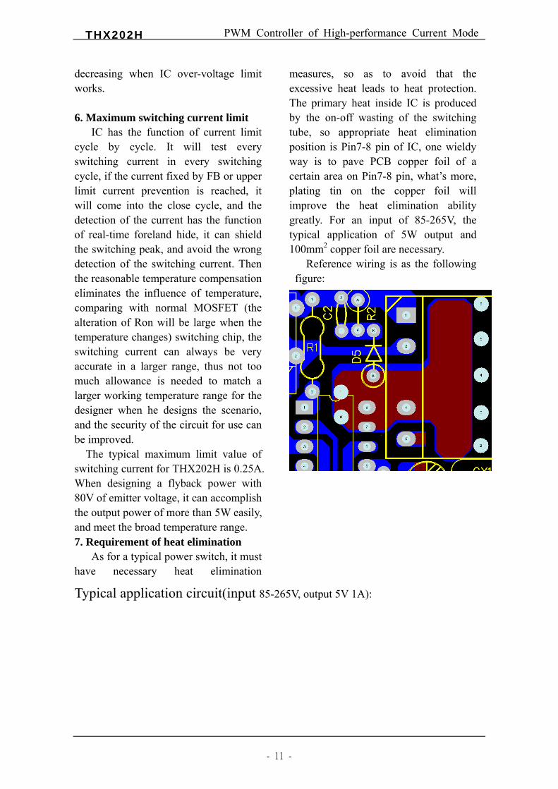
decreasing when IC over-voltage limit works. 6. Maximum switching current limit IC has the function of current limit cycle by cycle. It will test every switching current in every switching cycle, if the current fixed by FB or upper limit current prevention is reached, it will come into the close cycle, and the detection of the current has the function of real-time foreland hide, it can shield the switching peak, and avoid the wrong detection of the switching current. Then the reasonable temperature compensation eliminates the influence of temperature, comparing with normal MOSFET (the alteration of Ron will be large when the temperature changes) switching chip, the switching current can always be very accurate in a larger range, thus not too much allowance is needed to match a larger working temperature range for the designer when he designs the scenario, and the security of the circuit for use can be improved. The typical maximum limit value of switching current for THX202H is 0.25A. When designing a flyback power with 80V of emitter voltage, it can accomplish the output power of more than 5W easily, and meet the broad temperature range. 7. Requirement of heat elimination As for a typical power switch, it must have necessary heat elimination
measures, so as to avoid that the excessive heat leads to heat protection. The primary heat inside IC is produced by the on-off wasting of the switching tube, so appropriate heat elimination position is Pin7-8 pin of IC, one wieldy way is to pave PCB copper foil of a certain area on Pin7-8 pin, what’s more, plating tin on the copper foil will improve the heat elimination ability greatly. For an input of 85-265V, the typical application of 5W output and 100mm2 copper foil are necessary. Reference wiring is as the following figure:
Typical application circuit(input 85-265V, output 5V 1A):
- 11 -

PWM Controller of High-performance Current Mode THX202H
Fig. 4 Typical Application Circuit
Components Listing:
- 12 -

PWM Controller of High-performance Current Mode THX202H
No. Component Name Spec./Model encapsulation Amount Sign
1 Resistance 100R 0805 1 R5 2 1K 0805 1 R6 3 4.7K 1206 2 R1 R9 4 10K,1% 0805 1 R7 5 10.5K,1% 0805 1 R8 6 75K 1206 1 R4 7 1M 1206 2 R2 R3 8 Capacitance 331J/50V 0805 1 C4 9 222/1KV 1206 1 C5 10 223/50V 0805 1 C3 11 681J/50V 0805 1 C7 12 104/50V 0805 1 C8 13 Capacitance Y 222M/400V CT7,Y1 1 CY1 14 ELCC 6.8uF/400V EC3.5-8 2 C1 C2 15 22uF/16V EC3-5 1 C6 16 220uF/16V EC3-6.3 1 C9 17 470uF/16V EC3.5-8 1 C10 18 Diode 1N4001 DO-35 1 D3 19 FR107 DO-41 1 D2 20 SR260 DO-41 1 D4
21 Rectification bridge
DF06S DF-S 1 D1
22 Luminous tube LED2.5 D2.5 1 D5
23 Induction ofcolor code
EC-332K D4*8mm 1 L1
24 Power inductance
DR6*8,10uH DR6*8 1 L2
25 Transformer EE16 EE16-P10 1 T1 26 Insurance tube F1A/250V D4*10mm 1 RF1
27 voltage-dependent resistance
7D471K CT7 1 TZ1
28 IC THX202H DIP8 1 IC1 29 TL431 TO92 1 IC3 30 PC817B DIP4 1 IC2
- 13 -

PWM Controller of High-performance Current Mode THX202H
31 Circuitry panel PCB,28x53mm 1
Coils of the Transformer: 1. Parameters of magnetic core Core : EF16,TDK PC40 Ae=19.8mm2 Aw=39.8mm2
Bobbin : EF16, 10PIN, 4+6PIN,VELOX 420-SEO , 94V0 Lp=3.1mH±10% 2. Bobbin diagram
3. Bobbin data
No. Name Spec. Direction coil/layer Note
1 Np1, 1st segment of maincoil F0.2mm*1P,2UEW 2-1 80TS Thick
coiling
2 insulated adhesive paper 3M,No.1350 -- 3 tiers --
3 Ns, output coil F0.50mm*1P,3UEW 7-8 11TS Thin coiling
4 insulated adhesive paper 3M,No.1350 -- 3 tiers --
5 Np2, 2nd segment ofmain coil F0.2mm*1P,2UEW 3-2 80TS Thick
coiling
6 insulated adhesive paper 3M,No.1350 -- 2 tiers --
7 Nvcc, ICp powersupply coil F0.2mm*1P,2UEW 5-6 13TS Thin
coiling
- 14 -

PWM Controller of High-performance Current Mode THX202H
8 insulated adhesive paper 3M,No.1350 -- 3 tiers --
Note: the transformer is coiled with copper skin 1.1TS and welded to meet Pin6. Testing data:
Input Voltage (V) Unit
85 110 135 180 220 265
Input power (standby power) whenIo=0A W 0.06 0.07 0.08 0.11 0.14 0.21
Output voltage when Io=0A V 5.13 5.12 5.13 5.13 5.13 5.13
Output ripple when Io=0A mV 15.4 13.0 12.8 15.4 16.8 16.4
Output voltage when Io=1A V 5.13 5.12 5.12 5.12 5.12 5.12
Output ripple when Io=1A mV 15.6 14.0 13.4 13.0 13.4 13.4
Switch power when Io=1A % 70.5 73.1 73.9 75.2 73.7 73.1
Output voltage when Io=0.75A V 5.12 5.13 5.12 5.12 5.12 5.12
Output ripple when Io=0.75A mV 11.8 10.2 11.0 11.0 10.2 10.8
Switch efficiency when Io=0.75A % 71.2 76.0 73.9 74.7 73.3 72.7
Output voltage when Io=0.5A V 5.12 5.12 5.12 5.12 5.12 5.12
Output ripple when Io=0.5A mV 11.6 10.8 11.8 10.8 11.8 11.6
Switch efficiency when Io=0.5A % 70.5 73.2 74.4 72.9 71.9 70.9
Output voltage when Io=0.25A V 5.12 5.13 5.12 5.12 5.12 5.12
Output ripple when Io=0.25A mV 10.6 10.8 11.0 10.6 12.4 11.4
Switch power when Io=0.25A % 68.5 70.1 70.7 69.6 67.7 65.3
Input power when the outputsuffers from short circuit W 0.44 0.71 0.89 1.28 1.63 1.92
Testing item
Testing data
- 15 -

PWM Controller of High-performance Current Mode THX202H
Electric load: PROGIGIT 3310D, power meter: GW GPM-8212, Oscillograph: Taike TDS-2014
Primary waveform of testing point: 1. Vce waveform diagram
Vin=85V, Io=0.5A Vin=85V, Io=1A
50V/div 2uS/div50V/div 2uS/div
Vin=110V, Io=0.5A Vin=110V, Io=1A
50V/div 2uS/div 50V/div 2uS/div
Vin=220V, Io=0.5A Vin=220V, Io=1A
100V/div 2uS/div 100V/div 2uS/div
- 16 -

PWM Controller of High-performance Current Mode THX202H
Vin=265V, Io=0.5A Vin=265V, Io=1A
100V/div 5uS/div 100V/div 5uS/div
2. Output noise waveform
Vin=85V, Io=1A Vin=265V, Io=1A
50mV/div 10mS/div 20mV/div 10mS/div
3. Output ripple waveform
Vin=85V, Io=1A Vin=265V, Io=1A
20mV/div 10uS/div 20mV/div 10uS/div
- 17 -

PWM Controller of High-performance Current Mode THX202H
4. Output waveform on start-up
Vin=85V, Io=1A Vin=265V, Io=1A
2.0V/div 10mS/div 2.0V/div 10mS/div
5. Vce and Vo waveform on start-up
Vin=85V, Io=1A Vin=265V, Io=1A
100V/div 200mS/div 5V/div
200V/div 200mS/div 5V/div
6. Vce waveform when the output suffers short circuit
Vin=85V, Io=Short Vin=265V, Io=Short
- 18 -

PWM Controller of High-performance Current Mode THX202H
50V/div 200mS/div 100V/div 500uS/div
- 19 -

PWM Controller of High-performance Current Mode THX202H
Bland for this page)
IC reference junction temperature and heat resistance Data of DIP8 encapsulation junction temperature (reference) (θJC)1…………...………...................................…20 /W (θJA)2…………...………...................................…70 /W
Note:1. the testing point is where Pin7,8 approaches the encapsulation cover 2. Pin7, 8 is connected on two ounces of tinning copper, and the area of copper is not less than 200mm2.
Diagram of the dimension of encapsulation (DIP8)
- 20 -

PWM Controller of High-performance Current Mode THX202H
4
- 21 -