Embed Size (px)
Citation preview

Realtek RTD2660 series
RTD2660 series
Flat Panel Display Controller
Preliminary Revision
Version 1.00 Last updated: 2007/6

Realtek RTD2660 series
2
1. FEATURES...................................................................................................................................5
2. CHIP DATA PATH BLOCK DIAGRAM .................................................................................. 14
3. REGISTER DESCRIPTION ..................................................................................................... 15 Common page .................................................................................................................................. 15 Global Event Flag............................................................................................................................. 15 Watch Dog........................................................................................................................................ 19 Input Video Capture.......................................................................................................................... 21 Input Frame Window........................................................................................................................ 25 FIFO Frequency ............................................................................................................................... 28 Input pattern generator...................................................................................................................... 29 Display Format................................................................................................................................. 30 Display Fine Tune ............................................................................................................................ 35 Cyclic-Redundant-Check.................................................................................................................. 36 FIFO Window................................................................................................................................... 37 Scaling Up Function ......................................................................................................................... 38 Frame Sync Fine Tune ...................................................................................................................... 42 Sync Processor ................................................................................................................................. 43 Macro Vision.................................................................................................................................... 54 Highlight window............................................................................................................................. 55 Color Processor Control.................................................................................................................... 60 Contrast/Brightness Coefficient ........................................................................................................ 61 Gamma Control ................................................................................................................................ 62 Dithering Control ............................................................................................................................. 64 Overlay/Color Palette/Background Color Control ............................................................................. 64 Image Auto Function ........................................................................................................................ 65 Embedded Timing Controller............................................................................................................ 71 TCON Horizontal/Vertical Timing Setting ........................................................................................ 72 Dot Masking..................................................................................................................................... 75 Control for LVDS ............................................................................................................................. 78 Embedded OSD................................................................................................................................ 81 Digital Filter ..................................................................................................................................... 82 VBI .................................................................................................................................................. 84 Video Color Space Conversion ......................................................................................................... 97 Paged Control Register ..................................................................................................................... 98 Embedded ADC (Page 0).................................................................................................................. 99
Embedded VADC..............................................................................................................................................................99 Embedded YPP ADC ......................................................................................................................................................105
ABL(Page 0) .................................................................................................................................. 115 LVR(Page 0)................................................................................................................................... 119 ADC PLL (Page 1) ......................................................................................................................... 120 DISPLAY PLL (Page 1).................................................................................................................. 131 DCLK Spread Spectrum (Page 1) ................................................................................................... 132 MULTIPLY PLL (Page 1) ............................................................................................................ 136 PLL27X ......................................................................................................................................... 137 Reserved Page3~page5 ................................................................................................................... 139 De-interlace(Page 6) ....................................................................................................................... 139 Noise Estimation(Page 6) ............................................................................................................... 141 Peaking and Coring and EMF/ Chroma Lowpass(Page 6) ............................................................... 144

Realtek RTD2660 series
3
YUV422 to YUV444 Conversion & 2to1 Setup(page 6) ................................................................. 147 DCTi (Dynamic Chromance Transition Improvement) in I-Domain(Page 6) ................................... 148 Image Processor Performance (Noise Reduction in I-domain) Register Control(Page 6) ................. 149
Clean PictureTM (Noise Reduction in I-domain) Overall Control ...................................................................................149 Spatial noise reduction (Zoran Filter) .............................................................................................................................149 Impulse noise reduction (Impulse Filter) ........................................................................................................................150
Scale Down(page 6)........................................................................................................................ 150 Linear and Non-linear Scale Down.................................................................................................................................150 UZD_CRC_CTRL..........................................................................................................................................................155
Vivid color-DLTi/DCTi(Page 7)...................................................................................................... 156 Peaking and Coring and EMF/ Chroma Lowpass(page 7) ............................................................... 157 Vivid color-Video Color Space Conversion(page 7)........................................................................ 168 Vivid color-DCC (Page 7)............................................................................................................... 168 Y-Peaking filter and coring control (For Display Domain) .............................................................. 179 Hue/Saturation Control (Page 7) ..................................................................................................... 181 Contrast/Brightness Control (Page 7).............................................................................................. 181 Page 8 Video decoder ..................................................................................................................... 182
Video Control Register ...................................................................................................................................................182 Switch Control Registers ................................................................................................................................................182 Luma Adjustment Registers............................................................................................................................................184 Chroma Adjustment Registers ........................................................................................................................................184 DC Balance Control........................................................................................................................................................185 IRQ Registers..................................................................................................................................................................186 Status Registers_1...........................................................................................................................................................188 Status Registers_2...........................................................................................................................................................189 Reset Register .................................................................................................................................................................191 Auto Mode State Machine Registers. .............................................................................................................................192 Comb Filter Configuration Register ...............................................................................................................................195 Comb Filter Threshold Registers ....................................................................................................................................195 2D YC Separation Registers ...........................................................................................................................................196
Page 9 Video Decoder .................................................................................................................... 203 Clamping/AGC Control Registers ..................................................................................................................................203 Chroma Loop Control Registers .....................................................................................................................................207 HPLL Control Registers .................................................................................................................................................209 Horizontal Sync Detection Registers ..............................................................................................................................212 Vertical Sync and Field Detection Registers ...................................................................................................................214 VSYNC PLL Registers ...................................................................................................................................................216 Chroma DTO Registers...................................................................................................................................................217 Horizontal Sync DTO Registers .....................................................................................................................................217 Auto Mode State Machine Table Status Registers ..........................................................................................................219 Auto Mode Flag Counter Registers ................................................................................................................................220 Auto Mode Flag Adjustment Registers ...........................................................................................................................222 FIFO Control Register ....................................................................................................................................................224 SECAM Control Registers..............................................................................................................................................227 MISC Control Registers..................................................................................................................................................228 Macrovision Control Registers .......................................................................................................................................230 Debug Test ......................................................................................................................................................................231 ADC Clamping Test Mode .............................................................................................................................................234 Chip Version ...................................................................................................................................................................235
Off line sync processor(page B)...................................................................................................... 235 Auto SOY(page B) ......................................................................................................................... 246 Reserved page ................................................................................................................................ 276 MCU register 1(page D) ................................................................................................................. 276
Interrupt Control .............................................................................................................................................................283 ADC................................................................................................................................................................................284 DDC................................................................................................................................................................................289 DDC-CI ..........................................................................................................................................................................293

Realtek RTD2660 series
4
PWM...............................................................................................................................................................................300 I2C Control Module........................................................................................................................................................306
MCU register 2(page E).................................................................................................................. 311 SPI-FLASH.....................................................................................................................................................................311 IrDA................................................................................................................................................................................318 Pin Share.........................................................................................................................................................................326 CEC function ..................................................................................................................................................................335 GPIO Control..................................................................................................................................................................340 SFR Access .....................................................................................................................................................................348 Watchdog Timer..............................................................................................................................................................348 In System Programming .................................................................................................................................................350 Scalar Interface ...............................................................................................................................................................352 Bank Switch....................................................................................................................................................................355
Embedded OSD.............................................................................................................................. 358 OSD Compression.......................................................................................................................... 387 OSD Special Function .................................................................................................................... 388
4. ELECTRIC SPECIFICATION................................................................................................ 399 DC Characteristics.......................................................................................................................... 399
5. MECHANICAL SPECIFICATION......................................................................................... 400
6. ORDERING INFORMATION................................................................................................. 401

Realtek RTD2660 series
5
1. Features General l Embedded 3 DDC with DDC1/2B/CI l Zoom scaling up and down l Embedded one MCU with SPI flash controller. l It contains 8 ADCs in D-connector,LED
backlight,and key pad application l It supports infrared remote function l Require only one crystal to generate all timing. l Programmable internal low-voltage-reset (LVR) l High resolution 6 channels PWM output, and
wide range selectable PWM frequency. l Support input format up to
1920(WUXGA)/1440-pixel width(option) Analog RGB Input Interface l 2 Analog input supported with internal switch l Integrated 8-bit triple-channel 210/165MHz
ADC/PLL(option) l Embedded programmable Schmitt trigger of
HSYNC l Support Sync-On-Green (SOG) and various
kinds of composite sync modes l On-chip high-performance hybrid PLLs l High resolution true 64 phase ADC PLL l Y/Pb/Pr support up to HDTV 1080p resolution Embedded Video Decoder l High performance AV 2D Comb-filter l Support Composite, S Video, Component input l Support VBI with Closed caption/ V chip slicer Video Input Interface l Support 8-bit video (ITU 656) format input Embedded MCU l Industrial standard 8051 core with serial flash up
to 256K bytes l Low speed ADC for various application l Infrared function supported l I2C Master or Slave hardware supported
Auto Detection /Auto Calibration l Input format detection l Compatibility with standard VESA mode and
support user-defined mode l Smart engine for Phase/Image position/Color
calibration Scaling l Fully programmable zoom ratios l Independent horizontal/vertical scaling l Advanced zoom algorithm provides high image
quality l Sharpness/Smooth filter enhancement l Support non-linear scaling from 4:3 to 16:9 or
16:9 to 4:3 Color Processor l True 10 bits color processing engine l sRGB compliance l Advanced dithering logic for 18-bit panel color
depth enhancement l Dynamic overshoot-smear canceling engine l Brightness and contrast control l Programmable 10-bit gamma support l Peaking/Coring/XVYCC function for video
sharpness l DLTI/DCTI/ Noise reduction for video quality VividColorTM l Independent color management (ICM) l Dynamic contrast control (DCC) Output Interface l Fully programmable display timing generator l Flexible data pair swapping for easier system
design. l Programmable TCON function support l 1 and 2 pixel/clock panel support and up to
170MHz, 1920/1440-pixel width(option) l Multi-output interface (LVDS/ TTL)on single
PCB l Spread-Spectrum DPLL to reduce EMI l Fixed Last Line output for perfect panel
capability
Embedded OSD l Embedded 16.5K SRAM dynamically stores
OSD command and fonts l Support multi-color RAM font, 1, 2 and 4-bit per
pixel l 16 color palette with 24bit true color selection l Maximum 8 window with alpha-blending/
gradient /dynamic fade-in/fade-out, bordering/ shadow/3D window type
l Rotary 90,180,270 degree l Independent row shadowing/bordering l Programmable blinking effects for each character l OSD-made internal pattern generator for factory
mode l Support 12x18~4x18 proportional font l Hardware decompression for OSD font l Special function for closed-caption and CGMS
Power & Technology l 3.3V / 1.8V power supply

Realtek RTD2660 Common page
6
RTD2660
5251504948474645444342414039
3837363534333231302928272625242322212019181716151413121110987654321
ARED4/ARED6 /TXEC-
53 54 55 56 57 58 59 60 61 62 63 64
6566676869707172737475767778798081828384858687888990919293949596979899
100101102
103
104
ARED3/ARED5 / TXE2+
ARED7/AGRN3 /TXE3+ARED6/AGRN2 /TXE3-ARED5/ARED7 /TXEC+
ARED2/ARED4 / TXE2-ARED1/ARED3 /TXE1+ARED0/ARED2 /TXE1-DENA/TXE0+DHS/TXE0-
105
106
107
108
109
110
111
112
113
114
115
116
117
118
119
120
121
122
123
124
125
126
127
128
VAD
C_V
DD
v8_7
/Vin
+0RE
SETB
NC
DDC
SCL2
/GPI
O
XO
DDC
SDA
2/G
PIO
XI
v8_0
/AH
S1VC
LK/A
VS1
v8_6
/Vin
-0v8
_5/V
in+1
v8_4
/Vin
-1v8
_3/V
in+2
V8_
2/Vi
n-2
VCCK
GND
K
v8_1
/Vin
+3 NC
PVCC
ABLU1/GPIO/ABLU7/TXO3+ABLU0/GPIO/ABLU6 / TXO3-AGRN7/GPIO/ABLU5 / TXOC+AGRN6/GPIO/ABLU4/ TXOC-AGRN5/GPIO/ABLU3 /TXO2+AGRN4/GPIO/ABLU2 /TXO2-AGRN3/GPIO/AGRN7 /TXO1+AGRN2/GPIO/AGRN6/TXO1-AGRN1/GPIO/AGRN5 /TXO0+AGRN0/GPIO/AGRN4/TXO0-
AHS0
v8_4
AVS0
v8_7v8_6v8_5
v8_0
v8_3v8_2v8_1
NC
B0+G0-
R0-SOG0
G0+
B0-
ADC_GND/VADC_GND
R0+
VDD
GND
NC
NCNCNC
NC
VDD
NC
v8_6/B1+v8_5/G1-
v8_2/R1-v8_3/SOG1
v8_4/G1+
v8_7/B1-
v8_1/R1+
ADC_VDD
v8_0
/Vin
-3
CEC
DD
CSDA
3/G
PIO
DDC
SCL3
/GPI
OV
CCK
SD2/
SPD
IF2/
TCO
N[8]
/GPI
O/II
CSCL
/PW
M1
SPI_
SCLK
/SDI
O
CEB/
IRQ
B
SI/M
CU_S
CLK
SO/S
CSB
MCK
/TCO
N[7]
/GPI
OSC
K/T
CON
[3]/G
PIO
WS/
TCO
N[6
]/GPI
O
SD3/SPDIF3/TCON[10]/GPIO/PWM0
SD0/
SPD
IF0/
TCON
[4]/G
PIO
SD1/
SPD
IF1/
TCO
N[9]
/GPI
OSD
2/SP
DIF
2/TC
ON[
1]/G
PIO
/IrDA
SD3/
SPD
IF3/
TCO
N[13
]/GPI
O/V
CLK
SD0/
SPD
IF0/
TCO
N[9
]/GPI
OSD
1/SP
DIF
1/TC
ON[
5]/G
PIO
/IRQ
B/IIC
SDA
WS/TCON[7][1]/GPIO/PWM1
SD0/
SPDI
F0/T
CON
[0]/G
PIO/
IrDA
B-AD
C2/II
CSDA
/GPI
OB-
AD
C1/II
CSC
L/G
PIO
BAD
C0/P
WM
1/PW
M5/
GPI
O
ABLU2/SPDIF3/SD3/TCON[10][8]/GPIO/PWM1/PWM5
GPIO/PWM2DVS/GPIO/PWM1DCLK/GPIO/PWM0
GPIO/PWM4/TCON[12][3]GPIO/PWM3/TCON[11][6]
GPIO/PWM5/TCON[0]
PVCCPGND
PVCC
PGN
D
ABLU3/SPDIF2/SD2/TCON[9][11]/GPIO/IICSDAABLU4/SPDIF1/SD1/TCON[7][3]/GPIO/IICSCLABLU5/SD0/SPDIF0/TCON[13][3]/GPIO
A-A
DC0/
AVO
UT/V
CLK
/GPI
OA
-AD
C1/G
PIO
A-A
DC2
/GPI
OA
-AD
C3/G
PIO
A-A
DC4
/GPI
O
DDC
SCL1
/GPI
OD
DCS
DA1/
GPI
O
ABLU6/MCK/TCON[5][9]/GPIOABLU7/SCK/TCON[4][2]/GPIO
NCVCCK
NCNC

Realtek RTD2660 Common page
7
(I/O Legend: A = Analog, I = Input, O = Output, P = Power, G = Ground) Name I/O Pin # Description Note
VDD AP 1 power (3.3 V) NC AI 2 Not connected Ref value:
1K ohm V8_0 AI 3 Input/VIDEO 8-0 V8_1 AI 4 Input/VIDEO 8-1 V8_2 AI 5 Input/VIDEO 8-2 V8_3 AI 6 Input/VIDEO 8-3 V8_4 AI 7 Input/VIDEO 8-4 V8_5 AI 8 Input/VIDEO 8-5 V8_6 AI 9 Input/VIDEO 8-6 V8_7 AI 10 Input/VIDEO 8-7 GND AG 11 ground NC AI 12 Not connected NC AI 13 Not connected NC AI 14 Not connected NC AI 15 Not connected NC AI 16 Not connected NC AI 17 Not connected NC AI 18 Not connected NC AI 19 Not connected VDD AP 20 power (3.3 V) AVS0 I 21 ADC vertical sync input no power 5V
tolerance AHS0 I 22 ADC horizontal sync input
AVS0 and AHS0 could be used to select one of three scan chain. AHS0/AVS0: 2’b00: {i_chain[2:0], mcu_chain[1:0], vbi_chain[2:0]} 2’b01: d_chain 2’b10: vdec_chain Other are reserved
no power 5V tolerance
ADC_VDD AG 23 ADC Power (1.8V) B0- AI 24 Negative BLUE analog input (Pb-) B0+ AI 25 Positive BLUE analog input (Pb+) G0- AI 26 Negative GREEN analog input (Y-) G0+ AI 27 Positive GREEN analog input (Y+) SOG0 AI 28 Sync-On-Green R0- AI 29 Negative RED analog input (Pr-) R0+ AI 30 Positive RED analog input (Pr+) B1-/V8_7 AI 31 Negative BLUE analog input
(Pb-)/VIDEO 8-7
B1+/V8_6 AI 32 Positive BLUE analog input (Pb+)/VIDEO 8-6
G1-/V8_5 AI 33 Negative GREEN analog input (Y-)/VIDEO 8-5
G1+/V8_4 AI 34 Positive GREEN analog input (Y+)/VIDEO 8-4
SOG1/V8_3 AI 35 Sync-On-Green/ VIDEO 3 R1-/V8_2 AI 36 Negative RED analog input
(Pr-)/VIDEO 8-2
R1+/V8_1 AI 37 Positive RED analog input

Realtek RTD2660 Common page
8
(Pr+)/VIDEO 8-1 ADC_GND/VADC_GND AP 38 ADC/VADC GND AHS1/V8_0 I 39 ADC horizontal sync input/VIDEO 8-0 no power 5V
tolerance AVS1/VCLK I 40 ADC horizontal sync input/VIDEO
clock no power 5V tolerance
Vin+0/V8_7 AI 41 Positive video analog input 0/VIDEO 8-7
Vin-0/V8_6 AI 42 Negative video analog input 0/VIDEO 8-6
Vin+1/V8_5 AI 43 Positive video analog input 1/VIDEO 8-5
Vin-1/V8_4 AI 44 Negative video analog input 1/VIDEO 8-4
Vin+2/V8_3 AI 45 Positive video analog input 2/VIDEO 8-3
Vin-2/V8_2 AI 46 Negative video analog input 2/VIDEO 8-2
Vin+3/V8_1 AI 47 Positive video analog input 3/VIDEO 8-1
Vin-3/V8_0 AI 48 Negative video analog input 3/VIDEO 8-0
VADC_VDD AG 49 Video decoder ADC POWER (3.3V) A-ADC0/GPIO/AVOUT/VCLK
IO 50 MCU ADC Input /MCU GPIO/AVOUT/VIDEO clock
A-ADC1/GPIO IO 51 6-bit MCU ADC Input/MCU GPIO 6 bit A-ADC2/GPIO IO 52 6-bit MCU ADC Input /MCU GPIO 6 bit A-ADC3/GPIO IO 53 6-bit MCU ADC Input/MCU GPIO 6 bit A-ADC4/GPIO IO 54 6-bit MCU ADC Input /MCU GPIO 6 bit B-ADC0/GPIO/PWM1/PWM5
IO 55
10-bit MCU ADC Input/MCU GPIO/PWM
10 bit
B-ADC1/GPIO/IICSCL IO 56
10-bit MCU ADC Input /MCU GPIOD/IIC BUS
10 bit
B-ADC2/GPIO/IICSDA IO 57
10-bit MCU ADC Input/MCU GPIO/IIC BUS
10 bit
DDCSCL1/GPIO IO 58
DDC1(pen drain I/O)/MCU GPIO No power 5V tolerance
DDCSDA1/GPIO IO 59
DDC1(Open drain I/O)/MCU GPIO No power 5V tolerance
VCCK P 60 Digital Power (1.8V) GNDK G 61 Digital Ground PVCC P 62 Pad power 3.3V NC -- 63 Not connected SD0/SPDIF0/TCON[0]/GPIO/IrDA
IO 64
IIS-SD0 /SPDIF0 / TCON /MCU GPIO/ Infrared remote data pin
WS/GPIO/TCON[7][1]/PWM1
IO 65
IIS-WS /MCU GPIO / TCON /PWM
SCK/TCON[4][2]/GPIO/BLU7
IO 66
IIS-SCK / TCON /MCU GPIO/TTL Data Bus
MCK/TCON[5][9]/GPIO/BLU6
IO 67
IIS-MCK / TCON /MCU GPIO/TTL Data Bus
SD0/SPDIF0/TCON[13][3]/GPIO/BLU5
IO 68
IIS-SD0 /SPDIF0 / TCON /MCU GPIO/TTL Data Bus
SPDIF1/SD1/TCON[7][3]/GPIO/IICSCL/BLU4
IO 69
SPDIF1 /IIS-SD1 / TCON /MCU GPIO/IIC BUS /TTL Data Bus
SPDIF2/SD2/TCON[9][1 IO 70 SPDIF2 /IIS-SD2 / TCON /MCU

Realtek RTD2660 Common page
9
1]/GPIO/IICSDA/BLU3 GPIO/IIC bus/TTL Data Bus SPDIF3/SD3/TCON[10][8]/GPIO/PWM1/PWM5/BLU2
IO
71
SPDIF3 /IIS-SD3 / TCON /MCU GPIO/PWM /TTL Bata Bus
NC -- 72 Not connected VCCK P 73 Digital Power (1.8V) BLU7/BLU1/TXO3+ /GPIO
IO 74
TTL Data Bus(BLU7,BLU1)/LVDS /MCU GPIO
BLU6/BLU0/TXO3- /GPIO
IO 75
TTL Data Bus(BLU6,BLU0)/LVDS /MCU GPIO
BLU5/GRN7/TXOC+ /GPIO
IO 76
TTL Data Bus(BLU5,BLU7)/LVDS/MCU GPIO
BLU4/GRN6/TXOC- /GPIO
IO 77
TTL Data Bus(BLU4,BLU6)/LVDS/MCU GPIO
BLU3/GRN5/TXO2+ /GPIO
IO 78
TTL Data Bus(BLU3,BLU5)/LVDS/MCU GPIO
BLU2/GRN4/TXO2- /GPIO
IO 79
TTL Data Bus(BLU2,BLU4)/LVDS/MCU GPIO
GRN7/GRN3/TXO1+ /GPIO
IO 80
TTL Data Bus(GRN7,GRN3)/LVDS/MCU GPIO
GRN6/GRN2/TXO1- /GPIO
IO 81
TTL Data Bus(GRN6,GRN2)/LVDS/MCU GPIO
GRN5/GRN1/TXO0+ /GPIO
IO 82
TTL Data Bus(GRN5,GRN1)/LVDS/MCU GPIO
GRN4/GRN0/TXO0- /GPIO
IO 83
TTL Data Bus(GRN4,GRN0)/LVDS/MCU GPIO
PVCC P 84 Pad power 3.3V PGND G 85 Pad ground GRN3/RED7/TXE3+ O 86 TTL Data Bus(GRN3,RED7)/LVDS GRN2/RED6/TXE3- O 87 TTL Data Bus(GRN2,RED6)/LVDS RED7/RED5/TXEC+ O 88 TTL Data Bus(RED7,RED5)/LVDS RED6/RED4/TXEC- O 89 TTL Data Bus(RED6,RED4)/LVDS RED5/RED3/TXE2+ O 90 TTL Data Bus(RED5,RED3)/LVDS RED4/RED2/TXE2- O 91 TTL Data Bus(RED4,RED2)/LVDS RED3/RED1/TXE1+ O 92 TTL Data Bus(RED3,RED1)/LVDS RED2/RED0/TXE1- O 93 TTL Data Bus(RED2,RED0)/LVDS TXE0+/DENA O 94 LVDS/TTL Data enable TXE0-/DHS O 95 LVDS/TTL Display H-sync GPIO/PWM0/DCLK IO
96 MCU GPIO/PWM/TTL Display clock No power 5V
tolerance GPIO/PWM1/DVS IO
97 MCU GPIO/PWM/TTL Display V-sync No power 5V
tolerance GPIO/PWM2 IO
98 MCU GPIO/PWM No power 5V
tolerance GPIO/PWM3/TCON[11][6]
IO 99
MCU GPIO/PWM/TCON No power 5V tolerance
GPIO/PWM4/TCON[12][3]
IO 100
MCU GPIO/PWM/TCON No power 5V tolerance
GPIO/PWM5/TCON[0] IO 101
MCU GPIO/PWM/TCON No power 5V tolerance
SD3/SPDIF3/TCON[10]/GPIO/PWM0
IO 102
IIS-SD3/SPDIF3/TCON/MCU GPIO/ PWM
No power 5V tolerance
SD2/SPDIF2/TCON[8]/GPIO/IICSCL/PWM1
IO 103
IIS-SD2/SPDIF2/TCON[8]/MCU GPIO/IICSCL/PWM1
No power 5V tolerance
SD1/SPDIF1/TCON[5]/G IO 104 IIS-SD1/SPDIF1/TCON[5]/MCU No power 5V

Realtek RTD2660 Common page
10
PIO/IRQB/IICSDA GPIO/IRQ Bar/IICSDA tolerance SD0/SPDIF0/TCON[9]/GPIO
IO 105
IIS-SD0/SPDIF0/TCON/MCU GPIO No power 5V tolerance
PVCC P 106 Pad 3.3V power 3.3V PGND P 107 Pad 3.3V GND MCK/TCON[7]/GPIO IO
108 IIS-MCK/TCON/MCU GPIO No power 5V
tolerance SCK/TCON[3]/GPIO IO
109 IIS-SCK/TCON/MCU GPIO No power 5V
tolerance WS/TCON[6]/GPIO IO
110 IIS-WS/TCON/MCU GPIO No power 5V
tolerance SD0/SPDIF0/TCON[4]/GPIO
IO 111
IIS-SD0/SPDIF0/TCON/MCU GPIO No power 5V tolerance
SD1/SPDIF1/TCON[9]/GPIO
IO 112
IIS-SD1/SPDIF1/TCON/MCU GPIO No power 5V tolerance
SD2/SPDIF2/TCON[1]/GPIO/IrDA
IO 113
IIS-SD2/SPDIF2/TCON/MCU GPIO/Infrared remote data pin
No power 5V tolerance
SD3/SPDIF3/TCON[13]/GPIO/VCLK
IO 114
IIS-SD3/SPDIF3/TCON/MCU GPIO/VIDEO 8-clock
No power 5V tolerance
SPI_SCLK/SDIO IO 115
SPI flash serial data input/external MCU serial control I/F data in
No power 5V tolerance
SI/MCU_SCLK IO 116
SPI flash serial clock/external MCU serial control I/F clock
No power 5V tolerance
SO/SCSB IO 117
SPI flash serial data output /external MCU serial control I/F chip select
No power 5V tolerance
CEB/IRQB IO
118
SPI flash chip enable bar/IRQ Bar Note:It should be pulled down to 0 v or pulled up to 3.3 v in order to designate the MCU type(Internal MCU(0 volts) or External MCU(3.3 volts)).
No power 5V tolerance
NC -- 119 Not connected VCCK P 120 Digital 1.8V Power 1.8V DDCSCL3/GPIO IO
121
DDC3(Open drain I/O)/MCU GPIO No power 5V
tolerance DDCSDA3/GPIO IO
122
DDC3(Open drain I/O)/MCU GPIO No power 5V
tolerance DDCSDA2/GPIO IO
123
DDC2(Open drain I/O)/MCU GPIO No power 5V
tolerance DDCSCL2/GPIO IO
124
DDC2(Open drain I/O)/MCUGPIO No power 5V
tolerance RESETB I
125
Chip Reset Bar Low active; No power 5V tolerance
CEC I/O
126
CEC bus Pull up 27k ohm resistance to 3.3V power; No power 5V tolerance
XO AO 127
Crystal Output No power 5V tolerance
XI AI 128 Crystal Input No power 5V
Realtek RTD2660 Common page
11
tolerance
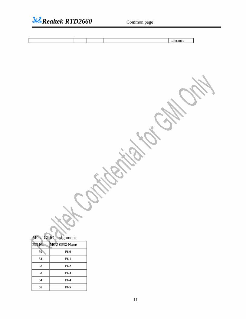
MCU GPIO assignment PIN No. MCU GPIO Name
50 P6.0
51 P6.1
52 P6.2
53 P6.3
54 P6.4
55 P6.5

Realtek RTD2660 Common page
12
56 P6.6
57 P6.7
58 P3.0/RXD(I/O)
59 P3.1/TXD(O)
64 P1.0/T2(I)
65 P1.1/T2EX(I)
66 P1.2/CLKO2(O)
67 P1.3
68 P1.4
69 P1.5
70 P1.6
71 P1.7
74 P9.0
75 P9.1
76 P9.2
77 P9.3
78 P9.4
79 PA.0
80 PA.1
81 PA.2
82 PA.3
83 PA.4
94 P5.0 (removed)
95 P5.1 (removed)
96 P5.2
97 P5.3
98 P5.4
99 P5.5
100 P5.6
101 P5.7
102 P7.6
103 P7.5
104 P7.4
105 P8.0
108 P8.1/CLKO1(O)
Realtek RTD2660 Common page
13
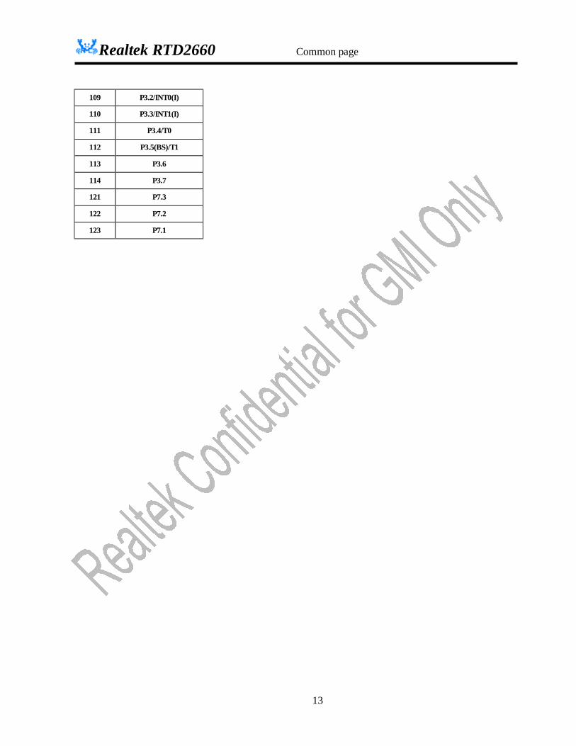
109 P3.2/INT0(I)
110 P3.3/INT1(I)
111 P3.4/T0
112 P3.5(BS)/T1
113 P3.6
114 P3.7
121 P7.3
122 P7.2
123 P7.1

Realtek RTD2660 Common page
14
2. Chip Data Path Block Diagram
Figure 1

Realtek RTD2660 Common page
15
3. Register Description Common page Global Event Flag Register::ID_Reg 0x00
Name Bit R/W Default Description Config
ID 7:0 R 0xf1 MSB 4 bits: 1111 product code
LSB 4 bits: 0001rev. code
Register:: Host_ctrl 0x01
Name Bit R/W Default Description Config.
Rev 7 --- 0 Reserved
Reset_chk 6 R/W 0 Reset Check Once scalar is reset, this value will be cleared to 0.The purpose of it is to check if LVR has been triggered. It should be written to 1 ahead, then read it..LVR has been triggered if the value is 0,else LVR has not.
Rev 5:3 --- --- Reserved
PD_EN 2 R/W 0 Power Down Mode Enable
0: Normal (Default)
1: Enable power down mode
Turn off ADC RGB Channel/ ADC
Band-gap/ SOG/ DPLL/ LVDS/ADC
PLL/ SYNC- PROC/ AUTO SOY
ADC/VADC/m2pll
PS_EN 1 R/W 1 Power Saving Mode Enable
0: Normal
1: Enable power saving mode (Default)
Turn off ADC RGB channel/ DPLL/
LVDS/ ADC PLL/VADC / m2pll
When power down or power saving
function is enabled, internal mcu clock
is forced to crystal clock.
Sft_Reset 0 R/W 0 Software Reset Whole Chip (Low
pulse at least 8ms)
0: Normal (Default)
1: Reset
Realtek RTD2660 Common page
16
All registers are reset to default except
HOST_CTRL and power-on-latch.
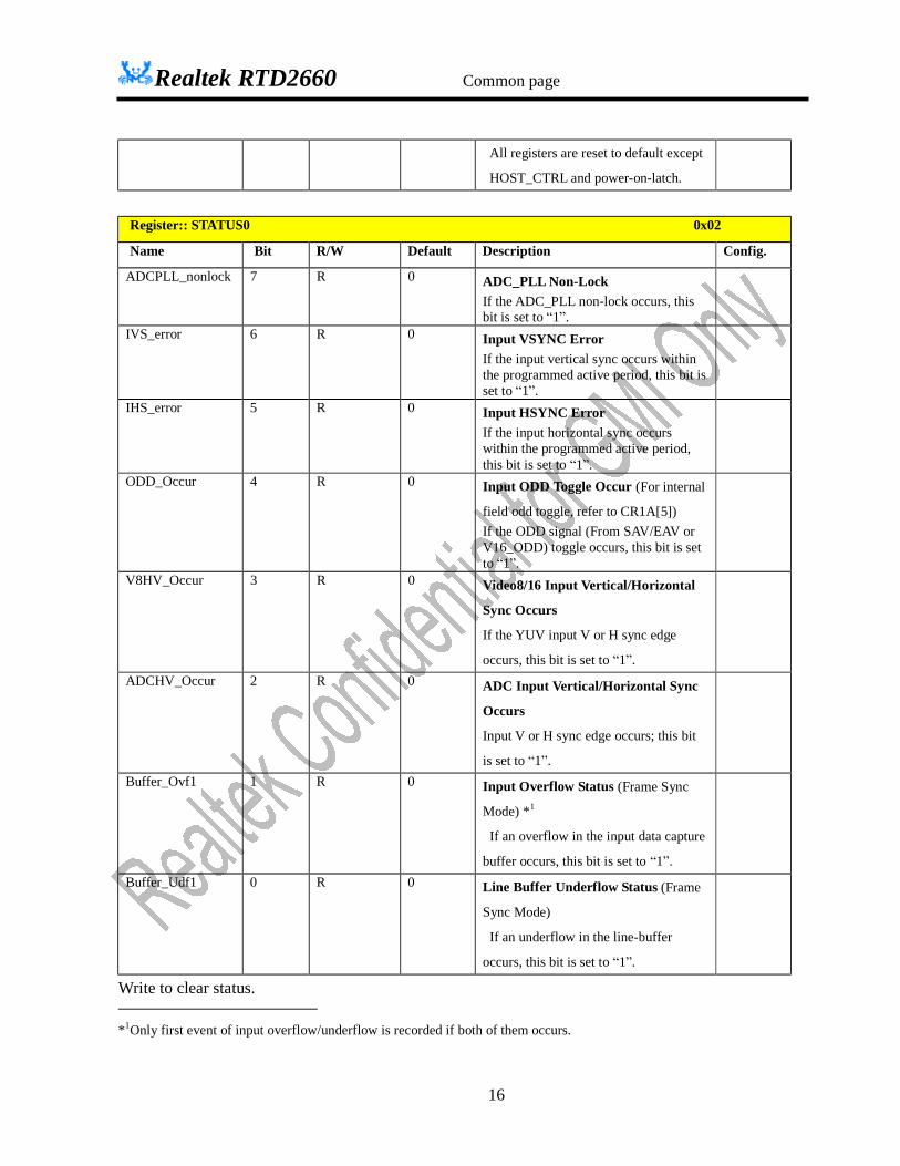
Register:: STATUS0 0x02
Name Bit R/W Default Description Config.
ADCPLL_nonlock 7 R 0 ADC_PLL Non-Lock If the ADC_PLL non-lock occurs, this bit is set to “1”.
IVS_error 6 R 0 Input VSYNC Error If the input vertical sync occurs within the programmed active period, this bit is set to “1”.
IHS_error 5 R 0 Input HSYNC Error If the input horizontal sync occurs within the programmed active period, this bit is set to “1”.
ODD_Occur 4 R 0 Input ODD Toggle Occur (For internal
field odd toggle, refer to CR1A[5]) If the ODD signal (From SAV/EAV or V16_ODD) toggle occurs, this bit is set to “1”.
V8HV_Occur 3 R 0 Video8/16 Input Vertical/Horizontal
Sync Occurs
If the YUV input V or H sync edge
occurs, this bit is set to “1”.
ADCHV_Occur 2 R 0 ADC Input Vertical/Horizontal Sync
Occurs
Input V or H sync edge occurs; this bit
is set to “1”.
Buffer_Ovf1 1 R 0 Input Overflow Status (Frame Sync
Mode) *1
If an overflow in the input data capture
buffer occurs, this bit is set to “1”.
Buffer_Udf1 0 R 0 Line Buffer Underflow Status (Frame
Sync Mode)
If an underflow in the line-buffer
occurs, this bit is set to “1”.
Write to clear status. *1Only first event of input overflow/underflow is recorded if both of them occurs.

Realtek RTD2660 Common page
17
Register:: STATUS1 0x03
Name Bit R/W Default Description Config.
Buffer_Ovf2 7 R 0 Line Buffer Overflow Status 1: Line Buffer overflow has occurred since the last status cleared
Buffer_Udf2 6 R 0 Line Buffer Underflow Status 1: Line Buffer underflow has occurred since the last status cleared
DENA_Stop 5 R 0 DENA Stop Event Status 1: If the DENA stop event occurred since the last status cleared
DENA_Start 4 R 0 DENA Start Event Status 1: If the DENA start event occurred since the last status cleared as an interrupt source
DVS_Start 3 R 0 DVS Start Event Status
1: If the DVS start event occurred
since the last status cleared
IENA_Stop 2 R 0 IENA Stop Event Status
1: If the IENA stop event occurred
since the last status cleared
IENA_Start 1 R 0 IENA Start Event Status
1: If the IENA start event occurred
since the last status cleared
IVS_Start 0 R 0 IVS Start Event Status 1: If the IVS start event occurred since the last status cleared
Write to clear status. Register::IRQ_CTRL0 0x04
Name Bit R/W Default Description Config.
IRQ_EN 7 R/W 0 Internal IRQ Enable: (Global)
0: Disable these interrupt. 1: Enable these interrupt.
IRQ_ADCPLL 6 R/W 0 IRQ (ADC_PLL Non-Lock)
0: Disable the ADC_PLL non-lock
error event as an interrupt source 1: Enable the ADC_PLL non-lock error event as an interrupt source
IRQ_IHV 5 R/W 0 IRQ (Input VSYNC/HSYNC Error)
(DEN across Vsync or Hsync)
0: Disable the Input VSYNC/HSYNC

Realtek RTD2660 Common page
18
error event as an interrupt source 1: Enable the Input VSYNC/HSYNC error event as an interrupt source
IRQ_ODD 4 R/W 0 IRQ (Input ODD Toggle Occur)
(EAV/SAV from Video8/16 or
V16_ODD)
0: Disable Input ODD toggle event as
an interrupt source 1: Enable the Input ODD toggle event as an interrupt source
IRQ_V8_HV 3 R/W 0 IRQ (Video8/16 Input Hsync/Vertical
Sync Occurs)
0: Disable the Video8/16 Input Hsync
or Vsync event as an interrupt source 1: Enable the Video8/16 Input Hsync or Vsync event as an interrupt sourc
IRQ_ADC_HV 2 R/W 0 IRQ (ADC Input Hsync/Vertical Sync
Occurs)
0: Disable the ADC Input Hsync or
Vsync event as an interrupt source 1: Enable the ADC Input Hsync or Vsync event as an interrupt source
IRQ_Buffer 1 R/W 0 IRQ (Line Buffer
Underflow/Overflow Status)
0: Disable the Line Buffer
underflow/overflow event as an
interrupt source 1: Enable the Line Buffer underflow/overflow event as an interrupt source
IRQ_IENA 0 R/W 0 IRQ (Input ENA Start Event
Occurred Status)
0: Disable IENA start as interrupt
source 1: Enable IENA start as interrupt source
Register:: New_added_status0 0x07
Name Bit R/W Default Description Config.
Wstate 7 R --- Wait state status

Realtek RTD2660 Common page
19
New_m_state 6 R --- New mode state
Change_m_happen 5 R --- Change mode happen (it will not be triggered while VGIP active signal is low)
Wstate_IRQ_en 4 R/W 0 IRQ enable of Wait state status 0:disable 1:enable
New_m_state_IRQ_en
3 R/W 0 IRQ enable of New mode status 0:disable 1:enable
Change_m_happen_IRQ_en
2 R/W 0 IRQ enable of change mode happen status 0:disable
1:enable
VD_IRQ 1 R --- VD IRQ status VBI_Statua 0 R --- VBI status
Register:: New_added_status1 0x08
Name Bit R/W Default Description Config.
SOY0_status 7 R --- Auto SOY0 one time measure status SOY1_status 6 R --- Auto SOY1 one time measure status Reserved 5:0 --- --- Reserved
Address: 09~0B Reserved Watch Dog Address: 0C WATCH_DOG_CTRL0 Default: 00h
Bit Mode Function
7 R/W Auto Switch When Input HSYNC/VSYNC Error
0: Disable (Default)
1: Enable
(See CR02[6] and CR02[5])
6 R/W Auto Switch When Input HSYNC/VSYNC Timeout or Overflow
0: Disable (Default)
1: Enable
(See CR52[4] and CR54[5:4])
5 R/W Auto Switch When Display VSYNC Timeout
0: Disable (Default)
1: Enable
4 R/W Auto Switch When ADC-PLL Unlock
0: Disable (Default)
1: Enable
3 R/W Auto Switch When Overflow or Underflow (for Frame-Sync Display)
0: Disable (Default)

Realtek RTD2660 Common page
20
1: Enable
2 R/W Watch-Dog Action if Event Happened (for Display Timing)
0: Disable (Default)
1: Free Run
1 R/W Watch-Dog Action if Event Happened (for Display Data)
0: Disable (Default)
1: Background
(Turn off overlay function and switch to background display simultaneously)
0 R Display VSYNC Timeout Flag (for CR0C[5])
0: DVS is present
1: DVS is timeout
The line number of Display HS is equal to Display Vertical Total; this bit is set to “1”. (Write to
clear status).
Address: 0D WATCH_DOG_CTRL1 Default: 00h
Bit Mode Function
7 R/W Auto Switch When Input HSYNC Changed
0: Disable (Default)
1: Enable
(See CR58[3])
6 R/W Auto Switch When Input VSYNC Changed
0: Disable (Default)
1: Enable
(See CR58[2])
5 R/W Wstate WD enable 0:Disable(Default) 1:enable
4 R/W New_m_state
0:Disable(Default)
1:enable
3 R/W Change_mode_happen
0:Disable(Default)
1:enable
2:0 --- Reserved
Address: 0E~0F Reserved

Realtek RTD2660 Common page
21
Input Video Capture Address: 10 VGIP_CTRL (Video Graphic Input Control Register) Default: 00h
Bit Mode Function
7 R/W 8 bit Random Generator
0: Disable(Default)
1: Enable
6 R/W Input Test Mode:
0: Disable (Default)
1: Video8 input will go through RGB channel, AVS=>IVS, AHS=>IHS, VCLK=>ICLK 5 R/W VGIP Double Buffer Ready
0: Not Ready to Apply
1: Ready to Apply
When the list table of CR10[4] is set, then enable CR10[5]. Remember to set CR13[3] to
decide which one condition to use. Finally, hardware will auto load these values into VGIP double buffer registers as the
trigger event happens and clear CR10[5] to 0.
4 R/W VGIP Double Buffer Mode Enable (Each register described below has its own double buffer)
0: Disable (Original- Write instantly by MCU write cycles)
1: Enable (Double Buffer Function Write Mode)
Register Trigger Event
PLLPHASE(CRB3,CRB4) Add 1-clk Delay to IHS Delay (CR12[4]) HSYNC Synchronize Edge (CR12[3])
Falling edge of Ivactive
IPH_ACT_STA (CR14[2:0],CR15) Falling edge of Ivactive
IPV_ACT_STA (CR18[2:0],CR19) IV_DV_LINES (CR40)
Falling edge of Ivactive
IVS_DELAY (for capture) (CR1C,CR1E[1]) Falling edge of Ivactive
IHS_DELAY (for capture) (CR1D, CR1E[0]) Falling edge of Ivactive
IPH_PORCH_NUM (CR1F[2:0],CR20) Falling edge of Ivactive
3:2 R/W Input Pixel Format
00: Embedded ADC (ADC_HS)(Default)
01: Reserved
10: Video8
11: Video Decorder Input(Video 16)
1 R/W Input Graphic/Video Mode
0: From analog input (input captured by ‘Input Capture Window’) (Default)

Realtek RTD2660 Common page
22
1: From digital input (captured start by ‘enable signal’, but sill stored in ‘capture window size’) 0 R/W Input Sampling Run Enable
0: No data is transferred (Default)
1: Sampling input pixels
Address: 11 VGIP_SIGINV (Input Control Signal Inverted Register) Default: 00h
Bit Mode Function
7 R/W Safe Mode
0: Normal (Default)
1: Safe Mode Enable, mask 1 frame IVS of every 2 frame IVS, slow down input frame rate.
6 R/W IVS Sync with IHS Control (Avoid VS bouncing)
0: Enable (Default)
1: Disable
5 R/W HS Signal Inverted for Field Detection
0: Negative Edge (Default)
1: Positive Edge
4 R/W Input Video ODD Signal Invert Enable
0: Not inverted (ODD = positive polarity) (Default)
1: Inverted (ODD = negative polarity)
3 R/W Input VS Signal Polarity Inverted
0: Not inverted (VS = positive polarity) (Default)
1: Inverted (VS = negative polarity)
2 R/W Input HS Signal Polarity Inverted
0: Not inverted (HS = positive polarity) (Default)
1: Inverted (HS = negative polarity)
1 R/W Input ENA Signal Polarity Inverted
0: Not inverted (input high active) (Default)
1: Inverted (while input low active)
0 R/W Video Input Clock Polarity
0: Rising edge latched (Default)
1: Falling edge latched
Address: 12 VGIP_DELAY_CTRL Default: 00h
Bit Mode Function
7 R 6-Iclk-delay HS Level Latched by VS Rising Edge
6 R HS Level Latched by VS Rising Edge
5 R HS Level Latched by 6-Iclk-delay VS Rising Edge
4 R/W/D Add One Clock Delay to IHS Delay
Realtek RTD2660 Common page
23
0: Disable (Default)
1: Enable
3 R/W/D HSYNC Synchronize Edge
0: HSYNC is synchronized by the positive edge of the input clock
1: HSYNC is synchronized by the negative edge of the input clock
( HSYNC source is selected by CR48[0] and then synchronized )
2 R/W VSYNC Synchronize Edge
0: Latch VS by the negative edge of input HSYNC (Default)
1: Latch VS by the positive edge of input HSYNC
1:0 R/W Video Input Clock Delay Control:
00: Normal (Default)
01: 1ns delay
10: 2ns delay
11: 3ns delay
Address: 13 VGIP_ODD_CTRL (Video Graphic Input ODD Control Register) Default: 00h
Bit Mode Function
7 R/W ODD Inversion for ODD-Controlled-IVS-Delay
0: Not Invert (Default)
1: Invert
6 R/W ODD-Controlled-IVS-Delay One-Line Enable
0: Disable (Default)
1: Enable
(Both for Auto and Capture)
5 R/W Safe Mode ODD Inversion
0: Not inverted (Default)
1: Inverted
4 R/W Force ODD Toggle Enable (Without ODD/EVEN Toggle Select in Safe Mode)
0: Disable (Default)
1: Enable
3 R/W VGIP Double Buffer Condition Select Depends on which one signal to decide that VGIP Double Buffer write into registers really. 0: module SDNR v_active end pulse (Default)
1: module VGIPMAIN v_active end pulse
(This bit should be always valid only while VGIP Double Buffer Mode Enable CR10[4] is
enable and VGIP Double Buffer Ready CR10[5] is apply.)

Realtek RTD2660 Common page
24
2 R/W VGIP 1x 2x Clock Sel
0: 1x => Non interlaced source (default)
1: 2x => For interlaced source
1 R/W EAV Error Correction Enable in Video-8/Video-16
0: Disable
1: Enable
0 R/W Internal ODD Signal Selection
0: ODD signal from EAV or YPbPr (Default)
1: Internal Field Detection ODD signal (Also support under VGA input)

Realtek RTD2660 Common page
25
Input Frame Window (All capture window setting unit is 1)
Address: 14 IPH_ACT_STA_H (Input Horizontal Active Start) Default: 00h
Bit Mode Function
7:3 R/W Reserved
2:0 R/W/D Input Video Horizontal Active Start -- High Byte [10:8]
Address: 15 IPH_ACT_STA_L (Input Horizontal Active Start Low) Default: 00h
Bit Mode Function
7:0 R/W/D Input Video Horizontal Active Start -- Low Byte [7:0]
l In analog mode, IPH_ACT_STA means the delay number of pixel clock from the leading edge of HS to the first
pixel of each active line. Actual delay number of pixel clock = IPH_ACT_STA(>=2) +2,
l In digital mode, IPH_ACT_STA means the delay number of pixel clock from the leading edge of DE to the first
pixel of each active line. Actual delay number of pixel clock = IPH_ACT_STA(>=0)
Address: 16 IPH_ACT_WID_H (Input Horizontal Active Width High) Default: 00h
Bit Mode Function
7 R/W Video8 -C-Port Input Latch Bus MSB to LSB Swap Control:
0: Normal (Default)
1: Swap Video8 -C-port MSB to LSB sequence into LSB to MSB
6 R/W ADC Input G/B Swap
0: No Swap
1: Swap
5 R/W ADC Input R/B Swap
0: No Swap
1: Swap
4 R/W ADC Input R/G Swap
0: No Swap
1: Swap
3 R/W Video8 switch
0: Video8(Default)
1: Reserved
2:0 R/W Input Video Horizontal Active Width – High Byte [10:8]
B
G
R R
G
B
CR16[4] CR16[5] CR16[6]
RTD

Realtek RTD2660 Common page
26
Address: 17 IPH_ACT_WID_L (Input Horizontal Active Width Low) Default: 00h
Bit Mode Function
7:0 R/W Input Video Horizontal Active Width -- Low Byte [7:0]
This register defines the number of active pixel clocks to be captured.
Address: 18 IPV_ACT_STA_H (Input Vertical Active Start High) Default: 00h
Bit Mode Function
7:6 R/W Video 8 source sel
00: reserved
01: from ADC
10: from Video decoder
11: reserved 5 R/W Video16 Y/C Port Swap Function
0: Disable Video16 Y/C Port Swap
1: Enable Video16 Y/C Port Swap
4 R/W Video8 / Video16 Select
0: Video8
1: Video16 3 R/W Video16-Y-port Input Latch Bus MSB to LSB Control:
0: Normal (Default)
1: Swap Video16-Y-port MSB to LSB sequence into LSB to MSB
2:0 R/W/D Input Video Vertical Active Start – High Byte [10:8]
Address: 19 IPV_ACT_STA_L (Input Vertical Active Start Low) Default: 00h
Bit Mode Function
7:0 R/W/D Input Video Vertical Active Start – Low Byte [7:0]
The numbers of lines from the leading edge of selected input video VSYNC to the first line of the active window.
The value above should be larger than 1.
Address: 1A IPV_ACT_LEN_H (Input Vertical Active Lines) Default: 00h
Bit Mode Function
7 R SAV/EAV 2-Bit Error Happened (Set if happened and write to clear)
6 R SAV/EAV 1-Bit Error Happened (Set if happened and write to clear)
5 R Internal Field Detection ODD Toggle Happened (Set if happened and write to clear)
The function should be worked under no input clock
4:3 R Number of Input HS between 2 Input VS (LSB bit [1:0])
2:0 R/W Input Video Vertical Active Lines – High Byte [10:8]
Address: 1B IPV_ACT_LEN_L (Input Vertical Active Lines) Default: 00h
Realtek RTD2660 Common page
27
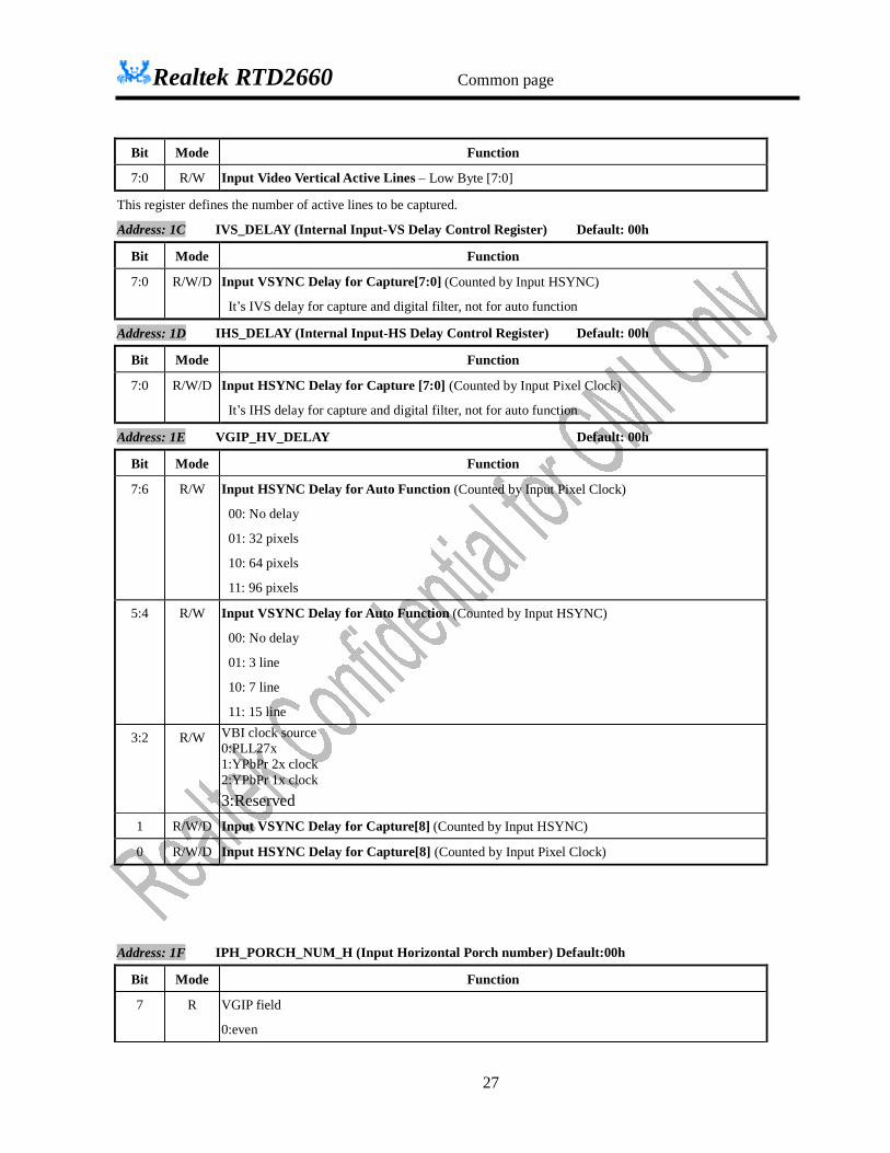
Bit Mode Function
7:0 R/W Input Video Vertical Active Lines – Low Byte [7:0]
This register defines the number of active lines to be captured.
Address: 1C IVS_DELAY (Internal Input-VS Delay Control Register) Default: 00h
Bit Mode Function
7:0 R/W/D Input VSYNC Delay for Capture[7:0] (Counted by Input HSYNC)
It’s IVS delay for capture and digital filter, not for auto function
Address: 1D IHS_DELAY (Internal Input-HS Delay Control Register) Default: 00h
Bit Mode Function
7:0 R/W/D Input HSYNC Delay for Capture [7:0] (Counted by Input Pixel Clock)
It’s IHS delay for capture and digital filter, not for auto function
Address: 1E VGIP_HV_DELAY Default: 00h
Bit Mode Function
7:6 R/W Input HSYNC Delay for Auto Function (Counted by Input Pixel Clock)
00: No delay
01: 32 pixels
10: 64 pixels
11: 96 pixels
5:4 R/W Input VSYNC Delay for Auto Function (Counted by Input HSYNC)
00: No delay
01: 3 line
10: 7 line
11: 15 line
3:2 R/W VBI clock source 0:PLL27x 1:YPbPr 2x clock 2:YPbPr 1x clock 3:Reserved
1 R/W/D Input VSYNC Delay for Capture[8] (Counted by Input HSYNC)
0 R/W/D Input HSYNC Delay for Capture[8] (Counted by Input Pixel Clock)
Address: 1F IPH_PORCH_NUM_H (Input Horizontal Porch number) Default:00h
Bit Mode Function
7 R VGIP field
0:even
Realtek RTD2660 Common page
28
1:odd
6:5 --- Reserved
4 R/W Video decoder vsync select
0:video vsync
1:video v-active_negative
3 R/W I2D_SRC_SEL: IVS to DVS, IHS to DHS Source Select 0: 0: Using SDNR output IVS/IHS/Field as source (Default) 1: Using VGIP hvs_dly output IVS/IHS/Field as source
2:0 R/W/D Input Video Horizontal PORCH NUM -- High Byte [10:8]
Address: 20 IPH_PORCH_NUM_L (Input Horizontal Porch number) Default: 80h
Bit Mode Function
7:0 R/W/D Input Video Horizontal PORCH NUM -- High Byte [7:0]
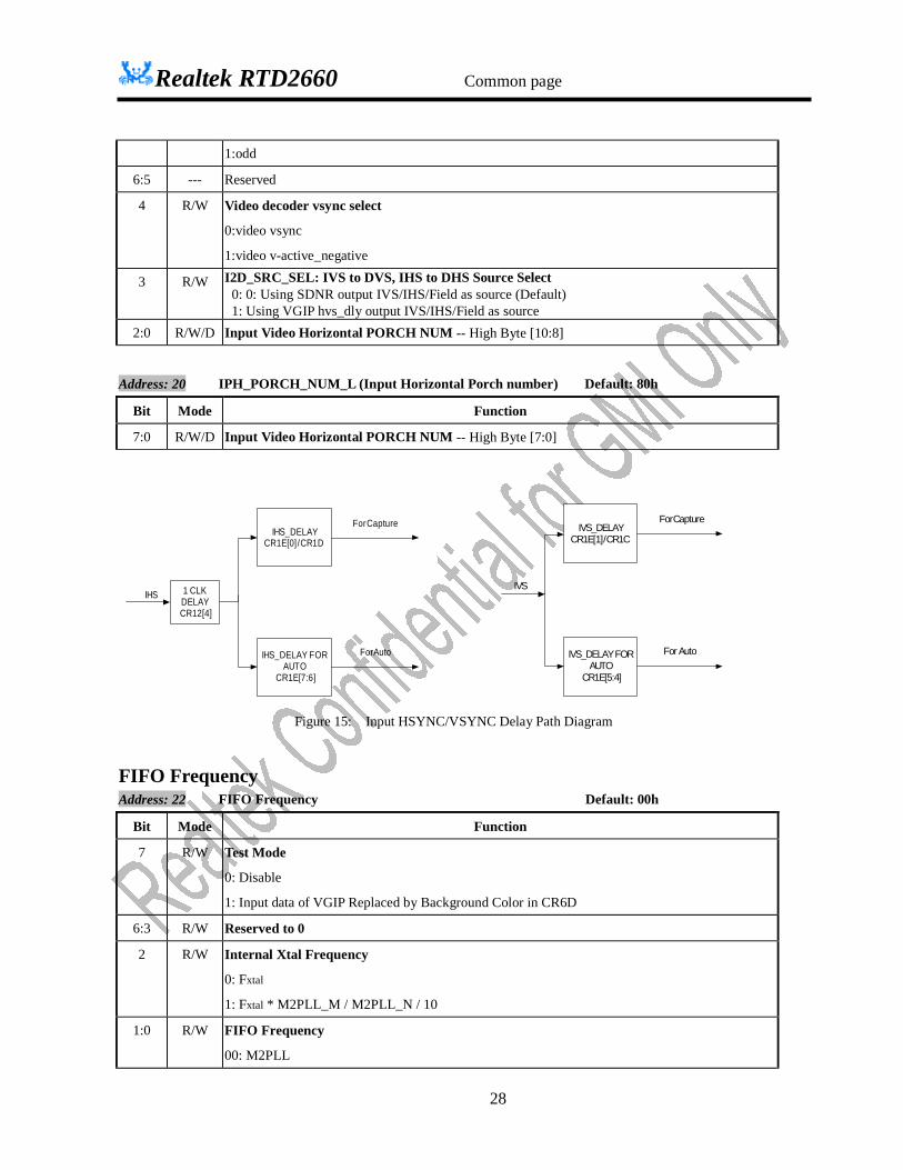
IHS_DELAYCR1E[0] / CR1D
IHS_DELAY FORAUTO
CR1E[7:6]
1 CLKDELAYCR12[4]
For Capture
For Auto
IHS
IVS_DELAYCR1E[1] / CR1C
IVS_DELAY FORAUTO
CR1E[5:4]
For Capture
For Auto
IVS
Figure 15: Input HSYNC/VSYNC Delay Path Diagram
FIFO Frequency Address: 22 FIFO Frequency Default: 00h
Bit Mode Function
7 R/W Test Mode
0: Disable
1: Input data of VGIP Replaced by Background Color in CR6D
6:3 R/W Reserved to 0
2 R/W Internal Xtal Frequency
0: Fxtal
1: Fxtal * M2PLL_M / M2PLL_N / 10
1:0 R/W FIFO Frequency
00: M2PLL

Realtek RTD2660 Common page
29
01: ICLK
10: DCLK
11: Test clock
Input pattern generator Address: 23 FIFO_BIST_CTRL (FIFO BIST Control Register) Default: 00h
Bit Mode Function
7 R Bist for FiFo ok
0: Fail
1: Ok
6 --- Reserved
5 R/W Fifo Bist Function Start (Auto clear to 0 when finish)
0: Finish
1: Start
4:0 --- Reserved
Address: 24 Input Pattern Generator_Access_Port Control Default:00h
Bit Mode Function
7 R/W Enable Input_Pattern_Generator access port by CR25
6:5 -- Reserved to 0
4:0 R/W Input Pattern_Generator port address in CR25
Address: 25-10 Input Pattern Generator Ctrl 0 Default: 8’h00
Bit Mode Function 7 R/W Pattern reset to initial value
0 : 1 frame 1 : 16 frame
6 R/W Random generator mode 0 : x^7 + x^4 + x^3 + x^2 + 1 1 : x^24+x^4+x^3+x^1+1 (Green, Blue, Red )
5 R/W Data update (RED) 0 : reference data enable(pixel base) 1: reference horizontal data enable end(line base)
4 R/W Data update (GREEN) 0 : reference data enable 1: reference horizontal data enable end
3 R/W Data update (BLUE) 0 : reference data enable 1: reference horizontal data enable end
2 R/W Pattern generator mode (RED) 0 : random generator (ref. CR25-10[6] 1 : pattern generator (reg. CR25-11[2])
1 R/W Pattern generator mode (GREEN) 0 : random generator (ref. CR25-10[6] 1 : pattern generator (reg. CR25-11[1])
0 R/W Pattern generator mode (BLUE) 0 : random generator (ref. CR25-10[6]

Realtek RTD2660 Common page
30
1 : pattern generator (reg. CR25-11[0])
Address: 25-11 Input Pattern Generator Ctrl 1 Default: 8’h00
Bit Mode Function 7-3 R/W Reserved to 0 2 R/W Pattern generator (RED)
0 : Out(n) = Out(n-1) 1: Out(n) = Out(n-1) + 1
1 R/W Pattern generator (GREEN) 0 : Out(n) = Out(n-1) 1: Out(n) = Out(n-1) + 1
0 R/W Pattern generator (BLUE) 0 : Out(n) = Out(n-1) 1: Out(n) = Out(n-1) + 1
Address: 25-12 Input Pattern Generator RED Initial Value Default: 8’h01
Bit Mode Function 7-0 R/W RED Initial Value [7:0]
Address: 25-13 Input Pattern Generator GREEN Initial Value Default: 8’h01
Bit Mode Function 7-0 R/W Green Initial Value [7:0]
Address: 25-14 Input Pattern Generator BLUE Initial Value Default: 8’h01
Bit Mode Function 7-0 R/W BLUE Initial Value [7:0]
Address: 26~27 Reserved Display Format Address: 28 VDIS_CTRL (Video Display Control Register) Default: 20h
Bit Mode Function
7 R/W Force Display Timing Generator Enable: (Should be set when in Free-Run mode)
0: wait for input IVS trigger
1: force enable
6 R/W Display Data Output Inverse Enable
0: Disable (Default)
1: Enable (only when data bus clamp to 0)
5 R/W Display Output Force to Background Color
0: Display output operates normally
1: Display output is forced to the color as selected by background color (CR6D) (Default)
4 R/W Display 18 bit RGB Mode Enable
0: All individual output pixels are full 24-bit RGB (Default)
1: All individual output pixels are truncated to 18-bit RGB (LSB 2 bits = 0)
3 R/W Frame Sync Mode Enable
0: Free running mode (Default)
1: Frame sync mode

Realtek RTD2660 Common page
31
2 R/W Display Output Double Port Enable
0: Single port output (Default)
1: Double port output 1 R/W Display Output Run Enable
0: DHS, DVS, DEN & DATA bus are clamped to “0” (Default)
1: Display output normal operation.
0 R/W Display Timing Run Enable
0: Display Timing Generator is halted, Zoom Filter halted (Default)
1: Display Timing Generator and Zoom Filter enabled to run normally
Steps to disable output: First set CR28[1]=0, set CR28[6], then set CR28[0]=0 to disable output.
Address: 29 VDISP_SIGINV (Display Control Signal Inverted) Default: 00h
Bit Mode Function
7 R/W DHS Output Format Select (only available in Frame Sync )
0: The first DHS after DVS is active (Default)
1: The first DHS after DVS is inactive
6 R/W Display Data Port Even/Odd Data Swap:
0: Disable (Default)
1: Enable
5 R/W Display Data Port Red/Blue Data Swap
0: Disable (Default)
1: Enable
4 R/W Display Data Port MSB/LSB Data Swap
0: Disable (Default)
1: Enable
3 R/W Skew Display Data Output
0: Non-skew data output (Default)
1: Skew data output
2 R/W Display Vertical Sync (DVS) Output Invert Enable:
0: Display Vertical Sync output normal active high logic (Default)
1: Display Vertical Sync output inverted logic
1 R/W Display Horizontal Sync (DHS) Output Invert Enable:
0: Display Horizontal Sync output normal active high logic (Default)
1: Display Horizontal Sync output inverted logic
0 R/W Display Data Enable (DEN) Output Invert Enable:
0: Display Data Enable output normal active high logic (Default)
1: Display Data Enable output inverted logic

Realtek RTD2660 Common page
32
Address: 2A DISP_ADDR (Display Format Address Port)
Bit Mode Function
7 R/W Display Setting Double buffer enable
0 : Disable
1 : Enable
Register Trigger Event
DH_TOTAL DVS Rising
ODD_FIXED_LAST
EVEN_FIXED_LAST
DVS Rising
6 R/W Display Double Buffer Ready
0: Not Ready to Apply
1: Ready to Apply
When the list table of DISP_ADDR[7] is set, then enable DISP_ADDR[6], finally, hardware will
auto load these value into RTD as the trigger event happens and clear DISP_ADDR[6] to 0.
5:0 R/W Display Format Address
Address: 2B DISP_DATA (Display Format Data Port)
Bit Mode Function
7:0 R/W Display Format Data
Address: 2B-00 DH_TOTAL_H (Display Horizontal Total Pixels)
Bit Mode Function
7:4 -- Reserved to 0
3:0 R/W Display Horizontal Total Pixel Clocks: High Byte[11:8]
Address: 2B-01 DH_TOTAL_L (Display Horizontal Total Pixels)
Bit Mode Function
7:0 R/W Display Horizontal Total Pixel Clocks: Low Byte[7:0]
Real DH_Total (Target value)= DH_Total (Register value)+ 4
Address: 2B-02 DH_HS_END (Display Horizontal Sync End)
Bit Mode Function
7:0 R/W Display Horizontal Sync End[7:0]:
Determines the width of DHS pulse in DCLK cycles
Address: 2B-03 DH_BKGD_STA_H (Display Horizontal Background Start)
Bit Mode Function
7:4 -- Reserved to 0
3:0 R/W Display Horizontal Background Start: High Byte [11:8]
Address: 2B-04 DH_BKGD_STA_L (Display Horizontal Background Start)

Realtek RTD2660 Common page
33
Bit Mode Function
7:0 R/W Display Horizontal Background Start: Low Byte [7:0]
Determines the number of DCLK cycles from leading edge of DHS to first pixel of Background region.
Real DH_BKGD_STA (Target value)= DH_BKGD_STA (Register value)+ 10
Address: 2B-05 DH_ACT_STA_H (Display Horizontal Active Start)
Bit Mode Function
7:4 -- Reserved to 0
3:0 R/W Display Horizontal Active Region Start: High Byte [11:8]
Address: 2B-06 DH_ACT_STA_L (Display Horizontal Active Start)
Bit Mode Function
7:0 R/W Display Horizontal Active Region Start: Low Byte [7:0]
Determines the number of DCLK cycles from leading edge of DHS to first pixel of Active region.
Real DH_ACT_STA (Target value)= DH_ACT_STA (Register value)+ 10
Address: 2B-07 DH_ACT_END_H (Display Horizontal Active End)
Bit Mode Function
7:4 -- Reserved to 0
3:0 R/W Display Horizontal Active End: High Byte [11:8]
Address: 2B-08 DH_ACT_END_L (Display Horizontal Active End)
Bit Mode Function
7:0 R/W Display Horizontal Active End: Low Byte [7:0]
Determines the number of DCLK cycles from leading edge of DHS to the pixel of background region.
Real DH_ACT_END (Target value)= DH_ACT_END (Register value)+ 10
Address: 2B-09 DH_BKGD_END_H (Display Horizontal Background End)
Bit Mode Function
7:4 -- Reserved to 0
3:0 R/W Display Horizontal Background end: High Byte [11:8]
Address: 2B-0A DH_BKGD_END_L (Display Horizontal Background End)
Bit Mode Function
7:0 R/W Display Horizontal Background end: Low Byte [7:0]
Real DH_BKGD_END (Target value) = DH_BKGD_END (Register value)+ 10
Address: 2B-0B DV_TOTAL_H (Display Vertical Total Lines)
Bit Mode Function
7:4 -- Reserved to 0
3:0 R/W Display Vertical Total: High Byte [11:8]
Address: 2B-0C DV_TOTAL_L (Display Vertical Total Lines)
Realtek RTD2660 Common page
34
Bit Mode Function
7:0 R/W Display Vertical Total: Low Byte [7:0]
CR2B-0B, CR2B-0C are used as watch dog reference value in frame sync mode, the event should be the line
number of display HS is equal to DV Total.
Address: 2B-0D DVS_END (Display Vertical Sync End)
Bit Mode Function
7:5 -- Reserved to 0
4:0 R/W Display Vertical Sync End[4:0]:
Determines the duration of DVS pulse in lines
Address: 2B-0E DV_BKGD_STA_H (Display Vertical Background Start)
Bit Mode Function
7:4 -- Reserved to 0
3:0 R/W Display Vertical Background Start: High Byte [11:8]
Determines the number of lines from leading edge of DVS to first line of background region.
Address: 2B-0F DV_BKGD_STA_L (Display Vertical Background Start)
Bit Mode Function
7:0 R/W Display Vertical Background Start: Low Byte [7:0]
Address: 2B-10 DV_ACT_STA_H (Display Vertical Active Start)
Bit Mode Function
7:4 -- Reserved to 0
3:0 R/W Display Vertical Active Region Start: High Byte [11:8]
Determines the number of lines from leading edge of DVS to first line of active region.
Address: 2B-11 DV_ACT_STA_L (Display Vertical Active Start)
Bit Mode Function
7:0 R/W Display Vertical Active Region Start: Low Byte [7:0]
Address: 2B-12 DV_ACT_END_H (Display Vertical Active End)
Bit Mode Function
7:4 -- Reserved to 0
3:0 R/W Display Vertical Active Region End: High Byte [11:8]
Address: 2B-13 DV_ACT_END_L (Display Vertical Active End)
Bit Mode Function
7:0 R/W Display Vertical Active Region End: Low Byte [7:0]
Determine the number of lines from leading edge of DVS to the line of following background region.
Address: 2B-14 DV_BKGD_END_H (Display Vertical Background End)
Bit Mode Function
Realtek RTD2660 Common page
35
7:4 -- Reserved to 0
3:0 R/W Display Vertical Background end: High Byte [11:8]
Address: 2B-15 DV_BKGD_END_L (Display Vertical Background End)
Bit Mode Function
7:0 R/W Display Vertical Background End: Low Byte [7:0]
Determine the number of lines from leading edge of DVS to the line of start of vertical blanking.
Address: 2B-16~2B-1F Reserved
Display Fine Tune
Address: 2B-20 DIS_TIMING (Display Clock Fine Tuning Register) Default: 00h
Bit Mode Function
7 R/W Reserved to 0
6:4 R/W Display Output Clock Fine Tuning Control:
000: DCLK rising edge correspondents with output display data
001: 1ns delay
010: 2ns delay
011: 3ns delay
100: 4ns delay
101: 5ns delay
110: 6ns delay
111: 7ns delay
3 --- Reserved
2 --- Reserved
1 R/W DCLK Output Enable
0: Disable
1: Enable
0 R/W DCLK Polarity Inverted
0: Disable
1: Enable
Address: 2B-21 OSD_REFERENCE__DEN Default: 00h
Bit Mode Function
7:0 R/W Position Of Reference DEN for OSD[7:0]
Address: 2B-22 NEW_DV_CTRL Default: 00h
Bit Mode Function
7 R/W New Timing Enable

Realtek RTD2660 Common page
36
0: Disable
1: Enable
6 R/W Line Compensation Enable
0: Disable
1: Enable
5 R/W Pixel Compensation Enable
0: Disable
1: Enable
4 R/W Reserve to 0
3:0 R/W DCLK_Delay[11:8]
Address: 2B-23 NEW_DV_DLY Default: 00h
Bit Mode Function
7:0 R/W DCLK_Delay[7:0]
When CR2B-22[7]=1, DCLK_Delay[11:0] can’t be 0.
Address: 2B-24 SSCG_NEW_Timing_Mode Setting Default: 00h
Bit Mode Function
7 R/W SSCG New Timing Mode Even/Odd last line setting iverse
0: no inverse
1: inverse
6 R/W SSCG New Timing Mode Even/Odd last line setting enable
0: disable
1: enable
5:0 R/W Reserve
Cyclic-Redundant-Check
Address: 2C OP_CRC_CTRL (Output CRC Control Register) Default: 00h
Bit Mode Function
7:6 R/W CRC Selector
00: CRC after all processing
others: reserved
5:1 -- Reserved to 0
0 R/W Output CRC Control:
0: Stop or finish (Default)
1: Start
CRC function = X^24 + X^7 + X^2 + X + 1.

Realtek RTD2660 Common page
37
Address: 2d OP _CRC_CHECKSUM (Output CRC Checksum)
Bit Mode Function
7:0 R/W 1st read=> Output CRC-24 bit 23~16
2nd read=> Output CRC-24 bit 15~8
3rd read=> Out put CRC-24 bit 7~0
l The read pointer should be reset when 1. OP_CRC_BYTE is written 2. Output CRC Control starts.
l The read back CRC value address should be auto-increase, the sequence is shown above
Address 0x2E~0x2F are reserved.
FIFO Window
Address: 30 FIFO_WIN_ADDR (FIFO Window Address Port)
Bit Mode Function
7:5 -- Reserved to 0
4:0 R/W FIFO Window Address Port
Address: 31 FIFO_WIN_DATA (FIFO Window Data Port)
Bit Mode Function
7:0 R/W FIFO Window Data Port
l Port address will increase automatically after read/write.
Address: 31-00 DRL_H_BSU (Display Read High Byte Before Scaling-Up) Default: 00h
Bit Mode Function
7 -- Reserved
6:4 R/W Display window read width before scaling up: High Byte [10:8]
3 -- Reserved
2:0 R/W Display window read length before scaling up: High Byte [10:8]
Address: 31-01 DRW_L_BSU (Display Read Width Low Byte Before Scaling-Up) Default: 00h
Bit Mode Function
7:0 R/W Display window read width before scaling up: Low Byte [7:0]
Address: 31-02 DRL_L_BSU (Display Read Length Low Byte Before Scaling-Up) Default: 00h
Bit Mode Function
7:0 R/W Display window read length before scaling up: Low Byte [7:0]
l The setting above should be use 2 as unit
l The setting above should be use 2 as unit
Realtek RTD2660 Common page
38
Scaling Up Function
Address: 32 SCALE_CTRL (Scale Control Register) Default: 00h
Bit Mode Function
7 R/W Video mode compensation:
0: Disable (Default)
1: Enable
6 R/W Internal ODD-signal inverse for video-compensation
0: No invert (Default)
1: invert
5 R Display Line Buffer Ready
0: Busy
1: Ready
4 R/W Enable Full Line buffer:
0: Disable (Default)
1: Enable
3 R/W Vertical Line Duplication
0: Disable
1: Enable
2 R/W Horizontal pixel Duplication
0: Disable
1: Enable
1 R/W Enable the Vertical Filter Function:
0: By pass the vertical filter function block (Default)
1: Enable the vertical filter function block
0 R/W Enable the Horizontal Filter Function:
0: By pass the horizontal filter function block (Default)
1: Enable the horizontal filter function block
l When using H/V duplication mode, FIFO window width set original width, but FIFO window height should be 2X
the original height.
Address: 33 SF_ACCESS_Port Default: 00h
Bit Mode Function
7 R/W Enable scaling-factor access port
6:5 -- Reserved to 0
4:0 R/W Scaling factor port address
l When disable scaling factor access port, the access port pointer will reset to 0
Realtek RTD2660 Common page
39
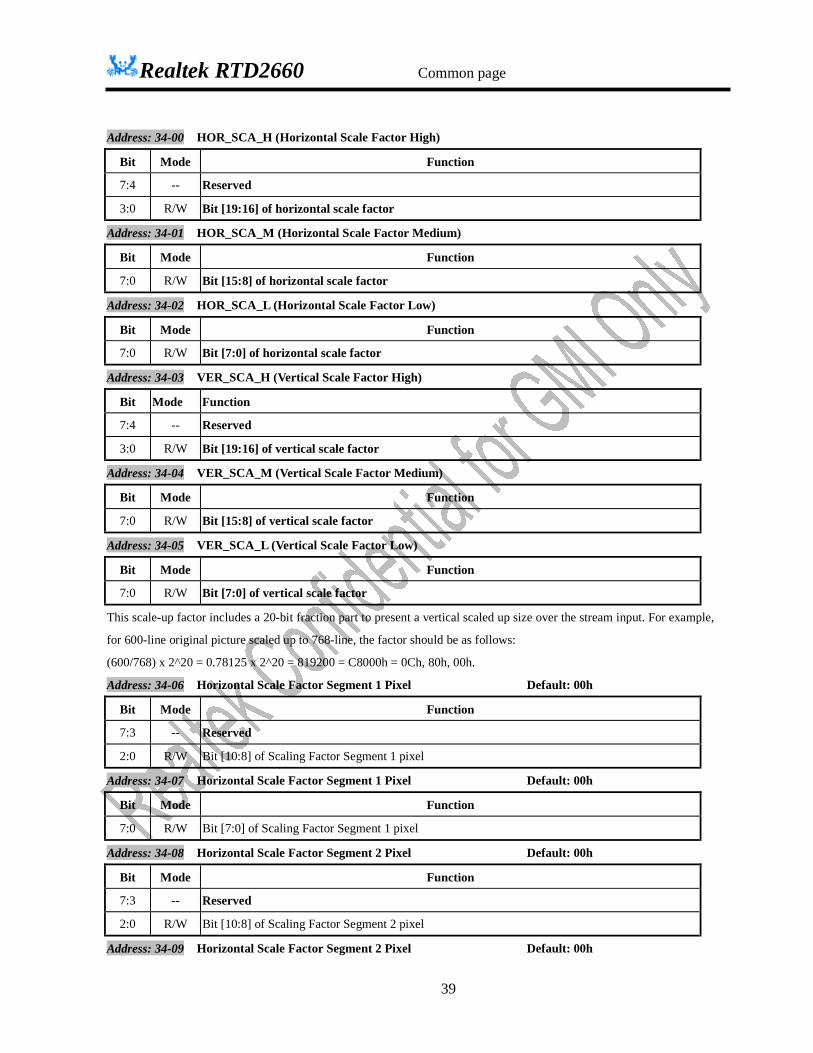
Address: 34-00 HOR_SCA_H (Horizontal Scale Factor High)
Bit Mode Function
7:4 -- Reserved
3:0 R/W Bit [19:16] of horizontal scale factor
Address: 34-01 HOR_SCA_M (Horizontal Scale Factor Medium)
Bit Mode Function
7:0 R/W Bit [15:8] of horizontal scale factor
Address: 34-02 HOR_SCA_L (Horizontal Scale Factor Low)
Bit Mode Function
7:0 R/W Bit [7:0] of horizontal scale factor
Address: 34-03 VER_SCA_H (Vertical Scale Factor High)
Bit Mode Function
7:4 -- Reserved
3:0 R/W Bit [19:16] of vertical scale factor
Address: 34-04 VER_SCA_M (Vertical Scale Factor Medium)
Bit Mode Function
7:0 R/W Bit [15:8] of vertical scale factor
Address: 34-05 VER_SCA_L (Vertical Scale Factor Low)
Bit Mode Function
7:0 R/W Bit [7:0] of vertical scale factor
This scale-up factor includes a 20-bit fraction part to present a vertical scaled up size over the stream input. For example,
for 600-line original picture scaled up to 768-line, the factor should be as follows:
(600/768) x 2^20 = 0.78125 x 2^20 = 819200 = C8000h = 0Ch, 80h, 00h.
Address: 34-06 Horizontal Scale Factor Segment 1 Pixel Default: 00h
Bit Mode Function
7:3 -- Reserved
2:0 R/W Bit [10:8] of Scaling Factor Segment 1 pixel
Address: 34-07 Horizontal Scale Factor Segment 1 Pixel Default: 00h
Bit Mode Function
7:0 R/W Bit [7:0] of Scaling Factor Segment 1 pixel
Address: 34-08 Horizontal Scale Factor Segment 2 Pixel Default: 00h
Bit Mode Function
7:3 -- Reserved
2:0 R/W Bit [10:8] of Scaling Factor Segment 2 pixel
Address: 34-09 Horizontal Scale Factor Segment 2 Pixel Default: 00h
Realtek RTD2660 Common page
40
Bit Mode Function
7:0 R/W Bit [7:0] of Scaling Factor Segment 2 pixel
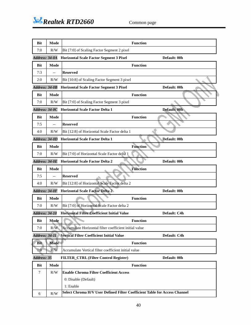
Address: 34-0A Horizontal Scale Factor Segment 3 Pixel Default: 00h
Bit Mode Function
7:3 -- Reserved
2:0 R/W Bit [10:8] of Scaling Factor Segment 3 pixel
Address: 34-0B Horizontal Scale Factor Segment 3 Pixel Default: 00h
Bit Mode Function
7:0 R/W Bit [7:0] of Scaling Factor Segment 3 pixel
Address: 34-0C Horizontal Scale Factor Delta 1 Default: 00h
Bit Mode Function
7:5 -- Reserved
4:0 R/W Bit [12:8] of Horizontal Scale Factor delta 1
Address: 34-0D Horizontal Scale Factor Delta 1 Default: 00h
Bit Mode Function
7:0 R/W Bit [7:0] of Horizontal Scale Factor delta 1
Address: 34-0E Horizontal Scale Factor Delta 2 Default: 00h
Bit Mode Function
7:5 -- Reserved
4:0 R/W Bit [12:8] of Horizontal Scale Factor delta 2
Address: 34-0F Horizontal Scale Factor Delta 2 Default: 00h
Bit Mode Function
7:0 R/W Bit [7:0] of Horizontal Scale Factor delta 2
Address: 34-10 Horizontal Filter Coefficient Initial Value Default: C4h
Bit Mode Function
7:0 R/W Accumulate Horizontal filter coefficient initial value
Address: 34-11 Vertical Filter Coefficient Initial Value Default: C4h
Bit Mode Function
7:0 R/W Accumulate Vertical filter coefficient initial value
Address: 35 FILTER_CTRL (Filter Control Register) Default: 00h
Bit Mode Function
7 R/W Enable Chroma Filter Coefficient Access
0: Disable (Default)
1: Enable
6 R/W Select Chroma H/V User Defined Filter Coefficient Table for Access Channel
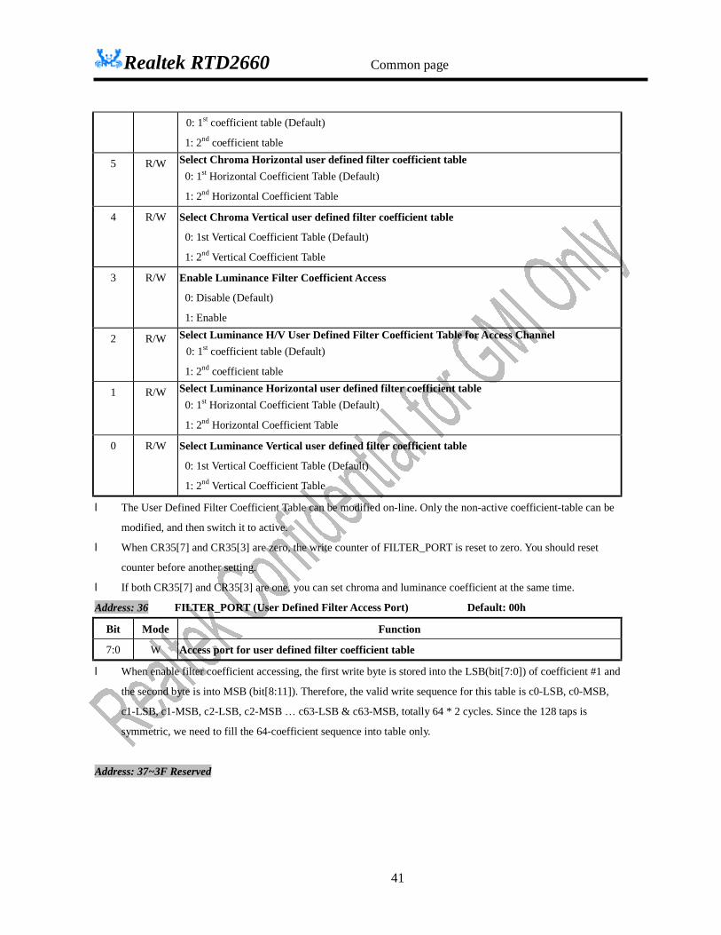
Realtek RTD2660 Common page
41
0: 1st coefficient table (Default)
1: 2nd coefficient table
5 R/W Select Chroma Horizontal user defined filter coefficient table 0: 1st Horizontal Coefficient Table (Default)
1: 2nd Horizontal Coefficient Table
4 R/W Select Chroma Vertical user defined filter coefficient table
0: 1st Vertical Coefficient Table (Default)
1: 2nd Vertical Coefficient Table
3 R/W Enable Luminance Filter Coefficient Access
0: Disable (Default)
1: Enable
2 R/W Select Luminance H/V User Defined Filter Coefficient Table for Access Channel 0: 1st coefficient table (Default)
1: 2nd coefficient table
1 R/W Select Luminance Horizontal user defined filter coefficient table 0: 1st Horizontal Coefficient Table (Default)
1: 2nd Horizontal Coefficient Table
0 R/W Select Luminance Vertical user defined filter coefficient table
0: 1st Vertical Coefficient Table (Default)
1: 2nd Vertical Coefficient Table
l The User Defined Filter Coefficient Table can be modified on-line. Only the non-active coefficient-table can be
modified, and then switch it to active.
l When CR35[7] and CR35[3] are zero, the write counter of FILTER_PORT is reset to zero. You should reset
counter before another setting.
l If both CR35[7] and CR35[3] are one, you can set chroma and luminance coefficient at the same time.
Address: 36 FILTER_PORT (User Defined Filter Access Port) Default: 00h
Bit Mode Function
7:0 W Access port for user defined filter coefficient table
l When enable filter coefficient accessing, the first write byte is stored into the LSB(bit[7:0]) of coefficient #1 and
the second byte is into MSB (bit[8:11]). Therefore, the valid write sequence for this table is c0-LSB, c0-MSB,
c1-LSB, c1-MSB, c2-LSB, c2-MSB … c63-LSB & c63-MSB, totally 64 * 2 cycles. Since the 128 taps is
symmetric, we need to fill the 64-coefficient sequence into table only.
Address: 37~3F Reserved

Realtek RTD2660 Common page
42
Frame Sync Fine Tune
Address: 40 IVS2DVS_DEALY_LINES (IVS to DVS Lines) Default: 00h
Bit Mode Function
7:0 R/W IVS to DVS Lines: (Only for FrameSync Mode)
The number of input HS from IVS to DVS.
Should be double buffer by CR10[5:4]
Address: 41 IV_DV_DELAY_CLK_ODD (Frame Sync Delay Fine Tuning) Default: 00h
Bit Mode Function
7:0 R/W Frame Sync Mode Delay Fine Tune [7:0]
Applied to all fields when Interlaced_FS_Delay_Fine_Tuning is disabled (CR43[1] = 0)
Only for odd-field when Interlaced_FS_Delay_Fine_Tuning is enabled (CR43[1] = 1)
In Frame Sync Mode , CR41[7:0] represents output VS delay fine-tuning. It delays the number of (CR41 [7:0] *16 + 16)
input clocks if CR41[7:0] is not equal to 0. (No delay fine-tune if CR41[7:0] = 0)
Address: 42 IV_DV_DELAY_CLK_EVEN (Frame Sync Delay Fine Tuning) Default: 00h
Bit Mode Function
7:0 R/W Frame Sync Mode Delay Fine Tune [7:0] “00” to disable
Only for even-field when Interlaced_FS_Delay_Fine_Tuning is enabled (CR43[1] = 1)
Address: 43 FS_DELAY_FINE_TUNING Default: 00h
Bit Mode Function
7 R/W Enable measure last line by field
0 : disable
1: enable
6 R/W Reference field in last line measure
0 : 0dd
1 : Even
5:2 R/W Reserved to 0
1 R/W Interlaced_FS_Delay_Fine_Tuning
0: Disable (Default)
1: Enable
0 R/W Internal ODD-signal inverse for Interlaced_FS_Delay_Fine_Tuning
0: No invert (Default)
1: Invert
Address: 44 LAST_LINE_H Default: 00h
Bit Mode Function
7 R/W Last-line-width / DV-Total Selector :

Realtek RTD2660 Common page
43
0: CR44 [3:0] and CR45 indicate last-line width counted by display clock (Default)
1: CR44 [3:0] and CR45 indicate DHS total number between 2 DVS.
6 R/W DV sync with 4X clock
0: Disable
1: Enable
5 R/W BIST Test Enable
0: Disable
1: Enable (Auto clear when finish)
4 R/W BIST Test Result
0: Fail
1: Ok
3:0 R DV Total or Last Line Width[11:8] Before Sync in Frame Sync Mode
Address: 45 LAST_LINE_L
Bit Mode Function
7:0 R DV Total or Last Line Width[7:0] Before Sync in Frame Sync Mode
Address: 46 Reserved as page selector for new sync-processor feature Sync Processor Address: 47 SYNC_SELECT Default: 00h
Bit Mode Function
7 R/W On line Sync Processor Power Down (Stop Crystal Clock In)
0: Normal Run (Default)
1: Power Down
6 R/W HSYNC Type Detection Auto Run
0: manual (Default)
1: automatic
5 R/W De-composite circuit enable
0: Disable (Default)
1: Enable
4 R/W Input Sync. Source selection 0: HS_RAW(SS/CS) (Default) 1: SOG/SOY
3 R/W SOG Source Selection
0: SOG0/SOY0 (Default)
1: SOG1/SOY1
2 R/W VGA-ADC HS/VS Source

Realtek RTD2660 Common page
44
0: 1ST HS/VS (Default)
1: 2ND HS/VS
1 R/W Measured by Crystal Clock (Result shown in CR59) (in Digital Mode)
0: Input Active Region (Vertical IDEN start to IDEN stop) (measure at IDEN STOP) (Default)
1: Display Active Region(Vertical DEN start to DEN stop) (measure at DEN STOP)
The function should work correctly when IVS or DVS occurs and enable by CR50[4].
0 R/W HSYNC & VSYNC Measured Mode
0: HS period counted by crystal clock & VS period counted by HS (Analog mode) (Default)
1: H resolution counted by input clock & V resolution counted by ENA (Digital mode)
(Get the correct resolution which is triggered by enable signal, ENA)
Address: 48 SYNC_INVERT Default: 00h
Bit Mode Function
7 R/W COAST Signal Invert Enable:
0: Not inverted (Default)
1: Inverted
6 R/W COAST Signal Output Enable:
0: Disable (Default)
1: Enable
5 R/W HS_OUT Signal Invert Enable:
0: Not inverted (Default)
1: Inverted
4 R/W HS_OUT Signal Output Enable:
0: Disable (Default)
1: Enable
3 R/W CS_RAW Inverted Enable
0: Normal (Default)
1: Invert
2 R/W CLAMP Signal Output Enable
0: Disable (Default)
1: Enable
1 R/W HS Recovery in Coast
0: Disable (Default) (SS/SOY)
1: Enable (CS or SOG )
0 R/W HSYNC Synchronize source
0: AHS (Default)
1: Feedback HS

Realtek RTD2660 Common page
45
Address: 49 SYNC_CTRL (SYNC Control Register) Default: 06h
Bit Mode Function
7 R/W CLK Inversion to latch Feedback HS for Coast Recovery
( Coast Recovery means HS feedback to replace input HS)
0: Non Inversion (Default)
1: Inversion
6 R/W Select HS_OUT Source Signal
0: Bypass (SeHs)(Use in Separate Mode)
1: Select De-Composite HS out(DeHs) (In Composite mode)
5 R/W Select ADC_VS Source Signal (Auto switch in Auto Run Mode)
0: VS_RAW
1: DeVS
4 R/W CLK Inversion to latch ADC HS for Clamp
0: Non Inversion (Default)
1: Inversion
3 R/W Inversion of HSYNC to measure VSYNC
0: Non Inversion (Default)
1: Inversion
2 R/W HSYNC Measure Source(ADC_HS1)
0: Select ADC_HS
1: Select SeHS or DeHS by CR49[6] (Default)
1:0 R/W Measure HSYNC/VSYNC Source Select:
00: Reserved
01: VIDEO8 / VIDEO16
10: ADC_HS1/ADC_VS (Default)
11: CS_RAW/VS_RAW
Address: 4A STABLE_HIGH_PERIOD_H Default: 00h
Bit Mode Function
7 R Even/Odd Field of YPbPr (By Line-Count Mode)
0: Even
1: Odd
6 R The Toggling of Polarity of YPbPr Field Happened (By Line-Count Mode)
0: No toggle
1: Toggle
5 R Even/Odd Field of YPbPr (By VS-Position Mode)
0: Even

Realtek RTD2660 Common page
46
1: Odd
4 R The Toggling of Polarity of YPbPr Field Happened (By VS-Position Mode)
0: No toggle
1: Toggle
3 R/W Odd Detection Mode
0: Line-Count Mode (Default)
1: VS-Position Mode
2:0 R Stable High Period[10:8]
Compare each line’s high pulse period, if we get continuous 64 lines with the same one, the
period is updated as the stable period.
Address: 4B STABLE_HIGH_PERIOD_L Bit Mode Function 7:0 R Stable High Period[7:0]
Compare each line’s high pulse period, if we get continuous 64 lines with the same one, the period is updated as the stable period.
Address: 4C VSYNC_COUNTER_LEVEL_MSB Default: 03h
Bit Mode Function
7 R HSYNC Type Detection Auto Run Result ready
6:4 R HSYNC Type Detection Auto Run Result 000: No Signal
001: Not Support
010: YPbPr
011: Serration Composite SYNC
100: XOR/OR-Type Composite SYNC with Equalizer
101: XOR/OR-Type Composite SYNC without Equalizer
110: HSYNC with VS_RAW (Separate HSYNC)
111: HSYNC without VS_RAW (HSYNC only)
Reference when Hsync type detection auto run result ready (CR4C[7]) 3 R/W Reserved to 0
2:0 R/W VSYNC counter level count [10:8] MSB
VSYNC detection counter start value.
Address: 4D VSYNC_COUNTER_LEVEL_LSB Default: 00h
Bit Mode Function
7:0 R/W VSYNC counter level count [7:0] LSB
Address: 4E HSYNC_TYPE_DETECTION_FLAG
Bit Mode Function
7 R HSYNC Overflow (16-bits)

Realtek RTD2660 Common page
47
6 R Stable Period Change (write clear when CR4E[6]=1 or CR4F[0]=1)
5 R Stable Polarity Change (write clear when CR4E[5]=1 or CR4F[0]=1)
4 R VS_RAW Edge Occurs (write clear when CR4E[4]=1 or CR4F[0]=1)
If VS_RAW edge occurs, this bit is set to “1”.
3 R Detect Capture Window Unlock Repeated 32 Times (write clear when CR4E[3]=1 or
CR4F[0]=1)
2 R HSYNC with Equalization (write clear when CR4E[2]=1 or CR4F[0]=1)
1 R HSYNC Polarity Change (write clear when CR4E[1]=1 or CR4F[0]=1)
0 R Detect Capture Window Unlock (write clear when CR4E[0]=1 or CR4F[0]=1)
Address: 4F STABLE_MEASURE Default: 00h
Bit Mode Function
7 R Stable Flag
0: Period or polarity can’t get continuous stable status.
1: Both polarity and period are stable.
6 R Stable Polarity
0: Negative
1: Positive
Compare each line’s polarity; if we get continuous N 64 lines with the same one, the polarity is
updated as the stable polarity.
5:4 R/W Feedback HSYNC High Period Select by ADC Clock:
00: 32 (Default)
01: 64
10: 96
11: 128
3 R/W Stable Period Tolerance
0: ±2 crystal clks (Default)
1: ±4 crystal clks
2 R/W VSYNC measure invert Enable
0: Disable (Default)
1: Enable
1 R/W Pop Up Stable Value
0: No Pop Up (Default)
1: Pop Up Result, (CR4A[2:0], CR4B[7:0], CR4E[3], CR50[2:0], CR51[7:0])
0 R/W Stable Measure Start
0 : Stop (Default)
1 : Start

Realtek RTD2660 Common page
48
Address: 50 Stable_Period_H Default: 00h
Bit Mode Function
7 R Measure One Frame Status
0: Finished after 1 frame measuring / Measure finished
1: Measuring Now
6 R CS_RAW Inverted by Auto Run Mode
0: Not inverted
1: Inverted
5 R/W HS_OUT Bypass PLL into VGIP
0: Disable (Default)
1: Enable
4 R/W Active Region Measure Enable
0: Disable (Default)
1: Enable
3 R/W ADC_VS Source Select in Test Mode
0: Select ADC_VS Source in Normal Mode or Auto Mode by CR47[6] (Default)
1: Select ADC_VS Source in Test Mode (Select VS_RAW or DeVS by CR49[5])
2:0 R Stable Period[10:8]
Compare each line’s period, if we get continuous 64 lines with the same one, the period is updated
as the stable period.
Address: 51 Stable_Period_L
Bit Mode Function
7:0 R Stable Period[7:0]
Compare each line’s period, if we get continuous 64 lines with the same one, the period is updated
as the stable period.
Address: 52 MEAS_HS_PER_H (HSYNC Period Measured Result) Default: 8’b000xxxxx
Bit Mode Function
7 R/W Auto Measure Enable
0: Disable (Default)
1: Enable
6 R/W Pop Up Period Measurement Result
0: No Pop Up (Default)
1: Pop Up Result
5 R/W Start a HS & VS period / H & V resolution & polarity measurement (on line monitor)
0: Finished/Disable (Default)
1: Enable to start a measurement, auto cleared after finished

Realtek RTD2660 Common page
49
4 R Over-flow bit of Input HSYNC Period Measurement
0: No Over-flow occurred
1: Over-flow occurred
3:0 R Input HSYNC Period Measurement Result: High Byte[11:8]
Address: 53 MEAS_HS_PER_L (HSYNC Period Measured Result)
Bit Mode Function
7:0 R Input HSYNC Period Measurement Result: Low Byte[7:0]
l The result is expressed as the average number of crystal clocks (CR47[0]=0), or input clocks (CR47[0]=1)
between 2 HSYNC.
l The result is the total number of crystal/input clocks inside 16-HSYNC periods divided by 16.
l Fractional part of measure result is stored in CR56[3:0].
Address: 54 MEAS_VS_PER_H (VSYNC Period Measured Result)
Bit Mode Function
7 R Input VSYNC Polarity Indicator
0: negative polarity (high period is longer than low one)
1: positive polarity (low period is longer than high one)
6 R Input HSYNC Polarity Indicator
0: negative polarity (high period is longer than low one)
1: positive polarity (low period is longer than high one)
5 R Time-Out bit of Input VSYNC Period Measurement (No VSYNC occurred)
0: No Time Out
1: Time Out occurred
4 R Over-flow bit of Input VSYNC Period Measurement
0: No Over-flow occurred
1: Over-flow occurred
3:0 R Input VSYNC Period Measurement Result: High Byte[11:8]
Address: 55 MEAS_VS_PER_L (VSYNC Period Measured Result)
Bit Mode Function
7:0 R Input VSYNC Period Measurement Result: Low Byte[7:0]
l This result is expressed in terms of input HS pulses.
l When measured digitally, the result is expressed as the number of input ENA signal within a frame.
Address: 56 MEAS_HS&VS_HI_H (HSYNC&VSYNC High Period Measured Result)
Bit Mode Function
7:4 R Input HSYNC High Period Measurement Result: High Byte[11:8] (CR58[0] = 0)
Input VSYNC High Period Measurement Result: High Byte[11:8] (CR58[0] = 1)
3:0 R Input HSYNC Period Measurement Fractional Result (See CR52,53)

Realtek RTD2660 Common page
50
Address: 57 MEAS_HS&VS_HI_L (HSYNC&VSYNC High Period Measured Result)
Bit Mode Function
7:0 R Input HSYNC High Period Measurement Result: Low Byte[7:0] (CR58[0] = 0)
Input VSYNC High Period Measurement Result: Low Byte[7:0] (CR58[0] = 1)
l This result of HSYNC high-period is expressed in terms of crystal clocks. When measured digitally, the result of
HSYNC high-period is expressed as the number of input clocks inside the input enable signal.
l This result of VSYNC high-period is expressed in terms of input HS pulses
Address: 58 MEAS_HS&VS_HI_SEL (VSYNC High Period Measured select) Default:02h
Bit Mode Function
7:6 R/W HSYNC_MAX_DELTA
00: Don’t care (CR58[3] will never go high)
01: 4-clock
10: 8-clock
11: 16-clock
5:4 R/W VSYNC_MAX_DELTA
00: Don’t care (CR58[2] will never go high)
01: 2-HSYNC
10: 4-HSYNC
11: 8-HSYNC
3 R HSYNC_OVER_RANGE
Set to 1 if variation of HSYNC larger than HSYNC_MAX_DELTA is detected by on-line
measurement (CR52[7]=1). Write to clear this flag.
2 R VSYNC_OVER_RANGE
Set to 1 if variation of VSYNC larger than VSYNC_MAX_DELTA is detected by on-line
measurement (CR52[7]=1). Write to clear this flag. 1 R/W Start Measurement after Mode Detection Auto-mode
0: Disable 1: Enable (Default)
0 R/W HSYNC/VSYNC High Period Measurement Result Select
0: HSYNC
1: VSYNC
(See CR56~CR57)
Address: 59 MEAS_ACTIVE_REGION_H (Active Region Measured by CRSTL_CLK Result)
Bit Mode Function
7:0 R/W Active Region Measured By Crystal Clock
1st read: Measurement Result: High Byte[23:16]
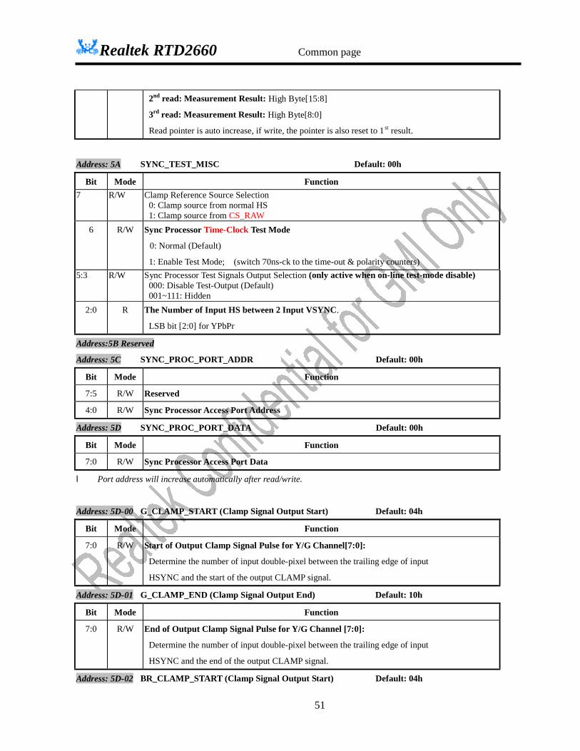
Realtek RTD2660 Common page
51
2nd read: Measurement Result: High Byte[15:8]
3rd read: Measurement Result: High Byte[8:0]
Read pointer is auto increase, if write, the pointer is also reset to 1 st result.
Address: 5A SYNC_TEST_MISC Default: 00h
Bit Mode Function 7 R/W Clamp Reference Source Selection
0: Clamp source from normal HS 1: Clamp source from CS_RAW
6 R/W Sync Processor Time-Clock Test Mode
0: Normal (Default)
1: Enable Test Mode; (switch 70ns-ck to the time-out & polarity counters) 5:3 R/W Sync Processor Test Signals Output Selection (only active when on-line test-mode disable)
000: Disable Test-Output (Default) 001~111: Hidden
2:0 R The Number of Input HS between 2 Input VSYNC.
LSB bit [2:0] for YPbPr
Address:5B Reserved Address: 5C SYNC_PROC_PORT_ADDR Default: 00h
Bit Mode Function
7:5 R/W Reserved
4:0 R/W Sync Processor Access Port Address
Address: 5D SYNC_PROC_PORT_DATA Default: 00h
Bit Mode Function
7:0 R/W Sync Processor Access Port Data
l Port address will increase automatically after read/write.
Address: 5D-00 G_CLAMP_START (Clamp Signal Output Start) Default: 04h
Bit Mode Function
7:0 R/W Start of Output Clamp Signal Pulse for Y/G Channel[7:0]:
Determine the number of input double-pixel between the trailing edge of input
HSYNC and the start of the output CLAMP signal.
Address: 5D-01 G_CLAMP_END (Clamp Signal Output End) Default: 10h
Bit Mode Function
7:0 R/W End of Output Clamp Signal Pulse for Y/G Channel [7:0]:
Determine the number of input double-pixel between the trailing edge of input
HSYNC and the end of the output CLAMP signal.
Address: 5D-02 BR_CLAMP_START (Clamp Signal Output Start) Default: 04h
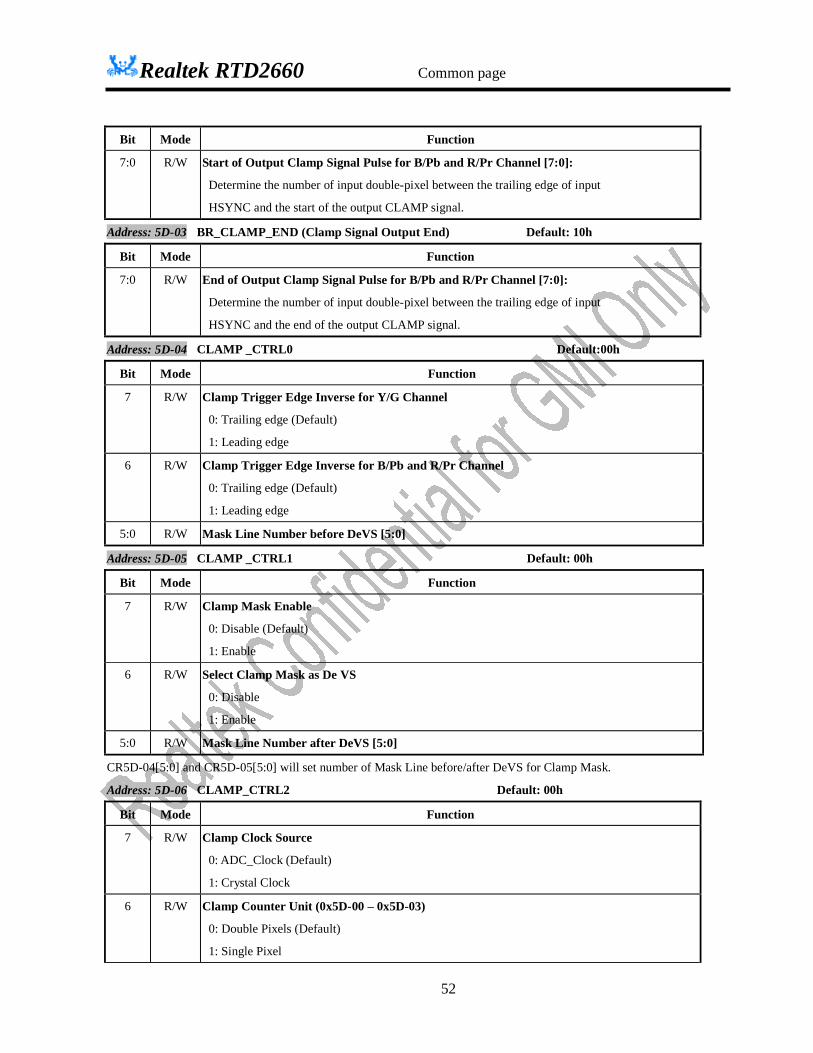
Realtek RTD2660 Common page
52
Bit Mode Function
7:0 R/W Start of Output Clamp Signal Pulse for B/Pb and R/Pr Channel [7:0]:
Determine the number of input double-pixel between the trailing edge of input
HSYNC and the start of the output CLAMP signal.
Address: 5D-03 BR_CLAMP_END (Clamp Signal Output End) Default: 10h
Bit Mode Function
7:0 R/W End of Output Clamp Signal Pulse for B/Pb and R/Pr Channel [7:0]:
Determine the number of input double-pixel between the trailing edge of input
HSYNC and the end of the output CLAMP signal.
Address: 5D-04 CLAMP _CTRL0 Default:00h
Bit Mode Function
7 R/W Clamp Trigger Edge Inverse for Y/G Channel
0: Trailing edge (Default)
1: Leading edge
6 R/W Clamp Trigger Edge Inverse for B/Pb and R/Pr Channel
0: Trailing edge (Default)
1: Leading edge
5:0 R/W Mask Line Number before DeVS [5:0]
Address: 5D-05 CLAMP _CTRL1 Default: 00h
Bit Mode Function
7 R/W Clamp Mask Enable
0: Disable (Default)
1: Enable
6 R/W Select Clamp Mask as De VS
0: Disable
1: Enable
5:0 R/W Mask Line Number after DeVS [5:0]
CR5D-04[5:0] and CR5D-05[5:0] will set number of Mask Line before/after DeVS for Clamp Mask.
Address: 5D-06 CLAMP_CTRL2 Default: 00h
Bit Mode Function
7 R/W Clamp Clock Source
0: ADC_Clock (Default)
1: Crystal Clock
6 R/W Clamp Counter Unit (0x5D-00 – 0x5D-03)
0: Double Pixels (Default)
1: Single Pixel

Realtek RTD2660 Common page
53
5 R/W Off-line ADC Clamp Enable
0: Disable (Default)
1: Enable
4 R/W Off-line ADC Selection
0: ADC-0 (Default)
1: ADC-1
3 R/W On-Line ADC-3 Clamp Source
0: Clamp-G (Default)
1: Clamp-BR
3 R/W On-Line ADC-2 Clamp Source
0: Clamp-G (Default)
1: Clamp-BR
3 R/W On-Line ADC-1 Clamp Source
0: Clamp-G (Default)
1: Clamp-BR
3 R/W On-Line ADC-0 Clamp Source
0: Clamp-G (Default)
1: Clamp-BR
Address: 5D-07 COAST_CTRL Default: 21h
Bit Mode Function
7:4 R/W Start of COAST before DeVS Leading Edge [3:0]
3:0 R/W End of COAST after DeVS Trailing Edge [3:0]
Address: 5D-08 CAPTURE_WINDOW_SETTING Default: 04h
Bit Mode Function
7 R/W Reserved to 0
6 R/W Capture Miss Limit during Hsync Extraction
0: 32 (Default)
1: 16
5 R/W Capture Window add step as Miss Lock
0: ±1 crystal clks (Default)
1: ±2 crystal clks 4:0 R/W Capture Window Tolerance
5’h00: ±6 crystal clks for capture window 5’h01 ~ 5’b1F : ±1 ~ ±31 crystal clks for capture window
Address: 5D-09 DETECTION_TOLERANCE_SETTING Default: 00h
Bit Mode Function
7 R/W Reserved to 0
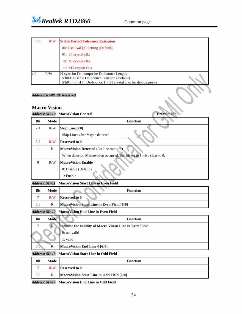
Realtek RTD2660 Common page
54
6:5 R/W Stable Period Tolerance Extension
00: Use 0x4F[3] Setting (Default)
01: ±4 crystal clks
10: ±8 crystal clks
11: ±16 crystal clks 4:0 R/W H-sync for De-composite De-bounce Length
5’h00: Disable De-bounce Function (Default) 5’h01 ~ 5’h1F : De-bounce 1 ~ 31 crystal clks for de-composite
Address:5D-08~0F Reserved
Macro Vision Address: 5D-10 MacroVision Control Default: 00h
Bit Mode Function
7:4 R/W Skip Line[3:0]
Skip Lines after Vsync detected
3:2 R/W Reserved to 0
1 R MacroVision Detected (On-line monitor)
When detected Macrovision occurred, this bit set to 1, else clear to 0.
0 R/W MacroVision Enable
0: Disable (Default)
1: Enable
Address: 5D-11 MacroVision Start Line in Even Field
Bit Mode Function
7 R/W Reserved to 0
6:0 R MacroVision Start Line in Even Field [6:0]
Address: 5D-12 MacroVision End Line in Even Field
Bit Mode Function
7 R Indicate the validity of Macro Vision Line in Even Field
0: not valid
1: valid
6:0 R MacroVision End Line 0 [6:0]
Address: 5D-13 MacroVision Start Line in Odd Field
Bit Mode Function
7 R/W Reserved to 0
6:0 R MacroVision Start Line in Odd Field [6:0]
Address: 5D-14 MacroVision End Line in Odd Field

Realtek RTD2660 Common page
55
Bit Mode Function
7 R Indicate the validity of Macro Vision Line in Odd Field
0: not valid
1: valid
6:0 R MacroVision End Line in Odd Field [6:0]
Address: 5D-15 Macro Vision Detect De-bounce Default: 00h
Bit Mode Function
7:5 R/W Reserved to 0 4:0 R/W H-sync for Macro-Vision Detection De-bounce Length
5’h00 ~ 5’h07: De-bounce 7 crystal clks for de-composite (Default) 5’h08 ~ 5’h1F: De-bounce 8 ~ 31 crystal clks for de-composite
Address 0x5E is reserved
Highlight window
Address: 60 Highlight Window Access Port control Default: 00h
Bit Mode Function
7 R/W Enable highlight window access port
6 R/W Enable highlight window
5:4 -- Reserved
3:0 R/W Highlight-window port address
Address: 61-00 Highlight Window Horizontal Start
Bit Mode Function
7:0 -- Reserved
2:0 R/W Highlight window horizontal start[10:8]
Address: 61-01 Highlight Window Horizontal Start
Bit Mode Function
7:0 R/W Highlight window horizontal start[7:0]
Address: 61-02 Highlight Window Horizontal End
Bit Mode Function
7:3 -- Reserved
2:0 R/W Highlight window horizontal end[10:8]
Address: 61-03 Highlight Window Horizontal End
Bit Mode Function
7:0 R/W Highlight window horizontal end[7:0]

Realtek RTD2660 Common page
56
Address: 61-04 Highlight Window Vertical Start
Bit Mode Function
7:3 -- Reserved
2:0 R/W Highlight window vertical start[10:8]
Address: 61-05 Highlight Window Vertical Start
Bit Mode Function
7:0 R/W Highlight window vertical start[7:0]
Address: 61-06 Highlight Window Vertical End
Bit Mode Function
7:3 -- Reserved
2:0 R/W Highlight window vertical end[10:8]
Address: 61-07 Highlight Window Vertical End
Bit Mode Function
7:0 R/W Highlight window vertical end[7:0]
Highlight window horizontal/vertical reference point is DEN (display background start).
Address: 61-08 Highlight Window Border
Bit Mode Function
7:4 -- Reserved
3:0 R/W Highlight window border width
Address: 61-09 Highlight Window Border Color
Bit Mode Function
7:6 -- Reserved
5:0 R/W Highlight window border red color MSB 6bit (red color 2-bit LSB = 00)
Address: 61-0A Highlight Window Border Color
Bit Mode Function
7:6 -- Reserved
5:0 R/W Highlight window border green color MSB 6bit (green color 2-bit LSB = 00)
Address: 61-0B Highlight Window Border Color
Bit Mode Function
7:6 -- Reserved
5:0 R/W Highlight window border blue color MSB 6bit (blue color 2-bit LSB = 00)
Address: 61-0C Highlight Window Control 0 Default : 00h
Bit Mode Function
7:6 R/W Contrast / brightness application control
00: Set A used on full region
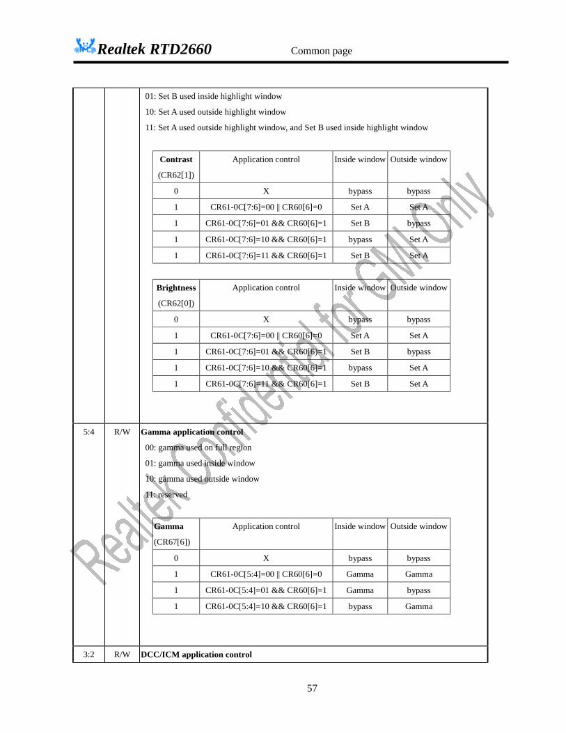
Realtek RTD2660 Common page
57
01: Set B used inside highlight window
10: Set A used outside highlight window
11: Set A used outside highlight window, and Set B used inside highlight window
Contrast
(CR62[1])
Application control Inside window Outside window
0 X bypass bypass
1 CR61-0C[7:6]=00 || CR60[6]=0 Set A Set A
1 CR61-0C[7:6]=01 && CR60[6]=1 Set B bypass
1 CR61-0C[7:6]=10 && CR60[6]=1 bypass Set A
1 CR61-0C[7:6]=11 && CR60[6]=1 Set B Set A
Brightness
(CR62[0])
Application control Inside window Outside window
0 X bypass bypass
1 CR61-0C[7:6]=00 || CR60[6]=0 Set A Set A
1 CR61-0C[7:6]=01 && CR60[6)=1 Set B bypass
1 CR61-0C[7:6]=10 && CR60[6]=1 bypass Set A
1 CR61-0C[7:6]=11 && CR60[6]=1 Set B Set A
5:4 R/W Gamma application control
00: gamma used on full region
01: gamma used inside window
10: gamma used outside window
11: reserved
Gamma
(CR67[6])
Application control Inside window Outside window
0 X bypass bypass
1 CR61-0C[5:4]=00 || CR60[6]=0 Gamma Gamma
1 CR61-0C[5:4]=01 && CR60[6]=1 Gamma bypass
1 CR61-0C[5:4]=10 && CR60[6]=1 bypass Gamma
3:2 R/W DCC/ICM application control

Realtek RTD2660 Common page
58
00: DCC/ICM used on full region
01: DCC/ICM used inside window
10: DCC/ICM used outside window
11: Reserved
ICM
(CRE0[7])
Application control Inside window Outside window
0 X bypass bypass
1 CR61-0C[3:2]=00 || CR60[6]=0 ICM ICM
1 CR61-0C[3:2]=01 && CR60[6]=1 ICM bypass
1 CR61-0C[3:2]=10 && CR60[6]=1 bypass ICM
DCC
(CRE4[7])
Application control Inside window Outside window
0 X bypass bypass
1 CR61-0C[3:2]=00 || CR60[6]=0 DCC DCC
1 CR61-0C[3:2]=01 && CR60[6]=1 DCC bypass
1 CR61-0C[3:2]=10 && CR60[6]=1 bypass DCC 1:0 R/W /DLTI/DCTI/Peaking/Coring application control
00:Full region
01: Inside window
10: Outside window
11: Reserved
Peaking
(CR9A[6])
Application control Inside window Outside window
0 X bypass bypass
1 CR61-0C[5:4]=00 || CR60[6]=0 Peaking Peaking
1 CR61-0C[5:4]=01 && CR60[6]=1 Peaking bypass
1 CR61-0C[5:4]=10 && CR60[6]=1 bypass Peaking
Address: 61-0D Highlight Window Control 1 Default : 00h
Bit Mode Function

Realtek RTD2660 Common page
59
7:6 R/W sRGB application control
00: sRGB used on full region
01: sRGB used inside highlight window
10: sRGB used outside highlight window
11: Reserved
sRGB
(CR62[2])
Application control Inside window Outside window
0 X bypass bypass
1 CR61-0D[7:6]=00 || CR60[6]=0 sRGB sRGB
1 CR61-0D[7:6]=01 && CR60[6]=1 sRGB bypass
1 CR61-0D[7:6]=10 && CR60[6]=1 bypass sRGB
5:0 -- Reserved to 0
Inside window left-top point = (horizontal start + border width, vertical start + border width) Inside window right-bottom point = (horizontal end, vertical end) Border window left-top point = (horizontal start, vertical start) Border window right-bottom point = (horizontal end+ border width, vertical end + border width) Border = border window – inside window Outside window = screen – border window
(horizontal start, vertical start)
(horizontal end, vertical end)
Border width
Inside window
border

Realtek RTD2660 Common page
60
Color Processor Control Address: 62 COLOR_CTRL (Color Control Register) Default: 00h
Bit Mode Function
7 R/W sRGB Coefficient Write Ready
0: Not ready or cleared after finished
1: Ready to write (wait for DVS to apply)
6 R/W sRGB Precision
0: Normal (Default)
1: Multiplier Coefficient Bit Left Shift
5:3 R/W sRGB Coefficient Write Enable
000: Disable
001: Write R Channel (RRH,RRL,RGH,RGL,RBH,RBL) (address reset to 0 when written)
010: Write G Channel (GRH,GBL,GGH,GGL,GBH,GBL) (address reset to 0 when written)
011: Write B Channel (BRH,BRL,BGH,BGL,BBH,BBL) (address reset to 0 when written)
100: R Offset
101: G Offset
110: B Offset
2 R/W Enable sRGB Function
0: Disable (Default)
1: Enable
1 R/W Enable Contrast Function:
0: disable the coefficient (Default)
1: enable the coefficient
0 R/W Enable Brightness Function:
0: disable the coefficient (Default)
1: enable the coefficient
Address: 63 SRGB_ACCESS_PORT
Bit Mode Function
7:0 W sRGB_COEF[7:0]
l For Multiplier coefficient: 9 bit: 1 bit sign, 8 bit fractional part
l For filling multiplier coefficient, the sequence should be SIGN bit (High Byte), 8 bit fractional (Low Byte)
l For Offset Coefficient: 1 sign, 5 integer, 2 bit fractional part
l sRGB output saturation to 1023 and Clamp to 0
l sRGB Output is 10 bit

Realtek RTD2660 Common page
61
+++
++
+=
BoffsetBGoffsetGRoffsetR
BBBGBRGBGGGRRBRGRR
BGR
11
1
'
'
'
Contrast/Brightness Coefficient
Address: 64 Contrast /Brightness Access Port Control Default: 00h
Bit Mode Function
7 R/W Enable Contrast /Brightness access port
6 R/W sRGB multiplier coefficient precision
0: 1-bit Shift-left (Default)
1: 2-bit Shift-left
5:4 -- Reserved
3:0 R/W Contrast /Brightness port address
Access data port continuously will get address auto increase.
Address: 65-00 BRI_RED_COE (Set A)
Bit Mode Function
7:0 R/W Brightness Red Coefficient:
Valid range: -128(00h) ~ 0(80h) ~ +127(FFh)
Address: 65-01 BRI_GRN_COE (Set A)
Bit Mode Function
7:0 R/W Brightness Green Coefficient: Valid range:
Valid range: -128(00h) ~ 0(80h) ~ +127(FFh)
Address: 65-02 BRI_BLU_COE (Set A)
Bit Mode Function
7:0 R/W Brightness Blue Coefficient:
Valid range: -128(00h) ~ 0(80h) ~ +127(FFh)
Address: 65-03 CTS_RED_COE (Set A)
Bit Mode Function
7:0 R/W Contrast Red Coefficient:
Valid range: 0(00h) ~ 1(80h) ~ 2(FFh)
Address: 65-04 CTS_GRN_COE (Set A)
Bit Mode Function
7:0 R/W Contrast Green Coefficient:
Valid range: 0(00h) ~ 1(80h) ~ 2(FFh)
Address: 65-05 CTS_BLU_COE (Set A)

Realtek RTD2660 Common page
62
Bit Mode Function
7:0 R/W Contrast Blue Coefficient:
Valid range: 0(00h) ~ 1(80h) ~ 2(FFh)
Address: 65-06 BRI_RED_COE (Set B)
Bit Mode Function
7:0 R/W Brightness Red Coefficient:
Valid range: -128(00h) ~ 0(80h) ~ +127(FFh)
Address: 65-07 BRI_GRN_COE (Set B)
Bit Mode Function
7:0 R/W Brightness Green Coefficient: Valid range:
Valid range: -128(00h) ~ 0(80h) ~ +127(FFh)
Address: 65-08 BRI_BLU_COE (Set B)
Bit Mode Function
7:0 R/W Brightness Blue Coefficient:
Valid range: -128(00h) ~ 0(80h) ~ +127(FFh)
Address: 65-09 CTS_RED_COE (Set B)
Bit Mode Function
7:0 R/W Contrast Red Coefficient:
Valid range: 0(00h) ~ 1(80h) ~ 2(FFh)
Address: 65-0A CTS_GRN_COE (Set B)
Bit Mode Function
7:0 R/W Contrast Green Coefficient:
Valid range: 0(00h) ~ 1(80h) ~ 2(FFh)
Address: 65-0B CTS_BLU_COE (Set B)
Bit Mode Function
7:0 R/W Contrast Blue Coefficient:
Valid range: 0(00h) ~ 1(80h) ~ 2(FFh)
When highlight window is disable, coefficient set A is used.
Gamma Control Address: 66 GAMMA_PORT
Bit Mode Function
7:0 W Access port for gamma correction table Address: 67 GAMMA_CTRL Default: 00h
Bit Mode Function
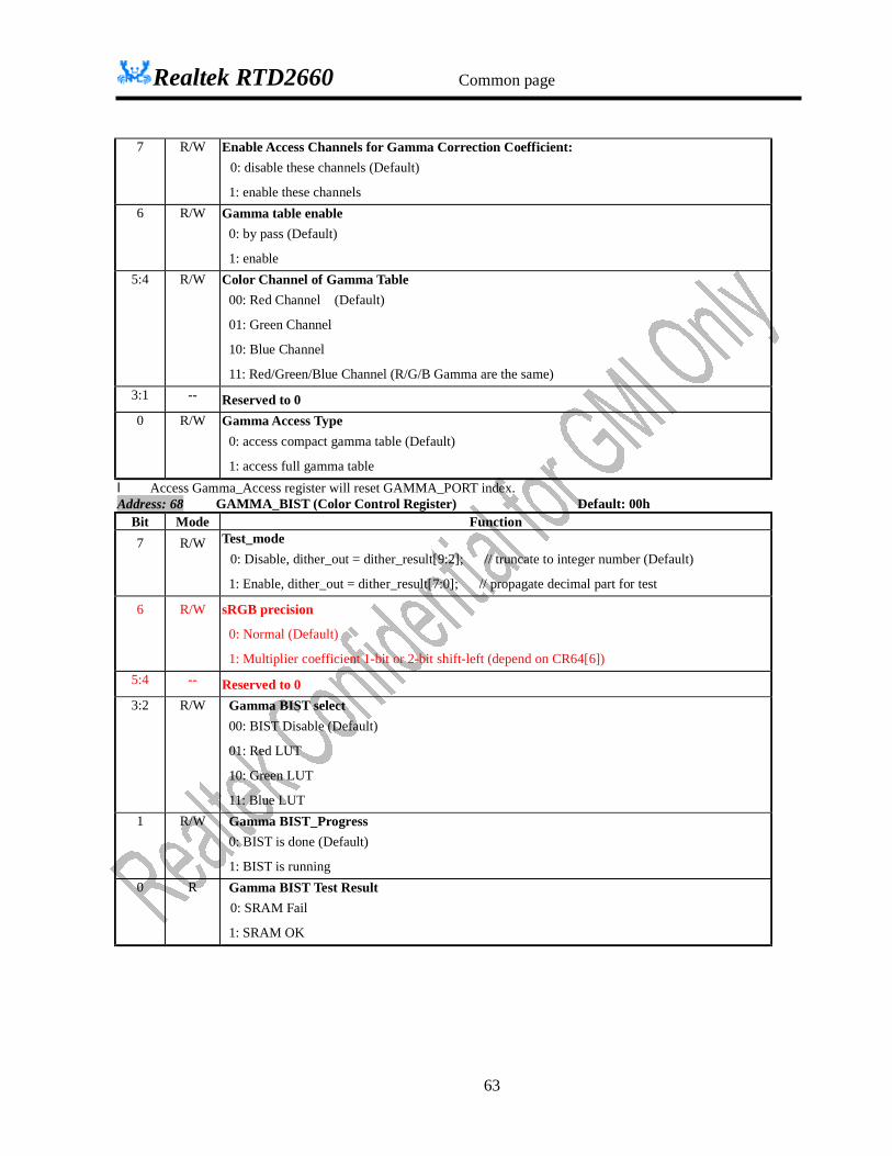
Realtek RTD2660 Common page
63
7 R/W Enable Access Channels for Gamma Correction Coefficient: 0: disable these channels (Default)
1: enable these channels 6 R/W Gamma table enable
0: by pass (Default)
1: enable 5:4 R/W Color Channel of Gamma Table
00: Red Channel (Default)
01: Green Channel
10: Blue Channel
11: Red/Green/Blue Channel (R/G/B Gamma are the same) 3:1 -- Reserved to 0 0 R/W Gamma Access Type
0: access compact gamma table (Default)
1: access full gamma table l Access Gamma_Access register will reset GAMMA_PORT index. Address: 68 GAMMA_BIST (Color Control Register) Default: 00h
Bit Mode Function 7 R/W Test_mode
0: Disable, dither_out = dither_result[9:2]; // truncate to integer number (Default)
1: Enable, dither_out = dither_result[7:0]; // propagate decimal part for test
6 R/W sRGB precision
0: Normal (Default)
1: Multiplier coefficient 1-bit or 2-bit shift-left (depend on CR64[6]) 5:4 -- Reserved to 0 3:2 R/W Gamma BIST select
00: BIST Disable (Default)
01: Red LUT
10: Green LUT
11: Blue LUT 1 R/W Gamma BIST_Progress
0: BIST is done (Default)
1: BIST is running 0 R Gamma BIST Test Result
0: SRAM Fail
1: SRAM OK

Realtek RTD2660 Common page
64
Dithering Control Register:: DITHERING_DATA_ACCESS 0x69
Name Bits Read/ Write
Reset State Comments Config
DITHERING_DATA_ACCESS
7:0 W 0 Refer to following description
Register:: DITHERING_CTRL1 0x6A
Name Bits Read/ Write
Reset State Comments Config
Dither_Access 7:6 R/W 0 Enable Access Control 00: disable (Default)
01: enable access dithering sequence table
10: enable access dithering table
11: enable access temporal offset
Dither_en 5 R/W 0 Enable Dithering Function 0: disable (Default)
1: enable
Dither_temp 4 R/W 0 Temporal Dithering
0: Disable (Default)
1: Enable
Dither_table 3 R/W 0 Dithering Table Value Sign
0: unsigned
1: signed (2’s complement)
Dither_mode 2 R/W 0 Dithering Mode
0: New (Default)
1: Old
Dither_V_Fram_M 1 R/W 0 Vertical Frame Modulation
0: Disable (Default)
1: Enable
Dither_VH_Fram_M
0 R/W 0 Horizontal Frame Modulation
0: Disable (Default)
1: Enable
Address 0x6B is reserved Overlay/Color Palette/Background Color Control Address: 6C OVERLAY_CTRL (Overlay Display Control Register) Default: 00h
Bit Mode Function
7:6 -- Reserved to 0
5 R/W Background color access enable
0: Disable(Reset CR6D Write Pointer to R)
Realtek RTD2660 Common page
65
1: Enable
4:2 R/W Alpha blending level (Also enable OSD frame control register 0x003 byte 1[3:2]
000: Disable (Default)
001 ~111: 1/8~ 7/8
1 R/W Overlay Sampling Mode Select:
0: single pixel per clock (Default)
1: dual pixels per clock (The OSD will be zoomed 2X in horizontal scan line)
0 R/W Overlay Port Enable:
0: Disable (Default)
1: Enable
Turn off overlay enable and switch to background simultaneously when auto switch to
background.
Address: 6D BGND_COLOR_CTRL Default: 00h
Bit Mode Function
7:0 R/W Background color RGB 8-bit value[7:0]
l There are 3 bytes color select of background R, G, B, once we enable Background color access channel(CR6C[5]
and the continuous writing sequence is R/G/B
Address: 6E OVERLAY_LUT_ADDR (Overlay LUT Address) Default: 00h
Bit Mode Function
7 R/W Enable Overlay Color Plate Access:
0: Disable (Default)
1: Enable
6 R/W Reserved to 0
5:0 R/W Overlay 16x24 Look-Up-Table Write Address [5:0]
l Auto-increment while every accessing “Overlay LUT Access Port”.
Address: 6F COLOR_LUT_PORT (LUT Access Port)
Bit Mode Function
7:0 W Color Palette 16x24 Look-Up-Table access port [7:0]
l Using this port to access overlay color plate which addressing by the above registers.
l The writing sequence into LUT is [R0, G0, B0, R1, G1, B1, … R15, G15, and B15] and the address counter will
be automatic increment and circular from 0 to 47.
Image Auto Function
Address: 70 H_BOUNDARY_H
Bit Mode Function
7 -- Reserved

Realtek RTD2660 Common page
66
6:4 R/W Horizontal Boundary Start: High Byte [10:8]
3:0 R/W Horizontal Boundary End: High Byte [11:8]
Address: 71 H_BOUNDARY_STA_L
Bit Mode Function
7:0 R/W Horizontal Boundary Start: Low Byte [7:0]
Address: 72 H_BOUNDARY_END_L
Bit Mode Function
7:0 R/W Horizontal Boundary End: Low Byte [7:0]
Address: 73 V_BOUNDARY_H
Bit Mode Function
7 -- Reserved
6:4 R/W Vertical Boundary Start: High Byte [10:8]
3:0 R/W Vertical Boundary End: High Byte [11:8]
Vertical boundary search should be limited by Vertical boundary start.
Address: 74 V_BOUNDARY_STA_L
Bit Mode Function
7:0 R/W Vertical Boundary Start: Low Byte [7:0]
Address: 75 V_BOUNDARY_END_L
Bit Mode Function
7:0 R/W Vertical Boundary End: Low Byte [7:0]
Address: 76 RED_NOISE_MARGIN (Red Noise Margin Register)
Bit Mode Function
7:2 R/W Red pixel noise margin setting register
1:0 -- Reserved to 0
Address: 77 GRN_NOISE_MARGIN (Green Noise Margin Register)
Bit Mode Function
7:2 R/W Green pixel noise margin setting register
1:0 -- Reserved to 0
Address: 78 BLU_NOISE_MARGIN (Blue Noise Margin Register)
Bit Mode Function
7:2 R/W Blue pixel noise margin setting register
1:0 -- Reserved to 0
Address: 79 DIFF_THRESHOLD
Bit Mode Function

Realtek RTD2660 Common page
67
7:0 R/W Difference Threshold
(Threshold for DIFF no matter CR7D[2] = 0 or 1)
Address: 7A AUTO_ADJ_CTRL0 Default: 00h
Bit Mode Function
7 R/W Field_Select_Enable: Auto-Function only active when Even or Odd field.
0: Disable (Default)
1: Enable
6 R/W Field_Select: Select Even or Odd field. Active when Field_Select_Enable.
0: Active when ODD signal is “0” (Default)
1: Active when ODD signal is “1”
5 R/W Low Pass Filter (121-LPF)
0: Disable (Default)
1: Enable
4 R/W Auto Function Acceleration :
0: Disable (Default)
1: Enable
For auto-balance (CR7D[1]=0), this function must be disabled.
3:2 R/W Vertical boundary search:
00: 1 pixel over threshold (Default)
01: 2 pixel over threshold
10: 4 pixel over threshold
11: 8 pixel over threshold
1:0 R/W Color Source Select for Detection:
00: B color (Default)
01: G color
10: R color
11: ALL ( the result will be divided by 2 )
Address: 7B HW_AUTO_PHASE_CTRL0 Default: 00h
Bit Mode Function
7:3 R/W Number of Auto-Phase Step (Valut+1)
(How many times (steps reference CR7B[2:0]) jumps when using Hardware Auto)
2:0 R/W Hardware Auto Phase Step
000: Step =1 (Default)
001 Step =2
010: Step =4
011: Step =8
Realtek RTD2660 Common page
68
1xx: Step =16
Address: 7C HW_AUTO_PHASE_CTRL1 Default: 00h
Bit Mode Function
7 R/W Hardware Auto Phase Select Trigger
0: IVS
1: Vertical Boundary End
6:0 R/W Initial phase of Auto-Phase (0~127)
Address: 7D AUTO_ADJ_CTRL1 Default: 00h
Bit Mode Function
7 R/W Measure Digital Enable Info when boundary search active
0: Normal Boundary Search (Default)
1: Digital Enable Info Boundary Search.(Digital mode)
6 R/W Hardware / Software Auto Phase Switch
0: Software (Default)
1: Hardware
5 R/W Color Max or Min Measured Select:
0: MIN color measured (Only when Balance-Mode, result must be complemented) (Default)
1: MAX color measured
4 R/W Accumulation or Compare Mode
0: Compare Mode (Default)
1: Accumulation Mode
3 R/W Mode Selection For SOD
0: SOD Edge Mode (Default)
1: SOD Edge + Pulse Mode
2 R/W Type Selection For DIFF
0: DIFF
1: (DIFF/4) * (DIFF/4)
Total result for each color is divided by 8 if this bit is 1.
1 R/W Function (Phase/Balance) Selection
0: Auto-Balance (Default)
1: Auto-Phase
0 R/W Start Auto-Function Tracking Function:
0: stop or finished (Default)
1: start
Realtek RTD2660 Common page
69
Control Table/ Function Sub-Function CR7D.6 CR7D.5 CR7D.4 CR7D.3 CR7D.1 CR7C
Auto-Balance Max pixel X 1 0 0 0 X
Min pixel X 0 0 0 0 X
Auto-Phase Type Mode1 1 1 1 0 1 Th
Mode2 1 1 1 1 1 Th
Accumulation All pixel 1 1 1 0 0 0
Table 1 Auto-Tracking Control Table
Address: 7E VER_START_END_H (Active region vertical start Register)
Bit Mode Function
7:4 R Active region vertical START measurement result: bit[11:8]
3:0 R Active region vertical END measurement result: bit[11:8]
Address: 7F VER_START_L (Active region vertical start Register)
Bit Mode Function
7:0 R Active region vertical start measurement result: bit[7:0]
Address: 80 VER_END_L (Active region vertical end Register)
Bit Mode Function
7:0 R Active region vertical end measurement result: bit[7:0]
Address: 81 H_START_END_H (Active region horizontal start Register)
Bit Mode Function
7:4 R Active region horizontal START measurement result: bit [11:8]
3:0 R Active region horizontal END measurement result: bit[11:8]
Address: 82 H_START_L (Active region horizontal start Register)
Bit Mode Function
7:0 R Active region horizontal start measurement result: bit[7:0]
Address: 83 H_END_L (Active region horizontal end Register)
Bit Mode Function
7:0 R Active region horizontal end measurement result: bit[7:0]
Address: 84 AUTO_PHASE_3 (Auto phase result byte3 register)
Bit Mode Function
7:0 R Auto phase measurement result: bit[31:24]
Address: 85 AUTO_PHASE_2 (Auto phase result byte2 register)
Bit Mode Function
7:0 R Auto phase measurement result: bit[23:16]
Address: 86 AUTO_PHASE_1 (Auto phase result byte1 register)
Realtek RTD2660 Common page
70
Bit Mode Function
7:0 R Auto phase measurement result: bit[15:8]
Address: 87 AUTO_PHASE_0 (Auto phase result byte0 register)
Bit Mode Function
7:0 R Auto phase measurement result: bit[7:0]
The measured value of R or G or B color max or min. (Auto-Balance)
Address 0x88~0x8A are reserved
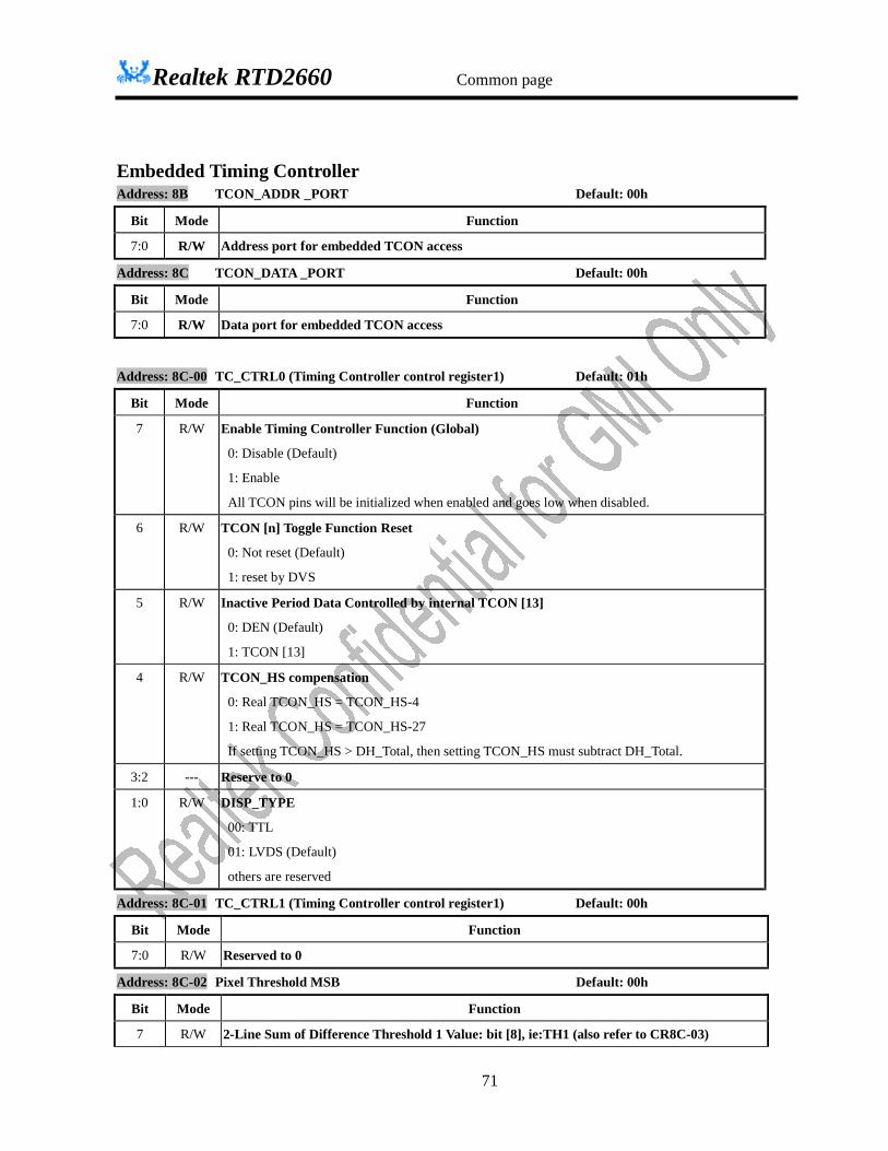
Realtek RTD2660 Common page
71
Embedded Timing Controller Address: 8B TCON_ADDR _PORT Default: 00h
Bit Mode Function
7:0 R/W Address port for embedded TCON access
Address: 8C TCON_DATA _PORT Default: 00h
Bit Mode Function
7:0 R/W Data port for embedded TCON access
Address: 8C-00 TC_CTRL0 (Timing Controller control register1) Default: 01h
Bit Mode Function
7 R/W Enable Timing Controller Function (Global)
0: Disable (Default)
1: Enable
All TCON pins will be initialized when enabled and goes low when disabled.
6 R/W TCON [n] Toggle Function Reset
0: Not reset (Default)
1: reset by DVS
5 R/W Inactive Period Data Controlled by internal TCON [13]
0: DEN (Default)
1: TCON [13]
4 R/W TCON_HS compensation
0: Real TCON_HS = TCON_HS-4
1: Real TCON_HS = TCON_HS-27
If setting TCON_HS > DH_Total, then setting TCON_HS must subtract DH_Total.
3:2 --- Reserve to 0
1:0 R/W DISP_TYPE
00: TTL
01: LVDS (Default)
others are reserved
Address: 8C-01 TC_CTRL1 (Timing Controller control register1) Default: 00h
Bit Mode Function
7:0 R/W Reserved to 0
Address: 8C-02 Pixel Threshold MSB Default: 00h
Bit Mode Function
7 R/W 2-Line Sum of Difference Threshold 1 Value: bit [8], ie:TH1 (also refer to CR8C-03)

Realtek RTD2660 Common page
72
6 R/W 2-Line Sum of Difference Threshold 2 Value: bit [8], ie:TH2 (also refer to CR8C-04)
5:1 R/W Reserved to 0
0 R/W Anti-Flicker Measure Mode
0: Dot-Based (Original)
1: Pixel-Based
Address: 8C-03 Pixel Threshold High Value for Smart Polarity (TH1) Default: 00h Bit Mode Function
7:0 R/W 2 line Sum of Difference Threshold 1 Value: bit [7:0], ie:TH1 (Also refer to CR8C-02[7])
Address: 8C-04 Pixel Threshold Low Value for Smart Polarity (TH2) Default: 00h
Bit Mode Function
7:0 R/W 2 line Sum of Difference Threshold 2 Value: bit [7:0], ie:TH2 (Also refer to CR8C-02[6])
Address: 8C-05 Line Threshold Value for Smart Polarity Default: 00h
Bit Mode Function
7 R/W Measure Dot Pattern over Threshold
1: Run.
Auto: always measure (Reference to CR8C-05[5])
Manual: start to measure, clear after finish
0: Stop
6 R Dot Pattern Sum of Difference Measure Result
1: Over threshold
0: Under threshold
5 R/W Anti-Flicker Auto-Measure Control
1: Auto
0: Manual
4:0 R/W Over Difference Line Threshold Value: bit [8:4]
Notes: Bit[3:0] are zeros
Over Difference Line Threshold Value shall not exceed 0x190.
Address: 8C-06~07 Reserved to 0
TCON Horizontal/Vertical Timing Setting Address: 8C-08 TCON [0]_VS_LSB (TCON [0] Vertical Start LSB Register)
Bit Mode Function
7:0 W Line number [7:0] at which TCON control generation begins
Address: 8C-09 TCON [0]_VS_MSB (TCON [0] Vertical Start/End MSB Register)
Bit Mode Function
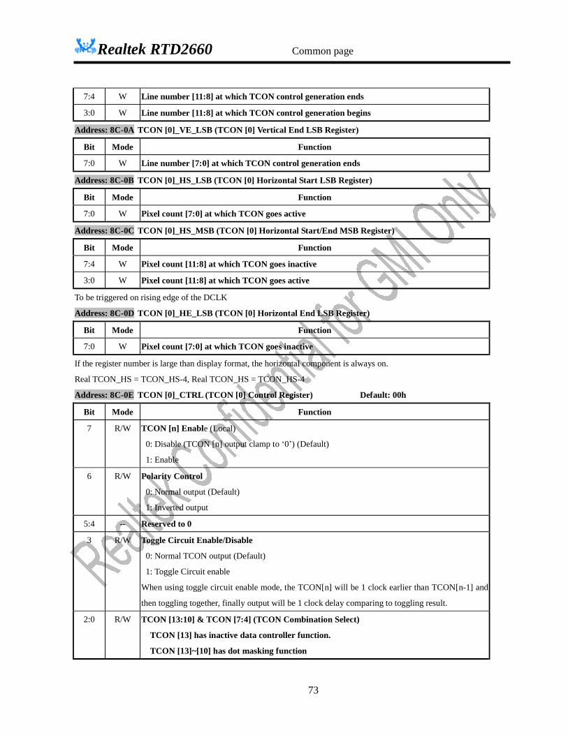
Realtek RTD2660 Common page
73
7:4 W Line number [11:8] at which TCON control generation ends
3:0 W Line number [11:8] at which TCON control generation begins
Address: 8C-0A TCON [0]_VE_LSB (TCON [0] Vertical End LSB Register)
Bit Mode Function
7:0 W Line number [7:0] at which TCON control generation ends
Address: 8C-0B TCON [0]_HS_LSB (TCON [0] Horizontal Start LSB Register)
Bit Mode Function
7:0 W Pixel count [7:0] at which TCON goes active
Address: 8C-0C TCON [0]_HS_MSB (TCON [0] Horizontal Start/End MSB Register)
Bit Mode Function
7:4 W Pixel count [11:8] at which TCON goes inactive
3:0 W Pixel count [11:8] at which TCON goes active
To be triggered on rising edge of the DCLK
Address: 8C-0D TCON [0]_HE_LSB (TCON [0] Horizontal End LSB Register)
Bit Mode Function
7:0 W Pixel count [7:0] at which TCON goes inactive
If the register number is large than display format, the horizontal component is always on.
Real TCON_HS = TCON_HS-4, Real TCON_HS = TCON_HS-4
Address: 8C-0E TCON [0]_CTRL (TCON [0] Control Register) Default: 00h
Bit Mode Function
7 R/W TCON [n] Enable (Local)
0: Disable (TCON [n] output clamp to ‘0’) (Default)
1: Enable
6 R/W Polarity Control
0: Normal output (Default)
1: Inverted output
5:4 -- Reserved to 0
3 R/W Toggle Circuit Enable/Disable
0: Normal TCON output (Default)
1: Toggle Circuit enable
When using toggle circuit enable mode, the TCON[n] will be 1 clock earlier than TCON[n-1] and
then toggling together, finally output will be 1 clock delay comparing to toggling result.
2:0 R/W TCON [13:10] & TCON [7:4] (TCON Combination Select)
TCON [13] has inactive data controller function.
TCON [13]~[10] has dot masking function

Realtek RTD2660 Common page
74
TCON [7] has flicking reduce function.
000: Normal TCON output (Default)
001: Select TCON [n] “AND” with TCON [n-1]
010: Select TCON [n] “OR” with TCON [n-1]
011: Select TCON [n] “XOR” with TCON [n-1]
100: Select TCON [n-1] rising edge as toggle trigger signal (when toggle enable)
101: Select TCON [n-1] rising edge as toggle trigger signal, then “AND” (when toggle enable)
110: Select TCON [n-1] rising edge as toggle trigger signal, then “OR” (when toggle enable)
111: Select TCON [n] and TCON [n-1] on alternating frames.
--------------------------------------------------------------------------------------------------------------------
TCON [9:8] (TCON Combination Select)
000: Normal TCON output
001: Select TCON [n] “AND” with TCON [n-1]
010: Select TCON [n] “OR” with TCON [n-1]
011: Select TCON [n] “XOR” with TCON [n-1]
100: Select TCON [n-1] rising edge as toggle trigger signal (when toggle enable)
101: Select TCON [n-1] rising edge as toggle trigger signal, then “AND” (when toggle enable)
110: Select TCON [n-1] rising edge as toggle trigger signal, then “OR” (when toggle enable)
111: Select TCON [n] and TCON [n-1] reference ODD signal as alternating frames.
--------------------------------------------------------------------------------------------------------------------
TCON [3] (TCON Combination Select)
000: Normal TCON output
001: Select TCON [3] “AND” with TCON [2]
010: Select TCON [3] “OR” with TCON [2]
011: Select TCON [3] “XOR” with TCON [2]
100: Select TCON [2] rising edge as toggle trigger signal (when toggle enable)
101: Select TCON [2] rising edge as toggle trigger signal, then “AND” (when toggle enable)
110: Select TCON [2] rising edge as toggle trigger signal, then “OR” (when toggle enable)
111: Select reset(ODD=0) or set(ODD=1) TCON [3] by DVS, when toggle function enable
--------------------------------------------------------------------------------------------------------------------
TCON [2] (Clock Toggle Function)//toggle function is inactive
00x: Normal TCON output
010: Select DCLK/2 when TCON [2] is “0”
011: Select DCLK/2 when TCON [2] is “1”
100: Select DCLK/4 when TCON [2] is “0”
101: Select DCLK/4 when TCON [2] is “1”
110: Select DCLK/8 when TCON [2] is “0”
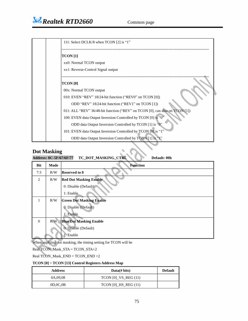
Realtek RTD2660 Common page
75
111: Select DCLK/8 when TCON [2] is “1”
--------------------------------------------------------------------------------------------------------------------
TCON [1]
xx0: Normal TCON output
xx1: Reverse-Control Signal output
--------------------------------------------------------------------------------------------------------------------
TCON [0]
00x: Normal TCON output
010: EVEN “REV” 18/24-bit function (“REV0” on TCON [0])
ODD “REV” 18/24-bit function (“REV1” on TCON [1])
011: ALL “REV” 36/48-bit function (“REV” on TCON [0], can also on TCON [1])
100: EVEN data Output Inversion Controlled by TCON [0] is “0”
ODD data Output Inversion Controlled by TCON [1] is “0”
101: EVEN data Output Inversion Controlled by TCON [0] is “1”
ODD data Output Inversion Controlled by TCON [1] is “1”
Dot Masking Address: 8C-5F/67/6F/77 TC_DOT_MASKING_CTRL Default: 00h
Bit Mode Function
7:3 R/W Reserved to 0
2 R/W Red Dot Masking Enable
0: Disable (Default)
1: Enable
1 R/W Green Dot Masking Enable
0: Disable (Default)
1: Enable
0 R/W Blue Dot Masking Enable
0: Disable (Default)
1: Enable
When applying dot masking, the timing setting for TCON will be
Real TCON_Mask_STA = TCON_STA+2
Real TCON_Mask_END = TCON_END +2
TCON [0] ~ TCON [13] Control Registers Address Map
Address Data(# bits) Default
0A,09,08 TCON [0]_VS_REG (11)
0D,0C,0B TCON [0]_HS_REG (11)

Realtek RTD2660 Common page
76
0E TCON [0]_CTRL_REG 00
0F Reserved
12,11,10 TCON [1]_VS_REG (11)
15,14,13 TCON [1]_HS_REG (11)
16 TCON [1]_CTRL_REG 00
17 Reserved
1A,19,18 TCON [2]_VS_REG (11)
1D,1C,1B TCON [2]_HS_REG (11)
1E TCON [2]_CTRL_REG 00
1F Reserved
22,21,20 TCON [3]_VS_REG (11)
25,24,23 TCON [3]_HS_REG (11)
26 TCON [3]_CTRL_REG 00
27 Reserved
2A,29,28 TCON [4]_VS_REG (11)
2D,2C,2B TCON [4]_HS_REG (11)
2E TCON [4]_CTRL_REG 00
2F Reserved
32,31,30 TCON [5]_VS_REG (11)
35,34,33 TCON [5]_HS_REG (11)
36 TCON [5]_CTRL_REG 00
37 Reserved
3A,39,38 TCON [6]_VS_REG (11)
3D,3C,3B TCON [6]_HS_REG (11)
3E TCON [6]_CTRL_REG 00
3F Reserved
42,41,40 TCON [7]_VS_REG (11)
45,44,43 TCON [7]_HS_REG (11)

Realtek RTD2660 Common page
77
46 TCON [7]_CTRL_REG 00
47 Reserved
4A,49,48 TCON [8]_VS_REG (11)
4D,4C,4B TCON [8]_HS_REG (11)
4E TCON [8]_CTRL_REG 00
4F Reserved
52,51,50 TCON [9]_VS_REG (11)
55,54,53 TCON [9]_HS_REG (11)
56 TCON [9]_CTRL_REG 00
57 Reserved
5A,59,58 TCON [10]_VS_REG (11)
5D,5C,5B TCON [10]_HS_REG (11)
5E TCON [10]_CTRL_REG 00
5F TCON [10]_CTRL_REG
62,61,60 TCON [11]_VS_REG (11)
65,64,63 TCON [11]_HS_REG (11)
66 TCON [11]_CTRL_REG 00
67 TCON [11]_CTRL_REG 00
6A,69,68 TCON [12]_VS_REG (11)
6D,6C,6B TCON [12]_HS_REG (11)
6E TCON [12]_CTRL_REG 00
6F TCON [12]_CTRL_REG 00
72,71,70 TCON [13]_VS_REG (11)
75,74,73 TCON [13]_HS_REG (11)
76 TCON [13]_CTRL_REG 00
77 TCON [13]_CTRL_REG 00

Realtek RTD2660 Common page
78
Control for LVDS Address: 8C-A0 LVDS_CTRL0 Default: 00h
Bit Mode Function 7:6 -- Reserved to 0 5 R/W Power Up LVDS Even-Port
0: Power down (Default)
1: Normal 4 R/W Power Up LVDS Odd-Port
0: Power down (Default)
1: Normal 3:2 R/W Watch Dog Model
00: Enable Watch Dog(Default)
01: Keep PLL VCO = 1V
1x: Disable Watch Dog
1 R/W ENVBPBL: Enable VCO_D2S Current Up
0: disable (Default)
1: enable 0 R Watch Dog Control Flag
0: Watch dog not active (Default)
1: Watch dog active, Reset PLL and set VCO = 1V
Address: 8C-A1 LVDS_CTRL1 Default: 14h Bit Mode Function 7 R/W BCKPOLARL: Inverse the CK7X
0: no inverse
1: inverse 6 R/W DCKPOLARL: Inverse the CK7X
0: no inverse
1: inverse 5:3 R/W STSTL [2:0]: select test attribute
000: WD
001: VCOM
010: IB40u (default)
011: IBVOCM
100: PLLTST-fbak
101: PLLTST-fin
110: LVTST-CKDIN
111: LVTST-LVDSIN[6]

Realtek RTD2660 Common page
79
2:0 R/W RSDS / LVDS Output Common Mode (Default: 100)
Address: 8C-A2 LVDS_CTRL2 Default: 43h Bit Mode Function 7:6 R/W SBGL
00: 1.14V
01: 1.20V (Default)
10: 1.27V
11: 1.33V
5 R/W ENIB40UX2L: Double the LVDS/RSDS output swing
0: 1X
1: 2X 4 R/W SIBXL : select 20uA source
0: from Bandgap (Default) 1: from ADC
3 R/W PLL lock edge
0: positive
1: negative 2:0 R/W Bias Generator Adjust (011)
Address: 8C-A3 LVDS_CTRL3 Default: 1Ch
Bit Mode Function
7 R/W LVDS Differential pair PN swap (data) (Also refer to CR29[6:4])
0: No Swap (Default)
1: Swap
6 R/W LVDS Mirror
0: Normal (TXE3+, TXE3-, TXEC+, TXEC-, TXE2+, TXE2-, TXE1+, TXE1-, TXE0+, TXE0-,
TXO3+, TXO3-, TXOC+, TXOC-, TXO2+, TXO2-, TXO1+, TXO1-, TXO0+, TXO0-)
1: Mirror (TXE0-, TXE0+, TXE1-, TXE1+, TXE2-, TXE2+, TXEC-, TXEC+, TXE3-, TXE3+,
TXO0-, TXO0+, TXO1-, TXO1+, TXO2-, TXO2+, TXOC-, TXOC+, TXO3-, TXO3+) 5:3 R/W SIL [2:0]: PLL charge pump current (I=5uA+5uA*code) (Default: 011) 2:1 R/W SRL [1:0]: PLL resistor (R=6K+2K*code) (Default: 10) 0 R/W BMTS: Bit-Mapping Table Select
0: Table 1 (Default)
1: Table 2
Address: 8C-A4 LVDS_CTRL4 Default: 80h Bit Mode Function 7:6 R/W E_RSV: even port reserve signal select
11: Always ‘1’
10: Always ‘0’
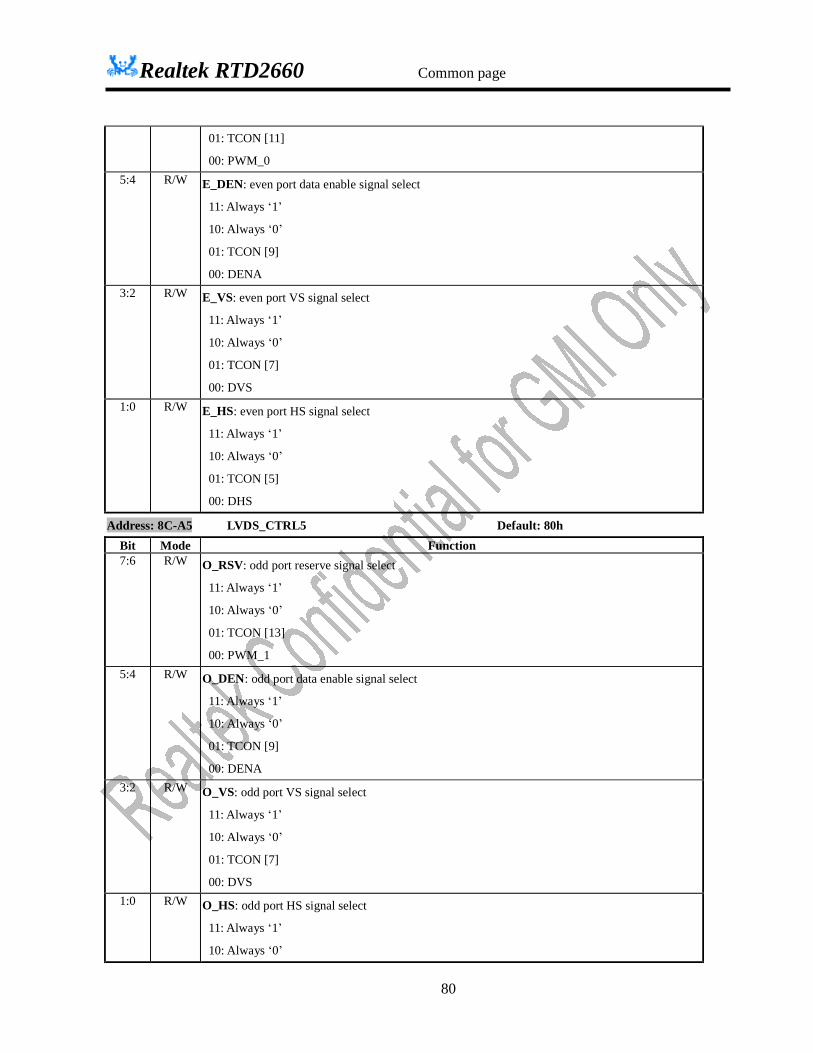
Realtek RTD2660 Common page
80
01: TCON [11]
00: PWM_0 5:4 R/W E_DEN: even port data enable signal select
11: Always ‘1’
10: Always ‘0’
01: TCON [9]
00: DENA 3:2 R/W E_VS: even port VS signal select
11: Always ‘1’
10: Always ‘0’
01: TCON [7]
00: DVS 1:0 R/W E_HS: even port HS signal select
11: Always ‘1’
10: Always ‘0’
01: TCON [5]
00: DHS
Address: 8C-A5 LVDS_CTRL5 Default: 80h Bit Mode Function 7:6 R/W O_RSV: odd port reserve signal select
11: Always ‘1’
10: Always ‘0’
01: TCON [13]
00: PWM_1 5:4 R/W O_DEN: odd port data enable signal select
11: Always ‘1’
10: Always ‘0’
01: TCON [9]
00: DENA 3:2 R/W O_VS: odd port VS signal select
11: Always ‘1’
10: Always ‘0’
01: TCON [7]
00: DVS 1:0 R/W O_HS: odd port HS signal select
11: Always ‘1’
10: Always ‘0’

Realtek RTD2660 Common page
81
01: TCON [5]
00: DHS
Embedded OSD Address: 90 OSD_ADDR_MSB (OSD Address MSB 8-bit)
Bit Mode Function
7:0 R/W OSD MSB 8-bit address
Address: 91 OSD _ADDR_LSB (OSD Address LSB 8-bit)
Bit Mode Function
7:0 R/W OSD LSB 8-bit address
Address: 92 OSD_DATA_PORT (OSD Data Port)
Bit Mode Function
7:0 W Data port for embedded OSD access
Refer to the embedded OSD application note for the detailed.
Address: 93 OSD_SCRAMBLE Default: 05h
Bit Mode Function
7 R/W BIST Start
0: stop (Default)
1: start (auto clear)
6 R BIST Result
0: fail (Default)
1: success
5 R MCU writes data when OSD ON status (Queue 1 byte data)
0: MCU writes data to OSD but not to real position (There is one level buffer here)
1: MCU doesn’t write data, or data has been written to real position
4 R Double_Buffer_Write_Status
0: double buffer write out is finish, or data write to double buffer is not ready, or no double buffer
function.
1: after data write to dbuf and before dbuf write out, such that double buffer is busy.
3 R/W OSDADRHSB
0: If initial address lower than or equal to 12K
1: If initial address higher than 12K
The bit will be designed to control 16.5K bytes SRAM. However it will have no effect for
WINDOW setting. Also please remember to set {OSDADRHSB, OSDADRMSB(CR90),
OSDADRLSB(CR91) } again while you like to R/W a new address.
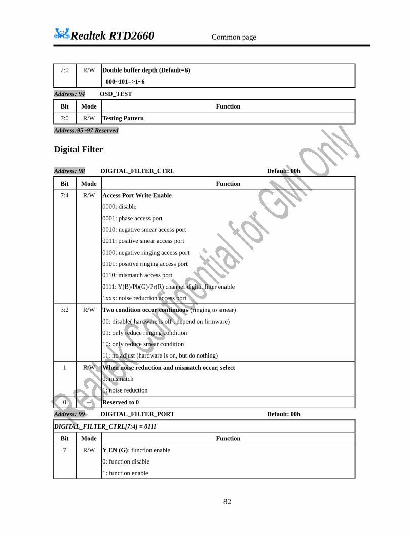
Realtek RTD2660 Common page
82
2:0 R/W Double buffer depth (Default=6)
000~101=>1~6
Address: 94 OSD_TEST
Bit Mode Function
7:0 R/W Testing Pattern
Address:95~97 Reserved Digital Filter
Address: 98 DIGITAL_FILTER_CTRL Default: 00h
Bit Mode Function
7:4 R/W Access Port Write Enable
0000: disable
0001: phase access port
0010: negative smear access port
0011: positive smear access port
0100: negative ringing access port
0101: positive ringing access port
0110: mismatch access port
0111: Y(B)/Pb(G)/Pr(R) channel digital filter enable
1xxx: noise reduction access port
3:2 R/W Two condition occur continuous (ringing to smear)
00: disable( hardware is off , depend on firmware)
01: only reduce ringing condition
10: only reduce smear condition
11: no adjust (hardware is on, but do nothing)
1 R/W When noise reduction and mismatch occur, select
0: mismatch
1: noise reduction
0 -- Reserved to 0
Address: 99 DIGITAL_FILTER_PORT Default: 00h
DIGITAL_FILTER_CTRL[7:4] = 0111
Bit Mode Function
7 R/W Y EN (G): function enable
0: function disable
1: function enable
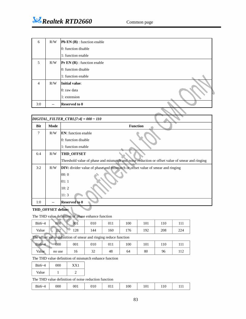
Realtek RTD2660 Common page
83
6 R/W Pb EN (B) : function enable
0: function disable
1: function enable
5 R/W Pr EN (R) : function enable
0: function disable
1: function enable
4 R/W Initial value:
0: raw data
1: extension
3:0 -- Reserved to 0
DIGITAL_FILTER_CTRL[7:4] = 000 ~ 110
Bit Mode Function
7 R/W EN: function enable
0: function disable
1: function enable
6:4 R/W THD_OFFSET
Threshold value of phase and mismatch and noise reduction or offset value of smear and ringing
3:2 R/W DIV: divider value of phase and mismatch or offset value of smear and ringing
00: 0
01: 1
10: 2
11: 3
1:0 -- Reserved to 0
THD_OFFSET define:
The THD value definition of phase enhance function
Bit6~4 000 001 010 011 100 101 110 111
Value 112 128 144 160 176 192 208 224
The offset value definition of smear and ringing reduce function
Bit6~4 000 001 010 011 100 101 110 111
Value no use 16 32 48 64 80 96 112
The THD value definition of mismatch enhance function
Bit6~4 000 XX1
Value 1 2
The THD value definition of noise reduction function
Bit6~4 000 001 010 011 100 101 110 111
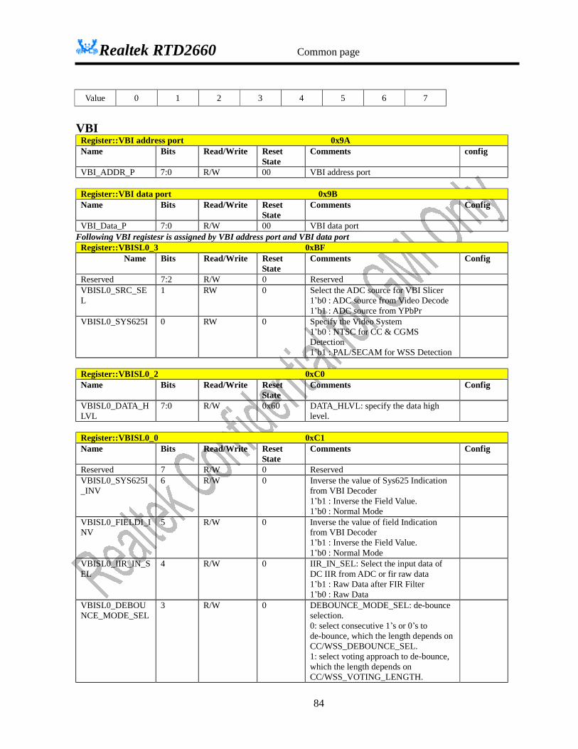
Realtek RTD2660 Common page
84
Value 0 1 2 3 4 5 6 7
VBI
Register::VBI address port 0x9A Name Bits Read/Write Reset
State Comments config
VBI_ADDR_P 7:0 R/W 00 VBI address port
Register::VBI data port 0x9B Name Bits Read/Write Reset
State Comments Config
VBI_Data_P 7:0 R/W 00 VBI data port Following VBI registesr is assigned by VBI address port and VBI data port
Register::VBISL0_3 0xBF Name Bits Read/Write Reset
State Comments Config
Reserved 7:2 R/W 0 Reserved VBISL0_SRC_SEL
1 RW 0 Select the ADC source for VBI Slicer 1’b0 : ADC source from Video Decode 1’b1 : ADC source from YPbPr
VBISL0_SYS625I 0 RW 0 Specify the Video System 1’b0 : NTSC for CC & CGMS Detection 1’b1 : PAL/SECAM for WSS Detection
Register::VBISL0_2 0xC0 Name Bits Read/Write Reset
State Comments Config
VBISL0_DATA_HLVL
7:0 R/W 0x60 DATA_HLVL: specify the data high level.
Register::VBISL0_0 0xC1 Name Bits Read/Write Reset
State Comments Config
Reserved 7 R/W 0 Reserved VBISL0_SYS625I_INV
6 R/W 0 Inverse the value of Sys625 Indication from VBI Decoder 1’b1 : Inverse the Field Value. 1’b0 : Normal Mode
VBISL0_FIELDI_INV
5 R/W 0 Inverse the value of field Indication from VBI Decoder 1’b1 : Inverse the Field Value. 1’b0 : Normal Mode
VBISL0_IIR_IN_SEL
4 R/W 0 IIR_IN_SEL: Select the input data of DC IIR from ADC or fir raw data 1’b1 : Raw Data after FIR Filter 1’b0 : Raw Data
VBISL0_DEBOUNCE_MODE_SEL
3 R/W 0 DEBOUNCE_MODE_SEL: de-bounce selection. 0: select consecutive 1’s or 0’s to de-bounce, which the length depends on CC/WSS_DEBOUNCE_SEL. 1: select voting approach to de-bounce, which the length depends on CC/WSS_VOTING_LENGTH.
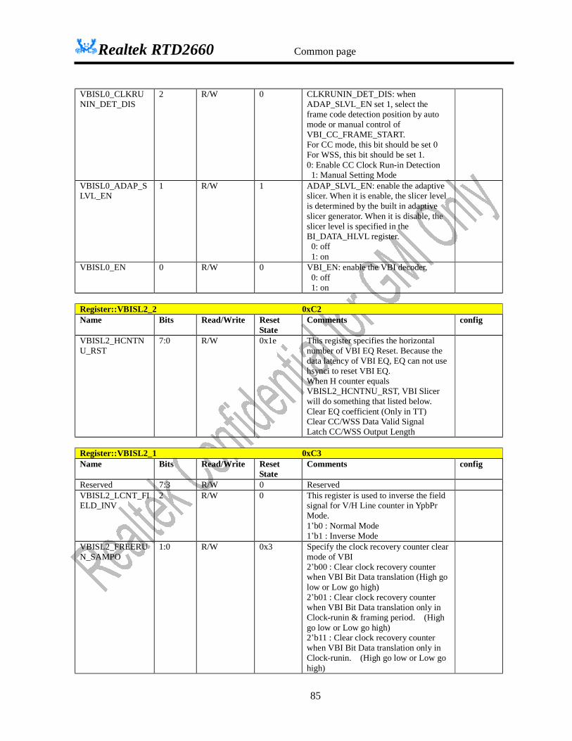
Realtek RTD2660 Common page
85
VBISL0_CLKRUNIN_DET_DIS
2 R/W 0 CLKRUNIN_DET_DIS: when ADAP_SLVL_EN set 1, select the frame code detection position by auto mode or manual control of VBI_CC_FRAME_START. For CC mode, this bit should be set 0 For WSS, this bit should be set 1. 0: Enable CC Clock Run-in Detection 1: Manual Setting Mode
VBISL0_ADAP_SLVL_EN
1 R/W 1 ADAP_SLVL_EN: enable the adaptive slicer. When it is enable, the slicer level is determined by the built in adaptive slicer generator. When it is disable, the slicer level is specified in the BI_DATA_HLVL register. 0: off 1: on
VBISL0_EN 0 R/W 0 VBI_EN: enable the VBI decoder. 0: off 1: on
Register::VBISL2_2 0xC2 Name Bits Read/Write Reset
State Comments config
VBISL2_HCNTNU_RST
7:0 R/W 0x1e This register specifies the horizontal number of VBI EQ Reset. Because the data latency of VBI EQ, EQ can not use hsynci to reset VBI EQ. When H counter equals VBISL2_HCNTNU_RST, VBI Slicer will do something that listed below. Clear EQ coefficient (Only in TT) Clear CC/WSS Data Valid Signal Latch CC/WSS Output Length
Register::VBISL2_1 0xC3 Name Bits Read/Write Reset
State Comments config
Reserved 7:3 R/W 0 Reserved VBISL2_LCNT_FIELD_INV
2 R/W 0 This register is used to inverse the field signal for V/H Line counter in YpbPr Mode. 1’b0 : Normal Mode 1’b1 : Inverse Mode
VBISL2_FREERUN_SAMPO
1:0 R/W 0x3 Specify the clock recovery counter clear mode of VBI 2’b00 : Clear clock recovery counter when VBI Bit Data translation (High go low or Low go high) 2’b01 : Clear clock recovery counter when VBI Bit Data translation only in Clock-runin & framing period. (High go low or Low go high) 2’b11 : Clear clock recovery counter when VBI Bit Data translation only in Clock-runin. (High go low or Low go high)

Realtek RTD2660 Common page
86
Register::VBISL2_0 0xC4 Name Bits Read/Write Reset
State Comments config
VBISL2_MCFG_B 7:4 R/W 0x1 .Specify the VBI mode of active line of Bottom Field to detect. CC & WSS does not exist in active line simultaneously. 4’h1 : CC Mode 4’hC: WSS Mode Others : Disable VBI Detection Mode
VBISL2_MCFG_T 3:0 R/W 0x1 .Specify the VBI mode of active line of Top Field to detect. CC & WSS does not exist in active line simultaneously. 4’h1 : CC Detection Mode 4’hC: WSS Detection Mode Others : Disable VBI Detection Mode
Register::VBISL3_3 0xC5 Name Bits Read/Write Reset
State Comments config
Reserved 7:2 R/W 0 Reserved VBISL3_ALINE_B_MSB
1:0 R/W 0x1 Specify the active line of Bottom Field to detect CC or WSS. CC & WSS does not exist in active line simultaneously. Normally : CC exists in line 21 & 284. WSS exist in line 23 Line Number Include Line offset. For NTSC system, line offset is 6. For PAL/SECAM system, line offset is 3.
Register::VBISL3_2 0xC6 Name Bits Read/Write Reset
State Comments config
VBISL3_ALINE_B_LSB
7:0 R/W 0x16 Specify the active line of Bottom Field to detect CC or WSS. CC & WSS does not exist in active line simultaneously. Normally : CC exists in line 21 & 284. WSS exist in line 23 Line Number Include Line offset. For NTSC system, line offset is 6. For PAL/SECAM system, line offset is 3.
Register::VBISL3_1 0xC7 Name Bits Read/Write Reset
State Comments config
Reserved 7:2 R/W 0 Reserved VBISL3_ALINE_T_MSB
1:0 R/W 0 Specify the active line of Top Field to detect CC or WSS. CC & WSS does not exist in active line simultaneously. Normally : CC exists in line 21 & 284. WSS exist in line 23 Line Number Include Line offset. For NTSC system, line offset is 6. For PAL/SECAM system, line offset is 3.

Realtek RTD2660 Common page
87
Register::VBISL3_0 0xC8 Name Bits Read/Write Reset
State Comments config
VBISL3_ALINE_T_LSB
7:0 R/W 0x0f Specify the active line of Top Field to detect CC or WSS. CC & WSS does not exist in active line simultaneously. Normally : CC exists in line 21 & 284. WSS exist in line 23 Line Number Include Line offset. For NTSC system, line offset is 6. For PAL/SECAM system, line offset is 3.
Register::VBISL6_3 0xC9 Name Bits Read/Write Reset
State Comments config
VBISL7_WSS625_DTO_MSB
7:0 R/W 0x15 WSS625_DTO: the 16-bit DTO incremental value for wss625 clock recovery circuit.
Register::VBISL6_2 0xCA Name Bits Read/Write Reset
State Comments config
VBISL7_WSS625_DTO_LSB
7:0 R/W 0x9a WSS625_DTO: the 16-bit DTO incremental value for wss625 clock recovery circuit.
Register::VBISL6_1 0xCB Name Bits Read/Write Reset
State Comments config
VBISL6_CAPTION_DTO_MSB
7:0 R/W 0x35 CAPTION_DTO: the 16-bit DTO incrementer value for close caption clock recovery circuit.
Register::VBISL6_0 0xCC Name Bits Read/Write Reset
State Comments config
VBISL6_CAPTION_DTO_LSB
7:0 R/W 0x9F CAPTION_DTO: the 16-bit DTO incrementer value for close caption clock recovery circuit.
Register::VBISL8_3 0xCD Name Bits Read/Write Reset
State Comments config
VBISL9_WSS_FRAME_START
7:0 R/W 0x64 WSS625_FRAME_START: The value of pixel count for VBI Slicer start to detect the framing code of WSS.
Register::VBISL8_2 0xCE Name Bits Read/Write Reset
State Comments config
VBISL9_CC_FRAME_START
7:0 R/W 0x64 CC_FRAME_START: The value of pixel count for VBI Slicer start to detect the framing code of closed caption.

Realtek RTD2660 Common page
88
Register::VBISL8_1 0xCF Name Bits Read/Write Reset
State Comments config
VBISL8_WSS_START
7:0 R/W 0x5a WSS625_START: The value of pixel count for VBI Slicer start to detect the framing code of WSS.
Register::VBISL8_0 0xD0 Name Bits Read/Write Reset
State Comments config
VBISL8_CC_START
7:0 R/W 0x5a CC_START: The value of pixel count for VBI Slicer start to detect the framing code of closed caption.
Register::VBISL10_2 0xD1 Name Bits Read/Write Reset
State Comments config
VBISL10_CC_PERIOD_MIN_CYC
7:0 R/W 0x20 CC_PERIOD_MIN_CYC: If the period counter of per clock run-in of teletext is in the range between CC_PERIOD_MAX_CYC and CC_PERIOD_MIN_CYC, the valid clock run-in counter of received teletext add 1.
Register::VBISL10_1 0xD2 Name Bits Read/Write Reset
State Comments config
VBISL10_CC_PERIOD_MAX_CYC
7:0 R/W 0x44 CC_PERIOD_MAX_CYC: If the period counter of per clock run-in of teletext is in the range between CC_PERIOD_MAX_CYC and CC_PERIOD_MIN_CYC, the valid clock run-in counter of received teletext add 1.
Register::VBISL10_0 0xD3 Name Bits Read/Write Reset
State Comments config
VBISL10_CC_VOTING_SEL
7:6 R/W 0 CC_VOTING_SEL: length choice for cc voting decision. 00: 3 01: 5 10: 7 11: 9
VBISL10_CC_DC_FIR_SEL
5:4 R/W 0x3 CC_DC_FIR_SEL: Selection FIR Mode for CC DC Detection 2’b00: 2 points average of FIR. 2’b01: 4 points average of FIR. 2’b10: 8 points average of FIR. 2’b11: 16 points average of FIR others: 4 points average of FIR.
VBISL10_CC_DC_IIR_SEL
3:2 R/W 0x2 CC_DC_IIR_SEL: Selection IIR Mode for CC DC Detection (b/(1-axZ[-1])) 2’b00: a = 3/4;

Realtek RTD2660 Common page
89
2’b01: a = 7/8; 2’b10: a = 15/16; 2’b11: a = 31/32; others: a = 7/8;
VBISL10_CC_RAW_FIR_SEL
1:0 R/W 0x2 CC_RAW_FIR_SEL: Selection the FIR Mode Selection for VBI Raw Data. 2’b00: 2 points average of FIR. 2’b01: 4 points average of FIR. 2’b10: 8 points average of FIR. others: 2 points average of FIR.for VBI Slicer start to detect the framing code of closed caption.
Register::VBISL11_2 0xD4 Name Bits Read/Write Reset
State Comments config
Reserved 7:5 R/W 0 Reserved VBISL11_CC_FIRST_BIT_CYC
4:0 R/W 0x1f CC_FIRST_BIT_CYC : The First Bit Cycle of CC. After latching correct DC value of CC, VBI Slicer start to count the cycles of “0” bits. If the cycle number of bit cycu counter above CC_FIRST_BIT_CYC, and VBI Slicer start to detect framing code.
Register::VBISL11_1 0xD5 Name Bits Read/Write Reset
State Comments config
Reserved 7:3 R/W 0 Reserved VBISL11_CC_DEBOUNCE_SEL
2:0 R/W 0x7 CC_DEBOUNCE_SEL: Select the mode of debounce mechanism of Teletext Data. 3’h0: No De-bounce, ’0’ => 0 ;’1’ => 1; 3’h1: De-bounce 2T. ‘00’ => 0 ; ‘11’=> 1; 3’h2: De-bounce 3T, ‘000’ => 0 ; ‘111’ => 1; 3’h3: De-bounce 4T, ‘0000’ => 0; ‘1111’ => 1; 3’h7: De-bounce 8T, ‘0000_0000’=>0; ‘1111_1111’=>1;
Register::VBISL11_0 0xD6 Name Bits Read/Write Reset
State Comments config
Reserved 7:4 R/W 0 Reserved VBISL11_CC_VALID_CLKRUNIN_NU
3:0 R/W 0x3 CC_VALID_CLKRUNIN_NU: The valid continuing clock run-in counter of teletext is larger or equal to CC_VALID_CLKRUNIN_NU, VBI Slicer start to calculate the DC value of teletext.
Register::VBISL14_1 0xD7 Name Bits Read/Write Reset
State Comments config
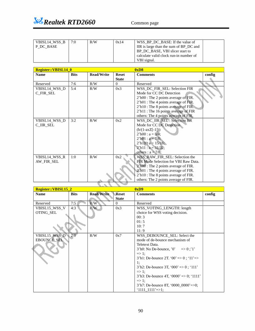
Realtek RTD2660 Common page
90
VBISL14_WSS_BP_DC_BASE
7:0 R/W 0x14 WSS_BP_DC_BASE: If the value of IIR is large than the sum of BP_DC and BP_DC_BASE, VBI slicer start to calculate valid clock run-in number of VBI signal.
Register::VBISL14_0 0xD8 Name Bits Read/Write Reset
State Comments config
Reserved 7:6 R/W 0 Reserved VBISL14_WSS_DC_FIR_SEL
5:4 R/W 0x3 WSS_DC_FIR_SEL: Selection FIR Mode for CC DC Detection 2’b00 : The 2 points average of FIR. 2’b01 : The 4 points average of FIR. 2’b10 : The 8 points average of FIR. 2’b11 : The 16 points average of FIR others: The 4 points average of FIR.
VBISL14_WSS_DC_IIR_SEL
3:2 R/W 0x2 WSS_DC_IIR_SEL : Selection IIR Mode for CC DC Detection (b/(1-axZ[-1])) 2’b00 : a = 3/4; 2’b01 : a = 7/8; 2’b10 : a = 15/16; 2’b11 : a = 31/32; others : a = 7/8;
VBISL14_WSS_RAW_FIR_SEL
1:0 R/W 0x2 WSS_RAW_FIR_SEL: Selection the FIR Mode Selection for VBI Raw Data. 2’b00 : The 2 points average of FIR. 2’b01 : The 4 points average of FIR. 2’b10 : The 8 points average of FIR. others: The 2 points average of FIR.
Register::VBISL15_2 0xD9 Name Bits Read/Write Reset
State Comments config
Reserved 7:5 R/W 0 Reserved VBISL15_WSS_VOTING_SEL
4:3 R/W 0x3 WSS_VOTING_LENGTH: length choice for WSS voting decision. 00: 3 01: 5 10: 7 11: 9
VBISL15_WSS_DEBOUNCE_SEL
2:0 R/W 0x7 WSS_DEBOUNCE_SEL: Select the mode of de-bounce mechanism of Teletext Data. 3’h0: No De-bounce, ’0’ => 0 ;’1’ => 1; 3’h1: De-bounce 2T. ‘00’ => 0 ; ‘11’=> 1; 3’h2: De-bounce 3T, ‘000’ => 0 ; ‘111’ => 1; 3’h3: De-bounce 4T, ‘0000’ => 0; ‘1111’ => 1; 3’h7: De-bounce 8T, ‘0000_0000’=>0; ‘1111_1111’=>1;

Realtek RTD2660 Common page
91
Register::VBISL15_1 0xDA Name Bits Read/Write Reset
State Comments config
VBISL15_WSS_STABLE_DC_NU
7:0 R/W 0x14 WSS_STABLE_DC_NU: The stable dc counter of teletext is larger or equal to WSS_STABLE_DC_NU, VBI Slicer start to calculate the DC value of teletext.
Register::VBISL15_0 0xDB Name Bits Read/Write Reset
State Comments config
VBISL15_WSS_STABLE_DC_LOW_THD
7:0 R/W 0x2 WSS_STABLE_LOW_THD: The low threshold of stable dc detection.
Register::VBISL16_0 0xDC Name Bits Read/Write Reset
State Comments config
Reserved 7:3 R/W 0 Reserved VBISL16_CGMS_INT_EN
2 R/W 0 Enable the interrupt function of CGMS 1’b1 : Enable. 1’b0 : Disable.
VBISL16_WSS_INT_EN
1 R/W 0 Enable the interrupt function of WSS 1’b1 : Enable. 1’b0 : Disable.
VBISL16_CC_INT_EN
0 R/W 0 Enable the interrupt function of CC 1’b1 : Enable. 1’b0 : Disable.
Register::VBISL161_1 0xDD Name Bits Read/Write Reset
State Comments config
VBISL16_CC_RUNIN_PERIOD
7:0 R 0 Latch the clock runin period when Clock run-in is valid
Register::VBISL161_0 0xDE Name Bits Read/Write Reset
State Comments config
Reserved 7 R/W 0 Reserved CGMS_C4_CGMS_VLD_CLR
6 R/W 0 Write “1” to clear CGMS_C4_CGMS_VLD
VBISL16_WSS_RDY_CLR
5 R/W 0 Write “1” to clear BISL16_WSS_RDY
VBISL16_CC_RDY_CLR
4 R/W 0 Write “1” to clear VBISL16_CC_RDY
CGMS_C4_CGMS_VLD
3 R 0 CGMS DATA_Valid Indicator (Event Mode) 1: Valid. 0: Non-valid.
VBISL16_CC_FIELD
2 R 0 CC Field Indication: 0 : Top Field 1 : Bottom Field

Realtek RTD2660 Common page
92
VBISL16_WSS_RDY
1 R 0 WSS_RDY: The received data ready indicator for WSS. (write “1” to clear)
VBISL16_CC_RDY
0 R 0 CC_RDY: The received data ready indicator for CC. (write “1” to clear)
Register::VBISL17_1 0xDF Name Bits Read/Write Reset
State Comments config
VBISL17_CC_DATA1o
7:0 R 0 CC_DATA1o: The 2th byte of CC.
Register::VBISL17_0 0xE0 Name Bits Read/Write Reset
State Comments config
VBISL17_CC_DATA0o
7:0 R 0 CC_DATA0o: The 1th byte of CC.
Register::VBISL171_1 0xE1 Name Bits Read/Write Reset
State Comments config
VBISL17_WSS_DATA1o
7:0 R 0 WSS_DATA1o: The 2th byte of WSS.
Register::VBISL171_0 0xE2 Name Bits Read/Write Reset
State Comments config
VBISL17_WSS_DATA0o
7:0 R 0 WSS_DATA0o: The 1th byte of WSS.
Register::CGMS_C0_3 0xE3 Name Bits Read/Write Reset
State Comments config
Reserved 7:3 R/W 00 reserved CGMS_C0_DEBOUNCE_SEL
2:0 R/W 0x7 Debounce Mode Selection 3’h0 : No-debounce. 3’h1 : 2T Debounce …. 3’h7: 8T Debounce
Register::CGMS_C0_2 0xE4 Name Bits Read/Write Reset
State Comments config
Reserved 7:2 R/W 0 reserved CGMS_C0_SLICER_DCL_MSB
1:0 R/W 1 Manual Slicer DC level Setting
Register::CGMS_C0_1 0xE5 Name Bits Read/Write Reset
State Comments config
CGMS_C0_SLICER_DCL_LSB
7:0 R/W 00 Manual Slicer DC level Setting
Register::CGMS_C0_0 0xE6 Name Bits Read/Write Reset Comments config
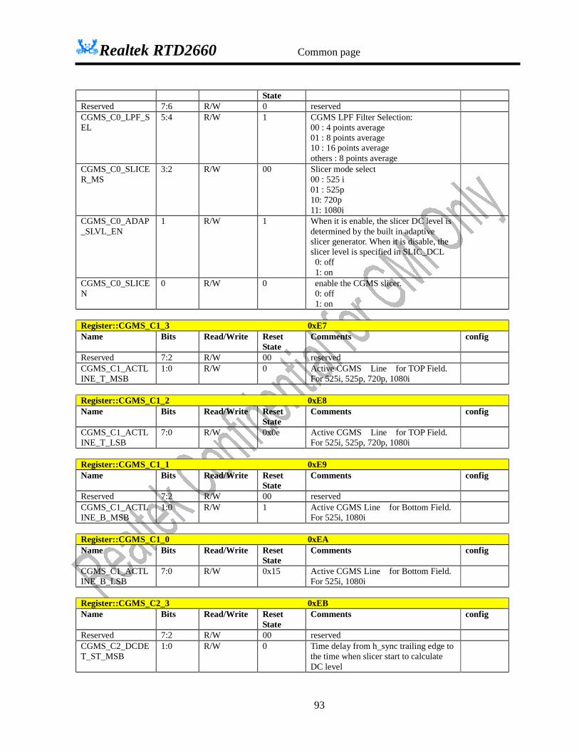
Realtek RTD2660 Common page
93
State Reserved 7:6 R/W 0 reserved CGMS_C0_LPF_SEL
5:4 R/W 1 CGMS LPF Filter Selection: 00 : 4 points average 01 : 8 points average 10 : 16 points average others : 8 points average
CGMS_C0_SLICER_MS
3:2 R/W 00 Slicer mode select 00 : 525 i 01 : 525p 10: 720p 11: 1080i
CGMS_C0_ADAP_SLVL_EN
1 R/W 1 When it is enable, the slicer DC level is determined by the built in adaptive slicer generator. When it is disable, the slicer level is specified in SLIC_DCL 0: off 1: on
CGMS_C0_SLICEN
0 R/W 0 enable the CGMS slicer. 0: off 1: on
Register::CGMS_C1_3 0xE7 Name Bits Read/Write Reset
State Comments config
Reserved 7:2 R/W 00 reserved CGMS_C1_ACTLINE_T_MSB
1:0 R/W 0 Active CGMS Line for TOP Field. For 525i, 525p, 720p, 1080i
Register::CGMS_C1_2 0xE8 Name Bits Read/Write Reset
State Comments config
CGMS_C1_ACTLINE_T_LSB
7:0 R/W 0x0e Active CGMS Line for TOP Field. For 525i, 525p, 720p, 1080i
Register::CGMS_C1_1 0xE9 Name Bits Read/Write Reset
State Comments config
Reserved 7:2 R/W 00 reserved CGMS_C1_ACTLINE_B_MSB
1:0 R/W 1 Active CGMS Line for Bottom Field. For 525i, 1080i
Register::CGMS_C1_0 0xEA Name Bits Read/Write Reset
State Comments config
CGMS_C1_ACTLINE_B_LSB
7:0 R/W 0x15 Active CGMS Line for Bottom Field. For 525i, 1080i
Register::CGMS_C2_3 0xEB Name Bits Read/Write Reset
State Comments config
Reserved 7:2 R/W 00 reserved CGMS_C2_DCDET_ST_MSB
1:0 R/W 0 Time delay from h_sync trailing edge to the time when slicer start to calculate DC level

Realtek RTD2660 Common page
94
Register::CGMS_C2_2 0xEC Name Bits Read/Write Reset
State Comments config
CGMS_C2_DCDET_ST_LSB
7:0 R/W 0x64 Time delay from h_sync trailing edge to the time when slicer start to calculate DC level
Register::CGMS_C2_1 0xED Name Bits Read/Write Reset
State Comments config
Reserved 7:2 R/W 00 reserved CGMS_C2_DCDET_END_MSB
1:0 R/W 1 Time delay from h_sync trailing edge to the time when slicer end to calculate DC level
Register::CGMS_C2_0 0xEE Name Bits Read/Write Reset
State Comments config
CGMS_C2_DCDET_END_LSB
7:0 R/W 0x90 Time delay from h_sync trailing edge to the time when slicer end to calculate DC level
Register::CGMS_C3_1 0xEF Name Bits Read/Write Reset
State Comments config
Reserved 7:2 R/W 00 reserved CGMS_C3_LV_DC_TH_MSB
1:0 R/W 0 The minimum DC difference between high and low level to judage if the CGMS Line is valid
Register::CGMS_C3_0 0xF0 Name Bits Read/Write Reset
State Comments config
CGMS_C3_LV_DC_TH_LSB
7:0 R/W 0x1e The minimum DC difference between high and low level to judage if the CGMS Line is valid
Register::CGMS_C4_2 0xF1 Name Bits Read/Write Reset
State Comments config
Reserved 7:4 R/W 00 reserved CGMS_C4_CGMSDATA_MSB
3:0 R 00 CGMS_DATA_OUT[19:0], The sequence is word0[19:18], word1[17:14],word2[13:6],CRCC[5:0].
Register::CGMS_C4_1 0xF2 Name Bits Read/Write Reset
State Comments config
CGMS_C4_CGMSDATA_LSB1
7:0 R 00 CGMS_DATA_OUT[19:0], The sequence is word0[19:18], word1[17:14],word2[13:6],CRCC[5:0].
Register::CGMS_C4_0 0xF3 Name Bits Read/Write Reset
State Comments config
CGMS_C4_CGMS 7:0 R 00 CGMS_DATA_OUT[19:0],
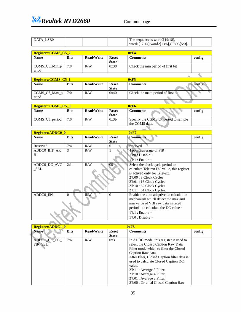
Realtek RTD2660 Common page
95
DATA_LSB0 The sequence is word0[19:18], word1[17:14],word2[13:6],CRCC[5:0].
Register::CGMS_C5_2 0xF4 Name Bits Read/Write Reset
State Comments config
CGMS_C5_Min_period
7:0 R/W 0x38 Check the min period of first bit
Register::CGMS_C5_1 0xF5 Name Bits Read/Write Reset
State Comments config
CGMS_C5_Max_period
7:0 R/W 0x40 Check the mam period of first bit
Register::CGMS_C5_0 0xF6 Name Bits Read/Write Reset
State Comments config
CGMS_C5_period 7:0 R/W 0x3b Specify the CGMS bit period to sample the CGMS data.
Register::ADDC0_0 0xF7 Name Bits Read/Write Reset
State Comments config
Reserved 7:4 R/W 0 reserved ADDC0_BIT_ARB
3 R/W 1 4 points average of FIR 1’b0 : Disable。 1’b1 : Enable。
ADDC0_DC_AVG_SEL
2:1 R/W 00 Select the clock cycle period to calculate Teletext DC value, this register is actived only for Teletext. 2’b00 : 8 Clock Cycles 2’b01 : 16 Clock Cycles 2’b10 : 32 Clock Cycles. 2’b11 : 64 Clock Cycles.
ADDC0_EN 0 R/W 0 Enable the auto adaptive dc calculation mechanism which detect the max and min value of VBI raw data in fixed period to calculate the DC value。 1’b1 : Enable。 1’b0 : Disable。
Register::ADDC1_0 0xF8 Name Bits Read/Write Reset
State Comments config
ADDC1_DC_CC_FIR_SEL
7:6 R/W 0x3 In ADDC mode, this register is used to select the Closed Caption Raw Data Filter mode which to filter the Closed Caption Raw data. After filter, Closed Caption filter data is used to calculate Closed Caption DC value. 2’b11 : Average 8 Filter. 2’b10 : Average 4 Filter. 2’b01 : Average 2 Filter. 2’b00 : Original Closed Caption Raw
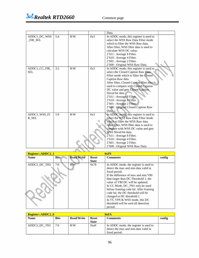
Realtek RTD2660 Common page
96
Data. ADDC1_DC_WSS_FIR_SEL
5:4 R/W 0x3 In ADDC mode, this register is used to select the WSS Raw Data Filter mode which to filter the WSS Raw data. After filter, WSS filter data is used to calculate WSS DC value. 2’b11 : Average 8 Filter. 2’b10 : Average 4 Filter. 2’b01 : Average 2 Filter. 2’b00 : Original WSS Raw Data.
ADDC1_CC_FIR_SEL
3:2 R/W 0x3 In ADDC mode, this register is used to select the Closed Caption Raw Data Filter mode which to filter the Closed Caption Raw data. After filter, Closed Caption fllter data is used to compare with Closed Caption DC value and gets Closed Caption Sliced bit data. 2’b11 : Average 8 Filter. 2’b10 : Average 4 Filter. 2’b01 : Average 2 Filter. 2’b00 : Original Closed Caption Raw Data.
ADDC1_WSS_FIR_SEL
1:0 R/W 0x3 In ADDC mode, this register is used to select the WSS Raw Data Filter mode which to filter the WSS Raw data. After filter, WSS fllter data is used to compare with WSS DC value and gets WSS Sliced bit data. 2’b11 : Average 8 Filter. 2’b10 : Average 4 Filter. 2’b01 : Average 2 Filter. 2’b00 : Original WSS Raw Data.
Register::ADDC2_1 0xF9 Name Bits Read/Write Reset
State Comments config
ADDC2_DC_TH2 7:0 R/W 0x78 In ADDC mode, the register is used to detect the max and min data valid in fixed period. If the difference of max and min VBI date larger than DC Threshold 1, the value of VBI DC will be updated. In CC Mode, DC_TH1 only be used before framing code hit. After framing code hit, the DC threshold will be changed to DC threshold 2. In TT, VPS & WSS mode, this DC threshold will be usrd all detection period.
Register::ADDC2_0 0xFA Name Bits Read/Write Reset
State Comments config
ADDC2_DC_TH1 7:0 R/W 0xa0 In ADDC mode, the register is used to detect the max and min data valid in fixed period.

Realtek RTD2660 Common page
97
If the difference of max and min VBI date larger than DC Threshold 1, the value of VBI DC will be updated. In CC Mode, DC_TH1 only be used before framing code hit. After framing code hit, the DC threshold will be changed to DC threshold 2. In TT, VPS & WSS mode, this DC threshold will be usrd all detection period.
Register::ADDC3_3 0xFB Name Bits Read/Write Reset
State Comments config
Reserved 7:2 R/W 0 reserved REG_ADDC3_MIN_MSB
1:0 R 0 Max value of VBI Data in detection period
Register::ADDC3_2 0xFC Name Bits Read/Write Reset
State Comments config
REG_ADDC3_MIN_LSB
7:0 R 0 Max value of VBI Data in detection period
Register::ADDC3_1 0xFD Name Bits Read/Write Reset
State Comments config
RESERVED 7:2 R/W 0 Reserved REG_ADDC3_MAX_MSB
1:0 R 0 Min value of VBI Data in detection period
Register::ADDC3_0 0xFE Name Bits Read/Write Reset
State Comments config
REG_ADDC3_MAX_LSB
7:0 R 0 Min value of VBI Data in detection period
Address:0xFF Reserved Video Color Space Conversion
Address: 9C YUV_RGB_CTRL (YUV <-> RGB Control Register) Default: 10h
Bit Mode Function
7:5 --- Reserved
4 R/W Color Conversion Type
0: YUV->RGB
1: RGB->YUV (U,V are translated to unsigned 8-bit number)
3 R/W Enable YUV/RGB coefficient Access:
0: Disable
1: Enable
If this bit is set to 0, the address of the data port will reset to 0, and continuously writes 18 bytes

Realtek RTD2660 Common page
98
2 R/W Cb Cr Clamp
0: Bypass
1: Cb-128, Cr-128 (MSB Inversion)
1 R/W Y Gain/Offset:
0 : Bypass
1: (Y-16)*1.164
0 R/W Enable YUV <-> RGB Conversion:
0: Disable YUV<->RGB conversion (Default)
1: Enable YUV<->RGB conversion
Address: 9D YUV_RGB_COEF_DATA
Bit Mode Function
7:0 W COEF_DATA[7:0]
Paged Control Register Address: 9F PAGE_SEL Default: 00h
Bit Mode Function 7:4 R/W Reserved to 0 3:0 R/W Page Selector (CRA0~CRFF)
Page 0: Embedded ADC/ABL/LVR/Smith trigger Page 1: PLL Page 2: Reserved Page 3: Reserved Page 4: Reserved Page 5: Reserved Page 6: Deinterlace/Noise reduction/Scaling down Page 7: vidvid color/DCC/ICM Page 8~PageA: VD Page B:Off line sync processor Page D~PageF:MCU Others: reserved

Realtek RTD2660 Embedded ADC (Page 0)
99
Embedded ADC (Page 0)
Embedded VADC
Register::SOY comparator select 0XA0 Name Bit R/W Default Description Config
ADC_SOYIS1<1:0> 7:6 R/W 00 SOY Comparator1 input select ( OFF
line)
00: VIN0P 01: VIN1P 10: VIN2P 11:
VIN3P
Rev 5:4 --- --- Reserved
ADC_BUFO_SW<1:
0>
3:2 R/W 00 Buffer out switch(A/V out selector)
00: Vin0 to
11: Vin3
REG_ADC_SOY_C
ALI
1 R/W 0 SOG1 ADC&DAC Calibration (0:
Normal 1: Calibration)
Rev 0 --- --- Reserved
Register::ADC CTRL 0XA1
Name Bit R/W Default Description Config
Rev 7 --- --- Reserved
ADC_ADCGC 6 R/W 0 ADC gain calibration(when YPrPb mode)
0: normal 1:calibration
ADC_ADC1_IS 5 R/W 0 ADC1 Video Input Select
0: Video Input1 1: Video Input3
ADC_ADC0_IS 4 R/W 0 ADC0 Video Input Select
0: Video Input10: Video Input2
ADC_IM<3:0> 3:0 R/W F VIN<3:0>N Negative Input Mode
Selection
0: Singel Ended
1: Differential
Register::ADC CLOCK SOURCE 0XA2
Name Bit R/W Default Description Config
Rev 7 --- --- Reserved
ADC_ADC1FTD<2: 6:4 R/W 0 ADC1 input clock fine tune delay

Realtek RTD2660 Embedded ADC (Page 0)
100
0> 000: 0ps to
111: 630ps
Step: 90ps
Rev 3 --- --- Reserved
ADC_ADC0FTD<2:
0>
2:0 R/W 0 ADC0 input clock fine tune delay
000: 0ps to
111: 630ps
Step: 90ps
Register::ADC OUTPUT DELAY CTRL 0XA3
Name Bit R/W Default Description Config
ADC_COD<1:0> 7:6 R/W 0 ADC Clock Output Divider
00:1/1
01:1/2
10:1/3
11:1/4
ADC_ADCOPED<1:
0>
5:4 R/W 0 ADC output pixel extra delay
00:1n
01:1.2n
10:1.4n
11:1.6n
Rev 3 --- --- Reserved
ADC_SOYCLKP 2 R/W 0 SOY1,0_ADC output data polarity
0: positive
1: negative
ADC_ADCICLKP 1 R/W 0 ADC input clock polarity
0: positive
1: negative
ADC_ADCOCLKP 0 R/W 0 ADC1,0 output clock polarity
0: positive
1: negative
Adderss 0xA4 is reserved
Register::ADC input BW 0XA5
Name Bit R/W Default Description Config
ADC_REG_VCM_V
33
7 R/W 1 VCM mode
0: current
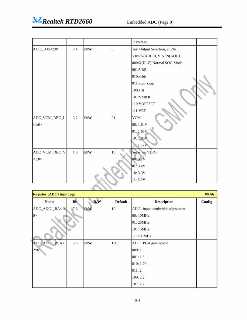
Realtek RTD2660 Embedded ADC (Page 0)
101
1: voltage
ADC_TOS<2:0> 6:4 R/W 0 Test Output Selection, at PIN
VIN2N(ADC0), VIN3N(ADC1)
000:X(Hi-Z) Normal SOG Mode
001:VRB
010:vrbb
011:vcm_cmp
100:vrtt
101:VMIDI
110:VOFFSET
111:VRT
ADC_VCM_DEC_I
<1:0>
3:2 R/W 01 VCM
00: 1.64V
01: 1.65V
10: 1.66V
11: 1.67V
ADC_VCM_DEC_V
<1:0>
1:0 R/W 10 Set when VDD=
00: 3.2V
01: 3.4V
10: 3.3V
11: 3.0V
Register::ADC1 input pga 0XA6
Name Bit R/W Default Description Config
ADC_ADC1_BA<1:
0>
7:6 R/W 10 ADC1 input bandwidth adjustment
00: 10MHz
01: 25MHz
10: 75MHz
11: 200MHz
ADC_ADC1_PGA<
2:0>
5:3 R/W 100 ADC1 PGA gain adjust
000: 1
001: 1.3
010: 1.76
011: 2
100: 2.3
101: 2.7

Realtek RTD2660 Embedded ADC (Page 0)
102
110: 3.27
111: 4.16
ADC_ADC1_CV<2:
0>
2:0 R/W 100 ADC1 channel clamp voltage
000: 0mV to 111: 700mV
Step: 100mV
Register::ADC0 input PGA 0XA7
Name Bit R/W Default Description Config
ADC_ADC0_BA<1:
0>
7:6 R/W 10 ADC0 input bandwidth adjustment
00: 10MHz
01: 25MHz
10: 75MHz
11: 200MHz
ADC_ADC0_PGA<
2:0>
5:3 R/W 100 ADC0 PGA gain adjust
000: 1
001: 1.3
010: 1.76
011: 2
100: 2.3
101: 2.7
110: 3.27
111: 4.16
ADC_ADC0_CV<2:
0>
2:0 R/W 100 ADC0 channel clamp voltage
000: 0mV to 111: 700mV
Step: 100mV
Register::VADC CLAMP 0XA8
Name Bit R/W Default Description Config
Rev 7:5 --- --- Reserved
ADC_OFFLINE_SR
C
4 R/W 1 OFFLINE clamp source(SOY1)
0: 100mV
1: 400mV
ADC_ADC1_CMS<
1:0>
3:2 R/W 0 ADC1 channel clamp mode selection
00: clamp to black- Low clamp
01: clamp to black-Middle clamp
10: clamp to sync

Realtek RTD2660 Embedded ADC (Page 0)
103
11: clamp to top
ADC_ADC0_CMS<
1:0>
1:0 R/W 0 ADC0 channel clamp mode selection
00: clamp to black- Low clamp
01: clamp to black-Middle clamp
10: clamp to sync
11: clamp to top
Register::ADC inrange CTRL 0XA9
Name Bit R/W Default Description Config
ADC_INRANGE<1:
0>
7:6 R/W 11 ADC1,0 Vmid, Voffset Voltage Adjust
0: Vmid=0V/0.75V/1.5V, Voffset=0.75V
1: Vmid=0V/0.5V/1.0V, Voffset=0.5V
Rev --- --- --- Reserved
ADC_VDC_CLAMP
_SP<4:0>
4:0 R/W 1 VDC clamping current control
I=20uA*sp<3:0>+10uA, shunt ohm if
sp<4> is 1
Address 0xAA are reserved
Register::ADC1 SOY BIAS CURRENT 0XAB
Name Bit R/W Default Description Config
Rev 7:6 --- --- Reserved
ADC_SOYBIAS1<1
:0>
5:4 R/W 1 Bias Current of SOY_6bitADC1 S/H
00:15u
01:20u
10:25u
11:30u
ADC_SRCBIAS<3:0
>
3:0 R/W 0X08 ADC<1:0> Mbias (MDAC+Buffer)
source current select
0000=20u, 0001=22.5u,
0010=25u, 0011=27.5u
0100=30u, 0101=32.5u,
0110=35u, 0111=37.5u
1000=40u, 1001=42.5u,
1010=45u, 1011=47.5u
1100=50u, 1101=52.5u,
1110=55u, 1111=57.5u

Realtek RTD2660 Embedded ADC (Page 0)
104
Register::ADC INPUT CHANNEL BIAS CURRENT 0XAC
Name Bit R/W Default Description Config
ADC_CHBIAS<3:0> 7:4 R/W 0X08 VIN<3:0><P,N> Input Channel bias
current select
0000=20u, 0001=22.5u,
0010=25u, 0011=27.5u
0100=30u, 0101=32.5u,
0110=35u, 0111=37.5u
1000=40u, 1001=42.5u,
1010=45u, 1011=47.5u
1100=50u, 1101=52.5u,
1110=55u, 1111=57.5u
ADC_BIAS<3:0> 3:0 R/W 0X08 AFE_MBIAS/SOY bias current select
0000=20u, 0001=22.5u, 0010=25u, 0011=27.5u 0100=30u, 0101=32.5u, 0110=35u, 0111=37.5u 1000=40u, 1001=42.5u, 1010=45u, 1011=47.5u 1100=50u, 1101=52.5u, 1110=55u, 1111=57.5u
Register::Posive Input SOY Restore Resistor 0XAD
Name Bit R/W Default Description Config
ADC_SOYDCR_EN
<3:0>
7:4 R/W 0 Vin3(bit3) to Vin0(bit0)SOY DC restore
enable
ADC_SOYR<3:0> 3:0 R/W 0 VIN<3:0>P Positive Input SOY DC
Restore Resistor
0: Poly R=500K,external C=10n
1: MOS R=1M,external C=4.7n
Register:: ADC POW 0XAE
Name Bit R/W Default Description Config
ADC_YPP_POW<3: 7:4 R/W 0 YPbPr clamp 3..0 power on

Realtek RTD2660 Embedded ADC (Page 0)
105
0> 0: power down 1: power on
ADC_VDC_POW<3
:0>
3:0 R/W 0 VDC clamp 3..0 power on
0: power down 1: power on
Register::VADC/Video-8 switch 0XAF
Name Bit R/W Default Description Config
REV 7 --- --- Reserved
ADC_PADEN 6 R/W 0 REG_ADC_PADEN
VADC/Video8 Switch (0: VADC
1:Video8)
ADC_BUFOPOW 5 R/W 0 Buffer out power on(AV out enable)
0: power down 1: power on
ADC_SOYCLPOW<
1:0>
4:3 R/W 0 SOY Compare<1:0> power on
0: power down 1: power on
ADC_ADCPOW<1:
0>
2:1 R/W 0 ADC power on (ADC_ADCPOW[0]
must be always high while video decoder
is enabled, otherwise, the clock for video
decoder will not be output)
0: power down 1: power on
ADC_GLPOW 0 R/W 1 GLOBAL power on
0: power down 1: power on
Address 0xB0~0xBF are reserved
Embedded YPP ADC
Register::red gain 0XC0
Name Bit R/W Default Description Config
ADC_GAI_RED[7:0
]
7:0 R/W 0x80 Red Channel Gain Adjust
Register::green gain 0XC1
Name Bit R/W Default Description Config
ADC_GAI_GRN[7:0
]
7:0 R/W 0x80 Green Channel Gain Adjust
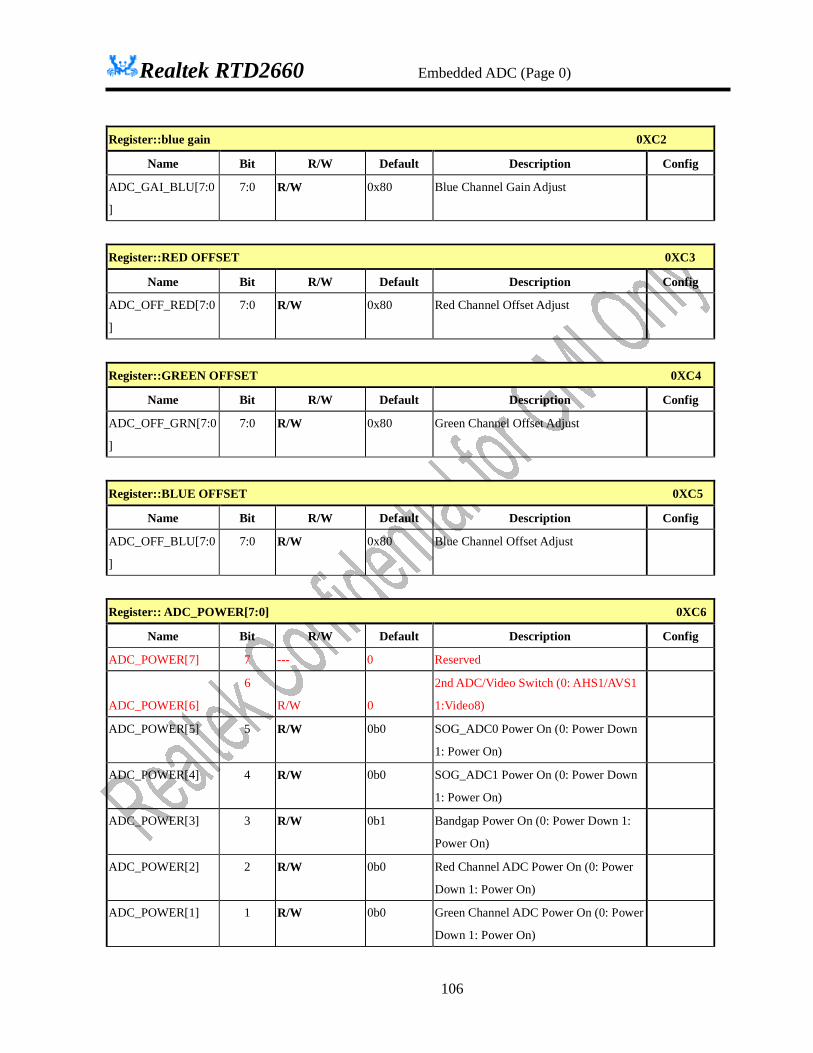
Realtek RTD2660 Embedded ADC (Page 0)
106
Register::blue gain 0XC2
Name Bit R/W Default Description Config
ADC_GAI_BLU[7:0
]
7:0 R/W 0x80 Blue Channel Gain Adjust
Register::RED OFFSET 0XC3
Name Bit R/W Default Description Config
ADC_OFF_RED[7:0
]
7:0 R/W 0x80 Red Channel Offset Adjust
Register::GREEN OFFSET 0XC4
Name Bit R/W Default Description Config
ADC_OFF_GRN[7:0
]
7:0 R/W 0x80 Green Channel Offset Adjust
Register::BLUE OFFSET 0XC5
Name Bit R/W Default Description Config
ADC_OFF_BLU[7:0
]
7:0 R/W 0x80 Blue Channel Offset Adjust
Register:: ADC_POWER[7:0] 0XC6
Name Bit R/W Default Description Config
ADC_POWER[7] 7 --- 0 Reserved
ADC_POWER[6]
6
R/W 0
2nd ADC/Video Switch (0: AHS1/AVS1
1:Video8)
ADC_POWER[5] 5 R/W 0b0 SOG_ADC0 Power On (0: Power Down
1: Power On)
ADC_POWER[4] 4 R/W 0b0 SOG_ADC1 Power On (0: Power Down
1: Power On)
ADC_POWER[3] 3 R/W 0b1 Bandgap Power On (0: Power Down 1:
Power On)
ADC_POWER[2] 2 R/W 0b0 Red Channel ADC Power On (0: Power
Down 1: Power On)
ADC_POWER[1] 1 R/W 0b0 Green Channel ADC Power On (0: Power
Down 1: Power On)

Realtek RTD2660 Embedded ADC (Page 0)
107
ADC_POWER[0] 0 R/W 0b0 Blue Channel ADC Power On (0: Power
Down 1: Power On)
Register:: ADC_IBIAS0[7:0] 0XC7
Name Bit R/W Default Description Config
ADC_IBIAS0[7:6] 7:6 R/W 0b01 Bias Current of M2PLL_IB20U (00:16u
01:20u 10:24u 11:28u)
Bias Current of DPLL_IB20U (00:16u
01:20u 10:24u 11:28u)
Bias Current of AUDIOPLL_IB20U
(00:16u 01:20u 10:24u 11:28u)
ADC_IBIAS0[5:4] 5:4 R/W 0b01 Bias Current of HSYNC_IB60U (00:48u
01:60u 10:72u 11:84u)
Adjust Hsync level
ADC_IBIAS0[3:2] 3:2 R/W 0b01 Bias Current of LVDS_IB20U (00:16u
01:20u 10:24u 11:28u)
ADC_IBIAS0[1] 1 R/W 0b0 Reserved
ADC_IBIAS0[0] 0 R/W 0b1 SOG0 input MUX select, high bit
Register:: ADC_IBIAS1[7:0] 0XC8
Name Bit R/W Default Description Config
ADC_IBIAS1[7:6] 7:6 R/W 0b00 SOG0 input MUX select, low 2 bits
(000: SOG1 001:B1 010:G1 011:R1
100: SOG0 101:B0 110:G0 111:R0
ADC_IBIAS1[5:4] 5:4 R/W 0b01 Bias Current of SOG_ADC_IB20U
(00:15u 01:20u 10:25u 11:30u)
ADC_IBIAS1[3:2] 3:2 R/W 0b01 Bias Current of CEC_IB10U (00:8u
01:10u 10:12u 11:14u)
ADC_IBIAS1[1:0] 1:0 R/W 0b01 Bias Current of SARADC_IB20U
(00:16u 01:20u 10:24u 11:28u)
Register:: ADC_IBIAS2[7:0] 0XC9
Name Bit R/W Default Description Config
ADC_IBIAS2[7:6] 7:6 R/W 0b01 Bias Current of APLL_IB60U (00:48u
01:60u 10:72u 11:84u)

Realtek RTD2660 Embedded ADC (Page 0)
108
ADC_IBIAS2[5:4] 5:4 R/W 0b01 Bias Current of ADC_SF (00:15u 01:20u
10:25u 11:30u)
ADC_IBIAS2[3] 3 R/W 0b0 Bias Current of ADC_REF (0:60u 1:80u)
ADC_IBIAS2[2:0] 2:0 R/W 0b011 Bias Current of ADC_OP
(000:10u 001:15u 010:17.5u 011:20u
100:22.5u 101:25u 110:27.5u 111:30u)
Register:: ADC_VBIAS0[7:0] 0XCA
Name Bit R/W Default Description Config
ADC_VBIAS0[7] 7 R/W 0b0 Resistor Reference (0:Ref. To Internal R
1:Ref. To External R=2K, for FIB)
ADC_VBIAS0[6:4] 6:4 R/W 0b010 Bandgap Voltage
(000:0.890 001:0.841 010:0.792
011:0.742 100:0.693 101:0.644 110:0.594
111:545)
ADC_VBIAS0[3:2] 3:2 R --- Thermal Sensor (00:<30 01:30-60
10:60-90 11>90)
ADC_VBIAS0[1:0] 1:0 R/W 0b01 Bandgap Voltage (00:0.775 01:0.792
10:0.810 11:0.829)
Register:: ADC_VBIAS1[7:0] 0XCB
Name Bit R/W Default Description Config
ADC_VBIAS1[7] 7 R/W 0b0 ADC Gain Calibration (0: Normal 1:
Calibration)
ADC_VBIAS1[6] 6 R/W 0b0 ADC 2X OverSample (0:1x 1:2x)
ADC_VBIAS1[5] 5 R/W 0b0 Output 1X Clock Polarity (0:Normal
1:Inverted)
ADC_VBIAS1[4] 4 R/W 0b0 Output 2X Clock Polarity (0:Normal
1:Inverted)
ADC_VBIAS1[3] 3 R/W 0b1 RGB Input Range Adjust
0: 0.3V-1.2V, 1: 0.5V-1.0V
ADC_VBIAS1[2] 2 R/W 0b1 Vcmo from VBG or from VDD (0:from
VBG 1:from VDD)
ADC_VBIAS1[1:0] 1:0 R/W 0b01 Vcmo Voltage (00:0.90 01:1.00 1:1.05
11:1.10)

Realtek RTD2660 Embedded ADC (Page 0)
109
Register:: ADC_CLOCK[7:0] 0XCC
Name Bit R/W Default Description Config
ADC_CLOCK[7] 7 R/W 0b0 Input Clock Polarity (0:Negative
1:Positive)
ADC_CLOCK[6] 6 R/W 0b0 Output Divider Clock Polarity (0:Normal
1:Inverted)
ADC_CLOCK[5:4] 5:4 R/W 0b0 ADC_OUT_PIXEL Delay (00:1.05n
01:1.39n 10:1.69n 11:1.97n)
ADC_CLOCK[3] 3 R/W 0b0 1X or 2X from APLL (0:1X 1:2X)
ADC_CLOCK[2] 2 R/W 0b0 Single Ended or Diff. Clock from APLL
(0:Diff. 1:Single Ended)
ADC_CLOCK[1:0] 1:0 R/W 0b1 Duty Stablizer
Register:: ADC_TEST[7:0] 0XCD
Name Bit R/W Default Description Config
ADC_TEST[7] 7 R/W
0b0 Clock Input (0: from APLL/3.3V 1: from
TTL/1.8V)
ADC_TEST[6:4]
6:4 R/W
0b000
Test Ouput Selection (PAD: SOGIN0,
SOGIN1)
SOGIN0 (000:X 001:gnd 010:vrbir
011:vcmi 100:vrtir 101:vmid 110:voffset
111:vdd)
SOGIN1 (000:X 001:gnd 010:vrefn
011:vcmo 100:vrefp 101:gnd 110:gnd
111:vdd)
ADC_TEST[3] 3 R/W
0b0 SOG1 ADC&DAC Calibration (0:
Normal 1: Calibration)
ADC_TEST[2] 2 R/W
0b0 SOG1 ADC output data pos/neg (0: pos
1:neg)
ADC_TEST[1:0] 1:0 R/W
0b00 Clock Output Divider (00: 1/1 01: 1/2 10:
1/3 11: 1/4)
Register:: ADC_CTL_RGB[7:0] 0XCE
Name Bit R/W Default Description Config
ADC_CTL_RGB 7:6 R/W 0b01 PGA (00: Ash=0.9 01: Ash=1.0 10:

Realtek RTD2660 Embedded ADC (Page 0)
110
[7:6] Ash=1.1 11: Ash=1.2)
ADC_CTL_RGB[5:4]
5:4: R/W
0b01 PGA (00: Aref=0.9 01: Aref=1.0 10:
Aref=1.1 11: Aref=1.2)
ADC_CTL_RGB[3]
3 R/W
0b0
Dual (0: Input0 1: Input1)
( Need to Select the Corresponding
ADC_OUT_SOG0/1)
ADC_CTL_RGB[2]
2 R/W
0b1 Single Ended or Diff. Input (0: Single
Ended 1: Diff)
ADC_CTL_RGB[1:0]
1:0 R/W
0b10 Bandwidth (00: 75M 01: 150M 10:
300M 11: 500M)
Register:: ADC_CTL_RED[7:0] 0XCF
Name Bit R/W Default Description Config
ADC_CTL_RED[7] 7
R/W
0b0
Clamp Voltage Source Select (0: Input0: VONLINE, Input1: VOFFLINE 1: Input0: VOFFLINE, Input1: VONELINE)
ADC_CTL_RED[6:4] 6:4
R/W
0b101 Clamp Voltage, VONLINE (0V~700mV, Step=100mV)
ADC_CTL_RED[3] 3
R/W
0b0
Offset Depends on Gain (0: RGB Yes, YPrPb No 1:RGB No, YPrPb No)
ADC_CTL_RED[2:0
]
2:0 R/W 0b0 Red Channel ADC Fine Tune Delay,
Step=90ps
Register:: ADC_CTL_GRN[7:0] 0XD0
Name Bit R/W Default Description Config
ADC_CTL_GRN[7] 7
R/W
0b0
Clamp Voltage Source Select (0: Input0: VONLINE, Input1: VOFFLINE 1: Input0: VOFFLINE, Input1: VONELINE)
ADC_CTL_GRN[6:4] 6:4
R/W
0b101 Clamp Voltage, VONLINE (0V~700mV, Step=100mV)
ADC_CTL_GRN 3 R/W 0b0 Offset Depends on Gain
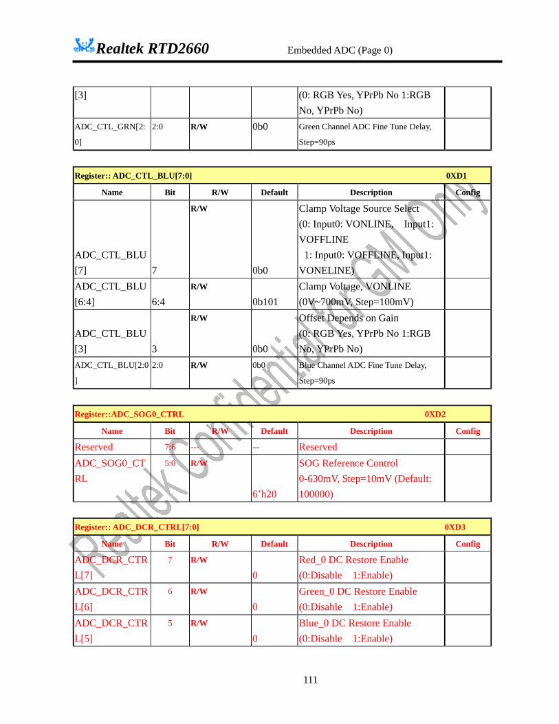
Realtek RTD2660 Embedded ADC (Page 0)
111
[3] (0: RGB Yes, YPrPb No 1:RGB No, YPrPb No)
ADC_CTL_GRN[2:
0]
2:0 R/W 0b0 Green Channel ADC Fine Tune Delay,
Step=90ps
Register:: ADC_CTL_BLU[7:0] 0XD1
Name Bit R/W Default Description Config
ADC_CTL_BLU[7] 7
R/W
0b0
Clamp Voltage Source Select (0: Input0: VONLINE, Input1: VOFFLINE 1: Input0: VOFFLINE, Input1: VONELINE)
ADC_CTL_BLU[6:4] 6:4
R/W
0b101 Clamp Voltage, VONLINE (0V~700mV, Step=100mV)
ADC_CTL_BLU[3] 3
R/W
0b0
Offset Depends on Gain (0: RGB Yes, YPrPb No 1:RGB No, YPrPb No)
ADC_CTL_BLU[2:0
]
2:0 R/W 0b0 Blue Channel ADC Fine Tune Delay,
Step=90ps
Register::ADC_SOG0_CTRL 0XD2
Name Bit R/W Default Description Config
Reserved 7:6 --- -- Reserved
ADC_SOG0_CTRL
5:0 R/W
6’h20
SOG Reference Control 0-630mV, Step=10mV (Default: 100000)
Register:: ADC_DCR_CTRL[7:0] 0XD3
Name Bit R/W Default Description Config
ADC_DCR_CTRL[7]
7 R/W
0 Red_0 DC Restore Enable (0:Disable 1:Enable)
ADC_DCR_CTRL[6]
6 R/W
0 Green_0 DC Restore Enable (0:Disable 1:Enable)
ADC_DCR_CTRL[5]
5 R/W
0 Blue_0 DC Restore Enable (0:Disable 1:Enable)
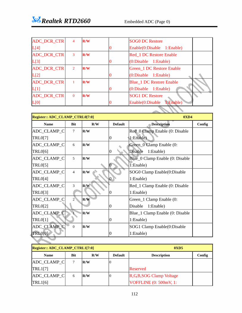
Realtek RTD2660 Embedded ADC (Page 0)
112
ADC_DCR_CTRL[4]
4 R/W
0 SOG0 DC Restore Enable(0:Disable 1:Enable)
ADC_DCR_CTRL[3]
3 R/W
0 Red_1 DC Restore Enable (0:Disable 1:Enable)
ADC_DCR_CTRL[2]
2 R/W
0 Green_1 DC Restore Enable (0:Disable 1:Enable)
ADC_DCR_CTRL[1]
1 R/W
0 Blue_1 DC Restore Enable (0:Disable 1:Enable)
ADC_DCR_CTRL[0]
0 R/W
0 SOG1 DC Restore Enable(0:Disable 1:Enable)
Register:: ADC_CLAMP_CTRL0[7:0] 0XD4
Name Bit R/W Default Description Config
ADC_CLAMP_CTRL0[7]
7 R/W
0 Red_0 Clamp Enable (0: Disable 1:Enable)
ADC_CLAMP_CTRL0[6]
6 R/W
0 Green_0 Clamp Enable (0: Disable 1:Enable)
ADC_CLAMP_CTRL0[5]
5 R/W
0 Blue_0 Clamp Enable (0: Disable 1:Enable)
ADC_CLAMP_CTRL0[4]
4 R/W
0 SOG0 Clamp Enable(0:Disable 1:Enable)
ADC_CLAMP_CTRL0[3]
3 R/W
0 Red_1 Clamp Enable (0: Disable 1:Enable)
ADC_CLAMP_CTRL0[2]
2 R/W
0 Green_1 Clamp Enable (0: Disable 1:Enable)
ADC_CLAMP_CTRL0[1]
1 R/W
0 Blue_1 Clamp Enable (0: Disable 1:Enable)
ADC_CLAMP_CTRL0[0]
0 R/W
0 SOG1 Clamp Enable(0:Disable 1:Enable)
Register:: ADC_CLAMP_CTRL1[7:0] 0XD5
Name Bit R/W Default Description Config
ADC_CLAMP_CTRL1[7]
7 R/W 0
Reserved
ADC_CLAMP_CTRL1[6]
6 R/W 0 R,G,B,SOG Clamp Voltage VOFFLINE (0: 500mV, 1:
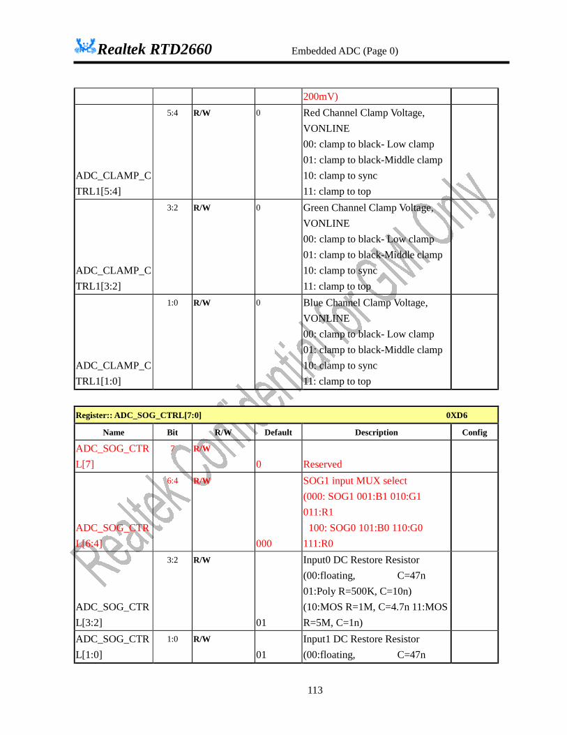
Realtek RTD2660 Embedded ADC (Page 0)
113
200mV)
ADC_CLAMP_CTRL1[5:4]
5:4 R/W 0 Red Channel Clamp Voltage, VONLINE 00: clamp to black- Low clamp 01: clamp to black-Middle clamp 10: clamp to sync 11: clamp to top
ADC_CLAMP_CTRL1[3:2]
3:2 R/W 0 Green Channel Clamp Voltage, VONLINE 00: clamp to black- Low clamp 01: clamp to black-Middle clamp 10: clamp to sync 11: clamp to top
ADC_CLAMP_CTRL1[1:0]
1:0 R/W 0 Blue Channel Clamp Voltage, VONLINE 00: clamp to black- Low clamp 01: clamp to black-Middle clamp 10: clamp to sync 11: clamp to top
Register:: ADC_SOG_CTRL[7:0] 0XD6
Name Bit R/W Default Description Config
ADC_SOG_CTRL[7]
7 R/W
0 Reserved
ADC_SOG_CTRL[6:4]
6:4 R/W
000
SOG1 input MUX select (000: SOG1 001:B1 010:G1 011:R1 100: SOG0 101:B0 110:G0 111:R0
ADC_SOG_CTRL[3:2]
3:2 R/W
01
Input0 DC Restore Resistor (00:floating, C=47n 01:Poly R=500K, C=10n) (10:MOS R=1M, C=4.7n 11:MOS R=5M, C=1n)
ADC_SOG_CTRL[1:0]
1:0 R/W
01 Input1 DC Restore Resistor (00:floating, C=47n
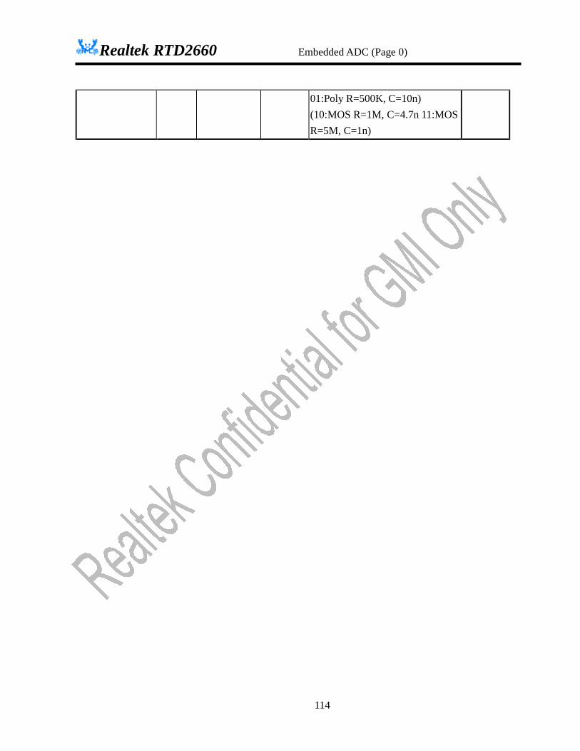
Realtek RTD2660 Embedded ADC (Page 0)
114
01:Poly R=500K, C=10n) (10:MOS R=1M, C=4.7n 11:MOS R=5M, C=1n)
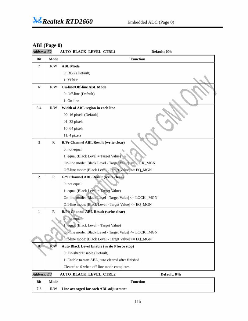
Realtek RTD2660 Embedded ADC (Page 0)
115
ABL(Page 0) Address: E2 AUTO_BLACK_LEVEL_CTRL1 Default: 00h
Bit Mode Function
7 R/W ABL Mode
0: RBG (Default)
1: YPbPr
6 R/W On-line/Off-line ABL Mode
0: Off-line (Default)
1: On-line
5:4 R/W Width of ABL region in each line
00: 16 pixels (Default)
01: 32 pixels
10: 64 pixels
11: 4 pixels
3 R R/Pr Channel ABL Result (write clear)
0: not equal
1: equal (Black Level = Target Value)
On-line mode: |Black Level - Target Value| <=LOCK_MGN
Off-line mode: |Black Level - Target Value| <= EQ_MGN 2 R G/Y Channel ABL Result (write clear)
0: not equal
1: equal (Black Level = Target Value)
On-line mode: |Black Level - Target Value| <= LOCK _MGN
Off-line mode: |Black Level - Target Value| <= EQ_MGN
1 R B/Pb Channel ABL Result (write clear)
0: not equal
1: equal (Black Level = Target Value)
On-line mode: |Black Level - Target Value| <= LOCK _MGN
Off-line mode: |Black Level - Target Value| <= EQ_MGN
0 R/W Auto Black Level Enable (write 0 force stop)
0: Finished/Disable (Default)
1: Enable to start ABL, auto cleared after finished
Cleared to 0 when off-line mode completes.
Address: E3 AUTO_BLACK_LEVEL_CTRL2 Default: 84h
Bit Mode Function
7:6 R/W Line averaged for each ABL adjustment

Realtek RTD2660 Embedded ADC (Page 0)
116
00: 8
01: 16
10: 32 (Default)
11: 64
5 -- Reserved
4:0 R/W Start Vertical Position of ABL in each line
Determine the start line of auto-black-level after the leading edge of Vsync
Address: E4 AUTO_BLACK_LEVEL_CTRL3 Default: 10h
Bit Mode Function
7:4 R/W Y/R/G/B Target value
0000: 1
0001: 2 (Default)
0010: 3
0011: 4
….
1111:16
(Pb/Pr Target level is fixed 128)
3:2 R/W Lock Margin
00: 1 (Default)
01: 2
10: 4
11: 6
1:0 R/W End Vertical Position of ABL measurement region [9:8]
Determine the last line of auto-black-level measurement for every frame/field countd by double
line
Address: E5 AUTO_BLACK_LEVEL_CTRL4 Default: 82h
Bit Mode Function
7:0 R/W End Vertical Position of ABL measurement region [7:0]
Determine the last line of auto-black-level measurement for every frame/field counted by double
line.
Address: E6 AUTO_BLACK_LEVEL_CTRL5 Default: 04h
Bit Mode Function
7:0 R/W Start Position of ABL in Each Line
Determine the start position of auto-black-level after the trailing edge of reference signal.
(When ABL mode in YPbPr, the reference signal is input Hsync. In RGB mode, the reference
signal is clamp signal.)
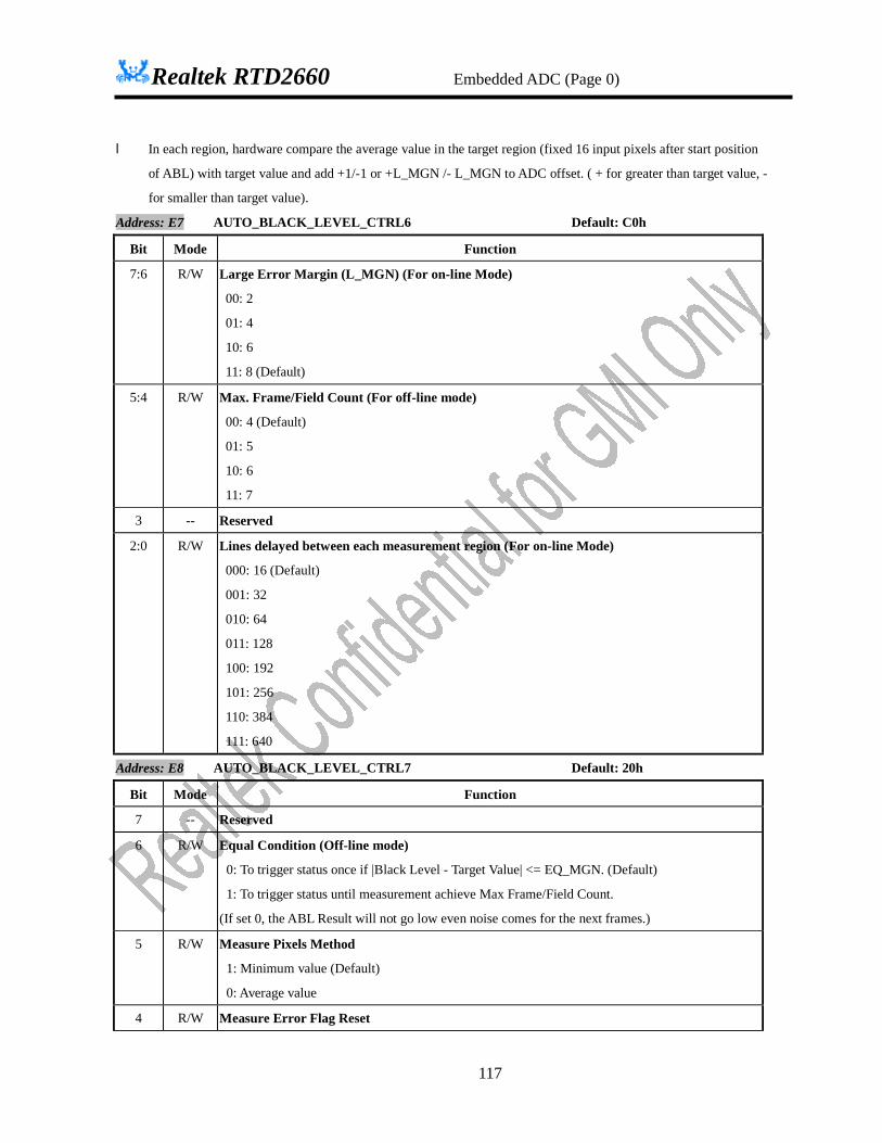
Realtek RTD2660 Embedded ADC (Page 0)
117
l In each region, hardware compare the average value in the target region (fixed 16 input pixels after start position
of ABL) with target value and add +1/-1 or +L_MGN /- L_MGN to ADC offset. ( + for greater than target value, -
for smaller than target value).
Address: E7 AUTO_BLACK_LEVEL_CTRL6 Default: C0h
Bit Mode Function
7:6 R/W Large Error Margin (L_MGN) (For on-line Mode)
00: 2
01: 4
10: 6
11: 8 (Default)
5:4 R/W Max. Frame/Field Count (For off-line mode)
00: 4 (Default)
01: 5
10: 6
11: 7
3 -- Reserved
2:0 R/W Lines delayed between each measurement region (For on-line Mode)
000: 16 (Default)
001: 32
010: 64
011: 128
100: 192
101: 256
110: 384
111: 640
Address: E8 AUTO_BLACK_LEVEL_CTRL7 Default: 20h
Bit Mode Function
7 -- Reserved
6 R/W Equal Condition (Off-line mode)
0: To trigger status once if |Black Level - Target Value| <= EQ_MGN. (Default)
1: To trigger status until measurement achieve Max Frame/Field Count.
(If set 0, the ABL Result will not go low even noise comes for the next frames.)
5 R/W Measure Pixels Method
1: Minimum value (Default)
0: Average value
4 R/W Measure Error Flag Reset
Realtek RTD2660 Embedded ADC (Page 0)
118
0: Normal
1: Reset
3 R Measure Error Flag
0: Normal
1: Error
(This flag is occurred when Hsync trailing edge is met during measurement.)
2 R/W Hsync Start Reference Select
0: HS leading edge (Default)
1: HS trailing edge
1:0 R/W Equal margin (EQ_MGN)
00: 0 (Default)
01: 1
10: 2
11: 3
Address: E9 AUTO_BLACK_LEVEL_RED_VALUE
Bit Mode Function
7:0 R Minimum/Average Value of Red Channel in Test Mode
Address: EA AUTO_BLACK_LEVEL_GREEN_VALUE
Bit Mode Function
7:0 R Minimum/Average Value of Green Channel in Test Mode
Address: EB AUTO_BLACK_LEVEL_BLUE_VALUE
Bit Mode Function
7:0 R Minimum/Average Value of Blue Channel in Test Mode
Address: EC AUTO_BLACK_LEVEL_NOISE_VALUE_OF_RED_CHANNEL
Bit Mode Function
7:0 R Noise Value of Red Channel in Test Mode after Equal status is triggered.
Address: ED AUTO_BLACK_LEVEL_NOISE_VALUE_OF_GREEN_CHANNEL
Bit Mode Function
7:0 R Noise Value of Green Channel in Test Mode after Equal status is triggered.
Address: EE AUTO_BLACK_LEVEL_NOISE_VALUE_OF_BLUE_CHANNEL
Bit Mode Function
7:0 R Noise Value of Blue Channel in Test Mode after Equal status is triggered.
Address 0xEF~0xF2 are reserved
Realtek RTD2660 Embedded ADC (Page 0)
119
LVR(Page 0) Address: F3 POWER_ON_RESET Default:94h
Bit Mode Function
7:6 R/W Negative Threshold Value For Power on Reset
00:1.8V
01:2.0V
10:2.2V(Default)
11:2.4V
5:0 R/W Reserved to 0
Schmitt trigger Address:F4 HS_SCHMITT_TRIGGE_CTRL Default:E1h
Bit Mode Function
7 R/W HSYNC Schmitt Power Down (Only for Schmitt trigger new mode)
0: Power down
1: Normal (Default)
6 R/W Polarity Select
0: Negative HSYNC (high level)
1: Positive HSYNC (low level) (Default)
5 R/W Schmitt Trigger Mode
0: Reserved
1: New mode
4 R/W Threshold Voltage Fine Tune (only for Schmitt trigger new mode)
0: 0V (Default)
1: -0.1V
3:2 R/W Positive Threshold Voltage
1:0 R/W Negative Threshold Voltage l There is a mode of the HSYNC Schmitt trigger.
1. New mode: Fully programmable Schmitt trigger. The following table will determine the Schmitt Trigger positive and negative voltage: bit[6]=1 (Positive HSYNC) bit[6] = 0 (Negative HSYNC) bit[3:2] Vt
+ bit[1:0] Vt- bit[3:2] Vt
+ bit[1:0] Vt-
00 1.4V 00 Vt+ - 1.2V 00 1.8V 00 Vt
+ - 1.2V 01 1.6V 01 Vt
+ - 1.0V 01 2.0V 01 Vt+ - 1.0V
10 1.8V 10 Vt+ - 0.8V 10 2.2V 10 Vt
+ - 0.8V 11 2.0V 11 Vt
+ - 0.6V 11 2.4V 11 Vt+ - 0.6V
l After we get the threshold voltage by the table, we still can fine tune it: Final Positive Threshold Voltage = Vt
+ - 0.1* bit[4] Final Negative Threshold Voltage = Vt
-- 0.1* bit[4]

Realtek RTD2660 ADC PLL (Page 1)
120
ADC PLL (Page 1) Address: A0 PLL_DIV_CTRL Default: 08h
Bit Mode Function 7 R/W DDS Tracking Edge
0: HS positive edge (Default) 1: HS negative edge
6 R/W Tracking direction inversion 0: if HS leads HSFB => phase lead => m, k↑(Default) 1: if HS lags HSFB => phase lag => m, k ↓
5:4 R/W Waiting HS lines to start counting divider for Fast Lock function 00: 4 (default) 01: 3 10: 2 11: 1
3:2 R/W Delay Compensation Mode 00: Mode 0 No delay from PLL phase0 to DDS pfd input 01: Mode 1
Delay the path from PLL phase0 to DDS pfd input to be around 4.2 ns 10: Mode 2 (default) Delay the path from PLL phase0 to DDS pfd input to be around 4.6 ns 11: Mode 3 Delay the path from PLL phase0 to DDS pfd input to be around 5 ns
1 R/W Reserved to 0 0 R/W Reserved to 0
Address: A1 I_CODE_M Default: 01h Bit Mode Function 7 R/W Reserved to 0
6:0 R/W I_CODE[14:8] Address: A2 I_CODE_L Default: 04h
Bit Mode Function 7:0 R/W I_CODE[7:0]
Address: A3 P_CODE Default: 20h Bit Mode Function 7:0 R/W P_CODE[7:0]
Address: A4 PFD_CALIBRATED_RESULTS_H Default: 8’b0xxxxxxx Bit Mode Function
7 R/W PFD Calibration Enable (auto clear when finished)
Overwrite 0 to 1 return a new PFD calibrated value. 6:4 R/W Reserved to 0 3:0 R PFD Calibrated Results [11:8]
Address: A5 PFD_CALIBRATED_RESULTS_L Default: 8’bxxxxxxxx Bit Mode Function
7:0 R PFD Calibrated Results [7:0]
Address: A6 PE_MEARSURE_H Default: 8’b0xxxxxxx

Realtek RTD2660 ADC PLL (Page 1)
121
Bit Mode Function 7 R/W PE Measure Enable (auto clear when finished)
0: Disable (Default)
1: Start PE Measurement, clear after finish. 6:4 R/W Reserved to 0 3:0 R PE Value Result [11:8]
Address: A7 PE_MEARSURE_L Default: 8’bxxxxxxxx Bit Mode Function 7:0 R PE Value Result [7:0]
Address: A8 PE_MAX_MEASURE_H Default: 8’b0xxxxxxx Bit Mode Function 7 R/W PE Max. Measure Enable
0: Disable (Default)
1: Start PE Max. Measurement 6:4 R/W Reserved to 0 3:0 R PE Max Value [11:8]
Address: A9 PE_MAX_MEASURE_L Default: 8’bxxxxxxxx Bit Mode Function 7:0 R PE Max Value [7:0]
Address: AA FAST_PLL_CTRL Default: 00h
Bit Mode Function 7 R/W PE Max. Measure Clear
0: clear (Default)
1: write ‘1’ to clear PE Max. Value
6 R/W Enable APLL Setting
0: Disable (Default)
1: Enable (Auto clear when finished)
When CR AA[5] enabled, enable this bit will write P_CODE, I_CODE, PLL M/N, PLL K,
PLLDIV and DDS SUM_I at the end of input vertical data enable
5 R/W Enable Fast PLL Mechanism
0: Disable (Default)
1: Enable (Auto clear when finished)
4 R/W Force APLL Setting Enable
Force to write PLL M/N, K, PLLDIV and SUM_I while got no V_ACTIVE signal 0: Disable (Default)
1: Enable (Auto clear when finished)
Realtek RTD2660 ADC PLL (Page 1)
122
3 R/W DDS SUM_I Setting Updated Enable
0: Disable (Default)
1: Enable (Auto clear when finished)
2 R/W Measure SUM_I
0: Disable
1: Enable (Auto clear after finish)
1 R/W Enable Port A3
0: Disable Port A3 Access
1: Enable Port A3 Access
When this bit is 0, port address will be reset to 00, and will auto increase when read or write
0 R/W Select SUM_I for Read
1: Select SUM_I_NOW [26:0] for read
0: Select SUM_I_PRE [26:0] for read
Address: AB FAST_PLL_SUM_I
Bit Mode Function
7:0 R/W SUM_I_PRE (Auto Increase)
1st [00000, SUM_I [26:24]]
2nd SUM_I [23:16]
3rd SUM_I [15:8]
4th SUM_I [7:0]
Address: AC PLL_M (M Parameter Register) Default: 09h Bit Mode Function
7:0 R/W PLLM 7:0] (PLL DPM value – 3)
Address: AD PLL_N (N Parameter Register) Default: 20h Bit Mode Function 7:4 R/W PLLSPHNEXT[3:0] (K) (default is 0000) 3 R/W PLLSNBP
0: N is followed by the value of REG A5 [3:1]
1: N is always 1 2:0 R/W PLLN[2:0] (PLL DPN value – 2) (default is 000)
It is supposed to be always bigger than 2 l PLL1_N modify to only 4-bit. l Assume PLL1_M=0x0B, P1M=0x0B+3=14; PLL1_N=0x03, P1N=0x03+2=5; K=7; F_IN = 24.576MHz. F_PLL
= F_IN x ( (P1M+7/16) / P1N ) = 24.576 x 14.4375 / 5 = 70.9632MHz l If the target frequency is F_ADC, the constraint of F_PLL is (M+-7/16)/N * XTCLK < F_PLL1 < (M+8/16)/N
*XTCLK l Although the new dds provides +15/-16 phase margin for tracking. However it is better not to set M, N and K to
be some freq. that PLL has to swallow +15/-16 phases. Because under that condition, SDM will get saturation problem.

Realtek RTD2660 ADC PLL (Page 1)
123
l For NO shrink IC => PLLN setting will have no limitation l For shrink IC and timing factor predicted as 0.8 => crystal clock 27 MHZ => PLLN can’t be 0 while APLL VCO
is lower than 167MHZ crystal clock 24.576 MHZ => PLLN can’t be 0 while APLL VCO is lower than 84 MHZ l For shrink IC and timing factor predicted as 0.9 => crystal clock 27 MHZ => PLLN can’t be 0 while APLL VCO
is lower than 74 MHZ crystal clock 24.576 MHZ => PLLN can’t be 0 while APLL VCO is lower than 52 MHZ Address: AE PLL_CRNT (PLL Current/Resistor Register) Default: 63h
Bit Mode Function 7:5 R/W PLLVR [2:0] (PLL Loop Filter Resister Control)
000: 20K
001: 21K
010: 22K
011: 23K (Default)
100: 24K
101: 25K
110: 26K
111: 27K 4:0 R/W PLLSI [4:0] (PLL Charger Pump Current IchDpll) (Default: 00011b)
Icp = 2.5uA+2.5uA*bit[0]+5uA*bit[1]+10uA*bit[2]+20uA*bit[3] l Keep Icp/DPM constant Address: AF PLL_WD (PLL Watch Dog Register) Default: 09h
Bit Mode Function 7 R PLLSTATUS (PLL WD Status)
0: Normal (Default)
1: Abnormal 6 R/W PLLWDRST (PLL WD Reset)
0: Normal (Default)
1: Reset 5 R/W PLLWDSET (PLL WD Set)
0: Normal (Default) 1: Set
4:3 R/W PLLWDVSET[1:0] (PLL WD Voltage Set)
00: 2.46V
01: 1.92V(Default)
10: 1.36V
11: 1.00V 2 R/W HS_dds2synp latch edge
0: falling edge (default)
Realtek RTD2660 ADC PLL (Page 1)
124
1: rising 1 R/W Reset DDS
0: normal (default) 1: reset whole DDS
0 R/W PLLPWDN (PLL Power Down) 0: Normal Run 1: Power Down (Default)
l HSFB_dds2synp & HS_dds2synp will be both sampled by AF [2] Address: B0 PLL_MIX Default: 8’b0000_000x
Bit Mode Function 7 R/W PLLSVR3 6 --- Reserved to 0 5 R/W PLLSVC3 4 --- Reserved to 0 3 --- Reserved to 0
2:1 R/W ADCKMODE [1:0] (ADC Input Clock Select Mode)
00: Single Clock Mode (Default)
01: Single Inverse-Clock Mode
10: External Clock Mode
11: Dual Clock Mode (1x and 2x Clock) 0 R Swallow phase enable (K mask disabled)
The pll can’t enable swallow phase function while pll just be power up. Waiting for 64 clock
cycles then start to enable phase swallow function.
While power down, the counter will be reset. While power up, the counter start to work Address: B1 PLLDIV_H Default: 45h
Bit Mode Function
7 --- Reserved to 0
6 R/W Phase_Select_Method
0: Manual
1: Look-Up-Table (default)
5 R/W PLLPH0PATH
0: Short Path (Default)
1: Long Path (Compensate PLL_ADC path delay)
4 R/W PLLD2
0:ADC CLK=1/2 VCO CLK (Default)
1:ADC CLK=1/4 VCO CLK
3:0 R/W PLL Divider Ratio Control. High-Byte [11:8]. (Default: 5h)
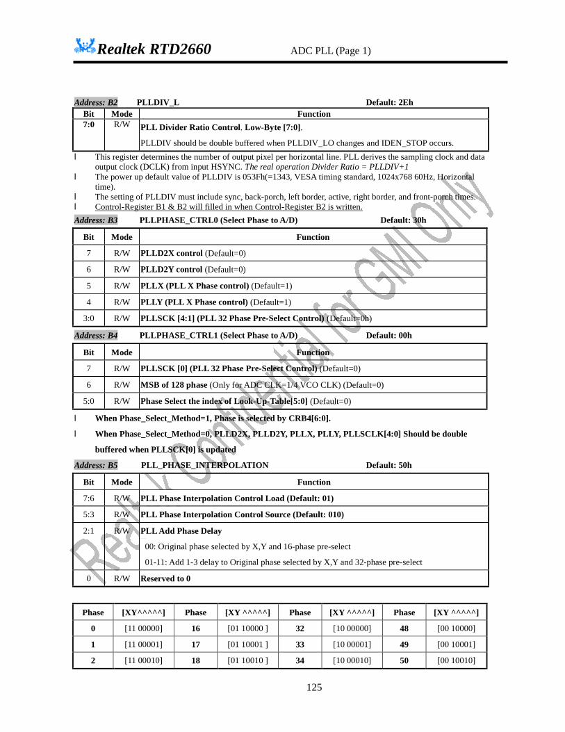
Realtek RTD2660 ADC PLL (Page 1)
125
Address: B2 PLLDIV_L Default: 2Eh
Bit Mode Function 7:0 R/W PLL Divider Ratio Control. Low-Byte [7:0].
PLLDIV should be double buffered when PLLDIV_LO changes and IDEN_STOP occurs. l This register determines the number of output pixel per horizontal line. PLL derives the sampling clock and data
output clock (DCLK) from input HSYNC. The real operation Divider Ratio = PLLDIV+1 l The power up default value of PLLDIV is 053Fh(=1343, VESA timing standard, 1024x768 60Hz, Horizontal
time). l The setting of PLLDIV must include sync, back-porch, left border, active, right border, and front-porch times. l Control-Register B1 & B2 will filled in when Control-Register B2 is written. Address: B3 PLLPHASE_CTRL0 (Select Phase to A/D) Default: 30h
Bit Mode Function
7 R/W PLLD2X control (Default=0)
6 R/W PLLD2Y control (Default=0)
5 R/W PLLX (PLL X Phase control) (Default=1)
4 R/W PLLY (PLL X Phase control) (Default=1)
3:0 R/W PLLSCK [4:1] (PLL 32 Phase Pre-Select Control) (Default=0h)
Address: B4 PLLPHASE_CTRL1 (Select Phase to A/D) Default: 00h
Bit Mode Function
7 R/W PLLSCK [0] (PLL 32 Phase Pre-Select Control) (Default=0)
6 R/W MSB of 128 phase (Only for ADC CLK=1/4 VCO CLK) (Default=0)
5:0 R/W Phase Select the index of Look-Up-Table[5:0] (Default=0)
l When Phase_Select_Method=1, Phase is selected by CRB4[6:0].
l When Phase_Select_Method=0, PLLD2X, PLLD2Y, PLLX, PLLY, PLLSCLK[4:0] Should be double
buffered when PLLSCK[0] is updated
Address: B5 PLL_PHASE_INTERPOLATION Default: 50h
Bit Mode Function
7:6 R/W PLL Phase Interpolation Control Load (Default: 01)
5:3 R/W PLL Phase Interpolation Control Source (Default: 010)
2:1 R/W PLL Add Phase Delay
00: Original phase selected by X,Y and 16-phase pre-select
01-11: Add 1-3 delay to Original phase selected by X,Y and 32-phase pre-select
0 R/W Reserved to 0
Phase [XY^^^^^] Phase [XY ^^^^^] Phase [XY ^^^^^] Phase [XY ^^^^^]
0 [11 00000] 16 [01 10000 ] 32 [10 00000] 48 [00 10000]
1 [11 00001] 17 [01 10001 ] 33 [10 00001] 49 [00 10001]
2 [11 00010] 18 [01 10010 ] 34 [10 00010] 50 [00 10010]
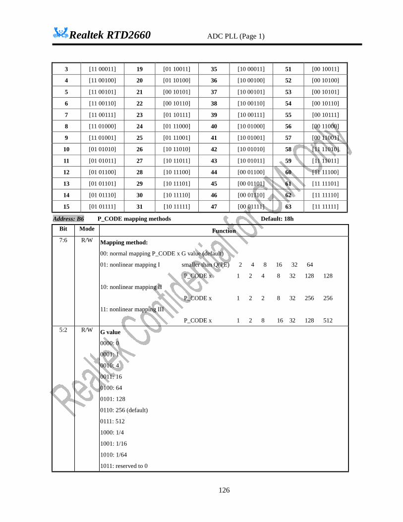
Realtek RTD2660 ADC PLL (Page 1)
126
3 [11 00011] 19 [01 10011] 35 [10 00011] 51 [00 10011]
4 [11 00100] 20 [01 10100] 36 [10 00100] 52 [00 10100]
5 [11 00101] 21 [00 10101] 37 [10 00101] 53 [00 10101]
6 [11 00110] 22 [00 10110] 38 [10 00110] 54 [00 10110]
7 [11 00111] 23 [01 10111] 39 [10 00111] 55 [00 10111]
8 [11 01000] 24 [01 11000] 40 [10 01000] 56 [00 11000]
9 [11 01001] 25 [01 11001] 41 [10 01001] 57 [00 11001]
10 [01 01010] 26 [10 11010] 42 [10 01010] 58 [11 11010]
11 [01 01011] 27 [10 11011] 43 [10 01011] 59 [11 11011]
12 [01 01100] 28 [10 11100] 44 [00 01100] 60 [11 11100]
13 [01 01101] 29 [10 11101] 45 [00 01101] 61 [11 11101]
14 [01 01110] 30 [10 11110] 46 [00 01110] 62 [11 11110]
15 [01 01111] 31 [10 11111] 47 [00 01111] 63 [11 11111]
Address: B6 P_CODE mapping methods Default: 18h Bit Mode Function 7:6 R/W Mapping method:
00: normal mapping P_CODE x G value (default)
01: nonlinear mapping I smaller than Q(PE) 2 4 8 16 32 64
P_CODE x 1 2 4 8 32 128 128
10: nonlinear mapping II
P_CODE x 1 2 2 8 32 256 256
11: nonlinear mapping III
P_CODE x 1 2 8 16 32 128 512 5:2 R/W G value
0000: 0
0001: 1
0010: 4
0011: 16
0100: 64
0101: 128
0110: 256 (default)
0111: 512
1000: 1/4
1001: 1/16
1010: 1/64
1011: reserved to 0
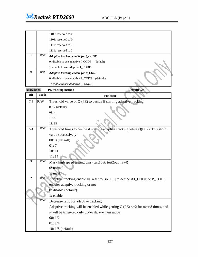
Realtek RTD2660 ADC PLL (Page 1)
127
1100: reserved to 0
1101: reserved to 0
1110: reserved to 0
1111: reserved to 0 1 R/W Adaptive tracking enable for I_CODE
0: disable to use adaptive I_CODE (default)
1: enable to use adaptive I_CODE 0 R/W Adaptive tracking enable for P_CODE
0: disable to use adaptive P_CODE (default)
1: enable to use adaptive P_CODE
Address: B7 PE tracking method Default: 02h Bit Mode Function
7:6 R/W Threshold value of Q (PE) to decide if starting adaptive tracking 00: 2 (default)
01: 4
10: 8
11: 15 5:4 R/W Threshold times to decide if starting adaptive tracking while Q(PE) < Threshold
value successively 00: 3 (default) 01: 7 10: 11 11: 15
3 R/W Mask high speed testing pins (test1out, test2out, fav4) 0: normal 1: mask
2 R/W Adaptive tracking enable => refer to B6 [1:0] to decide if I_CODE or P_CODE enables adaptive tracking or not 0: disable (default) 1: enable
1:0 R/W Decrease ratio for adaptive tracking Adaptive tracking will be enabled while getting Q (PE) <=2 for over 8 times, and it will be triggered only under delay-chain mode 00: 1/2 01: 1/4 10: 1/8 (default)
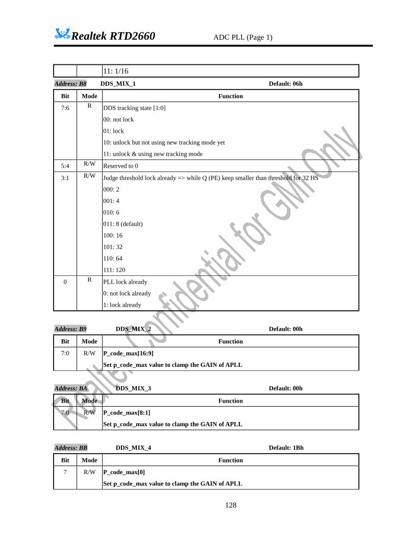
Realtek RTD2660 ADC PLL (Page 1)
128
11: 1/16 Address: B8 DDS_MIX_1 Default: 06h
Bit Mode Function
7:6 R DDS tracking state [1:0]
00: not lock
01: lock
10: unlock but not using new tracking mode yet
11: unlock & using new tracking mode
5:4 R/W Reserved to 0
3:1 R/W Judge threshold lock already => while Q (PE) keep smaller than threshold for 32 HS
000: 2
001: 4
010: 6
011: 8 (default)
100: 16
101: 32
110: 64
111: 120
0 R PLL lock already
0: not lock already
1: lock already
Address: B9 DDS_MIX_2 Default: 00h
Bit Mode Function
7:0 R/W P_code_max[16:9]
Set p_code_max value to clamp the GAIN of APLL
Address: BA DDS_MIX_3 Default: 00h
Bit Mode Function
7:0 R/W P_code_max[8:1]
Set p_code_max value to clamp the GAIN of APLL
Address: BB DDS_MIX_4 Default: 1Bh
Bit Mode Function
7 R/W P_code_max[0]
Set p_code_max value to clamp the GAIN of APLL
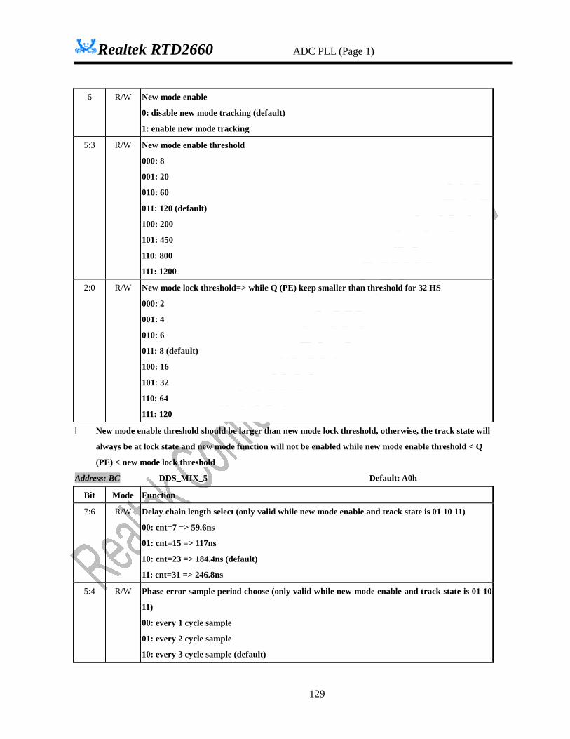
Realtek RTD2660 ADC PLL (Page 1)
129
6 R/W New mode enable
0: disable new mode tracking (default)
1: enable new mode tracking
5:3 R/W New mode enable threshold
000: 8
001: 20
010: 60
011: 120 (default)
100: 200
101: 450
110: 800
111: 1200
2:0 R/W New mode lock threshold=> while Q (PE) keep smaller than threshold for 32 HS
000: 2
001: 4
010: 6
011: 8 (default)
100: 16
101: 32
110: 64
111: 120
l New mode enable threshold should be larger than new mode lock threshold, otherwise, the track state will
always be at lock state and new mode function will not be enabled while new mode enable threshold < Q
(PE) < new mode lock threshold
Address: BC DDS_MIX_5 Default: A0h
Bit Mode Function
7:6 R/W Delay chain length select (only valid while new mode enable and track state is 01 10 11)
00: cnt=7 => 59.6ns
01: cnt=15 => 117ns
10: cnt=23 => 184.4ns (default)
11: cnt=31 => 246.8ns
5:4 R/W Phase error sample period choose (only valid while new mode enable and track state is 01 10
11)
00: every 1 cycle sample
01: every 2 cycle sample
10: every 3 cycle sample (default)

Realtek RTD2660 ADC PLL (Page 1)
130
11: every 4 cycle sample
3 R/W Delay chain reset period select 0: short reset (2ns) (default)
1: long reset (1 fbck)
2 R/W Reset delay chain saturation flag
0: normal (default)
1: reset flag
1 R Delay chain saturation flag 0: not saturate
1: saturate => it need to enlarge the sample period or set bigger N code
0 R/W APLL_free_run enable
0: normal state (default)
1: force APLL to free run state
l While we got delay chain saturation flag 1’b1, that means that the big jitter is bigger than what we image and we
have to reset the delay chain length setting BC [7:6]. Also we have to enlarge the sampling period & delay chain
length
l The choice for sampling period will be set by the rule as following:
(Delay chain length * 78 +50) * each tap delay + 10(ns) must be < N * TXCLK * sample period
if delay chain saturation flag goes high, then we must enlarge the delay chain length & set bigger sampling period
l While we enable free run mode, DDS will keep reset status until disable free run Address: BD DDS_MIX_6
Bit Mode Function
7:0 R Final M code to APLL
l While we like to read final M code & K code, we have to enable measure PE 9E[7] first. Otherwise we will get
glitch value
Address: BE DDS_MIX_7 Default: 00h
Bit Mode Function
7:4 R Final K code to APLL
3:1 R/W Change mode threshold => triggered by any Q (PE) > threshold
000: 600 (default)
001: 850
010: 1100
011: 1350
100: 1600
101: 1850
110: 2100
111: 2350

Realtek RTD2660 DISPLAY PLL (Page 1)
131
0 R/W new_mode_i_code_en
0: while new mode enable, I code will have no effect on SUM_I. All phase error will be
compensated by P code (default)
1: while new mode enable, I code will be operated as normal state
l For APLL interrupt status that include 4 different types:
No lock: initial is 1 => over lock threshold B8 [3:1] => 1
Wait state: initial is 1 => valid only while u enable new mode => over new mode enable threshold BB [5:3] => 1
New mode state: initial is 1 => valid only while u enable new mode => over new mode lock threshold BB [2:0]
=> 1
Change mode happen state: initial is 1 => over change mode threshold BE [3:1] => 1
DISPLAY PLL (Page 1) Address: BF DPLL_M (DPLL M Divider Register) Default: 2Ch
Bit Mode Function 7:0 R/W DPLLM[7:0] (DPLL DPM value – 2)
Address: C0 DPLL_N (DPLL N Divider Register) Default: 83h Bit Mode Function
7 R/W DPLLPWDN (DPLL Power Down)
0: Normal Run
1: Power Down (Default) 6 R/W DPLLFREEZE (DPLL Output Freeze)
0: Normal (Default)
1: Freeze 5:4 R/W DPLLO[1:0] (DPLL Output Divider)
00: Div1 (Default)
01: Div2
10: Div4
11: Div8 3:0 R/W DPLLN[7:0] (DPLL DPN value – 2) (Default: 3h)
l Assume DPLL_M=0x7D, DPM=0x7D+2=127; DPLL_N=0x0A, DPN=0x0A+2=12; Divider=1/4, F_IN = 24.576MHz. F_DPLL = F_IN x DPM / DPN x Divider = 24.576 x 127 / 12 / 4 = 65.024MHz.
l If LPF_Mode = 1, suppose DPM=110, DPN = 12, Ich = Idch[0010] = 3.0uA, DPLL=225MHz, then DPM / Ich =36.67. Please keep the ratio as constant.
l If LPF_Mode = 0, suppose DPM=46, DPN = 5, Ich = Idch [1000] =9.0uA, DPLL=226MHz, then DPM / Ich = 5.11. Please keep the ratio as constant.
Address: C1 DPLL_CRNT (DPLL Current/Resistor Register) Default: 88h Bit Mode Function 7:6 R/W DPLLVR[1:0] (DPLL Loop Filter Resister Control)
00: 16K (LPF Mode = 0), 46K (LPF Mode = 1)

Realtek RTD2660 DISPLAY PLL (Page 1)
132
01: 18K (LPF Mode = 0), 53K (LPF Mode = 1)
10: 20K (LPF Mode = 0), 60K (LPF Mode = 1) (Default)
11: 22K (LPF Mode = 0), 67K (LPF Mode = 1) (Default) 5:4 Reserved 3:0 R/W DPLLSI[3:0] (DPLL Charger Pump Current IchDpll) (Default: 1000)
Icp=(1uA+1uA*bit[0]+2uA*bit[1]+4uA*bit[2]+8uA*bit[3]) l Keep Icp/DPM constant DCLK Spread Spectrum (Page 1) Address: C2 DPLL_WD (Watch Dog Register) Default: 12h
Bit Mode Function 7 R DPLLSTATUS (DPLL WD Status)
0: Normal
1: Abnormal 6 R/W DPLLWDRST (DPLL WD Reset)
0: Normal (Default)
1: Reset 5 R/W DPLLWDSET (DPLL WD Set)
0: Normal (Default)
1: Set 4:3 R/W DPLLWDVSET[1:0] (DPLL WD Voltage Set)
00: 0.58V
01: 0.74V
10: 0.88V (Default)
11: 1.17V 2 --- Reserved 1 R/W DPLLSTOP (DPLL Frequency Tuning Enable)
0: Disable
1: Enable (Default)
Turn on before CRC2[0]. 0 R/W DPLLLPFMODE (DPLL LPF Mode)
0: DPN<=5 è LPFMode=0 Ich=9.15uA DPM=46 DPN=5 (Default)
1: 16>=DPN>=5 è LPFMode=1 Ich=3.2uA DPM=110 DPN=12 Address: C3 DPLL Other Default: 16h
Bit Mode Function
7:5 -- Reserved
4 R/W DPLL Clock to SSCG
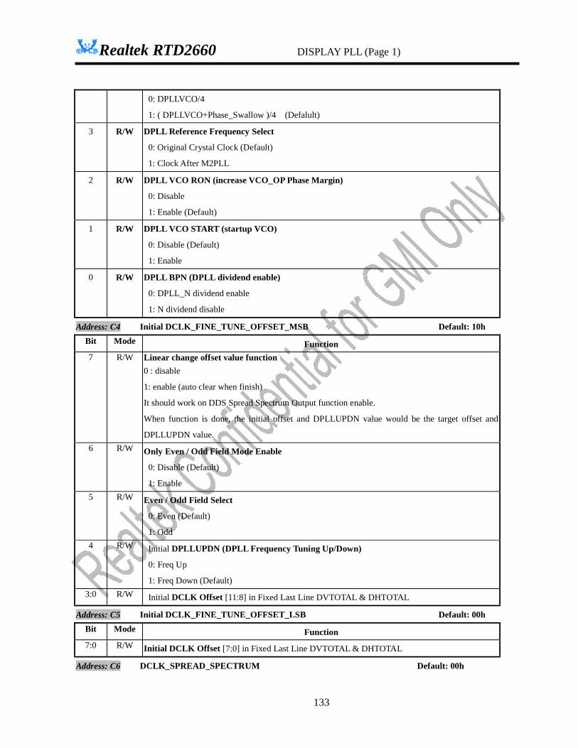
Realtek RTD2660 DISPLAY PLL (Page 1)
133
0: DPLLVCO/4
1: ( DPLLVCO+Phase_Swallow )/4 (Defalult)
3 R/W DPLL Reference Frequency Select
0: Original Crystal Clock (Default)
1: Clock After M2PLL
2 R/W DPLL VCO RON (increase VCO_OP Phase Margin)
0: Disable
1: Enable (Default)
1 R/W DPLL VCO START (startup VCO)
0: Disable (Default)
1: Enable
0 R/W DPLL BPN (DPLL dividend enable)
0: DPLL_N dividend enable
1: N dividend disable
Address: C4 Initial DCLK_FINE_TUNE_OFFSET_MSB Default: 10h Bit Mode Function 7 R/W Linear change offset value function
0 : disable
1: enable (auto clear when finish)
It should work on DDS Spread Spectrum Output function enable.
When function is done, the initial offset and DPLLUPDN value would be the target offset and
DPLLUPDN value. 6 R/W Only Even / Odd Field Mode Enable
0: Disable (Default)
1: Enable 5 R/W Even / Odd Field Select
0: Even (Default)
1: Odd 4 R/W Initial DPLLUPDN (DPLL Frequency Tuning Up/Down)
0: Freq Up
1: Freq Down (Default) 3:0 R/W Initial DCLK Offset [11:8] in Fixed Last Line DVTOTAL & DHTOTAL
Address: C5 Initial DCLK_FINE_TUNE_OFFSET_LSB Default: 00h Bit Mode Function 7:0 R/W Initial DCLK Offset [7:0] in Fixed Last Line DVTOTAL & DHTOTAL
Address: C6 DCLK_SPREAD_SPECTRUM Default: 00h
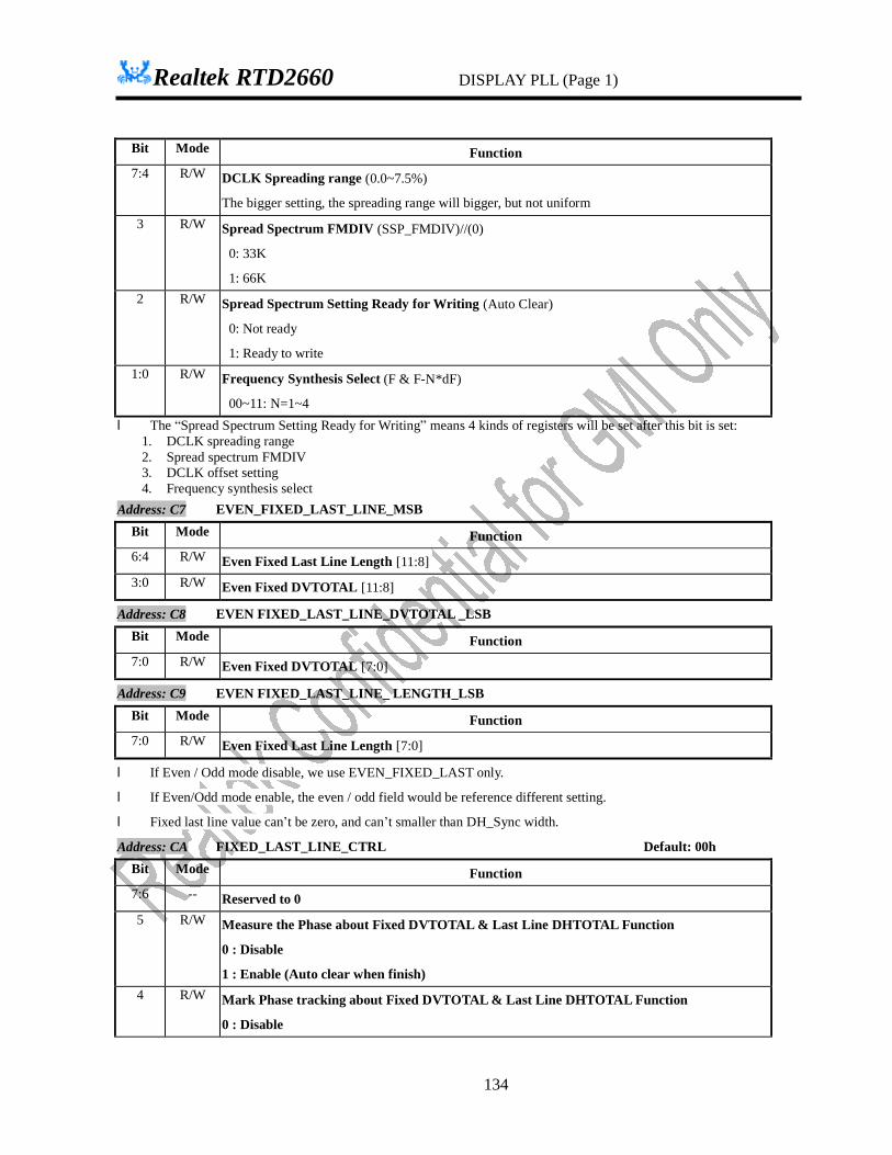
Realtek RTD2660 DISPLAY PLL (Page 1)
134
Bit Mode Function 7:4 R/W DCLK Spreading range (0.0~7.5%)
The bigger setting, the spreading range will bigger, but not uniform 3 R/W Spread Spectrum FMDIV (SSP_FMDIV)//(0)
0: 33K
1: 66K 2 R/W Spread Spectrum Setting Ready for Writing (Auto Clear)
0: Not ready
1: Ready to write 1:0 R/W Frequency Synthesis Select (F & F-N*dF)
00~11: N=1~4 l The “Spread Spectrum Setting Ready for Writing” means 4 kinds of registers will be set after this bit is set:
1. DCLK spreading range 2. Spread spectrum FMDIV 3. DCLK offset setting 4. Frequency synthesis select
Address: C7 EVEN_FIXED_LAST_LINE_MSB Bit Mode Function 6:4 R/W Even Fixed Last Line Length [11:8] 3:0 R/W Even Fixed DVTOTAL [11:8]
Address: C8 EVEN FIXED_LAST_LINE_DVTOTAL _LSB Bit Mode Function 7:0 R/W Even Fixed DVTOTAL [7:0]
Address: C9 EVEN FIXED_LAST_LINE_ LENGTH_LSB Bit Mode Function 7:0 R/W Even Fixed Last Line Length [7:0]
l If Even / Odd mode disable, we use EVEN_FIXED_LAST only.
l If Even/Odd mode enable, the even / odd field would be reference different setting.
l Fixed last line value can’t be zero, and can’t smaller than DH_Sync width.
Address: CA FIXED_LAST_LINE_CTRL Default: 00h Bit Mode Function 7:6 -- Reserved to 0 5 R/W Measure the Phase about Fixed DVTOTAL & Last Line DHTOTAL Function
0 : Disable
1 : Enable (Auto clear when finish) 4 R/W Mark Phase tracking about Fixed DVTOTAL & Last Line DHTOTAL Function
0 : Disable

Realtek RTD2660 DISPLAY PLL (Page 1)
135
1 : Enable 3 R/W Enable New Design Function in Fixed Last Line Mode
0: Disable (Default)
1: Enable 2 R/W DDS Spread Spectrum Test Enable
0: Disable (Default)
1: Enable 1 R/W Enable the Fixed DVTOTAL & Last Line DHTOTAL Function
0: Disable (Default)
1: Enable 0 R/W Enable DDS Spread Spectrum Output Function
0: Disable (Default)
1: Enable
Address: CB ODD_FIXED_LAST_LINE_MSB Bit Mode Function 6:4 R/W ODD Fixed Last Line Length [11:8] 3:0 R/W ODD Fixed DVTOTAL [11:8]
Address: CC ODD_FIXED_LAST_LINE_DVTOTAL _LSB Bit Mode Function 7:0 R/W ODD Fixed DVTOTAL [7:0]
Address: CD ODD_FIXED_LAST_LINE_ LENGTH_LSB Bit Mode Function 7:0 R/W ODD Fixed Last Line Length [7:0]
Address: CE DCLK_SPREAD_SPECTRUM Default: 00h Bit Mode Function 7:2 R/W Reserve 1 R Fixed Last Line Tracking time hit Field one
0 : hit field zero (If field zero is odd à hit odd field)
1: hit field one (If field one is even à hit even field) 0 R IVS Lead/Lag to DVS
0 : Lag
1 : Lead
Address: CF PHASE_RESULT_MSB Bit Mode Function 6:4 R Phase Line [11:8]

Realtek RTD2660 MULTIPLY PLL (Page 1)
136
3:0 R Phase Pixel [11:8]
Address: D0 PHASE_LINE_LSB Bit Mode Function 7:0 R Lead Phase Line [7:0]
Address: D1 PHASE_PIXEL_LSB Bit Mode Function
7:0 R Lead Phase Pixel [7:0]
Address: D2 Target DCLK_FINE_TUNE_OFFSET_MSB Default: 10h Bit Mode Function 7:5 R/W Reserve to 0 4 R/W Target DPLLUPDN (DPLL Frequency Tuning Up/Down)
0: Freq Up
1: Freq Down (Default) 3:0 R/W Target DCLK Offset [11:8] in Fixed Last Line DVTOTAL & DHTOTAL
Address: D3 Target DCLK_FINE_TUNE_OFFSET_LSB Default: 00h Bit Mode Function 7:0 R/W Target DCLK Offset [7:0] in Fixed Last Line DVTOTAL & DHTOTAL
Address 0xD4~0xDF are reserved
MULTIPLY PLL (Page 1) Address: E0 MULTI_PLL_CTRL0 Default: 82h
Bit Mode Function
7:3 R/W M2PLL M Code[4:0]-2 (DPM)
Default = 18 => 10000`b
2 R/W M2PLL Output Freeze
0: Normal (Default)
1: Freeze
i.e.: when output is frozen, the internal PLL is still operating
1 R/W M2PLL N Code
0: N=1
1: N=2 (Default)
0 R M2PLL WD Status
0: Normal
1: Abnormal Address: E1 MULTI_PLL_CTRL1 Default: 94h
Bit Mode Function

Realtek RTD2660 MULTIPLY PLL (Page 1)
137
7:6 R/W M2PLL Loop Filter Resistor Control
00: 15K
01: 18K
10: 21K (Default)
11: 24K
5:4 R/W M2PLL Loop Filter Charge Current Control (Default:01)
Icp=5uA+5uA*bit[4]+10uA*bit[5]
i.e.: Keep Icp/M =15u/8
3:2 R/W M2PLL WD Voltage
00: 0.80V
01: 1.0V (Default)
10: 1.2V
11: 1.4V
1 R/W M2PLL_WDRST
0: Normal (Default)
1: Reset (M2PLL Function as a Normal PLL, regardless WD)
0 R/W M2PLL_WDSET
0: Normal (Default)
1: Set (Free-Run by WD asserts VCO Voltage)
CRE2~E3 are not controlled by software reset.
Address: E4 M2PLL power down deafult:0x01 Bit Mode Function
7:1 --- Reserved
0 R/W M2PLL Power Down
0: Normal Run (Default)
1: Power Down
Address 0xE5~0xE9 are reserved
PLL27X Register::PLL CHARGE PUMP CURRENT 0XEA
Name Bit R/W Default Description Config
PLL27X_IP[1:0]
7:6
R/W 00
Charge pump current control l00:20uA, 01:30uA, 10:40uA, 11:50uA
PLL27X_RS[2:0] 5:3 R/W 011 Loop filter resistor control

Realtek RTD2660 MULTIPLY PLL (Page 1)
138
PLL27X_CS[2:0] 2:0 R/W 011 Loop filter capacitor control000:27pF, 001:33.8pF, 010:40.6pF, 011:47.4pF 100:47.4pF, 101:54.2pF, 110:61pF, 111:67.8pF
Register:: Loop filter capacitor 0XEB
Name Bit R/W Default Description Config
PLL27X_CP[2:0] 7:5
R/W 110
Loop filter capacitor control 000:1.2pF, 001:1.43pF, 010:1.65pF, 011:1.88Pf 100:2.11pF, 101:2.34pF, 110:2.57pF, 111:2.8pF
PLL27X_EN 4 R/W 0 PLL enable control, high enable
PLL27X_VCOT 3 R/W
1 VCO test mode control, 0: test mode 1: norml
PLL27x_reset_n 2 R/W
1 0: Reset pll27x 1: normal run
Rev 1:0 --- --- Reserved
Register:: PLL test mode control 0XEC
Name Bit R/W Default Description Config
PLL27X_TST[4:0]
7:3 R/W 01111 PLL test mode control
Rev 2:0 --- --- Reserved
Address 0xED~0xEF are reserved Address 0x72~0xFF are reserved

Realtek RTD2660 De-interlace(Page 6)
139
Reserved Page3~page5 De-interlace(Page 6) Register:: enable and bist control 0xA0
Name Bits Read/ Write
Reset State Comments Config
Rev 7:5 --- Reserved
ne_en 4 R/W 0x0 Noise Estimation enable
0: Not Enable,
1: Enable,
di_en 3 R/W 0x0 Deinterlace enble 0: Not Enable, 1: Enable,
BIST_MODE 2 R/W 0x0 Bist enable 0: Not Enable, 1: Enable
BIST_DONE 1 R 0x0 BIST DONE 0 : not Done 1 : Done
BIST_FAIL_0 0 R 0x0 BIST TEST FAIL 0 when BIST_DONE 1: Success 1 when BIST_DONE 1: Fail
1.2 Interpolation Control Register::Interpolation_control 0xA1
Name Bits Read/ Write
Reset State Comments Config
Rev 7:2 --- Reserved interp_range 2:0 R/W 0x3 Interpolation range
000:1 pixel 001:3 pixel 010:5 pixel 011:7 pixel 100~111:9 pixel
1.3 Intra-Field Interpolation Thresholds (Low Angle) Register:: Pixel_difference_threshold 0xA2
Name Bits Read/ Write
Reset State Comments Config
la_th1 [7:0] R/W 0x50 Pixel Difference Threshold (default : 0101 0000) Register:: Pixel_reference_difference_threshold 0xA3
Name Bits Read/ Write
Reset State Comments Config
la_th2 [7:0] R/W 0x1e Pixel Reference Difference Threshold (default : 0001 1110)
Register:: Gradient_threshold_positive 0xA4
Name Bits Read/ Reset Comments Config
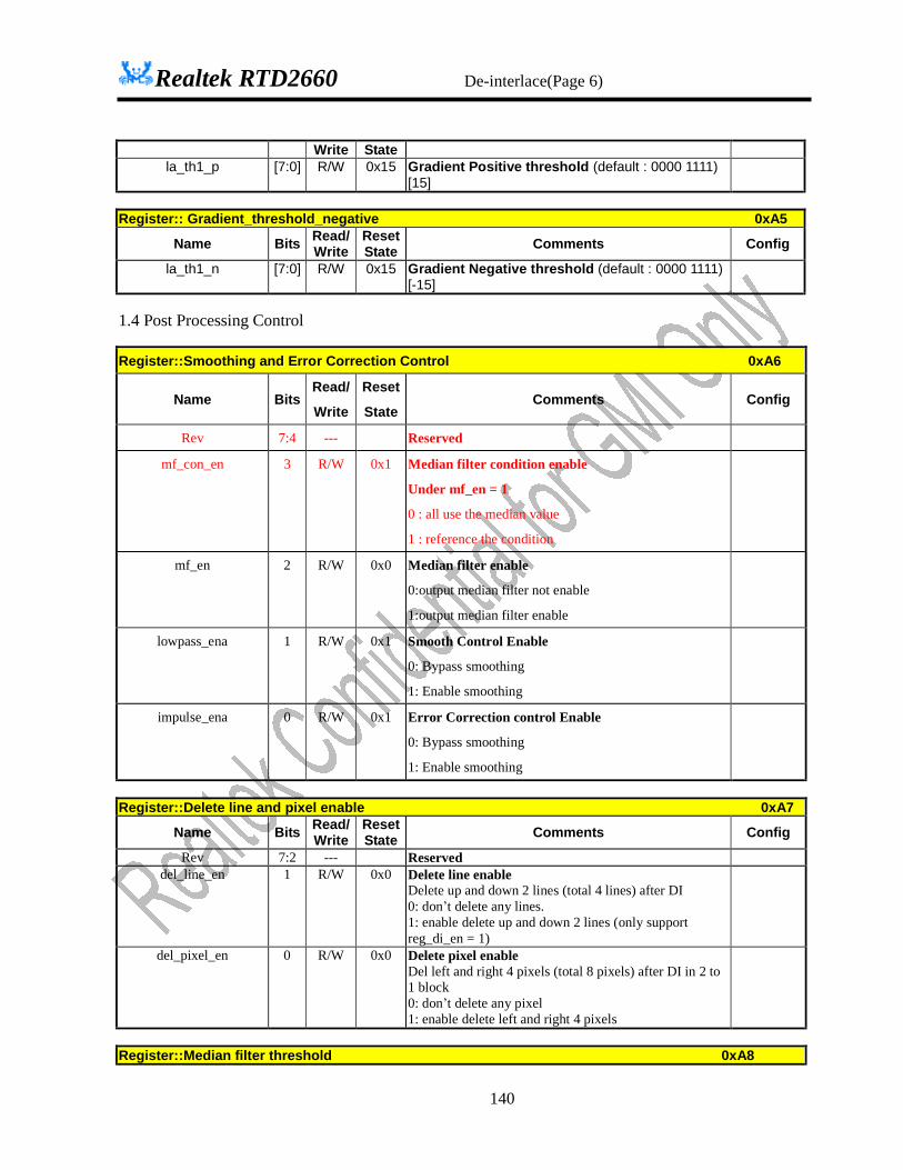
Realtek RTD2660 De-interlace(Page 6)
140
Write State la_th1_p [7:0] R/W 0x15 Gradient Positive threshold (default : 0000 1111)
[15]
Register:: Gradient_threshold_negative 0xA5
Name Bits Read/ Write
Reset State Comments Config
la_th1_n [7:0] R/W 0x15 Gradient Negative threshold (default : 0000 1111) [-15]
1.4 Post Processing Control
Register::Smoothing and Error Correction Control 0xA6
Name Bits Read/
Write
Reset
State Comments Config
Rev 7:4 --- Reserved
mf_con_en 3 R/W 0x1 Median filter condition enable
Under mf_en = 1
0 : all use the median value
1 : reference the condition
mf_en 2 R/W 0x0 Median filter enable
0:output median filter not enable
1:output median filter enable
lowpass_ena 1 R/W 0x1 Smooth Control Enable
0: Bypass smoothing
1: Enable smoothing
impulse_ena 0 R/W 0x1 Error Correction control Enable
0: Bypass smoothing
1: Enable smoothing
Register::Delete line and pixel enable 0xA7
Name Bits Read/ Write
Reset State Comments Config
Rev 7:2 --- Reserved del_line_en 1 R/W 0x0 Delete line enable
Delete up and down 2 lines (total 4 lines) after DI 0: don’t delete any lines. 1: enable delete up and down 2 lines (only support reg_di_en = 1)
del_pixel_en 0 R/W 0x0 Delete pixel enable Del left and right 4 pixels (total 8 pixels) after DI in 2 to 1 block 0: don’t delete any pixel 1: enable delete left and right 4 pixels
Register::Median filter threshold 0xA8

Realtek RTD2660 Noise Estimation(Page 6)
141
Name Bits Read/ Write
Reset State Comments Config
Mf_th 7:0 R/W 0x0A Median filter threshold Noise Estimation(Page 6) 1.Input parameter Register:: Horizontal active size (MSB) 0xA9
Name Bits Read/ Write
Reset State Comments Config
reserved_dummy 7:3 R/W 0 reserved_dummy hsize[10:8] 2:0 R/W 0x2 hsize[10:8] (MSB)
Horizotal Actve Window Size Noise Estimation Horizontal Active Window Size (width)
Register:: Horizontal active size (LSB) 0xAA
Name Bits Read/ Write
Reset State Comments Config
hsize[7:0] 7:0 R/W 0xd0 hsize[7:0] (LSB) Horizotal Actve Window Size Noise Estimation Horizontal Active Window Size (width) hsize[10:0] default : 11’d720
Register:: Vertical active size (MSB) 0xAB
Name Bits Read/ Write
Reset State Comments Config
reserved_dummy 7:3 R/W 0 reserved_dummy vsize[10:8] 2:0 R/W 0x0 vsize[10:8] (MSB)
Vertical Actve Window Size Noise Estimation Vertical Active Window Size (height)
Register:: Vertical active size (LSB) 0xAC
Name Bits Read/ Write
Reset State Comments Config
vsize[7:0] 7:0 R/W 0xf0 vsize[7:0] (LSB) Vertical Actve Window Size Noise Estimation Vertical Active Window Size (height) vsize[10:0] default : 11’d240
2 Noise Estimation calculated region Control Register:: Calculated Region Control 0xAD
Name Bits Read/ Write
Reset State Comments Config
reserved_dummy 7:4 R/W 0 reserved_dummy h_ne _region 3:2 R/W 0x3 Horizontal Noise Estimation Region
00: hactive region. 01: hactive region without 16 point front part and 16 points end part. 10: hactive region without 32 point front part and 32 points end part.
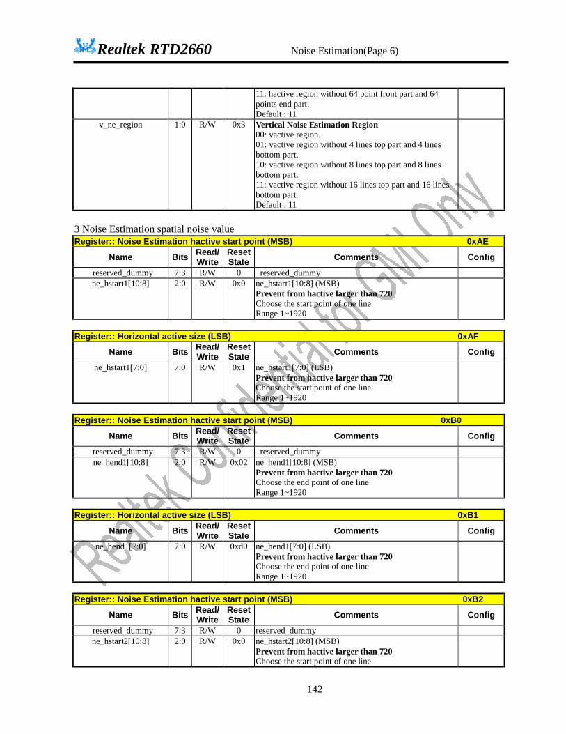
Realtek RTD2660 Noise Estimation(Page 6)
142
11: hactive region without 64 point front part and 64 points end part. Default : 11
v_ne_region 1:0 R/W 0x3 Vertical Noise Estimation Region 00: vactive region. 01: vactive region without 4 lines top part and 4 lines bottom part. 10: vactive region without 8 lines top part and 8 lines bottom part. 11: vactive region without 16 lines top part and 16 lines bottom part. Default : 11
3 Noise Estimation spatial noise value Register:: Noise Estimation hactive start point (MSB) 0xAE
Name Bits Read/ Write
Reset State Comments Config
reserved_dummy 7:3 R/W 0 reserved_dummy ne_hstart1[10:8] 2:0 R/W 0x0 ne_hstart1[10:8] (MSB)
Prevent from hactive larger than 720 Choose the start point of one line Range 1~1920
Register:: Horizontal active size (LSB) 0xAF
Name Bits Read/ Write
Reset State Comments Config
ne_hstart1[7:0] 7:0 R/W 0x1 ne_hstart1[7:0] (LSB) Prevent from hactive larger than 720 Choose the start point of one line Range 1~1920
Register:: Noise Estimation hactive start point (MSB) 0xB0
Name Bits Read/ Write
Reset State Comments Config
reserved_dummy 7:3 R/W 0 reserved_dummy ne_hend1[10:8] 2:0 R/W 0x02 ne_hend1[10:8] (MSB)
Prevent from hactive larger than 720 Choose the end point of one line Range 1~1920
Register:: Horizontal active size (LSB) 0xB1
Name Bits Read/ Write
Reset State Comments Config
ne_hend1[7:0] 7:0 R/W 0xd0 ne_hend1[7:0] (LSB) Prevent from hactive larger than 720 Choose the end point of one line Range 1~1920
Register:: Noise Estimation hactive start point (MSB) 0xB2
Name Bits Read/ Write
Reset State Comments Config
reserved_dummy 7:3 R/W 0 reserved_dummy ne_hstart2[10:8] 2:0 R/W 0x0 ne_hstart2[10:8] (MSB)
Prevent from hactive larger than 720 Choose the start point of one line
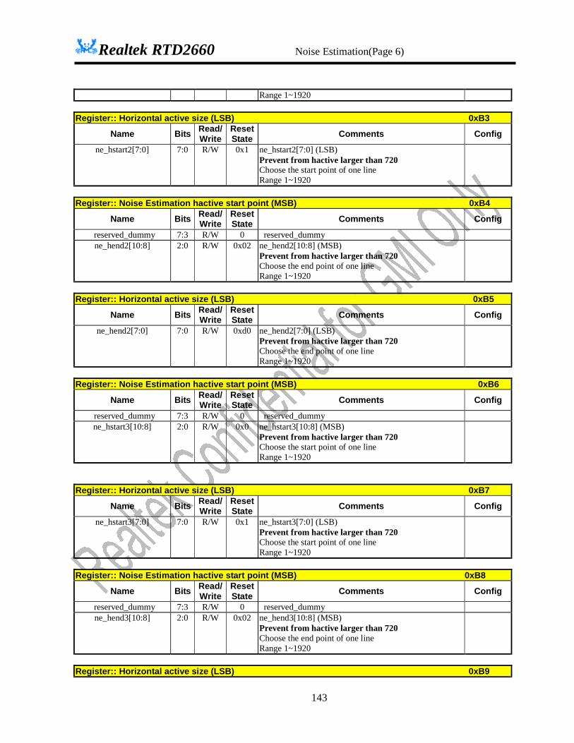
Realtek RTD2660 Noise Estimation(Page 6)
143
Range 1~1920 Register:: Horizontal active size (LSB) 0xB3
Name Bits Read/ Write
Reset State Comments Config
ne_hstart2[7:0] 7:0 R/W 0x1 ne_hstart2[7:0] (LSB) Prevent from hactive larger than 720 Choose the start point of one line Range 1~1920
Register:: Noise Estimation hactive start point (MSB) 0xB4
Name Bits Read/ Write
Reset State Comments Config
reserved_dummy 7:3 R/W 0 reserved_dummy ne_hend2[10:8] 2:0 R/W 0x02 ne_hend2[10:8] (MSB)
Prevent from hactive larger than 720 Choose the end point of one line Range 1~1920
Register:: Horizontal active size (LSB) 0xB5
Name Bits Read/ Write
Reset State Comments Config
ne_hend2[7:0] 7:0 R/W 0xd0 ne_hend2[7:0] (LSB) Prevent from hactive larger than 720 Choose the end point of one line Range 1~1920
Register:: Noise Estimation hactive start point (MSB) 0xB6
Name Bits Read/ Write
Reset State Comments Config
reserved_dummy 7:3 R/W 0 reserved_dummy ne_hstart3[10:8] 2:0 R/W 0x0 ne_hstart3[10:8] (MSB)
Prevent from hactive larger than 720 Choose the start point of one line Range 1~1920
Register:: Horizontal active size (LSB) 0xB7
Name Bits Read/ Write
Reset State Comments Config
ne_hstart3[7:0] 7:0 R/W 0x1 ne_hstart3[7:0] (LSB) Prevent from hactive larger than 720 Choose the start point of one line Range 1~1920
Register:: Noise Estimation hactive start point (MSB) 0xB8
Name Bits Read/ Write
Reset State Comments Config
reserved_dummy 7:3 R/W 0 reserved_dummy ne_hend3[10:8] 2:0 R/W 0x02 ne_hend3[10:8] (MSB)
Prevent from hactive larger than 720 Choose the end point of one line Range 1~1920
Register:: Horizontal active size (LSB) 0xB9
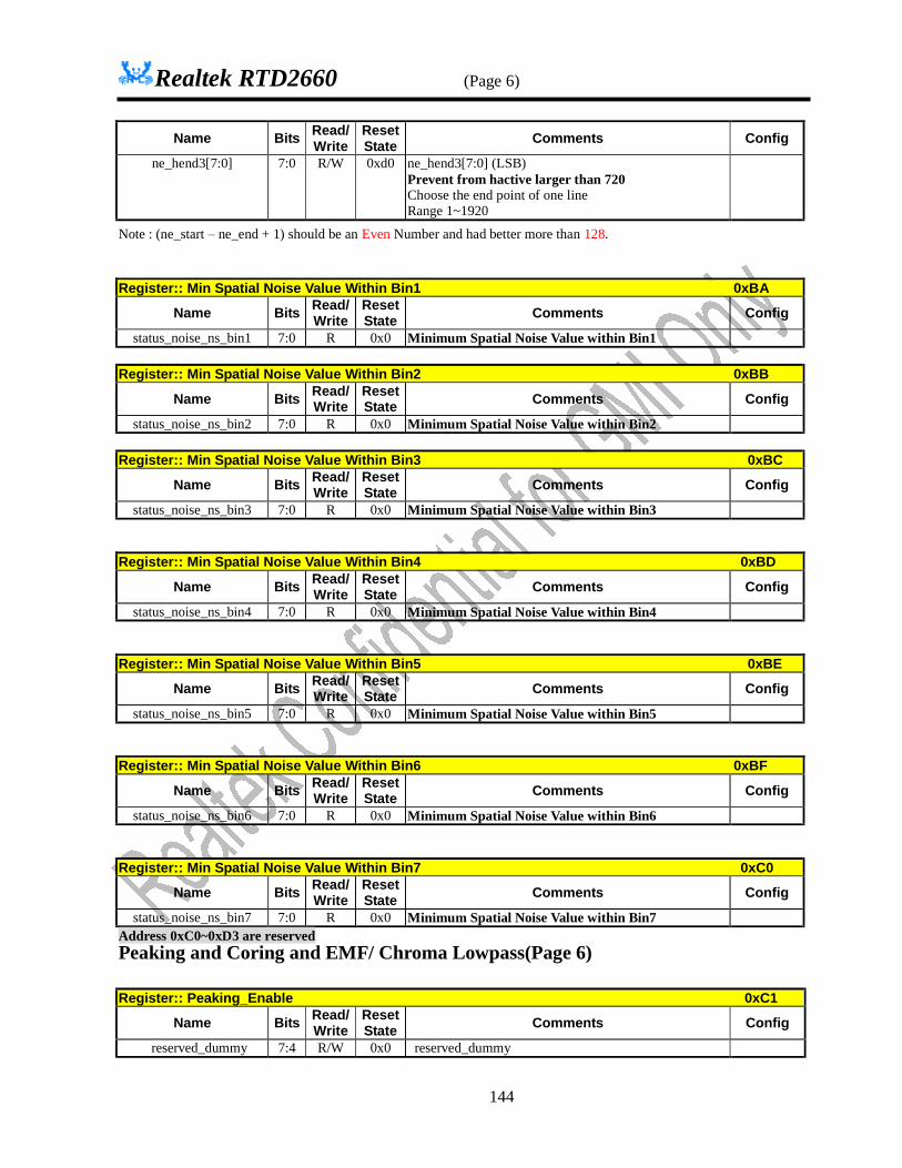
Realtek RTD2660 (Page 6)
144
Name Bits Read/ Write
Reset State Comments Config
ne_hend3[7:0] 7:0 R/W 0xd0 ne_hend3[7:0] (LSB) Prevent from hactive larger than 720 Choose the end point of one line Range 1~1920
Note : (ne_start – ne_end + 1) should be an Even Number and had better more than 128. Register:: Min Spatial Noise Value Within Bin1 0xBA
Name Bits Read/ Write
Reset State Comments Config
status_noise_ns_bin1 7:0 R 0x0 Minimum Spatial Noise Value within Bin1 Register:: Min Spatial Noise Value Within Bin2 0xBB
Name Bits Read/ Write
Reset State Comments Config
status_noise_ns_bin2 7:0 R 0x0 Minimum Spatial Noise Value within Bin2 Register:: Min Spatial Noise Value Within Bin3 0xBC
Name Bits Read/ Write
Reset State Comments Config
status_noise_ns_bin3 7:0 R 0x0 Minimum Spatial Noise Value within Bin3 Register:: Min Spatial Noise Value Within Bin4 0xBD
Name Bits Read/ Write
Reset State Comments Config
status_noise_ns_bin4 7:0 R 0x0 Minimum Spatial Noise Value within Bin4 Register:: Min Spatial Noise Value Within Bin5 0xBE
Name Bits Read/ Write
Reset State Comments Config
status_noise_ns_bin5 7:0 R 0x0 Minimum Spatial Noise Value within Bin5 Register:: Min Spatial Noise Value Within Bin6 0xBF
Name Bits Read/ Write
Reset State Comments Config
status_noise_ns_bin6 7:0 R 0x0 Minimum Spatial Noise Value within Bin6 Register:: Min Spatial Noise Value Within Bin7 0xC0
Name Bits Read/ Write
Reset State Comments Config
status_noise_ns_bin7 7:0 R 0x0 Minimum Spatial Noise Value within Bin7 Address 0xC0~0xD3 are reserved Peaking and Coring and EMF/ Chroma Lowpass(Page 6) Register:: Peaking_Enable 0xC1
Name Bits Read/Write
Reset State Comments Config
reserved_dummy 7:4 R/W 0x0 reserved_dummy

Realtek RTD2660 (Page 6)
145
pkcr_en_syn 3 R/W 0x0 Peaking and Coring Enable 0: Disable 1: Enable Valid Range: 0~1, Default Value: 0
emf_en 2 R/W 0x0 1D Extend Medain Filter Enable (when Peaking_Enable=1) 0: Disable 1: Enable Valid Range: 0~1, Default Value: 0
clp_en 1 R/W 0x0 Chroma lowpass enable 0: Disable 1: Enable Valid Range: 0~1, Default Value: 0
444_422_en 0 R/W 0x0 Color Conversion 444 to 422 enable 0: Not Enable, 1: Enable
Register:: PEAKING_DATA_00 0xC2
Name Bits Read/ Write
Reset State Comments Config
reserved_dummy 7:4 R/W 0 reserved_dummy pxl_sel 3:2 R/W 0 Peaking and Coring Horizontal Pixel Select
10:9 pixel 2*c[0]*Y[n] + c[1]*( Y[n-2] + Y[n-1] + Y[n+1] + Y[n+2] ) + c[2]*( Y[n-4] + Y[n-3] + Y[n+3] + Y[n+4] )
01:7 pixel 2*c[0]*Y[n] + c[1]*( Y[n-2] + Y[n-1] + Y[n+1] + Y[n+2] ) + c[2]*( Y[n-3] + Y[n-2] + Y[n+2] + Y[n+3] )
00:5 pixel c[0]*Y[n] + c[1]*( Y[n-1] + Y[n+1] ) + c[2]*( Y[n-2] + Y[n+2] ) Valid Range: 0~2, Default Value: 0
reg_vc_PC_Hor_PxlSel
uv_mode 1 R/W 0 444 to 422 U and V type 0 : U0 V0 U2 V2 U4 V4 …. 1 : U0 V1 U2 V3 U4 V5
C0[8] 0 R/W 0 Horizontal Peaking Filter Coefficient C0 (MSB) (C0:0-512 unsigned) Valid Range: 0~512, Default Value: 0
reg_vc_PC_Hor_Filter_C0
Register:: PEAKING_DATA_01 0xC3
Name Bits Read/ Write
Reset State Comments Config
C0[7:0] 7:0 R/W 0 Horizontal Peaking Filter Coefficient C0(LSB) (C0:0-512 unsigned) Valid Range: 0~512, Default Value: 0
reg_vc_PC_Hor_Filter_C0
Register:: PEAKING_DATA_02 0xC4
Name Bits Read/ Write
Reset State Comments Config
C1 7:0 R/W 0 Horizontal Peaking Filter Coefficient C1 (C1:-128~127 2’s Complement) Valid Range: 0~255, Default Value: 0
reg_vc_PC_Hor_Filter_C1
Register:: PEAKING_DATA_03 0xC5
Name Bits Read/ Reset Comments Config

Realtek RTD2660 (Page 6)
146
Write State C2 7:0 R/W 0 Horizontal Peaking Filter Coefficient C2
(C2:-128~127 2’s Complement) Valid Range: 0~255, Default Value: 0
reg_vc_PC_Hor_Filter_C2
Register:: PEAKING_DATA_04 0xC6
Name Bits Read/ Write
Reset State Comments Config
Gain_Blr 7:0 R/W 0 Gain Value for Low-pass at Center Range in Peaking and Coring (Gain_Blr:0/64~16/64) Valid Range: 0~255, Default Value: 0
reg_vc_PC_Gain_Blr
Register:: PEAKING_DATA_05 0xC7
Name Bits Read/ Write
Reset State Comments Config
Gain_Pos 7:0 R/W 0 Gain Value for High-pass or Band-pass at Positive Range in Peaking and Coring(Gain_Pos:0/64~255/64) Valid Range: 0~255, Default Value: 0
reg_vc_PC_Gain_Pos
Register:: PEAKING_DATA_06 0xC8
Name Bits Read/ Write
Reset State Comments Config
Gain_Neg 7:0 R/W 0 Gain Value for High-pass or Band-pass at Negative Range in Peaking and Coring(Gain_Neg:0/64~255/64) Valid Range: 0~255, Default Value: 0
reg_vc_PC_Gain_Neg
Register:: PEAKING_DATA_07 0xC9
Name Bits Read/ Write
Reset State Comments Config
reserved_dummy 7:4 R/W 0 reserved_dummy HV_Pos[9:8] 3:2 R/W 0 High Byte[9:8] of Coring High Level of Positive
Range for Peaking and Coring(HV_Pos:0~1023) Valid Range: 0~3, Default Value: 0
reg_vc_PC_HV_Pos
HV_Neg[9:8] 1:0 R/W 0 High Byte[9:8] of Coring High Level of Negative Range for Peaking and Coring(HV_Neg:0~1023) Valid Range: 0~3, Default Value: 0
reg_vc_PC_HV_Neg
Register:: PEAKING_DATA_08 0xCA
Name Bits Read/ Write
Reset State Comments Config
HV_Pos[7:0] 7:0 R/W 0 Low Byte[7:0] of Coring High Level of Positive Range for Peaking and Coring(HV_Pos:0~1023) Valid Range: 0~255, Default Value: 0
reg_vc_PC_HV_Pos
Register:: PEAKING_DATA_09 0xCB
Name Bits Read/ Write
Reset State Comments Config
HV_Neg[7:0] 7:0 R/W 0 Low Byte[7:0] of Coring High Level of Negative Range for Peaking and Coring(HV_Neg:0~1023) Valid Range: 0~255, Default Value: 0
reg_vc_PC_HV_Neg
Register:: PEAKING_DATA_0A 0xCC
Name Bits Read/ Reset Comments Config
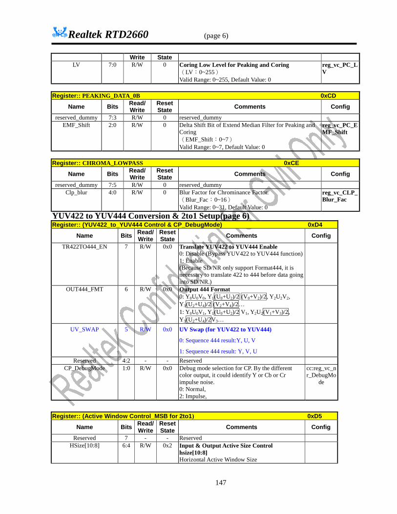
Realtek RTD2660 (page 6)
147
Write State LV 7:0 R/W 0 Coring Low Level for Peaking and Coring
(LV:0~255) Valid Range: 0~255, Default Value: 0
reg_vc_PC_LV
Register:: PEAKING_DATA_0B 0xCD
Name Bits Read/ Write
Reset State Comments Config
reserved_dummy 7:3 R/W 0 reserved_dummy EMF_Shift 2:0 R/W 0 Delta Shift Bit of Extend Median Filter for Peaking and
Coring (EMF_Shift:0~7) Valid Range: 0~7, Default Value: 0
reg_vc_PC_EMF_Shift
Register:: CHROMA_LOWPASS 0xCE
Name Bits Read/ Write
Reset State Comments Config
reserved_dummy 7:5 R/W 0 reserved_dummy Clp_blur 4:0 R/W 0 Blur Factor for Chrominance Factor.
(Blur_Fac:0~16) Valid Range: 0~31, Default Value: 0
reg_vc_CLP_Blur_Fac
YUV422 to YUV444 Conversion & 2to1 Setup(page 6) Register:: (YUV422_to_YUV444 Control & CP_DebugMode) 0xD4
Name Bits Read/Write
Reset State Comments Config
TR422TO444_EN 7 R/W 0x0 Translate YUV422 to YUV444 Enable 0: Disable (Bypass YUV422 to YUV444 function) 1: Enable (Because SD/NR only support Format444, it is necessary to translate 422 to 444 before data going into SD/NR.)
OUT444_FMT 6 R/W 0x0 Output 444 Format 0: Y0U0V0, Y1(U0+U2)/2 (V0+V2)/2, Y2U2V2, Y3(U2+U4)/2 (V2+V4)/2… 1: Y0U0V1, Y1(U0+U2)/2 V1, Y2U2(V1+V3)/2, Y3(U2+U4)/2V3…
UV_SWAP 5 R/W 0x0 UV Swap (for YUV422 to YUV444)
0: Sequence 444 result:Y, U, V
1: Sequence 444 result: Y, V, U
Reserved 4:2 - - Reserved CP_DebugMode 1:0 R/W 0x0 Debug mode selection for CP. By the different
color output, it could identify Y or Cb or Cr impulse noise. 0: Normal, 2: Impulse,
cc:reg_vc_nr_DebugMo
de
Register:: (Active Window Control_MSB for 2to1) 0xD5
Name Bits Read/Write
Reset State Comments Config
Reserved 7 - - Reserved HSize[10:8] 6:4 R/W 0x2 Input & Output Active Size Control
hsize[10:8] Horizontal Active Window Size

Realtek RTD2660 (Page 6)
148
(width)(most-significant byte). Default = 720 (dec)
Reserved 3:2 - - Reserved HBlkSize[9:8] 1:0 R/W 0x0 Input & Output Active Size Control
blanksize[9:8] Blanking Window Size (width) (least-significant byte). Default = 138 (dec)
Register:: (Active Window Control_LSB for 2to1) 0xD6
Name Bits Read/Write
Reset State Comments Config
HSize[7:0] 7:0 R/W 0xD0 Input & Output Active Size Control hsize[7:0] Horizontal Active Window Size (width) (least-significant byte). Default = 720 (dec)
Register:: (Active Window Control_LSB for 2to1) 0xD7
Name Bits Read/Write
Reset State Comments Config
HBlkSize[7:0] 7:0 R/W 0x8A Input & Output Active Size Control blanksize[7:0] Blanking Window Size (width) (least-significant byte). Default = 138 (dec)
DCTi (Dynamic Chromance Transition Improvement) in I-Domain(Page 6)
Register:: DCTi_1st_Gain 0xD8
Name Bits Read/ Write
Reset State Comments Config
En_DCTI 7 R/W 0x0 DCTI Enable 0: Disable 1: Enable (Even disable DCTI function, it still would delay 11 dummy cycles.)
Prevent_PE 6 R/W 1 Prevent Phase Error Mode 0: Disable 1: Enable
Reserved 5 R/W 0 Reserved Value 4:0 R/W 0A Adjust DCTi 1st Gain Value(5-bit)
Valid Range: 0~31, Default Value: 10 (8-bit)
Register:: DCTi_1st_Gain_Threshold 0xD9
Name Bits Read/ Write
Reset State Comments Config
Reserved 7:6 R/W 0 Reserved Value 5:0 R/W 1E Up and Down Limit for DCTi_ 1st_Gain Result
Value (6-bit) Valid Range: 0~64 (8-bit)

Realtek RTD2660 (Page 6)
149
Image Processor Performance (Noise Reduction in I-domain) Register Control(Page 6)
Clean PictureTM (Noise Reduction in I-domain) Overall Control
Register:: (CP_Ctrl) 0xDA
Name Bits Read/ Write
Reset State Comments Config
CP_ImpulseWindow 7:6 R/W 0x0 00: 3x3 Window 01: 5x3 Window
cc:reg_vc_nr_ImpulseW
indow CP_IResultWeight 5:3 R/W 0x7 I_out = I_out x ((ImpulseResultWeight+1)/8) +
T_out x (1- (ImpulseResultWeight+1)/8 ) cc:reg_vc_nr_ImpulseResultWeight
CP_SResultWeight 2:0 R/W 0x7 S_out = R x ((SpatialResultWeight+1)/8) + original x (1- (SpatialResultWeight +1)/8 )
cc:reg_vc_nr_SpatialResultWeight
Register:: (Spatial _Ctrl2) 0xDB
Name Bits Read/ Write
Reset State Comments Config
Reserved 7 R/W 0x0 Reserved CP_ZoranFilterSize 6 R/W 0x0 0: 11 points Zoran Filter
1: 15 points Zoran Filter cc:reg_vc_nr_ZoranFilt
erSize Reserved 5:3 R/W 0x0 Reserved
CP_SpatialEnable 2 R/W 0x1 0: Disable 1: Enable
cc:reg_vc_nr_SpatialEn
able CP_ImpulseEnable 1 R/W 0x1 0: Disable
1: Enable cc:
reg_vc_nr_ImpulseEnab
le Reserved 0 R/W 0x0 Reserved
Spatial noise reduction (Zoran Filter)
Register:: (Spatial_ThlY) 0xDC
Name Bits Read/ Write
Reset State Comments Config
CP_SpatialThlY 7:0 R/W 0x3 Spatial threshold for luma. Larger value increases the opportunity to do spatial noise reduction.
cc:reg_vc_nr_SpatialWe
ightY Register:: (Spatial_ThlC) 0xDD
Name Bits Read/ Write
Reset State Comments Config
CP_SpatialThlC 7:0 R/W 0x3 Spatial threshold for chroma. Larger value increases the opportunity to do spatial noise reduction.
cc:reg_vc_nr_SpatialWe
ightC
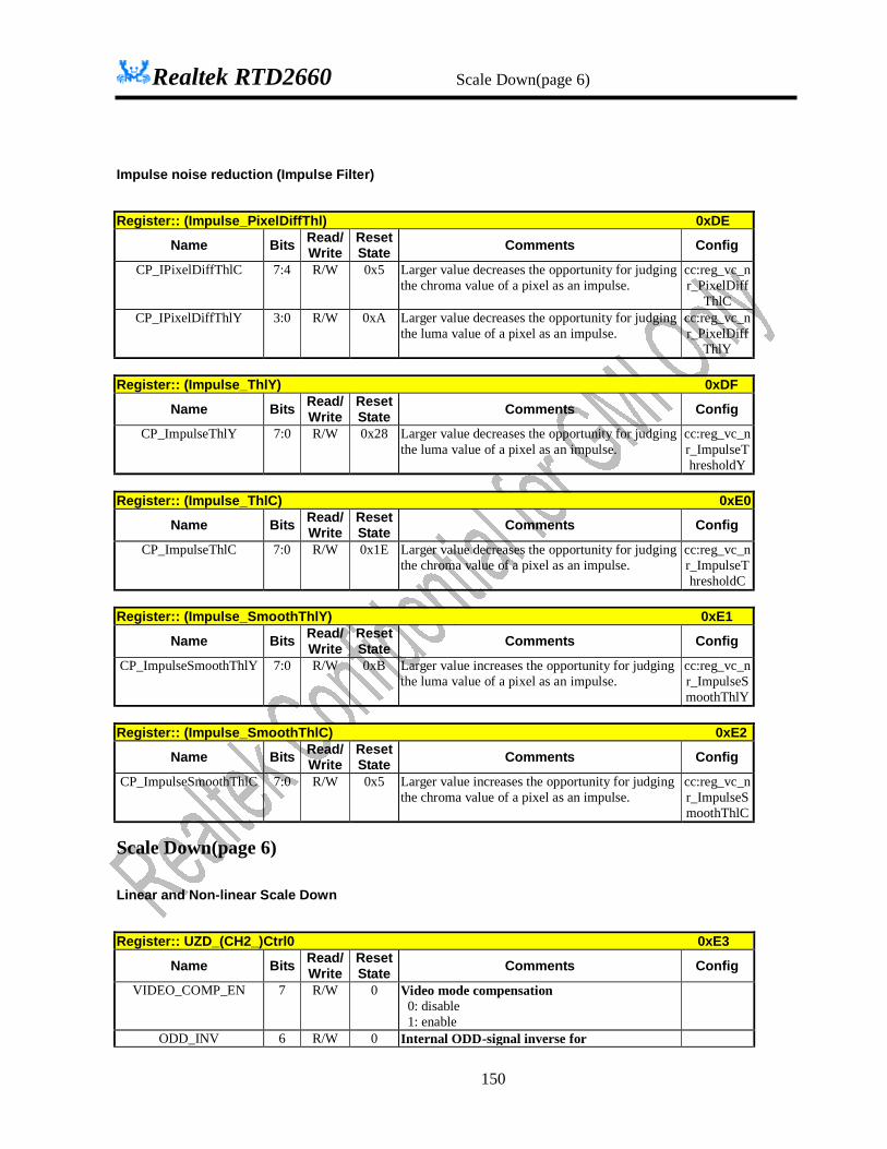
Realtek RTD2660 Scale Down(page 6)
150
Impulse noise reduction (Impulse Filter)
Register:: (Impulse_PixelDiffThl) 0xDE
Name Bits Read/ Write
Reset State Comments Config
CP_IPixelDiffThlC 7:4 R/W 0x5 Larger value decreases the opportunity for judging the chroma value of a pixel as an impulse.
cc:reg_vc_nr_PixelDiff
ThlC CP_IPixelDiffThlY 3:0 R/W 0xA Larger value decreases the opportunity for judging
the luma value of a pixel as an impulse. cc:reg_vc_nr_PixelDiff
ThlY Register:: (Impulse_ThlY) 0xDF
Name Bits Read/ Write
Reset State Comments Config
CP_ImpulseThlY 7:0 R/W 0x28 Larger value decreases the opportunity for judging the luma value of a pixel as an impulse.
cc:reg_vc_nr_ImpulseThresholdY
Register:: (Impulse_ThlC) 0xE0
Name Bits Read/ Write
Reset State Comments Config
CP_ImpulseThlC 7:0 R/W 0x1E Larger value decreases the opportunity for judging the chroma value of a pixel as an impulse.
cc:reg_vc_nr_ImpulseThresholdC
Register:: (Impulse_SmoothThlY) 0xE1
Name Bits Read/ Write
Reset State Comments Config
CP_ImpulseSmoothThlY 7:0 R/W 0xB Larger value increases the opportunity for judging the luma value of a pixel as an impulse.
cc:reg_vc_nr_ImpulseSmoothThlY
Register:: (Impulse_SmoothThlC) 0xE2
Name Bits Read/ Write
Reset State Comments Config
CP_ImpulseSmoothThlC 7:0 R/W 0x5 Larger value increases the opportunity for judging the chroma value of a pixel as an impulse.
cc:reg_vc_nr_ImpulseSmoothThlC
Scale Down(page 6)
Linear and Non-linear Scale Down
Register:: UZD_(CH2_)Ctrl0 0xE3
Name Bits Read/Write
Reset State Comments Config
VIDEO_COMP_EN 7 R/W 0 Video mode compensation 0: disable 1: enable
ODD_INV 6 R/W 0 Internal ODD-signal inverse for

Realtek RTD2660 Scale Down(page 6)
151
video-compensation 0: No invert 1: invert
CHANNEL_YUV_RGB 5 R/W 0 At boundary, there is a filter window in Noise Reduction. It needs the default value to operate this filter window. If the data channel is YUV or RGB, the default value of beyond real image sould be different. 0: YUV (black) (8bit Y:16,U:128,V:128) (10bit Y:64,U:512,V:512) 1: RGB (black) (R:0, G:0, B:0)
SBUFF_EXT 4 R/W/D 0 Short Buffer Extension Mode(Become 1920 pixel wide, 2-tap) 0: disable 1: Enable
V_TABLE_SEL 3 R/W/D 0 Select Vertical user defined filter coefficient table 0: 1st Coefficient Table 1: 2nd Coefficient Table
H_TABLE_SEL 2 R/W/D 0 Select Horizontal user defined filter coefficient table 0: 1st Coefficient Table 1: 2nd Coefficient Table
V_ZOOM_EN 1 R/W/D 0 Enable the Vertical Zoom Function 0: By pass the vertical zoom function block 1: Enable the vertical zoom function block
Cc: reg_vc_scaledown_v_zoom_en
H_ZOOM_EN 0 R/W/D 0 Enable the Horizontal Zoom Function 0: By pass the horizontal zoom function block 1: Enable the horizontal zoom function block
Cc: reg_vc_scaledown_h_zoom_en
Register:: UZD_(CH2_)Ctrl1 0xE4
Name Bits Read/Write
Reset State Comments Config
BIST_START 7 R/W 0 Line Buffer BIST Start Set 1 to start and auto-clear after finished
Reg Hw_clr
BIST_RESULT 6 R 0 Line Buffer BIST Result 0: Failed 1: Pass
DB_APPLY 5 R/W 0 UZD double buffer ready 0: Not ready to apply 1: Ready to apply Registers marked “/D” in R/W field are double buffer registers. These registers will auto-load by input VS edge. CH1 is triggered by CH1 VS, CH2 is triggered by CH2 VS.
DB_EN 4 R/W 0 UZD double buffer enable 0: Disable (Original- Write instantly by MCU write cycles) 1: Enable
BUFFER_MODE 3:2 R/W/D 0 Buffer Mode Selection 00: Bypass (Not available for both NR and vertical UZD, Horizontal UZD is available) 01: For NR (vertical UZD is not available) 10: For vertical UZD, H->V (NR is not available)
Cc: reg_vc_scaledown_buffer_mode
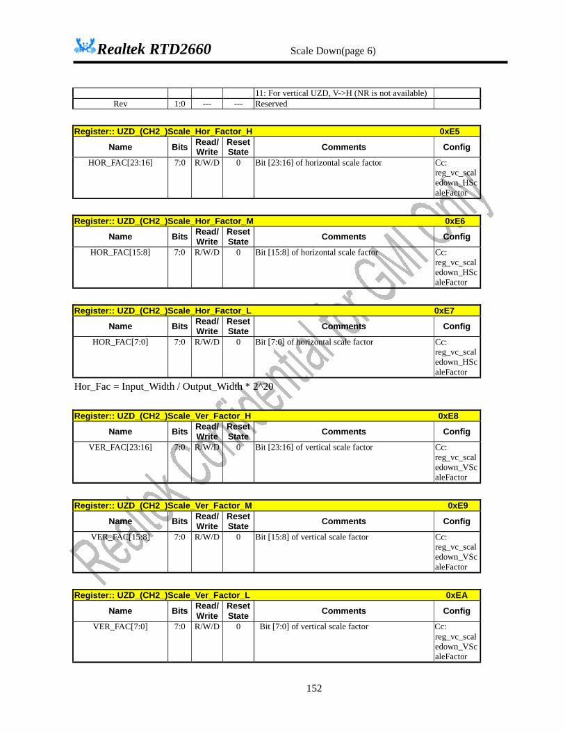
Realtek RTD2660 Scale Down(page 6)
152
11: For vertical UZD, V->H (NR is not available) Rev 1:0 --- --- Reserved
Register:: UZD_(CH2_)Scale_Hor_Factor_H 0xE5
Name Bits Read/Write
Reset State Comments Config
HOR_FAC[23:16] 7:0 R/W/D 0 Bit [23:16] of horizontal scale factor Cc: reg_vc_scaledown_HScaleFactor
Register:: UZD_(CH2_)Scale_Hor_Factor_M 0xE6
Name Bits Read/Write
Reset State Comments Config
HOR_FAC[15:8] 7:0 R/W/D 0 Bit [15:8] of horizontal scale factor Cc: reg_vc_scaledown_HScaleFactor
Register:: UZD_(CH2_)Scale_Hor_Factor_L 0xE7
Name Bits Read/Write
Reset State Comments Config
HOR_FAC[7:0] 7:0 R/W/D 0 Bit [7:0] of horizontal scale factor Cc: reg_vc_scaledown_HScaleFactor
Hor_Fac = Input_Width / Output_Width * 2^20 Register:: UZD_(CH2_)Scale_Ver_Factor_H 0xE8
Name Bits Read/Write
Reset State Comments Config
VER_FAC[23:16] 7:0 R/W/D 0 Bit [23:16] of vertical scale factor Cc: reg_vc_scaledown_VScaleFactor
Register:: UZD_(CH2_)Scale_Ver_Factor_M 0xE9
Name Bits Read/Write
Reset State Comments Config
VER_FAC[15:8] 7:0 R/W/D 0 Bit [15:8] of vertical scale factor Cc: reg_vc_scaledown_VScaleFactor
Register:: UZD_(CH2_)Scale_Ver_Factor_L 0xEA
Name Bits Read/Write
Reset State Comments Config
VER_FAC[7:0] 7:0 R/W/D 0 Bit [7:0] of vertical scale factor Cc: reg_vc_scaledown_VScaleFactor
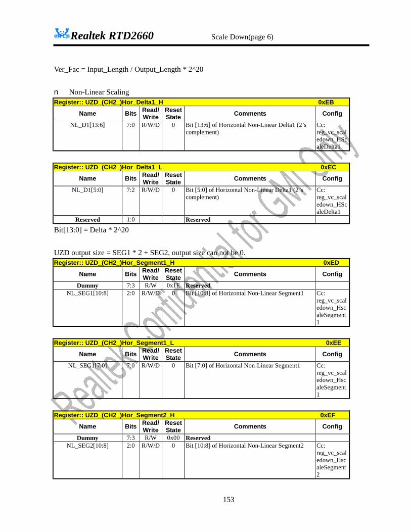
Realtek RTD2660 Scale Down(page 6)
153
Ver_Fac = Input_Length / Output_Length * 2^20 n Non-Linear Scaling Register:: UZD_(CH2_)Hor_Delta1_H 0xEB
Name Bits Read/Write
Reset State Comments Config
NL_D1[13:6] 7:0 R/W/D 0 Bit [13:6] of Horizontal Non-Linear Delta1 (2’s complement)
Cc: reg_vc_scaledown_HScaleDelta1
Register:: UZD_(CH2_)Hor_Delta1_L 0xEC
Name Bits Read/Write
Reset State Comments Config
NL_D1[5:0] 7:2 R/W/D 0 Bit [5:0] of Horizontal Non-Linear Delta1 (2’s complement)
Cc: reg_vc_scaledown_HScaleDelta1
Reserved 1:0 - - Reserved
Bit[13:0] = Delta * 2^20 UZD output size = SEG1 * 2 + SEG2, output size can not be 0. Register:: UZD_(CH2_)Hor_Segment1_H 0xED
Name Bits Read/Write
Reset State Comments Config
Dummy 7:3 R/W 0x1E Reserved NL_SEG1[10:8] 2:0 R/W/D 0 Bit [10:8] of Horizontal Non-Linear Segment1 Cc:
reg_vc_scaledown_HscaleSegment1
Register:: UZD_(CH2_)Hor_Segment1_L 0xEE
Name Bits Read/Write
Reset State Comments Config
NL_SEG1[7:0] 7:0 R/W/D 0 Bit [7:0] of Horizontal Non-Linear Segment1 Cc: reg_vc_scaledown_HscaleSegment1
Register:: UZD_(CH2_)Hor_Segment2_H 0xEF
Name Bits Read/Write
Reset State Comments Config
Dummy 7:3 R/W 0x00 Reserved NL_SEG2[10:8] 2:0 R/W/D 0 Bit [10:8] of Horizontal Non-Linear Segment2 Cc:
reg_vc_scaledown_HscaleSegment2

Realtek RTD2660 Scale Down(page 6)
154
Register:: UZD_(CH2_)Hor_Segment2_L 0xF0
Name Bits Read/Write
Reset State Comments Config
NL_SEG2[7:0] 7:0 R/W/D 0 Bit [7:0] of Horizontal Non-Linear Segment2 Cc: reg_vc_scaledown_HscaleSegment2
Register:: UZD_(CH2_)Hor_Initial_Value 0xF1
Name Bits Read/Write
Reset State Comments Config
HOR_INI 7:0 R/W 0 Horizontal Scaling Initial Value Cc: reg_vc_scaledown_HInitValue
Register:: UZD_(CH2_)Ver_Initial_Value 0xF2
Name Bits Read/Write
Reset State Comments Config
VER_INI 7:0 R/W 0 Vertical Scaling Initial Value Cc: reg_vc_scaledown_VInitValue
n FIR Coef Ctrl Register::UZD_FIR_Coef_Index 0xF3
Name Bits Read/Write
Reset State Comments Config
COEF_CH_SEL 7 R/W 0 Select H/V User Defined Filter Coefficient Table for Access Channel 0: 1st Coefficient Table 1: 2nd Coefficient Table
Cc:
COEF_READ_EN 6 R/W 0 Coefficient Read from Coef_Port 0: Disable 1: Enable (Note: It will make FIR un-normal
while reading coefficients.)
COEF_CH_INDEX 5:0 R/W 0 Coefficient Access Port Index ( 0 ~ 63) 0: c0L; 1: c0H; 2: c1L; 3: c1H; … 14:
c7L; 15: c7H; 16: c16L; 17: c16H; 18: c17L; 19: c17H; … 30:
c23L; 31: c23H; 32: c31L; 33: c31H; 34: c30L; 35: c30H; … 46:
c24L; 47: c24H; 48: c15L; 49: c15H; 50: c14L; 51: c14H; … 62:
c8L; 63: c8H;
Cc:
Register:: UZD_FIR_Coef_Port 0xF4
Name Bits Read/Write
Reset State Comments Config
COEF_PORT 7:0 R/W 0 Access port for user defined filter coefficient table Cc:

Realtek RTD2660 Scale Down(page 6)
155
l Since the 64 taps is symmetric, we need to fill the 32-coefficient sequence into table only. The sequence are c0~c7, c16~c23, c31~c24, c15~c8. Each coefficient spends 2 cycle(Low_Byte first and then High_Byte), totally 32 * 2 cycles.
UZD_CRC_CTRL
Register:: UZD_CRC_CTR 0xF5
Name Bits Read/Write Reset
State Comments Config
reserved 7:2 - - Reserved
conti 1 R/W 0 Continuously mode
0: one time mode(after finish, the bit “start” is set to 0.)
1: Continuous mode( double buffer )
Start 0 R/W 0 CRC Control:
0: Stop or finish (Auto-stop after checked a completed
display frame)
1: Start
Reg
hw_clr
Register:: UZD_CRC_HH 0xF6
Name Bits Read/Write Reset
State Comments Config
UZD_CRC[31:24] 7:0 R 0 CRC Result: CRC[31:24]
Register:: UZD_CRC_H 0xF7
Name Bits Read/Write Reset
State Comments Config
UZD_CRC[23:16] 7:0 R 0 CRC Result: CRC[23:16]
Register:: UZD_CRC_M 0xF8
Name Bits Read/Write Reset
State Comments Config
UZD_CRC[15:8] 7:0 R 0 CRC Result: CRC[15:8]
Register:: UZD_CRC_L 0xF9
Name Bits Read/Write Reset
State Comments Config

Realtek RTD2660 Vivid color-DLTi/DCTi(Page 7)
156
UZD_CRC[7:0] 7:0 R 0 CRC Result: CRC[7:0] (total occupies 38 address) Address 0xFA~0xFF are reserved Vivid color-DLTi/DCTi(Page 7)
Register:: DLTi_DCTi Enable 0xA1
Name Bits Read/ Write
Reset State Comments Config
Enabled 7 R/W 0 DLTi enable
0: Disable 1: Enable
Enabled 6 R/W 0 DCTi enable
0: Disable 1: Enable
5:0 R/W 0 Dummy bits Register:: DLTi_HF_Threshold 0xA2
Name Bits Read/ Write
Reset State Comments Config
Enabled 7 R/W 1 Check High Frequency Line Data for skip DLTi
Process.
0: Disable 1: Enable
Value 6:0 R/W 2A Threshold Value for check high frequency data Valid Range: 0~128 (128+ ), Default Value: 42 (8-bit),
Register:: DLTi_Gain 0xA3
Name Bits Read/ Write
Reset State Comments Config
Dlti_dummy 7:4 R/W 0 Dummy bits Value 3:0 R/W 05 Adjust DLTi Gain Value(4-bit)
Valid Range: 0~15 (8-bit)
Register:: DLTi_Gain_Threshold 0xA4
Name Bits Read/ Write
Reset State Comments Config
Dlti_dummy2 7:6 R/W 0 Dummy bits Value 5:0 R/W 1E Up and Down Limit for DLTi_Gain Result Value
(6-bit) Valid Range: 0~64 (8-bit),
Register:: DLTi_Options 0xA5
Name Bits Read/ Write
Reset State Comments Config
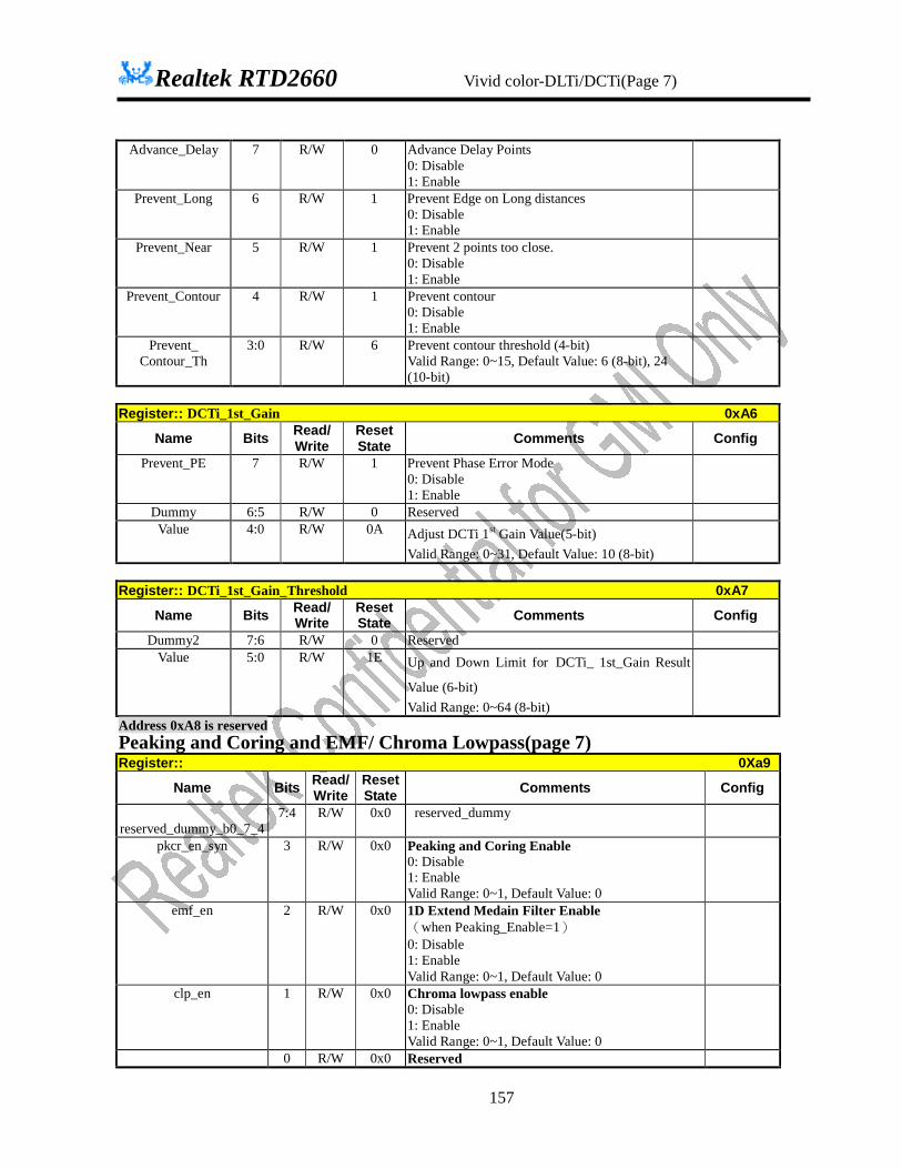
Realtek RTD2660 Vivid color-DLTi/DCTi(Page 7)
157
Advance_Delay 7 R/W 0 Advance Delay Points 0: Disable 1: Enable
Prevent_Long 6 R/W 1 Prevent Edge on Long distances 0: Disable 1: Enable
Prevent_Near 5 R/W 1 Prevent 2 points too close. 0: Disable 1: Enable
Prevent_Contour 4 R/W 1 Prevent contour 0: Disable 1: Enable
Prevent_ Contour_Th
3:0 R/W 6 Prevent contour threshold (4-bit) Valid Range: 0~15, Default Value: 6 (8-bit), 24 (10-bit)
Register:: DCTi_1st_Gain 0xA6
Name Bits Read/ Write
Reset State Comments Config
Prevent_PE 7 R/W 1 Prevent Phase Error Mode 0: Disable 1: Enable
Dummy 6:5 R/W 0 Reserved Value 4:0 R/W 0A Adjust DCTi 1st Gain Value(5-bit)
Valid Range: 0~31, Default Value: 10 (8-bit)
Register:: DCTi_1st_Gain_Threshold 0xA7
Name Bits Read/ Write
Reset State Comments Config
Dummy2 7:6 R/W 0 Reserved Value 5:0 R/W 1E Up and Down Limit for DCTi_ 1st_Gain Result
Value (6-bit) Valid Range: 0~64 (8-bit)
Address 0xA8 is reserved Peaking and Coring and EMF/ Chroma Lowpass(page 7) Register:: 0Xa9
Name Bits Read/Write
Reset State Comments Config
reserved_dummy_b0_7_4
7:4 R/W 0x0 reserved_dummy
pkcr_en_syn 3 R/W 0x0 Peaking and Coring Enable 0: Disable 1: Enable Valid Range: 0~1, Default Value: 0
emf_en 2 R/W 0x0 1D Extend Medain Filter Enable (when Peaking_Enable=1) 0: Disable 1: Enable Valid Range: 0~1, Default Value: 0
clp_en 1 R/W 0x0 Chroma lowpass enable 0: Disable 1: Enable Valid Range: 0~1, Default Value: 0
0 R/W 0x0 Reserved
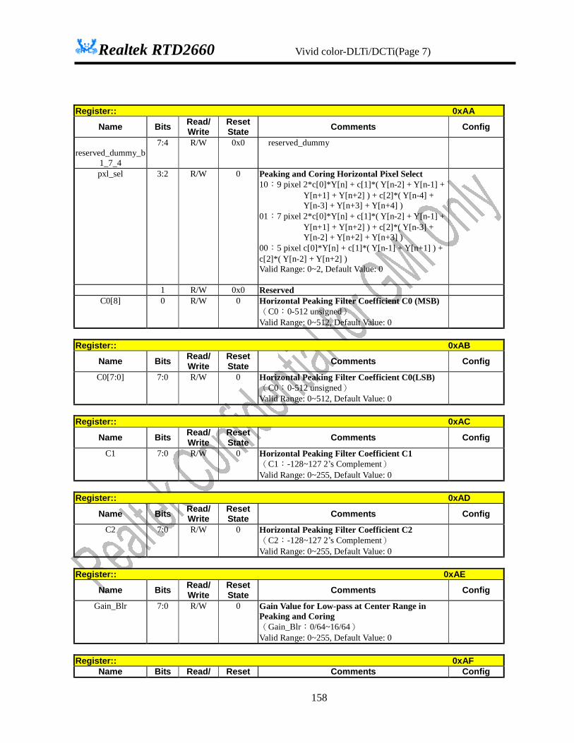
Realtek RTD2660 Vivid color-DLTi/DCTi(Page 7)
158
Register:: 0xAA
Name Bits Read/ Write
Reset State Comments Config
reserved_dummy_b
1_7_4
7:4 R/W 0x0 reserved_dummy
pxl_sel 3:2 R/W 0 Peaking and Coring Horizontal Pixel Select 10:9 pixel 2*c[0]*Y[n] + c[1]*( Y[n-2] + Y[n-1] +
Y[n+1] + Y[n+2] ) + c[2]*( Y[n-4] + Y[n-3] + Y[n+3] + Y[n+4] )
01:7 pixel 2*c[0]*Y[n] + c[1]*( Y[n-2] + Y[n-1] + Y[n+1] + Y[n+2] ) + c[2]*( Y[n-3] + Y[n-2] + Y[n+2] + Y[n+3] )
00:5 pixel c[0]*Y[n] + c[1]*( Y[n-1] + Y[n+1] ) + c[2]*( Y[n-2] + Y[n+2] ) Valid Range: 0~2, Default Value: 0
1 R/W 0x0 Reserved C0[8] 0 R/W 0 Horizontal Peaking Filter Coefficient C0 (MSB)
(C0:0-512 unsigned) Valid Range: 0~512, Default Value: 0
Register:: 0xAB
Name Bits Read/ Write
Reset State Comments Config
C0[7:0] 7:0 R/W 0 Horizontal Peaking Filter Coefficient C0(LSB) (C0:0-512 unsigned) Valid Range: 0~512, Default Value: 0
Register:: 0xAC
Name Bits Read/ Write
Reset State Comments Config
C1 7:0 R/W 0 Horizontal Peaking Filter Coefficient C1 (C1:-128~127 2’s Complement) Valid Range: 0~255, Default Value: 0
Register:: 0xAD
Name Bits Read/ Write
Reset State Comments Config
C2 7:0 R/W 0 Horizontal Peaking Filter Coefficient C2 (C2:-128~127 2’s Complement) Valid Range: 0~255, Default Value: 0
Register:: 0xAE
Name Bits Read/ Write
Reset State Comments Config
Gain_Blr 7:0 R/W 0 Gain Value for Low-pass at Center Range in Peaking and Coring (Gain_Blr:0/64~16/64) Valid Range: 0~255, Default Value: 0
Register:: 0xAF
Name Bits Read/ Reset Comments Config

Realtek RTD2660 Vivid color-DLTi/DCTi(Page 7)
159
Write State Gain_Pos 7:0 R/W 0 Gain Value for High-pass or Band-pass at
Positive Range in Peaking and Coring(Gain_Pos:0/64~255/64) Valid Range: 0~255, Default Value: 0
Register:: 0Xb0
Name Bits Read/ Write
Reset State Comments Config
Gain_Neg 7:0 R/W 0 Gain Value for High-pass or Band-pass at Negative Range in Peaking and Coring(Gain_Neg:0/64~255/64) Valid Range: 0~255, Default Value: 0
Register:: 0xb1
Name Bits Read/ Write
Reset State Comments Config
reserved_dummy_b
8_7_4
7:4 R/W 0 reserved_dummy
HV_Pos[9:8] 3:2 R/W 0 High Byte[9:8] of Coring High Level of Positive Range for Peaking and Coring(HV_Pos:0~1023) Valid Range: 0~3, Default Value: 0
HV_Neg[9:8] 1:0 R/W 0 High Byte[9:8] of Coring High Level of Negative Range for Peaking and Coring(HV_Neg:0~1023) Valid Range: 0~3, Default Value: 0
Register:: 0xb2
Name Bits Read/ Write
Reset State Comments Config
HV_Pos[7:0] 7:0 R/W 0 Low Byte[7:0] of Coring High Level of Positive Range for Peaking and Coring(HV_Pos:0~1023) Valid Range: 0~255, Default Value: 0
Register:: 0Xb3
Name Bits Read/ Write
Reset State Comments Config
HV_Neg[7:0] 7:0 R/W 0 Low Byte[7:0] of Coring High Level of Negative Range for Peaking and Coring(HV_Neg:0~1023) Valid Range: 0~255, Default Value: 0
Register:: 0xb4
Name Bits Read/ Write
Reset State Comments Config
LV 7:0 R/W 0 Coring Low Level for Peaking and Coring (LV:0~255) Valid Range: 0~255, Default Value: 0
Register:: 0xb5
Name Bits Read/ Write
Reset State Comments Config
reserved_dummy_b
c_7_3
7:3 R/W 0 reserved_dummy

Realtek RTD2660 AUTO SHARPNESS (Page 7)
160
EMF_Shift 2:0 R/W 0 Delta Shift Bit of Extend Median Filter for Peaking and Coring (EMF_Shift:0~7) Valid Range: 0~7, Default Value: 0
Register:: 0xb6
Name Bits Read/ Write
Reset State Comments Config
Reserved 7:5 -- 0 Reserved Clp_blur 4:0 R/W 0 Blur Factor for Chrominance Factor.
(Blur_Fac:0~16) Valid Range: 0~31, Default Value: 0
AUTO SHARPNESS (Page 7) Register:: AUTO_SHP_CTRL 0xB7
Name Bits Read/ Write
Reset State Comments Config
Reserved 7:1 -- 0 Reserved Reserved 1 -- 0 Reserved
Enable 0 R/W 0 Auto Sharpness Enable (It will be auto cleared after one frame summation done) 0:Disable 1:Enable Valid Range: 0~1, Default Value: 0
reg_vc_Auto_Shp_Enable
Register:: AUTO_SHP_ADDR 0xB8
Name Bits Read/ Write
Reset State Comments Config
VALUE 7:0 R/W 0 Noise Reduction and Sharpness port
address AUTO_SHP_ADDR will be increased automatically after each byte of AUTO AUTO_SHP_DATA has been accessed. Valid Range: 0~255, Default Value: 0
Register:: AUTO_SHP_DATA 0Xb9
Name Bits Read/ Write
Reset State Comments Config
Shp_data 7:0 R/W 0 DATA
Register::AUTO_SHP_DATA_00 0xb900
Name Bits Read/ Write
Reset State Comments Config
Y_LB 7:0 R/W 0 Auto Sharpness Y Range Lower Bound (Y_LB:0*2~255*2) Valid Range: 0~255, Default Value: 0
reg_vc_Auto_Shp_Y_LB
Register::AUTO_SHP_DATA_01 0xb901
Name Bits Read/ Reset Comments Config
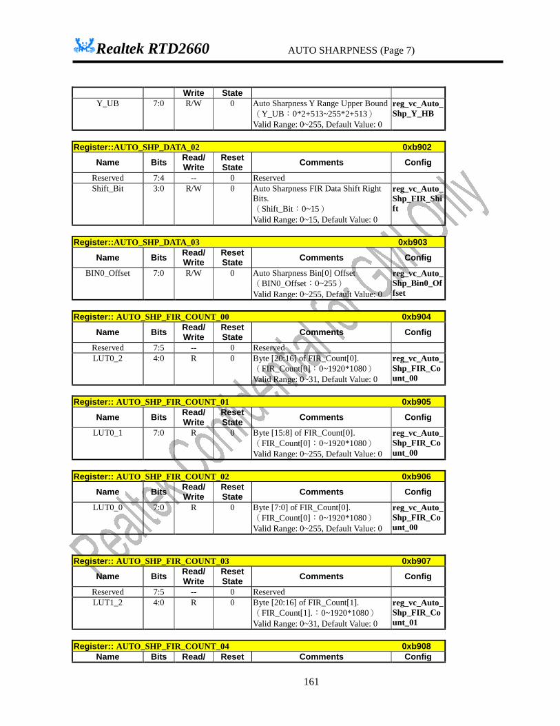
Realtek RTD2660 AUTO SHARPNESS (Page 7)
161
Write State Y_UB 7:0 R/W 0 Auto Sharpness Y Range Upper Bound
(Y_UB:0*2+513~255*2+513) Valid Range: 0~255, Default Value: 0
reg_vc_Auto_Shp_Y_HB
Register::AUTO_SHP_DATA_02 0xb902
Name Bits Read/ Write
Reset State Comments Config
Reserved 7:4 -- 0 Reserved Shift_Bit 3:0 R/W 0 Auto Sharpness FIR Data Shift Right
Bits. (Shift_Bit:0~15) Valid Range: 0~15, Default Value: 0
reg_vc_Auto_Shp_FIR_Shift
Register::AUTO_SHP_DATA_03 0xb903
Name Bits Read/ Write
Reset State Comments Config
BIN0_Offset 7:0 R/W 0 Auto Sharpness Bin[0] Offset (BIN0_Offset:0~255) Valid Range: 0~255, Default Value: 0
reg_vc_Auto_Shp_Bin0_Offset
Register:: AUTO_SHP_FIR_COUNT_00 0xb904
Name Bits Read/ Write
Reset State Comments Config
Reserved 7:5 -- 0 Reserved LUT0_2 4:0 R 0 Byte [20:16] of FIR_Count[0].
(FIR_Count[0]:0~1920*1080) Valid Range: 0~31, Default Value: 0
reg_vc_Auto_Shp_FIR_Count_00
Register:: AUTO_SHP_FIR_COUNT_01 0xb905
Name Bits Read/ Write
Reset State Comments Config
LUT0_1 7:0 R 0 Byte [15:8] of FIR_Count[0]. (FIR_Count[0]:0~1920*1080) Valid Range: 0~255, Default Value: 0
reg_vc_Auto_Shp_FIR_Count_00
Register:: AUTO_SHP_FIR_COUNT_02 0xb906
Name Bits Read/ Write
Reset State Comments Config
LUT0_0 7:0 R 0 Byte [7:0] of FIR_Count[0]. (FIR_Count[0]:0~1920*1080) Valid Range: 0~255, Default Value: 0
reg_vc_Auto_Shp_FIR_Count_00
Register:: AUTO_SHP_FIR_COUNT_03 0xb907
Name Bits Read/ Write
Reset State Comments Config
Reserved 7:5 -- 0 Reserved LUT1_2 4:0 R 0 Byte [20:16] of FIR_Count[1].
(FIR_Count[1].:0~1920*1080) Valid Range: 0~31, Default Value: 0
reg_vc_Auto_Shp_FIR_Count_01
Register:: AUTO_SHP_FIR_COUNT_04 0xb908
Name Bits Read/ Reset Comments Config
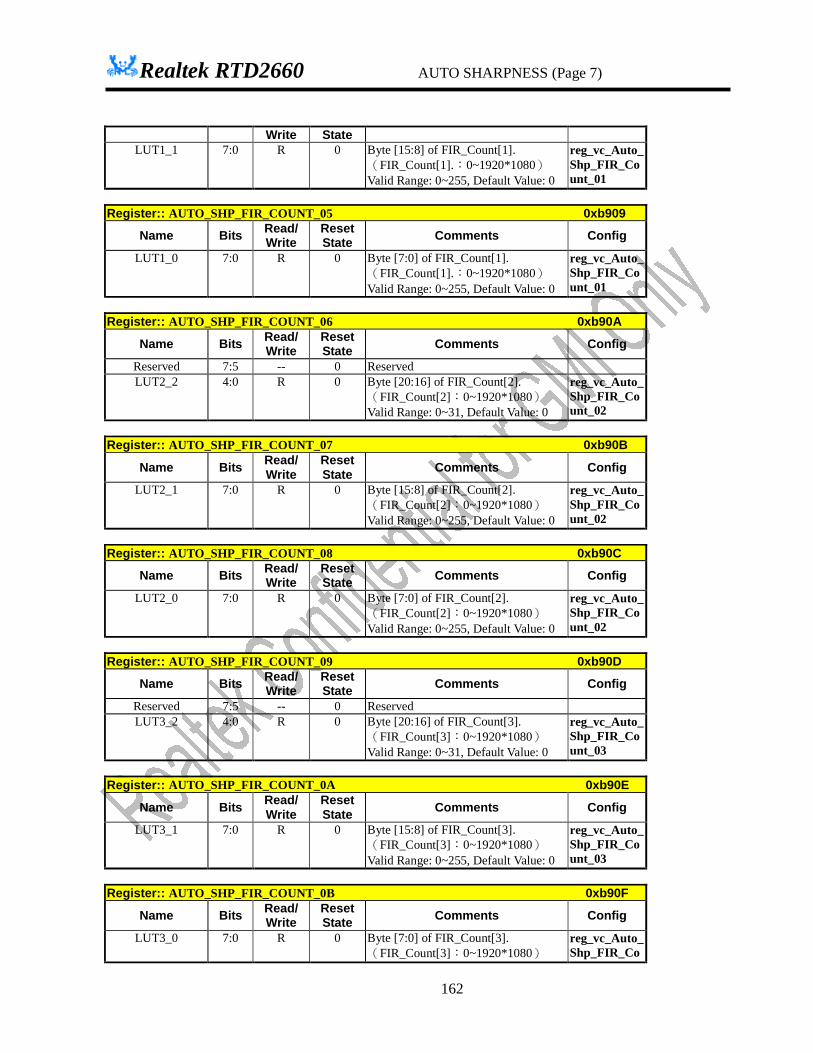
Realtek RTD2660 AUTO SHARPNESS (Page 7)
162
Write State LUT1_1 7:0 R 0 Byte [15:8] of FIR_Count[1].
(FIR_Count[1].:0~1920*1080) Valid Range: 0~255, Default Value: 0
reg_vc_Auto_Shp_FIR_Count_01
Register:: AUTO_SHP_FIR_COUNT_05 0xb909
Name Bits Read/ Write
Reset State Comments Config
LUT1_0 7:0 R 0 Byte [7:0] of FIR_Count[1]. (FIR_Count[1].:0~1920*1080) Valid Range: 0~255, Default Value: 0
reg_vc_Auto_Shp_FIR_Count_01
Register:: AUTO_SHP_FIR_COUNT_06 0xb90A
Name Bits Read/ Write
Reset State Comments Config
Reserved 7:5 -- 0 Reserved LUT2_2 4:0 R 0 Byte [20:16] of FIR_Count[2].
(FIR_Count[2]:0~1920*1080) Valid Range: 0~31, Default Value: 0
reg_vc_Auto_Shp_FIR_Count_02
Register:: AUTO_SHP_FIR_COUNT_07 0xb90B
Name Bits Read/ Write
Reset State Comments Config
LUT2_1 7:0 R 0 Byte [15:8] of FIR_Count[2]. (FIR_Count[2]:0~1920*1080) Valid Range: 0~255, Default Value: 0
reg_vc_Auto_Shp_FIR_Count_02
Register:: AUTO_SHP_FIR_COUNT_08 0xb90C
Name Bits Read/ Write
Reset State Comments Config
LUT2_0 7:0 R 0 Byte [7:0] of FIR_Count[2]. (FIR_Count[2]:0~1920*1080) Valid Range: 0~255, Default Value: 0
reg_vc_Auto_Shp_FIR_Count_02
Register:: AUTO_SHP_FIR_COUNT_09 0xb90D
Name Bits Read/ Write
Reset State Comments Config
Reserved 7:5 -- 0 Reserved LUT3_2 4:0 R 0 Byte [20:16] of FIR_Count[3].
(FIR_Count[3]:0~1920*1080) Valid Range: 0~31, Default Value: 0
reg_vc_Auto_Shp_FIR_Count_03
Register:: AUTO_SHP_FIR_COUNT_0A 0xb90E
Name Bits Read/ Write
Reset State Comments Config
LUT3_1 7:0 R 0 Byte [15:8] of FIR_Count[3]. (FIR_Count[3]:0~1920*1080) Valid Range: 0~255, Default Value: 0
reg_vc_Auto_Shp_FIR_Count_03
Register:: AUTO_SHP_FIR_COUNT_0B 0xb90F
Name Bits Read/ Write
Reset State Comments Config
LUT3_0 7:0 R 0 Byte [7:0] of FIR_Count[3]. (FIR_Count[3]:0~1920*1080)
reg_vc_Auto_Shp_FIR_Count_03
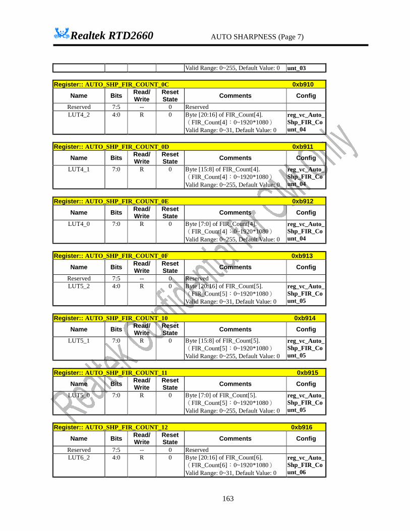
Realtek RTD2660 AUTO SHARPNESS (Page 7)
163
Valid Range: 0~255, Default Value: 0 unt_03 Register:: AUTO_SHP_FIR_COUNT_0C 0xb910
Name Bits Read/ Write
Reset State Comments Config
Reserved 7:5 -- 0 Reserved LUT4_2 4:0 R 0 Byte [20:16] of FIR_Count[4].
(FIR_Count[4]:0~1920*1080) Valid Range: 0~31, Default Value: 0
reg_vc_Auto_Shp_FIR_Count_04
Register:: AUTO_SHP_FIR_COUNT_0D 0xb911
Name Bits Read/ Write
Reset State Comments Config
LUT4_1 7:0 R 0 Byte [15:8] of FIR_Count[4]. (FIR_Count[4]:0~1920*1080) Valid Range: 0~255, Default Value: 0
reg_vc_Auto_Shp_FIR_Count_04
Register:: AUTO_SHP_FIR_COUNT_0E 0xb912
Name Bits Read/ Write
Reset State Comments Config
LUT4_0 7:0 R 0 Byte [7:0] of FIR_Count[4]. (FIR_Count[4]:0~1920*1080) Valid Range: 0~255, Default Value: 0
reg_vc_Auto_Shp_FIR_Count_04
Register:: AUTO_SHP_FIR_COUNT_0F 0xb913
Name Bits Read/ Write
Reset State Comments Config
Reserved 7:5 -- 0 Reserved LUT5_2 4:0 R 0 Byte [20:16] of FIR_Count[5].
(FIR_Count[5]:0~1920*1080) Valid Range: 0~31, Default Value: 0
reg_vc_Auto_Shp_FIR_Count_05
Register:: AUTO_SHP_FIR_COUNT_10 0xb914
Name Bits Read/ Write
Reset State Comments Config
LUT5_1 7:0 R 0 Byte [15:8] of FIR_Count[5]. (FIR_Count[5]:0~1920*1080) Valid Range: 0~255, Default Value: 0
reg_vc_Auto_Shp_FIR_Count_05
Register:: AUTO_SHP_FIR_COUNT_11 0xb915
Name Bits Read/ Write
Reset State Comments Config
LUT5_0 7:0 R 0 Byte [7:0] of FIR_Count[5]. (FIR_Count[5]:0~1920*1080) Valid Range: 0~255, Default Value: 0
reg_vc_Auto_Shp_FIR_Count_05
Register:: AUTO_SHP_FIR_COUNT_12 0xb916
Name Bits Read/ Write
Reset State Comments Config
Reserved 7:5 -- 0 Reserved LUT6_2 4:0 R 0 Byte [20:16] of FIR_Count[6].
(FIR_Count[6]:0~1920*1080) Valid Range: 0~31, Default Value: 0
reg_vc_Auto_Shp_FIR_Count_06

Realtek RTD2660 AUTO SHARPNESS (Page 7)
164
Register:: AUTO_SHP_FIR_COUNT_13 0xb917
Name Bits Read/ Write
Reset State Comments Config
LUT6_1 7:0 R 0 Byte [15:8] of FIR_Count[6]. (FIR_Count[6]:0~1920*1080) Valid Range: 0~255, Default Value: 0
reg_vc_Auto_Shp_FIR_Count_06
Register:: AUTO_SHP_FIR_COUNT_14 0xb918
Name Bits Read/ Write
Reset State Comments Config
LUT6_0 7:0 R 0 Byte [7:0] of FIR_Count[6]. (FIR_Count[6]:0~1920*1080) Valid Range: 0~255, Default Value: 0
reg_vc_Auto_Shp_FIR_Count_06
Register:: AUTO_SHP_FIR_COUNT_15 0xb919
Name Bits Read/ Write
Reset State Comments Config
Reserved 7:5 -- 0 Reserved LUT7_2 4:0 R 0 Byte [20:16] of FIR_Count[7].
(FIR_Count[7].:0~1920*1080) Valid Range: 0~31, Default Value: 0
reg_vc_Auto_Shp_FIR_Count_07
Register:: AUTO_SHP_FIR_COUNT_16 0xb91A
Name Bits Read/ Write
Reset State Comments Config
LUT7_1 7:0 R 0 Byte [15:8] of FIR_Count[7]. (FIR_Count[7].:0~1920*1080) Valid Range: 0~255, Default Value: 0
reg_vc_Auto_Shp_FIR_Count_07
Register:: AUTO_SHP_FIR_COUNT_17 0xb91B
Name Bits Read/ Write
Reset State Comments Config
LUT7_0 7:0 R 0 Byte [7:0] of FIR_Count[7]. (FIR_Count[7].:0~1920*1080) Valid Range: 0~255, Default Value: 0
reg_vc_Auto_Shp_FIR_Count_07
Register:: AUTO_SHP_FIR_COUNT_18 0xb91C
Name Bits Read/ Write
Reset State Comments Config
Reserved 7:5 -- 0 Reserved LUT8_2 4:0 R 0 Byte [20:16] of FIR_Count[8].
(FIR_Count[8]:0~1920*1080) Valid Range: 0~31, Default Value: 0
reg_vc_Auto_Shp_FIR_Count_08
Register:: AUTO_SHP_FIR_COUNT_19 0xb91D
Name Bits Read/ Write
Reset State Comments Config
LUT8_1 7:0 R 0 Byte [15:8] of FIR_Count[8]. (FIR_Count[8]:0~1920*1080) Valid Range: 0~255, Default Value: 0
reg_vc_Auto_Shp_FIR_Count_08
Register:: AUTO_SHP_FIR_COUNT_1A 0xb91E
Name Bits Read/ Write
Reset State Comments Config
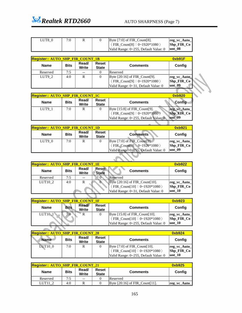
Realtek RTD2660 AUTO SHARPNESS (Page 7)
165
LUT8_0 7:0 R 0 Byte [7:0] of FIR_Count[8]. (FIR_Count[8]:0~1920*1080) Valid Range: 0~255, Default Value: 0
reg_vc_Auto_Shp_FIR_Count_08
Register:: AUTO_SHP_FIR_COUNT_1B 0xb91F
Name Bits Read/ Write
Reset State Comments Config
Reserved 7:5 -- 0 Reserved LUT9_2 4:0 R 0 Byte [20:16] of FIR_Count[9].
(FIR_Count[9]:0~1920*1080) Valid Range: 0~31, Default Value: 0
reg_vc_Auto_Shp_FIR_Count_09
Register:: AUTO_SHP_FIR_COUNT_1C 0xb920
Name Bits Read/ Write
Reset State Comments Config
LUT9_1 7:0 R 0 Byte [15:8] of FIR_Count[9]. (FIR_Count[9]:0~1920*1080) Valid Range: 0~255, Default Value: 0
reg_vc_Auto_Shp_FIR_Count_09
Register:: AUTO_SHP_FIR_COUNT_1D 0xb921
Name Bits Read/ Write
Reset State Comments Config
LUT9_0 7:0 R 0 Byte [7:0] of FIR_Count[9]. (FIR_Count[9]:0~1920*1080) Valid Range: 0~255, Default Value: 0
reg_vc_Auto_Shp_FIR_Count_09
Register:: AUTO_SHP_FIR_COUNT_1E 0xb922
Name Bits Read/ Write
Reset State Comments Config
Reserved 7:5 -- 0 Reserved LUT10_2 4:0 R 0 Byte [20:16] of FIR_Count[10].
(FIR_Count[10]:0~1920*1080) Valid Range: 0~31, Default Value: 0
reg_vc_Auto_Shp_FIR_Count_10
Register:: AUTO_SHP_FIR_COUNT_1F 0xb923
Name Bits Read/ Write
Reset State Comments Config
LUT10_1 7:0 R 0 Byte [15:8] of FIR_Count[10]. (FIR_Count[10]:0~1920*1080) Valid Range: 0~255, Default Value: 0
reg_vc_Auto_Shp_FIR_Count_10
Register:: AUTO_SHP_FIR_COUNT_20 0xb924
Name Bits Read/ Write
Reset State Comments Config
LUT10_0 7:0 R 0 Byte [7:0] of FIR_Count[10]. (FIR_Count[10]:0~1920*1080) Valid Range: 0~255, Default Value: 0
reg_vc_Auto_Shp_FIR_Count_10
Register:: AUTO_SHP_FIR_COUNT_21 0xb925
Name Bits Read/ Write
Reset State Comments Config
Reserved 7:5 -- 0 Reserved LUT11_2 4:0 R 0 Byte [20:16] of FIR_Count[11]. reg_vc_Auto_

Realtek RTD2660 AUTO SHARPNESS (Page 7)
166
(FIR_Count[11]:0~1920*1080) Valid Range: 0~31, Default Value: 0
Shp_FIR_Count_11
Register:: AUTO_SHP_FIR_COUNT_22 0xb926
Name Bits Read/ Write
Reset State Comments Config
LUT11_1 7:0 R 0 Byte [15:8] of FIR_Count[11]. (FIR_Count[11]:0~1920*1080) Valid Range: 0~255, Default Value: 0
reg_vc_Auto_Shp_FIR_Count_11
Register:: AUTO_SHP_FIR_COUNT_23 0xb927
Name Bits Read/ Write
Reset State Comments Config
LUT11_0 7:0 R 0 Byte [7:0] of FIR_Count[11]. (FIR_Count[11]:0~1920*1080) Valid Range: 0~255, Default Value: 0
reg_vc_Auto_Shp_FIR_Count_11
Register:: AUTO_SHP_FIR_COUNT_24 0xb928
Name Bits Read/ Write
Reset State Comments Config
Reserved 7:5 -- 0 Reserved LUT12_2 4:0 R 0 Byte [20:16] of FIR_Count[12].
(FIR_Count[12]:0~1920*1080) Valid Range: 0~31, Default Value: 0
reg_vc_Auto_Shp_FIR_Count_12
Register:: AUTO_SHP_FIR_COUNT_25 0xb929
Name Bits Read/ Write
Reset State Comments Config
LUT12_1 7:0 R 0 Byte [15:8] of FIR_Count[12]. (FIR_Count[12]:0~1920*1080) Valid Range: 0~255, Default Value: 0
reg_vc_Auto_Shp_FIR_Count_12
Register:: AUTO_SHP_FIR_COUNT_26 0xb92A
Name Bits Read/ Write
Reset State Comments Config
LUT12_0 7:0 R 0 Byte [7:0] of FIR_Count[12]. (FIR_Count[12]:0~1920*1080) Valid Range: 0~255, Default Value: 0
reg_vc_Auto_Shp_FIR_Count_12
Register:: AUTO_SHP_FIR_COUNT_27 0xb92B
Name Bits Read/ Write
Reset State Comments Config
Reserved 7:5 -- 0 Reserved LUT13_2 4:0 R 0 Byte [20:16] of FIR_Count[13].
(FIR_Count[13].:0~1920*1080) Valid Range: 0~31, Default Value: 0
reg_vc_Auto_Shp_FIR_Count_13
Register:: AUTO_SHP_FIR_COUNT_28 0xb92C
Name Bits Read/ Write
Reset State Comments Config
LUT13_1 7:0 R 0 Byte [15:8] of FIR_Count[13]. (FIR_Count[13].:0~1920*1080) Valid Range: 0~255, Default Value: 0
reg_vc_Auto_Shp_FIR_Count_13

Realtek RTD2660 AUTO SHARPNESS (Page 7)
167
Register:: AUTO_SHP_FIR_COUNT_29 0xb92D
Name Bits Read/ Write
Reset State Comments Config
LUT13_0 7:0 R 0 Byte [7:0] of FIR_Count[13]. (FIR_Count[13].:0~1920*1080) Valid Range: 0~255, Default Value: 0
reg_vc_Auto_Shp_FIR_Count_13
Register:: AUTO_SHP_FIR_COUNT_2A 0xb92E
Name Bits Read/ Write
Reset State Comments Config
Reserved 7:5 -- 0 Reserved LUT14_2 4:0 R 0 Byte [20:16] of FIR_Count[14].
(FIR_Count[14]:0~1920*1080) Valid Range: 0~31, Default Value: 0
reg_vc_Auto_Shp_FIR_Count_14
Register:: AUTO_SHP_FIR_COUNT_2B 0xb92F
Name Bits Read/ Write
Reset State Comments Config
LUT14_1 7:0 R 0 Byte [15:8] of FIR_Count[14]. (FIR_Count[14]:0~1920*1080) Valid Range: 0~255, Default Value: 0
reg_vc_Auto_Shp_FIR_Count_14
Register:: AUTO_SHP_FIR_COUNT_2C 0xb930
Name Bits Read/ Write
Reset State Comments Config
LUT14_0 7:0 R 0 Byte [7:0] of FIR_Count[14]. (FIR_Count[14]:0~1920*1080) Valid Range: 0~255, Default Value: 0
reg_vc_Auto_Shp_FIR_Count_14
Register:: AUTO_SHP_FIR_COUNT_2D 0xb931
Name Bits Read/ Write
Reset State Comments Config
Reserved 7:5 -- 0 Reserved LUT15_2 4:0 R 0 Byte [20:16] of FIR_Count[15].
(FIR_Count[15]:0~1920*1080) Valid Range: 0~31, Default Value: 0
reg_vc_Auto_Shp_FIR_Count_15
Register:: AUTO_SHP_FIR_COUNT_2E 0xb932
Name Bits Read/ Write
Reset State Comments Config
LUT15_1 7:0 R 0 Byte [15:8] of FIR_Count[15]. (FIR_Count[15]:0~1920*1080) Valid Range: 0~255, Default Value: 0
reg_vc_Auto_Shp_FIR_Count_15
Register:: AUTO_SHP_FIR_COUNT_2F 0xb933
Name Bits Read/ Write
Reset State Comments Config
LUT15_0 7:0 R 0 Byte [7:0] of FIR_Count[15]. (FIR_Count[15]:0~1920*1080) Valid Range: 0~255, Default Value: 0
reg_vc_Auto_Shp_FIR_Count_15
Address 0xBA~0xBE are reserved

Realtek RTD2660 Video Color Space Conversion(page 7)
168
Vivid color-Video Color Space Conversion(page 7) Register:: YUV2RGB_CTRL 0xbf
Name Bits Read/ Write
Reset State Comments Config
Dummy 7:2 R/W 0 Reserved Access 1 R/W 0 Enable YUV/RGB coefficient Access
0: Disable 1: Enable
Enable 0 R/W 0 Enable YUV to RGB Conversion 0: Disable YUV-to-RGB conversion 1: Enable YUV-to-RGB conversion
Register:: YUV2RGB_ACCESS 0xc0
Name Bits Read/ Write
Reset State Comments Config
Write_Enabled 7:4 R/W 0 YUV Coefficient Write Enable: 0000: K11 high byte
0001: K11 low byte 0010: K13 high byte 0011: K13 low byte 0100: K22 high byte
0101: K22 low byte 0110: K23 high byte 0111: K23 low byte 1000: K32 high byte 1001: K32 low byte 1010: Roffset high byte 1011: Roffset low byte 1100: Goffset high byte 1101: Goffset low byte 1110: Boffset high byte 1111: Boffset low byte
Cb_Cr_Clamp 3 R/W 0 Cb Cr Clamp 0: Bypass 1: Cb-(512<<2), Cr-(512<<2)
Y_Clamp 2 R/W 0 Y Clamp 0: Bypass 1: Y-(64<<2)
dummy2 1:0 R/W 0 Reserved Register:: YUV_RGB_COEF_DATA 0xc1
Name Bits Read/ Write
Reset State Comments Config
COEF 7:0 W - COEF_DATA[7:0] Address 0xC2~0xC6 are reserved Vivid color-DCC (Page 7) Register:: DCC_CTRL_0 0xc7
Name Bits R/W Default Comments Config
DCC_EN 7 R/W 0 DCC_ENABLE 0: Disable 1: Enable
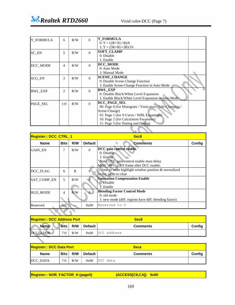
Realtek RTD2660 Vivid color-DCC (Page 7)
169
Y_FORMULA 6 R/W 0 Y_FORMULA 0: Y = (2R+5G+B)/8 1: Y = (5R+8G+3B)/16
SC_EN 5 R/W 0 SOFT_CLAMP 0: Disable 1: Enable
DCC_MODE 4 R/W 0 DCC_MODE 0: Auto Mode 1: Manual Mode
SCG_EN 3 R/W 0 SCENE_CHANGE 0: Disable Scene-Change Function 1: Enable Scene-Change Function in Auto Mode
BWL_EXP 2 R/W 0 BWL_EXP 0: Disable Black/White Level Expansion 1: Enable Black/White Level Expansion in Auto Mode
PAGE_SEL 1:0 R/W 0 DCC_PAGE_SEL 00: Page 0 (for Histogram / Ymin-max / Soft-Clamping /
Scene-Change) 01: Page 1 (for Y-Curve / WBL Expansion) 10: Page 2 (for Calculation Parameter) 11: Page 3 (for Testing and Debug)
Register:: DCC_CTRL_1 0xc8
Name Bits R/W Default Comments Config
GAIN_EN 7 R/W 0 DCC gain control enable 0: Disable 1: Enable Note: DCC gain control enable must delay
MOV_AVG_LEN frame after DCC enable.
DCC_FLAG 6 R 0 1: time to write highlight window position & normalized factor, write to clear
SAT_COMP_EN 5 R/W 0 Saturation Compensation Enable 0: Disable 1: Enable
BLD_MODE 4 R/W 0 Blending Factor Control Mode 0: old mode 1: new mode (diff. regions have diff. blending factor)
Reserved 3:0 -- 0x00 Reserved to 0
Register:: DCC Address Port 0xc9
Name Bits R/W Default Comments Config
DCC_ADDR 7:0 R/W 0x00 DCC address
Register:: DCC Data Port 0xca
Name Bits R/W Default Comments Config
DCC_DATA 7:0 R/W 0x00 DCC data
Register:: NOR_FACTOR_H (page0) (ACCESS[C9,CA]) 0x00
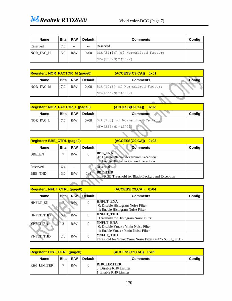
Realtek RTD2660 Vivid color-DCC (Page 7)
170
Name Bits R/W Default Comments Config
Reserved 7:6 -- -- Reserved
NOR_FAC_H 5:0 R/W 0x00 Bit[21:16] of Normalized Factor; NF=(255/N)*(2^22)
Register:: NOR_FACTOR_M (page0) (ACCESS[C9,CA]) 0x01
Name Bits R/W Default Comments Config
NOR_FAC_M 7:0 R/W 0x00 Bit[15:8] of Normalized Factor; NF=(255/N)*(2^22)
Register:: NOR_FACTOR_L (page0) (ACCESS[C9,CA]) 0x02
Name Bits R/W Default Comments Config
NOR_FAC_L 7:0 R/W 0x00 Bit[7:0] of Normalized Factor; NF=(255/N)*(2^22)
Register:: BBE_CTRL (page0) (ACCESS[C9,CA]) 0x03
Name Bits R/W Default Comments Config
BBE_EN 7 R/W 0 BBE_ENA 0: Disable Black-Background Exception 1: Enable Black-Background Exception
Reserved 6:4 -- -- Reserved
BBE_THD 3:0 R/W 0x4 BBE_THD 8-bit RGB Threshold for Black-Background Exception
Register:: NFLT_CTRL (page0) (ACCESS[C9,CA]) 0x04
Name Bits R/W Default Comments Config
HNFLT_EN 7 R/W 0 HNFLT_ENA 0: Disable Histogram Noise Filter 1: Enable Histogram Noise Filter
HNFLT_THD 6:4 R/W 0 HNFLT_THD Threshold for Histogram Noise Filter
YNFLT_EN 3 R/W 0 YNFLT_ENA 0: Disable Ymax / Ymin Noise Filter 1: Enable Ymax / Ymin Noise Filter
YNFLT_THD 2:0 R/W 0 YNFLT_THD Threshold for Ymax/Ymin Noise Filter (= 4*YNFLT_THD)
Register:: HIST_CTRL (page0) (ACCESS[C9,CA]) 0x05
Name Bits R/W Default Comments Config
RH0_LIMITER 7 R/W 0 RH0_LIMITER 0: Disable RH0 Limiter 1: Enable RH0 Limiter

Realtek RTD2660 Vivid color-DCC (Page 7)
171
RH1_LIMITER 6 R/W 0 RH1_LIMITER 0: Disable RH1 Limiter 1: Enable RH1 Limiter
REAL_MA_LEN 5:3 R -- Real MOV_AVG_LEN may be different with MOV_AVG_LEN, if SCG enable
MOV_AVG_LEN 2:0 R/W 0 MOV_AVG_LEN 000: Histogram Moving Average Length = 1 001: Histogram Moving Average Length = 2 010: Histogram Moving Average Length = 4 011: Histogram Moving Average Length = 8 100: Histogram Moving Average Length = 16 101~111: reserved
Register:: SOFT_CLAMP (page0) (ACCESS[C9,CA]) 0x06
Name Bits R/W Default Comments Config
SOFT_CLAMP 7:0 R/W 0xB0 Slope of Soft-Clamping (= SOFT_CLAMP / 256)
Register:: Y_MAX_LB (page0) (ACCESS[C9,CA]) 0x07
Name Bits R/W Default Comments Config
Y_MAX_LB 7:0 R/W 0xFF Lower Bound of Y_MAX (= 4*Y_MAX_LB)
Register:: Y_MIN_HB (page0) (ACCESS[C9,CA]) 0x08
Name Bits R/W Default Comments Config
Y_MIN_HB 7:0 R/W 0x00 Higher Bound of Y_MIN (= 4*Y_MIN_HB)
Register:: SCG_PERIOD (page0) (ACCESS[C9,CA]) 0x09
Name Bits R/W Default Comments Config
SCG_MODE 7 R/W 0 Scene-Change Control Mode 0: old mode (2553V) 1: new mode (2622)
Reserved 6:5 -- -- Reserved
SCG_PERIOD 4:0 R/W 0x10 Scene-Change Mode Period = 1~32. Note: SCG_PERIOD >= MOV_AVG_LEN,
CRED-05[2:0](page0)
Register:: SCG_LB (page0) (ACCESS[C9,CA]) 0x0A
Name Bits R/W Default Comments Config
SCG_LB 7:0 R/W 0x00 SCG_DIFF Lower Bound for Exiting Scene-Change Mode
Register:: SCG_HB (page0) (ACCESS[C9,CA]) 0x0B
Name Bits R/W Default Comments Config

Realtek RTD2660 Vivid color-DCC (Page 7)
172
SCG_HB 7:0 R/W 0xFF SCG_DIFF Higher Bound for Exiting Scene-Change Mode
Register:: POPUP_CTRL (page0) (ACCESS[C9,CA]) 0x0C
Name Bits R/W Default Comments Config
Reserved 7:1 -- -- Reserved
POPUP_BIT 0 R -- Reg[0D]~Reg[16] are updated every frame. Once POPUP_BIT is read, the value of Reg[0D] ~ Reg[16] will not be updated until Reg[16] is read.
Register:: SCG_DIFF (page0) (ACCESS[C9,CA]) 0x0D
Name Bits R/W Default Comments Config
SCG_DIFF 7:0 R -- = (Histogram Difference between Current Frame and Average) / 8
Register:: Y_MAX_VAL (page0) (ACCESS[C9,CA]) 0x0E
Name Bits R/W Default Comments Config
Y_MAX_VAL 7:0 R -- = Max { Y_MAX_LB, (Y Maximum in Current Frame / 4) }
Register:: Y_MIN_VAL (page0) (ACCESS[C9,CA]) 0x0F
Name Bits R/W Default Comments Config
Y_MIN_VAL 7:0 R -- = Min { Y_MIN_HB, (Y Minimum in Current Frame / 4) }
Register:: S0_VALUE (page0) (ACCESS[C9,CA]) 0x10
Name Bits R/W Default Comments Config
S0_VALUE 7:0 R -- Normalized Histogram S0 Value
Register:: S1_VALUE (page0) (ACCESS[C9,CA]) 0x11
Name Bits R/W Default Comments Config
S1_VALUE 7:0 R -- Normalized Histogram S1 Value
Register:: S2_VALUE (page0) (ACCESS[C9,CA]) 0x12
Name Bits R/W Default Comments Config
S2_VALUE 7:0 R -- Normalized Histogram S2 Value
Register:: S3_VALUE (page0) (ACCESS[C9,CA]) 0x13
Name Bits R/W Default Comments Config
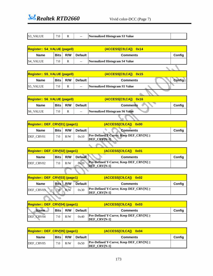
Realtek RTD2660 Vivid color-DCC (Page 7)
173
S3_VALUE 7:0 R -- Normalized Histogram S3 Value
Register:: S4_VALUE (page0) (ACCESS[C9,CA]) 0x14
Name Bits R/W Default Comments Config
S4_VALUE 7:0 R -- Normalized Histogram S4 Value
Register:: S5_VALUE (page0) (ACCESS[C9,CA]) 0x15
Name Bits R/W Default Comments Config
S5_VALUE 7:0 R -- Normalized Histogram S5 Value
Register:: S6_VALUE (page0) (ACCESS[C9,CA]) 0x16
Name Bits R/W Default Comments Config
S6_VALUE 7:0 R -- Normalized Histogram S6 Value
Register:: DEF_CRV[01] (page1) (ACCESS[C9,CA]) 0x00
Name Bits R/W Default Comments Config
DEF_CRV01 7:0 R/W 0x10 Pre-Defined Y-Curve; Keep DEF_CRV[N] ≥ DEF_CRV[N-1]
Register:: DEF_CRV[02] (page1) (ACCESS[C9,CA]) 0x01
Name Bits R/W Default Comments Config
DEF_CRV02 7:0 R/W 0x20 Pre-Defined Y-Curve; Keep DEF_CRV[N] ≥ DEF_CRV[N-1]
Register:: DEF_CRV[03] (page1) (ACCESS[C9,CA]) 0x02
Name Bits R/W Default Comments Config
DEF_CRV03 7:0 R/W 0x30 Pre-Defined Y-Curve; Keep DEF_CRV[N] ≥ DEF_CRV[N-1]
Register:: DEF_CRV[04] (page1) (ACCESS[C9,CA]) 0x03
Name Bits R/W Default Comments Config
DEF_CRV04 7:0 R/W 0x40 Pre-Defined Y-Curve; Keep DEF_CRV[N] ≥ DEF_CRV[N-1]
Register:: DEF_CRV[05] (page1) (ACCESS[C9,CA]) 0x04
Name Bits R/W Default Comments Config
DEF_CRV05 7:0 R/W 0x50 Pre-Defined Y-Curve; Keep DEF_CRV[N] ≥ DEF_CRV[N-1]

Realtek RTD2660 Vivid color-DCC (Page 7)
174
Register:: DEF_CRV[06] (page1) (ACCESS[C9,CA]) 0x05
Name Bits R/W Default Comments Config
DEF_CRV06 7:0 R/W 0x60 Pre-Defined Y-Curve; Keep DEF_CRV[N] ≥ DEF_CRV[N-1]
Register:: DEF_CRV[07] (page1) (ACCESS[C9,CA]) 0x06
Name Bits R/W Default Comments Config
DEF_CRV07 7:0 R/W 0x70 Pre-Defined Y-Curve; Keep DEF_CRV[N] ≥ DEF_CRV[N-1]
Register:: DEF_CRV[08] (page1) (ACCESS[C9,CA]) 0x07
Name Bits R/W Default Comments Config
DEF_CRV08 7:0 R/W 0x80 Pre-Defined Y-Curve; Keep DEF_CRV[N] ≥ DEF_CRV[N-1]
Register:: DEF_CRV[09] (page1) (ACCESS[C9,CA]) 0x08
Name Bits R/W Default Comments Config
DEF_CRV09 7:0 R/W 0x90 Pre-Defined Y-Curve; Keep DEF_CRV[N] ≥ DEF_CRV[N-1]
Register:: DEF_CRV[10] (page1) (ACCESS[C9,CA]) 0x09
Name Bits R/W Default Comments Config
DEF_CRV10 7:0 R/W 0xA0 Pre-Defined Y-Curve; Keep DEF_CRV[N] ≥ DEF_CRV[N-1]
Register:: DEF_CRV[11] (page1) (ACCESS[C9,CA]) 0x0A
Name Bits R/W Default Comments Config
DEF_CRV11 7:0 R/W 0xB0 Pre-Defined Y-Curve; Keep DEF_CRV[N] ≥ DEF_CRV[N-1]
Register:: DEF_CRV[12] (page1) (ACCESS[C9,CA]) 0x0B
Name Bits R/W Default Comments Config
DEF_CRV12 7:0 R/W 0xC0 Pre-Defined Y-Curve; Keep DEF_CRV[N] ≥ DEF_CRV[N-1]
Register:: DEF_CRV[13] (page1) (ACCESS[C9,CA]) 0x0C
Name Bits R/W Default Comments Config
DEF_CRV13 7:0 R/W 0xD0 Pre-Defined Y-Curve; Keep DEF_CRV[N] ≥ DEF_CRV[N-1]
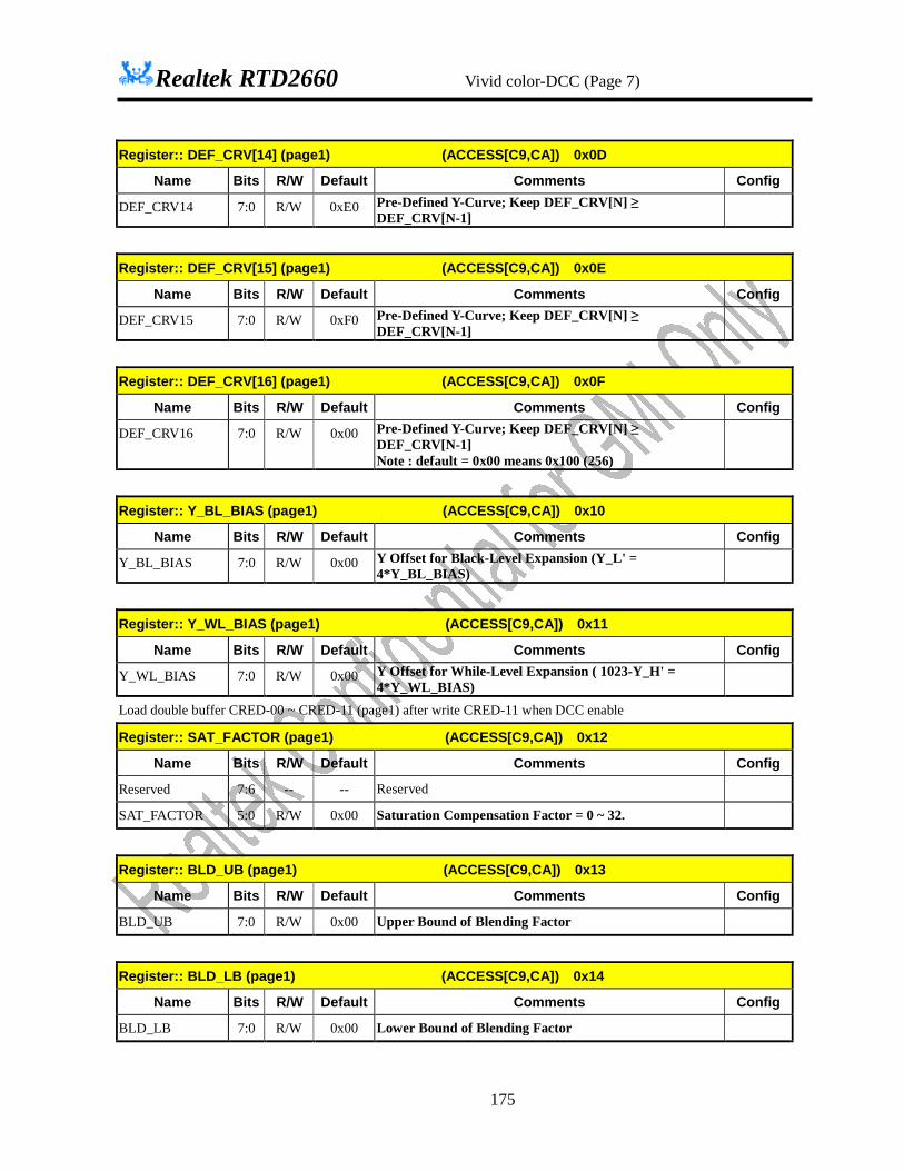
Realtek RTD2660 Vivid color-DCC (Page 7)
175
Register:: DEF_CRV[14] (page1) (ACCESS[C9,CA]) 0x0D
Name Bits R/W Default Comments Config
DEF_CRV14 7:0 R/W 0xE0 Pre-Defined Y-Curve; Keep DEF_CRV[N] ≥ DEF_CRV[N-1]
Register:: DEF_CRV[15] (page1) (ACCESS[C9,CA]) 0x0E
Name Bits R/W Default Comments Config
DEF_CRV15 7:0 R/W 0xF0 Pre-Defined Y-Curve; Keep DEF_CRV[N] ≥ DEF_CRV[N-1]
Register:: DEF_CRV[16] (page1) (ACCESS[C9,CA]) 0x0F
Name Bits R/W Default Comments Config
DEF_CRV16 7:0 R/W 0x00 Pre-Defined Y-Curve; Keep DEF_CRV[N] ≥ DEF_CRV[N-1] Note : default = 0x00 means 0x100 (256)
Register:: Y_BL_BIAS (page1) (ACCESS[C9,CA]) 0x10
Name Bits R/W Default Comments Config
Y_BL_BIAS 7:0 R/W 0x00 Y Offset for Black-Level Expansion (Y_L' = 4*Y_BL_BIAS)
Register:: Y_WL_BIAS (page1) (ACCESS[C9,CA]) 0x11
Name Bits R/W Default Comments Config
Y_WL_BIAS 7:0 R/W 0x00 Y Offset for While-Level Expansion ( 1023-Y_H' = 4*Y_WL_BIAS)
Load double buffer CRED-00 ~ CRED-11 (page1) after write CRED-11 when DCC enable
Register:: SAT_FACTOR (page1) (ACCESS[C9,CA]) 0x12
Name Bits R/W Default Comments Config
Reserved 7:6 -- -- Reserved
SAT_FACTOR 5:0 R/W 0x00 Saturation Compensation Factor = 0 ~ 32.
Register:: BLD_UB (page1) (ACCESS[C9,CA]) 0x13
Name Bits R/W Default Comments Config
BLD_UB 7:0 R/W 0x00 Upper Bound of Blending Factor
Register:: BLD_LB (page1) (ACCESS[C9,CA]) 0x14
Name Bits R/W Default Comments Config
BLD_LB 7:0 R/W 0x00 Lower Bound of Blending Factor

Realtek RTD2660 Vivid color-DCC (Page 7)
176
Register:: DEV_FACTOR (page1) (ACCESS[C9,CA]) 0x15
Name Bits R/W Default Comments Config
DEV_FACTOR 7:0 R/W 0x00 Deviation Weighting Factor
Register:: BLD_VAL_SEL (page1) (ACCESS[C9,CA]) 0x16
Name Bits R/W Default Comments Config
WL_RANGE 7:6 R/W 0x00 White-Level Range 00: Yi = 512 (Z8) 01: Yi = 576 (Z9) 10: Yi = 640 (Z10) 11: Yi = 704 (Z11)
WL_BLD_VAL 5:4 R/W 0x00 White-Level Blending Factor 00: 0 (user-defined curve) 01: R/2 10: R 11: 2R
BL_RANGE 3:2 R/W 0x00 Black-Level Range 00: Yi = 448 (Z7) 01: Yi = 384 (Z6) 10: Yi = 320 (Z5) 11: Yi = 256 (Z4)
BL_BLD_VAL 1:0 R/W 0x00 Black-Level Blending Factor 00: 0 (user-defined curve) 01: R/2 10: R 11: 2R
Register:: BLD_VAL (page1) (ACCESS[C9,CA]) 0x17
Name Bits R/W Default Comments Config
BLD_VAL 7:0 R -- = Max{ BLD_UB – [(DEV_VAL*DEV_FACTOR)/256], BLD_LB}
Register:: DEV_VAL_HI (page1) (ACCESS[C9,CA]) 0x18
Name Bits R/W Default Comments Config
DEV_VAL_HI 7:0 R -- Bit[8:1] of Deviation Value
Register:: DEV_VAL_LO (page1) (ACCESS[C9,CA]) 0x19
Name Bits R/W Default Comments Config
DEV_VAL_LO 7 R -- Bit[0] of Deviation Value
Reserved 6:0 -- -- Reserved
Register:: SRAM initial value (page2) (ACCESS[C9,CA]) 0x00~0x8F
Name Bits R/W Default Comments Config

Realtek RTD2660 ICM (Page 7)
177
SRAM_XX 7:0 W -- Addr 00: SRAM_00 Addr 01: SRAM_01 …. Addr 8F : SRAM_8F
Register:: SRAM_BIST (page3) (ACCESS[C9,CA]) 0x00
Name Bits R/W Default Comments Config
BIST_EN 7 R/W 0 BIST_EN 0: disable 1: enable
RAM_Mode 6 R/W 0 RAM_Mode 0: dclk domain mode (normal mode, BIST) 1: MCU domain mode (SCG test)
Reserved 5:2 -- -- Reserved
BIST_PERIOD 1 R -- BIST_Period 0: BIST is done 1: BIST is running
BIST_OK 0 R -- BIST_OK 0: SRAM fail 1: SRAM ok
Address 0xCB~0xCF are reserved ICM (Page 7) Address: D0 ICM Control Default: 00h
Bit Mode Function 7 R/W ICM Enable
0: Disable 1: Enable
6 R/W Y Correction Mode 0: dY = (8dU+dV)/8 1: dY = (6dU+dV)/8
5 R/W ICM U/V Delta Range: 0: Original -128~+127 1: Double -256~254
4 R/W CM0 Enable 0: Disable 1: Enable
3 R/W CM1 Enable 0: Disable 1: Enable
R/W CM2 Enable 0: Disable 1: Enable
1 R/W CM3 Enable 0: Disable 1: Enable
0 R/W CM4 Enable 0: Disable 1: Enable
Address: D1 ICM_SEL Default: 00h Bit Mode Function

Realtek RTD2660 ICM (Page 7)
178
7:5 R/W ICM Test Mode 000: disable 001: bypass U, V result 010: bypass hue/saturation result 011: bypass dU, dV value 1xx: R,B as LUT input, and bypass LUT output to R/G/B output
4 -- reserved 3 R/W CM5 Enable
0: Disbale 1: Enable
2:0 R/W CM Select 000: Select Chroma Modifier 0 for Accessing Through Data Port 001: Select Chroma Modifier 1 for Accessing Through Data Port 010: Select Chroma Modifier 2 for Accessing Through Data Port 011: Select Chroma Modifier 3 for Accessing Through Data Port 100: Select Chroma Modifier 4 for Accessing Through Data Port 101: Select Chroma Modifier 5 for Accessing Through Data Port
110~111: reserved Address: D2 ICM_ADDR Default: 00h
Bit Mode Function 7:0 R/W ICM port address
Address: D3 ICM_Data Bit Mode Function 7:0 R/W ICM port data
ICM_ADDR will be increased automatically after each byte of ICM_DATA has been accessed. Address: D3-00 MST_HUE_HB Default: x0h
Bit Mode Function 7:4 -- Reserved 3:0 W High Byte[11:8] of Master Hue for Chroma Modifier N.
Address: D3-01 MST_HUE_LB Default: 00h Bit Mode Function 7:0 W Low Byte[7:0] of Master Hue for Chroma Modifier N.
Address: D3-02 HUE_SET Default: 00h Bit Mode Function 7:6 W CM[N]_LWID
00: CM[N] left width = 64 01: CM[N] left width = 128 10: CM[N] left width = 256 11: CM[N] left width = 512
5:4 W CM[N]_LBUF 00: CM[N] left Buffer = 0 01: CM[N] left Buffer = 64 10: CM[N] left Buffer = 128 11: CM[N] left Buffer = 256
3:2 W CM[N]_RWID 00: CM[N] right width = 64 01: CM[N] right width = 128 10: CM[N] right width = 256 11: CM[N] right width = 512
1:0 W CM[N]_RBUF 00: CM[N] right Buffer = 0 01: CM[N] right Buffer = 64 10: CM[N] right Buffer = 128 11: CM[N] right Buffer = 256

Realtek RTD2660 ICM (Page 7)
179
Address: D3-03~32 U/V Offset Default: 00h Bit Mode Function 7:0 W Addr 03: U Offset 00, -128~127
Addr 04: V Offset 00, -128~127 Addr 05: U Offset 01, -128~127 Addr 06: V Offset 01, -128~127 Addr 07: U Offset 02, -128~127 Addr 08: V Offset 02, -128~127 Addr 09: U Offset 03, -128~127 Addr 0A: V Offset 03, -128~127 Addr 0B: U Offset 04, -128~127 Addr 0C: V Offset 04, -128~127 Addr 0D: U Offset 05, -128~127 Addr 0E: V Offset 05, -128~127 Addr 0F: U Offset 06, -128~127 Addr 10: V Offset 06, -128~127 Addr 11: U Offset 07, -128~127 Addr 12: V Offset 07, -128~127 Addr 13: U Offset 10, -128~127 Addr 14: V Offset 10, -128~127 Addr 15: U Offset 11, -128~127 Addr 16: V Offset 11, -128~127 Addr 17: U Offset 12, -128~127 Addr 18: V Offset 12, -128~127 Addr 19: U Offset 13, -128~127 Addr 1A: V Offset 13, -128~127 Addr 1B: U Offset 14, -128~127 Addr 1C: V Offset 14, -128~127 Addr 1D: U Offset 15, -128~127 Addr 1E: V Offset 15, -128~127 Addr 1F: U Offset 16, -128~127 Addr 20: V Offset 16, -128~127 Addr 21: U Offset 17, -128~127 Addr 22: V Offset 17, -128~127 Addr 23: U Offset 20, -128~127 Addr 24: V Offset 20, -128~127 Addr 25: U Offset 21, -128~127 Addr 26: V Offset 21, -128~127 Addr 27: U Offset 22, -128~127 Addr 28: V Offset 22, -128~127 Addr 29: U Offset 23, -128~127 Addr 2A: V Offset 23, -128~127 Addr 2B: U Offset 24, -128~127 Addr 2C: V Offset 24, -128~127 Addr 2D: U Offset 25, -128~127 Addr 2E: V Offset 25, -128~127 Addr 2F: U Offset 26, -128~127 Addr 30: V Offset 26, -128~127 Addr 31: U Offset 27, -128~127 Addr 32: V Offset 27, -128~127
Y-Peaking filter and coring control (For Display Domain) Address: D6 peaking/coring access port control Default: 00h

Realtek RTD2660 ICM (Page 7)
180
Bit Mode Function
7 R/W Enable peaking / coring access port
6 R/W Peaking/coring Enable
0: Disable
1: Enable
5 R/W Y peaking Coefficient Resolution
0: n/32
1: n/64
4:3 -- Reserved
2:0 R/W Peaking/coring port address
Address: D7-00 Peaking_Coef0
Bit Mode Function 7:0 R/W Coefficient C0 of Peaking filter:
Valid Range: -128/32(-128) ~ 127/32 (127) (2’s complement)
Address: D7-01 Peaking_Coef1
Bit Mode Function 7:0 R/W Coefficient C1 of Peaking filter:
Valid Range: -128/32(-128) ~ 127/32 (127) (2’s complement)
Address: D7-02 Peaking_Coef2
Bit Mode Function 7:0 R/W Coefficient C2 of Peaking filter:
Valid Range: -128/32(-128) ~ 127/32 (127) (2’s complement)
Address: D7-03 Coring_Min
Bit Mode Function 7:5 R/W Reserved 4:0 R/W Coring Minimum value
Address: D7-04 Coring_Max_Pos
Bit Mode Function 7:0 R/W Coring Maximum Positive value
Address: D7-05 Coring_Max_Neg
Bit Mode Function 7:0 R/W Coring Maximum Negitive value (2’s complement)

Realtek RTD2660 Hue/Saturation Control (Page 7)
181
Hue/Saturation Control (Page 7) Register:: HUE_SAT_GC_H 0xD8
Name Bits Read/ Write
Reset State Comments Config
Reserved
7 Reserved
HUE_EN
6 R/W Enable Hue/Sat
CON_EN
5 R/w Enable Contrast
BRI_EN
4 R/W Enable Brightness
GC_H 3:0 R/W GC [11:8]
Register:: HUE_SAT_GC_L 0xD9
Name Bits Read/ Write
Reset State Comments Config
GC_L 7:0 R/W GC [7:0]
Register:: HUE_SAT_GS_H
Name Bits Read/ Write
Reset State Comments Config
Reserved
7:4 Reserved
GS_H 3:0 R/W GS [11:8]
Register:: HUE_SAT_GS_L 0xDB
Name Bits Read/ Write
Reset State Comments Config
GS_L 7:0 R/W GS [7:0]
Contrast/Brightness Control (Page 7) Register:: CON_COEF0xDC
Name Bits Read/ Write
Reset State Comments Config
CON_COEF
7:0 R/W Contrast Y coefficient
Valid range: 0 ~ 2
Register:: BRI_COEF0xDD
Name Bits Read/ Write
Reset State Comments Config
BRI_COEF
7:0 R/W Brightness Y coefficient
Valid range: -128 ~ 127

Realtek RTD2660 Page 8 Video decoder
182
Page 8 Video decoder
Video Control Register
Register::VIDEO_CONTROL0 0xA0
Name Bits Read/ Write
Reset State Comments Config
hv_delay 7 R/W 0 Emulates the HV-delay mode found on Sony studio monitors. 0: disable 1: enable
hpixel 6:5 R/W 0 Select the output display format. 00: 858pixels/line è NTSC, PAL (M) 01: 864pixels/line è PAL (B, D, G, H, I, N, CN), SECAM 10: 780pixels/line è NTSC Square Pixel, PAL (M) Square Pixel 11: 944pixels/line è PAL (B, D, G, H, I, N) Square Pixel
Vline_625 4 R/W 0 Select the numbers of scan lines per frame. 0: 525 1: 625
Colour_mode 3:1 R/W 0 Select video color standard. 000: NTSC 001: PAL (I, B, G, H, D, N) 010: PAL (M) 011: PAL (CN) 100: SECAM 101: NTSC443(1127 & 135mode) 110: NTSC443(1126 & 234mode) 111: PAL60 mode
reserved 0 -- -- reserved Register::VIDEO_CONTROL1 0xA1
Name Bits Read/ Write
Reset State Comments Config
cv_inv 7 R/W 0 inverts the select signal for the analog input multiplexer during component video mode. 0: not inverted 1: inverted
cv_src 6 R/W 0 enables the component video input format. 0: disable the component video input 1: component-video (Y, Pb, Pr)
yc_src 5 R/W 0 selects input video format. 0: composite 1: S-Video (separated Y/C)
reserved 4:1 -- -- reserved ped 0 R/W 1 enables black level correction for 7.5 blank-to-black setup
(pedestal) 0: no pedestal subtraction 1: pedestal subtraction
Switch Control Registers

Realtek RTD2660 Page 8 Video decoder
183
Register::AD_SW_CTRL 0xA2
Name Bits Read/ Write
Reset State Comments Config
clamp_A_up_en 7 R/W 0 clamping up enable for ADC1. clamp_A_dn_en 6 R/W 0 clamping down enable for ADC1. clamp_B_up_en 5 R/W 0 clamping up enable for ADC2. clamp_B_dn_en 4 R/W 0 clamping down enable for ADC2.
reserved 3:2 -- -- reserved Sw_Y 1 R/W 0 switch for CVBS/Y part. Also select Yup/dn clamp signal
output to ADCx. 0: from AD1 1: from AD2
Sw_C 0 R/W 1 switch of C/Pb/Pr part. Also select Cup/dn clamp signal output to ADCx. 0: from AD1 1: from AD2
Register::AGC_GATE_TH_SWAP 0xA3
Name Bits Read/ Write
Reset State Comments Config
adc_updn_swap 7 R/W 1 swaps the DC clamp up/down controls to the analog front-end. 0: disabled 1: enabled
adc_input_swap 6 R/W 0 swaps the MSBs and LSBs from the analog front-end’s ADC. 0: disabled 1: enabled
adc_cbcr_pump_swap
5 R/W 0 swaps the Pb/Pr charge pump pairs to analog front-end. 0: disabled 1: enabled
agc_gate_thresh 4:0 R/W 0x0a threshold at which the rough gate generator creates a sync gate. Register::INOUT_CTRL 0xA4
Name Bits Read/ Write
Reset State Comments Config
fe_fil_sel 7:6 R/W 0 Front-end ADC digital filter select 00 : Bypass 01 : 5.5MHz 10 : 6.5MHz 11 : 7.5MHz
be_fil_sel 5:4 R/W 0 Back-end digital filter (after FIFO) select 00 : Bypass 01 : 4.8MHz 10 : 5.3MHz 11 : 5.8MHz
Bypass_sel 3 R/W 0 Back-end digital filter bypass delay select 1: bypass with delay. 0: bypass without delay.
cout_limit 2 R/W 0 Limit the cb/cr output range. 0: limit to 64~960.(10bit output) 1: limit to 1~1023. (10bit output)
444out_sel 1 R/W 0 4:4:4 output select 1: 4:4:4 output 0: 4:2:2 output
Aa422_en 0 R/W 0 Enable the 1-2-1 AA filter when output 4:2:2 format. Address: 0xA5 ~ 0xA6 Reserved

Realtek RTD2660 Page 8 Video decoder
184
Register::OUTPUT_CONTROL 0xA7
Name Bits Read/ Write
Reset State Comments Config
Snow_freerun_en
7 R/W 1 Enable the freerun timing of the TV snow noise
cbcr_swap 6 R/W 0 swaps Cb/Cr outputs. 0: don’t swap Cb/Cr 1: swap Cb/Cr
blue_mode 5:4 R/W 0x02 controls the blue screen mode. 00: disable 01: enabled 10: auto 11: reserved
yc_delay 3:0 R/W 0 2’s complement number controls the output delay between luma and chroma. Negative values shift luma outputs to the left while positive values shift luma values to the right. The range is [-5,7].
Luma Adjustment Registers
Register::LUMA_CONTRAST_ADJ 0xA8
Name Bits Read/ Write
Reset State Comments Config
contrast 7:0 R/W 0x80 These bits control the adjustable gain to the luma output path. Register::LUMA_BRIGHTNESS_ADJ 0xA9
Name Bits Read/ Write
Reset State Comments Config
brightness 7:0 R/W 0x80 These bits controls the adjustable brightness level to the luma output path. This value is offset by –128, i.e., a value of 128 implies a brightness of level 0, and a value of 0 implies a brightness level of –128.
Chroma Adjustment Registers
Register::CHROMA_SATURATION_ADJ 0xAA
Name Bits Read/ Write
Reset State Comments Config
saturation 7:0 R/W 0x80 adjust the color saturation. Register::CHROMA_HUE_PHASE_ADJ 0xAB
Name Bits Read/ Write
Reset State Comments Config
hue 7:0 R/W 0x00 this 2’s complement number adjusts the hue phase offset.

Realtek RTD2660 Page 8 Video decoder
185
DC Balance Control
Register::DC_HACTIVE_START 0xAC
Name Bits Read/ Write
Reset State Comments Config
dc_h_start 7:0 R/W 0x00 Set the window for dc measure, start position per line. The realistic value is extend the value 2 bit For example : dc_h_srart=5 , h srart at 20th pixel
Register::DC_VACTIVE_START 0xAD
Name Bits Read/ Write
Reset State Comments Config
dc_v_start 7:0 R/W 0x00 Set the window for dc measure, start line count per frame. The realistic value is extend the value 1 bit For example : dc_v_srart=5 , v srart at 10th line
Register::DC_THRESHOLD 0xAE
Name Bits Read/ Write
Reset State Comments Config
dc_thr 7:0 R/W 0x75 Set the threshold for auto level control. The realistic value is extend the value 2 bit. For example, dc_thr = 5, threshold = 20
Register::DC_POSITIVE_GAIN 0xAF
Name Bits Read/ Write
Reset State Comments Config
Dc_gain_p 7:0 R/W 0xC0 Set the gain value when the sign of ydc– dc_thr*4 is positive Register::DC_NEGATIVE_GAIN 0xB0
Name Bits Read/ Write
Reset State Comments Config
Dc_gain_n 7:0 R/W 0x50 Set the gain value when the sign of ydc– dc_thr*4 is negative Register::YDC_STATUS 0xB1
Name Bits Read/ Write
Reset State Comments Config
Status_ydc 7:0 R 0 Status of luma dc value /4 per frame. Register::YDC_AVERAGE_STATUS 0xB2
Name Bits Read/ Write
Reset State Comments Config
Status_ydc_avg 7:0 R 0 Status of luma dc value /4 over 16 frame. Register::DC_BALANCE_CTRL0 0xB3
Name Bits Read/ Write
Reset State Comments Config
DC_h_width 7:5 R/W 0x00 H window width . 0: 720 pixels 1: 512 pixels 2: 256 pixels 3: 128 pixels 4: 64 pixels
DC_v_height 4:3 R/W 0x00 V window height .
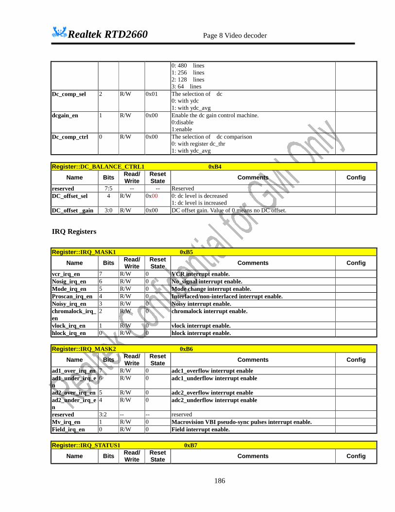
Realtek RTD2660 Page 8 Video decoder
186
0: 480 lines 1: 256 lines 2: 128 lines 3: 64 lines
Dc_comp_sel 2 R/W 0x01 The selection of dc 0: with ydc 1: with ydc_avg
dcgain_en 1 R/W 0x00 Enable the dc gain control machine. 0:disable 1:enable
Dc_comp_ctrl 0 R/W 0x00 The selection of dc comparison 0: with register dc_thr 1: with ydc_avg
Register::DC_BALANCE_CTRL1 0xB4
Name Bits Read/ Write
Reset State Comments Config
reserved 7:5 -- -- Reserved DC_offset_sel 4 R/W 0x00 0: dc level is decreased
1: dc level is increased
DC_offset _gain 3:0 R/W 0x00 DC offset gain. Value of 0 means no DC offset.
IRQ Registers
Register::IRQ_MASK1 0xB5
Name Bits Read/ Write
Reset State Comments Config
vcr_irq_en 7 R/W 0 VCR interrupt enable. Nosig_irq_en 6 R/W 0 No_signal interrupt enable. Mode_irq_en 5 R/W 0 Mode change interrupt enable. Proscan_irq_en 4 R/W 0 Interlaced/non-interlaced interrupt enable. Noisy_irq_en 3 R/W 0 Noisy interrupt enable. chromalock_irq_en
2 R/W 0 chromalock interrupt enable.
vlock_irq_en 1 R/W 0 vlock interrupt enable. hlock_irq_en 0 R/W 0 hlock interrupt enable. Register::IRQ_MASK2 0xB6
Name Bits Read/ Write
Reset State Comments Config
ad1_over_irq_en 7 R/W 0 adc1_overflow interrupt enable ad1_under_irq_en
6 R/W 0 adc1_underflow interrupt enable
ad2_over_irq_en 5 R/W 0 adc2_overflow interrupt enable ad2_under_irq_en
4 R/W 0 adc2_underflow interrupt enable
reserved 3:2 -- -- reserved Mv_irq_en 1 R/W 0 Macrovision VBI pseudo-sync pulses interrupt enable. Field_irq_en 0 R/W 0 Field interrupt enable. Register::IRQ_STATUS1 0xB7
Name Bits Read/ Write
Reset State Comments Config

Realtek RTD2660 Page 8 Video decoder
187
vcr_irq 7 R 0 vcr or vcr_trick flag status change, the IRQ will be triggered. Once IRQ triggered, it must write 1 to clear. Only active when vcr_irq_en = 1.
Nosig_irq 6 R 0 No_signal flag status change, the IRQ will be triggered. Once IRQ triggered, it must write 1 to clear. Only active when nosig_irq_en = 1.
Mode_irq 5 R 0 Reg_decision_mode_status change, the IRQ will be triggered. Once IRQ triggered, it must write 1 to clear. Only active when mode_irq_en = 1.
Proscan_irq 4 R 0 proscan flag status change, the IRQ will be triggered. Once IRQ triggered, it must write 1 to clear. Only active when proscan_irq_en = 1.
Noisy_irq 3 R 0 noisy flag status change, the IRQ will be triggered. Once IRQ triggered, it must write 1 to clear. Only active when noisy_irq_en = 1.
chromalock_irq 2 R 0 Chromalock flag status change, the IRQ will be triggered. Once IRQ triggered, it must write 1 to clear. Only active when lock_irq_en = 1.
vlock_irq 1 R 0 vlock flag status change, the IRQ will be triggered. Once IRQ triggered, it must write 1 to clear. Only active when lock_irq_en = 1.
hlock_irq 0 R 0 hlock flag status change, the IRQ will be triggered. Once IRQ triggered, it must write 1 to clear. Only active when lock_irq_en = 1.
Register::IRQ_STATUS1_WCLR 0xB8
Name Bits Read/ Write
Reset State Comments Config
vcr_irq_wclr_out 7 R/W 0 Wirte 1 to clear Nosig_irq_wclr_out
6 R/W 0 Wirte 1 to clear
Mode_irq_wclr_out
5 R/W 0 Wirte 1 to clear
Proscan_irq_wclr_out
4 R/W 0 Wirte 1 to clear
Noisy_irq_wclr_out
3 R/W 0 Wirte 1 to clear
chromalock_irq_wclr_out
2 R/W 0 Wirte 1 to clear
vlock_irq_wclr_out
1 R/W 0 Wirte 1 to clear
hlock_irq_wclr_out
0 R/W 0 Wirte 1 to clear
Register::IRQ_STATUS2 0xB9
Name Bits Read/ Write
Reset State Comments Config
ad1_overflow_irq
7 R 0 adc1_overflow flag status set, the IRQ will be triggered. Once IRQ triggered, it must write 1 to clear. Only active when ad1_over_irq_en = 1.
ad1_underflow_irq
6 R 0 adc1_underflow flag status set, the IRQ will be triggered. Once IRQ triggered, it must write 1 to clear. Only active when adc1_under_irq_en = 1.
ad2_overflow_irq
5 R 0 adc2_overflow flag status set, the IRQ will be triggered. Once IRQ triggered, it must write 1 to clear. Only active when adc2_over_irq_en = 1.
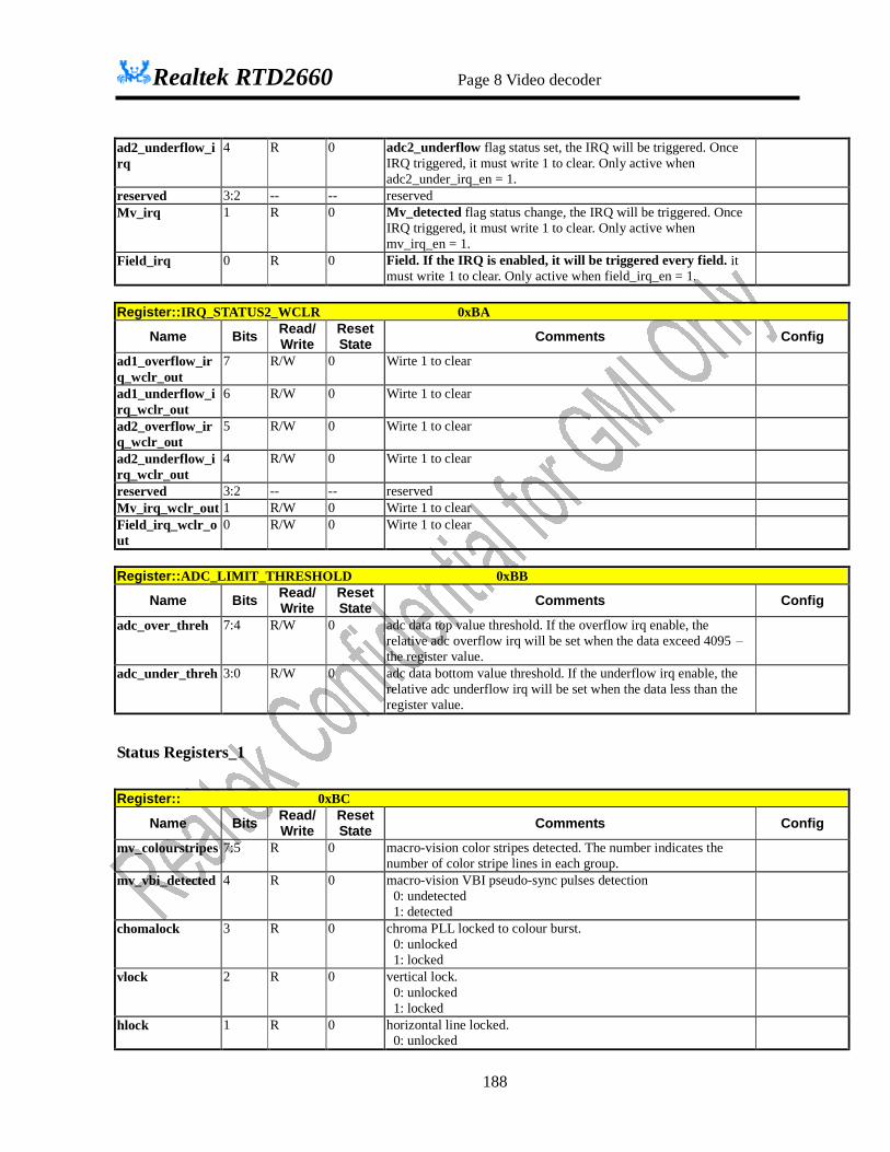
Realtek RTD2660 Page 8 Video decoder
188
ad2_underflow_irq
4 R 0 adc2_underflow flag status set, the IRQ will be triggered. Once IRQ triggered, it must write 1 to clear. Only active when adc2_under_irq_en = 1.
reserved 3:2 -- -- reserved Mv_irq 1 R 0 Mv_detected flag status change, the IRQ will be triggered. Once
IRQ triggered, it must write 1 to clear. Only active when mv_irq_en = 1.
Field_irq 0 R 0 Field. If the IRQ is enabled, it will be triggered every field. it must write 1 to clear. Only active when field_irq_en = 1.
Register::IRQ_STATUS2_WCLR 0xBA
Name Bits Read/ Write
Reset State Comments Config
ad1_overflow_irq_wclr_out
7 R/W 0 Wirte 1 to clear
ad1_underflow_irq_wclr_out
6 R/W 0 Wirte 1 to clear
ad2_overflow_irq_wclr_out
5 R/W 0 Wirte 1 to clear
ad2_underflow_irq_wclr_out
4 R/W 0 Wirte 1 to clear
reserved 3:2 -- -- reserved Mv_irq_wclr_out 1 R/W 0 Wirte 1 to clear Field_irq_wclr_out
0 R/W 0 Wirte 1 to clear
Register::ADC_LIMIT_THRESHOLD 0xBB
Name Bits Read/ Write
Reset State Comments Config
adc_over_threh 7:4 R/W 0 adc data top value threshold. If the overflow irq enable, the relative adc overflow irq will be set when the data exceed 4095 – the register value.
adc_under_threh 3:0 R/W 0 adc data bottom value threshold. If the underflow irq enable, the relative adc underflow irq will be set when the data less than the register value.
Status Registers_1
Register:: 0xBC
Name Bits Read/ Write
Reset State Comments Config
mv_colourstripes 7:5 R 0 macro-vision color stripes detected. The number indicates the number of color stripe lines in each group.
mv_vbi_detected 4 R 0 macro-vision VBI pseudo-sync pulses detection 0: undetected 1: detected
chomalock 3 R 0 chroma PLL locked to colour burst. 0: unlocked 1: locked
vlock 2 R 0 vertical lock. 0: unlocked 1: locked
hlock 1 R 0 horizontal line locked. 0: unlocked

Realtek RTD2660 Page 8 Video decoder
189
1: locked no_signal 0 R 0 no signal detection.
0: signal detected 1: no signal detected
Register::VIDEO_STATUS_REG2 0xBD
Name Bits Read/ Write
Reset State Comments Config
reserved 7:5 -- -- Reserved. Detect443_flag 4 R 0 Freq 4.43MHz flag
Burst frequency is near 4.43MHz or near 3.58MHz.
Burst_detect 3 R 0 If burst magnitude is big enough. 0 : no burst detected 1 : burst detected
PALor_flag 2 R 0 PALm flag or pal flag PALm_flag 1 R 0 PAL color mode detected. proscan_detected 0 R 0 progressive scan detected. Register::VIDEO_STATUS_REG3 0xBE
Name Bits Read/ Write
Reset State Comments Config
vcr_rew 7 R 0 VCR rewind detected. vcr_ff 6 R 0 VCR fast-forward detected. vcr_trick 5 R 0 VCR trick-mode detected. vcr 4 R 0 VCR detected. noisy 3 R 0 noisy signal detected. This bit is set when the detected noise value
(status register 7Fh) is greater than the value programmed into the “noise_thresh” register (05h).
Lines_625_detected
2 R 0 625 scan lines detected.
SECAM_detected
1 R 0 SECAM color mode detected.
PAL_detected 0 R 0 PAL color mode detected. Register::NOISE_THRESHOLD 0xBF
Name Bits Read/ Write
Reset State Comments Config
noise_thresh 7:0 R/W 0x32 sets the noise value at which the circuit considers a signal noisy. The detected noise value may be read back through register 7Fh (“status_noise”). If the detected noise value is greater than “noise_thresh”, then register bit 3C.3h (“noisy”) is set. Larger values of “status_noise” indicate noisier signals, so larger values of “noise_thresh” decreases the likelihood of “noisy” being set while smaller values of “noise_thresh” increases the likelihood of “noisy” being set.
Status Registers_2
Register::HDTO_INC_STATUS4 0xC0
Name Bits Read/ Write
Reset State Comments Config
reserved 7:6 -- -- reserved. hdto_inc[29:24] 5:0 R 0 status bits 29:24 of the 30-bit-wide horizontal sync DTO

Realtek RTD2660 Page 8 Video decoder
190
increment. Register::HDTO_INC_STATUS3 0xC1
Name Bits Read/ Write
Reset State Comments Config
hdto_inc[23:16] 7:0 R 0 status bits 23:16 of the 30-bit-wide horizontal sync DTO increment.
Register::HDTO_INC_STATUS2 0xC2
Name Bits Read/ Write
Reset State Comments Config
hdto_inc[15:8] 7:0 R 0 status bits 15:8 of the 30-bit-wide horizontal sync DTO increment. Register::HDTO_INC_STATUS1 0xC3
Name Bits Read/ Write
Reset State Comments Config
hdto_inc[7:0] 7:0 R 0 status bits 7:0 of the 30-bit-wide horizontal sync DTO increment. Register::CDTO_INC_STATUS4 0xC4
Name Bits Read/ Write
Reset State Comments Config
reserved 7:6 -- -- Reserved. cdto_inc[29:24] 5:0 R 0 status bits 29:24 of the 30-bit-wide chroma sync DTO increment. Register::CDTO_INC_STATUS3 0xC5
Name Bits Read/ Write
Reset State Comments Config
cdto_inc[23:16] 7:0 R 0 status bits 23:16 of the 30-bit-wide chroma sync DTO increment. Register::CDTO_INC_STATUS2 0xC6
Name Bits Read/ Write
Reset State Comments Config
cdto_inc[15:8] 7:0 R 0 status bits 15:8 of the 30-bit-wide chroma sync DTO increment. Register::CDTO_INC_STATUS1 0xC7
Name Bits Read/ Write
Reset State Comments Config
cdto_inc[7:0] 7:0 R 0 status bits 7:0 of the 30-bit-wide chroma sync DTO increment. Register::AGC_DGAIN_STATUS2 0xC8
Name Bits Read/ Write
Reset State Comments Config
agc_dgain[11:8] 7:0 R 0 digital AGC gain value[11:8]. Register::AGC_DGAIN_STATUS1 0xC9
Name Bits Read/ Write
Reset State Comments Config
agc_dgain[7:0] 7:0 R 0 digital AGC gain value[7:0]. Register::CMAG_STATUS 0xCA
Name Bits Read/ Write
Reset State Comments Config
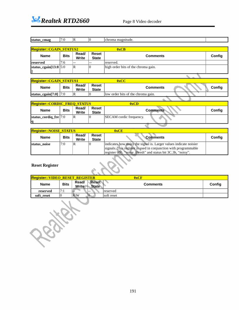
Realtek RTD2660 Page 8 Video decoder
191
status_cmag 7:0 R 0 chroma magnitude. Register::CGAIN_STATUS2 0xCB
Name Bits Read/ Write
Reset State Comments Config
reserved 7:6 -- -- reserved. status_cgain[13:8]
5:0 R 0 high order bits of the chroma gain.
Register::CGAIN_STATUS1 0xCC
Name Bits Read/ Write
Reset State Comments Config
status_cgain[7:0] 7:0 R 0 low order bits of the chroma gain. Register::CORDIC_FREQ_STATUS 0xCD
Name Bits Read/ Write
Reset State Comments Config
status_cordiq_freq
7:0 R 0 SECAM cordic frequency.
Register::NOISE_STATUS 0xCE
Name Bits Read/ Write
Reset State Comments Config
status_noise 7:0 R 0 indicates how noisy the signal is. Larger values indicate noisier signals. This register is used in conjunction with programmable register 05h, “noise_thresh” and status bit 3C.3h, “noisy”.
Reset Register
Register::VIDEO_RESET_REGISTER 0xCF
Name Bits Read/ Write
Reset State Comments Config
reserved 7:1 -- -- reserved soft_reset 0 R/W 0 soft reset

Realtek RTD2660 Page 8 Video decoder
192
Auto Mode State Machine Registers.
Register::palm_flag_compensation1 0xD0
Name Bits Read/ Write
Reset State Comments Config
reserved 7:6 - -- Reserved. palm_atone_counter
5:0 R/W 0x10 palm flag compensation counter.
Register::palm_flag_compensation2 0xD1
Name Bits Read/ Write
Reset State Comments Config
palm_atone_threshold
7:0 R/W 0 palm flag compensation threshold. The value of register must be added by 200. 0 + 200*1 = 200
Register::manual_mode 0xD2
Name Bits Read/ Write
Reset State Comments Config
auto_mode_en 7 R/W 1 Auto mode detection enable register. When bit6 is 0, reference to this bit. 1: enable. Use auto mode. 0: disable. Use manual mode.
auto_625only_en 6 R/W 0 Auto 625-only enable bit. 1: enable auto 625 detection only, no matter bit7 is 0 or 1. 0: reference to bit7.
Auto_burst_switch_625only
5 R/W 0 Auto 625 only mode switch, when burst detection is 0 0 : disable 1 : enable
reserved 4 -- -- reserved state_machine_re
set 3 R/W 0 Reset auto mode state machine.
1 : reset 0 : normal
manual_mode_select
2:0 R/W 0 Select a mode when bit3 is 0. 0: ntsc. 1: palm. 2: ntsc50. 3: paln. 4: ntsc443. 5: pal60. 6: pali. 7: secam.
Register::mode_detection_status 0xD3
Name Bits Read/ Write
Reset State Comments Config
reserved 7 - - reserved set_mode_status 6:4 R 0 Setting mode status.
0: ntsc. 1: palm.

Realtek RTD2660 Page 8 Video decoder
193
2: ntsc50. 3: paln. 4: ntsc443. 5: pal60. 6: pali. 7: secam.
reserved 3 - - reserved decision_mode_st
atus 2:0 R 0 Auto mode detection result.
0: ntsc. 1: palm. 2: ntsc50. 3: paln. 4: ntsc443. 5: pal60. 6: pali. 7: secam.
Register::statistic_and_disable_mode 0xD4
Name Bits Read/ Write
Reset State Comments Config
disable_mode_en 7 R/W 0 Disable mode enable register. 1: enable. 0 : disable.
disable_mode 6 R/W 0 Disable 625 or 525 mode when bit7 is 1. 1: disable 625 input. 0: disable 525 input.
statistic_number 5:0 R/W 4 Number of frame to delay and calculate statistic﹐when vcr or noisy happens. Default 4 means 4 frames.
Register::prefer_mode 0xD5
Name Bits Read/ Write
Reset State Comments Config
prefer_ntsc50_paln
7 R/W 0 Prefer ntsc50 or paln when bit3 is 1. 1: ntsc50. 0: paln.
prefer_ntsc443_pal60
6 R/W 0 Prefer ntsc443 or pal60 when bit2 is 1. 1: ntsc443. 0: pal60.
prefer_secam_pali
5 R/W 0 Prefer secam or pali when bit1 is 1. 1: secam. 0: pali.
prefer_ntsc_palm 4 R/W 0 Prefer ntsc or palm when bit0 is 1. 1: ntsc. 0: palm.
prefer_ntsc50_paln_en
3 R/W 0 Prefer ntsc50 or paln enable register. 1: enable. 0: disable.
prefer_ntsc443_pal60_en
2 R/W 0 Prefer ntsc443 or pal60 enable register. 1: enable. 0: disable.
prefer_secam_pali_en
1 R/W 0 Prefer secam or pali enable register. 1: enable. 0: disable.
prefer_ntsc_palm 0 R/W 0 Prefer ntsc or palm enable register.

Realtek RTD2660 Page 8 Video decoder
194
_en 1: enable. 0: disable.
Register::state_machine_fix_mode 0xD6
Name Bits Read/ Write
Reset State Comments Config
Fix_625flag_en 7 R/W 0 In auto mode state machine﹐enable fix 625 flag mode 0 : disable﹐use real 625 flag 1 : enable﹐reference to bit3
Fix_443flag_en 6 R/W 0 In auto mode state machine﹐enable fix 443 flag mode 0 : disable﹐use real 443 flag 1 : enable﹐reference to bit2
Fix_palorflag_en 5 R/W 0 In auto mode state machine﹐enable fix palor flag mode 0 : disable﹐use real palor flag 1 : enable﹐reference to bit1
Fix_secamflag_en 4 R/W 0 In auto mode state machine﹐enable fix secam flag mode 0 : disable﹐use real secam flag 1 : enable﹐reference to bit0
Fix_625_h 3 R/W 0 If bit7 is 1﹐fix 625 flag in auto mode state machine 0 : low 1 : high
Fix_443_h 2 R/W 0 If bit6 is 1﹐fix 443 flag in auto mode state machine 0 : low 1 : high
Fix_palor_h 1 R/W 0 If bit5 is 1﹐fix palor flag in auto mode state machine 0 : low 1 : high
Fix_secam_h 0 R/W 0 If bit4 is 1﹐fix secam flag in auto mode state machine 0 : low 1 : high
Register::zoran_register_enable 0xD7
Name Bits Read/ Write
Reset State Comments Config
Hactivestartreg_en
7 R/W 0 Enable register from zoran. Include reg_hactive_start.. 1: enable. 0: disable.
Hpixelreg_en 6 R/W 0 Enable register from zoran. Include reg_hpixel. 1: enable. 0: disable.
Colourmodereg_en
5 R/W 0 Enable register from zoran. Include reg_colour_mode. 1: enable. 0: disable.
Hagcreg_en 4 R/W 0 Enable register from zoran. Include reg_hagc. 1: enable. 0: disable.
vline625reg_en 3 R/W 0 Enable register from zoran. Include reg_vline_625. 1: enable. 0: disable.
Cdtomem_reg_en 2 R/W 0 Enable register from zoran. Include reg_cdto_inc. 1: enable. 0: disable.

Realtek RTD2660 Page 8 Video decoder
195
Vsyncreg_en 1 R/W 0 Enable register from zoran. Include reg_vactive_start, reg_vactive_height. 1: enable. 0: disable.
Ped_reg_en 0 R/W 0 Enable register from zoran. Include reg_ped and reg_cagc_en. 1: enable. 0: disable.
Register::auto_mode_state_machine_statistic 0xD8
Name Bits Read/ Write
Reset State Comments Config
switch_palo_palm_method
7:6 R/W 0 Choose pal flag for state machine, 3 methods 0 : palor flag 1 : palo flag 2 : palm flag 3 : reserved
auto_secam_pali_method
5:4 R/W 0 Choose secam pali decision method. 4 methods 0 : secam flag 1 : pal flag 2 : pal flag is high and secam flag is low 3 : secam flag is high and pal flag is low
Secam_flag_freq_disable
3 R/W 1 Secam flag freq condition disable. 0 : enable 1 : disable
Statistic_multiplier
2:0 R/W 3 Auto mode state machine﹐statistic multiplier number.
Address: 0xD9 Reserved
Comb Filter Configuration Register
Register::COMB_FILTER_CONFIG 0xDA
Name Bits Read/ Write
Reset State Comments Config
reserved 7 -- -- reserved PAL_perr 6 R/W 1 used to reduce phase-error artifacts in the comb filter’s luma-path.
It should be set for VCR signals. 0: off 1: on
PAL_perr_auto_en
5 R/W 0 turn on the PAL_perr when VCR signals is detected.
reserved 4:2 -- -- reserved PALsw_level 1:0 R/W 2 determine how many incorrect lines are used for the PAL switch
circuit before switching. Use a higher level for noisy signals.
Comb Filter Threshold Registers
Register::COMB_FILTER_THRESHOLD1 0xDB

Realtek RTD2660 Page 8 Video decoder
196
Name Bits Read/ Write
Reset State Comments Config
noise_ntsc_c 7:0 R/W 0x07 used to tune the noise_threshold used by the comb filter for NTSC. Register::COMB_FILTER_THRESHOLD2 0xDC
Name Bits Read/ Write
Reset State Comments Config
noise_pal_c 7:0 R/W 0x20 used to tune the noise_threshold used by the comb filter for PAL. Register::COMB_FILTER_THRESHOLD3 0xDD
Name Bits Read/ Write
Reset State Comments Config
noise_phase_c 7:0 R/W 0x03 used to tune the noise_threshold used by the chroma comb filter. Register::COMB_FILTER_THRESHOLD4 0xDE
Name Bits Read/ Write
Reset State Comments Config
noise_phase_y 7:0 R/W 0x10 used to tune the noise_threshold used by the luma comb filter Address: 0xDF Reserved
2D YC Separation Registers
Register::YC_SEP_CONTROL 0xE0
Name Bits Read/ Write
Reset State Comments Config
reserved 7:3 -- -- adaptive_mode 2:0 R/W 0 adaptive_mode: select modes for the composite signal’s luma (Y)
and chroma (C) separation before color demodulation.
000: fully adaptive comb (2-D adaptive comb) :Y 1/2/3 C 1/2/3
010: --
010: 5-tap adaptive comb filter (PAL mode only) :Y 1/3/5 C
1/3/5
011: basic luma notch filter mode (for very noisy and unstable
pictures)
(不經過 line buffer 的結果)
100: Y 2/3/4 C 1/3/5 101: ---
110: 5-tap hybrid adaptive comb filter (PAL mode only) : Y 1/3/5 C 2/3/4
Register::BPF_BW_SEL_Y 0xE1
Name Bits Read/ Write
Reset State Comments Config
reserved 7 -- -- reserved wide_bpf _sel_y 6:4 R/W 4 000: 0.65Mhz (Coefficient: [-8, 0, 17, 0, -25, 0, 28, 0, -25, 0, 17,

Realtek RTD2660 Page 8 Video decoder
197
0,-8])
001: 0.8Mhz (Coefficient: [-2, 0, 13, 0, -30, 0, 38, 0, -30, 0, 13,
0, -2])
010: 1.0Mhz (Coefficient: [3, 0, 6, 0, -35, 0, 52, 0, -35, 0, 6, 0, 3])
011: 1.3Mhz (Coefficient: [3, 0, 3, 0, -35, 0, 58, 0, -35, 0, 3, 0, 3])
100: 1.5Mhz (Coefficient: [4, 0, 1, 0, -36, 0, 62, 0, -36, 0, 1, 0, 4])
101: 1.8Mhz (Coefficient: [6, 0, -3, 0, -38, 0, 70, 0, -38, 0, -3, 0, 6]) 110: 2.1Mhz (Coefficient: [-2, 0, -13, 0, -31, 0, 88, 0, -31, 0, -13, 0, -2]) 111: 2.6MHz(Coefficient: [-12, 0, -17, 0, -20, 0, 98, 0, -20, 0, -17, 0, -12])
reserved 3 -- -- reserved narrow_bpf
_sel_y 2:0 R/W 3 000: 0.65Mhz (Coefficient: [-8, 0, 17, 0, -25, 0, 28, 0, -25, 0, 17,
0,-8])
001: 0.8Mhz (Coefficient: [-2, 0, 13, 0, -30, 0, 38, 0, -30, 0, 13,
0, -2])
010: 1.0Mhz (Coefficient: [3, 0, 6, 0, -35, 0, 52, 0, -35, 0, 6, 0, 3])
011: 1.3Mhz (Coefficient: [3, 0, 3, 0, -35, 0, 58, 0, -35, 0, 3, 0, 3])
100: 1.5Mhz (Coefficient: [4, 0, 1, 0, -36, 0, 62, 0, -36, 0, 1, 0, 4])
101: 1.8Mhz (Coefficient: [6, 0, -3, 0, -38, 0, 70, 0, -38, 0, -3, 0, 6]) 110: 2.1Mhz (Coefficient: [-2, 0, -13, 0, -31, 0, 88, 0, -31, 0, -13, 0, -2]) 111: 2.6MHz(Coefficient: [-12, 0, -17, 0, -20, 0, 98, 0, -20, 0, -17, 0, -12])
Register::BPF_BW_SEL_C 0xE2
Name Bits Read/ Write
Reset State Comments Config
reserved 7 -- -- reserved wide_bpf _sel_c 6:4 R/W 6 000: 0.65Mhz (Coefficient: [-8, 0, 17, 0, -25, 0, 28, 0, -25, 0, 17,
0,-8])
001: 0.8Mhz (Coefficient: [-2, 0, 13, 0, -30, 0, 38, 0, -30, 0, 13,
0, -2])
010: 1.0Mhz (Coefficient: [3, 0, 6, 0, -35, 0, 52, 0, -35, 0, 6, 0, 3])
011: 1.3Mhz (Coefficient: [3, 0, 3, 0, -35, 0, 58, 0, -35, 0, 3, 0, 3])
100: 1.5Mhz (Coefficient: [4, 0, 1, 0, -36, 0, 62, 0, -36, 0, 1, 0, 4])
101: 1.8Mhz (Coefficient: [6, 0, -3, 0, -38, 0, 70, 0, -38, 0, -3, 0, 6]) 110: 2.1Mhz (Coefficient: [-2, 0, -13, 0, -31, 0, 88, 0, -31, 0, -13, 0, -2]) 111: 2.6MHz(Coefficient: [-12, 0, -17, 0, -20, 0, 98, 0, -20, 0, -17, 0, -12])
reserved 3 -- -- reserved
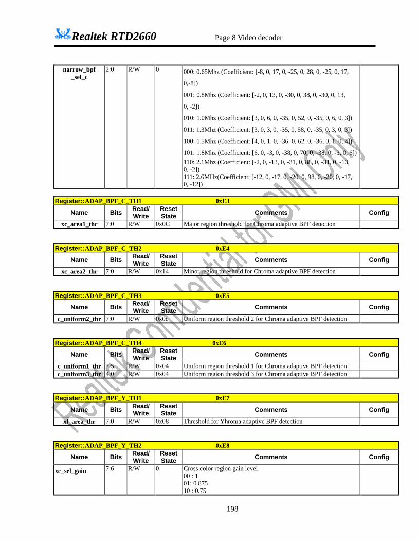
Realtek RTD2660 Page 8 Video decoder
198
narrow_bpf _sel_c
2:0 R/W 0 000: 0.65Mhz (Coefficient: [-8, 0, 17, 0, -25, 0, 28, 0, -25, 0, 17,
0,-8])
001: 0.8Mhz (Coefficient: [-2, 0, 13, 0, -30, 0, 38, 0, -30, 0, 13,
0, -2])
010: 1.0Mhz (Coefficient: [3, 0, 6, 0, -35, 0, 52, 0, -35, 0, 6, 0, 3])
011: 1.3Mhz (Coefficient: [3, 0, 3, 0, -35, 0, 58, 0, -35, 0, 3, 0, 3])
100: 1.5Mhz (Coefficient: [4, 0, 1, 0, -36, 0, 62, 0, -36, 0, 1, 0, 4])
101: 1.8Mhz (Coefficient: [6, 0, -3, 0, -38, 0, 70, 0, -38, 0, -3, 0, 6]) 110: 2.1Mhz (Coefficient: [-2, 0, -13, 0, -31, 0, 88, 0, -31, 0, -13, 0, -2]) 111: 2.6MHz(Coefficient: [-12, 0, -17, 0, -20, 0, 98, 0, -20, 0, -17, 0, -12])
Register::ADAP_BPF_C_TH1 0xE3
Name Bits Read/ Write
Reset State Comments Config
xc_area1_thr 7:0 R/W 0x0C Major region threshold for Chroma adaptive BPF detection Register::ADAP_BPF_C_TH2 0xE4
Name Bits Read/ Write
Reset State Comments Config
xc_area2_thr 7:0 R/W 0x14 Minor region threshold for Chroma adaptive BPF detection Register::ADAP_BPF_C_TH3 0xE5
Name Bits Read/ Write
Reset State Comments Config
c_uniform2_thr 7:0 R/W 0x0c Uniform region threshold 2 for Chroma adaptive BPF detection Register::ADAP_BPF_C_TH4 0xE6
Name Bits Read/ Write
Reset State Comments Config
c_uniform1_thr 7:5 R/W 0x04 Uniform region threshold 1 for Chroma adaptive BPF detection c_uniform3_thr 4:0 R/W 0x04 Uniform region threshold 3 for Chroma adaptive BPF detection
Register::ADAP_BPF_Y_TH1 0xE7
Name Bits Read/ Write
Reset State Comments Config
xl_area_thr 7:0 R/W 0x08 Threshold for Yhroma adaptive BPF detection Register::ADAP_BPF_Y_TH2 0xE8
Name Bits Read/ Write
Reset State Comments Config
xc_sel_gain 7:6 R/W 0 Cross color region gain level 00 : 1 01: 0.875 10 : 0.75

Realtek RTD2660 Page 8 Video decoder
199
11 : 0.625 pal_malpha_lut 5:4 R/W 0x01 Blending table for pal
00: original table 01: new table 10 : reserved 11: reserved
y_uniform_thr 3:0 R/W 3 Uniform region threshold for Yhroma adaptive BPF detection
Register::ADAP_BPF_Y_TH3 0xE9
Name Bits Read/ Write
Reset State Comments Config
Malpha_c_divide
r2_sel
7 R/W 0
malpha_y_divide
r2_sel
6 R/W 0
malpha_y_en 5 R/W 0 Malpha for Y
malpha_y 4 R/W 0 malpha_y value when malpha_y_en=1 1 : Malpha_y =16 0 : Malpha_y = 0
malpha_c_en 3 R/W 0 Malpha for C
malpha_c 2 R/W 0 malpha_y value when malpha_c_en=1 1 : Malpha_c =16 0 : Malpha_c = 0
yalpha_en 1 R/W 0 yalpha enable
yalpha 0 R/W 0 yalpha value when yalpha _en=1 1 : yalpha =16 0 : yalpha = 0
Register::YC_BW_CTRL 0xEA
Name Bits Read/ Write
Reset State Comments Config
reserved 7 -- -- reserved pal_demod_sel 6 R/W 0 select the demodulation filter before chroma low pass filter.
0: [1 1]/2 1: [1 2 1]/4
reserved 5:4 -- -- reserved chroma_vlpf_en 3 R/W 0 chroma vertical low pass filter enable.
0: disabled 1: vertical low pass filter
chroma_bw_lo 2:0 R/W 1 set the chroma low pass filter to wide or narrow. for NTSC: (with 0 between each coefficients) 000 Bypass mode 001 3.6Mhz [0 0 0 0 0 1 1 0 0 0 0 0] 010 2.9Mhz [0 1 -7 -11 36 109 109 36 -11 -7 1 0] 011 2.4Mhz [0 0 -18 4 51 91 91 51 4 -18 0 0] 100 2.1Mhz [0 -3 -6 6 45 86 86 45 6 -6 -3 0] 101 1.8Mhz [-5 -7 0 21 49 70 70 49 21 0 -7

Realtek RTD2660 Page 8 Video decoder
200
-5] 110 1.2Mhz [-2 2 11 25 41 51 51 41 25 11 2 -2] 111 0.8Mhz [3 8 16 26 35 40 40 35 26 16 8 3]
Register::2D_DEBUG_MODE 0xEB
Name Bits Read/ Write
Reset State Comments Config
reserved 7 -- -- reserved mden_plus_sel 6:5 R/W 00 00: 2610 case
01: enable LPF decision 10: disable Mden_plus 11: enable Mden_plus
debug_mode_2d_en
4 R/W 0 2D debug mode enable
debug_mode_2d 3:0 R/W 0 0000 : narrow BPF region for Cchroma 0001 : XC region 0010 : uniform region for Cchroma 0011 : wide BPF region for Ychroma 0100 : XL region 0101 : uniform region for Ychroma 0110 : Malpha_y 0111 : Malpha_c 1000 : Yalpha 1001 : Calpha 1010 : no_hor_tmp=1 1011 : hortendency=1 1100 :1d blend 1101 : BW 1110 : h2v
Register::RESOL_LP_THR 0xEC
Name Bits Read/ Write
Reset State Comments Config
reso_lp_thr 7:0 R/W 0x14
Register::Envelope_THR 0xED
Name Bits Read/ Write
Reset State Comments Config
reserved 7 -- -- horcrossluma_en 6 R/W 0 Enable horizontal decision when horcrossluma_en=1
envelpe_thr 5:0 R/W 4
Register::Comb_filter_THR5 0xEE
Name Bits Read/ Write
Reset State Comments Config
horcrossluma_m
ode
7:5 R/W 0 horizontal decision mode when horcrossluma_en=1 000 : mden<4 001 : mnom_vdy>mden*2
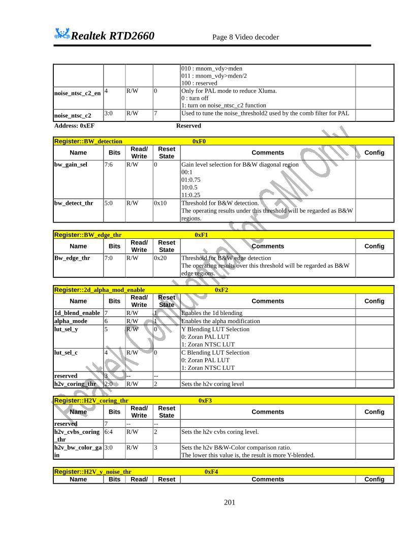
Realtek RTD2660 Page 8 Video decoder
201
010 : mnom_vdy>mden 011 : mnom_vdy>mden/2 100 : reserved
noise_ntsc_c2_en 4 R/W 0 Only for PAL mode to reduce Xluma. 0 : turn off 1: turn on noise_ntsc_c2 function
noise_ntsc_c2 3:0 R/W 7 Used to tune the noise_threshold2 used by the comb filter for PAL
Address: 0xEF Reserved Register::BW_detection 0xF0
Name Bits Read/ Write
Reset State Comments Config
bw_gain_sel 7:6 R/W 0 Gain level selection for B&W diagonal region 00:1 01:0.75 10:0.5 11:0.25
bw_detect_thr 5:0 R/W 0x10 Threshold for B&W detection. The operating results under this threshold will be regarded as B&W regions.
Register::BW_edge_thr 0xF1
Name Bits Read/ Write
Reset State Comments Config
Bw_edge_thr 7:0 R/W 0x20 Threshold for B&W edge detection The operating results over this threshold will be regarded as B&W edge regions.
Register::2d_alpha_mod_enable 0xF2
Name Bits Read/ Write
Reset State Comments Config
1d_blend_enable 7 R/W 1 Enables the 1d blending alpha_mode 6 R/W 1 Enables the alpha modification lut_sel_y 5 R/W 0 Y Blending LUT Selection
0: Zoran PAL LUT 1: Zoran NTSC LUT
lut_sel_c 4 R/W 0 C Blending LUT Selection 0: Zoran PAL LUT 1: Zoran NTSC LUT
reserved 3 -- -- h2v_coring_thr 2:0 R/W 2 Sets the h2v coring level Register::H2V_coring_thr 0xF3
Name Bits Read/ Write
Reset State Comments Config
reserved 7 -- -- h2v_cvbs_coring_thr
6:4 R/W 2 Sets the h2v cvbs coring level.
h2v_bw_color_gain
3:0 R/W 3 Sets the h2v B&W-Color comparison ratio. The lower this value is, the result is more Y-blended.
Register::H2V_y_noise_thr 0xF4
Name Bits Read/ Reset Comments Config

Realtek RTD2660 Page 8 Video decoder
202
Write State h2v_y_noise_thr 7:0 R/W 8 Noise threshold for h2v Y signal. Register::H2V_cvbs_noise_thr 0xF5
Name Bits Read/ Write
Reset State Comments Config
h2v_cvbs_noise_thr
7:0 R/W 8 Noise threshold for h2v cvbs signal.
Register::H2V_blend_ratio 0xF6
Name Bits Read/ Write
Reset State Comments Config
reserved 7:3 -- -- h2v_blendratio 2:0 R/W 4 Adjusts the positive shift number of h2v blending factors.
The higher this value is, the more 2D-approached LUT is resulted.
Register::1D_blend_thr 0xF7
Name Bits Read/ Write
Reset State Comments Config
reserved 7 -- -- 1d_blend_thr 6:2 R/W 2 Threshold for 1d blending
The operating results over this threshold will be applied with 1d blending.
1d_bpf_sel_y 1:0 R/W 0 Y BPF selection for 1d blending Register::1D_blend_bpf_sel 0xF8
Name Bits Read/ Write
Reset State Comments Config
reserved 7 -- -- 1d_narrow_bpf_sel_c
6:4 R/W 0 C Narrow BPF selection for 1d blending
reserved 3 -- -- 1d_wide_bpf_sel_c
2:0 R/W 2 C Wide BPF selection for 1d blending
Address: 0xF9~0xFF Reserved

Realtek RTD2660 Page 9 Video Decoder
203
Page 9 Video Decoder
Clamping/AGC Control Registers
Register::AGC_PEAK_NOMINAL 0xA0
Name Bits Read/ Write
Reset State Comments Config
reserved 7 -- -- reserved agc_peak_nominal
6:0 R/W 0x0a set the luma peak white detection’s AGC nominal peak white value. This value is added to 128 and then the result is multiplied by 4
Register::AGC_PEAK_AND_GATE_CTRL 0xA1
Name Bits Read/ Write
Reset State Comments Config
agc_gate_vsync_coarse
7 R/W 1 forces coarse sync-tip and backproch gates to be used during vsync when VCRs are detected. 0: off 1: on
agc_gate_vsync_stip
6 R/W 0 forces sync-tip clamping during vsync. 0: off 1: on
agc_gate_kill_mode
5:4 R/W 3 method that sync-tip and backporch gates are suppressed 00: off 01: enabled – if sync-tip gate is killed, kill backproch gate 10: enabled – if sync-tip gate is killed, kill backproch gate, except during vsync 11: enabled – if sync-tip gate is killed, don’t kill backporch gate
agc_peak_en 3 R/W 1 enables the AGC peak white detector 0: disable 1: enable
agc_peak_cntl 2:0 R/W 1 set the time constant for the AGC peak white detector Register::AGC_PEAK_CTRL 0xA2
Name Bits Read/ Write
Reset State Comments Config
unlock_peakrst_
en 7 R/W 1 peak gain will reset to 0 when H is unlock
1: enable 0: disable
reserved 6:2 -- -- reserved
agc_peak_loop_g
ain 1:0 R/W 0 peak gain selection
00 : 1/1 (original) 01 : 1/ 8 10 : 1/32 11 : 1/64

Realtek RTD2660 Page 9 Video Decoder
204
Register::VIDEO_CONTROL2 0xA3
Name Bits Read/ Write
Reset State Comments Config
hagc_field_mode 7 R/W 0 when this bit is “0”, then the gain is updated once per line, after DC clamping. When this bit is set, then the gain is only updated once per field, at the start of vertical blank. 0: off 1: on
mv_hagc_mode 6 R/W 1 when set, automatically reduces the gain (set in register 0x04) by 25% when macro-vision encoded signals are detected. 0: off 1: on
Dc_clamp_mode 5:4 R/W 0 sets the mode for analog front end DC clamping. 00: auto; use backporch when a signal exists; use synctip if no signal exists 01: backporch only 10: synctip only 11: off
reserved 3:2 R/W 0 reserved cagc_en 1 R/W 1 enables the chroma AGC. If disabled, then the AGC target is used
to drive directly the AGC gain. 0: off 1: on
hagc_en 0 R/W 1 enables the luma/composite AGC. If disabled, then the AGC target (register 0x04h) is used to drive directly the AGC gain. 0: off 1: on
Register::LUMA_AGC_VALUE 0xA4
Name Bits Read/ Write
Reset State Comments Config
hagc 7:0 R/W 0xdd specifies the luma AGC target value. The gain of the AGC is modified until the horizontal sync height is equal to this value. Note that if a macro-vision signal is detected and “mv_hagc” (02.6h) is set, then this value is automatically reduced by 25%. NTSC M: 0xddh (default) NTSC J: 0xcdh PAL B, D, G, H, COMB N, SECAM: 0xdch PAL M, N: 0xddh NTSC M (MACROVISION): 0xa6h PAL B, D, G, H, I, COMB N (MACROVISION): 0xaeh If “hage_en” (register 02.0h) is “0”, then “hagc” is used to directly drive the analog gain. In this case, a value of 64 represents a unity gain, 32 represents a one-half gain, and 128 denoted a double gain.
Register::AGC_GATE_START_M 0xA5
Name Bits Read/ Reset Comments Config

Realtek RTD2660 Page 9 Video Decoder
205
Write State reserved 7:3 -- -- reserved agc_gate_start[10:8]
2:0 R/W 0x04 delay from the detected hsync for the rough gate generator (MSB [10:8]).
Register::AGC_GATE_START_L 0xA6
Name Bits Read/ Write
Reset State Comments Config
agc_gate_start[7:0]
7:0 R/W 0x00 delay from the detected hsync for the rough gate generator (LSB [7:0]).
Register::AGC_GATE_WIDTH 0xA7
Name Bits Read/ Write
Reset State Comments Config
reserved 7 -- -- reserved agc_gate_width 6:0 R/W 0x40 width of the rough gates Register::AGC_BP_DELAY 0xA8
Name Bits Read/ Write
Reset State Comments Config
agc_bp_delay 7:0 R/W 0x64 set the time delay from the sync tip gate to the backporch gate for the rough gate generator.
Register::CLAMPAGC_COMPLUMA_NEW_THRESHOLD2 0xA9
Name Bits Read/ Write
Reset State Comments Config
reserved 7:6 -- -- Reserved.
clampagc_under_th2
5:0 R/W 0x3F Threshold2 for clampagc_compluma_new.
Register::CLAMPAGC_COMPLUMA_NEW_THRESHOLD1 0xAA
Name Bits Read/ Write
Reset State Comments Config
under_flag 7 R 0 1: under threshold occurs.
0: normal
under_flag_wclr
_out 6 R/W 0 Wirte 1 to clear
reserved 5:4 -- -- Reserved. clampagc_under
_th1 3:0 R/W 0x00 threshold for clampagc_compluma_new.
clampagc_compluma_new under this threshold will decrease
dgain to avoid data underflow.
Register::CLAMPAGC_COMPLUMA_NEW_CONTROL 0xAB
Name Bits Read/ Write
Reset State Comments Config
clampagc_under_cntl
7:2 R/W 0 Set the time constant for the agc bottom gain detector.

Realtek RTD2660 Page 9 Video Decoder
206
clampagc_under_en
1 R/W 1 clampagc_under_th on/off 0: off 1: on
blank_vid_offset 0 R/W 1 Set the interna_blank_vid_level value. 0: 192 1: 240
Register::VSYNC_AGC_MIN 0xAC
Name Bits Read/ Write
Reset State Comments Config
reserved 7 -- -- Reserved. vsync_agc_min 6:0 R/W 0x6C defines the number of half-lines before the vsync that the AGC,
SYNCTIP, and BACKPORCH gates are disabled. (df: -20)
Register::VSYNC_AGC_LOCKOUT_END 0xAD
Name Bits Read/ Write
Reset State Comments Config
vsync_clamp_mode
7:6 R/W 0x02 control DC clamping during the vertical blanking intercal. 00: disabled 01: enabled 10: enabled except for noisy signals 11: enabled only for clean VCR signals
vsync_agc_max 5:0 R/W 0x10 defines the number of half-lines after the vsync that the AGC, SYNCTIP, and BACKPORCH gates are re-enabled.
Address : 0xAE ~0x AF Reserved Register::CHARGE_PUMP_DELAY_CONTROL 0xB0
Name Bits Read/ Write
Reset State Comments Config
cpump_adjust_delay
7:2 R/W 0x0A delay, relative to charge-pump pulses, before adjustment, used to Compensate for possible visible artifacts caused by charge-pump pulses, is applied.
cpump_adjust_polarity
1 R/W 0 polarity of adjustment used to compensate for possible visible Artifacts caused by charge-pump pulses.
cpump_delay_en 0 R/W 0 enable delay of charge-pump up/down pulses. 0: disabled 1: enabled
Register::CHARGE_PUMP_ADJUSTMENT 0xB1
Name Bits Read/ Write
Reset State Comments Config
cpump_adjust 7:0 R/W 0xC8 used to compensate for possible visible artifacts caused by charge-pump pulses.
Register::CHARGE_PUMP_DELAY 0xB2
Name Bits Read/ Write
Reset State Comments Config
cpump_delay 7:0 R/W 0xB9 If “cpump_delay_en=1”, then the charge pump up/down pulses are delayed by “4xcpump_delay” output pixels.
Address : 0xB3 Reserved

Realtek RTD2660 Page 9 Video Decoder
207
Chroma Loop Control Registers
Register::CHROMA_AGC 0xB4
Name Bits Read/ Write
Reset State Comments Config
Cagc 7:0 R/W 0x8A set the chroma AGC target. Register::CHROMA_KILL 0xB5
Name Bits Read/ Write
Reset State Comments Config
user_ckill_mode 7:6 R/W 0 00: auto hardware chroma kill 01: forces chroma kill on 10: forces chroma kill off 11: reserved
VBI_ckill 5 R/W 0 chroma is killed during VBI. 0: off 1: on
hlock_ckill 4 R/W 0 chroma is killed whenever horizontal lock is lost. 0: off 1: on
chroma_kill 3:0 R/W 0x7 set the chroma kill level. Register::CHROMA_LOCK_CONFIG 0xB6
Name Bits Read/ Write
Reset State Comments Config
lose_chromalock_count
7:4 R/W 0x6 used to tune the chromakill, higher values are more sensitive to losing lock.
lose_chromalock_level
3:1 R/W 0x5 set the level for chromakill.
lose_chromalock_ckill
0 R/W 1 when set, chroma is killed whenever chromalock is lost.
Register::CHROMA_LOOPFILTER_GAIN 0xB7
Name Bits Read/ Write
Reset State Comments Config
cnew_gate_en 7 R/W 1 New burst gate enable. For 5 complete sin wave. This gate is only available when fix burst gate is set.
reserved 6:2 -- -- Reserved. cagc_igain 1:0 R/W 0 Cagc loopfilter I-gain value. The cagc responds more slowly when
the smaller gain value is set . 00 : 1 01 : 1/4 10 : 1/16 11 : 1/64
Register::CHROMA_LOOPFILTER_STATE 0xB8
Name Bits Read/ Write
Reset State Comments Config
reserved 7:4 -- -- Reserved. cstate 3:1 R/W 5 sets the chroma loopfilter bandwidth state, larger state has a slower
response.
fixed_cstate 0 R/W 0 when set, fixes the state of chroma loopfilter to cstate.

Realtek RTD2660 Page 9 Video Decoder
208
Register::CHROMA_AUTOPOS 0xB9
Name Bits Read/ Write
Reset State Comments Config
reserved 7 -- -- reserved chroma_burst5or
10 6 R/W 0 selects the burst gate width
0: 5 sub-carrier clock cycles 1: 10 sub-carrier clock cycles
fixed_burstgate 5 R/W 1 this bit disables the burst gate auto-position. The manual burstgate window position is defined by the burst_gate_start (0x2c) and burst_gate_end (0x2d) register. 0: off 1: on 1: on
cautopos 4:0 R/W 0x0c set the chroma burst gate position relative to the auto center position
Address : 0xBA ~ 0xBF Reserved

Realtek RTD2660 Page 9 Video Decoder
209
HPLL Control Registers
Register::LOCK_COUNT 0xC0
Name Bits Read/ Write
Reset State Comments Config
locked_count_noisy_max
7:4 R/W 0x07 set the max value of the hlock sensor for noisy signals. 8 is added to the value.
locked_count_clean_max
3:0 R/W 0x04 set the max value of the hlock seneor for clean signals. 8 is added to the value.
Register::H_LOOP_MAXSTATE 0xC1
Name Bits Read/ Write
Reset State Comments Config
hlock_vsync_mode
7:6 R/W 0x03 control hsync locking during vsync. 00: disabled 01: enabled 10: enable except for noisy signals 11: enable only for clean VCR signals
hstate_fixed 5 R/W 0 forces the state machine to remain in the state set in “hstate_max”. 0: off 1: on
disable_hfine 4 R/W 0 0: off 1: disables the fine mode of the HPLL phase comparator
hstate_unlocked 3 R/W 1 0: off 1: sets the state when unlocked
hstate_max 2:0 R/W 0x03 set the maximum state for the horizontal PLL state machine. The range of this register is 0 to 5, inclusive. Higher states have a finer PLL control. Values of “0” and “1” should not programmed into this register. If “hstate_fixed” is set, then this register is used to force the state.
Register::CLAMPAGC_CTRL0 0xC2
Name Bits Read/ Write
Reset State Comments Config
fine_src_sel 7 R/W 1 the source selection for gate finding when fine mode. 0: low pass filter data 1: original data
coarse_src_sel 6 R/W 0 the source selection for gate finding when coarse mode. 0: low pass filter data 1: original data
fine_gate_sel 5 R/W 1 the gate selection when fine mode. 0: coarse gate 1: fine gate
gate_end_thresh 4:0 R/W 0x0a threshold at which the rough gate generator ends the gate. The real value is multiplied by 64.

Realtek RTD2660 Page 9 Video Decoder
210
Register::CLAMPAGC_NEW_SYNC_START 0xC3
Name Bits Read/ Write
Reset State Comments Config
reserved 7 -- -- reserved coarse_sync_start 6:0 R/W 0x08 the new coarse sync gate start position setting. Register::CLAMPAGC_NEW_SYNC_END 0xC4
Name Bits Read/ Write
Reset State Comments Config
coarse_sync_end 7:0 R/W 0x38 the new coarse sync gate end position setting. Register::CLAMPAGC_NEW_BACKPORCH_START 0xC5
Name Bits Read/ Write
Reset State Comments Config
agc_trailing_sel 7 R/W 1 gate_trailing pulse selection for noisy and clamping block. 0: old one 1: new one
coarse_backporch_start
6:0 R/W 0x28 the new coarse backporch gate start position setting.
Register::CLAMPAGC_NEW_BACKPORCH_END 0xC6
Name Bits Read/ Write
Reset State Comments Config
coarse_backporch_end
7:0 R/W 0x58 the new coarse backporch gate end position setting.
Register::HDETECT_PHASE_SEL 0xC7
Name Bits Read/ Write
Reset State Comments Config
reserved 7:6 -- -- reserved. lpfsync_force_bla
nk_en 5 R/W 0 Only the hblank data passes the lowpass filter
0 : disable 1 : enable
nosignal_hlock_check_en
4 R/W 1 No signal flag is low when hlock is high 0 : disable 1 : enable
agc_clamping_trailing_sel
3 R/W 1 clamping position selection. 0: sgate_trailing 1: depends on original setting
Killgate_sel 2 R/W 1 The data selection for killgate decision 0: original data 1: low pass filter data for new hpll setting
coarse_phase_sel 1 R/W 0 coarse phase difference measurement. 0: old approach (falling+rising-offset) 1: new approach (falling)
fine_phase_sel 0 R/W 0 fine phase difference measurement. 0: old approach (falling data – rising data) 1: new approach (falling data – middle point)
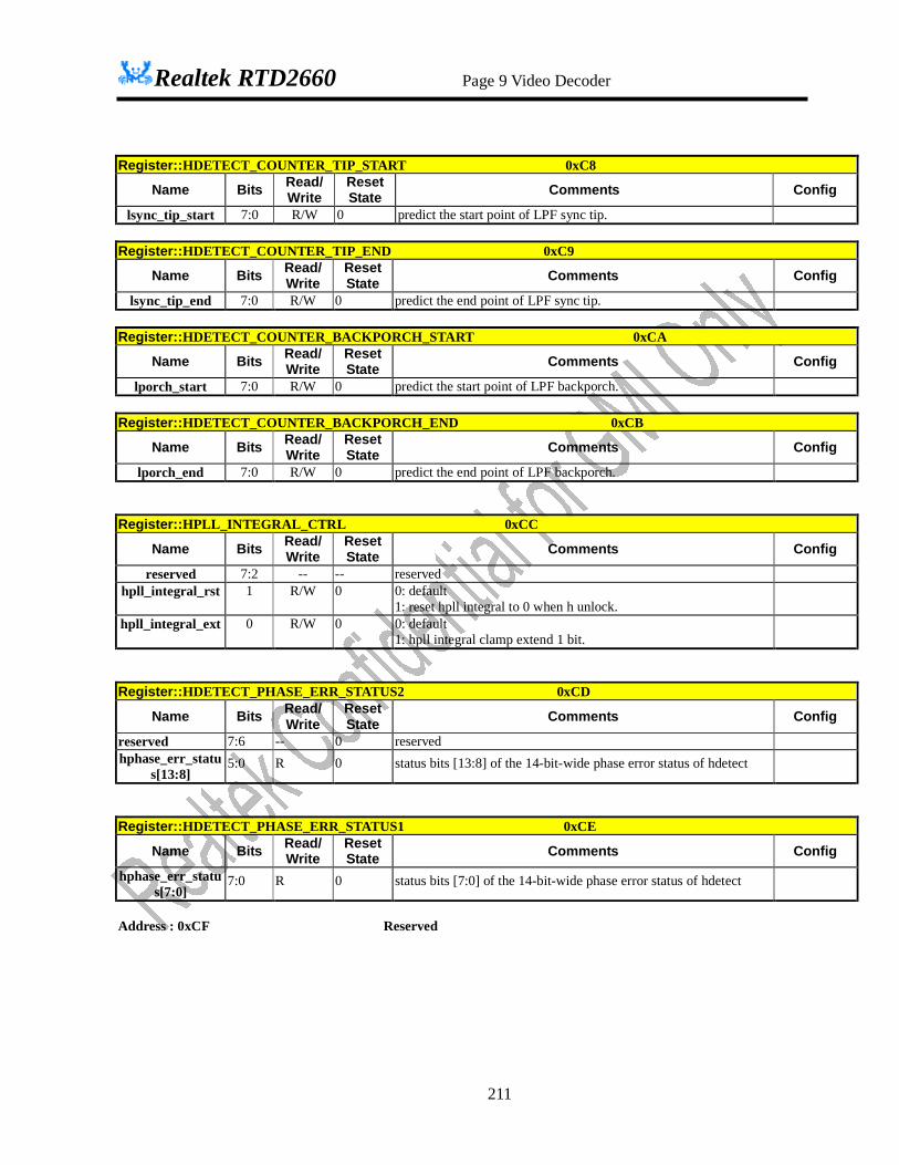
Realtek RTD2660 Page 9 Video Decoder
211
Register::HDETECT_COUNTER_TIP_START 0xC8
Name Bits Read/ Write
Reset State Comments Config
lsync_tip_start 7:0 R/W 0 predict the start point of LPF sync tip. Register::HDETECT_COUNTER_TIP_END 0xC9
Name Bits Read/ Write
Reset State Comments Config
lsync_tip_end 7:0 R/W 0 predict the end point of LPF sync tip. Register::HDETECT_COUNTER_BACKPORCH_START 0xCA
Name Bits Read/ Write
Reset State Comments Config
lporch_start 7:0 R/W 0 predict the start point of LPF backporch. Register::HDETECT_COUNTER_BACKPORCH_END 0xCB
Name Bits Read/ Write
Reset State Comments Config
lporch_end 7:0 R/W 0 predict the end point of LPF backporch. Register::HPLL_INTEGRAL_CTRL 0xCC
Name Bits Read/ Write
Reset State Comments Config
reserved 7:2 -- -- reserved hpll_integral_rst 1 R/W 0 0: default
1: reset hpll integral to 0 when h unlock.
hpll_integral_ext 0 R/W 0 0: default 1: hpll integral clamp extend 1 bit.
Register::HDETECT_PHASE_ERR_STATUS2 0xCD
Name Bits Read/ Write
Reset State Comments Config
reserved 7:6 -- 0 reserved hphase_err_statu
s[13:8] 5:0 R 0 status bits [13:8] of the 14-bit-wide phase error status of hdetect
Register::HDETECT_PHASE_ERR_STATUS1 0xCE
Name Bits Read/ Write
Reset State Comments Config
hphase_err_status[7:0]
7:0 R 0 status bits [7:0] of the 14-bit-wide phase error status of hdetect
Address : 0xCF Reserved

Realtek RTD2660 Page 9 Video Decoder
212
Horizontal Sync Detection Registers
Register::HSYNC_RISING 0xD0
Name Bits Read/ Write
Reset State Comments Config
hsync_rising 7:0 R/W 0x3E set the position of the expected hsync rising edge. The fine hsync detector uses it. The fine detector uses this time position to sample the video signal for the rising edge of the hsync.
Register::HSYNC_PHASE_OFFSET 0xD1
Name Bits Read/ Write
Reset State Comments Config
hsync_phase_offset
7:0 R/W 0x3E set the offset value between the coarse hsync detector and the fine hsync detector. Nominally set to 62. The course detector actually finds the middle of the hsync so we need to subtract the nominal hsync width to find the beginning of the hsync.
Register::HSYNC_GATE_START 0xD2
Name Bits Read/ Write
Reset State Comments Config
hsync_gate_start 7:0 R/W 0x00 These bits control the PLL horizontal sync detect window for coarse sync detection. This specifies the beginning of the window.
Register::HSYNC_GATE_END 0xD3
Name Bits Read/ Write
Reset State Comments Config
hsync_gate_end 7:0 R/W 0x80 control the PLL horizontal sync detect window for coarse sync detection. This specifies the end of the window.
Register::HSYNC_TIP_START 0xD4
Name Bits Read/ Write
Reset State Comments Config
hsync_tip_start 7:0 R/W 0xE9 control the PLL horizontal sync tip detect window used for AGC control. This specifies the beginning of the window. (default: -23)
Register::HSYNC_TIP_END 0xD5
Name Bits Read/ Write
Reset State Comments Config
hsync_tip_end 7:0 R/W 0x0F control the PLL horizontal sync tip detect window used for AGC control. This specifies the end of the window.
Register::HSYNC_RISING_START 0xD6
Name Bits Read/ Write
Reset State Comments Config
hsync_rising_start
7:0 R/W 0x2D a programmable start time of the window that looks for the rising edge of the hsync. This is used by the coarse hsync include.

Realtek RTD2660 Page 9 Video Decoder
213
Register::HSYNC_RISING_END 0xD7
Name Bits Read/ Write
Reset State Comments Config
hsync_rising_end 7:0 R/W 0x50 a programmable end time for the window which spans across the rising-edge of the horizontal sync pulse.
Register::BACKPROCH_START 0xD8
Name Bits Read/ Write
Reset State Comments Config
backporch_start 7:0 R/W 0x22 control the backporch detect window. This specifies the beginning of the window.
Register::BACKPORCH_END 0xD9
Name Bits Read/ Write
Reset State Comments Config
backporch_end 7:0 R/W 0x4E control the backproch detect window. This specifies the end of the window.
Register::HBLANK_START 0xDA
Name Bits Read/ Write
Reset State Comments Config
hblank_start 7:0 R/W 0xD6 specify the beginning of the horizontal-blank-interval window. (df=-42)
Register::HBLANK_END 0xDB
Name Bits Read/ Write
Reset State Comments Config
hblank_end 7:0 R/W 0x4E specify the end of the horizontal-blank-interval window. Register::BURST_GATE_START 0xDC
Name Bits Read/ Write
Reset State Comments Config
burst_gate_start 7:0 R/W 0x32 specify the beginning of the burst gate window. Note that this window is set to be bigger than the burst. The automatic burst position tracker finds the burst within this window.
Register::BURST_GATE_END 0xDD
Name Bits Read/ Write
Reset State Comments Config
burst_gate_end 7:0 R/W 0x46 specify the end of the burst gate window. Register::HACTIVE_START 0xDE
Name Bits Read/ Write
Reset State Comments Config
hactive_start 7:0 R/W 0x82 control the active video line time interval. This specifies the beginning of active line. This register is used to center the

Realtek RTD2660 Page 9 Video Decoder
214
horizontal position, and should not be used to crop the image to a smaller size.
Register::HACTIVE_WIDTH 0xDF
Name Bits Read/ Write
Reset State Comments Config
hactive_width 7:0 R/W 0x50 control the active video line time interval. This specifies the width of the active line, and should not be used to crop the image to a smaller size. The value 640 is added to this register.
Vertical Sync and Field Detection Registers
Register::VACTIVE_START 0xE0
Name Bits Read/ Write
Reset State Comments Config
vactive_start 7:0 R/W 0x22 control the first active video line in a field. This specifies the number of half-lines from the start of a field.
Register::VACTIVE_HEIGHT 0xE1
Name Bits Read/ Write
Reset State Comments Config
vactive_height 7:0 R/W 0x61 control the active video height. This specifies the height by the number of half lines. The value “384” is added to this register.
Register::VSYNC_H_MIN 0xE2
Name Bits Read/ Write
Reset State Comments Config
reserved 7 -- -- Reserved. vsync_h_min 6:0 R/W 0x70 defines the number of half-lines before the vsync that the hsync
detector circuit is disabled. This is to make sure that the HPLL is not confused by the equalization pulses and the broad pulses. Also in VCR trick modes the VSYNC is just one 3 line wide pulse with no hsync structure so it must be ignored.
Register::VSYNC_H_MAX 0xE3
Name Bits Read/ Write
Reset State Comments Config
Reserved 7 -- -- Reserved. vsync_h_max 6:0 R/W 0x0E defines the number of half_lines after the vsync that the hsync
detector circuit is re-enabled.
Register::VSYNC_VBI_MIN 0xE4
Name Bits Read/ Write
Reset State Comments Config
Reserved 7 -- -- Reserved. vsync_vbi_min 6:0 R/W 0x70 defines the number of half-lines before the VSYNC that VBI data is
valid. (df: -16)

Realtek RTD2660 Page 9 Video Decoder
215
Register::VSYNC_VBI_LOCKOUT_END 0xE5
Name Bits Read/ Write
Reset State Comments Config
vlock_wide_range
7 R/W 0 controls whether a wide or a narrow vertical locking range should be used.
vsync_vbi_max 6:0 R/W 0x0E defines the number of half-lines after the VSYNC that VBI data is valid.

Realtek RTD2660 Page 9 Video Decoder
216
VSYNC PLL Registers
Register::VSYNC_CNTL 0xE6
Name Bits Read/ Write
Reset State Comments Config
vsync_cntl 7:6 R/W 0 set the vsync output mode. 00: output the vertical PLL sync, except during VCR trick modes when the directly detected vsync is used 01: output the directly detected vsync. 10: output the vertical PLL derived vsync 11: output the PLL vsync in alternate mode
vsync_threshold 5:0 R/W 0 specifies a relative threshold to add to the slice level for the purpose of vsync detection.
Register::VSYNC_TIME_CONST 0xE7
Name Bits Read/ Write
Reset State Comments Config
field_polarity 7 R/W 0 sets the output field polarity. 0: field=1 for odd, field = 0 for even fields 1: field=0 for odd, field = 1 for even fields
flip_field 6 R/W 0 flips even/odd fields. veven_delayed 5 R/W 0 delays detection of even fields by 1 vertical line. vodd_delayed 4 R/W 0 delays detection of odd fields by 1 vertical line. field_detect_mode
3:2 R/W 0x02 control the field detection logic
vloop_tc3 1:0 R/W 0x02 set the vertical PLL time constant 3
00: 7/8
01: 15/16
10: 1
11: 1
Register::VSYNC_TIME_CONST2 0xE8
Name Bits Read/ Write
Reset State Comments Config
Reserved 7 -- -- reserved vloop_tc2 6:0 R/W 0x04 set the vertical PLL time constant 2(G2)
valid values: 0 ~ 64
Register::VSYNC_TIME_CONST1 0xE9
Name Bits Read/ Write
Reset State Comments Config
vloop_tc1 7:0 R/W 0x20 set the vertical PLL time constant 1(G1)
valid values: 0 ~ 128
Register::SERRATION_TH 0xEA
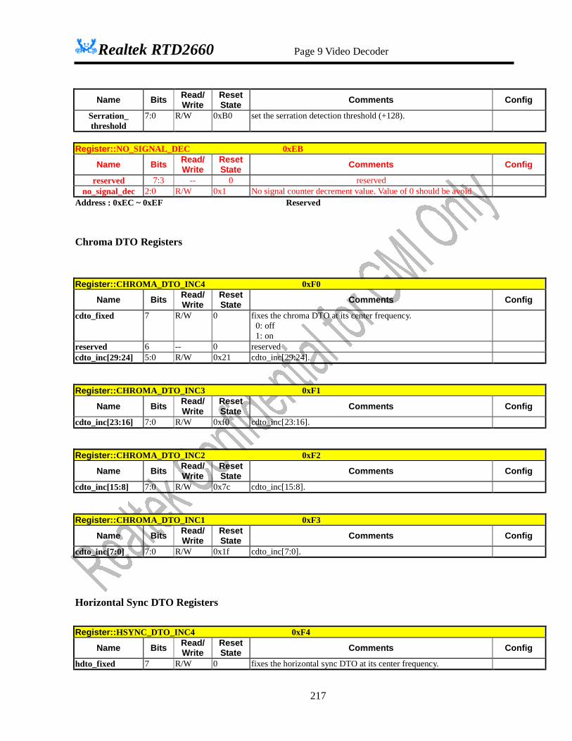
Realtek RTD2660 Page 9 Video Decoder
217
Name Bits Read/ Write
Reset State Comments Config
Serration_ threshold
7:0 R/W 0xB0 set the serration detection threshold (+128).
Register::NO_SIGNAL_DEC 0xEB
Name Bits Read/ Write
Reset State Comments Config
reserved 7:3 -- 0 reserved no_signal_dec 2:0 R/W 0x1 No signal counter decrement value. Value of 0 should be avoid
Address : 0xEC ~ 0xEF Reserved
Chroma DTO Registers
Register::CHROMA_DTO_INC4 0xF0
Name Bits Read/ Write
Reset State Comments Config
cdto_fixed 7 R/W 0 fixes the chroma DTO at its center frequency. 0: off 1: on
reserved 6 -- 0 reserved cdto_inc[29:24] 5:0 R/W 0x21 cdto_inc[29:24]. Register::CHROMA_DTO_INC3 0xF1
Name Bits Read/ Write
Reset State Comments Config
cdto_inc[23:16] 7:0 R/W 0xf0 cdto_inc[23:16]. Register::CHROMA_DTO_INC2 0xF2
Name Bits Read/ Write
Reset State Comments Config
cdto_inc[15:8] 7:0 R/W 0x7c cdto_inc[15:8]. Register::CHROMA_DTO_INC1 0xF3
Name Bits Read/ Write
Reset State Comments Config
cdto_inc[7:0] 7:0 R/W 0x1f cdto_inc[7:0].
Horizontal Sync DTO Registers
Register::HSYNC_DTO_INC4 0xF4
Name Bits Read/ Write
Reset State Comments Config
hdto_fixed 7 R/W 0 fixes the horizontal sync DTO at its center frequency.
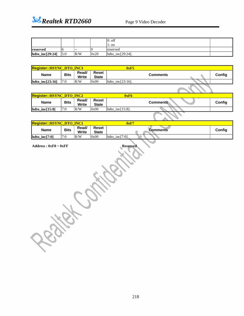
Realtek RTD2660 Page 9 Video Decoder
218
0: off 1: on
reserved 6 -- 0 reserved hdto_inc[29:24] 5:0 R/W 0x20 hdto_inc[29:24]. Register::HSYNC_DTO_INC3 0xF5
Name Bits Read/ Write
Reset State Comments Config
hdto_inc[23:16] 7:0 R/W 0x00 hdto_inc[23:16]. Register::HSYNC_DTO_INC2 0xF6
Name Bits Read/ Write
Reset State Comments Config
hdto_inc[15:8] 7:0 R/W 0x00 hdto_inc[15:8]. Register::HSYNC_DTO_INC1 0xF7
Name Bits Read/ Write
Reset State Comments Config
hdto_inc[7:0] 7:0 R/W 0x00 hdto_inc[7:0]. Address : 0xF8 ~ 0xFF Reserved

Realtek RTD2660 Page 9 Video Decoder
219
Auto Mode State Machine Table Status Registers
Register::auto_mode_table1 0xA0
Name Bits Read/ Write
Reset State Comments Config
table_cagc_en 7 R 0 table_vline_625 6 R 0
table_hpixel 5:4 R 0 table_ped 3 R 0
table_colour_mode
2:0 R 0
Register::auto_mode_table2 0xA1
Name Bits Read/ Write
Reset State Comments Config
table_hagc 7:0 R 0 Register::auto_mode_table3 0xA2
Name Bits Read/ Write
Reset State Comments Config
table_hactive_start
7:0 R 0
Register::auto_mode_table4 0xA3
Name Bits Read/ Write
Reset State Comments Config
table_vactive_start
7:0 R 0
Register::auto_mode_table5 0xA4
Name Bits Read/ Write
Reset State Comments Config
table_vactive_height
7:0 R 0
Register::auto_mode_table6 0xA5
Name Bits Read/ Write
Reset State Comments Config
reserved 7:6 -- -- table_cdto[29:24] 5:0 R 0 Register::auto_mode_table7 0xA6
Name Bits Read/ Write
Reset State Comments Config
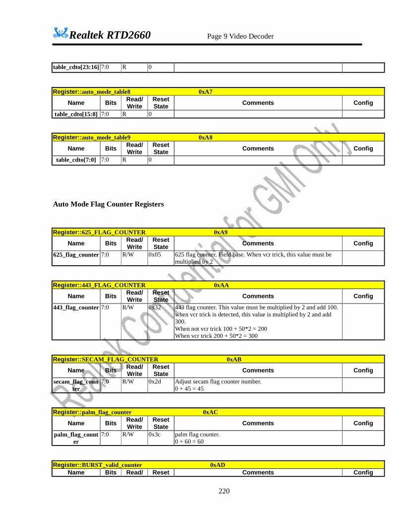
Realtek RTD2660 Page 9 Video Decoder
220
table_cdto[23:16] 7:0 R 0 Register::auto_mode_table8 0xA7
Name Bits Read/ Write
Reset State Comments Config
table_cdto[15:8] 7:0 R 0 Register::auto_mode_table9 0xA8
Name Bits Read/ Write
Reset State Comments Config
table_cdto[7:0] 7:0 R 0
Auto Mode Flag Counter Registers
Register::625_FLAG_COUNTER 0xA9
Name Bits Read/ Write
Reset State Comments Config
625_flag_counter 7:0 R/W 0x05 625 flag counter. Field base. When vcr trick, this value must be multiplied by 2
Register::443_FLAG_COUNTER 0xAA
Name Bits Read/ Write
Reset State Comments Config
443_flag_counter 7:0 R/W 0x32 443 flag counter. This value must be multiplied by 2 and add 100. when vcr trick is detected, this value is multiplied by 2 and add 300. When not vcr trick 100 + 50*2 = 200 When vcr trick 200 + 50*2 = 300
Register::SECAM_FLAG_COUNTER 0xAB
Name Bits Read/ Write
Reset State Comments Config
secam_flag_counter
7:0 R/W 0x2d Adjust secam flag counter number. 0 + 45 = 45
Register::palm_flag_counter 0xAC
Name Bits Read/ Write
Reset State Comments Config
palm_flag_counter
7:0 R/W 0x3c palm flag counter. 0 + 60 = 60
Register::BURST_valid_counter 0xAD
Name Bits Read/ Reset Comments Config

Realtek RTD2660 Page 9 Video Decoder
221
Write State Burst_valid_cou
nter 7:0 R/W 0x50 Burst magnitude not valid counter, when bigger than counter, burst
detect flag set 0. This value must be multiplied by 16 Default is 0 + 80*16 = 1280
Address : 0xAE ~ 0xAF Reserved

Realtek RTD2660 Page 9 Video Decoder
222
Auto Mode Flag Adjustment Registers
Register::MIDPOINT_ADJ 0xB0
Name Bits Read/ Write
Reset State Comments Config
midpoint_adjustment
7:0 R/W 0x00 Midpoint value minus this value is the final midpoint value
Register::freq_flag_threshold 0xB1
Name Bits Read/ Write
Reset State Comments Config
Freq_flag_threshold_tune
7:0 R/W 0x00 When 443 Mhz or secam setting﹐change 443 flag threshold toward positive direction. 160+0=160, 100+x=100.
Register::FREQ_VALID_MAX 0xB2
Name Bits Read/ Write
Reset State Comments Config
frequency_valid_upper_limit
7:0 R/W 0xc0 Upper limit for reasonable frequency value. When secam is set, this value must be multiplied by 2 and add 400. When secam is not set, this value must add 800. Secam, 400 + 160*2 = 720, Not secam, 800 + 160*1 = 960
Register::FREQ_VALID_INNER 0xB3
Name Bits Read/ Write
Reset State Comments Config
condition_enable 7 R/W 0 Enable frequency invalid condition. 0: disable 1: enable
frequency_valid_inner_limit
6:0 R/W 0x42 Inner limit for reasonable frequency value from +-300(250 when secam). When secam is set, this value must be multiplied by 2. When secam is set, 0 + 66*1 = 66, When secam is not set, 0 + 66*2 = 132,
Register::FREQ_VALID_MIN 0xB4
Name Bits Read/ Write
Reset State Comments Config
frequency_valid_lower_limit
7:0 R/W 0x50 Upper limit for reasonable frequency value. This value must be multiplied by 2 and add 100. 100 + 80*2 = 260
Register::SECAM_FLAG_COUNTER_MAX 0xB5
Name Bits Read/ Write
Reset State Comments Config
secam_flag_freq 7:0 R/W 0xa0 Secam flag counter upper condition for frequency offset. This

Realtek RTD2660 Page 9 Video Decoder
223
uency_upper_limit
value must be multiplied by 2. 160*2 = 320. (+-320)
Register::SECAM_FLAG_COUNTER_MIN 0xB6
Name Bits Read/ Write
Reset State Comments Config
secam_flag_frequency_lower_lim
it
7:0 R/W 0x0d Secam flag counter lower condition for frequency offset.
Register::palm_flag_phase_adj 0xB7
Name Bits Read/ Write
Reset State Comments Config
palm_flag_phase_adjust
7:0 R/W 0x80 palm flag phase adjustment.
Register::BURST_LOWER_LIMIT 0xB8
Name Bits Read/ Write
Reset State Comments Config
Burst_mag_trigger
7:4 R/W 0x02 When burst flag is from 1 to 0, threshold must be added by
this value.
Burst_mag_threshold
3:0 R/W 0x04 When input burst is smaller than this threshold, burst not valid
counter add 1.
Register::BURST_MAG_CHOICE 0xB9
Name Bits Read/ Write
Reset State Comments Config
vsync_select 7 R/W 1 select vsync signal. 0: vsync_l 1: vsync_vbi
secam_frequency_valid_enable
6 R/W 1 Enable valid_frequency_condition for secam counter. 0: disable 1: enable
reserved 5 - - reserved Burst_noise_wei
ghting_auto 4 R/W 1
Burst_noise_weighting
3:0 R/W 8 Noise weighting factor for burst flag threshold. Use this value is bit 4 is 0. 0 : 2/16 1 : 4/16 2 : 6/16 3 : 7/16 4 : 8/16 5 : 9/16 6 : 10/16 7 : 11/16 8 : 12/16
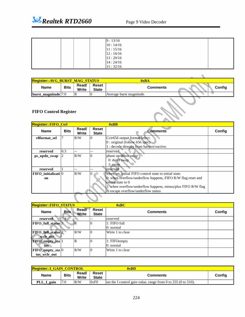
Realtek RTD2660 Page 9 Video Decoder
224
9 : 13/16 10 : 14/16 11 : 15/16 12 : 16/16 13 : 20/16 14 : 24/16 15 : 32/16
Register::AVG_BURST_MAG_STATUS 0xBA
Name Bits Read/ Write
Reset State Comments Config
burst_magnitude 7:0 R 0 Average burst magnitude.
FIFO Control Register
Register::FIFO_Ctrl 0xBB
Name Bits Read/ Write
Reset State Comments Config
v8format_sel 7 R/W 0 Ccir656 output format select. 0 : original (follow 656 spec) 1 : decode directly from hactive/vactive.
reserved 6:3 -- -- reserved ps_updn_swap 2 R/W 0 phase up/down swap
0: don’t swap 1: swap
reserved 1 -- -- reserved FIFO_initializati
on 0 R/W 0 when set, initial FIFO control state to initial state.
0: when overflow/underflow happens, FIFO R/W flag reset and return state to 0 1: when overflow/underflow happens, minus/plus FIFO R/W flag to escape overflow/underflow status
Register::FIFO_STATUS 0xBC
Name Bits Read/ Write
Reset State Comments Config
reserved 7:4 -- -- reserved FIFO_full_status 3 R 0 1: FIFO full
0: normal
FIFO_full_status_wclr_out
2 R/W 0 Wirte 1 to clear
FIFO_empty_status
1 R 0 1: FIFOempty 0: normal
FIFO_empty_status_wclr_out
0 R/W 0 Wirte 1 to clear
Register::I_GAIN_CONTROL 0xBD
Name Bits Read/ Write
Reset State Comments Config
PLL_I_gain 7:0 R/W 0xF0 set the I control gain value, range from 0 to 255 (0 to 510).

Realtek RTD2660 Page 9 Video Decoder
225
Register::MISC_CONTROL 0xBE
Name Bits Read/ Write
Reset State Comments Config
swallow_on_vsync
7 R/W 0 limit the swallow circuit actions only during V-sync blanking region. 0: disable 1: enable
ndivload_en 6 R/W 1 phase swallow divider load control enable. 0: disable 1: enable
ps_up_en 5 R/W 1 phase swallow up control enable. 0: disable 1: enable
ps_dn_en 4 R/W 1 phase swallow down control enable. 0: disable 1: enable
PLL_div 3:0 R/W 0xF set the divider parameter, range from 0 to 15 (2^0 to 2^15). Register::FIFO_DEPTH_MIN_STATUS 0xBF
Name Bits Read/ Write
Reset State Comments Config
reserved 7 -- -- reserved FIFO_depth_mi
n_clr 6 R/W 0 Wirte 1 to clear
FIFO_depth_min_status
5:0 R 0x00 the minimal depth of FIFO after the last read.
Register::FIFO_DEPTH_MAX_STATUS 0xC0
Name Bits Read/ Write
Reset State Comments Config
reserved 7 -- -- reserved FIFO_depth_ma
x_clr 6 R/W 0 Wirte 1 to clear
FIFO_depth_max_status
5:0 R 0x00 the maximum depth of FIFO after the last read..
Register::HSYNC_PULSE_START 0xC1
Name Bits Read/ Write
Reset State Comments Config
hsync_start 7:0 R/W 0x00 set the hsync start position after the trailing of hactive signal (pixels).
Register::HSYNC_PULSE_WIDTH 0xC2
Name Bits Read/ Write
Reset State Comments Config
hsync_width 7:0 R/W 0x40 set the hsync width (pixels). Register::CHROMA_HRESAMPLER_CONTROL 0xC3
Name Bits Read/ Write
Reset State Comments Config
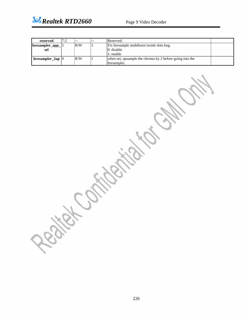
Realtek RTD2660 Page 9 Video Decoder
226
reserved 7:2 -- -- Reserved. hresampler_app_
sel 1 R/W 1 Fix hresample multiburst twinle dots bug.
0: disable 1: enable
hresampler_2up 0 R/W 1 when set, upsample the chroma by 2 before going into the hresampler.

Realtek RTD2660 Page 9 Video Decoder
227
SECAM Control Registers
Register::SECAM_Ctrl 0xC4
Name Bits Read/ Write
Reset State Comments Config
drdb_freq_const 7 R/W 1 for abnormal secam mode, use fixed frequency offset for compensation. 0: auto tracking 1: fixed frequency. Use dr_offset & db_offset value.
Drdb_vlpf_en 6 R/W 0 SECAM DrDb vertical LPF enable. 1: enable 0: disable.
reserved 5:2 -- -- Reserved. Secam_notch_filter
1:0 R/W 2 SECAM notch filter selection 00 : FIR filter 01 : iir filter with BW=0.7 10 : iir filter with BW=0.5 11 : iir filter with BW=0.4
Register::SECAM_Drfreq_offset 0xC5
Name Bits Read/ Write
Reset State Comments Config
Dr_offset 7:0 R/W 0x41 This value is used to fine tune the secam black level DR value. Default = 65
Register::SECAM_Dbfreq_offset 0xC6
Name Bits Read/ Write
Reset State Comments Config
Db_offset 7:0 R/W 0x14 This value is used to fine tune the secam black level DB value. Default = 20
Register::SECAM_hcount_reset_ctrl 0xC7
Name Bits Read/ Write
Reset State Comments Config
secam_phase_diff_hcount_en
7 R/W 0 Secam phase_diff_hcount_en enable 0: disable 1: enable
secam_phase_diff_hcount
6:0 R/W 0x00 If hcount < this value, the phase difference from cordic will reset to secam_phase_diff_dr/db.
Register::Phase_diff_dr_rst 0xC8
Name Bits Read/ Write
Reset State Comments Config
secam_phase_diff_dr
7:0 R/W 0xAB Secam dr’s phase diff from cordic reset value Default = ABh

Realtek RTD2660 Page 9 Video Decoder
228
Register::Phase_diff_db_rst 0xC9
Name Bits Read/ Write
Reset State Comments Config
Secam_phase_diff_db
7:0 R/W 0x14 Secam db’s phase diff from cordic reset value Default = 14h
Register::DrDb_gain_table_ctrl 0xCA
Name Bits Read/ Write
Reset State Comments Config
secam_gain_drdb_en
7 R/W 0 Secam gain drdb look up table enable 0: disable 1: enable
secam_gain_drdb 6:0 R/W 0 Drdb threshold. Register::Y_gain_table_ctrl 0xCB
Name Bits Read/ Write
Reset State Comments Config
secam_gain_y_en 7 R/W 0 Secam gain y look up table enable 0: disable 1: enable
secam_gain_y 6:0 R/W 8 Y threshold. Register::secam_gain_dly 0xCC
Name Bits Read/ Write
Reset State Comments Config
reserved 7:5 -- -- reserved Secam_gain_delay
4:0 R/W 0x12 Secam Y delay for dr/db gain
Register::SECAM_gain_table_debug 0xCD
Name Bits Read/ Write
Reset State Comments Config
secam_gain_debug_en
7 R/W 0 Secam gain debug enable 0: disable 1: enable
secam_gain_debug
6:0 R 0 Gain value read from the gain table
Address: 0xCE ~ 0xCF Reserved
MISC Control Registers
Register::LDPAUSE_CTRL 0xD0
Name Bits Read/ Write
Reset State Comments Config
Ld_pause_detect 7 R 0 LD pause detected. 0: normal play. 1: LD pause detected.
Ldp_det_en 6 R/W 1 Enable LD pause detect 0: disable.

Realtek RTD2660 Page 9 Video Decoder
229
1: enable. Ldp_switch_en 5 R/W 1 Enable 2D/3D switch when LD pause detected.
0: disable.(only detect, not switch) 1: auto switch to 2D if LD pause detected.
ldpaus_th 4:0 R/W 0x04 The threshold is this value multiply by 32. Register::VCR_OPTION 0xD1
Name Bits Read/ Write
Reset State Comments Config
Coch_en 7 R/W 0 Vlpf on lpfhsyncs enable for Co_channel. 1: enable 0: disable.
reserved 6:3 -- -- reserved lock_h_on_no_sig
nal 2 R/W 0 enable to lock hsync when no signal occurs and blue screen is set.
0: free run when no signal occurs and blue screen is set. 1: enable to lock hsync when no signal occurs and blue screen is set.
disable_blue_screen_when_VCR
1 R/W 1 disable the blue screen mode when VCR is detected. 0: enable 1: disable
detect_vcr_when_h_unlock
0 R/W 1 enable to detect VCR when h sync is unlocked. 0: disable 1: enable
Register::CENABLE_LINE_COUNT 0xD2
Name Bits Read/ Write
Reset State Comments Config
cenable_line_count
7:0 R 0 cenable_line_count [7:0]
Register::MEASURE_FIRST_V_HI 0xD3
Name Bits Read/ Write
Reset State Comments Config
reserved 7:2 -- -- Reserved. V_1st_line [9:8] 1:0 R 0 V_1st_line [9:8]
Register::MEASURE_FIRST_V_LOW 0xD4
Name Bits Read/ Write
Reset State Comments Config
V_1st_line [7:0] 7:0 R 0 V_1st_line [7:0] Register::MEASURE_SECOND_V_HI 0xD5
Name Bits Read/ Write
Reset State Comments Config
reserved 7:2 -- -- Reserved. V_2nd_line [9:8] 1:0 R 0 V_2nd_line [9:8] Register::MEASURE_SECOND_V_LOW 0xD6
Name Bits Read/ Write
Reset State Comments Config

Realtek RTD2660 Page 9 Video Decoder
230
V_2nd_line [7:0] 7:0 R 0 V_2nd_line [7:0] Register::PORCH_HEIGHT_M 0xD7
Name Bits Read/ Write
Reset State Comments Config
reserved 7:5 -- -- Reserved. Porch_h[12:8] 4:0 R 0 porch_height_measure: MSB[12:8].
Register::PORCH_HEIGHT_L 0xD8
Name Bits Read/ Write
Reset State Comments Config
Porch_h[7:0] 7:0 R 0 porch_height_measure: LSB[7:0]. Register::Signal_STM_Control 0xD9
Name Bits Read/ Write
Reset State Comments Config
reserved 7:4 -- -- reserved. field_toggle_en 3 R/W 1 force field toggle when abnormal Input happens.
0: disable (force field signal to 0) 1: enable (original zoran mode)
reserved 2:0 -- -- reserved Register::CDETECT_PHASE_ERR_STATUS2 0xDA
Name Bits Read/ Write
Reset State Comments Config
reserved 7:6 -- 0 reserved cdet_phase_err_s
tatus[13:8] 5:0 R 0 status bits [13:8] of the 14-bit-wide phase error status of cdetect
Register::CDETECT_PHASE_ERR_STATUS1 0xDB
Name Bits Read/ Write
Reset State Comments Config
cdet_phase_err_status[7:0]
7:0 R 0 status bits [7:0] of the 14-bit-wide phase error status of cdetect
Macrovision Control Registers
Register::MV_DETECT_WINDOW 0xDC
Name Bits Read/ Write
Reset State Comments Config
Mv_window2_value
7:0 R/W 0x19 MacroVision detect window setting
Register::MV_BURSTGATE_START 0xDD
Name Bits Read/ Write
Reset State Comments Config
Ad_burst_gate_st 7:0 R/W 0x32 MacroVision burstgate detect window start time.

Realtek RTD2660 Page 9 Video Decoder
231
art Register::MV_BURSTGATE_END 0xDE
Name Bits Read/ Write
Reset State Comments Config
Ad_burst_gate_end
7:0 R/W 0x46 MacroVision burstgate detect window end time
Register::COLORSTRIPE_CONTROL 0xDF
Name Bits Read/ Write
Reset State Comments Config
reserved 7:3 -- -- reserved Cstripe_detect_control
2:0 R/W 0 Colorstripe control.
Debug Test
Register::DEBUG_MUX 0xE0
Name Bits Read/ Write
Reset State Comments Config
debug_test_enable
7 R/W 0 enable the debug mode. When set, disable the normal output and switch to internal signal. 0: disable 1: enable
debug_test 6:0 R/W 0 internal signal select for debug. 0x00: internal debug mode 0x01: internal video 16 output 0x02: ADC input test mode 0x03: 4fsc data mode 0x04: phase error mode 0x05: mode detect debug mode(1) 0x06: mode detect debug mode(2) 0x07: mode detect debug mode(3) 0x08: mode detect debug mode(4) 0x09: mode detect debug mode(5) 0x0a: HPLL debug mode 0x0b: Interrupt debug mode 0x0c: ADC12 output mode 0x0d: ADC12 control mode 0x0e: PLL output mode 0x0f: PLL control mode 0x10: FIFO output mode others : reserved
Register::VIDEO_DEBUG_ANALOG 0xE1
Name Bits Read/ Write
Reset State Comments Config
muxanalogB 7:4 R/W 0 control the data sent to the analog DAC test point B. muxanalogA 3:0 R/W 0 control the data sent to the analog DAC test point A. Register::VIDEO_DEBUG_DIGITAL 0xE2

Realtek RTD2660 Page 9 Video Decoder
232
Name Bits Read/ Write
Reset State Comments Config
reserved 7:4 -- -- reserved muxdigital 3:0 R/W 0 control the data path sent to the digital test point. Register::BIST_TEST1 0xE3
Name Bits Read/ Write
Reset State Comments Config
bist_mode 7 R/W 0 Sram Bist mode start. bist_rst_n 6 R/W 1 Bist reset. reserved 5:0 -- --
Register::BIST_TEST2 0xE4
Name Bits Read/ Write
Reset State Comments Config
reserved 7:6 -- -- Reserved bist_done 5 R 0 bist_fail_0 4 R 0 bist_fail_1 3 R 0 bist_fail_2 2 R 0 bist_fail_3 1 R 0 bist_fail_4 0 R 0
Address : 0xE5 Reserved Register::PATTERN_CONTROL 0xE6
Name Bits Read/ Write
Reset State Comments Config
ad1_dma_en 7 R/W 0 AD1 input from DMA1. 1: From DMA1. 0: From ADC1.
ad2_dma_en 6 R/W 0 AD2 input from DMA2. 1: From DMA2. 0: From ADC2.
reserved 5:3 -- -- Reserved. crc_chk_sel 2 R/W 0 0: for QC
1: for MP
pattern_gen_cvbs_mode
1 R/W 0 0: NTSC 1: PAL-I
pattern_generator_enable
0 R/W 0 enable the pattern generator.
Note: CRC generator polynomial: X^32+X^26+X^23+X^22+X^16+X^12+X^11+X^10+X^8+X^7+X^5+X^4+X^2+X+1 Register::CRC_RESULT2 0xE7
Name Bits Read/ Write
Reset State Comments Config
reserved 7:4 -- -- Reserved. CRC_result_2 3:0 R 0 CRC check result: hi byte (19:16).
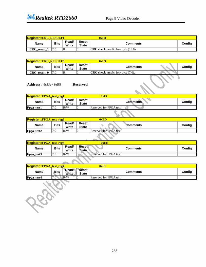
Realtek RTD2660 Page 9 Video Decoder
233
Register::CRC_RESULT1 0xE8
Name Bits Read/ Write
Reset State Comments Config
CRC_result_1 7:0 R 0 CRC check result: low byte (15:8). Register::CRC_RESULT0 0xE9
Name Bits Read/ Write
Reset State Comments Config
CRC_result_0 7:0 R 0 CRC check result: low byte (7:0). Address : 0xEA ~ 0xEB Reserved Register::FPGA_test_reg1 0xEC
Name Bits Read/ Write
Reset State Comments Config
Fpga_test1 7:0 R/W 0 Reserved for FPGA test. Register::FPGA_test_reg2 0xED
Name Bits Read/ Write
Reset State Comments Config
Fpga_test2 7:0 R/W 0 Reserved for FPGA test. Register::FPGA_test_reg3 0xEE
Name Bits Read/ Write
Reset State Comments Config
Fpga_test3 7:0 R/W 0 Reserved for FPGA test. Register::FPGA_test_reg4 0xEF
Name Bits Read/ Write
Reset State Comments Config
Fpga_test4 7:0 R/W 0 Reserved for FPGA test.

Realtek RTD2660 Page 9 Video Decoder
234
ADC Clamping Test Mode
Register::clamp_test_reg0 0xF0
Name Bits Read/ Write
Reset State Comments Config
C_blevel[7:0] 7:0 R 0 The blank level of red or Pr signal. Bit 7 to bit 0. Register::clamp_test_reg1 0xF1
Name Bits Read/ Write
Reset State Comments Config
reserved 7:4 -- -- reserved C_blevel[11:8] 3:0 R 0 The blank level of red or Pr signal. Bit 11 to bit 8. Register::clamp_test_reg6 0xF2
Name Bits Read/ Write
Reset State Comments Config
Comp_blevel[7:0] 7:0 R 0 The blank level of composite or Y signal. Bit 7 to bit 0. Register::clamp_test_reg7 0xF3
Name Bits Read/ Write
Reset State Comments Config
reserved 7:4 -- -- reserved Comp_blevel[11:8]
3:0 R 0 The blank level of composite or Y signal. Bit 11 to bit 8.
Register::clamp_test_reg8 0xF4
Name Bits Read/ Write
Reset State Comments Config
Comp_slevel[7:0] 7:0 R 0 The sync level of composite or Y signal. Bit 7 to bit 0. Register::clamp_test_reg9 0xF5
Name Bits Read/ Write
Reset State Comments Config
reserved 7:4 -- -- reserved Comp_slevel[11:8]
3:0 R 0 The sync level of composite or Y signal. Bit 11 to bit 8.
Register::clamp_test_reg10 0xF6
Name Bits Read/ Write
Reset State Comments Config
ADC1_Voffset[7:0]
7:0 R/W 0 The Voltage offset setting for ADC1. Bit 7 to bit 0.
Register::clamp_test_reg11 0xF7
Name Bits Read/ Reset Comments Config
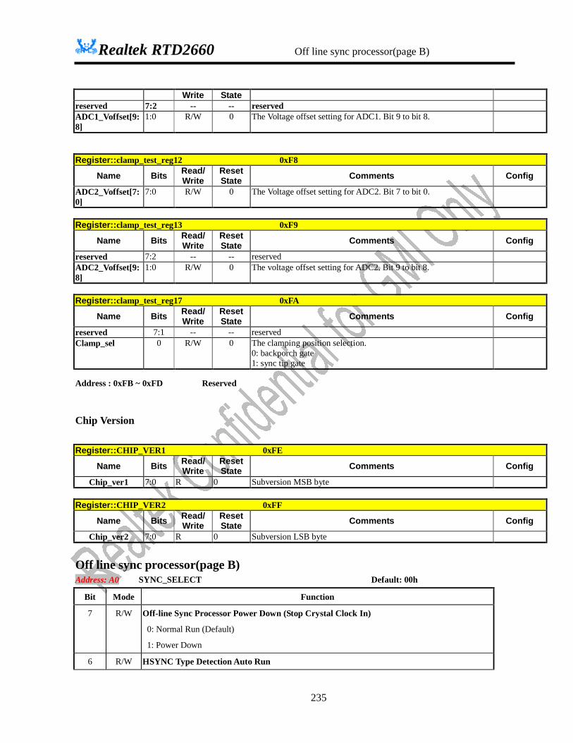
Realtek RTD2660 Off line sync processor(page B)
235
Write State reserved 7:2 -- -- reserved ADC1_Voffset[9:8]
1:0 R/W 0 The Voltage offset setting for ADC1. Bit 9 to bit 8.
Register::clamp_test_reg12 0xF8
Name Bits Read/ Write
Reset State Comments Config
ADC2_Voffset[7:0]
7:0 R/W 0 The Voltage offset setting for ADC2. Bit 7 to bit 0.
Register::clamp_test_reg13 0xF9
Name Bits Read/ Write
Reset State Comments Config
reserved 7:2 -- -- reserved ADC2_Voffset[9:8]
1:0 R/W 0 The voltage offset setting for ADC2. Bit 9 to bit 8.
Register::clamp_test_reg17 0xFA
Name Bits Read/ Write
Reset State Comments Config
reserved 7:1 -- -- reserved Clamp_sel 0 R/W 0 The clamping position selection.
0: backporch gate 1: sync tip gate
Address : 0xFB ~ 0xFD Reserved
Chip Version
Register::CHIP_VER1 0xFE
Name Bits Read/ Write
Reset State Comments Config
Chip_ver1 7:0 R 0 Subversion MSB byte Register::CHIP_VER2 0xFF
Name Bits Read/ Write
Reset State Comments Config
Chip_ver2 7:0 R 0 Subversion LSB byte
Off line sync processor(page B) Address: A0 SYNC_SELECT Default: 00h
Bit Mode Function
7 R/W Off-line Sync Processor Power Down (Stop Crystal Clock In)
0: Normal Run (Default)
1: Power Down
6 R/W HSYNC Type Detection Auto Run

Realtek RTD2660 Off line sync processor(page B)
236
0: manual (Default)
1: automatic
5 R/W De-composite circuit enable
0: Disable (Default)
1: Enable
4 R/W Input Sync. Source selection
0: HS_RAW(SS/CS) (Default)
1: SOG/SOY
3:2 R/W Input Sync. Source is HS_RAW, CR.A0[4] = 0
2’bx0: AHS0/AVS0 (Default)
2’bx1: AHS1/AVS1
Input Sync. Source is SOG, CR.A0[4] = 1.
2’b00: VGA-SOG0 (Default)
2’b01: VGA-SOG1
2’b1x: Video-ADC SOG
1 R/W Reserved to 0.
0 R/W HSYNC & VSYNC Measured Mode
0: HS period counted by crystal clock & VS period counted by HS (Analog mode) (Default)
1: H resolution counted by input clock & V resolution counted by ENA (Digital mode)
(Get the correct resolution which is triggered by enable signal, ENA)
Address: A1 SYNC_INVERT Default: 00h
Bit Mode Function
7 R/W COAST Signal Invert Enable:
0: Not inverted (Default)
1: Inverted
6 R/W COAST Signal Output Enable:
0: Disable (Default)
1: Enable
5 R/W HS_OUT Signal Invert Enable:
0: Not inverted (Default)
1: Inverted
4 R/W HS_OUT Signal Output Enable:
0: Disable (Default)
1: Enable
3 R/W CS_RAW Inverted Enable
0: Normal (Default)

Realtek RTD2660 Off line sync processor(page B)
237
1: Invert
2 R/W CLAMP Signal Output Enable
0: Disable (Default)
1: Enable
1 R/W HS Masked in Coast
0: Disable (Default) (SS/SOY)
1: Enable (CS or SOG ) 0 R/W Reserved to 0
Address: A2 SYNC_CTRL (SYNC Control Register) Default: 06h
Bit Mode Function 7 R/W Reserved to 0
6 R/W Select HS_OUT Source Signal
0: Bypass (SeHs)(Use in Separate Mode)
1: Select De-Composite HS out(DeHs) (In Composite mode)
5 R/W Select ADC_VS Source Signal (Auto switch in Auto Run Mode)
0: VS_RAW
1: DeVS
4 R/W CLK Inversion to latch ADC HS for Clamp
0: Non Inversion (Default)
1: Inversion
3 R/W Inversion of HSYNC to measure VSYNC
0: Non Inversion (Default)
1: Inversion
2 R/W HSYNC Measure Source(ADC_HS1)
0: Select ADC_HS
1: Select SeHS or DeHS by CR49[6] (Default)
1:0 R/W Measure HSYNC/VSYNC Source Select:
00: Reserved
01: VIDEO8 / VIDEO16
10: ADC_HS1/ADC_VS (Default)
11: CS_RAW/VS_RAW
Address: A3 STABLE_HIGH_PERIOD_H Default: 00h
Bit Mode Function
7 R Even/Odd Field of YPbPr (By Line-Count Mode)
0: Even
1: Odd
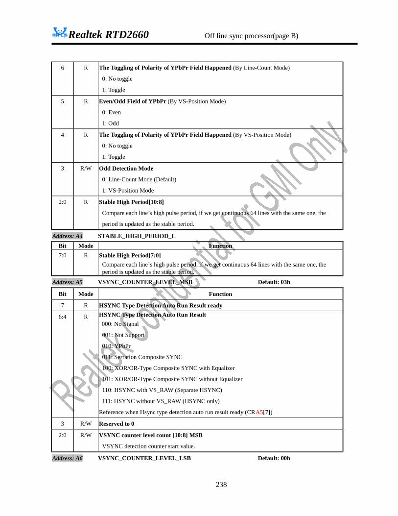
Realtek RTD2660 Off line sync processor(page B)
238
6 R The Toggling of Polarity of YPbPr Field Happened (By Line-Count Mode)
0: No toggle
1: Toggle
5 R Even/Odd Field of YPbPr (By VS-Position Mode)
0: Even
1: Odd
4 R The Toggling of Polarity of YPbPr Field Happened (By VS-Position Mode)
0: No toggle
1: Toggle
3 R/W Odd Detection Mode
0: Line-Count Mode (Default)
1: VS-Position Mode
2:0 R Stable High Period[10:8]
Compare each line’s high pulse period, if we get continuous 64 lines with the same one, the
period is updated as the stable period.
Address: A4 STABLE_HIGH_PERIOD_L Bit Mode Function 7:0 R Stable High Period[7:0]
Compare each line’s high pulse period, if we get continuous 64 lines with the same one, the period is updated as the stable period.
Address: A5 VSYNC_COUNTER_LEVEL_MSB Default: 03h
Bit Mode Function
7 R HSYNC Type Detection Auto Run Result ready
6:4 R HSYNC Type Detection Auto Run Result 000: No Signal
001: Not Support
010: YPbPr
011: Serration Composite SYNC
100: XOR/OR-Type Composite SYNC with Equalizer
101: XOR/OR-Type Composite SYNC without Equalizer
110: HSYNC with VS_RAW (Separate HSYNC)
111: HSYNC without VS_RAW (HSYNC only)
Reference when Hsync type detection auto run result ready (CRA5[7]) 3 R/W Reserved to 0
2:0 R/W VSYNC counter level count [10:8] MSB
VSYNC detection counter start value.
Address: A6 VSYNC_COUNTER_LEVEL_LSB Default: 00h

Realtek RTD2660 Off line sync processor(page B)
239
Bit Mode Function
7:0 R/W VSYNC counter level count [7:0] LSB
Address: A7 HSYNC_TYPE_DETECTION_FLAG
Bit Mode Function
7 R HSYNC Overflow (16-bits)
6 R Stable Period Change (write clear when CRA7[6]=1 or CRA8[0]=1)
5 R Stable Polarity Change (write clear when CR A7 [5]=1 or CR A8 [0]=1)
4 R VS_RAW Edge Occurs (write clear when CR A7 [4]=1 or CR A8 [0]=1)
If VS_RAW edge occurs, this bit is set to “1”.
3 R Detect Capture Window Unlock Repeated 32 Times (write clear when CR A7 [3]=1 or CR A8
[0]=1)
2 R HSYNC with Equalization (write clear when CR A7 [2]=1 or CR A8 [0]=1)
1 R HSYNC Polarity Change (write clear when CR A7 [1]=1 or CR A8 [0]=1)
0 R Detect Capture Window Unlock (write clear when CR A7 [0]=1 or CR A8 [0]=1)
Address: A8 STABLE_MEASURE Default: 00h
Bit Mode Function
7 R Stable Flag
0: Period or polarity can’t get continuous stable status.
1: Both polarity and period are stable.
6 R Stable Polarity
0: Negative
1: Positive
Compare each line’s polarity; if we get continuous N 64 lines with the same one, the polarity is
updated as the stable polarity.
5:4 R/W Feedback HSYNC High Period Select by ADC Clock:
00: 32 (Default)
01: 64
10: 96
11: 128
3 R/W Stable Period Tolerance
0: ±2 crystal clks (Default)
1: ±4 crystal clks
2 R/W VSYNC measure invert Enable
0: Disable (Default)
1: Enable

Realtek RTD2660 Off line sync processor(page B)
240
1 R/W Pop Up Stable Value
0: No Pop Up (Default)
1: Pop Up Result, (CRA3[2:0], CRA4[7:0], CRA7[3], CRA9[2:0], CRAA[7:0])
0 R/W Stable Measure Start
0 : Stop (Default)
1 : Start
Address: A9 Stable_Period_H Default: 80h
Bit Mode Function
7 R Measure One Frame Status
0: Finished after 1 frame measuring / Measure finished
1: Measuring Now
6 R CS_RAW Inverted by Auto Run Mode
0: Not inverted
1: Inverted
5 R/W HS_OUT Bypass PLL into VGIP 0: Disable (Default) 1: Enable
4 R/W Reserved to 0
3 R/W ADC_VS Source Select in Test Mode
0: Select ADC_VS Source in Normal Mode or Auto Mode by CRA0[6] (Default)
1: Select ADC_VS Source in Test Mode (Select VS_RAW or DeVS by CRA2[5])
2:0 R Stable Period[10:8]
Compare each line’s period, if we get continuous 64 lines with the same one, the period is updated
as the stable period.
Address: AA Stable_Period_L
Bit Mode Function
7:0 R Stable Period[7:0]
Compare each line’s period, if we get continuous 64 lines with the same one, the period is updated
as the stable period.
Address: AB MEAS_HS_PER_H (HSYNC Period Measured Result) Default: 8’b000xxxxx
Bit Mode Function
7 R/W On Line Auto Measure Enable
0: Disable (Default)
1: Enable
6 R/W Pop Up Period Measurement Result
0: No Pop Up (Default)
1: Pop Up Result

Realtek RTD2660 Off line sync processor(page B)
241
5 R/W Start a HS & VS period / H & V resolution & polarity measurement (on line monitor)
0: Finished/Disable (Default)
1: Enable to start a measurement, auto cleared after finished
4 R Over-flow bit of Input HSYNC Period Measurement
0: No Over-flow occurred
1: Over-flow occurred
3:0 R Input HSYNC Period Measurement Result: High Byte[11:8]
Address: AC MEAS_HS_PER_L (HSYNC Period Measured Result)
Bit Mode Function
7:0 R Input HSYNC Period Measurement Result: Low Byte[7:0]
l The result is expressed as the average number of crystal clocks (CRA0[0]=0), or input clocks (CR47[0]=1)
between 2 HSYNC.
l The result is the total number of crystal/input clocks inside 16-HSYNC periods divided by 16.
l Fractional part of measure result is stored in CRAF[3:0].
Address: AD MEAS_VS_PER_H (VSYNC Period Measured Result)
Bit Mode Function
7 R Input VSYNC Polarity Indicator
0: negative polarity (high period is longer than low one)
1: positive polarity (low period is longer than high one)
6 R Input HSYNC Polarity Indicator
0: negative polarity (high period is longer than low one)
1: positive polarity (low period is longer than high one)
5 R Time-Out bit of Input VSYNC Period Measurement (No VSYNC occurred)
0: No Time Out
1: Time Out occurred
4 R Over-flow bit of Input VSYNC Period Measurement
0: No Over-flow occurred
1: Over-flow occurred
3:0 R Input VSYNC Period Measurement Result: High Byte[11:8]
Address: AE MEAS_VS_PER_L (VSYNC Period Measured Result)
Bit Mode Function
7:0 R Input VSYNC Period Measurement Result: Low Byte[7:0]
l This result is expressed in terms of input HS pulses.
l When measured digitally, the result is expressed as the number of input ENA signal within a frame.
Address: AF MEAS_HS&VS_HI_H (HSYNC&VSYNC High Period Measured Result)
Bit Mode Function

Realtek RTD2660 Off line sync processor(page B)
242
7:4 R Input HSYNC High Period Measurement Result: High Byte[11:8] (CRB1[0] = 0)
Input VSYNC High Period Measurement Result: High Byte[11:8] (CRB1[0] = 1)
3:0 R Input HSYNC Period Measurement Fractional Result (See CRAB,AC)
Address: B0 MEAS_HS&VS_HI_L (HSYNC&VSYNC High Period Measured Result)
Bit Mode Function
7:0 R Input HSYNC High Period Measurement Result: Low Byte[7:0] (CRB1[0] = 0)
Input VSYNC High Period Measurement Result: Low Byte[7:0] (CRB1[0] = 1)
l This result of HSYNC high-period is expressed in terms of crystal clocks. When measured digitally, the result of
HSYNC high-period is expressed as the number of input clocks inside the input enable signal.
l This result of VSYNC high-period is expressed in terms of input HS pulses
Address: B1 MEAS_HS&VS_HI_SEL (VSYNC High Period Measured Result) Default:00h
Bit Mode Function
7:6 R/W HSYNC_MAX_DELTA
00: Don’t care (CR B1 [3] will never go high)
01: 4-clock
10: 8-clock
11: 16-clock
5:4 R/W VSYNC_MAX_DELTA
00: Don’t care (CR B1 [2] will never go high)
01: 2-HSYNC
10: 4-HSYNC
11: 8-HSYNC
3 R HSYNC_OVER_RANGE
Set to 1 if variation of HSYNC larger than HSYNC_MAX_DELTA is detected by on-line
measurement (CR B1 [7]=1). Write to clear this flag.
2 R VSYNC_OVER_RANGE
Set to 1 if variation of VSYNC larger than VSYNC_MAX_DELTA is detected by on-line
measurement (CR52[7]=1). Write to clear this flag. 1 R/W Start Measurement after Mode Detection Auto-mode
0: Disable 1: Enable (Default)
0 R/W HSYNC/VSYNC High Period Measurement Result Select
0: HSYNC
1: VSYNC
(See CRAF~CR B0)
Address: B2 Reserved to 0
Address: B3 SYNC_TEST_MISC Default: 00h
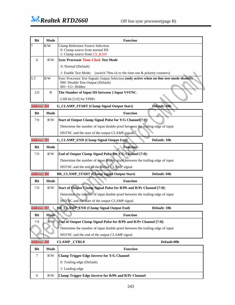
Realtek RTD2660 Off line sync processor(page B)
243
Bit Mode Function 7 R/W Clamp Reference Source Selection
0: Clamp source from normal HS 1: Clamp source from CS_RAW
6 R/W Sync Processor Time-Clock Test Mode
0: Normal (Default)
1: Enable Test Mode; (switch 70ns-ck to the time-out & polarity counters) 5:3 R/W Sync Processor Test Signals Output Selection (only active when on-line test-mode disable)
000: Disable Test-Output (Default) 001~111: Hidden
2:0 R The Number of Input HS between 2 Input VSYNC.
LSB bit [2:0] for YPbPr
Address: B4 G_CLAMP_START (Clamp Signal Output Start) Default: 04h
Bit Mode Function
7:0 R/W Start of Output Clamp Signal Pulse for Y/G Channel[7:0]:
Determine the number of input double-pixel between the trailing edge of input
HSYNC and the start of the output CLAMP signal.
Address: B5 G_CLAMP_END (Clamp Signal Output End) Default: 10h
Bit Mode Function
7:0 R/W End of Output Clamp Signal Pulse for Y/G Channel [7:0]:
Determine the number of input double-pixel between the trailing edge of input
HSYNC and the end of the output CLAMP signal.
Address: B6 BR_CLAMP_START (Clamp Signal Output Start) Default: 04h
Bit Mode Function
7:0 R/W Start of Output Clamp Signal Pulse for B/Pb and R/Pr Channel [7:0]:
Determine the number of input double-pixel between the trailing edge of input
HSYNC and the start of the output CLAMP signal.
Address: B7 BR_CLAMP_END (Clamp Signal Output End) Default: 10h
Bit Mode Function
7:0 R/W End of Output Clamp Signal Pulse for B/Pb and R/Pr Channel [7:0]:
Determine the number of input double-pixel between the trailing edge of input
HSYNC and the end of the output CLAMP signal.
Address: B8 CLAMP _CTRL0 Default:00h
Bit Mode Function
7 R/W Clamp Trigger Edge Inverse for Y/G Channel
0: Trailing edge (Default)
1: Leading edge
6 R/W Clamp Trigger Edge Inverse for B/Pb and R/Pr Channel

Realtek RTD2660 Off line sync processor(page B)
244
0: Trailing edge (Default)
1: Leading edge
5:0 R/W Mask Line Number before DeVS [5:0]
Address: B9 CLAMP _CTRL1 Default: 00h
Bit Mode Function
7 R/W Clamp Mask Enable
0: Disable (Default)
1: Enable
6 R/W Select Clamp Mask as De VS
0: Disable
1: Enable
5:0 R/W Mask Line Number after DeVS [5:0]
CRB8[5:0] and CRB9[5:0] will set number of Mask Line before/after DeVS for Clamp Mask.
Address: BA CLAMP_CTRL2 Default: 00h
Bit Mode Function
7 R/W Clamp Clock Source
0: ADC_Clock (Default)
1: Crystal Clock
6 R/W Clamp Counter Unit (CRB4~CRB7)
0: Double Pixels (Default)
1: Single Pixel
5 R/W Off-line ADC Clamp Enable
0: Disable (Default)
1: Enable
4 R/W Off-line ADC Selection
0: ADC-0 (Default)
1: ADC-1
3 R/W Off-Line ADC-3 Clamp Source
0: Clamp-G (Default)
1: Clamp-BR
3 R/W Off-Line ADC-2 Clamp Source
0: Clamp-G (Default)
1: Clamp-BR
3 R/W Off-Line ADC-1 Clamp Source
0: Clamp-G (Default)
1: Clamp-BR

Realtek RTD2660 Off line sync processor(page B)
245
3 R/W Off-Line ADC-0 Clamp Source
0: Clamp-G (Default)
1: Clamp-BR
Address: BB CLAMP_CTRL3 Default: 00h
Bit Mode Function
7 R/W Video-ADC-3 Clamp Output Enable
0: Disable (Default)
1: Enable
6 R/W Video-ADC-2 Clamp Output Enable
0: Disable (Default)
1: Enable
5 R/W Video-ADC-1 Clamp Output Enable
0: Disable (Default)
1: Enable
4 R/W Video-ADC-0 Clamp Output Enable
0: Disable (Default)
1: Enable
3 R/W Video-ADC-3 Clamp Source
0: Clamp-G (Default)
1: Clamp-BR
2 R/W Video-ADC-2 Clamp Source
0: Clamp-G (Default)
1: Clamp-BR
1 R/W Video-ADC-1 Clamp Source
0: Clamp-G (Default)
1: Clamp-BR
0 R/W Video-ADC-0 Clamp Source
0: Clamp-G (Default)
1: Clamp-BR
Address: BC COAST_CTRL Default: 21h
Bit Mode Function
7:4 R/W Start of COAST before DeVS Leading Edge [3:0]
3:0 R/W End of COAST after DeVS Trailing Edge [3:0]
Address: BD CAPTURE_WINDOW_SETTING Default: 04h
Bit Mode Function

Realtek RTD2660 Auto SOY(page B)
246
7 R/W Reserved to 0
6 R/W Capture Miss Limit during Hsync Extraction
0: 32 (Default)
1: 16
5 R/W Capture Window add step as Miss Lock
0: ±1 crystal clks (Default)
1: ±2 crystal clks
4:0 R/W Capture Window Tolerance 5’h00: ±6 crystal clks for capture window 5’h01 ~ 5’b1F : ±1 ~ ±31 crystal clks for capture window
Address: BE DETECTION_TOLERANCE_SETTING Default: 00h
Bit Mode Function
7 R/W Reserved to 0
6:5 R/W Stable Period Tolerance Extension
00: Use CRA8 [3] Setting (Default)
01: ±4 crystal clks
10: ±8 crystal clks
11: ±16 crystal clks
4:0 R/W H-sync for De-composite De-bounce Length 5’h00: Disable De-bounce Function (Default)
5’h01 ~ 5’h1F : De-bounce 1 ~ 31 crystal clks for de-composite
Address: BF Skip-Line Control Default: 00h
Bit Mode Function
7:4 R/W Skip Line[3:0]
Skip Lines after Vsync detected
3:0 R/W Reserved to 0
Auto SOY(page B) SOY Channel 0 // channel0 SOY auto compare level detect control Register0 Register::SOYCH0_CFG0 0xc0
Name Bits Read/Write
Reset State Comments Config
CH0_Delta 7:2 R/W 0x10 Delta value from detected lowest level for hsync
detecting
CH0_Digital_LPF 1:0 R/W 0x1 Digital LPF after ADC
00: 1 tap
01: 2 taps
10: 4 taps

Realtek RTD2660 Auto SOY(page B)
247
11: 4 taps
Register::SOYCH0_CFG1 0xc1
Name Bits Read/Write
Reset State Comments Config
CH0_DEBOUNCE_SE
L
7:5 R/W 0x4 Debounce Select
000 : No-debounce
001 : 2T debounce
010 : 3T debounce
…..
111 : 8T debounce
CH0_IE_E 4 R/W 0x0 Auto 1/2 sync level detect time out interrupt
enable
0: disable
1: enable
CH0_MLPF_MS 3:2 R/W 0x1 Moving average LPF mode select
00: 8 taps
01: 16 taps
10: 32 taps
others : 16 taps
CH0_ADC_LPF 1:0 R/W 0x2 Digital LPF BW select
00:2 points average filter
01:4 points average filter
10:8 points average filter
11:16 points average filter
default : 4 point average filter
// channel0 SOY auto compare level detect control Register1 Register::SOYCH0_CFG2 0xc2
Name Bits Read/Write
Reset State Comments Config
CH0_MODE 7 R/W 0x1 Auto 1/2 sync level detect mode
0: one shot
1: continue
CH0_OFFSET_V 6:0 R/W 0x0 offset value
SOY compare level=offset value+feedback
value
Bit 6 is sign bit

Realtek RTD2660 Auto SOY(page B)
248
Register::SOYCH0_CFG3 0xc3
Name Bits Read/Write
Reset State Comments Config
CH0_ENABLE 7 R/W 0x0 Auto 1/2 sync level detect enable/ disable
0: disable
1: enable
Reserved 6 -
CH0_M_CMPL 5:0 R/W 0x1E Compare level Manual setting
Only valid when CH0_CMPL_U_Sel set 0
Register::SOYCH0_CFG4 0xc4
Name Bits Read/Write
Reset State Comments Config
CH0_D_TIME 7:4 R/W 0x4 Compare level auto update delay time after 1/2
sync level latched for continue mode.
The Dealy Time Output Hsync DC Level for
Analog Issue.
CH0_CMPL_U_Sel 3 R/W 0 Compare level update source sel
0: Manual compare level
1: Auto compare level
CH0_U_mode 2 R/W 0x0 Compare level update mode
0: normal
1: step updating
CH0_U_step 1:0 R/W 0x0 compare level updating step
00:1/2 of sync DC_level(i)-DC_level(i-1)
01:1/4 of sync DC_level(i)-DC_level(i-1)
10:1/8 of sync DC_level(i)-DC_level(i-1)
11:1/16 of sync DC_level(i)-DC_level(i-1)
Register::SOYCH0_CFG5 0xc5
Name Bits Read/Write
Reset State Comments Config
Reserved 7:6 -
CH0_Min_diff 5:0 R/W 0x4 Minimum difference threshold to update
compare level
// channel0 SOY auto compare level detect control Register2 Register::SOYCH0_CFG6 0xc6
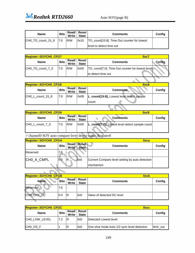
Realtek RTD2660 Auto SOY(page B)
249
Name Bits Read/Write
Reset State Comments Config
CH0_TO_count_15_8 7:0 R/W 0x10 TO_count[15:8], Time Out counter for lowest
level to detect time out
Register::SOYCH0_CFG7 0xc7
Name Bits Read/Write
Reset State Comments Config
CH0_TO_count_7_0 7:0 R/W 0x00 TO_count[7:0], Time Out counter for lowest level
to detect time out
Register::SOYCH0_CFG8 0xc8
Name Bits Read/Write
Reset State Comments Config
CH0_L_count_15_8 7:0 R/W 0x08 L_count[15:8], Lowest level detect sample
count
Register::SOYCH0_CFG9 0xc9
Name Bits Read/Write
Reset State Comments Config
CH0_L_count_7_0 7:0 R/W 0x00 L_count[7:0], Lowest level detect sample count
// channel0 SOY auto compare level detect status Register0 Register::SOYCH0_CFGA 0xca
Name Bits Read/Write
Reset State Comments Config
Reserved 7:6 -
CH0_A_CMPL 5:0 R 0x0 Current Compare level setting by auto detection
mechanism
Register::SOYCH0_CFGB 0xcb
Name Bits Read/Write
Reset State Comments Config
Reserved 7:6 -
CH0_OUT_DC 5:0 R 0x0 Value of detected DC level
Register::SOYCH0_CFGC 0xcc
Name Bits Read/Write
Reset State Comments Config
CH0_LOW_LEVEL 7:2 R 0x0 Detected Lowest level
CH0_OS_F 1 R 0x0 One shot mode Auto 1/2 sync level detection Wclr_out
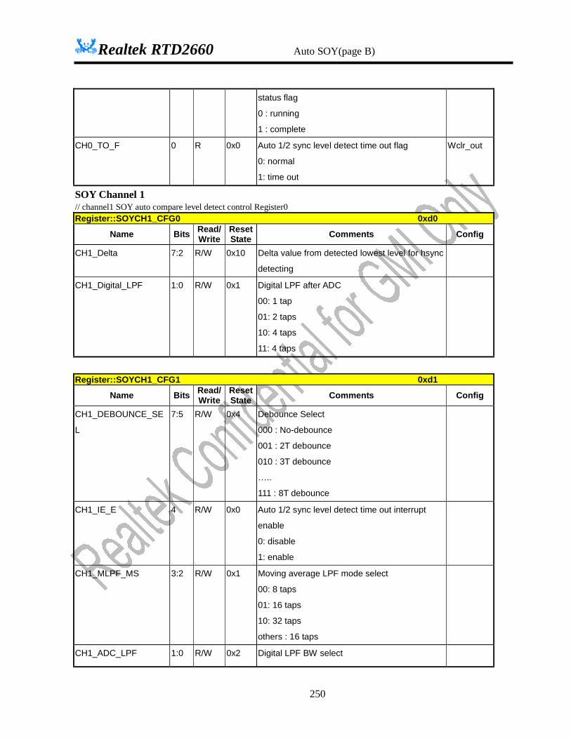
Realtek RTD2660 Auto SOY(page B)
250
status flag
0 : running
1 : complete
CH0_TO_F 0 R 0x0 Auto 1/2 sync level detect time out flag
0: normal
1: time out
Wclr_out
SOY Channel 1 // channel1 SOY auto compare level detect control Register0 Register::SOYCH1_CFG0 0xd0
Name Bits Read/Write
Reset State Comments Config
CH1_Delta 7:2 R/W 0x10 Delta value from detected lowest level for hsync
detecting
CH1_Digital_LPF 1:0 R/W 0x1 Digital LPF after ADC
00: 1 tap
01: 2 taps
10: 4 taps
11: 4 taps
Register::SOYCH1_CFG1 0xd1
Name Bits Read/Write
Reset State Comments Config
CH1_DEBOUNCE_SE
L
7:5 R/W 0x4 Debounce Select
000 : No-debounce
001 : 2T debounce
010 : 3T debounce
…..
111 : 8T debounce
CH1_IE_E 4 R/W 0x0 Auto 1/2 sync level detect time out interrupt
enable
0: disable
1: enable
CH1_MLPF_MS 3:2 R/W 0x1 Moving average LPF mode select
00: 8 taps
01: 16 taps
10: 32 taps
others : 16 taps
CH1_ADC_LPF 1:0 R/W 0x2 Digital LPF BW select

Realtek RTD2660 Auto SOY(page B)
251
00:2 points average filter
01:4 points average filter
10:8 points average filter
11:16 points average filter
default : 4 point average filter
// channel1 SOY auto compare level detect control Register1 Register::SOYCH1_CFG2 0xd2
Name Bits Read/Write
Reset State Comments Config
CH1_MODE 7 R/W 0x1 Auto 1/2 sync level detect mode
0: one shot
1: continue
CH1_OFFSET_V 6:0 R/W 0x0 offset value
SOY compare level=offset value+feedback
value
Bit 6 is sign bit
Register::SOYCH1_CFG3 0xd3
Name Bits Read/Write
Reset State Comments Config
CH1_ENABLE 7 R/W 0x0 Auto 1/2 sync level detect enable/ disable
0: disable
1: enable
Reserved 6 -
CH1_M_CMPL 5:0 R/W 0x1E Compare level Manual setting
Only valid when CH1_CMPL_U_Sel set 0
Register::SOYCH1_CFG4 0xd4
Name Bits Read/Write
Reset State Comments Config
CH1_D_TIME 7:4 R/W 0x4 Compare level auto update delay time after 1/2
sync level latched for continue mode.
The Dealy Time Output Hsync DC Level for
Analog Issue.
CH1_CMPL_U_Sel 3 R/W 0 Compare level update source sel
0: Manual compare level
1: Auto compare level
CH1_U_mode 2 R/W 0x0 Compare level update mode
0: normal

Realtek RTD2660 Auto SOY(page B)
252
1: step updating
CH1_U_step 1:0 R/W 0x0 compare level updating step
00:1/2 of sync DC_level(i)-DC_level(i-1)
01:1/4 of sync DC_level(i)-DC_level(i-1)
10:1/8 of sync DC_level(i)-DC_level(i-1)
11:1/16 of sync DC_level(i)-DC_level(i-1)
Register::SOYCH1_CFG5 0xd5
Name Bits Read/Write
Reset State Comments Config
Reserved 7:6 -
CH1_Min_diff 5:0 R/W 0x4 Minimum difference threshold to update
compare level
// channel1 SOY auto compare level detect control Register2 Register::SOYCH1_CFG6 0xd6
Name Bits Read/Write
Reset State Comments Config
CH1_TO_count_15_8 7:0 R/W 0x10 TO_count[15:8], Time Out counter for lowest
level to detect time out
Register::SOYCH1_CFG7 0xd7
Name Bits Read/Write
Reset State Comments Config
CH1_TO_count_7_0 7:0 R/W 0x00 TO_count[7:0], Time Out counter for lowest level
to detect time out
Register::SOYCH1_CFG8 0xd8
Name Bits Read/Write
Reset State Comments Config
CH1_L_count_15_8 7:0 R/W 0x08 L_count[15:8], Lowest level detect sample
count
Register::SOYCH1_CFG9 0xd9
Name Bits Read/Write
Reset State Comments Config
CH1_L_count_7_0 7:0 R/W 0x00 L_count[7:0], Lowest level detect sample count
// channel1 SOY auto compare level detect status Register0 Register::SOYCH1_CFGA 0xda

Realtek RTD2660 Auto SOY(page B)
253
Name Bits Read/Write
Reset State Comments Config
Reserved 7:6 -
CH1_A_CMPL 5:0 R 0x0 Current Compare level setting by auto detection
mechanism
Register::SOYCH1_CFGB 0xdb
Name Bits Read/Write
Reset State Comments Config
Reserved 7:6 -
CH1_OUT_DC 5:0 R 0x0 Value of detected DC level
Register::SOYCH1_CFGC 0xdc
Name Bits Read/Write
Reset State Comments Config
CH1_LOW_LEVEL 7:2 R 0x0 Detected Lowest level
CH1_OS_F 1 R 0x0 One shot mode Auto 1/2 sync level detection
status flag
0 : running
1 : complete
Wclr_out
CH1_TO_F 0 R 0x0 Auto 1/2 sync level detect time out flag
0: normal
1: time out
Wclr_out
Address:0xdf Reserved
SOY Channel 0 Calibration Ctrl Register:: SOYCH0_ Cali_CFG0 0xe0
Name Bits Read/Write
Reset State Comments Config
fporch_val_sel 7:4 R 5 Select the output value of ADC data, before the
rising edge of hsync. The base of fporch_val_sel is 4
clock cycle
Reserved 3 -
calibrate_cnt_base 2:0 R/W 4 Delay clock number to latch the output value of
ADC for ADC output stable issue.
Register:: SOYCH0_ Cali_CFG1 0xe1
Name Bits Read/Write
Reset State Comments Config
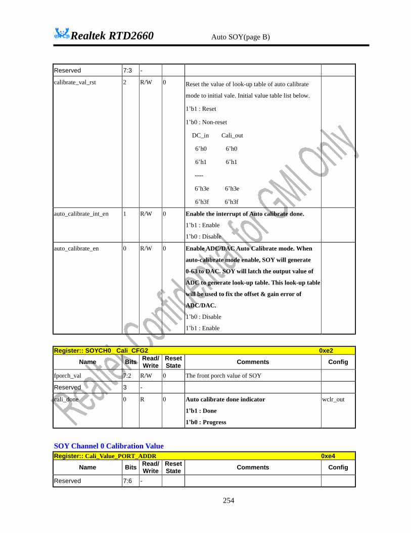
Realtek RTD2660 Auto SOY(page B)
254
Reserved 7:3 -
calibrate_val_rst 2 R/W 0 Reset the value of look-up table of auto calibrate
mode to initial vale. Initial value table list below.
1’b1 : Reset
1’b0 : Non-reset
DC_in Cali_out
6’h0 6’h0
6’h1 6’h1
----
6’h3e 6’h3e
6’h3f 6’h3f
auto_calibrate_int_en 1 R/W 0 Enable the interrupt of Auto calibrate done.
1’b1 : Enable
1’b0 : Disable
auto_calibrate_en 0 R/W 0 Enable ADC/DAC Auto Calibrate mode. When
auto-calibrate mode enable, SOY will generate
0-63 to DAC. SOY will latch the output value of
ADC to generate look-up table. This look-up table
will be used to fix the offset & gain error of
ADC/DAC.
1’b0 : Disable
1’b1 : Enable
Register:: SOYCH0_ Cali_CFG2 0xe2
Name Bits Read/Write
Reset State Comments Config
fporch_val 7:2 R/W 0 The front porch value of SOY
Reserved 3 -
cali_done 0 R 0 Auto calibrate done indicator
1’b1 : Done
1’b0 : Progress
wclr_out
SOY Channel 0 Calibration Value Register:: Cali_Value_PORT_ADDR 0xe4
Name Bits Read/Write
Reset State Comments Config
Reserved 7:6 -

Realtek RTD2660 Auto SOY(page B)
255
Cali_port_addr 5:0 R/W 0 Cali Value Access Port Address
Register:: Cali_Value_PORT_DATA 0xe5
Name Bits Read/Write
Reset State Comments Config
Cali_port_data 7:0 R/W 0x00 Cali Value Access Port Data
Register::Cali_Value_0 (ACCESS[E4,E5]) 0x00
Name Bits Read/Write
Reset State Comments Config
Reserved 7:6 -
cali_0 5:0 R 0 Auto Calibrate value of input 0 of ADC
Register:: Cali_Value_1 (ACCESS[E4,E5]) 0x01
Name Bits Read/Write
Reset State Comments Config
Reserved 7:6 -
cali_1 5:0 R 0 Auto Calibrate value of input 1 of ADC
Register:: Cali_Value_2 (ACCESS[E4,E5]) 0x02
Name Bits Read/Write
Reset State Comments Config
Reserved 7:6 -
cali_2 5:0 R 0 Auto Calibrate value of input 2 of ADC
Register:: Cali_Value_3 (ACCESS[E4,E5]) 0x03
Name Bits Read/Write
Reset State Comments Config
Reserved 7:6 -
cali_3 5:0 R 0 Auto Calibrate value of input 3 of ADC
Register:: Cali_Value_4 (ACCESS[E4,E5]) 0x04
Name Bits Read/Write
Reset State Comments Config
Reserved 7:6 -
cali_4 5:0 R 0 Auto Calibrate value of input 4 of ADC
Register:: Cali_Value_ 5 (ACCESS[E4,E5]) 0x05
Name Bits Read/Write
Reset State Comments Config
Reserved 7:6 -
cali_5 5:0 R 0 Auto Calibrate value of input 5 of ADC
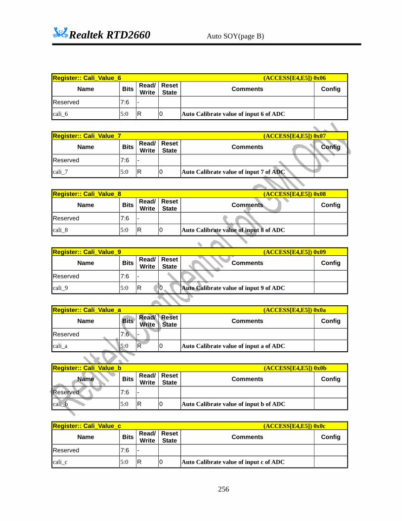
Realtek RTD2660 Auto SOY(page B)
256
Register:: Cali_Value_6 (ACCESS[E4,E5]) 0x06
Name Bits Read/Write
Reset State Comments Config
Reserved 7:6 -
cali_6 5:0 R 0 Auto Calibrate value of input 6 of ADC
Register:: Cali_Value_7 (ACCESS[E4,E5]) 0x07
Name Bits Read/Write
Reset State Comments Config
Reserved 7:6 -
cali_7 5:0 R 0 Auto Calibrate value of input 7 of ADC
Register:: Cali_Value_8 (ACCESS[E4,E5]) 0x08
Name Bits Read/Write
Reset State Comments Config
Reserved 7:6 -
cali_8 5:0 R 0 Auto Calibrate value of input 8 of ADC
Register:: Cali_Value_9 (ACCESS[E4,E5]) 0x09
Name Bits Read/Write
Reset State Comments Config
Reserved 7:6 -
cali_9 5:0 R 0 Auto Calibrate value of input 9 of ADC
Register:: Cali_Value_a (ACCESS[E4,E5]) 0x0a
Name Bits Read/Write
Reset State Comments Config
Reserved 7:6 -
cali_a 5:0 R 0 Auto Calibrate value of input a of ADC
Register:: Cali_Value_b (ACCESS[E4,E5]) 0x0b
Name Bits Read/Write
Reset State Comments Config
Reserved 7:6 -
cali_b 5:0 R 0 Auto Calibrate value of input b of ADC
Register:: Cali_Value_c (ACCESS[E4,E5]) 0x0c
Name Bits Read/Write
Reset State Comments Config
Reserved 7:6 -
cali_c 5:0 R 0 Auto Calibrate value of input c of ADC

Realtek RTD2660 Auto SOY(page B)
257
Register:: Cali_Value_d (ACCESS[E4,E5]) 0x0d
Name Bits Read/Write
Reset State Comments Config
Reserved 7:6 -
cali_d 5:0 R 0 Auto Calibrate value of input d of ADC
Register:: Cali_Value_e (ACCESS[E4,E5]) 0x0e
Name Bits Read/Write
Reset State Comments Config
Reserved 7:6 -
cali_e 5:0 R 0 Auto Calibrate value of input e of ADC
Register:: Cali_Value_f (ACCESS[E4,E5]) 0x0f
Name Bits Read/Write
Reset State Comments Config
Reserved 7:6 -
cali_f 5:0 R 0 Auto Calibrate value of input f of ADC
Register:: Cali_Value_10 (ACCESS[E4,E5]) 0x10
Name Bits Read/Write
Reset State Comments Config
Reserved 7:6 -
cali_10 5:0 R 0 Auto Calibrate value of input 10 of ADC
Register:: Cali_Value_11 (ACCESS[E4,E5]) 0x11
Name Bits Read/Write
Reset State Comments Config
Reserved 7:6 -
cali_11 5:0 R 0 Auto Calibrate value of input 11 of ADC
Register:: Cali_Value_12 (ACCESS[E4,E5]) 0x12
Name Bits Read/Write
Reset State Comments Config
Reserved 7:6 -
cali_12 5:0 R 0 Auto Calibrate value of input 12 of ADC
Register:: Cali_Value_13 (ACCESS[E4,E5]) 0x13
Name Bits Read/Write
Reset State Comments Config
Reserved 7:6 -
cali_13 5:0 R 0 Auto Calibrate value of input 13 of ADC

Realtek RTD2660 Auto SOY(page B)
258
Register:: Cali_Value_14 (ACCESS[E4,E5]) 0x14
Name Bits Read/Write
Reset State Comments Config
Reserved 7:6 -
cali_14 5:0 R 0 Auto Calibrate value of input 14 of ADC
Register:: Cali_Value_15 (ACCESS[E4,E5]) 0x15
Name Bits Read/Write
Reset State Comments Config
Reserved 7:6 -
cali_15 5:0 R 0 Auto Calibrate value of input 15 of ADC
Register:: Cali_Value_16 (ACCESS[E4,E5]) 0x16
Name Bits Read/Write
Reset State Comments Config
Reserved 7:6 -
cali_16 5:0 R 0 Auto Calibrate value of input 16 of ADC
Register:: Cali_Value_17 (ACCESS[E4,E5]) 0x17
Name Bits Read/Write
Reset State Comments Config
Reserved 7:6 -
cali_17 5:0 R 0 Auto Calibrate value of input 17 of ADC
Register:: Cali_Value_18 (ACCESS[E4,E5]) 0x18
Name Bits Read/Write
Reset State Comments Config
Reserved 7:6 -
cali_18 5:0 R 0 Auto Calibrate value of input 18 of ADC
Register:: Cali_Value_19 (ACCESS[E4,E5]) 0x19
Name Bits Read/Write
Reset State Comments Config
Reserved 7:6 -
cali_19 5:0 R 0 Auto Calibrate value of input 19 of ADC
Register:: Cali_Value_1a (ACCESS[E4,E5]) 0x1a
Name Bits Read/Write
Reset State Comments Config
Reserved 7:6 -
cali_1a 5:0 R 0 Auto Calibrate value of input 1a of ADC

Realtek RTD2660 Auto SOY(page B)
259
Register:: Cali_Value_1b (ACCESS[E4,E5]) 0x1b
Name Bits Read/Write
Reset State Comments Config
Reserved 7:6 -
cali_1b 5:0 R 0 Auto Calibrate value of input 1b of ADC
Register:: Cali_Value_1c (ACCESS[E4,E5]) 0x1c
Name Bits Read/Write
Reset State Comments Config
Reserved 7:6 -
cali_1c 5:0 R 0 Auto Calibrate value of input 1c of ADC
Register:: Cali_Value_1d (ACCESS[E4,E5]) 0x1d
Name Bits Read/Write
Reset State Comments Config
Reserved 7:6 -
cali_1d 5:0 R 0 Auto Calibrate value of input 1d of ADC
Register:: Cali_Value_1e (ACCESS[E4,E5]) 0x1e
Name Bits Read/Write
Reset State Comments Config
Reserved 7:6 -
cali_1e 5:0 R 0 Auto Calibrate value of input 1e of ADC
Register:: Cali_Value_1f (ACCESS[E4,E5]) 0x1f
Name Bits Read/Write
Reset State Comments Config
Reserved 7:6 -
cali_1f 5:0 R 0 Auto Calibrate value of input 1f of ADC
Register:: Cali_Value_20 (ACCESS[E4,E5]) 0x20
Name Bits Read/Write
Reset State Comments Config
Reserved 7:6 -
cali_20 5:0 R 0 Auto Calibrate value of input 20 of ADC
Register:: Cali_Value_21 (ACCESS[E4,E5]) 0x21
Name Bits Read/Write
Reset State Comments Config
Reserved 7:6 -
cali_21 5:0 R 0 Auto Calibrate value of input 21 of ADC
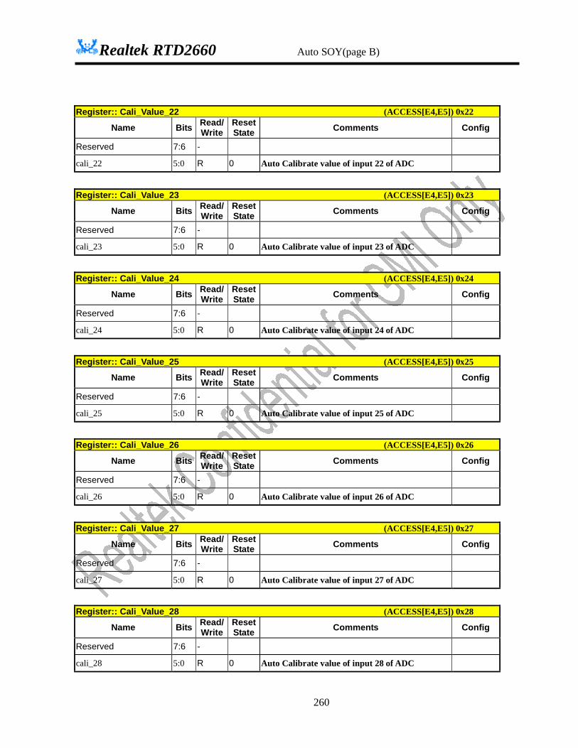
Realtek RTD2660 Auto SOY(page B)
260
Register:: Cali_Value_22 (ACCESS[E4,E5]) 0x22
Name Bits Read/Write
Reset State Comments Config
Reserved 7:6 -
cali_22 5:0 R 0 Auto Calibrate value of input 22 of ADC
Register:: Cali_Value_23 (ACCESS[E4,E5]) 0x23
Name Bits Read/Write
Reset State Comments Config
Reserved 7:6 -
cali_23 5:0 R 0 Auto Calibrate value of input 23 of ADC
Register:: Cali_Value_24 (ACCESS[E4,E5]) 0x24
Name Bits Read/Write
Reset State Comments Config
Reserved 7:6 -
cali_24 5:0 R 0 Auto Calibrate value of input 24 of ADC
Register:: Cali_Value_25 (ACCESS[E4,E5]) 0x25
Name Bits Read/Write
Reset State Comments Config
Reserved 7:6 -
cali_25 5:0 R 0 Auto Calibrate value of input 25 of ADC
Register:: Cali_Value_26 (ACCESS[E4,E5]) 0x26
Name Bits Read/Write
Reset State Comments Config
Reserved 7:6 -
cali_26 5:0 R 0 Auto Calibrate value of input 26 of ADC
Register:: Cali_Value_27 (ACCESS[E4,E5]) 0x27
Name Bits Read/Write
Reset State Comments Config
Reserved 7:6 -
cali_27 5:0 R 0 Auto Calibrate value of input 27 of ADC
Register:: Cali_Value_28 (ACCESS[E4,E5]) 0x28
Name Bits Read/Write
Reset State Comments Config
Reserved 7:6 -
cali_28 5:0 R 0 Auto Calibrate value of input 28 of ADC
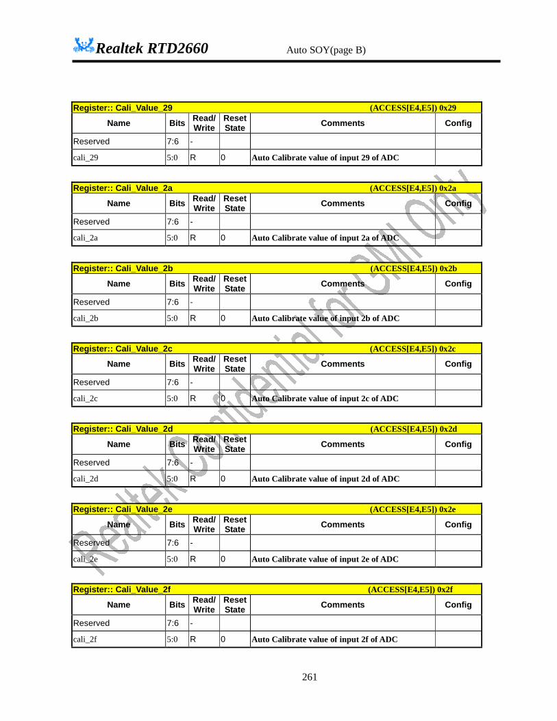
Realtek RTD2660 Auto SOY(page B)
261
Register:: Cali_Value_29 (ACCESS[E4,E5]) 0x29
Name Bits Read/Write
Reset State Comments Config
Reserved 7:6 -
cali_29 5:0 R 0 Auto Calibrate value of input 29 of ADC
Register:: Cali_Value_2a (ACCESS[E4,E5]) 0x2a
Name Bits Read/Write
Reset State Comments Config
Reserved 7:6 -
cali_2a 5:0 R 0 Auto Calibrate value of input 2a of ADC
Register:: Cali_Value_2b (ACCESS[E4,E5]) 0x2b
Name Bits Read/Write
Reset State Comments Config
Reserved 7:6 -
cali_2b 5:0 R 0 Auto Calibrate value of input 2b of ADC
Register:: Cali_Value_2c (ACCESS[E4,E5]) 0x2c
Name Bits Read/Write
Reset State Comments Config
Reserved 7:6 -
cali_2c 5:0 R 0 Auto Calibrate value of input 2c of ADC
Register:: Cali_Value_2d (ACCESS[E4,E5]) 0x2d
Name Bits Read/Write
Reset State Comments Config
Reserved 7:6 -
cali_2d 5:0 R 0 Auto Calibrate value of input 2d of ADC
Register:: Cali_Value_2e (ACCESS[E4,E5]) 0x2e
Name Bits Read/Write
Reset State Comments Config
Reserved 7:6 -
cali_2e 5:0 R 0 Auto Calibrate value of input 2e of ADC
Register:: Cali_Value_2f (ACCESS[E4,E5]) 0x2f
Name Bits Read/Write
Reset State Comments Config
Reserved 7:6 -
cali_2f 5:0 R 0 Auto Calibrate value of input 2f of ADC

Realtek RTD2660 Auto SOY(page B)
262
Register:: Cali_Value_30 (ACCESS[E4,E5]) 0x30
Name Bits Read/Write
Reset State Comments Config
Reserved 7:6 -
cali_30 5:0 R 0 Auto Calibrate value of input 30 of ADC
Register:: Cali_Value_31 (ACCESS[E4,E5]) 0x31
Name Bits Read/Write
Reset State Comments Config
Reserved 7:6 -
cali_31 5:0 R 0 Auto Calibrate value of input 31 of ADC
Register:: Cali_Value_32 (ACCESS[E4,E5]) 0x32
Name Bits Read/Write
Reset State Comments Config
Reserved 7:6 -
cali_32 5:0 R 0 Auto Calibrate value of input 32 of ADC
Register:: Cali_Value_33 (ACCESS[E4,E5]) 0x33
Name Bits Read/Write
Reset State Comments Config
Reserved 7:6 -
cali_33 5:0 R 0 Auto Calibrate value of input 33 of ADC
Register:: Cali_Value_34 (ACCESS[E4,E5]) 0x34
Name Bits Read/Write
Reset State Comments Config
Reserved 7:6 -
cali_34 5:0 R 0 Auto Calibrate value of input 34 of ADC
Register:: Cali_Value_35 (ACCESS[E4,E5]) 0x35
Name Bits Read/Write
Reset State Comments Config
Reserved 7:6 -
cali_35 5:0 R 0 Auto Calibrate value of input 35 of ADC
Register:: Cali_Value_36 (ACCESS[E4,E5]) 0x36
Name Bits Read/Write
Reset State Comments Config
Reserved 7:6 -
cali_36 5:0 R 0 Auto Calibrate value of input 36 of ADC

Realtek RTD2660 Auto SOY(page B)
263
Register:: Cali_Value_37 (ACCESS[E4,E5]) 0x37
Name Bits Read/Write
Reset State Comments Config
Reserved 7:6 -
cali_37 5:0 R 0 Auto Calibrate value of input 37 of ADC
Register:: Cali_Value_38 (ACCESS[E4,E5]) 0x38
Name Bits Read/Write
Reset State Comments Config
Reserved 7:6 -
cali_38 5:0 R 0 Auto Calibrate value of input 38 of ADC
Register:: Cali_Value_39 (ACCESS[E4,E5]) 0x39
Name Bits Read/Write
Reset State Comments Config
Reserved 7:6 -
cali_39 5:0 R 0 Auto Calibrate value of input 39 of ADC
Register:: Cali_Value_3a (ACCESS[E4,E5]) 0x3a
Name Bits Read/Write
Reset State Comments Config
Reserved 7:6 -
cali_3a 5:0 R 0 Auto Calibrate value of input 3a of ADC
Register:: Cali_Value_3b (ACCESS[E4,E5]) 0x3b
Name Bits Read/Write
Reset State Comments Config
Reserved 7:6 -
cali_3b 5:0 R 0 Auto Calibrate value of input 3b of ADC
Register:: Cali_Value_3c (ACCESS[E4,E5]) 0x3c
Name Bits Read/Write
Reset State Comments Config
Reserved 7:6 -
cali_3c 5:0 R 0 Auto Calibrate value of input 3c of ADC
Register:: Cali_Value_3d (ACCESS[E4,E5]) 0x3d
Name Bits Read/Write
Reset State Comments Config
Reserved 7:6 -
cali_3d 5:0 R 0 Auto Calibrate value of input 3d of ADC

Realtek RTD2660 Auto SOY(page B)
264
Register:: Cali_Value_3e (ACCESS[E4,E5]) 0x3e
Name Bits Read/Write
Reset State Comments Config
Reserved 7:6 -
cali_3e 5:0 R 0 Auto Calibrate value of input 3e of ADC
Register:: Cali_Value_3f (ACCESS[E4,E5]) 0x3f
Name Bits Read/Write
Reset State Comments Config
Reserved 7:6 -
cali_3f 5:0 R 0 Auto Calibrate value of input 3f of ADC

Realtek RTD2660 Auto SOY(page B)
265
SOY Channel 1 Calibration Ctrl Register:: SOYCH1_ Cali_CFG0 0xf0
Name Bits Read/Write
Reset State Comments Config
fporch_val_sel 7:4 R 5 Select the output value of ADC data, before the
rising edge of hsync. The base of fporch_val_sel is 4
clock cycle
Reserved 3 -
calibrate_cnt_base 2:0 R/W 4 Delay clock number to latch the output value of
ADC for ADC output stable issue.
Register:: SOYCH1_ Cali_CFG1 0xf1
Name Bits Read/Write
Reset State Comments Config
Reserved 7:3 -
calibrate_val_rst 2 R/W 0 Reset the value of look-up table of auto calibrate
mode to initial vale. Initial value table list below.
1’b1 : Reset
1’b0 : Non-reset
DC_in Cali_out
6’h0 6’h0
6’h1 6’h1
----
6’h3e 6’h3e
6’h3f 6’h3f
auto_calibrate_int_en 1 R/W 0 Enable the interrupt of Auto calibrate done.
1’b1 : Enable
1’b0 : Disable
auto_calibrate_en 0 R/W 0 Enable ADC/DAC Auto Calibrate mode. When
auto-calibrate mode enable, SOY will generate
0-63 to DAC. SOY will latch the output value of
ADC to generate look-up table. This look-up table
will be used to fix the offset & gain error of
ADC/DAC.
1’b0 : Disable
1’b1 : Enable

Realtek RTD2660 Auto SOY(page B)
266
Register:: SOYCH1_ Cali_CFG2 0xf2
Name Bits Read/Write
Reset State Comments Config
fporch_val 7:2 R/W 0 The front porch value of SOY
Reserved 3 -
cali_done 0 R 0 Auto calibrate done indicator
1’b1 : Done
1’b0 : Progress
wclr_out
SOY Channel 1 Calibration Value Register:: Cali_Value_PORT_ADDR 0xF4
Name Bits Read/Write
Reset State Comments Config
Reserved 7:6 -
Cali_port_addr 5:0 R/W 0 Cali Value Access Port Address
Register:: Cali_Value_PORT_DATA 0xF5
Name Bits Read/Write
Reset State Comments Config
Cali_port_data 7:0 R/W 0x00 Cali Value Access Port Data
Register::Cali_Value_0 (ACCESS[F4,F5]) 0x00
Name Bits Read/Write
Reset State Comments Config
Reserved 7:6 -
cali_0 5:0 R 0 Auto Calibrate value of input 0 of ADC
Register:: Cali_Value_1 (ACCESS[F4,F5]) 0x01
Name Bits Read/Write
Reset State Comments Config
Reserved 7:6 -
cali_1 5:0 R 0 Auto Calibrate value of input 1 of ADC
Register:: Cali_Value_2 (ACCESS[F4,F5]) 0x02
Name Bits Read/Write
Reset State Comments Config
Reserved 7:6 -
cali_2 5:0 R 0 Auto Calibrate value of input 2 of ADC
Register:: Cali_Value_3 (ACCESS[F4,F5]) 0x03
Name Bits Read/Write
Reset State Comments Config
Reserved 7:6 -

Realtek RTD2660 Auto SOY(page B)
267
cali_3 5:0 R 0 Auto Calibrate value of input 3 of ADC
Register:: Cali_Value_4 (ACCESS[F4,F5]) 0x04
Name Bits Read/Write
Reset State Comments Config
Reserved 7:6 -
cali_4 5:0 R 0 Auto Calibrate value of input 4 of ADC
Register:: Cali_Value_ 5 (ACCESS[F4,F5]) 0x05
Name Bits Read/Write
Reset State Comments Config
Reserved 7:6 -
cali_5 5:0 R 0 Auto Calibrate value of input 5 of ADC
Register:: Cali_Value_6 (ACCESS[F4,F5]) 0x06
Name Bits Read/Write
Reset State Comments Config
Reserved 7:6 -
cali_6 5:0 R 0 Auto Calibrate value of input 6 of ADC
Register:: Cali_Value_7 (ACCESS[F4,F5]) 0x07
Name Bits Read/Write
Reset State Comments Config
Reserved 7:6 -
cali_7 5:0 R 0 Auto Calibrate value of input 7 of ADC
Register:: Cali_Value_8 (ACCESS[F4,F5]) 0x08
Name Bits Read/Write
Reset State Comments Config
Reserved 7:6 -
cali_8 5:0 R 0 Auto Calibrate value of input 8 of ADC
Register:: Cali_Value_9 (ACCESS[F4,F5]) 0x09
Name Bits Read/Write
Reset State Comments Config
Reserved 7:6 -
cali_9 5:0 R 0 Auto Calibrate value of input 9 of ADC
Register:: Cali_Value_a (ACCESS[F4,F5]) 0x0a
Name Bits Read/Write
Reset State Comments Config
Reserved 7:6 -
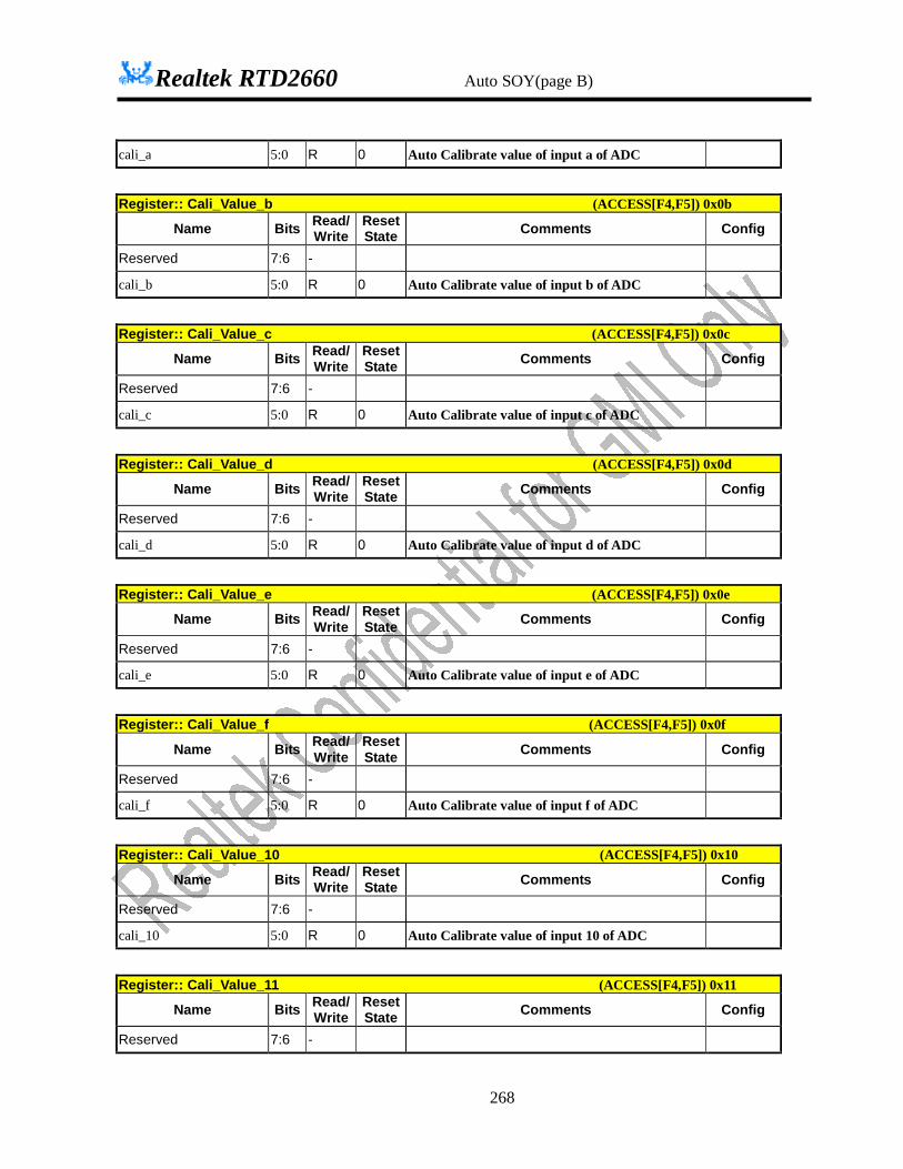
Realtek RTD2660 Auto SOY(page B)
268
cali_a 5:0 R 0 Auto Calibrate value of input a of ADC
Register:: Cali_Value_b (ACCESS[F4,F5]) 0x0b
Name Bits Read/Write
Reset State Comments Config
Reserved 7:6 -
cali_b 5:0 R 0 Auto Calibrate value of input b of ADC
Register:: Cali_Value_c (ACCESS[F4,F5]) 0x0c
Name Bits Read/Write
Reset State Comments Config
Reserved 7:6 -
cali_c 5:0 R 0 Auto Calibrate value of input c of ADC
Register:: Cali_Value_d (ACCESS[F4,F5]) 0x0d
Name Bits Read/Write
Reset State Comments Config
Reserved 7:6 -
cali_d 5:0 R 0 Auto Calibrate value of input d of ADC
Register:: Cali_Value_e (ACCESS[F4,F5]) 0x0e
Name Bits Read/Write
Reset State Comments Config
Reserved 7:6 -
cali_e 5:0 R 0 Auto Calibrate value of input e of ADC
Register:: Cali_Value_f (ACCESS[F4,F5]) 0x0f
Name Bits Read/Write
Reset State Comments Config
Reserved 7:6 -
cali_f 5:0 R 0 Auto Calibrate value of input f of ADC
Register:: Cali_Value_10 (ACCESS[F4,F5]) 0x10
Name Bits Read/Write
Reset State Comments Config
Reserved 7:6 -
cali_10 5:0 R 0 Auto Calibrate value of input 10 of ADC
Register:: Cali_Value_11 (ACCESS[F4,F5]) 0x11
Name Bits Read/Write
Reset State Comments Config
Reserved 7:6 -

Realtek RTD2660 Auto SOY(page B)
269
cali_11 5:0 R 0 Auto Calibrate value of input 11 of ADC
Register:: Cali_Value_12 (ACCESS[F4,F5]) 0x12
Name Bits Read/Write
Reset State Comments Config
Reserved 7:6 -
cali_12 5:0 R 0 Auto Calibrate value of input 12 of ADC
Register:: Cali_Value_13 (ACCESS[F4,F5]) 0x13
Name Bits Read/Write
Reset State Comments Config
Reserved 7:6 -
cali_13 5:0 R 0 Auto Calibrate value of input 13 of ADC
Register:: Cali_Value_14 (ACCESS[F4,F5]) 0x14
Name Bits Read/Write
Reset State Comments Config
Reserved 7:6 -
cali_14 5:0 R 0 Auto Calibrate value of input 14 of ADC
Register:: Cali_Value_15 (ACCESS[F4,F5]) 0x15
Name Bits Read/Write
Reset State Comments Config
Reserved 7:6 -
cali_15 5:0 R 0 Auto Calibrate value of input 15 of ADC
Register:: Cali_Value_16 (ACCESS[F4,F5]) 0x16
Name Bits Read/Write
Reset State Comments Config
Reserved 7:6 -
cali_16 5:0 R 0 Auto Calibrate value of input 16 of ADC
Register:: Cali_Value_17 (ACCESS[F4,F5]) 0x17
Name Bits Read/Write
Reset State Comments Config
Reserved 7:6 -
cali_17 5:0 R 0 Auto Calibrate value of input 17 of ADC
Register:: Cali_Value_18 (ACCESS[F4,F5]) 0x18
Name Bits Read/Write
Reset State Comments Config
Reserved 7:6 -

Realtek RTD2660 Auto SOY(page B)
270
cali_18 5:0 R 0 Auto Calibrate value of input 18 of ADC
Register:: Cali_Value_19 (ACCESS[F4,F5]) 0x19
Name Bits Read/Write
Reset State Comments Config
Reserved 7:6 -
cali_19 5:0 R 0 Auto Calibrate value of input 19 of ADC
Register:: Cali_Value_1a (ACCESS[F4,F5]) 0x1a
Name Bits Read/Write
Reset State Comments Config
Reserved 7:6 -
cali_1a 5:0 R 0 Auto Calibrate value of input 1a of ADC
Register:: Cali_Value_1b (ACCESS[F4,F5]) 0x1b
Name Bits Read/Write
Reset State Comments Config
Reserved 7:6 -
cali_1b 5:0 R 0 Auto Calibrate value of input 1b of ADC
Register:: Cali_Value_1c (ACCESS[F4,F5]) 0x1c
Name Bits Read/Write
Reset State Comments Config
Reserved 7:6 -
cali_1c 5:0 R 0 Auto Calibrate value of input 1c of ADC
Register:: Cali_Value_1d (ACCESS[F4,F5]) 0x1d
Name Bits Read/Write
Reset State Comments Config
Reserved 7:6 -
cali_1d 5:0 R 0 Auto Calibrate value of input 1d of ADC
Register:: Cali_Value_1e (ACCESS[F4,F5]) 0x1e
Name Bits Read/Write
Reset State Comments Config
Reserved 7:6 -
cali_1e 5:0 R 0 Auto Calibrate value of input 1e of ADC
Register:: Cali_Value_1f (ACCESS[F4,F5]) 0x1f
Name Bits Read/Write
Reset State Comments Config
Reserved 7:6 -

Realtek RTD2660 Auto SOY(page B)
271
cali_1f 5:0 R 0 Auto Calibrate value of input 1f of ADC
Register:: Cali_Value_20 (ACCESS[F4,F5]) 0x20
Name Bits Read/Write
Reset State Comments Config
Reserved 7:6 -
cali_20 5:0 R 0 Auto Calibrate value of input 20 of ADC
Register:: Cali_Value_21 (ACCESS[F4,F5]) 0x21
Name Bits Read/Write
Reset State Comments Config
Reserved 7:6 -
cali_21 5:0 R 0 Auto Calibrate value of input 21 of ADC
Register:: Cali_Value_22 (ACCESS[F4,F5]) 0x22
Name Bits Read/Write
Reset State Comments Config
Reserved 7:6 -
cali_22 5:0 R 0 Auto Calibrate value of input 22 of ADC
Register:: Cali_Value_23 (ACCESS[F4,F5]) 0x23
Name Bits Read/Write
Reset State Comments Config
Reserved 7:6 -
cali_23 5:0 R 0 Auto Calibrate value of input 23 of ADC
Register:: Cali_Value_24 (ACCESS[F4,F5]) 0x24
Name Bits Read/Write
Reset State Comments Config
Reserved 7:6 -
cali_24 5:0 R 0 Auto Calibrate value of input 24 of ADC
Register:: Cali_Value_25 (ACCESS[F4,F5]) 0x25
Name Bits Read/Write
Reset State Comments Config
Reserved 7:6 -
cali_25 5:0 R 0 Auto Calibrate value of input 25 of ADC
Register:: Cali_Value_26 (ACCESS[F4,F5]) 0x26
Name Bits Read/Write
Reset State Comments Config
Reserved 7:6 -

Realtek RTD2660 Auto SOY(page B)
272
cali_26 5:0 R 0 Auto Calibrate value of input 26 of ADC
Register:: Cali_Value_27 (ACCESS[F4,F5]) 0x27
Name Bits Read/Write
Reset State Comments Config
Reserved 7:6 -
cali_27 5:0 R 0 Auto Calibrate value of input 27 of ADC
Register:: Cali_Value_28 (ACCESS[F4,F5]) 0x28
Name Bits Read/Write
Reset State Comments Config
Reserved 7:6 -
cali_28 5:0 R 0 Auto Calibrate value of input 28 of ADC
Register:: Cali_Value_29 (ACCESS[F4,F5]) 0x29
Name Bits Read/Write
Reset State Comments Config
Reserved 7:6 -
cali_29 5:0 R 0 Auto Calibrate value of input 29 of ADC
Register:: Cali_Value_2a (ACCESS[F4,F5]) 0x2a
Name Bits Read/Write
Reset State Comments Config
Reserved 7:6 -
cali_2a 5:0 R 0 Auto Calibrate value of input 2a of ADC
Register:: Cali_Value_2b (ACCESS[F4,F5]) 0x2b
Name Bits Read/Write
Reset State Comments Config
Reserved 7:6 -
cali_2b 5:0 R 0 Auto Calibrate value of input 2b of ADC
Register:: Cali_Value_2c (ACCESS[F4,F5]) 0x2c
Name Bits Read/Write
Reset State Comments Config
Reserved 7:6 -
cali_2c 5:0 R 0 Auto Calibrate value of input 2c of ADC
Register:: Cali_Value_2d (ACCESS[F4,F5]) 0x2d
Name Bits Read/Write
Reset State Comments Config
Reserved 7:6 -

Realtek RTD2660 Auto SOY(page B)
273
cali_2d 5:0 R 0 Auto Calibrate value of input 2d of ADC
Register:: Cali_Value_2e (ACCESS[F4,F5]) 0x2e
Name Bits Read/Write
Reset State Comments Config
Reserved 7:6 -
cali_2e 5:0 R 0 Auto Calibrate value of input 2e of ADC
Register:: Cali_Value_2f (ACCESS[F4,F5]) 0x2f
Name Bits Read/Write
Reset State Comments Config
Reserved 7:6 -
cali_2f 5:0 R 0 Auto Calibrate value of input 2f of ADC
Register:: Cali_Value_30 (ACCESS[F4,F5]) 0x30
Name Bits Read/Write
Reset State Comments Config
Reserved 7:6 -
cali_30 5:0 R 0 Auto Calibrate value of input 30 of ADC
Register:: Cali_Value_31 (ACCESS[F4,F5]) 0x31
Name Bits Read/Write
Reset State Comments Config
Reserved 7:6 -
cali_31 5:0 R 0 Auto Calibrate value of input 31 of ADC
Register:: Cali_Value_32 (ACCESS[F4,F5]) 0x32
Name Bits Read/Write
Reset State Comments Config
Reserved 7:6 -
cali_32 5:0 R 0 Auto Calibrate value of input 32 of ADC
Register:: Cali_Value_33 (ACCESS[F4,F5]) 0x33
Name Bits Read/Write
Reset State Comments Config
Reserved 7:6 -
cali_33 5:0 R 0 Auto Calibrate value of input 33 of ADC
Register:: Cali_Value_34 (ACCESS[F4,F5]) 0x34
Name Bits Read/Write
Reset State Comments Config
Reserved 7:6 -

Realtek RTD2660 Auto SOY(page B)
274
cali_34 5:0 R 0 Auto Calibrate value of input 34 of ADC
Register:: Cali_Value_35 (ACCESS[F4,F5]) 0x35
Name Bits Read/Write
Reset State Comments Config
Reserved 7:6 -
cali_35 5:0 R 0 Auto Calibrate value of input 35 of ADC
Register:: Cali_Value_36 (ACCESS[F4,F5]) 0x36
Name Bits Read/Write
Reset State Comments Config
Reserved 7:6 -
cali_36 5:0 R 0 Auto Calibrate value of input 36 of ADC
Register:: Cali_Value_37 (ACCESS[F4,F5]) 0x37
Name Bits Read/Write
Reset State Comments Config
Reserved 7:6 -
cali_37 5:0 R 0 Auto Calibrate value of input 37 of ADC
Register:: Cali_Value_38 (ACCESS[F4,F5]) 0x38
Name Bits Read/Write
Reset State Comments Config
Reserved 7:6 -
cali_38 5:0 R 0 Auto Calibrate value of input 38 of ADC
Register:: Cali_Value_39 (ACCESS[F4,F5]) 0x39
Name Bits Read/Write
Reset State Comments Config
Reserved 7:6 -
cali_39 5:0 R 0 Auto Calibrate value of input 39 of ADC
Register:: Cali_Value_3a (ACCESS[F4,F5]) 0x3a
Name Bits Read/Write
Reset State Comments Config
Reserved 7:6 -
cali_3a 5:0 R 0 Auto Calibrate value of input 3a of ADC
Register:: Cali_Value_3b (ACCESS[F4,F5]) 0x3b
Name Bits Read/Write
Reset State Comments Config
Reserved 7:6 -

Realtek RTD2660 Auto SOY(page B)
275
cali_3b 5:0 R 0 Auto Calibrate value of input 3b of ADC
Register:: Cali_Value_3c (ACCESS[F4,F5]) 0x3c
Name Bits Read/Write
Reset State Comments Config
Reserved 7:6 -
cali_3c 5:0 R 0 Auto Calibrate value of input 3c of ADC
Register:: Cali_Value_3d (ACCESS[F4,F5]) 0x3d
Name Bits Read/Write
Reset State Comments Config
Reserved 7:6 -
cali_3d 5:0 R 0 Auto Calibrate value of input 3d of ADC
Register:: Cali_Value_3e (ACCESS[F4,F5]) 0x3e
Name Bits Read/Write
Reset State Comments Config
Reserved 7:6 -
cali_3e 5:0 R 0 Auto Calibrate value of input 3e of ADC
Register:: Cali_Value_3f (ACCESS[F4,F5]) 0x3f
Name Bits Read/Write
Reset State Comments Config
Reserved 7:6 -
cali_3f 5:0 R 0 Auto Calibrate value of input 3f of ADC

Realtek RTD2660 MCU register 1(page D)
276
Reserved page MCU register 1(page D) Embedded MCU Function
Designware DW8051 of Synopsys is integrated into this chip and is compatible with other industry 8051 series. A lot of peripherals are integrated and accessed by XFR (eXternal Function Register). When embedded MCU is used, scalar-related registers are access via XFR, too. The program code is stored in external serial FLASH. If the external MCU is used, the integrated peripherals can be accessed via special page in scalar’s register map.
Features l 8051 core, CPU operating frequency up to 50MHz l 256-byte IRAM, 256~1024 byte shared XRAM l external serial FLASH, support GPIO bank switching for 128K byte and up to 16M bytes
for XFR bank switching l Compliant with VESA DDC1/2B/2Bi/CI l Embedded triple ports DDC RAM(0~768 bytes shared with X-RAM) l Six channels of PWM DAC l Watchdog timer with programmable interval l Three 16-bit counters/timers (T0, T1, and ET2) l Programmable frequency clock output, 2 clock output ports l One full-duplex serial port l Six interrupt sources with 2 external interrupts l Five channels of 6-bit ADC, Three channels of 10-bit ADC l Hardware ISP, no boot code required l Built-in Low voltage reset circuit

Realtek RTD2660 MCU register 1(page D)
277
PWM generatorPWM
generatorPWM X 6
0x00 - 0xFFInternal RAM
256 bytes
IRAM_bus
DW8051_core
ISP MuxSPI FLASH Controller
Watch dog
InterruptController
CLK GEN
ExternalTimer clock
gen.
Timer 0
Timer 1
Timer 2
MCU/FLASH architecture for MFM
Serial port 0
CLKO1, CLKO2
Host Interface
0xFF00 -0xFFFF
XFR
8 bit ADCANA
ADC TDM
XRAM Arbitor
External Memory Space
Burst Read
DDC-CI
SFR Control Port
SFR_bus
LVR&Reset Control
Watch Dog Timter
ISP mode
DDC R/W
XFR in ISP
Program/XData
DDC slaveX3
0xFE00 -0xFE7FDDC1_RAM 128 byte
0xFD80 - 0xFDFFDDC0_RAM 128 byte
0xFB00 - 0xFD7FExternal RAM 640 byte
0xFE80 -0xFEFFDDC2_RAM 128 byte
IrDA
DDC Master
Internal Scalar Reg Inf
10 bit ADCANA
External Scalar Reg Inf
UART
PLL input
DW8051 micro-processor
The DW8051 is compatible with industry standard 803x/805x and provides the following
design features and enhancements to the standard 8051 microcontroller: High speed architecture
Compared to standard 8051, the DW8051 processor core provides increased performance by executing instructions in a 4-clock bus cycle, as opposed to the

Realtek RTD2660 MCU register 1(page D)
278
12-clock bus cycle in the standard 8051. The shortened bus timing improves the instruction execution rate for most instructions by a factor of three over the standard 8051 architectures. The average speed improvement for the entire instruction set is approximately 2.5X. Stretch Memory Cycles
The stretch memory cycle feature enables application software to adjust the speed of data memory access. The DW8051 can execute the MOVX instruction in as little as 2 instruction cycles. However, it is sometimes desirable to stretch this value; for example, to access slow memory or slow memory-mapped peripherals such as UARTs or LCDs.
The three LSBs of the Clock Control Register (at SFR location 8Eh) control the stretch value. You can use stretch values between zero and seven. A stretch value of zero adds zero instruction cycles, resulting in MOVX instructions executing in two instruction cycles. A stretch value of seven adds seven instruction cycles, resulting in MOVX instructions executing in nine instruction cycles. The stretch value can be changed dynamically under program control.
By default, the stretch value resets to one (three cycle MOVX). For full-speed data memory access, the software must set the stretch value to zero. The stretch value affects only data memory access. The only way to reduce the speed of program memory (ROM) access is to use a slower clock. Dual Data Pointers
The DW8051 employs dual data pointers to accelerate data memory block moves. The standard 8051 data pointer (DPTR) is a 16-bit value used to address external data RAM or peripherals. The DW8051 maintains the standard data pointer as DPTR0 at SFR locations 82h and 83h. It is not necessary to modify code to use DPTR0.
The DW8051 adds a second data pointer (DPTR1) at SFR locations 84h and 85h. The SEL bit in the DPTR Select register, DPS (SFR 86h), selects the active pointer. When SEL = 0, instructions that use the DPTR will use DPL0 and DPH0. When SEL = 1, instructions that use the DPTR will use DPL1 and DPH1. SEL is the bit 0 of SFR location 86h. No other bits of SFR location 86h are used.
All DPTR-related instructions use the currently selected data pointer. To switch the active pointer, toggle the SEL bit. The fastest way to do so is to use the increment instruction (INC DPS). This requires only one instruction to switch from a source address to a destination address, saving application code from having to save source and destination addresses when doing a block move.
Using dual data pointers provides significantly increased efficiency when moving large blocks of data.

Realtek RTD2660 MCU register 1(page D)
279
Timer Rate Control One important difference exists between the DW8051 and 80C32 regarding timers. The
original 80C32 used a 12 clock per cycle scheme for timers and consequently for some serial baud rates(depending on the mode). The DW8051 architecture normally runs using 4 clocks per cycle. However, in the area of timers, it will default to a 12 clock per cycle scheme on a reset. This allows existing code with real–time dependencies such as baud rates to operate properly. If an application needs higher speed timers or serial baud rates, the timers can be set to run at the 4 clock rate. The Clock Control register (CKCON – 8Eh) determines these timer speeds. When the relevant CKCON bit is a logic 1, the device uses 4 clocks per cycle to generate timer speeds. When the control bit is set to a zero, the device uses 12 clocks for timer speeds. The reset condition is a 0. CKCON.5 selects the speed of Timer 2. CKCON.4 selects Timer 1 and CKCON.3 selects Timer zero. Note that unless a user desires very fast timing, it is unnecessary to alter these bits. Note that the timer controls are independent. RESET
There are five reset sources.
l RST pin The external reset is high active and its pulse width must be larger than 8 clock cycles. The RST pin can reset the DW8051
l Low voltage reset(LVR) and power on reset(POR) l Software can use SOF_RST register to reset whole chip l Watchdog can reset DW8051 l When entering ISP mode, DW8051 will in reset state. When exiting ISP mode, DW8051 will
also asserting a reset, too.
Special Function Registers
Register Bit 7 Bit 6 Bit 5 Bit 4 Bit 3 Bit 2 Bit 1 Bit 0 Addr SP 81h DPL0 82h DPH0 83h DPL1 84h DPH1 85h DPS 0 0 0 0 0 0 0 SEL 86h

Realtek RTD2660 MCU register 1(page D)
280
PCON SMOD 0
1 1 GF1 GF0 STOP IDLE 87h
TCON TF1 TR1 TF0 TR0 IE1 IT1 IE0 IT0 88h TMOD GATE C/T M1 M0 GATE C/T M1 M0 89h TL0 8Ah TL1 8Bh TH0 8Ch TH1 8Dh CKCON T2M T1M T0M MD2 MD1 MD0 8Eh SPC_FNC 0 0 0 0 0 0 0 WRS 8Fh P1 P1.7 P1.6 P1.5 P1.4 P1.3 P1.2 P1.1 P1.0 90h MPAGE 92h SCON0 SM0 SM1 SM2 REN TB8 RB8 TI RI 98h SBUF0 99h P2 P2.7 P2.6 P2.5 P2.4 P2.3 P2.2 P2.1 P2.0 A0h IE EA 0 ET2 ES0 ET1 EX1 ET0 EX0 A8h P3 P3.7 P3.6 P3.5 P3.4 P3.3 P3.2 P3.1 P3.0 B0h IP 1 0 PT2 PS0 PT1 PX1 PT0 PX0 B8h T2CON TF2 EXF2 RCLK TCLK EXEN2 TR2 C/T2 CP/
RL2 C8h
RCAP2L CAh RCAP2H CBh TL2 CCh TH2 CDh PSW CY AC F0 RS1 RS0 OV F1 P D0h ACC E0h B F0h
Note: WRS of SPC_FNC register is tied zero. MPAGE is not used if we implement P2. 藍色部分
為DW8051有的而 standard 8051沒有的.紅色部分為DW8051沒有的而 standard 8051有,但也用
不到,所以 final spec 也不會列出. 橘色部分為DW8051沒有而我們必須 implement 的部分. SFR reset value
Register Bit 7 Bit 6 Bit 5 Bit 4 Bit 3 Bit 2 Bit 1 Bit 0 Addr SP 0 0 0 0 0 1 1 1 81h

Realtek RTD2660 MCU register 1(page D)
281
DPL0 0 0 0 0 0 0 0 0 82h DPH0 0 0 0 0 0 0 0 0 83h DPL1 0 0 0 0 0 0 0 0 84h DPH1 0 0 0 0 0 0 0 0 85h DPS 0 0 0 0 0 0 0 0 86h PCON 0 0 1 1 0 0 0 0 87h TCON 0 0 0 0 0 0 0 0 88h TMOD 0 0 0 0 0 0 0 0 89h TL0 0 0 0 0 0 0 0 0 8Ah TL1 0 0 0 0 0 0 0 0 8Bh TH0 0 0 0 0 0 0 0 0 8Ch TH1 0 0 0 0 0 0 0 0 8Dh CKCON 0 0 0 0 0 0 0 1 8Eh SPC_FNC 0 0 0 0 0 0 0 0 8Fh P1_W 1 1 1 1 1 1 1 1 90h MPAGE 0 0 0 0 0 0 0 0 92h P1_R 1 1 1 1 1 1 1 1 93h SCON0 0 0 0 0 0 0 0 0 98h SBUF0 0 0 0 0 0 0 0 0 99h P2 0 0 0 0 0 0 0 0 A0h IE 0 0 0 0 0 0 0 0 A8h P3_W 1 1 1 1 1 1 1 1 B0h P3_R 1 1 1 1 1 1 1 1 B3h IP 1 0 0 0 0 0 0 0 B8h T2CON 0 0 0 0 0 0 0 0 C8h RCAP2L 0 0 0 0 0 0 0 0 CAh RCAP2H 0 0 0 0 0 0 0 0 CBh TL2 0 0 0 0 0 0 0 0 CCh TH2 0 0 0 0 0 0 0 0 CDh PSW 0 0 0 0 0 0 0 0 D0h ACC 0 0 0 0 0 0 0 0 E0h B 0 0 0 0 0 0 0 0 F0h
DW8051 user-modifiable parameters ram_256 1

Realtek RTD2660 MCU register 1(page D)
282
timer2 1 rom_addr_size 0 Serial 1 extd_intr 0
REG_XFR_WRAPPER is the eXternal Function Register defined in 0xFF00 ~ 0xFFFF in DW8051’s XDATA memory space. There are three possible input sources for REG_XFR_WRAPPER. In embedded MCU mode, DW8051 has the power of control. PAGE D PAGE E PAGE F
A B C D E F A B C D E F A B C D
0xFFXX 0 1 2 3 4 5 6 7 8 9 A B C D E F
0 GPIO
1
2
SFR, P1
3 P3
4
5
6
Pin share
7
8
9
A 0x36
B CEC
C 0x37
D 0x38
E 0x39
F 0x40
In external MCU mode, external host interface has the privilege to access
REG_XFR_WRAPPER. The total 256 addresses are separated into 3 pages. 0xFF00 ~ 0xFF5F is Page D, 0xFF60 ~0xFFBF is Page E and 0xFFC0 ~ 0xFFFF is Page F. External host control signals are passed to scalar register interface. Host interface must integrate the output of scalar interface and REG_XFR_WRAPPER depends on page selection.

Realtek RTD2660 MCU register 1(page D)
283
When ISP is activated, REG_XFR_WRAPPER is accessed by ISP interface, it has the highest priority. DW8051 and external host is selected by power-on-latch signal, ext_host_sel.
Interrupt Control
Register::IRQ_Status 0xFF00
Name Bits R/W Default Comments Config
Reserved 7 -- -- Reserved
M2PLL_IRQ_EVENT 6 R/W 0 M2PLL-abnormal Event Status 1. Select M2PLL as clock source, but M2PLL power
down, power saving or output disable, clear this bit to
disable the interrupt
Rport Wport
CEC_IRQ_EVENT 5 R/W 0 CEC Event Status
1. IF CEC func IRQ event occurred since the last status
cleared
Rport Wport
SCA_IRQ_EVENT 4 R/W 0 Scalar-related Event Status
1. IF Scalar integrated IRQ event occurred since the last
status cleared
Rport Wport
I2CM_IRQ_EVENT 3 R/W 0 I2C Master Event Status
1. IF I2C Master IRQ event occurred since the last
status cleared
Rport Wport
ADC_IRQ_EVENT 2 R/W 0 ADC Event Status
1: If the ADC IRQ event occurred since the last status
cleared
Rport Wport
IrDA_IRQ_EVENT 1 R/W 0 IrDA Event Status
1: If the IrDA IRQ event occurred since the last status
cleared
Rport Wport
DDC_IRQ_EVENT 0 R/W 0 DDC Event Status
1: If the DDC IRQ event occurred since the last status
cleared
Rport Wport
Register::IRQ_Priority 0xFF01
Name Bits R/W Default Comments Config
Reserved 7 -- -- Reserved

Realtek RTD2660 MCU register 1(page D)
284
M2PLL_IRQ_PRI 6 R/W 0 M2PLL-abnormal IRQ Priority 0: Connected to int0
1: Connected to int1
CEC_IRQ_PRI 5 R/W 0 CEC IRQ Priority
0: Connected to int0
1: Connected to int1
SCA_IRQ_PRI 4 R/W 0 Scalar integrated IRQ Priority
0: Connected to int0
1: Connected to int1
I2CM_IRQ_PRI 3 R/W 0 I2C Master IRQ Priority
0: Connected to int0
1: Connected to int1
ADC_IRQ_PRI 2 R/W 0 ADC IRQ Priority
0: Connected to int0
1: Connected to int1
IrDA_IRQ_PRI 1 R/W 0 IrDA IRQ Priority
0: Connected to int0
1: Connected to int1
DDC_IRQ_PRI 0 R/W 0 DDC IRQ Priority
0: Connected to int0
1: Connected to int1
Register:: REV_DUMMY1 0xFF02
Name Bits R/W Default Comments Config
REV_DUMMY1 7:0 R/W 00 Dummy1
ADC
A/D Converter
RTD2662 has embedded 5 channels of analog-to-digital converter by A_circuit. The ADCs_ACKT convert analog input voltage on the five A/D input pins to five 6-bit digital data stored in XFRs (FF09 ~ FF0D) sequentially. The ADC conversion range is from GND to VDD and the conversion is linear and monotonic with no missing codes. To start A/D conversion, set STRT_ADC_ACKT = 1 and the conversion will be
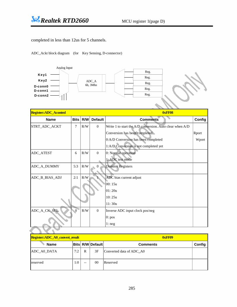
Realtek RTD2660 MCU register 1(page D)
285
completed in less than 12us for 5 channels. ADC_Ackt block diagram (for Key Sensing, D-connector)
ADC_A6b, 3Mhz
Reg.Key1
Analog Input
Key2
D-conn0D-conn1D-conn2
Reg.
Reg.
Reg.
Reg.
Register::ADC_Acontrol 0xFF08
Name Bits R/W Default Comments Config
STRT_ADC_ACKT 7 R/W 0 Write 1 to start the A/D conversion. Auto clear when A/D
Conversion has been completed.
0:A/D Conversion has been completed
1:A/D Conversion is not completed yet
Rport
Wport
ADC_ATEST 6 R/W 0 0: Normal operation
1: ADC test mode
ADC_A_DUMMY 5:3 R/W 0 Dummy Registers
ADC_B_BIAS_ADJ 2:1 R/W 1 ADC bias current adjust
00: 15u
01: 20u
10: 25u
11: 30u
ADC_A_CK_SEL 0 R/W 0 Inverse ADC input clock pos/neg
0: pos
1: neg
Register::ADC_A0_convert_result 0xFF09
Name Bits R/W Default Comments Config
ADC_A0_DATA 7:2 R 3F Converted data of ADC_A0
reserved 1:0 -- 00 Reserved
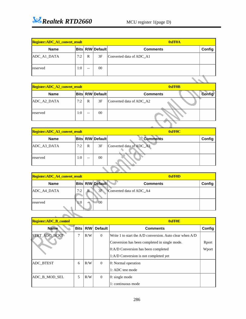
Realtek RTD2660 MCU register 1(page D)
286
Register::ADC_A1_convert_result 0xFF0A
Name Bits R/W Default Comments Config
ADC_A1_DATA 7:2 R 3F Converted data of ADC_A1
reserved 1:0 -- 00
Register::ADC_A2_convert_result 0xFF0B
Name Bits R/W Default Comments Config
ADC_A2_DATA 7:2 R 3F Converted data of ADC_A2
reserved 1:0 -- 00
Register::ADC_A3_convert_result 0xFF0C
Name Bits R/W Default Comments Config
ADC_A3_DATA 7:2 R 3F Converted data of ADC_A3
reserved 1:0 -- 00
Register::ADC_A4_convert_result 0xFF0D
Name Bits R/W Default Comments Config
ADC_A4_DATA 7:2 R 3F Converted data of ADC_A4
reserved 1:0 -- 00
Register::ADC_B_control 0xFF0E
Name Bits R/W Default Comments Config
STRT_ADC_BCKT 7 R/W 0 Write 1 to start the A/D conversion. Auto clear when A/D
Conversion has been completed in single mode.
0:A/D Conversion has been completed
1:A/D Conversion is not completed yet
Rport
Wport
ADC_BTEST 6 R/W 0 0: Normal operation
1: ADC test mode
ADC_B_MOD_SEL 5 R/W 0 0: single mode
1: continuous mode
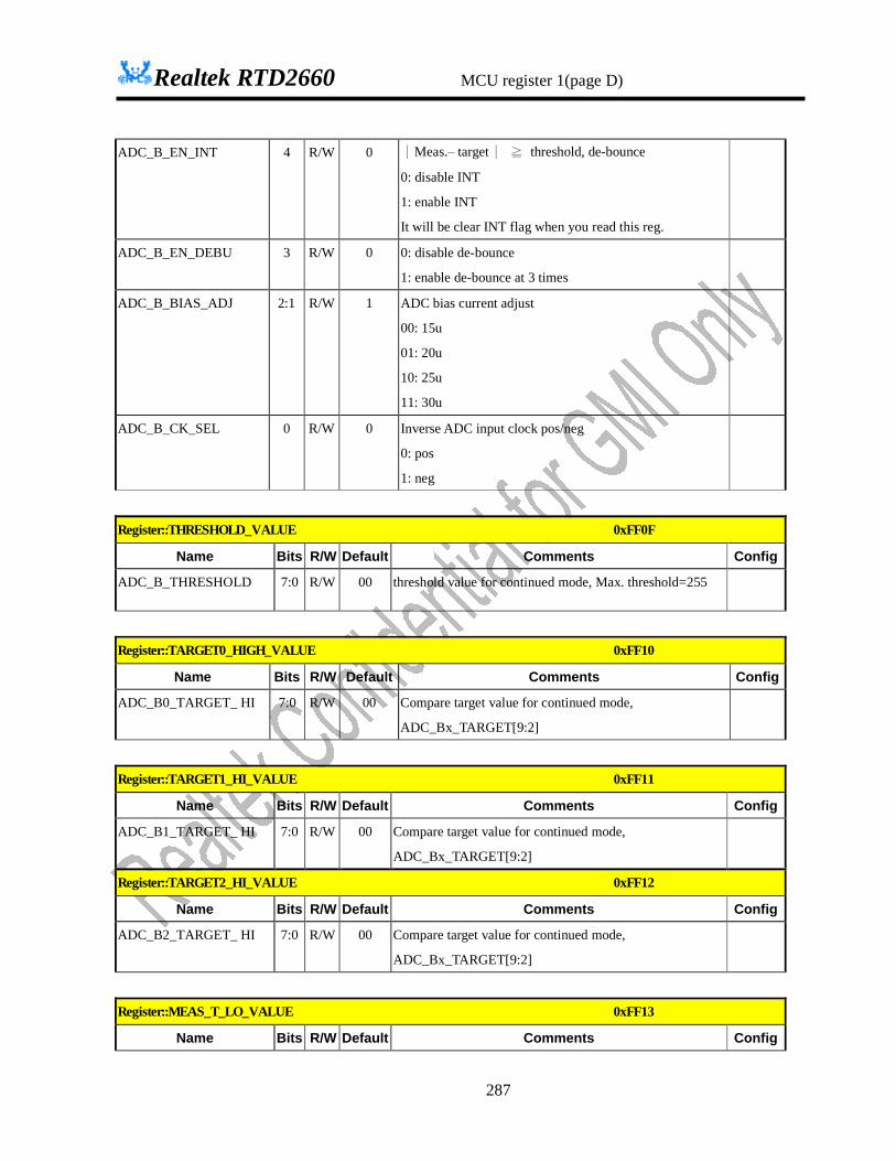
Realtek RTD2660 MCU register 1(page D)
287
ADC_B_EN_INT 4 R/W 0 ∣Meas.– target∣ ≧ threshold, de-bounce
0: disable INT
1: enable INT
It will be clear INT flag when you read this reg.
ADC_B_EN_DEBU 3 R/W 0 0: disable de-bounce
1: enable de-bounce at 3 times
ADC_B_BIAS_ADJ 2:1 R/W 1 ADC bias current adjust
00: 15u
01: 20u
10: 25u
11: 30u
ADC_B_CK_SEL 0 R/W 0 Inverse ADC input clock pos/neg
0: pos
1: neg
Register::THRESHOLD_VALUE 0xFF0F
Name Bits R/W Default Comments Config
ADC_B_THRESHOLD 7:0 R/W 00 threshold value for continued mode, Max. threshold=255
Register::TARGET0_HIGH_VALUE 0xFF10
Name Bits R/W Default Comments Config
ADC_B0_TARGET_ HI 7:0 R/W 00 Compare target value for continued mode,
ADC_Bx_TARGET[9:2]
Register::TARGET1_HI_VALUE 0xFF11
Name Bits R/W Default Comments Config
ADC_B1_TARGET_ HI 7:0 R/W 00 Compare target value for continued mode,
ADC_Bx_TARGET[9:2]
Register::TARGET2_HI_VALUE 0xFF12
Name Bits R/W Default Comments Config
ADC_B2_TARGET_ HI 7:0 R/W 00 Compare target value for continued mode,
ADC_Bx_TARGET[9:2]
Register::MEAS_T_LO_VALUE 0xFF13
Name Bits R/W Default Comments Config
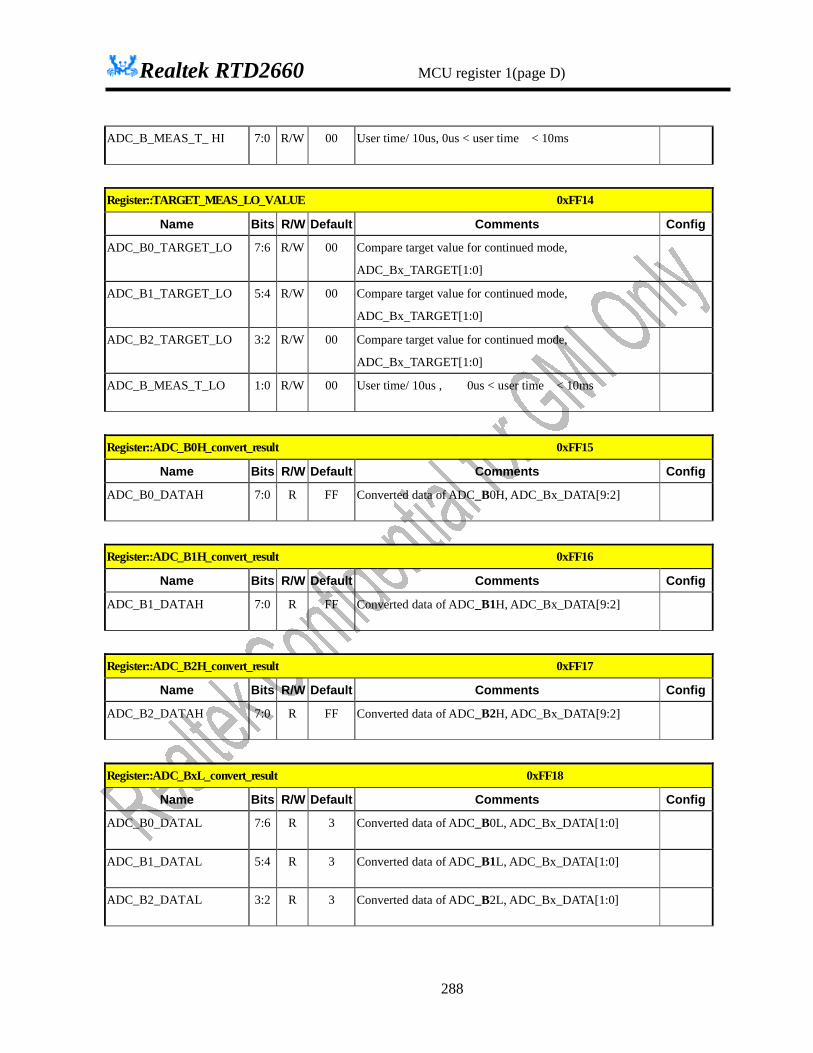
Realtek RTD2660 MCU register 1(page D)
288
ADC_B_MEAS_T_ HI 7:0 R/W 00 User time/ 10us, 0us < user time < 10ms
Register::TARGET_MEAS_LO_VALUE 0xFF14
Name Bits R/W Default Comments Config
ADC_B0_TARGET_LO 7:6 R/W 00 Compare target value for continued mode,
ADC_Bx_TARGET[1:0]
ADC_B1_TARGET_LO 5:4 R/W 00 Compare target value for continued mode,
ADC_Bx_TARGET[1:0]
ADC_B2_TARGET_LO 3:2 R/W 00 Compare target value for continued mode,
ADC_Bx_TARGET[1:0]
ADC_B_MEAS_T_LO 1:0 R/W 00 User time/ 10us , 0us < user time < 10ms
Register::ADC_B0H_convert_result 0xFF15
Name Bits R/W Default Comments Config
ADC_B0_DATAH 7:0 R FF Converted data of ADC_B0H, ADC_Bx_DATA[9:2]
Register::ADC_B1H_convert_result 0xFF16
Name Bits R/W Default Comments Config
ADC_B1_DATAH 7:0 R FF Converted data of ADC_B1H, ADC_Bx_DATA[9:2]
Register::ADC_B2H_convert_result 0xFF17
Name Bits R/W Default Comments Config
ADC_B2_DATAH 7:0 R FF Converted data of ADC_B2H, ADC_Bx_DATA[9:2]
Register::ADC_BxL_convert_result 0xFF18
Name Bits R/W Default Comments Config
ADC_B0_DATAL 7:6 R 3 Converted data of ADC_B0L, ADC_Bx_DATA[1:0]
ADC_B1_DATAL 5:4 R 3 Converted data of ADC_B1L, ADC_Bx_DATA[1:0]
ADC_B2_DATAL 3:2 R 3 Converted data of ADC_B2L, ADC_Bx_DATA[1:0]
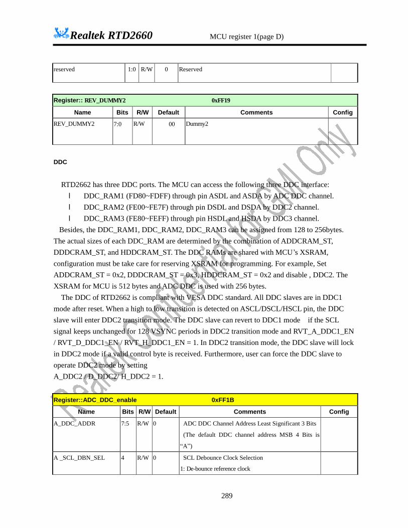
Realtek RTD2660 MCU register 1(page D)
289
reserved 1:0 R/W 0 Reserved
Register:: REV_DUMMY2 0xFF19
Name Bits R/W Default Comments Config
REV_DUMMY2 7:0 R/W 00 Dummy2
DDC
RTD2662 has three DDC ports. The MCU can access the following three DDC interface: l DDC_RAM1 (FD80~FDFF) through pin ASDL and ASDA by ADC DDC channel. l DDC_RAM2 (FE00~FE7F) through pin DSDL and DSDA by DDC2 channel. l DDC_RAM3 (FE80~FEFF) through pin HSDL and HSDA by DDC3 channel.
Besides, the DDC_RAM1, DDC_RAM2, DDC_RAM3 can be assigned from 128 to 256bytes. The actual sizes of each DDC_RAM are determined by the combination of ADDCRAM_ST, DDDCRAM_ST, and HDDCRAM_ST. The DDC RAMs are shared with MCU’s XSRAM, configuration must be take care for reserving XSRAM for programming. For example, Set ADDCRAM_ST = 0x2, DDDCRAM_ST = 0x3, HDDCRAM_ST = 0x2 and disable , DDC2. The XSRAM for MCU is 512 bytes and ADC DDC is used with 256 bytes.
The DDC of RTD2662 is compliant with VESA DDC standard. All DDC slaves are in DDC1 mode after reset. When a high to low transition is detected on ASCL/DSCL/HSCL pin, the DDC slave will enter DDC2 transition mode. The DDC slave can revert to DDC1 mode if the SCL signal keeps unchanged for 128 VSYNC periods in DDC2 transition mode and RVT_A_DDC1_EN / RVT_D_DDC1_EN / RVT_H_DDC1_EN = 1. In DDC2 transition mode, the DDC slave will lock in DDC2 mode if a valid control byte is received. Furthermore, user can force the DDC slave to operate DDC2 mode by setting A_DDC2 / D_DDC2/ H_DDC2 = 1. Register::ADC_DDC_enable 0xFF1B
Name Bits R/W Default Comments Config
A_DDC_ADDR 7:5 R/W 0 ADC DDC Channel Address Least Significant 3 Bits
(The default DDC channel address MSB 4 Bits is
“A”)
A _SCL_DBN_SEL 4 R/W 0 SCL Debounce Clock Selection
1: De-bounce reference clock

Realtek RTD2660 MCU register 1(page D)
290
0: De-bounce clock (after clock divider)
A_DDC_W_STA 3 R/W 0 ADC DDC Write Status (for external DDC access
only)
It is cleared after write. (No matter what the data are)
Rport
wport
A_DDCRAM_W_EN 2 R/W 0 ADC DDC SRAM Write Enable (for external DDC
access only)
0: Disable
1: Enable
A_DBN_EN 1 R/W 1 ADC DDC De-bounce Enable
0: Disable
1: Enable (with crystal/4)
A_DDC_EN 0 R/W 0 ADC DDC Channel Enable Bit
0: MCU access Enable
1: DDC channel Enable
Register::ADC_DDC_control_1 0xFF1C
Name Bits R/W Default Comments Config
A_DBN_CLK_SEL 7:6 R/W 0 De-bounce clock divider
00: 1/1 reference clock
01: 1/2 reference clock
1X: 1/4 reference clock
A_STOP_DBN_SEL 5:4 R/W 0 De-bounce sda stage
0X: latch one stage
10: latch two stage
11: latch three stage
A_SYS_CK_SEL 3 R/W 0 De-bounce reference clock
0: crystal clock
1. Serial flash clock (M2PLL / Flash_DIV)
A_DDC2 2 R/W 0 Force to ADC DDC to DDC2 mode
0: Normal operation
1: DDC2 is active
RST_A_DDC 1 R/W 0 Reset ADC DDC circuit
0: Normal operation
1: reset (auto cleared)
Rport

Realtek RTD2660 MCU register 1(page D)
291
wport
RVT_A_DDC1_EN 0 R/W 0 ADC DDC revert to DDC1 enable(SCL idle for 128
VSYNC)
0: Disable
1: Enable
Register::ADC_DDC_control_2 0xFF1D
Name Bits R/W Default Comments Config
Reserved 7:1 -
A_FORCE_SCL_L 0 R/W 0 Force external SCL bus low
1: Driving SCL = 0 after external SCL = 0
0: Release SCL
Register::DDC2_enable 0xFF1E
Name Bits R/W Default Comments Config
D_DDC_ADDR 7:5 R/W 0 DDC2 Channel Address Least Significant 3 Bits
(The default DDC channel address MSB 4 Bits is “A”)
D_SCL_DBN_SEL 4 R/W 0 SCL Debounce Clock Selection
1: De-bounce reference clock
0: De-bounce clock (after clock divider)
D_DDC_W_STA 3 R/W 0 DDC2 External Write Status (for external DDC access
only)
It is cleared after write.
Wport
rport
D_DDCRAM_W_EN 2 R/W 0 DDC2 External Write Enable (for external DDC access
only)
0: Disable
1: Enable
D_DBN_EN 1 R/W 1 DDC2 Debounce Enable
0: Disable
1: Enable (with crystal/4)
D_DDC_EN 0 R/W 0 DDC2 Channel Enable Switch

Realtek RTD2660 MCU register 1(page D)
292
0: MCU access Enable
1: External DDC access Enable Register::DDC2_control_1 0xFF1F
Name Bits R/W Default Comments Config
D_DBN_CLK_SEL 7:6 R/W 0 De-bounce clock divider
00: 1/1 reference clock
01: 1/2 reference clock
1X: 1/4 reference clock
D_STOP_DBN_SEL 5:4 R/W 0 De-bounce sda stage
0X: latch one stage
10: latch two stage
11: latch three stage
D_SYS_CK_SEL 3 R/W 0 De-bounce reference clock
0: crystal clock
1. Serial flash clock (M2PLL / Flash_DIV)
D_DDC2 2 R/W 0 Force to DDC2 to DDC2 mode
0: Normal operation
1: DDC2 is active
RST_D_DDC 1 R/W 0 Reset DDC2 circuit
0: Normal operation
1: reset (auto cleared)
Rport
wport
RVT_D_DDC1_EN 0 R/W 0 DDC2 revert to DDC1 enable(SCL idle for 128 VSYNC)
0: Disable
1: Enable
Register::DDC2_control_2 0xFF20
Name Bits R/W Default Comments Config
Reserved 7:1 -
D_FORCE_SCL_L 0 R/W 0 Force external SCL bus low
1: Driving SCL = 0 after external SCL = 0
0: Release SCL

Realtek RTD2660 MCU register 1(page D)
293
Register::DDCRAM_partition 0xFF21
Name Bits R/W Default Comments Config
Reserved 7:6 -
ADDCRAM_ST 5:4 R/W 0x3 ADDC RAM Start Address is 0xFC00 +
ADDCRAM_ST*0x80, ADDCRAM SIZE = DDDCRAM_ST – ADDCRAM_ST
DDDCRAM_ST 3:2 R/W 0x3 DDDC RAM Start Address is 0xFC80 +
DDDCRAM_ST*0x80, DDDCRAM SIZE = HDDCRAM_ST – DDDCRAM_ST
HDDCRAM_ST 1:0 R/W 0x3 HDDC RAM Start Address is 0xFD00 +
ADDCRAM_ST*0x80, HDDCRAM SIZE = 0xFF00 – HDDCRAM_ST
Register::VSYNC_Sel 0xFF22
Name Bits R/W Default Comments Config
Reserved 7:4 -
VS_CON1 3:2 R/W 0 00: VSYNC1 signal is connected to ADC DDC
01: VSYNC1 signal is connected to DDC2
1x: VSYNC1 signal is connected to DDC3
VS_CON2 1:0 R/W 0 00: VSYNC2 signal is connected to ADC DDC
01: VSYNC2 signal is connected to DDC2
1x: VSYNC2 signal is connected to DDC3
DDC-CI
Register::IIC_set_slave 0xFF23
Name Bits R/W Default Comments Config
IIC_ADDR 7:1 R/W 37 IIC Slave Address to decode
CH_SEL 0 R/W 0 Channel Select, overridden by HCH_SEL(0xFF2B[0]) = 1
0: from ADC DDC
1: from DDC2
Register::IIC_sub_in 0xFF24
Name Bits R/W Default Comments Config
IIC_SUB_ADDR 7:0 R 00 IIC Sub-Address Received

Realtek RTD2660 MCU register 1(page D)
294
Register::IIC_data_in 0xFF25
Name Bits R/W Default Comments Config
IIC_D_IN 7:0 R 00 IIC data received. 16-bytes depth read in buffer mode RPORT
Register::IIC_data_out 0xFF26
Name Bits R/W Default Comments Config
IIC_D_OUT 7:0 W 00 IIC data to be transmitted Rport
Wport Register::IIC_status 0xFF27
Name Bits R/W Default Comments Config
A_WR_I 7 R/W 0 If ADC DDC detects a STOP condition in write mode, this
bit is set to “1” . Write 0 to clear. Rport
Wport
D_WR_I 6 R/W 0 If DDC2 detects a STOP condition in write mode, this bit
is set to “1” . Write 0 to clear. Rport
Wport
DDC_128VS1_I 5 R/W 0 In DDC2 Transition mode, SCL idle for 128 VSYNC.
Write 0 to clear. Rport
Wport
STOP_I 4 R/W 0 If IIC detects a STOP condition(slave address must match),
this bit is set to “1” . Write 0 to clear. Rport
Wport
D_OUT_I 3 R 0 If IIC_DATA_OUT loaded to serial-out-byte, this bit is set
to “1”. Write IIC_data_out (FF25) to clear.
D_IN_I 2 R 0 If IIC_DATA_IN latched, this bit is set to “1” . Read
IIC_data_in (FF24) to clear.
SUB_I 1 R/W 0 If IIC_SUB latched, this bit is set to “1” Write 0 to clear. Rport
Wport
SLV_I 0 R/W 0 If IIC_SLAVE latched, this bit is set to “1” Write 0 to
clear. Rport
Wport
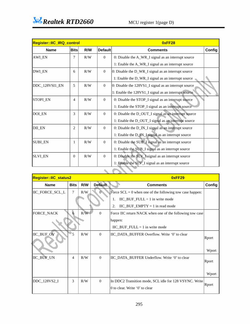
Realtek RTD2660 MCU register 1(page D)
295
Register::IIC_IRQ_control 0xFF28
Name Bits R/W Default Comments Config
AWI_EN 7 R/W 0 0: Disable the A_WR_I signal as an interrupt source
1: Enable the A_WR_I signal as an interrupt source
DWI_EN 6 R/W 0 0: Disable the D_WR_I signal as an interrupt source
1: Enable the D_WR_I signal as an interrupt source
DDC_128VSI1_EN 5 R/W 0 0: Disable the 128VS1_I signal as an interrupt source
1: Enable the 128VS1_I signal as an interrupt source
STOPI_EN 4 R/W 0 0: Disable the STOP_I signal as an interrupt source
1: Enable the STOP_I signal as an interrupt source
DOI_EN 3 R/W 0 0: Disable the D_OUT_I signal as an interrupt source
1: Enable the D_OUT_I signal as an interrupt source
DII_EN 2 R/W 0 0: Disable the D_IN_I signal as an interrupt source
1: Enable the D_IN_I signal as an interrupt source
SUBI_EN 1 R/W 0 0: Disable the SUB_I signal as an interrupt source
1: Enable the SUB_I signal as an interrupt source
SLVI_EN 0 R/W 0 0: Disable the SLV_I signal as an interrupt source
1: Enable the SLV_I signal as an interrupt source
Register::IIC_status2 0xFF29
Name Bits R/W Default Comments Config
IIC_FORCE_SCL_L 7 R/W 0 Force SCL = 0 when one of the following tow case happen:
1. IIC_BUF_FULL = 1 in write mode
2. IIC_BUF_EMPTY = 1 in read mode
FORCE_NACK 6 R/W 0 Force IIC return NACK when one of the following tow case
happen:
IIC_BUF_FULL = 1 in write mode
IIC_BUF_OV 5 R/W 0 IIC_DATA_BUFFER Overflow. Write ‘0’ to clear
Rport
Wport
IIC_BUF_UN 4 R/W 0 IIC_DATA_BUFFER Underflow. Write ‘0’ to clear
Rport
Wport
DDC_128VS2_I 3 R/W 0 In DDC2 Transition mode, SCL idle for 128 VSYNC. Write
0 to clear. Write ‘0’ to clear Rport
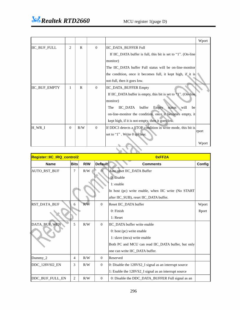
Realtek RTD2660 MCU register 1(page D)
296
Wport
IIC_BUF_FULL 2 R 0 IIC_DATA_BUFFER Full
If IIC_DATA buffer is full, this bit is set to “1”. (On-line
monitor)
The IIC_DATA buffer Full status will be on-line-monitor
the condition, once it becomes full, it kept high, if it is
not-full, then it goes low.
IIC_BUF_EMPTY 1 R 0 IIC_DATA_BUFFER Empty
If IIC_DATA buffer is empty, this bit is set to “1”. (On-line
monitor)
The IIC_DATA buffer Empty status will be
on-line-monitor the condition, once it becomes empty, it
kept high, if it is not-empty, then it goes low.
H_WR_I 0 R/W 0 If DDC3 detects a STOP condition in write mode, this bit is
set to “1” . Write 0 to clear. rport
Wport
Register::IIC_IRQ_control2 0xFF2A
Name Bits R/W Default Comments Config
AUTO_RST_BUF 7 R/W 0 Auto reset IIC_DATA Buffer
0: disable
1: enable
In host (pc) write enable, when IIC write (No START
after IIC_SUB), reset IIC_DATA buffer.
RST_DATA_BUF 6 R/W 0 Reset IIC_DATA buffer
0: Finish
1: Reset
Wport
Rport
DATA_BUF_WEN 5 R/W 0 IIC_DATA buffer write enable
0: host (pc) write enable
1: slave (mcu) write enable
Both PC and MCU can read IIC_DATA buffer, but only
one can write IIC_DATA buffer.
Dummy_2 4 R/W 0 Reserved
DDC_128VSI2_EN 3 R/W 0 0: Disable the 128VS2_I signal as an interrupt source
1: Enable the 128VS2_I signal as an interrupt source
DDC_BUF_FULL_EN 2 R/W 0 0: Disable the DDC_DATA_BUFFER Full signal as an

Realtek RTD2660 MCU register 1(page D)
297
interrupt source
1: Enable the DDC_DATA_BUFFER Full signal as an
interrupt source
DDC_BUF_EMPTY_EN 1 R/W 0 0: Disable the DDC_DATA_BUFFER Empty signal as
an interrupt source
1: Enable the DDC_DATA_BUFFER Empty signal as
an interrupt source
HWI_EN 0 R/W 0 0: Disable the H_WR_I signal as an interrupt source
1: Enable the H_WR_I signal as an interrupt source
Register::IIC_channel_control 0xFF2B
Name Bits R/W Default Comments Config
Reserved 7:2 -- 0 Reserved
RLS_SCL_SU 1 R/W 0 Set IIC data Setup Time When holding SCL low
0: Use Delay Chain (~5ns)
1: Use Crystal Clock to increase data setup time relative to
SCL clock line
HCH_SEL 0 R/W 0 Channel Select of DDC-CI
1: from DDC3
0: controlled by CH_SEL
Register:: DDC3_enable 0xFF2C
Name Bits R/W Default Comments Config
H_DDC_ADDR 7:5 R/W 0 DDC3 Channel Address Least Significant 3 Bits
(The default DDC channel address MSB 4 Bits is
“A”)
D_SCL_DBN_SEL 4 R/W 0 SCL Debounce Clock Selection
1: De-bounce reference clock
0: De-bounce clock (after clock divider)
H_DDC_W_STA 3 R/W 0 DDC3 Write Status (for external DDC access only)
It is cleared after write. Rport
Wport
H_DDCRAM_W_EN 2 R/W 0 DDC3 SRAM Write Enable (for external DDC
access only)

Realtek RTD2660 MCU register 1(page D)
298
0: Disable
1: Enable
H_DBN_EN 1 R/W 1 DDC3 De-bounce Enable
0: Disable
1: Enable (with crystal/4)
H_DDC_EN 0 R/W 0 DDC3 Channel Enable Bit
0: MCU access Enable
1: DDC channel Enable
Register:: DDC3_control_1 0xFF2D
Name Bits R/W Default Comments Config
H_DBN_CLK_SEL 7:6 R/W 0 De-bounce clock divider
00: 1/1 reference clock
01: 1/2 reference clock
1X: 1/4 reference clock
H_STOP_DBN_SEL 5:4 R/W 0 De-bounce sda stage
0X: latch one stage
10: latch two stage
11: latch three stage
H_SYS_CK_SEL 3 R/W 0 De-bounce reference clock
0: crystal clock
1. Serial flash clock (M2PLL / Flash_DIV)
H_DDC2 2 R/W 0 Force to DDC3 to DDC2 mode
0: Normal operation
1: DDC2 is active
RST_H_DDC 1 R/W 0 Reset DDC3 circuit
0: Normal operation
1: reset (auto cleared)
Rport
Wport
RVT_H_DDC1_EN 0 R/W 0 DDC3 revert to DDC1 enable(SCL idle for 128 VSYNC)
0: Disable
1: Enable
Register::DDC3_control_2 0xFF2E
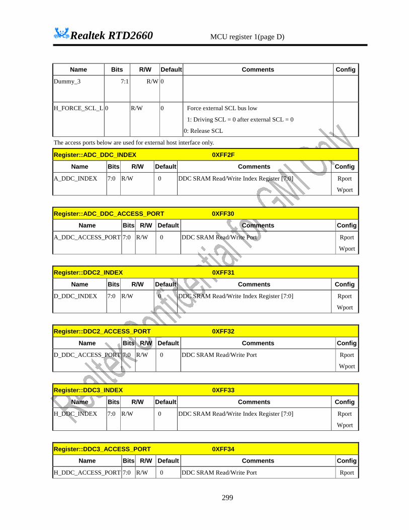
Realtek RTD2660 MCU register 1(page D)
299
Name Bits R/W Default Comments Config
Dummy_3 7:1 R/W 0
H_FORCE_SCL_L 0 R/W 0 Force external SCL bus low
1: Driving SCL = 0 after external SCL = 0
0: Release SCL
The access ports below are used for external host interface only.
Register::ADC_DDC_INDEX 0XFF2F
Name Bits R/W Default Comments Config
A_DDC_INDEX 7:0 R/W 0 DDC SRAM Read/Write Index Register [7:0] Rport
Wport
Register::ADC_DDC_ACCESS_PORT 0XFF30
Name Bits R/W Default Comments Config
A_DDC_ACCESS_PORT 7:0 R/W 0 DDC SRAM Read/Write Port Rport
Wport
Register::DDC2_INDEX 0XFF31
Name Bits R/W Default Comments Config
D_DDC_INDEX 7:0 R/W 0 DDC SRAM Read/Write Index Register [7:0] Rport
Wport
Register::DDC2_ACCESS_PORT 0XFF32
Name Bits R/W Default Comments Config
D_DDC_ACCESS_PORT 7:0 R/W 0 DDC SRAM Read/Write Port Rport
Wport
Register::DDC3_INDEX 0XFF33
Name Bits R/W Default Comments Config
H_DDC_INDEX 7:0 R/W 0 DDC SRAM Read/Write Index Register [7:0] Rport
Wport
Register::DDC3_ACCESS_PORT 0XFF34
Name Bits R/W Default Comments Config
H_DDC_ACCESS_PORT 7:0 R/W 0 DDC SRAM Read/Write Port Rport

Realtek RTD2660 MCU register 1(page D)
300
Wport
PWM
RTD2662 supports 6 channels of PWM DAC. The resolution of each PWM is 12-bit. PWM0, PWM1, PWM2, PWM3, PWM4 and PWM5 are connected to DA0, DA1, DA2, DA3, DA4 and DA5 respectively. The figure below represents the PWM clock generator. Based on the clock, we make up the PWM waveform which frequency is 1/4096 of the PWM clock. The PWM duty registers have 12-bit resolution. These registers have double buffer mechanism. When write the MSB bit, the 12-bit data will be loaded. The PWM frequency is :
Fpwm= fclk /2M /(N+1) /4096
The PWM frequency range is : fclk=27M, fpwm = 6.6KHz ~ 0.2Hz fclk=243M, fpwm = 60KHz ~ 1.8Hz
1/2M 1/(N+1)
OSC
PLL
PWM clock generator
first stage output second stage
output
243Mhz
27Mhz
fclk
Register::PWM_CK_SEL 0xFF3A
Name Bits R/W Default Comments Config
PWM_CK_SEL_DUMMY 7:6 R/W 0 dummy
PWM5_CK_SEL 5 R/W 0 PWMx clock generator input source
0: Crystal 1: PLL output
PWM4_CK_SEL 4 R/W 0 PWMx clock generator input source
0: Crystal 1: PLL output
PWM3_CK_SEL 3 R/W 0 PWMx clock generator input source
0: Crystal 1: PLL output
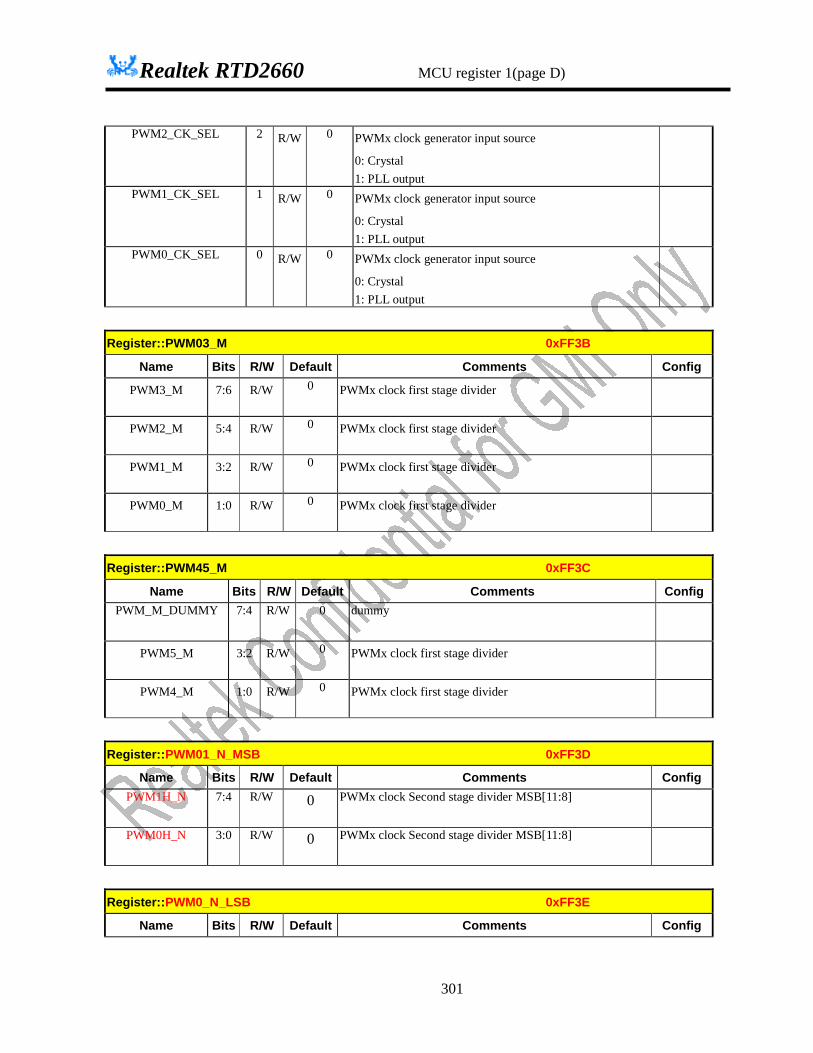
Realtek RTD2660 MCU register 1(page D)
301
PWM2_CK_SEL 2 R/W 0 PWMx clock generator input source
0: Crystal 1: PLL output
PWM1_CK_SEL 1 R/W 0 PWMx clock generator input source
0: Crystal 1: PLL output
PWM0_CK_SEL 0 R/W 0 PWMx clock generator input source
0: Crystal 1: PLL output
Register::PWM03_M 0xFF3B
Name Bits R/W Default Comments Config
PWM3_M 7:6 R/W 0 PWMx clock first stage divider
PWM2_M 5:4 R/W 0 PWMx clock first stage divider
PWM1_M 3:2 R/W 0 PWMx clock first stage divider
PWM0_M 1:0 R/W 0 PWMx clock first stage divider
Register::PWM45_M 0xFF3C
Name Bits R/W Default Comments Config PWM_M_DUMMY 7:4 R/W 0 dummy
PWM5_M 3:2 R/W 0 PWMx clock first stage divider
PWM4_M 1:0 R/W 0 PWMx clock first stage divider
Register::PWM01_N_MSB 0xFF3D
Name Bits R/W Default Comments Config PWM1H_N 7:4 R/W 0 PWMx clock Second stage divider MSB[11:8]
PWM0H_N 3:0 R/W 0 PWMx clock Second stage divider MSB[11:8]
Register::PWM0_N_LSB 0xFF3E
Name Bits R/W Default Comments Config
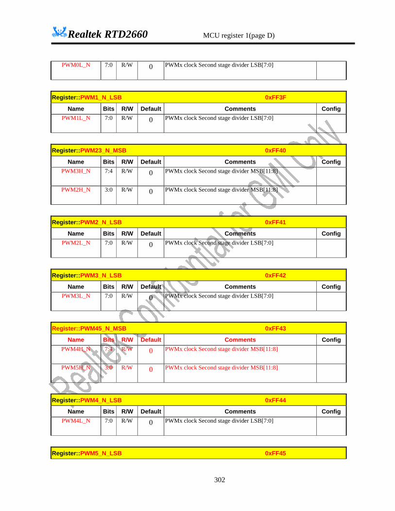
Realtek RTD2660 MCU register 1(page D)
302
PWM0L_N 7:0 R/W 0 PWMx clock Second stage divider LSB[7:0]
Register::PWM1_N_LSB 0xFF3F
Name Bits R/W Default Comments Config PWM1L_N 7:0 R/W 0 PWMx clock Second stage divider LSB[7:0]
Register::PWM23_N_MSB 0xFF40
Name Bits R/W Default Comments Config PWM3H_N 7:4 R/W 0 PWMx clock Second stage divider MSB[11:8]
PWM2H_N 3:0 R/W 0 PWMx clock Second stage divider MSB[11:8]
Register::PWM2_N_LSB 0xFF41
Name Bits R/W Default Comments Config PWM2L_N 7:0 R/W 0 PWMx clock Second stage divider LSB[7:0]
Register::PWM3_N_LSB 0xFF42
Name Bits R/W Default Comments Config PWM3L_N 7:0 R/W 0 PWMx clock Second stage divider LSB[7:0]
Register::PWM45_N_MSB 0xFF43
Name Bits R/W Default Comments Config PWM4H_N 7:4 R/W 0 PWMx clock Second stage divider MSB[11:8]
PWM5H_N 3:0 R/W 0 PWMx clock Second stage divider MSB[11:8]
Register::PWM4_N_LSB 0xFF44
Name Bits R/W Default Comments Config PWM4L_N 7:0 R/W 0 PWMx clock Second stage divider LSB[7:0]
Register::PWM5_N_LSB 0xFF45
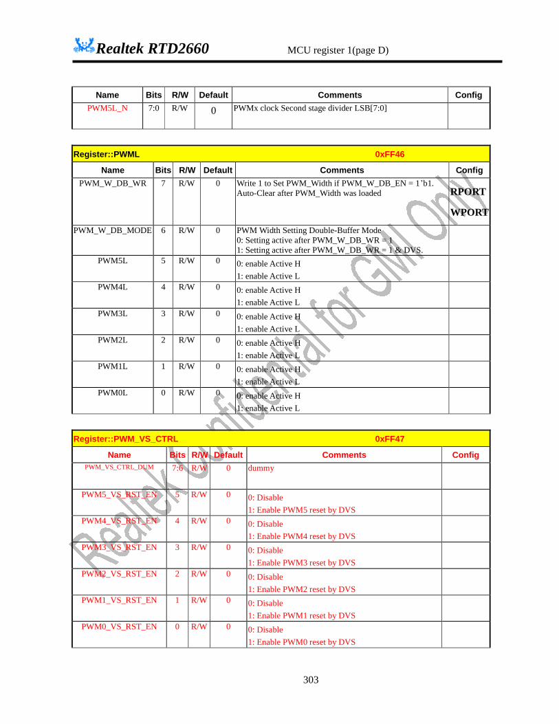
Realtek RTD2660 MCU register 1(page D)
303
Name Bits R/W Default Comments Config PWM5L_N 7:0 R/W 0 PWMx clock Second stage divider LSB[7:0]
Register::PWML 0xFF46
Name Bits R/W Default Comments Config PWM_W_DB_WR 7 R/W 0 Write 1 to Set PWM_Width if PWM_W_DB_EN = 1’b1.
Auto-Clear after PWM_Width was loaded RPORT
WPORT
PWM_W_DB_MODE 6 R/W 0 PWM Width Setting Double-Buffer Mode 0: Setting active after PWM_W_DB_WR = 1 1: Setting active after PWM_W_DB_WR = 1 & DVS.
PWM5L 5 R/W 0 0: enable Active H 1: enable Active L
PWM4L 4 R/W 0 0: enable Active H 1: enable Active L
PWM3L 3 R/W 0 0: enable Active H 1: enable Active L
PWM2L 2 R/W 0 0: enable Active H 1: enable Active L
PWM1L 1 R/W 0 0: enable Active H 1: enable Active L
PWM0L 0 R/W 0 0: enable Active H 1: enable Active L
Register::PWM_VS_CTRL 0xFF47
Name Bits R/W Default Comments Config PWM_VS_CTRL_DUM 7:6 R/W 0 dummy
PWM5_VS_RST_EN 5 R/W 0 0: Disable 1: Enable PWM5 reset by DVS
PWM4_VS_RST_EN 4 R/W 0 0: Disable 1: Enable PWM4 reset by DVS
PWM3_VS_RST_EN 3 R/W 0 0: Disable 1: Enable PWM3 reset by DVS
PWM2_VS_RST_EN 2 R/W 0 0: Disable 1: Enable PWM2 reset by DVS
PWM1_VS_RST_EN 1 R/W 0 0: Disable 1: Enable PWM1 reset by DVS
PWM0_VS_RST_EN 0 R/W 0 0: Disable 1: Enable PWM0 reset by DVS
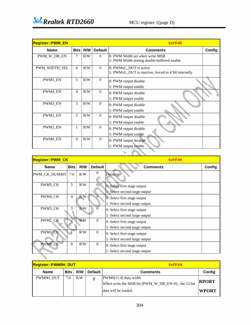
Realtek RTD2660 MCU register 1(page D)
304
Register::PWM_EN 0xFF48
Name Bits R/W Default Comments Config PWM_W_DB_EN 7 R/W 0 0: PWM Width set when write MSB
1: PWM Width setting double-buffered enable
PWM_WIDTH_SEL 6 R/W 0 0: PWMxL_DUT is active 1: PWMxL_DUT is inactive, forced to 4’h0 internally
PWM5_EN 5 R/W 0 0: PWM output disable 1: PWM output enable
PWM4_EN 4 R/W 0 0: PWM output disable 1: PWM output enable
PWM3_EN 3 R/W 0 0: PWM output disable 1: PWM output enable
PWM2_EN 2 R/W 0 0: PWM output disable 1: PWM output enable
PWM1_EN 1 R/W 0 0: PWM output disable 1: PWM output enable
PWM0_EN 0 R/W 0 0: PWM output disable 1: PWM output enable
Register::PWM_CK 0xFF49
Name Bits R/W Default Comments Config
PWM_CK_DUMMY 7:6 R/W 0 Dummy
PWM5_CK 5 R/W 0 0: Select first stage output 1: Select second stage output
PWM4_CK 4 R/W 0 0: Select first stage output 1: Select second stage output
PWM3_CK 3 R/W 0 0: Select first stage output 1: Select second stage output
PWM2_CK 2 R/W 0 0: Select first stage output 1: Select second stage output
PWM1_CK 1 R/W 0 0: Select first stage output 1: Select second stage output
PWM0_CK 0 R/W 0 0: Select first stage output 1: Select second stage output
Register::PWM0H_DUT 0xFF4A
Name Bits R/W Default Comments Config PWM0H_DUT 7:0 R/W 0 PWM0[11:4] duty width
When write the MSB bit (PWM_W_DB_EN=0) , the 12-bit
data will be loaded.
RPORT
WPORT

Realtek RTD2660 MCU register 1(page D)
305
Register::PWM1H_DUT 0xFF4B
Name Bits R/W Default Comments Config PWM1H_DUT 7:0 R/W 0 PWM1[11:4] duty width
When write the MSB bit (PWM_W_DB_EN=0) , the 12-bit data will be loaded.
RPORT
WPORT
Register::PWM01L_DUT 0xFF4C
Name Bits R/W Default Comments Config PWM1L_DUT 7:4 R/W 0 PWM1[3:0] duty width
RPORT
WPORT
PWM0L_DUT 3:0 R/W 0 PWM0[3:0] duty width RPORT
WPORT
Register::PWM2H_DUT 0xFF4D
Name Bits R/W Default Comments Config PWM2H_DUT 7:0 R/W 0 PWM2[11:4] duty width
When write the MSB bit (PWM_W_DB_EN=0) , the 12-bit data will be loaded.
RPORT
WPORT
Register::PWM3H_DUT 0xFF4E
Name Bits R/W Default Comments Config PWM3H_DUT 7:0 R/W 0 PWM3[11:4] duty width
When write the MSB bit (PWM_W_DB_EN=0) , the 12-bit data will be loaded.
RPORT
WPORT
Register::PWM23L_DUT 0xFF4F
Name Bits R/W Default Comments Config PWM3L_DUT 7:4 R/W 0 PWM3[3:0] duty width
RPORT
WPORT
PWM2L_DUT 3:0 R/W 0 PWM2[3:0] duty width RPORT
WPORT
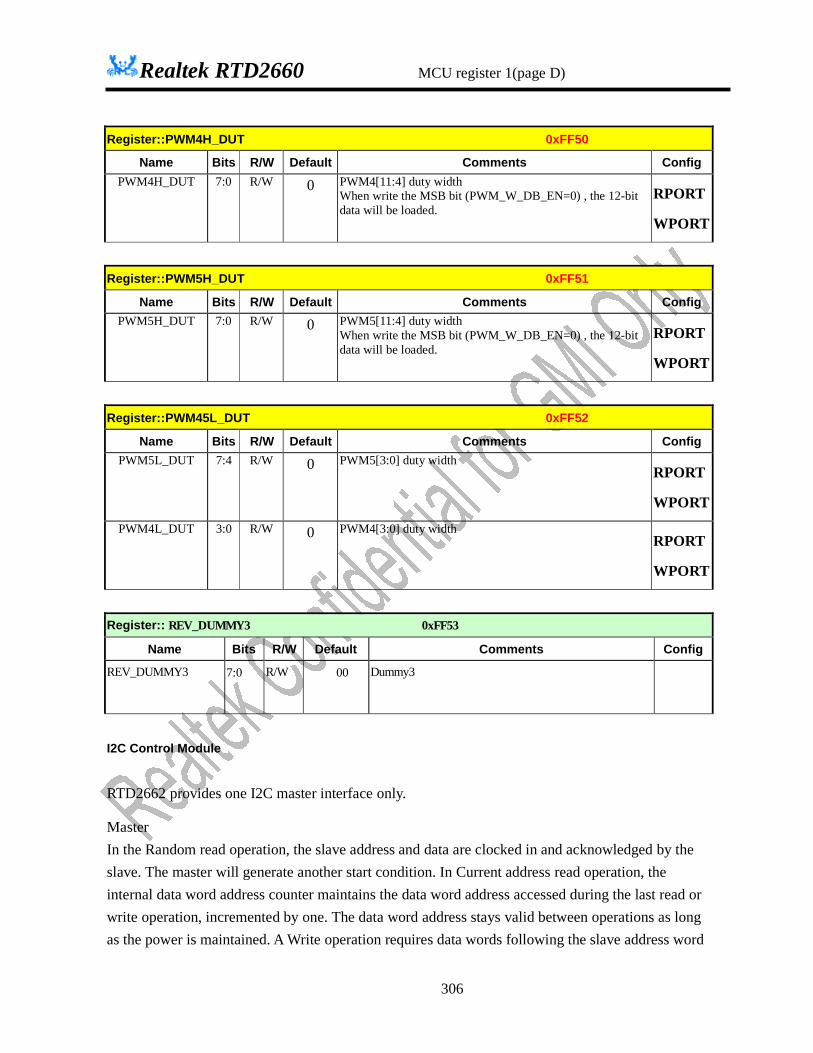
Realtek RTD2660 MCU register 1(page D)
306
Register::PWM4H_DUT 0xFF50
Name Bits R/W Default Comments Config PWM4H_DUT 7:0 R/W 0 PWM4[11:4] duty width
When write the MSB bit (PWM_W_DB_EN=0) , the 12-bit data will be loaded.
RPORT
WPORT
Register::PWM5H_DUT 0xFF51
Name Bits R/W Default Comments Config PWM5H_DUT 7:0 R/W 0 PWM5[11:4] duty width
When write the MSB bit (PWM_W_DB_EN=0) , the 12-bit data will be loaded.
RPORT
WPORT
Register::PWM45L_DUT 0xFF52
Name Bits R/W Default Comments Config PWM5L_DUT 7:4 R/W 0 PWM5[3:0] duty width
RPORT
WPORT
PWM4L_DUT 3:0 R/W 0 PWM4[3:0] duty width RPORT
WPORT
Register:: REV_DUMMY3 0xFF53
Name Bits R/W Default Comments Config
REV_DUMMY3 7:0 R/W 00 Dummy3
I2C Control Module
RTD2662 provides one I2C master interface only.
Master In the Random read operation, the slave address and data are clocked in and acknowledged by the slave. The master will generate another start condition. In Current address read operation, the internal data word address counter maintains the data word address accessed during the last read or write operation, incremented by one. The data word address stays valid between operations as long as the power is maintained. A Write operation requires data words following the slave address word

Realtek RTD2660 MCU register 1(page D)
307
and acknowledgment. The master terminates the write sequence with a stop condition. In Write with restart operation, master will generate another start condition after transmitting the slave address and data. If slave needs stop condition between data and restart command (Sr) in the Random read operation, software can transmit the Current address read operation following A Write operation. The maximum value of data FIFO (N) is 24. The slave address byte will be written into FIFO register together with data. Software must write the eighth bit of slave address byte to decide the access is read or write. NOTE: (a) RTD2660 only supports master function (b) RTD2660 doesn’t support arbitration mechanism while one system exists over 2 masters (c) FIFO can’t support R/W at the same time. It means that you can’t transmit data successively
while the byte counts over 24, since MCU have to refresh the FIFO data for the next transmit (d) Master supports the function that slave can hold SCL to zero after ACK when slave can’t give
master data that master wanted.
Signal Name Type Function Note
SCL O
SDA I/O
Register:: I2CM_CR0 0xFF55
Name Bits R/W Default Comments Config
IICM_SW_RSTN
7 R/W 0 IIC master software reset
0: Reset, Blocking IICM module
1: Enable IICM module
CS 6 R/W 0 Command Start
0 = Stop, after completing whole transaction, it returns to
zero
1 = Start
wport
rport
RWL 5:1 R/W 0 Read/Write data Length for related commands. Not includes slave address byte in FIFO register. When access, controller will parse the byte followed last start (or Sr) byte to know the command type. 0x00 = 1 bytes
:

Realtek RTD2660 MCU register 1(page D)
308
0x17 = 24 bytes
TORE 0 R/W 1 TOR enable
If TOR is desired, I2C rate must be constrained form 25kb/s~ 400kb/s. This constraint is due to the time-out register bit.
Register:: I2CM_CR1 0xFF56
Name Bits R/W Default Comments Config
TOR 7:0 R/W 0x3A Time-out register
Time-out = TOR x 2 x ((FD10+1)/input clock) (For receive
/transmit one bit)
If time-out occur, it will trigger Transaction Error Interrupt
Flag
Note: time-out must > (1 SCL low period + repeat start
setup time)
Register:: I2CM_CR2 0xFF57
Name Bits R/W Default Comments Config
reserved 7 - 0 Reserved to 0
BURST 6 R/W 0 Burst mode enabled to write over 24 bytes to slave devices.
While burst is enabled, whole I2C will be halted to let MCU
write another more bytes to FIFO. After the job done, we
have to set I2CM_SR to be high to continue the I2C write job
SBAIFD 5 R/W 0 Reserved
FBAIFD 4 R/W 0 Reserved
SRSIB 3:2 R/W 0 Reserved
FRSIB 1:0 R/W 0 Reserved
Register:: I2CM_CR3 0xFF58
Name Bits R/W Default Comments Config
reserved 7:5 - 0 Reserved to 0
RSC 4:3 R/W 0 Repeat start count 00: No repeat start 01: one repeat start 10: two repeat start

Realtek RTD2660 MCU register 1(page D)
309
11: forbidden TEIE 2 R/W 0 Transaction Error Interrupt Enable
MRCIE 1 R/W 0 Master Receive complete Interrupt Enable
MTCIE 0 R/W 0 This Interrupt enable bit serve two conditions, one is “Master Transmit complete Interrupt Enable in single mode” and the other is “Master Transmit partial Done Interrupt Enable in burst mode”
Register:: I2CM_STR0 0xFF59
Name Bits R/W Default Comments Config
reserved 7 - 0 Reserved to 0
I2CMD 6:4 R/W 0 I2C master debounce
0: sample rate=(input clk / (FD10+1) )
1: sample rate=(input clk / (FD10+1) ) / 2
:
7: sample rate= (input clk / (FD10+1) ) / 8
FTPC 3:0 R/W 0x3 Fall time period count
If the value of (Bus clock/FD10) does not approximate
10Mhz, FTPC can make sure that fall time of SCL is more
than 300ns.
Register:: I2CM_STR1 0xFF5A
Name Bits R/W Default Comments Config
STA_SUGPIO_C 7:0 R/W 0x09 STA setup time period count
In repeat start, the setup time of SCL must match the I2C
spec.
Register:: I2CM_STR2 0xFF5B
Name Bits R/W Default Comments Config
SHPC 7:0 R/W 0x09 SCL high period counter
(SCL High period=100ns*SHPC)
SHPC must include rising time in the I2C spec.
Register:: I2CM_STR3 0xFF5C

Realtek RTD2660 MCU register 2(page E)
310
Name Bits R/W Default Comments Config
SLPC 7:0 R/W 0x10 SCL low period counter
(SCL low period=100ns*SLPC)
SLPC must include falling time in the I2C spec.
Register:: I2CM_SR 0xFF5D
Name Bits R/W Default Comments Config
reserved 7:5 - 0 Reserved to 0
BSA 4 R/W 0 Send again Control bit in burst mode 1: Send 0: Not action Write “1” to clear
wport
rport
BMPIF 3 R/W 0 Burst Mode Pending Interrupt Flag While setting as burst mode and I2C master transmit data in TDD, this flag is asserted. Write “1” to clear
wport
rport
TEIF 2 R/W 0 Transaction Error Interrupt Flag When master transmit/receive fault or time-out occurrence, I2C controller will lift the flag up and return to bus idle. Write “1” to clear
wport
rport
MRCIF 1 R/W 0 Master Receive complete Interrupt flag Write “1” to clear
wport
rport
MTCIF 0 R/W 0 This Interrupt enable bit serves two conditions, one is “Master Transmit complete Interrupt Enable in single mode” and the other is “Master Transmit partial Done Interrupt Enable in burst mode” Write “1” to clear
wport
rport
Register:: I2CM_TD 0xFF5E
Name Bits R/W Default Comments Config
TDD 7:0 R/W 0 Target Device Data to receive or transmit wport
rport
Register:: I2CM_CCR 0xFF5F
Name Bits R/W Default Comments Config
reserved 7:6 - 0 Reserved to 0
FD10 5:0 R/W 0x03 Frequency 10M Divisor 0 are forbidden 10M=input clock/(FD10+1) When power on, software must write FD10 to let I2C controller generate ~10 Mhz clock.

Realtek RTD2660 MCU register 2(page E)
311
MCU register 2(page E)
SPI-FLASH
Common Instruction Register Register::common_inst_en 0xFF60
Name Bits R/W Default Comments Config
com_inst 7:5 R/W 0x0 000: no operation
001 : write
010 : Read
011 : write after WREN
100 : write after EWSR
101 : Erase
write_num 4:3 R/W 0x0 Common instruction write number
rd_num 2:1 R/W 0x0 Common instruction read number
com_inst_en 0 R/W 0x0 Common instruction enable (auto clear when finish) Wport Rport
Register::common_op_code 0xFF61
Name Bits R/W Default Comments Config
com_op 7:0 R/W 0x0 Common instruction op code
Register::wren_op_code 0xFF62
Name Bits R/W Default Comments Config
wren_op 7:0 R/W 0x06 Write enable op code
Register::ewsr_op_code 0xFF63
Name Bits R/W Default Comments Config

Realtek RTD2660 MCU register 2(page E)
312
ewsr_op 7:0 R/W 0x50 Enable write register op code
Register::Flash_prog_ISP0 0xFF64
Name Bits R/W Default Comments Config
prog_h 7:0 R/W 0x00 Flash program/write/dummy/read CRC high byte[23:16] Wport
Rport
Register::Flash_prog_ISP1 0xFF65
Name Bits R/W Default Comments Config
prog_m 7:0 R/W 0x00 Flash program/write/dummy/read CRC middle
byte[15:8]
Wport
Rport
Register::Flash_prog_ISP2 0xFF66
Name Bits R/W Default Comments Config
prog_l 7:0 R/W 0x00 Flash program/write/dummy/read CRC low byte[7:0] Wport
Rport
Register::common_inst_read_port0 0xFF67
Name Bits R/W Default Comments Config
com_rd_h 7:0 R 0x00 Common instruction read high byte[23:16]
Register::common_inst_read_port1 0xFF68
Name Bits R/W Default Comments Config
com_rd_m 7:0 R 0x00 Common instruction read middle byte[15:8]
Register::common_inst_read_port2 0xFF69
Name Bits R/W Default Comments Config
com_rd_l 7:0 R 0x00 Common instruction read low byte[7:0]
Common Instruction Usage :
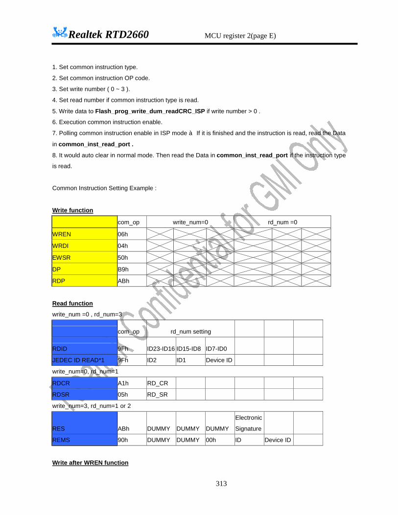
Realtek RTD2660 MCU register 2(page E)
313
1. Set common instruction type.
2. Set common instruction OP code.
3. Set write number ( 0 ~ 3 ).
4. Set read number if common instruction type is read.
5. Write data to Flash_prog_write_dum_readCRC_ISP if write number > 0 .
6. Execution common instruction enable.
7. Polling common instruction enable in ISP mode à If it is finished and the instruction is read, read the Data
in common_inst_read_port .
8. It would auto clear in normal mode. Then read the Data in common_inst_read_port if the instruction type
is read.
Common Instruction Setting Example :
Write function
com_op write_num=0 rd_num =0
WREN 06h
WRDI 04h
EWSR 50h
DP B9h
RDP ABh
Read function
write_num =0 , rd_num=3
com_op rd_num setting
RDID 9Fh ID23-ID16 ID15-ID8 ID7-ID0
JEDEC ID READ*1 9Fh ID2 ID1 Device ID
write_num=0, rd_num=1
RDCR A1h RD_CR
RDSR 05h RD_SR
write_num=3, rd_num=1 or 2
RES ABh DUMMY DUMMY DUMMY
Electronic
Signature
REMS 90h DUMMY DUMMY 00h ID Device ID
Write after WREN function
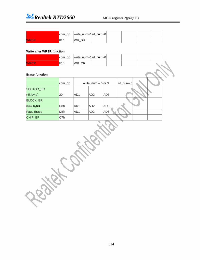
Realtek RTD2660 MCU register 2(page E)
314
com_op write_num=1 rd_num=0
WRSR 01h WR_SR
Write after WRSR function
com_op write_num=1 rd_num=0
WRCR F1h WR_CR
Erase function
com_op write_num = 0 or 3 rd_num=0
SECTOR_ER
(4k byte) 20h AD1 AD2 AD3
BLOCK_ER
(64k byte) D8h AD1 AD2 AD3
Page Erase DBh AD1 AD2 AD3
CHIP_ER C7h

Realtek RTD2660 MCU register 2(page E)
315
Program/Read/ISP/CRC Register Register::read_op_code 0xFF6A
Name Bits R/W Default Comments Config
read_op 7:0 R/W 0x03 Read command op code Wen_out
Note : 1 It would force flash controller to idle state when write this byte.
Register::fast_read_op_code 0xFF6B
Name Bits R/W Default Comments Config
Fast_read_op 7:0 R/W 0x0B Fast read command op code Wen_out
Note : 1 It would force flash controller to idle state when write this byte.
Register::read_instruction 0xFF6C
Name Bits R/W Default Comments Config
read_mode 7:6 R/W 0x0 00: normal read
01: fast read
10: fast dual data read
Wen_out
latch_so_rise 5 R/W 0x0 0: latch Flash SO Data in rising edge
1: latch Flash SO Data in falling edge Wen_out
drive_si_fall 4 R/W 0x0 0: Output Flash SI Data in falling edge
1: Output Flash SI Data in rising edge Wen_out
si_dly_sel 3:2 R/W 0x0 00: 0ns 01: 2ns
10: 4ns 11: 6ns Wen_out
so_dly_sel 1:0 R/W 0x0 00: 0ns 01: 2ns
10: 4ns 11: 6ns Wen_out
Note: 1. Normally, SPI Flash drive data in falling edge and sample data in rising edge !!!!
2. It would force flash controller to idle state when write this byte.
Register::program_op_code 0xFF6D
Name Bits R/W Default Comments Config
prog_op 7:0 R/W 0x02 Program command op code
Register::read_status_register_op_code 0xFF6E

Realtek RTD2660 MCU register 2(page E)
316
Name Bits R/W Default Comments Config
rdsr_op 7:0 R/W 0x05 Read status register register command op code
Register::program_instruction 0xFF6F
Name Bits R/W Default Comments Config
isp_en 7 R/W 0x0 Enable ISP program : all registers except this register
can’t write/read when ISP_ENABLE=0
0: disable
1: enable (gating 8051 clock)
Rport
Wport
prog_mode 6 R/W 0x0 0: normal mode
1: AAI mode
prog_en 5 R/W 0x0 0: finish
1: program on-going (write 1 to start, auto clear when
finish)
Rport
Wport
prog_buf_wr_en 4 R 0x1 0: can’t write data to sram
1: can write data to sram
prog_dummy 3 R/W 0x0
crc_start 2 R/W 0x0 When write one, read data from PROG_ST_ADDR to PROG_END_ADDR. And at the same time the CRC is calculated by IC automatically.
This bit will be auto cleared when crc_done is 1.(Can be trigger in ISP Mode only)
Rport
Wport
crc_done 1 R 0x1 It will show 1 when CRC is done, and will return to 0
when CRC_START is set.
rst_flash_ctrl 0 R/W 0x0 0: disable
1: software reset flash controller
Rport
Wport
No Use Parser::program_data_port 0xFF70
Name Bits R/W Default Comments Config
prog_port 7:0 W Program write data port to SRAM
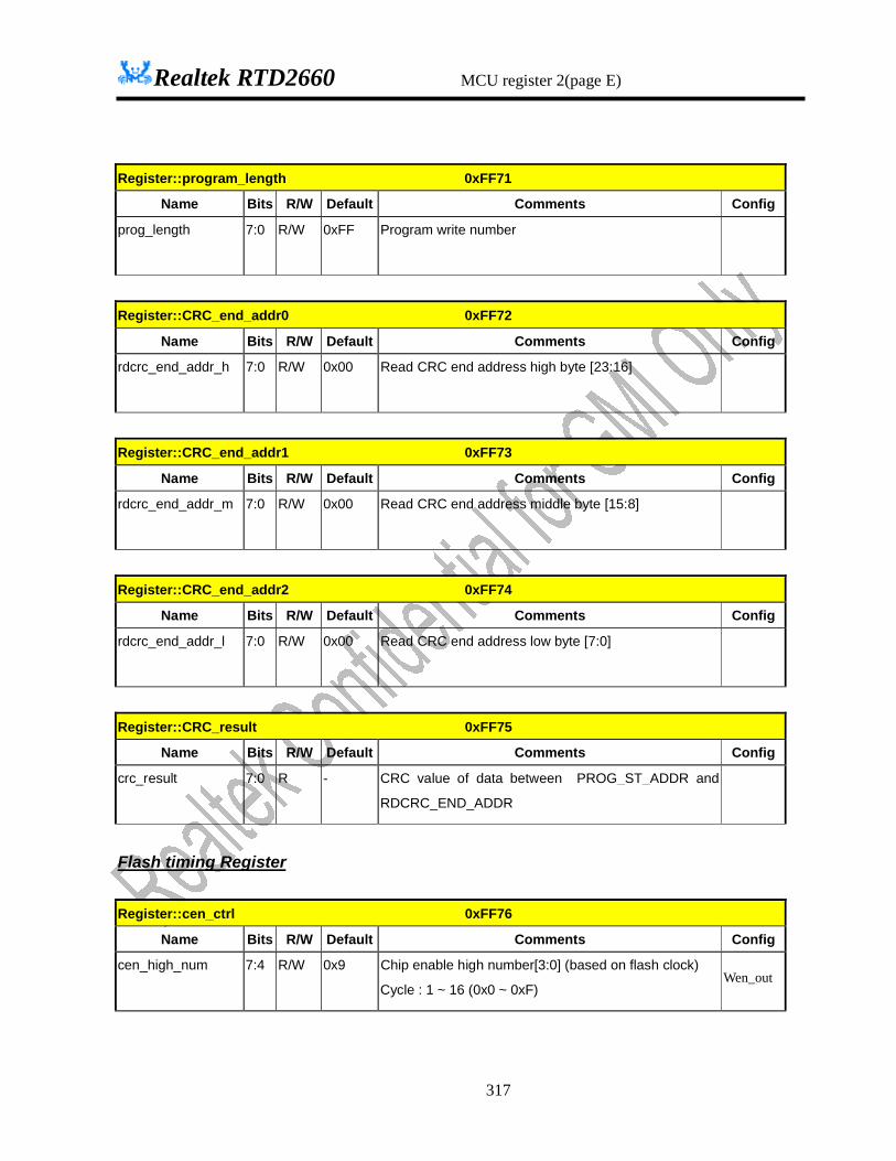
Realtek RTD2660 MCU register 2(page E)
317
Register::program_length 0xFF71
Name Bits R/W Default Comments Config
prog_length 7:0 R/W 0xFF Program write number
Register::CRC_end_addr0 0xFF72
Name Bits R/W Default Comments Config
rdcrc_end_addr_h 7:0 R/W 0x00 Read CRC end address high byte [23:16]
Register::CRC_end_addr1 0xFF73
Name Bits R/W Default Comments Config
rdcrc_end_addr_m 7:0 R/W 0x00 Read CRC end address middle byte [15:8]
Register::CRC_end_addr2 0xFF74
Name Bits R/W Default Comments Config
rdcrc_end_addr_l 7:0 R/W 0x00 Read CRC end address low byte [7:0]
Register::CRC_result 0xFF75
Name Bits R/W Default Comments Config
crc_result 7:0 R - CRC value of data between PROG_ST_ADDR and
RDCRC_END_ADDR
Flash timing Register
Register::cen_ctrl 0xFF76
Name Bits R/W Default Comments Config
cen_high_num 7:4 R/W 0x9 Chip enable high number[3:0] (based on flash clock)
Cycle : 1 ~ 16 (0x0 ~ 0xF) Wen_out
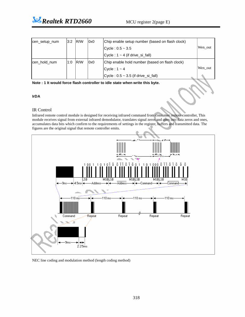
Realtek RTD2660 MCU register 2(page E)
318
cen_setup_num 3:2 R/W 0x0 Chip enable setup number (based on flash clock)
Cycle : 0.5 ~ 3.5
Cycle : 1 ~ 4 (if drive_si_fall)
Wen_out
cen_hold_num 1:0 R/W 0x0 Chip enable hold number (based on flash clock)
Cycle : 1 ~ 4
Cycle : 0.5 ~ 3.5 (if drive_si_fall)
Wen_out
Note : 1 It would force flash controller to idle state when write this byte.
IrDA
IR Control Infrared remote control module is designed for receiving infrared command from consumer remote controller, This module receives signal from external infrared demodulator, translates signal zeros and ones into data zeros and ones, accumulates data bits which confirm to the requirements of settings in the register, buffers and transmitted data. The figures are the original signal that remote controller emits.
NEC line coding and modulation method (length coding method)

Realtek RTD2660 MCU register 2(page E)
319
RC-5 line coding and modulation method (phase coding method)
Register bus
Sampling base clockgenerator
IR read FIFO 48-bit x2
Control Unit & StatusInterrupt
IR RX

Realtek RTD2660 MCU register 2(page E)
320
Infrared control functional block diagram
RTD2662 provides a universal Infrared decoder that decodes mostly infrared coding method via programmable parameter set. Infrared decoder uses a programmable sampling clock generator to fit the infrared speed. The two layer 48-bit FIFO stores the infrared data. And an interrupt signal interrupts CPU when infrared data received.
Burst Length Silence LengthRepeatLength
Data Burst Length
Start Code definition
Infrared Signal Format
Start Code
bit0 bit1 bit2 bit3 bit n
Data
Repeat Code definition
RepeatCode
Idle
Infrared signal format definition
AS shown in the above figure, burst length and silence length define the start code, burst length and repeat length define the repeat code, data bit n defines the total valid bit number. And as show in the following figure, the modulation length, data one length and data zero length define the bit data format.
Phase Coding Method: Normal
Modulation Length
Modulation Length
Modulation Length
Modulation Length
Data Zero Data One
Data zero Data One
Modulation Length
Data ZeroLength
Data One Length
Length Coding Method: Normal
Modulation Length
Phase Coding Method: Invert
Modulation Length
Modulation Length
Modulation Length
Modulation Length
Data Zero Data One
Data zero Data One
Modulation Length
Data ZeroLength
Data One Length
Length Coding Method: Invert
Modulation Length
Infrared signal data bit definition
Register:: IR_Ctrl1 0xFF80
Name Bits R/W Default Comments Config sd_d_d_sd 7 R/W 0 Dummy
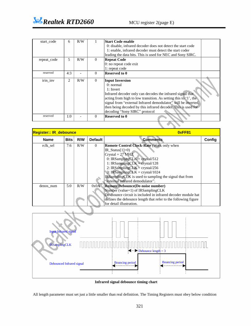
Realtek RTD2660 MCU register 2(page E)
321
start_code 6 R/W 1 Start Code enable 0: disable, infrared decoder does not detect the start code 1: enable, infrared decoder must detect the start coder leading the data bits. This is used for NEC and Sony SIRC.
repeat_code 5 R/W 0 Repeat Code 0: no repeat code exit 1: repeat code
reserved 4:3 - 0 Reserved to 0 irin_inv 2 R/W 0 Input Inversion
0: normal 1: Invert Infrared decoder only can decodes the infrared signal that acting from high to low transition. As setting this to ‘1’, the signal from “external Infrared demodulator” will be inverted, then being decoded by this infrared decoder. This is used for decoding “Sony SIRC” protocol
reserved 1:0 - 0 Reserved to 0
Register:: IR_debounce 0xFF81
Name Bits R/W Default Comments Config rclk_sel 7:6 R/W 0 Romote Control Clock-Rate (Work only when
IR_Status[1]=0) Crystal = 27 MHZ 0: IRSamplingCLK = crystal/512 1: IRSamplingCLK = crystal/128 2: IRSamplingCLK = crystal/256 3: IRSamplingCLK = crystal/1024 IRSamplingCLK is used to sampling the signal that from “external infrared demodulator”.
denos_num 5:0 R/W 0x0A Remote Debounce(De-noise number) Number (value+1) of IRSamplingCLK De-Bounce circuit is included in infrared decoder module hat defines the debounce length that refer to the following figure for detail illustration.
Bouncing period Bouncing period
Debounce length = 3
IRSamplingCLK
Input Infrared signal
Debounced Infrared signal
Infrared signal debounce timing chart
All length parameter must set just a little smaller than real definition. The Timing Registers must obey below condition
Realtek RTD2660 MCU register 2(page E)
322
1. IR_SlienceLen >< IR_RepeatLen 2. IR_Data0Len >< IR_Data1Len 3. IR_BurstLen > IR_Data0Len, IR_Data1Len
Register:: IR_Burst_Length 0xFF82
Name Bits R/W Default Comments Config burst_length 7:0 R/W 0x64 Remote burst length =(Value * 4) * IRSamplingCLK period
Register:: IR_Silence_Length 0xFF83
Name Bits R/W Default Comments Config silen_length 7:0 R/W 0x32 Remote silence length =(Value * 4) * IRSamplingCLK
period
Register:: IR_Repeat_Length 0xFF84
Name Bits R/W Default Comments Config rpt_length 7:0 R/W 0x19 Remote repeat length =(Value * 4) * IRSamplingCLK
period, for repeat command
Register:: IR_Mod_Length 0xFF85
Name Bits R/W Default Comments Config modu_length 7:0 R/W 0x19 Remote modulation length =Value * IRSamplingCLK
period
Register:: IR_Data0_Length 0xFF86
Name Bits R/W Default Comments Config data0_high 7:0 R/W 0x19 Remote data zero length =Value * IRSamplingCLK period
Register:: IR_Data1_Length 0xFF87
Name Bits R/W Default Comments Config data1_high 7:0 R/W 0x4C Remote data one length =Value *IRSamplingCLK period
Register:: IR_Ctrl2 0xFF88
Name Bits R/W Default Comments Config ph_len 7 R/W 1 Data Bit Coding Method
0: phase method 1: length method
ph_len_inv 6 R/W 0 Data Bit Coding Mode 0: normal 1: invert Bit 7 bit 6: 00: phase coding method normal mode
Realtek RTD2660 MCU register 2(page E)
323
01: phase coding method invert mode 10: length coding method normal mode 11: length coding method invert mode
data_num 5:0 R/W 0x1F Remote data number define number of bits of data (1~48)
Register:: IR_Status 0xFF89
Name Bits R/W Default Comments Config str_flag 7 R 0 Start Code flag (write 1 clear)
This bit will be set to ‘1’ when infrared decoder detects the Start Code.
Wclr_out
buf_ovf 6 R 0 Buffer Overflow flag 0: data buffer is not overflow 1: New IR data is received when all data buffers contain valid data. IR decoder will block IR data when Overflow flag is true. And Overflow flag is cleared automatically when any one of data buffer is empty.
rd_buf_sel 5 R 0 Read buffer select 0: read buffer 0 1: read buffer 1 This bit indicates which buffer that be read via “Remote Data Access Port”
buf1_flag 4 R 0 Buffer 1 flag 1: data valid This bit indicates buffer 1 has valid data or not.
buf0_flag 3 R 0 Buffer 0 flag 1: data valid This bit indicates buffer 0 has valid data or not
buf_rpt 2 R 0 Remote repeat event As infrared decoder detect “repeat code”, this bit will be set to 1. The repeat event is true only when repeat code immediately follows a normal command, i.e. the infrared sequence “idle + repeat code” will not assert repeat flag and this “repeat code” will be ignored. Infrared decoder implements two layer repeat flag to indicate the repeat event of buffer1 and buffer2 As “repeat code” occurs, the previous received infrared data will be push into current FIFO and asserts data valid flag. Remote repeat event is cleared when correspond data is read from IR_Dataport_MSB. Buf1 -> Buf2 or Buf2 -> Buf1
remote_tst 1 R/W 0 Remote test enable 0: selected IRSamplingCLK is set by IR_debounce[7:6] 1: IRSamplingCLK is crystal clock
ir_sw_rstn 0 R/W 0 Remote soft reset 0: Reset, Blocking IR module 1: Enable IR module
Register:: IR_Data0 0xFF8A
Name Bits R/W Default Comments Config BYTE0 7:0 R 0 Remote data read port [7:0]
From Buf1 or Buf2

Realtek RTD2660 MCU register 2(page E)
324
Register:: IR_Data1 0xFF8B
Name Bits R/W Default Comments Config BYTE1 7:0 R 0 Remote data read port [15:8]
From Buf1 or Buf2
Register:: IR_Data2 0xFF8C
Name Bits R/W Default Comments Config BYTE2 7:0 R 0 Remote data read port [23:16]
From Buf1 or Buf2
Register:: IR_Data3 0xFF8D
Name Bits R/W Default Comments Config BYTE3 7:0 R 0 Remote data read port [31:24]
From Buf1 or Buf2
Register:: IR_Data4 0xFF8E
Name Bits R/W Default Comments Config BYTE4 7:0 R 0 Remote data read port [39:32]
From Buf1 or Buf2
Register:: IR_Data5 0xFF8F
Name Bits R/W Default Comments Config BYTE5 7:0 R 0 Remote data read port [47:40]
From Buf1 or Buf2 rport
l The last bit (MSB) received is the MSB of data (port [47]) l Data valid and repeat flag is clear when the port [47:40] is read. l If data is less than 48bit, the MSB is in port [47]. Other un-used bits are in lower bits. Register:: IR_One_Cmd_Time 0xFF90
Name Bits R/W Default Comments Config one_cmd_time 7:0 R/W 0xA0 One Command Time =(Value * 32) * IRSamplingCLK
period. The One Command Time is counting start when infrared detect the start code or data bit. Once the Timer start counting, infrared decoder can decode next command until the Timer timeout. Infrared decoder granted only one infrared is decoded during the One Command Time interval. This is used to reject noise. The value of One Command Time is usually a little smaller than the command period. When One Command Time is smaller than total bit time, the IR decoder can decode the IR data continuously.
Register:: IR_Idle_Time 0xFF91

Realtek RTD2660 MCU register 2(page E)
325
Name Bits R/W Default Comments Config idle_time 7:0 R/W 0xA3 Idle Time =(Value * 32) * IRSamplingCLK_period.
The Idle Time is counting start when infrared detect the start code or data bit. Infrared decoder goes into idle state when Idle Time out. This is used to prevent wrong “repeat code” detection. The value of Idle Time is usually a little larger than the command period. As Idle Time is smaller than total bit time, all input “repeat code” are invalid. As Idle Time is equal to 0xFF, all input “repeat code” are valid without Idle Time constraint.
n n+1
Reject any new command in this period
One Command Time
Command Period
Idle Time
Repeat Code is invalidRepeat code is valide
Available for new cmd
Infrared signal Command Time and Idle Time
Register:: IR_Ctrl3 0xFF92
Name Bits R/W Default Comments Config DataNotEnough 7 R 0 Data Not Enough Event (write 1 clear)
This event happens when received data bit less than Data_num 0: normal. 1: Data Not Enough Event Occurred, write 1 to clear this flag
Wclr_out
RxDataNum 6:1 R 0 Received Data Number RxDataNum indicates received data number when DataNotEnough event happens. RxDataNum is cleared when write 1 to DataNotEnough
bit_swap 0 R/W 0 Bit Swap 0: The decoded IR bits is aligned to the MSB of IRDataPort. That means the last decode data is stored in the IRDataPort47] 1: The decode IR bits is aligned to the LSB of IRDataPort. That means the last decode data is stored in the IRDataPort[0].
Register:: IR_INTRQ 0xFF93
Name Bits R/W Default Comments Config reserved 7:4 - 0 Reserved to 0
flag0int_en 3 R/W 0 Buffer 0 data valid IRQ enable flag1int_en 2 R/W 0 Buffer 1 data valid IRQ enable rptint_en 1 R/W 0 Repeat event IRQ enable ovfint_en 0 R/W 0 Buffer Overflow IRQ enable
Realtek RTD2660 MCU register 2(page E)
326
Application example NEC RC-5 Non-Frist Cmd w/o start
0: disable 0: disable
Input Inverse 0: disable 1: enable
IRSamplingClock
0x0A IRSamplingClk
=Xtal/512=24M/512 = 1/21.33 us
De-Bounce =11 IRSampleCLK
0x0A IRSamplingClk
=Xtal/512=24M/512 = 1/21.33 us
De-Bounce =11 IRSampleCLK
Burst Length 0x64 = 8.5ms < 9ms X Slience Length 0x32 = 4.2ms < 4.5ms X Repeat Length 0x19 = 2,1 ms < 2.25ms X Modulation Length 0x19 = 533us < 560us 0x29 = 874us < 900us Data Zero Length 0x19 = 533us < 560us X
Data One Length 0x4C = 1.62ms < 1.69ms
X
Infrared Control
0xDF Data bit coding = length Start code enable = true Codeing method = normal # Data bit = 32
0x0C Data bit coding = Phase Start code enable = False Codeing method = normal # Data bit = 13 (note: 1st address bit is used as start condition)
One Command Time 0xA0 = 109ms < 110ms 0xA5= 112.6ms<113.8ms
Idle Time 0xA3 = 111ms > 110ms X Register:: REV_DUMMY4 0xFF94
Name Bits R/W Default Comments Config
REV_DUMMY4 7:0 R/W 00 Dummy4
Pin Share
Register:: PIN_SHARE_CTRL00 0xFF96
Name Bits Read/ Write
Reset State Comments Config
DDC1 7 R/W 0x0 Pin58 (PAD_DDCSCL1) 0: DDCSCL1 <IO> <open-drain> <default> 1: reserved //normal output(refer bit6~5) Pin59 (PAD_DDCSDA1) 0: DDCSDA1 <IO> <open-drain> <default> 1: reserved //normal output(refer bit4~3)
DDCSCL1 6:5 R/W 0x0 Pin58 00: P3D0i <I>

Realtek RTD2660 MCU register 2(page E)
327
01: P3D0o <O> <open-drain> 10: P3D0o <O> <push-pull> 11: RXD <IO> <open-drain>
DDCSDA1 4:3 R/W 0x0 Pin59 00: P3D1i <I> 01: P3D1o <O> <open-drain> 10: P3D1o <O> <push-pull> 11: TXD <O> <open-drain>
P6D0 2:0 R/W 0x0 Pin50 (PAD_ADCA0) 000: P6D0i <I> <default> 001: P6D0o <O> <open-drain> 010: P6D0o <O> <push-pull> 011: ADCA0 <I> 100: AVOUT <AO> 101: VCLK <I>
Register:: PIN_SHARE_CTRL01 0xFF97
Name Bits Read/ Write
Reset State Comments Config
P6D1 7:6 R/W 0x0 Pin51 (PAD_ADCA1) 00: P6D1i <I> <default> 01: P6D1o <O> <open-drain> 10: P6D1o <O> <push-pull> 11: ADCA1 <I>
P1D0 5:3 R/W 0x00 Pin64 (PAD_TCON0) 000: P1D0i <I> <default> 001: P1D0o <O> <open-drain> 010: P1D0o <O> <push-pull> 011: T2 <I> 100: SD0 <O> 101: SPDIF0 <O> 110: TCON[0] <O> 111: IrDA <I>
P1D1 2:0 R/W 0x00 Pin65 (PAD_TCON1) 000: P1D1i <I> <default> 001: P1D1o <O> <open-drain> 010: P1D1o <O> <push-pull> 011: T2EX <I> 100: TCON[1] <O> 101: TCON[7] <O> 110: WS <O> 111: PWM1 <O>
Register:: PIN_SHARE_CTRL_02 0xFF98
Name Bits Read/ Write
Reset State Comments Config
P6D2 7:6 R/W 0x0 Pin52 (PAD_ADCA2) 00: P6D2i <I> <default> 01: P6D2o <O> <open-drain> 10: P6D2o <O> <push-pull> 11: ADCA2 <I>
P1D2 5:3 R/W 0x0 Pin66 (PAD_TCON2) 000: P1D2i <I> <default> 001: P1D2o <O> <open-drain> 010: P1D2o <O> <push-pull> 011: CLKO <O>

Realtek RTD2660 MCU register 2(page E)
328
100: SCK <O> 101: TCON[2] <O> 110: TCON[4] <O> ie. Become BLU7 if single-port 8-bit TTL
P1D3 2:0 R/W 0x0 Pin67 (PAD_TCON5) 000: P1D3i <I> <default> 001: P1D3o <O> <open-drain> 010: P1D3o <O> <push-pull> 011: MCK <O> 100: TCON[5] <O> 101: TCON[9] <O> ie. Become BLU6 if single-port 8-bit TTL
Register:: PIN_SHARE_CTRL03 0xFF99
Name Bits Read/ Write
Reset State Comments Config
P6D3 7:6 R/W 0x0 Pin53 (PAD_ADCA3) 00: P6D3i <I> <default> 01: P6D3o <O> <open-drain> 10: P6D3o <O> <push-pull> 11: ADCA3 <I>
P1D5 5:3 R/W 0x0 Pin69 (PAD_TCON3) 000: P1D5i <I> <default> 001: P1D5o <O> <open-drain> 010: P1D5o <O> <push-pull> 011: SD1 <O> 100: TCON[3] <O> 101: TCON[7] <O> 110: SPDIF1 <O> 111: IICSCL <IO> <open-drain> ie. Become BLU4 if single-port 8-bit TTL
P1D6 2:0 R/W 0x0 Pin70 (PAD_TCON9) 000: P1D6i <I> <default> 001: P1D6o <O> <open-drain> 010: P1D6o <O> <push-pull> 011: SD2 <O> 100: TCON[9] <O> 101: TCON[11] <O> 110: SPDIF2 <O> 111: IICSDA <IO> <open-drain> ie. Become BLU3 if single-port 8-bit TTL
Register:: PIN_SHARE_CTRL04 0xFF9A
Name Bits Read/ Write
Reset State Comments Config
P6D5 7:5 R/W 0x0 Pin55 (PAD_ADCB0) 000: P6D5i <I> <default> 001: P6D5o <O> <open-drain> 010: P6D5o <O> <push-pull> 011: ADCB0 <I> 100: PWM1 <O> 101: PWM5 <O>
P6D6_7 4 R/W 0 Pin56 (PAD_ADCB1) 0: reserved //normal output(refer bit3~2) <default> 1: IICSCL <IO> <open-drain> Pin57 (PAD_ADCB2)

Realtek RTD2660 MCU register 2(page E)
329
0: reserved //normal output(refer bit1~0) <default> 1: IICSDA <IO> <open-drain>
P6D6 3:2 R/W 0x0 Pin56 00: P6D6i <I> <default> 01: P6D6o <O> <open-drain> 10: P6D6o <O> <push-pull> 11: ADCB1 <I>
P6D7 1:0 R/W 0x0 Pin57 00: P6D7i <I> <default> 01: P6D7o <O> <open-drain> 10: P6D7o <O> <push-pull> 11: ADCB2 <I>
Register:: PIN_SHARE_CTRL05 0xFF9B
Name Bits Read/ Write
Reset State Comments Config
Reserved 7 R/W 0 reserved to 0 P1D4 6:4 R/W 0x0 Pin68 (PAD_TCON13)
000: P1D4i <I> <default> 001: P1D4o <O> <open-drain> 010: P1D4o <O> <push-pull> 011: SD0 <O> 100: TCON[3] <O> 101: TCON[13] <O> 110: SPDIF0 <O> ie. Become BLU5 if single-port 8-bit TTL
P1D7 3:0 R/W 0x0 Pin71 (PAD_TCON8) 0000: P1D7i <I> <default> 0001: P1D7o <O> <open-drain> 0010: P1D7o <O> <push-pull> 0011: SD3 <O> 0100: TCON[8] <O> 0101: TCON[10] <O> 0110: SPDIF3 <O> 0111: PWM1 <O> 1000: PWM5 <O> ie. Become BLU2 if single-port 8-bit TTL
Register:: PIN_SHARE_CTRL06 0xFF9C
Name Bits Read/ Write
Reset State Comments Config
P6D4 7:6 R/W 0x0 Pin54 (PAD_ADCA4) 00: P6D4i <I> <default> 01: P6D4o <O> <open-drain> 10: P6D4o <O> <push-pull> 11: ADCA4 <I>
P5D2 5:3 R/W 0x0 Pin96 (PAD_PWM0) 000: P5D2i <I> <default> 001: P5D2o <O> <open-drain> 010: P5D2o <O> <push-pull> 011: PWM0 <O> 100: DCLK <O>
P5D3 2:0 R/W 0x0 Pin97 (PAD_PWM1) 000: P5D3i <I> <default> 001: P5D3o <O> <open-drain> 010: P5D3o <O> <push-pull>
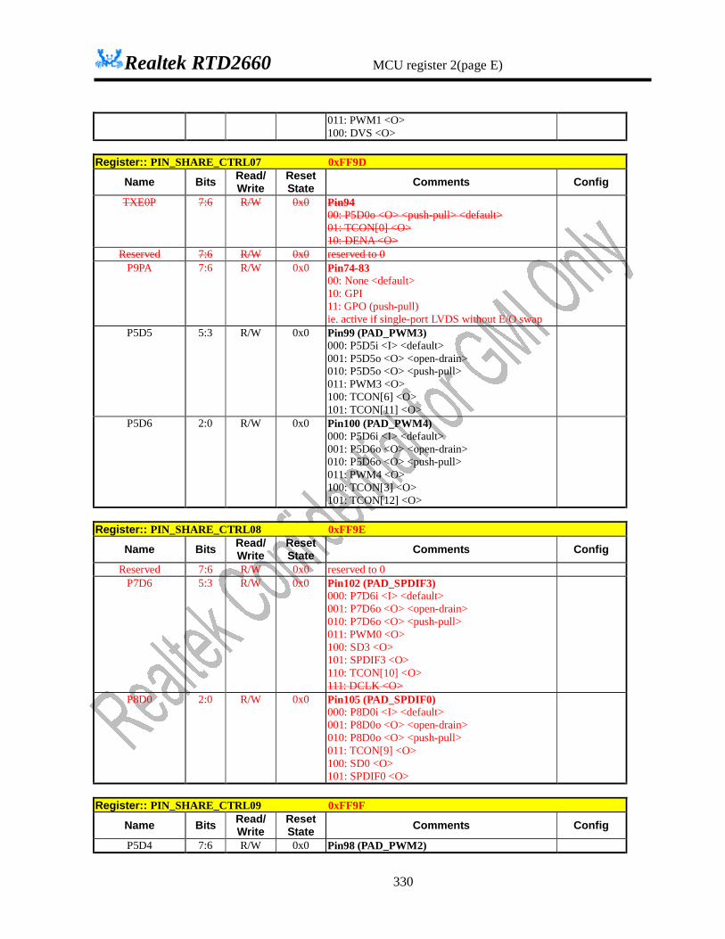
Realtek RTD2660 MCU register 2(page E)
330
011: PWM1 <O> 100: DVS <O>
Register:: PIN_SHARE_CTRL07 0xFF9D
Name Bits Read/ Write
Reset State Comments Config
TXE0P 7:6 R/W 0x0 Pin94 00: P5D0o <O> <push-pull> <default> 01: TCON[0] <O> 10: DENA <O>
Reserved 7:6 R/W 0x0 reserved to 0 P9PA 7:6 R/W 0x0 Pin74-83
00: None <default> 10: GPI 11: GPO (push-pull) ie. active if single-port LVDS without E/O swap
P5D5 5:3 R/W 0x0 Pin99 (PAD_PWM3) 000: P5D5i <I> <default> 001: P5D5o <O> <open-drain> 010: P5D5o <O> <push-pull> 011: PWM3 <O> 100: TCON[6] <O> 101: TCON[11] <O>
P5D6 2:0 R/W 0x0 Pin100 (PAD_PWM4) 000: P5D6i <I> <default> 001: P5D6o <O> <open-drain> 010: P5D6o <O> <push-pull> 011: PWM4 <O> 100: TCON[3] <O> 101: TCON[12] <O>
Register:: PIN_SHARE_CTRL08 0xFF9E
Name Bits Read/ Write
Reset State Comments Config
Reserved 7:6 R/W 0x0 reserved to 0 P7D6 5:3 R/W 0x0 Pin102 (PAD_SPDIF3)
000: P7D6i <I> <default> 001: P7D6o <O> <open-drain> 010: P7D6o <O> <push-pull> 011: PWM0 <O> 100: SD3 <O> 101: SPDIF3 <O> 110: TCON[10] <O> 111: DCLK <O>
P8D0 2:0 R/W 0x0 Pin105 (PAD_SPDIF0) 000: P8D0i <I> <default> 001: P8D0o <O> <open-drain> 010: P8D0o <O> <push-pull> 011: TCON[9] <O> 100: SD0 <O> 101: SPDIF0 <O>
Register:: PIN_SHARE_CTRL09 0xFF9F
Name Bits Read/ Write
Reset State Comments Config
P5D4 7:6 R/W 0x0 Pin98 (PAD_PWM2)

Realtek RTD2660 MCU register 2(page E)
331
00: P5D4i <I> <default> 01: P5D4o <O> <open-drain> 10: P5D4o <O> <push-pull> 11: PWM2 <O>
P5D7 5:3 R/W 0x0 Pin101 (PAD_PWM5) 000: P5D7i <I> <default> 001: P5D7o <O> <open-drain> 010: P5D7o <O> <push-pull> 011: PWM5 <O> 100: TCON[0] <O>
P8D1 2:0 R/W 0x0 Pin108 (PAD_MCK) 000: P8D1i <I> <default> 001: P8D1o <O> <open-drain> 010: P8D1o <O> <push-pull> 011: CLKO <O> 100: MCK <O> 101: TCON[7] <O>
Register:: PIN_SHARE_CTRL0A 0xFFA0
Name Bits Read/ Write
Reset State Comments Config
Reserved 7 R/W 0 reserved to 0 P7D5 6:4 R/W 0x0 Pin103 (PAD_SPDIF2)
000: P7D5i <I> <default> 001: P7D5o <O> <open-drain> 010: P7D5o <O> <push-pull> 011: PWM1 <O> 100: SD2 <O> 101: SPDIF2 <O> 110: TCON[8] <O> 111: IICSCL <IO> <open-drain>
P7D4 3:1 R/W 0x0 Pin104 (PAD_SPDIF1) 000: P7D4i <I> <default> 001: P7D4o <O> <open-drain> 010: P7D4o <O> <push-pull> 011: SD1 <O> 100: IRQ <O> 101: TCON[5] <O> 110: SPDIF1 <O> 111: IICSDA <IO> <open-drain>
Reserved 0 R/W 0 reserved to 0 Register:: PIN_SHARE_CTRL0B 0xFFA1
Name Bits Read/ Write
Reset State Comments Config
Reserved 7 R/W 0 reserved to 0 P3D2 6:4 R/W 0x0 Pin109 (PAD_SCK)
000: P3D2i <I> <default> 001: P3D2o <O> <open-drain> 010: P3D2o <O> <push-pull> 011: INT0 <I> 100: TCON[3] <O> 101: SCK <O>
Reserved 3 R/W 0 reserved to 0 P3D3 2:0 R/W 0x0 Pin110 (PAD_WS)
000: P3D3i <I> <default>

Realtek RTD2660 MCU register 2(page E)
332
001: P3D3o <O> <open-drain> 010: P3D3o <O> <push-pull> 011: INT1 <I> 100: TCON[6] <O> 101: WS <O>
Register:: PIN_SHARE_CTRL0C 0xFFA2
Name Bits Read/ Write
Reset State Comments Config
Reserved 7 R/W 0 reserved to 0 P3D4 6:4 R/W 0x0 Pin111 (PAD_SD0)
000: P3D4i <I> <default> 001: P3D4o <O> <open-drain> 010: P3D4o <O> <push-pull> 011: T0 <I> 100: TCON[4] <O> 101: SD0 <O> 110: SPDIF0 <O>
Reserved 3 R/W 0 reserved to 0 P3D5 2:0 R/W 0x0 Pin112 (PAD_SD1)
000: P3D5i <I> <default> 001: P3D5o <O> <open-drain> 010: P3D5o <O> <push-pull> 011: T1 <I> 100: TCON[9] <O> 101: SD1 <O> 110: SPDIF1 <O>
Register:: PIN_SHARE_CTRL0D 0xFFA3
Name Bits Read/ Write
Reset State Comments Config
Reserved 7 R/W 0 reserved to 0 P3D6 6:4 R/W 0x0 Pin113 (PAD_SD2)
000: P3D6i <I> <default> 001: P3D6o <O> <open-drain> 010: P3D6o <O> <push-pull> 011: TCON[1] <O> 100: SD2 <O> 101: SPDIF2 <O> 110: IrDA <I>
Reserved 3 R/W 0 reserved to 0 P3D7 2:0 R/W 0x0 Pin114 (PAD_SD3)
000: P3D7i <I> <default> 001: P3D7o <O> <open-drain> 010: P3D7o <O> <push-pull> 011: TCON[13] <O> 100: SD3 <O> 101: SPDIF3 <O> 110: VCLK <I>
Register:: PIN_SHARE_CTRL0E 0xFFA4
Name Bits Read/ Write
Reset State Comments Config
DDCSCL2 7:6 R/W 0x0 Pin124 (PAD_DDCSCL2) 00: DDCSCL2 <IO> <default> 01: P7D0i <I>
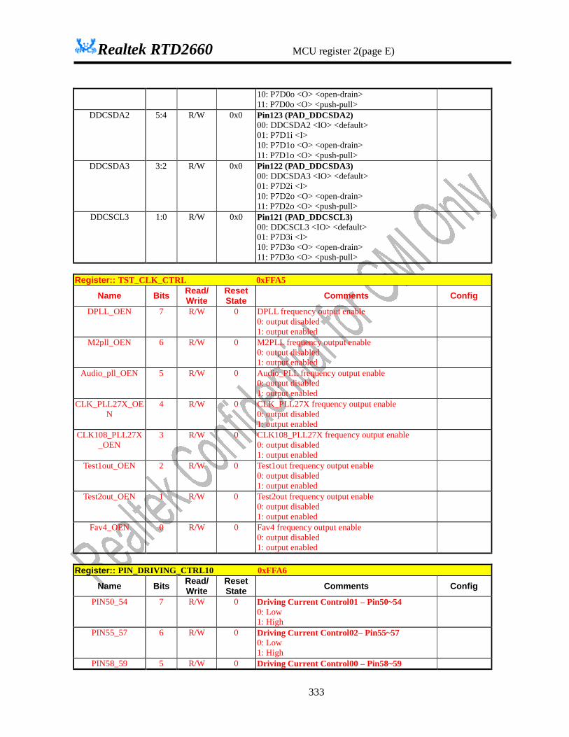
Realtek RTD2660 MCU register 2(page E)
333
10: P7D0o <O> <open-drain> 11: P7D0o <O> <push-pull>
DDCSDA2 5:4 R/W 0x0 Pin123 (PAD_DDCSDA2) 00: DDCSDA2 <IO> <default> 01: P7D1i <I> 10: P7D1o <O> <open-drain> 11: P7D1o <O> <push-pull>
DDCSDA3 3:2 R/W 0x0 Pin122 (PAD_DDCSDA3) 00: DDCSDA3 <IO> <default> 01: P7D2i <I> 10: P7D2o <O> <open-drain> 11: P7D2o <O> <push-pull>
DDCSCL3 1:0 R/W 0x0 Pin121 (PAD_DDCSCL3) 00: DDCSCL3 <IO> <default> 01: P7D3i <I> 10: P7D3o <O> <open-drain> 11: P7D3o <O> <push-pull>
Register:: TST_CLK_CTRL 0xFFA5
Name Bits Read/ Write
Reset State Comments Config
DPLL_OEN 7 R/W 0 DPLL frequency output enable 0: output disabled 1: output enabled
M2pll_OEN 6 R/W 0 M2PLL frequency output enable 0: output disabled 1: output enabled
Audio_pll_OEN 5 R/W 0 Audio_PLL frequency output enable 0: output disabled 1: output enabled
CLK_PLL27X_OEN
4 R/W 0 CLK_PLL27X frequency output enable 0: output disabled 1: output enabled
CLK108_PLL27X_OEN
3 R/W 0 CLK108_PLL27X frequency output enable 0: output disabled 1: output enabled
Test1out_OEN 2 R/W 0 Test1out frequency output enable 0: output disabled 1: output enabled
Test2out_OEN 1 R/W 0 Test2out frequency output enable 0: output disabled 1: output enabled
Fav4_OEN 0 R/W 0 Fav4 frequency output enable 0: output disabled 1: output enabled
Register:: PIN_DRIVING_CTRL10 0xFFA6
Name Bits Read/ Write
Reset State Comments Config
PIN50_54 7 R/W 0 Driving Current Control01 – Pin50~54 0: Low 1: High
PIN55_57 6 R/W 0 Driving Current Control02– Pin55~57 0: Low 1: High
PIN58_59 5 R/W 0 Driving Current Control00 – Pin58~59
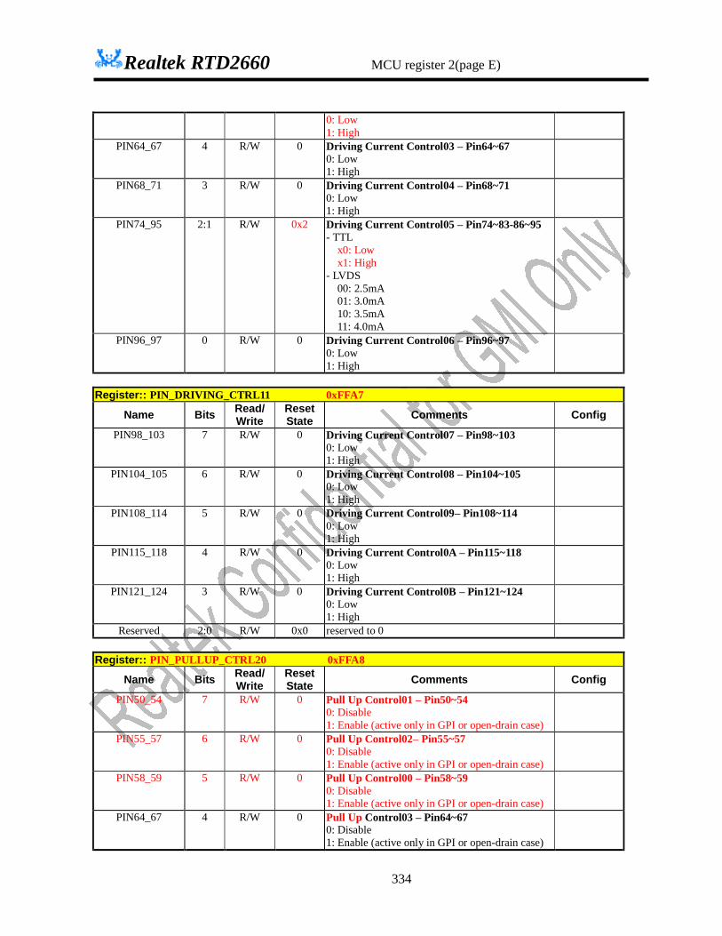
Realtek RTD2660 MCU register 2(page E)
334
0: Low 1: High
PIN64_67 4 R/W 0 Driving Current Control03 – Pin64~67 0: Low 1: High
PIN68_71 3 R/W 0 Driving Current Control04 – Pin68~71 0: Low 1: High
PIN74_95 2:1 R/W 0x2 Driving Current Control05 – Pin74~83-86~95 - TTL
x0: Low x1: High
- LVDS 00: 2.5mA 01: 3.0mA 10: 3.5mA 11: 4.0mA
PIN96_97 0 R/W 0 Driving Current Control06 – Pin96~97 0: Low 1: High
Register:: PIN_DRIVING_CTRL11 0xFFA7
Name Bits Read/ Write
Reset State Comments Config
PIN98_103 7 R/W 0 Driving Current Control07 – Pin98~103 0: Low 1: High
PIN104_105 6 R/W 0 Driving Current Control08 – Pin104~105 0: Low 1: High
PIN108_114 5 R/W 0 Driving Current Control09– Pin108~114 0: Low 1: High
PIN115_118 4 R/W 0 Driving Current Control0A – Pin115~118 0: Low 1: High
PIN121_124 3 R/W 0 Driving Current Control0B – Pin121~124 0: Low 1: High
Reserved 2:0 R/W 0x0 reserved to 0 Register:: PIN_PULLUP_CTRL20 0xFFA8
Name Bits Read/ Write
Reset State Comments Config
PIN50_54 7 R/W 0 Pull Up Control01 – Pin50~54 0: Disable 1: Enable (active only in GPI or open-drain case)
PIN55_57 6 R/W 0 Pull Up Control02– Pin55~57 0: Disable 1: Enable (active only in GPI or open-drain case)
PIN58_59 5 R/W 0 Pull Up Control00 – Pin58~59 0: Disable 1: Enable (active only in GPI or open-drain case)
PIN64_67 4 R/W 0 Pull Up Control03 – Pin64~67 0: Disable 1: Enable (active only in GPI or open-drain case)

Realtek RTD2660 MCU register 2(page E)
335
PIN68_71 3 R/W 0 Pull Up Control04 – Pin68~71 0: Disable 1: Enable (active only in GPI or open-drain case)
Reserved 2:1 R/W 0 reserved to 0 PIN96_97 0 R/W 0 Pull Up Control06 – Pin96~97
0: Disable 1: Enable (active only in GPI or open-drain case)
Register:: PIN_PULLUP_CTRL21 0xFFA9
Name Bits Read/ Write
Reset State Comments Config
PIN98_103 7 R/W 0 Pull Up Control07 – Pin98~103 0: Disable 1: Enable (active only in GPI or open-drain case)
PIN104_105 6 R/W 0 Pull Up Control08 – Pin104~105 0: Disable 1: Enable (active only in GPI or open-drain case)
PIN108_114 5 R/W 0 Pull Up Control09– Pin108~114 0: Disable 1: Enable (active only in GPI or open-drain case)
Reserved 4 R/W 0x0 reserved to 0 PIN121_124 3 R/W 0 Pull Up Control0B – Pin121~124
0: Disable 1: Enable (active only in GPI or open-drain case)
Reserved 2 R/W 0x0 reserved to 0 XCLK_OEN 1 R/W 0 XCLK frequency output enable
0: output disabled 1: output enabled
CKT_PLL27X_OEN
0 R/W 0 CKT_PLL27X frequency output enable 0: output disabled 1: output enabled
CEC function
CEC Control Register In CEC function, write_reg pulses should have distances larger than 3 XTAL clk period at least. Register:: cec_cr_1 0xFFAA
Name Bits R/W Default Comments Config Reserved 7:5 -- -- ini_adr_sel
4 R/W 0 1:initial address change 0:use original address
ini_adr
3:0 R/W 0x1 Initial address when ini_adr_sel = 1
Register::cec_cr0 0xFFAB
Name Bits R/W Default Comments Config cec_mode 7:6 R/W 0x0 00: Disable CEC module
01: Enable CEC Normal Operation 10: PAD Output Test Mode.

Realtek RTD2660 MCU register 2(page E)
336
11: Digital Loopback, Tx Data will be loopback before PAD. Note. 1. As CEC module is disabled, RX will not ACK any transaction which destination address is the same with CECLOCADDR or 0xf.
test_mode_pad_data 5 R/W 0x1 0: CEC PAD output low
1: CEC PAD output high
test_mode_pad_en 4 R/W 0x0 0: output high impedance 1:PAD output enable This bit is active with CEC_Mode=10 only.
logical_addr 3:0 R/W 0xF CEC device logical (local) address Register::cec_cr1 0xFFAC
Name Bits R/W Default Comments Config timer_div 7:0 R/W 0x14 DAC ENP(Enable Pulse) divides into Timer Enable Pulse.
And Timer Enable Pulse is equal to Input Sample Enable Pulse. Its default value is 0.8MHz divides into 20 to 40KHz(25us).。 CEC clock frequency is used for the bit timers in the receiver and transmitter modes.
Register::cec_cr2 0xFFAD
Name Bits R/W Default Comments Config pre_div 7:0 R/W 0x21 Divisor for CEC DAC Clock
BusCLK CECDiv CK_CEC 162MHz 202 0.8019MHz 27MHz 33 0.8182MHz
Register::cec_cr3 0xFFAE
Name Bits R/W Default Comments Config unreg_ack_en 7 R/W 0x0 If rx logical addr = 0xF, when receiving a broadcast
signal (destination addr = 0xF) 1 : response ack 2 : non to response ack
pad_s_ctrl 6:5 R/W 0x1 CEC PAD Current Control of Charge Pump 00: 0.75 uA 01: 1 uA 10: 1.25 uA 11: 1.5 uA
pad_delay 4:0 R/W 0x03 The delay from CEC PAD going high to being disable. Delay: (1+CECPADDELAY)*25us Typical Value: 01~03 (50us~100us) For Normal Mode only.
Register::cec_rt0 0xFFAF
Name Bits R/W Default Comments Config cec_rt0_rsv 7:6 R/W 0x0 Reserved Register wt_cnt 5:0 R - Retry Wait Time Register::cec_rt1 0xFFB0

Realtek RTD2660 MCU register 2(page E)
337
Name Bits R/W Default Comments Config cec_rt1_rsv 7:5 R/W 0x0 lattest 4 R - 1: The last initiator own CEC bus is this device retry_no 3:0 R/W 0x5 Maximum re-transmission times for a single frame, when
device is a initiator and device detect low impedance error. In continue mode, retry is inactive.
Register::cec_rx0 0xFFB1
Name Bits R/W Default Comments Config rx_en 7 R - Write 1 to enable Rx
As CEC_enable=1 and CECRxEn=0, RX will ACK the transaction which destination address is the same with CECLOCADDR or 0xf
wclr_out
rx_rst 6 R/W 0x0 Write 1 to reset Rx State and its FIFO status After finishing each transaction, software should reset Rx part to clear CECRxEOM, CECRxINT and CECRxFIFOov status bits.
rx_continuous 5 R/W 0x0 0/1:Normal mode / Continuous mode In continuous mode, RxINT will be set to 1 when Rx receive new 8 bytes or EOM. In normal mode, RxINT will be set to 1 iff Rx receive EOM.
rx_int_en 4 R/W 0x0 1 : CEC Rx interrupt enable If enabled, hardware will trigger interrupt per 8 bytes received or EOM
init_addr 3:0 R - The latest Initiator Address (when device is a follower) Register::cec_rx1 0xFFB2
Name Bits R/W Default Comments Config rx_eom 7 R - When EOM is received, RxEn will be reset to 0 and
RxINT will be set to 1.
rx_int 6 R - 1 : CEC Rx interrupt pending (write 1 to clear) wclr_out rx_fifo_ov 5 R - 1 : Overflow status for CEC 16-byte FIFO rx_fifo_cnt 4:0 R - The number of byte has been received by Rx Register::cec_tx0 0xFFB3
Name Bits R/W Default Comments Config tx_en 7 R - Write 1 to enable Tx transmission
Tx will detect signal free time, and then transmission and re-try automatically.
wclr_out
tx_rst 6 R/W 0x0 Write 1 to reset Tx State and its FIFO status
After finishing each transaction, software should reset Tx part to clear CECTxEOM, CECTxINT and CECTxFIFOud status bits.
tx_continuous 5 R/W 0x0 Tx continuous mode 0: Normal mode
1: Continuous mode, software should clear this bit as the last byte is written into Tx FIFO to indicate the end of transmitting data.

Realtek RTD2660 MCU register 2(page E)
338
tx_int_en 4 R/W 0x0 1 : CEC Tx interrupt enable
If enabled, hardware will trigger interrupt per 8 bytes transmitted or EOM
dest_addr 3:0 R/W 0x0 Destination Address (when device is a initiator) Register::cec_tx1 0xFFB4
Name Bits R/W Default Comments Config tx_eom 7 R - The transmission has ended. tx_int 6 R - 1 : CEC Tx interrupt pending (write 1 to clear) wclr_ou
t tx_fifo_ud 5 R - 1 : Underflow status for CEC 16-byte Tx FIFO tx_fifo_cnt 4:0 R - The number of byte will been transmitted by Tx
Note : following table illustrates the status with the combination of CECTxEn, CECTxEOM, CECTxINT and CECTxContinue after transmitting.
CECTxEn CECTxEOM CECTxINT CECTxContinue Complete transmission incorrectly and not in Continue Mode
0 0 1 0
Complete transmission correctly and not in Continue Mode
0 1 1 0
Complete transmission incorrectly and in Continue Mode
0 0 1 0
Transmitted 8 bytes correctly and still in Continue Mode, software should push data into Tx fifo as necessary
1 0 1 1
Complete transmission and in Continue Mode
0 1 1 0 (because software clear to 0 after pushing remaining datum into TX fifo)
TX fifo is underflow (in continue mode only) Note : this is the same with CECTxFIFOud=1
0 0 1 1
Register::cec_tx_fifo 0xFFB5
Name Bits R/W Default Comments Config tx_dat 7:0 R/W - Tx FIFO data output port rport
wport Register::cec_rx_fifo 0xFFB6
Name Bits R/W Default Comments Config rx_dat 7:0 R/W - Rx FIFO data input port rport
wport

Realtek RTD2660 MCU register 3 (Page F)
339
Register::cec_rx_start0 0xFFB7
Name Bits R/W Default Comments Config rx_start_low 7:0 R/W 0x8C Minimum width (3.5ms) Register::cec_rx_start1 0xFFB8
Name Bits R/W Default Comments Config rx_start_period 7:0 R/W 0xBC Maximum width (4.7ms) Register::cec_rx_data0 0xFFB9
Name Bits R/W Default Comments Config rx_data_sample 7:0 R/W 0x2A Sample Time (1.05ms) Register::cec_rx_data1 0xFFBA
Name Bits R/W Default Comments Config rx_data_period 7:0 R/W 0x52, Minimum data bit width (2.05ms) Register::cec_tx_start0 0xFFBB
Name Bits R/W Default Comments Config tx_start_low 7:0 R/W 0x94 3.7ms (0.025*148) Register::cec_tx_start1 0xFFBC
Name Bits R/W Default Comments Config tx_start_high 7:0 R/W 0x20 0.8ms (4.5ms – 3.7ms) Register::cec_tx_data0 0xFFBD
Name Bits R/W Default Comments Config tx_data_low 7:0 R/W 0x18 0.6ms Register::cec_tx_data1 0xFFBE
Name Bits R/W Default Comments Config tx_data_01 7:0 R/W 0x24 0.9ms Register::cec_tx_data2 0xFFBF
Name Bits R/W Default Comments Config tx_data_high 7:0 R/W 0x24 0.9ms

Realtek RTD2660 MCU register 3 (Page F)
340
MCU register 3 (Page F)
GPIO Control
Register::Port_read_control 0xFFC0
Name Bits R/W Default Comments Config
PA_pin_reg_n 7 R/W 0 Source selection for PA read back
0: register
1: bus value
P9_pin_reg_n 6 R/W 0 Source selection for P9 read back
0: register
1: bus value
P8_pin_reg_n 5 R/W 0 Source selection for P8 read back
0: register
1: bus value
P7_pin_reg_n 4 R/W 0 Source selection for P7 read back
0: register
1: bus value
P6_pin_reg_n 3 R/W 0 Source selection for P6 read back
0: register
1: bus value
P5_pin_reg_n 2 R/W 0 Source selection for P5 read back
0: register
1: bus value
P3_pin_reg_n 1 R/W 0 Source selection for P3 read back*
0: register
1: bus value
P1_pin_reg_n 0 R/W 0 Source selection for P1 read back*
0: register
1: bus value
*: only effect in external MCU control, embedded MCU will control the source by assembly code. Register::Port52_pin_reg 0xFFC1
Name Bits R/W Default Comments Config
Reserved 7:1 -- 0 Reserved

Realtek RTD2660 MCU register 3 (Page F)
341
P52 0 R/W 1 Input/output value of P5.2 Rport wport
Register::Port53_pin_reg 0xFFC2
Name Bits R/W Default Comments Config
Reserved 7:1 -- 0 Reserved
P53 0 R/W 1 Input/output value of P5.3 Rport wport
Register::Port54_pin_reg 0xFFC3
Name Bits R/W Default Comments Config
Reserved 7:1 -- 0 Reserved
P54 0 R/W 1 Input/output value of P5.4 Rport wport
Register::Port55_pin_reg 0xFFC4
Name Bits R/W Default Comments Config
Reserved 7:1 -- 0 Reserved
P55 0 R/W 1 Input/output value of P5.5 Rport wport
Register::Port56_pin_reg 0xFFC5
Name Bits R/W Default Comments Config
Reserved 7:1 -- 0 Reserved
P56 0 R/W 1 Input/output value of P5.6 Rport wport

Realtek RTD2660 MCU register 3 (Page F)
342
Register::Port57_pin_reg 0xFFC6
Name Bits R/W Default Comments Config
Reserved 7:1 -- 0 Reserved
P57 0 R/W 1 Input/output value of P5.7 Rport wport
Register::Port60_pin_reg 0xFFC7
Name Bits R/W Default Comments Config
Reserved 7:1 -- 0 Reserved
P60 0 R/W 1 Input/output value of P6.0 Rport wport
Register::Port61_pin_reg 0xFFC8
Name Bits R/W Default Comments Config
Reserved 7:1 -- 0 Reserved
P61 0 R/W 1 Input/output value of P6.1 Rport wport
Register::Port62_pin_reg 0xFFC9
Name Bits R/W Default Comments Config
Reserved 7:1 -- 0 Reserved
P62 0 R/W 1 Input/output value of P6.2 Rport wport
Register::Port63_pin_reg 0xFFCA
Name Bits R/W Default Comments Config

Realtek RTD2660 MCU register 3 (Page F)
343
Reserved 7:1 -- 0 Reserved
P63 0 R/W 1 Input/output value of P6.3 Rport wport
Register::Port64_pin_reg 0xFFCB
Name Bits R/W Default Comments Config
Reserved 7:1 -- 0 Reserved
P64 0 R/W 1 Input/output value of P6.4 Rport wport
Register::Port65_pin_reg 0xFFCC
Name Bits R/W Default Comments Config
Reserved 7:1 -- 0 Reserved
P65 0 R/W 1 Input/output value of P6.5 Rport wport
Register::Port66_pin_reg 0xFFCD
Name Bits R/W Default Comments Config
Reserved 7:1 -- 0 Reserved
P66 0 R/W 1 Input/output value of P6.6 Rport wport
Register::Port67_pin_reg 0xFFCE
Name Bits R/W Default Comments Config
Reserved 7:1 -- 0 Reserved
P67 0 R/W 1 Input/output value of P6.7 Rport wport

Realtek RTD2660 MCU register 3 (Page F)
344
Register::Port70_pin_reg 0xFFCF
Name Bits R/W Default Comments Config
Reserved 7:1 -- 0 Reserved
P70 0 R/W 1 Input/output value of P7.0 Rport wport
Register::Port71_pin_reg 0Xffd0
Name Bits R/W Default Comments Config
Reserved 7:1 -- 0 Reserved
P71 0 R/W 1 Input/output value of P7.1 Rport wport
Register::Port72_pin_reg 0xFFD1
Name Bits R/W Default Comments Config
Reserved 7:1 -- 0 Reserved
P72 0 R/W 1 Input/output value of P7.2 Rport wport
Register::Port73_pin_reg 0xFFD2
Name Bits R/W Default Comments Config
Reserved 7:1 -- 0 Reserved
P73 0 R/W 1 Input/output value of P7.3 Rport wport
Register::Port74_pin_reg 0xFFD3
Name Bits R/W Default Comments Config

Realtek RTD2660 MCU register 3 (Page F)
345
Reserved 7:1 -- 0 Reserved
P74 0 R/W 1 Input/output value of P7.4 Rport wport
Register::Port75_pin_reg 0xFFD4
Name Bits R/W Default Comments Config
Reserved 7:1 -- 0 Reserved
P75 0 R/W 1 Input/output value of P7.5 Rport wport
Register::Port76_pin_reg 0xFFD5
Name Bits R/W Default Comments Config
Reserved 7:1 -- 0 Reserved
P76 0 R/W 1 Input/output value of P7.6 Rport wport
Register::Port80_pin_reg 0xFFD6
Name Bits R/W Default Comments Config
Reserved 7:1 -- 0 Reserved
P80 0 R/W 1 Input/output value of P8.0 Rport wport
Register::Port81_pin_reg 0xFFD7
Name Bits R/W Default Comments Config
Reserved 7:1 -- 0 Reserved
P81 0 R/W 1 Input/output value of P8.1 Rport wport

Realtek RTD2660 MCU register 3 (Page F)
346
Register::Port90_pin_reg 0xFFD8
Name Bits R/W Default Comments Config
Reserved 7:1 -- 0 Reserved
P90 0 R/W 1 Input/output value of P9.0 Rport wport
Register::Port91_pin_reg 0xFFD9
Name Bits R/W Default Comments Config
Reserved 7:1 -- 0 Reserved
P91 0 R/W 1 Input/output value of P9.1 Rport wport
Register::Port92_pin_reg 0xFFDA
Name Bits R/W Default Comments Config
Reserved 7:1 -- 0 Reserved
P92 0 R/W 1 Input/output value of P9.2 Rport wport
Register::Port93_pin_reg 0xFFDB
Name Bits R/W Default Comments Config
Reserved 7:1 -- 0 Reserved
P93 0 R/W 1 Input/output value of P9.3 Rport wport
Register::Port94_pin_reg 0xFFDC
Name Bits R/W Default Comments Config
Reserved 7:1 -- 0 Reserved

Realtek RTD2660 MCU register 3 (Page F)
347
P94 0 R/W 1 Input/output value of P9.4 Rport wport
Register::Porta0_pin_reg 0xFFDD
Name Bits R/W Default Comments Config
Reserved 7:1 -- 0 Reserved
PA0 0 R/W 1 Input/output value of PA.0 Rport wport
Register::Porta1_pin_reg 0xFFDE
Name Bits R/W Default Comments Config
Reserved 7:1 -- 0 Reserved
PA1 0 R/W 1 Input/output value of PA.1 Rport wport
Register::Porta2_pin_reg 0xFFDF
Name Bits R/W Default Comments Config
Reserved 7:1 -- 0 Reserved
PA2 0 R/W 1 Input/output value of PA.2 Rport wport
Register::Porta3_pin_reg 0xFFE0
Name Bits R/W Default Comments Config
Reserved 7:1 -- 0 Reserved
PA3 0 R/W 1 Input/output value of PA.3 Rport wport
Register::Porta4_pin_reg 0xFFE1
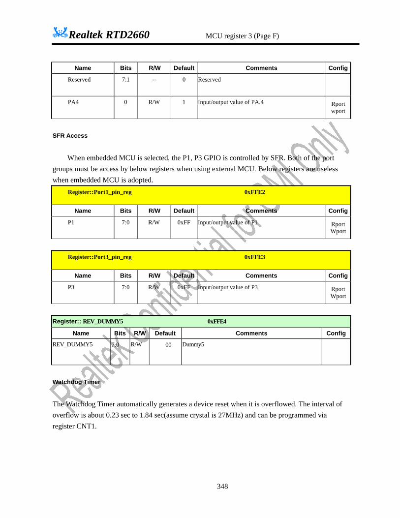
Realtek RTD2660 MCU register 3 (Page F)
348
Name Bits R/W Default Comments Config
Reserved 7:1 -- 0 Reserved
PA4 0 R/W 1 Input/output value of PA.4 Rport wport
SFR Access
When embedded MCU is selected, the P1, P3 GPIO is controlled by SFR. Both of the port groups must be access by below registers when using external MCU. Below registers are useless when embedded MCU is adopted.
Register::Port1_pin_reg 0xFFE2
Name Bits R/W Default Comments Config
P1 7:0 R/W 0xFF Input/output value of P1 Rport Wport
Register::Port3_pin_reg 0xFFE3
Name Bits R/W Default Comments Config
P3 7:0 R/W 0xFF Input/output value of P3 Rport Wport
Register:: REV_DUMMY5 0xFFE4
Name Bits R/W Default Comments Config
REV_DUMMY5 7:0 R/W 00 Dummy5
Watchdog Timer
The Watchdog Timer automatically generates a device reset when it is overflowed. The interval of overflow is about 0.23 sec to 1.84 sec(assume crystal is 27MHz) and can be programmed via register CNT1.
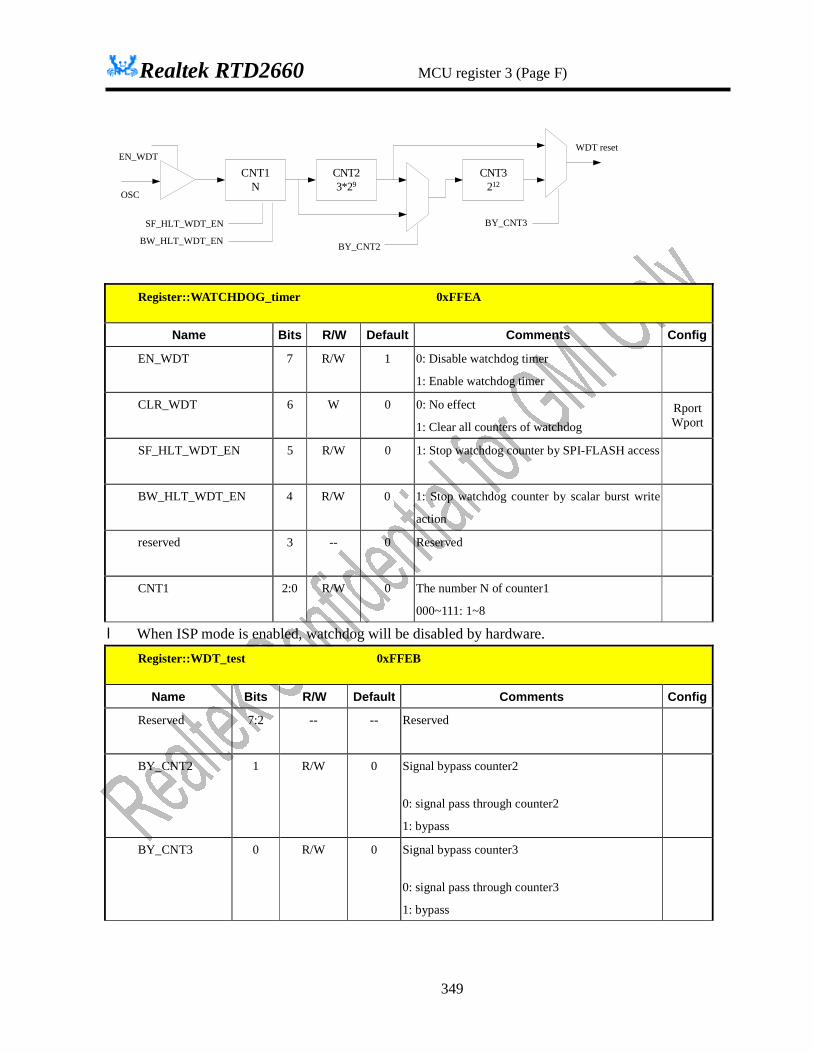
Realtek RTD2660 MCU register 3 (Page F)
349
CNT23*29
CNT1N
CNT3212
EN_WDT
BY_CNT2
BY_CNT3
WDT reset
OSC
SF_HLT_WDT_EN
BW_HLT_WDT_EN
Register::WATCHDOG_timer 0xFFEA
Name Bits R/W Default Comments Config
EN_WDT 7 R/W 1 0: Disable watchdog timer
1: Enable watchdog timer
CLR_WDT 6 W 0 0: No effect
1: Clear all counters of watchdog Rport Wport
SF_HLT_WDT_EN 5 R/W 0 1: Stop watchdog counter by SPI-FLASH access
BW_HLT_WDT_EN 4 R/W 0 1: Stop watchdog counter by scalar burst write
action
reserved 3 -- 0 Reserved
CNT1 2:0 R/W 0 The number N of counter1
000~111: 1~8
l When ISP mode is enabled, watchdog will be disabled by hardware. Register::WDT_test 0xFFEB
Name Bits R/W Default Comments Config
Reserved 7:2 -- -- Reserved
BY_CNT2 1 R/W 0 Signal bypass counter2
0: signal pass through counter2
1: bypass
BY_CNT3 0 R/W 0 Signal bypass counter3
0: signal pass through counter3
1: bypass

Realtek RTD2660 MCU register 3 (Page F)
350
In System Programming
User can program the external serial FLASH by internal hardware without removing serial FLASH from the system. RTD2662 utilizes DDC channel (ADC/DDC2/DDC3) to communicate with IIC host for ISP function. The ISP protocol is mainly compatible with DDC protocol. However, one significant difference is that the LSB of 7-bit ISP address is the address auto increase bit. Thus, we can improve the flash program speed.
Register::ISP_slave_address 0xFFEC
Name Bits R/W Default Comments Config
ISP_ADDR 7:2 R/W 25 ISP slave address
ISP_ADDR_INC_A 1 R 0 Received LSB of ISP slave address of ADC
DDC channel
0: address is nonincrease
1: address is auto-increase
ISP_ADDR_INC_D 0 R 0 Received LSB of ISP slave address of
DDC2 channel
0: address is nonincrease
1: address is auto-increase
Register::MCU_control 0xFFED
Name Bits R/W Default Comments Config
PORT_PIN_REG 7 R/W 1 port_pin_reg_n enable
0: port_pin_reg_n signal is disabled
1: port_pin_reg_n signal is enabled
ISP_ADDR_INC_H 6 R 0 Received LSB of ISP slave address of
DDC3 channel
0: address is nonincrease
1: address is auto-increase
FLASH_CLK_DIV
5:2
R/W 2 SPI-FLASH clock divider, its clock source
is selected by MCU_CLK_SEL, default is
MCU_CLK_SEL/2

Realtek RTD2660 MCU register 3 (Page F)
351
MCU_CLK_SEL 1 R/W 0 CPU clock source select
0: CPU clock is from Crystal divided by
DIV
1: CPU clock is from PLL divided by DIV
CKOUT_SEL 0 R/W 0 CLKO1 & CLKO2 select
0: Select Crystal output
1: Select Mcu clk output
Register::MCU_clock_control 0xFFEE
Name Bits R/W Default Comments Config
Reserved 7 -- -- Rerserved
MCU_PERI_NON_STOP 6 R/W 0 1: keep mcu peripheral running whiel mcu
stopped by spi flash access
0: peripheral will be stopped with mcu*.
MCU_CLK_DIV 5:2 R/W 1 MCU clock is FLASH
clock/MCU_CLK_DIV.
SOF_RST 1 R/W 0 Software reset mcu
0: No effect
1: reset RTD2662
Rport Wport
SCA_HRST 0 R/W 0 Hardware reset for Scalar
0: No effect
1: reset SCALAR module
*note: this register bit[6] only has effect on peripheral built in SFR, which are timer 0, 1, 2 and serial port 1. Register::RAM_test 0xFFEF
Name Bits R/W Default Comments Config
reserved 7:5 -- 0 Reserved
Test_mode 4 R/W 0 When test_mode of scalar is enabled for
embedded mcu output, the bus is decided by
following settins.
0: adca_out[5:0], adca_out_valid,
adca_ckini, adcb_out[9:0], adcb_out_valid,
Realtek RTD2660 MCU register 3 (Page F)
352
adcb_ckini, flash_mcu_gated, bist_clk,
xram_clk, adc_div270_clk, adc_div9_clk ,
eclk_ng , eclk_n , eclk , shift_in_clk, fclk
1: 13’b0, st_cmd [2:0], st_ph [3:0],
find_d01_value, find_d01, find_rpt,, find_str,
st_data, st_lead, st_search, rmtin, remote_in2, irin
EXT_RAM_BIST 3 R/W 0 Start BIST function for MCU external RAM
(1024 bytes)
0: finished and clear
1: start
Rport Wport
EXT_RAM_STA 2 R 0 Test result about MCU external RAM
0: fail
1: ok
INT_RAM_BIST 1 R/W 0 Start BIST function for MCU internal RAM
(256 bytes)
0: finished and clear
1: start
Rport Wport
INT_RAM_STA 0 R 0 Test result about MCU internal RAM
0: fail
1: ok
Register:: REV_DUMMY6 0xFFF2
Name Bits R/W Default Comments Config
REV_DUMMY6 7:0 R/W 00 Dummy6
Scalar Interface
Scalar Interface Related Register External host interface is selected by power-on latch. The internal XFR access will be auto-switched to external host interface by power-on latch, too. Scalar’s register map must reserve addresses for mapping necessary XFR when using external host interface.

Realtek RTD2660 MCU register 3 (Page F)
353
Register:: SCA_INF_CONTROL 0xFFF3
Name Bits R/W Default Comments Config
REG_READ_EN 7 R 0 Enable Read Action of Scalar Interface
REG_WRITE_EN 6 R 0 Enable Write Action of Scalar Interface
ADDR_NON_INC 5 R/W 0 1: turn-off address auto inc
REG_BURCMD_WR 4 R/W 0 Enable burst write function, mcu will halt till action done or an interrupt triggered. *
Rport
Wport
REG_BURDAT_WR 3 R/W 0 Enable burst write data to HOST_ADDR, mcu will halt till action done or an interrupt triggered *
Rport
Wport
BURST_CMD_ERR 2 R 0 Burst write command error, value of SCA_INF_BWR_COUNT mismatch the length in content
DIS_INT_RLS 1 R/W 0 1: disable the function of releasing mcu by interrupt
PAGE_ADDR_MAP 0 R/W 0 0: Using normal XFR address to access all XFR
1: Using external page address for XFR. XFR can only be
accessed by SCA_INF_ADDR, SCA_INF_DATA
*: MCU will be released when interrupt is triggered. The bit value will maintain 1 before the operation is done. Rewriting this bit to 1 to continue the burst cmd/data write mode. Register:: SCA_INF_ADDR 0xFFF4
Name Bits R/W Default Comments Config
HOST_ADDR 7:0 R/W 0x00 Host Interface Access Address Rport
Wport
Register:: SCA_INF_DATA 0xFFF5
Name Bits R/W Default Comments Config
HOST_DATA 7:0 R/W 0x00 Host Interface Access Data In/Out Continuously R/W with/without address auto-increment
depends on ADDR_NON_INC
Rport
Wport
Register:: SCA_INF_BWR_ADRH 0xFFF6
Name Bits R/W Default Comments Config
BWR_ADRH 7:0 R/W 0x00 Burst Write Command Start Address [23:16] Rport
Wport
Register:: SCA_INF_BWR_ADRM 0xFFF7
Name Bits R/W Default Comments Config
BWR_ADRM 7:0 R/W 0x00 Burst Write Command Start Address [15:8] Rport
Wport
Realtek RTD2660 MCU register 3 (Page F)
354
Register:: SCA_INF_BWR_ADRL 0xFFF8
Name Bits R/W Default Comments Config
BWR_ADRL 7:0 R/W 0x00 Burst Write Command Start Address [7:0] Rport
Wport
Register:: SCA_INF_BWR_COUNT_H 0xFFF9
Name Bits R/W Default Comments Config
BWR_BYTE_COUNT_H 7:0 R/W 0x00 Burst Write Command Data Length. Left byte count when interrupt is asserted
Rport
Wport
Register:: SCA_INF_BWR_COUNT_L 0xFFFA
Name Bits R/W Default Comments Config
BWR_BYTE_COUNT_L 7:0 R/W 0x00 Burst Write Command Data Length, left byte count when interrupt is asserted
Rport
Wport
Register:: SCA_INF_PERIOD 0xFFFB
Name Bits R/W Default Comments Config
SCA_INF_PERIOD 7:0 R/W 0x00 Interval Between Two Command TI = SYS_PERIOD * 2 * BWR_PERIOD, it will halt mcu extra time TI in normal access and maintain the interval TI between two access in burst write mode.
*For 50MHz system clock, BWR_PERIOD can be delayed to 10.2us > 10us for special requirement of OSD register Table Format for register burst write command format BYTE code tFONT_GLOBAL[] = { Length_A, AUTOINC_A, ADDR_A, DATA_A0, DATA_A1……,
Length_B, AUTOINC_B, ADDR_B, DATA_B0, DATA_B1……,
……..
_END
0x4 , 0x0, 0xA0, 01
0x6, 0x0, 0x90, 0x01, 0x02, 0x03
…….
0x0
}
note: AUTOINC = 0 means enable address auto-increment

Realtek RTD2660 MCU register 3 (Page F)
355
Example for firmware reference:
1. OSD font table
// set initial address of data = 0x102030
BWR_ADRH = 0x10
BWR_ADRM = 0x20
BWR_ADRL = 0x30
// set data byte count = 0x0890
BWR_BYTE_COUNT_H = 0x08
BWR_BYTE_COUNT_L = 0x90
// set scalar’s target register address = 0x58
SCA_INF_ADDR = 0x58
// enable burst data write
SCA_INF_CONTROL[3] = 1’b1
2. Command table
// set initial address of data = 0x102030
BWR_ADRH = 0x10 BWR_ADRM = 0x20 BWR_ADRL = 0x30
// set data byte count = 0x0890
BWR_BYTE_COUNT_H = 0x08
BWR_BYTE_COUNT_L = 0x90
// enable burst command write
SCA_INF_CONTROL[4] = 1’b1
Bank Switch
Due to only one external SPI-FLASH is used for embedded MCU, it is necessary to allocate the non-volatile memory for both program code and external data (XDATA). In default, the 0x0 ~ 0xFFFF is used for program code, and the 0x10000 ~ 0x1FFFF is used for external data. When 64K-byte FLASH is used, there is no space in FLASH reserved for XDATA. XRAM and XFR are still accessible. More than 64K-byte FLASH can be used by designer’s plan. GPIO mode for bank switch is used for 128K-byte FLASH and up to 256x64K bytes FLASH is supported by XFR mode. Both of them are supported by KeilC. The start bank of XDATA is defined by XDATA_BSTART. XRAM is allocated to 0xFB00 – 0xFEFF of XDATA’s Bank0. Besides, except XFR address 0xFFFE and 0xFFFF, XFR and XRAM can be chosen if occupy only one bank of XDATA. Designer can set program address to include the whole FLASH address space without using the

Realtek RTD2660 MCU register 3 (Page F)
356
range reserved for XDATA to avoid partitioning the boundary in the power of 2. The following table is an example. Program is designed to use only 0x00000 – 0x4FFF, but declare a 0x00000 – 0x7FFFF address space. Bank 5 ~ Bank 7 of program code will be empty and not programmed into FLASH. XDATA is allocated in 0x50000 – 0x7FFFF via setting of XFR. SPI FLASH Address Program Address Xdata XRAM XFR
00000-0FFFF Bank0, 0000-FFFF
10000-1FFFF Bank1, 0000-FFFF
20000-2FFFF Bank2, 0000-FFFF
30000-3FFFF Bank3, 0000-FFFF
40000-4FFFF Bank4, 0000-FFFF
50000-5FFFF Bank5, 0000-FFFF Bank0, 0000-FFFF FB00 - FEFF FF00-FFFF
60000-6FFFF Bank6, 0000-FFFF Bank1, 0000-FFFF FF00-FFFF
70000-7FFFF Bank7, 0000-FFFF Bank2, 0001-FFFF FF00-FFFF
Register::Bank_swich_control 0xFFFC
Name Bits R/W Default Comments Config
Reserved 7:4 -- 0 Reserved
GLOBAL_XFR 3 R/W 1 1: XFR will occupy the address space of all
XDATA banks.
0: only 0xFFFF will occupy the address of all
XDATA banks.
GLOBAL_XRAM 2 R/W 0 1: XRAM will occupy the address space of all
XDATA banks.
0: XRAM only occupy XDATA bank 0
SW_MODE 1 R/W 0 0: using P3.5 as A16
1: using Pbank_switch (0xFFFF)
BANK_EN 0 R/W 0 1: Enable Bank Switching Function for program
address space
0: Disable Bank Switching, program memory
space is 64K byte and GLOBAL_XFR,
GLOBAL_XRAM, XDATA_BSTART,
XDATA_BSEL still can be used to control
XDATA memory space.
Realtek RTD2660 MCU register 3 (Page F)
357
Register::XDATA_bank_start 0xFFFD
Name Bits R/W Default Comments Config
XDATA_BSTART 7:0 R/W 0x1 The start bank number for XDATA access.
Register::XDATA_bank_sel 0xFFFE
Name Bits R/W Default Comments Config
XDATA_BSEL 7:0 R/W 0 First bank number for XDATA access.
Register::Pbank_switch 0xFFFF
Name Bits R/W Default Comments Config
PBANK_SEL 7:0 R/W 0 Bank number for program code access.

Realtek RTD2660 Embedded OSD
358
Embedded OSD Addressing and Accessing Register
ADDRESS BIT 7 6 5 4 3 2 1 0 High Byte A15 A14 A13 A12 A11 A10 A9 A8 Low Byte A7 A6 A5 A4 A3 A2 A1 A0
Figure 2. Addressing and Accessing Registers
Date BIT Byte 0 D7 D6 D5 D4 D3 D2 D1 D0 Byte 1 D7 D6 D5 D4 D3 D2 D1 D0 Byte 2 D7 D6 D5 D4 D3 D2 D1 D0
Figure 2. Data Registers
All kind of registers can be controlled and accessed by these 2 bytes, and each address contains 3-byte data, details are
described as follows:
Write mode: [A15:A14] select which byte to write -00: Byte 0 -01:Byte 1 -10: Byte 2 –11: All
*All data are sorted by these three Bytes (Byte0~Byte2) [A13] Auto Load (Double Buffer)
[A12] Address indicator -0: Window and frame control registers. -1: Font Select and font map SRAM [A11:A0] Address mapping - Font Select and font map SRAM address: 000~EFF 3.75k*3byte -Frame control register address: 000~0xx (Latch) -Window control register address: 100~1xx (Latch) * Selection of SRAM address or Latch address selection is determined by A12!

Realtek RTD2660 Embedded OSD
359
Example:
Bit [15:14]=00 -All data followed are written to byte0 and address increases.
Byte0àByte0àByte0… (Address will auto increase) Bit [15:14] =01
-All data followed are written to byte1 and address increases. Byte1àByte1àByte1… (Address will auto increase)
Bit [15:14] =11 - Address will be increased after each 3-byte data written. Byte0àByte1àByte2àByte0àByte1àByte2… (Address will auto increase)
Window control registers
l Windows all support shadow/border/3D button l Window0, 5, 6, 7 support gradient functions. l Window 4, 5, 6, 7 start/end resolution are 1line(pixel), Window 0, 1, 2, 3 start/end resolution
are 4line(pixel), l All window start and end position include the special effect (border/shadow/3D button) been
assigned l Font comes after windows by 10 pixels, so you should compensate 10 pixels on windows to
meet font position Window 0 Shadow/Border/Gradient Address: 100h Byte 0
Bit Mode Function 7:6 -- Reserved 5:3 W Window 0 shadow/border width or 3D button thickness in pixel unit
000~111: 1 ~ 8 pixel 2:0 W Window 0 shadow/border height in line unit
000~111: 1 ~ 8 line It must be the same as bit[5:3] for 3D button thickness
Byte 1 Bit Mode Function 7:4 W Window 0 shadow color index in 16-color LUT
For 3D window, it is the left-top/bottom border color
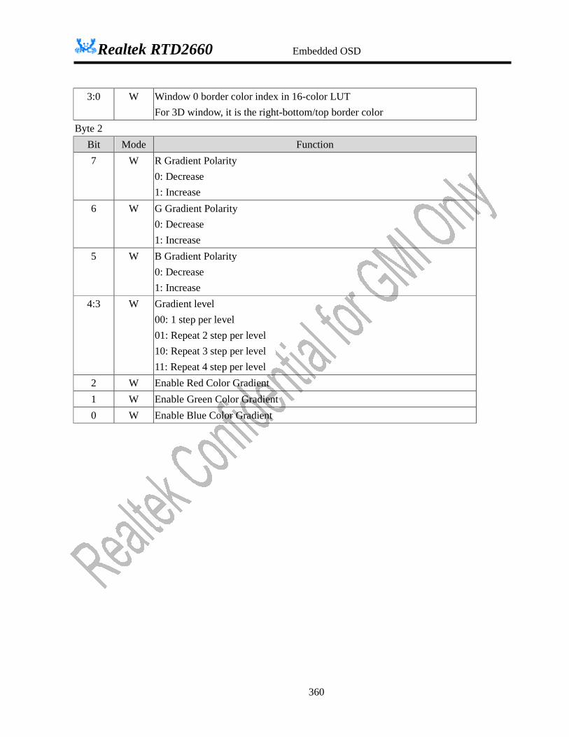
Realtek RTD2660 Embedded OSD
360
3:0 W Window 0 border color index in 16-color LUT For 3D window, it is the right-bottom/top border color
Byte 2 Bit Mode Function 7 W R Gradient Polarity
0: Decrease 1: Increase
6 W G Gradient Polarity 0: Decrease 1: Increase
5 W B Gradient Polarity 0: Decrease 1: Increase
4:3 W Gradient level 00: 1 step per level 01: Repeat 2 step per level 10: Repeat 3 step per level 11: Repeat 4 step per level
2 W Enable Red Color Gradient 1 W Enable Green Color Gradient 0 W Enable Blue Color Gradient
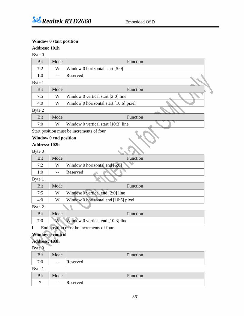
Realtek RTD2660 Embedded OSD
361
Window 0 start position Address: 101h Byte 0
Bit Mode Function 7:2 W Window 0 horizontal start [5:0] 1:0 -- Reserved
Byte 1 Bit Mode Function 7:5 W Window 0 vertical start [2:0] line 4:0 W Window 0 horizontal start [10:6] pixel
Byte 2 Bit Mode Function 7:0 W Window 0 vertical start [10:3] line
Start position must be increments of four. Window 0 end position Address: 102h Byte 0
Bit Mode Function 7:2 W Window 0 horizontal end [5:0] 1:0 -- Reserved
Byte 1 Bit Mode Function 7:5 W Window 0 vertical end [2:0] line 4:0 W Window 0 horizontal end [10:6] pixel
Byte 2 Bit Mode Function 7:0 W Window 0 vertical end [10:3] line
l End position must be increments of four. Window 0 control Address: 103h Byte 0
Bit Mode Function 7:0 -- Reserved
Byte 1 Bit Mode Function 7 -- Reserved
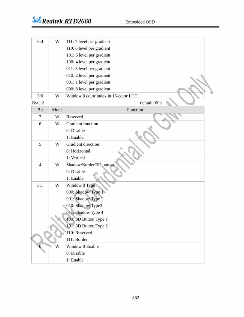
Realtek RTD2660 Embedded OSD
362
6:4 W 111: 7 level per gradient 110: 6 level per gradient 101: 5 level per gradient 100: 4 level per gradient 011: 3 level per gradient 010: 2 level per gradient 001: 1 level per gradient 000: 8 level per gradient
3:0 W Window 0 color index in 16-color LUT Byte 2 default: 00h
Bit Mode Function 7 W Reserved 6 W Gradient function
0: Disable 1: Enable
5 W Gradient direction 0: Horizontal 1: Vertical
4 W Shadow/Border/3D button 0: Disable 1: Enable
3:1 W Window 0 Type 000: Shadow Type 1 001: Shadow Type 2 010: Shadow Type3 011: Shadow Type 4 100: 3D Button Type 1 101: 3D Button Type 2 110: Reserved 111: Border
0 W Window 0 Enable 0: Disable 1: Enable

Realtek RTD2660 Embedded OSD
363
Window 1 Shadow/Border/Gradient Address: 104h Byte 0
Bit Mode Function 7:6 W Reserved 5:3 W Window 1 shadow/border width or 3D button thickness in pixel unit
000~111: 1 ~ 8 pixel 2:0 W Window 1 shadow/border height in line unit
000~111: 1 ~ 8 line It must be the same as bit[5:3] for 3D button thickness
Byte 1 Bit Mode Function 7:4 W Window 1 shadow color index in 16-color LUT
For 3D window, it is the left-top/bottom border color 3:0 W Window 1 border color index in 16-color LUT
For 3D window, it is the right-bottom/top border color Byte 2
Bit Mode Function 7:0 W Reserved
Window 1 start position Address: 105h Byte 0
Bit Mode Function 7:2 W Window 1 horizontal start [5:0] 1:0 -- Reserved
Byte 1 Bit Mode Function 7:5 W Window 1 vertical start [2:0] line 4:0 W Window 1 horizontal start [10:6] pixel
Byte 2 Bit Mode Function 7:0 W Window 1 vertical start [10:3] line
Start position must be increments of four. Window 1 end position
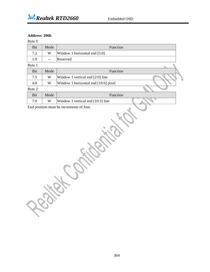
Realtek RTD2660 Embedded OSD
364
Address: 106h Byte 0
Bit Mode Function 7:2 W Window 1 horizontal end [5:0] 1:0 -- Reserved
Byte 1 Bit Mode Function 7:5 W Window 1 vertical end [2:0] line 4:0 W Window 1 horizontal end [10:6] pixel
Byte 2 Bit Mode Function 7:0 W Window 1 vertical end [10:3] line
End position must be increments of four.

Realtek RTD2660 Embedded OSD
365
Window 1 control Address: 107h Byte 0
Bit Mode Function 7:0 -- Reserved
Byte 1 Bit Mode Function 7:4 -- Reserved 3:0 W Window 1 color index in 16-color LUT
Byte 2 default: 00h Bit Mode Function 7:5 W Reserved 4 W Shadow/Border/3D button
0: Disable 1: Enable
3:1 W Window 1 Type 000: Shadow Type 1 001: Shadow Type 2 010: Shadow Type3 011: Shadow Type 4 100: 3D Button Type 1 101: 3D Button Type 2 110: Reserved 111: Border
0 W Window 1 Enable 0: Disable 1: Enable
Window 2 Shadow/Border/Gradient Address: 108h Byte 0
Bit Mode Function 7:6 W Reserved 5:3 W Window 2 shadow/border width or 3D button thickness in pixel unit
000~111: 1 ~ 8 pixel 2:0 W Window 2 shadow/border height in line unit
000~111: 1 ~ 8 line
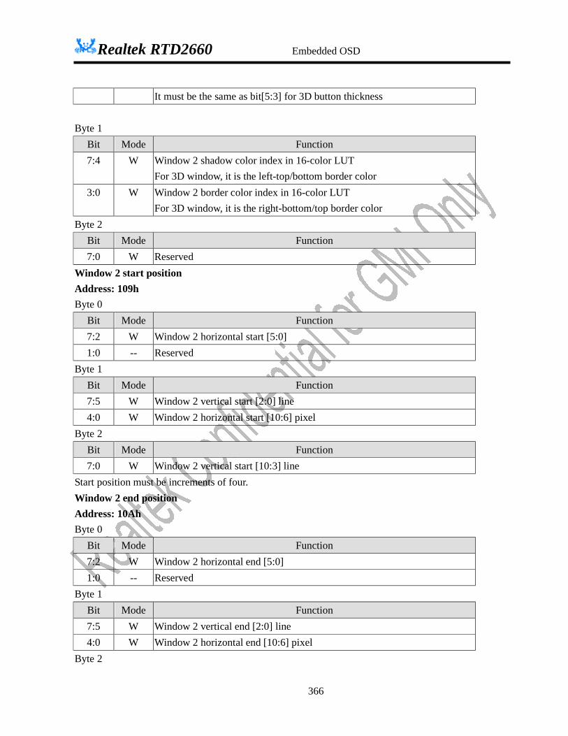
Realtek RTD2660 Embedded OSD
366
It must be the same as bit[5:3] for 3D button thickness Byte 1
Bit Mode Function 7:4 W Window 2 shadow color index in 16-color LUT
For 3D window, it is the left-top/bottom border color 3:0 W Window 2 border color index in 16-color LUT
For 3D window, it is the right-bottom/top border color Byte 2
Bit Mode Function 7:0 W Reserved
Window 2 start position Address: 109h Byte 0
Bit Mode Function 7:2 W Window 2 horizontal start [5:0] 1:0 -- Reserved
Byte 1 Bit Mode Function 7:5 W Window 2 vertical start [2:0] line 4:0 W Window 2 horizontal start [10:6] pixel
Byte 2 Bit Mode Function 7:0 W Window 2 vertical start [10:3] line
Start position must be increments of four. Window 2 end position Address: 10Ah Byte 0
Bit Mode Function 7:2 W Window 2 horizontal end [5:0] 1:0 -- Reserved
Byte 1 Bit Mode Function 7:5 W Window 2 vertical end [2:0] line 4:0 W Window 2 horizontal end [10:6] pixel
Byte 2
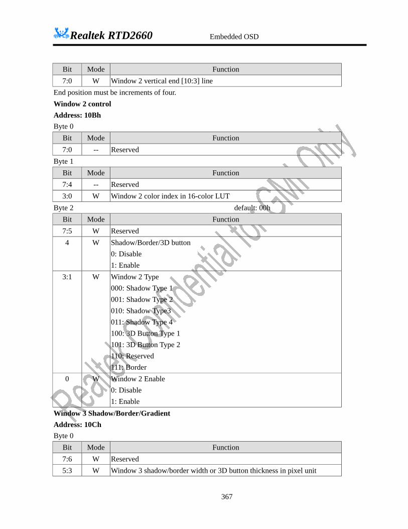
Realtek RTD2660 Embedded OSD
367
Bit Mode Function 7:0 W Window 2 vertical end [10:3] line
End position must be increments of four. Window 2 control Address: 10Bh Byte 0
Bit Mode Function 7:0 -- Reserved
Byte 1 Bit Mode Function 7:4 -- Reserved 3:0 W Window 2 color index in 16-color LUT
Byte 2 default: 00h Bit Mode Function 7:5 W Reserved 4 W Shadow/Border/3D button
0: Disable 1: Enable
3:1 W Window 2 Type 000: Shadow Type 1 001: Shadow Type 2 010: Shadow Type3 011: Shadow Type 4 100: 3D Button Type 1 101: 3D Button Type 2 110: Reserved 111: Border
0 W Window 2 Enable 0: Disable 1: Enable
Window 3 Shadow/Border/Gradient Address: 10Ch Byte 0
Bit Mode Function 7:6 W Reserved 5:3 W Window 3 shadow/border width or 3D button thickness in pixel unit

Realtek RTD2660 Embedded OSD
368
000~111: 1 ~ 8 pixel 2:0 W Window 3 shadow/border height in line unit
000~111: 1 ~ 8 line It must be the same as bit[5:3] for 3D button thickness
Byte 1 Bit Mode Function 7:4 W Window 3 shadow color index in 16-color LUT
For 3D window, it is the left-top/bottom border color 3:0 W Window 3 border color index in 16-color LUT
For 3D window, it is the right-bottom/top border color Byte 2
Bit Mode Function 7:0 W Reserved
Window 3 start position Address: 10Dh Byte 0
Bit Mode Function 7:2 W Window 3 horizontal start [5:0] 1:0 -- Reserved
Byte 1 Bit Mode Function 7:5 W Window 3 vertical start [2:0] line 4:0 W Window 3 horizontal start [10:6] pixel
Byte 2 Bit Mode Function 7:0 W Window 3 vertical start [10:3] line
Start position must be increments of four. Window 3 end position Address: 10Eh Byte 0
Bit Mode Function 7:2 W Window 3 horizontal end [5:0] 1:0 -- Reserved
Byte 1 Bit Mode Function 7:5 W Window 3 vertical end [2:0] line

Realtek RTD2660 Embedded OSD
369
4:0 W Window 3 horizontal end [10:6] pixel Byte 2
Bit Mode Function 7:0 W Window 3 vertical end [10:3] line
End position must be increments of four. Window 3 control Address: 10Fh Byte 0
Bit Mode Function 7:0 -- Reserved
Byte 1 Bit Mode Function 7:4 -- Reserved 3:0 W Window 3 color index in 16-color LUT
Byte 2 default: 00h Bit Mode Function 7:5 W Reserved 4 W Shadow/Border/3D button
0: Disable 1: Enable
3:1 W Window 3 Type 000: Shadow Type 1 001: Shadow Type 2 010: Shadow Type3 011: Shadow Type 4 100: 3D Button Type 1 101: 3D Button Type 2 110: Reserved 111: Border
0 W Window 3 Enable 0: Disable 1: Enable
Window 4 Shadow/Border/Gradient Address: 110h Byte 0

Realtek RTD2660 Embedded OSD
370
Bit Mode Function 7:6 W Reserved 5:3 W Window 4 shadow/border width or 3D button thickness in pixel unit
000~111: 1 ~ 8 pixel 2:0 W Window 4 shadow/border height in line unit
000~111: 1 ~ 8 line It must be the same as bit[5:3] for 3D button thickness
Byte 1 Bit Mode Function 7:4 W Window 4 shadow color index in 16-color LUT
For 3D window, it is the left-top/ bottom border color 3:0 W Window 4 border color index in 16-color LUT
For 3D window, it is the right-bottom/top border color Byte 2
Bit Mode Function 7:0 W Reserved
Window 4 start position Address: 111h Byte 0
Bit Mode Function 7:2 W Window 4 horizontal start [5:0] 2:0 -- Reserved
Byte 1 Bit Mode Function 7:5 W Window 4 vertical start [2:0] line 4:0 W Window 4 horizontal start [10:6] pixel
Byte 2 Bit Mode Function 7:0 W Window 4 vertical start [10:3] line
Window 4 end position Address: 112h Byte 0
Bit Mode Function 7:2 W Window 4 horizontal end [5:0] 1:0 -- Reserved
Byte 1
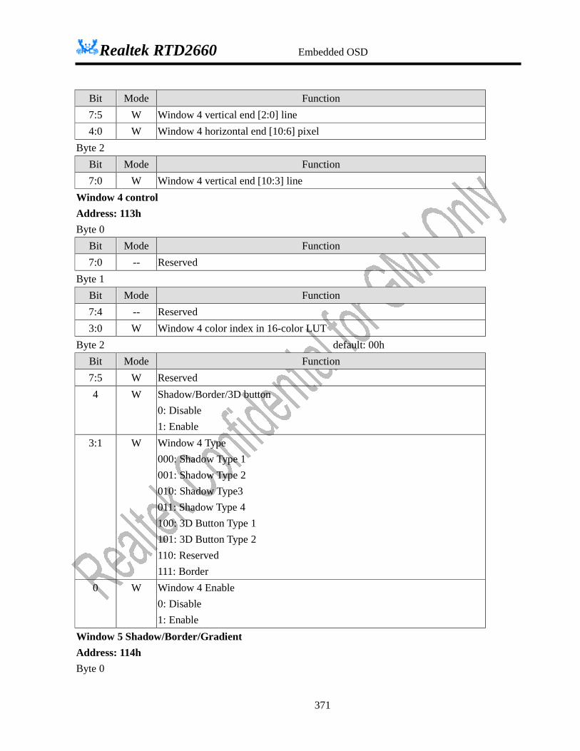
Realtek RTD2660 Embedded OSD
371
Bit Mode Function 7:5 W Window 4 vertical end [2:0] line 4:0 W Window 4 horizontal end [10:6] pixel
Byte 2 Bit Mode Function 7:0 W Window 4 vertical end [10:3] line
Window 4 control Address: 113h Byte 0
Bit Mode Function 7:0 -- Reserved
Byte 1 Bit Mode Function 7:4 -- Reserved 3:0 W Window 4 color index in 16-color LUT
Byte 2 default: 00h Bit Mode Function 7:5 W Reserved 4 W Shadow/Border/3D button
0: Disable 1: Enable
3:1 W Window 4 Type 000: Shadow Type 1 001: Shadow Type 2 010: Shadow Type3 011: Shadow Type 4 100: 3D Button Type 1 101: 3D Button Type 2 110: Reserved 111: Border
0 W Window 4 Enable 0: Disable 1: Enable
Window 5 Shadow/Border/Gradient Address: 114h Byte 0
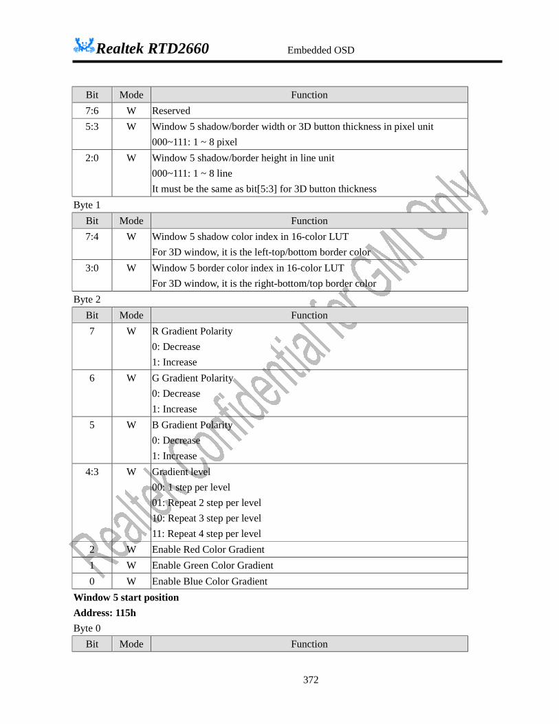
Realtek RTD2660 Embedded OSD
372
Bit Mode Function 7:6 W Reserved 5:3 W Window 5 shadow/border width or 3D button thickness in pixel unit
000~111: 1 ~ 8 pixel 2:0 W Window 5 shadow/border height in line unit
000~111: 1 ~ 8 line It must be the same as bit[5:3] for 3D button thickness
Byte 1 Bit Mode Function 7:4 W Window 5 shadow color index in 16-color LUT
For 3D window, it is the left-top/bottom border color 3:0 W Window 5 border color index in 16-color LUT
For 3D window, it is the right-bottom/top border color Byte 2
Bit Mode Function 7 W R Gradient Polarity
0: Decrease 1: Increase
6 W G Gradient Polarity 0: Decrease 1: Increase
5 W B Gradient Polarity 0: Decrease 1: Increase
4:3 W Gradient level 00: 1 step per level 01: Repeat 2 step per level 10: Repeat 3 step per level 11: Repeat 4 step per level
2 W Enable Red Color Gradient 1 W Enable Green Color Gradient 0 W Enable Blue Color Gradient
Window 5 start position Address: 115h Byte 0
Bit Mode Function

Realtek RTD2660 Embedded OSD
373
7:2 W Window 5 horizontal start [5:0] 1:0 -- Reserved
Byte 1 Bit Mode Function 7:5 W Window 5 vertical start [2:0] line 4:0 W Window 5 horizontal start [10:6] pixel
Byte 2 Bit Mode Function 7:0 W Window 5 vertical start [10:3] line
Window 5 end position Address: 116h Byte 0
Bit Mode Function 7:2 W Window 5 horizontal end [5:0] 1:0 -- Reserved
Byte 1 Bit Mode Function 7:5 W Window 5 vertical end [2:0] line 4:0 W Window 5 horizontal end [10:6] pixel
Byte 2 Bit Mode Function 7:0 W Window 5 vertical end [10:3] line
Window 5 control Address: 117h Byte 0
Bit Mode Function 7:0 -- Reserved
Byte 1 Bit Mode Function 7 -- Reserved
6:4 W 111: 7 level per gradient 110: 6 level per gradient 101: 5 level per gradient 100: 4 level per gradient 011: 3 level per gradient 010: 2 level per gradient

Realtek RTD2660 Embedded OSD
374
001: 1 level per gradient 000: 8 level per gradient
3:0 W Window 5 color index in 16-color LUT Byte 2 default: 00h
Bit Mode Function 7 W Reserved 6 W Gradient function
0: Disable 1: Enable
5 W Gradient direction 0: Horizontal 1: Vertical
4 W Shadow/Border/3D button 0: Disable 1: Enable
3:1 W Window 5 Type 000: Shadow Type 1 001: Shadow Type 2 010: Shadow Type3 011: Shadow Type 4 100: 3D Button Type 1 101: 3D Button Type 2 110: Reserved 111: Border
0 W Window 5 Enable 0: Disable 1: Enable
Window 6 Shadow/Border/Gradient Address: 118h Byte 0
Bit Mode Function 7:6 W Reserved 5:3 W Window 6 shadow/border width or 3D button thickness in pixel unit
000~111: 1 ~ 8 pixel
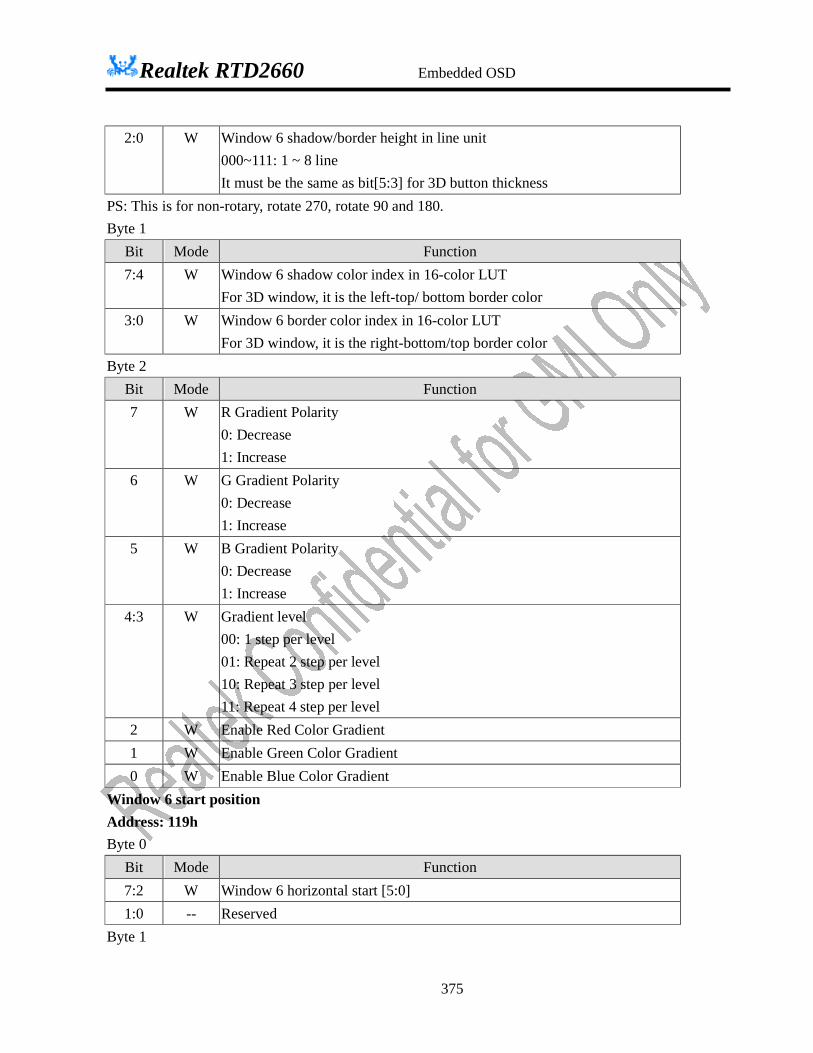
Realtek RTD2660 Embedded OSD
375
2:0 W Window 6 shadow/border height in line unit 000~111: 1 ~ 8 line It must be the same as bit[5:3] for 3D button thickness
PS: This is for non-rotary, rotate 270, rotate 90 and 180. Byte 1
Bit Mode Function 7:4 W Window 6 shadow color index in 16-color LUT
For 3D window, it is the left-top/ bottom border color 3:0 W Window 6 border color index in 16-color LUT
For 3D window, it is the right-bottom/top border color Byte 2
Bit Mode Function 7 W R Gradient Polarity
0: Decrease 1: Increase
6 W G Gradient Polarity 0: Decrease 1: Increase
5 W B Gradient Polarity 0: Decrease 1: Increase
4:3 W Gradient level 00: 1 step per level 01: Repeat 2 step per level 10: Repeat 3 step per level 11: Repeat 4 step per level
2 W Enable Red Color Gradient 1 W Enable Green Color Gradient 0 W Enable Blue Color Gradient
Window 6 start position Address: 119h Byte 0
Bit Mode Function 7:2 W Window 6 horizontal start [5:0] 1:0 -- Reserved
Byte 1
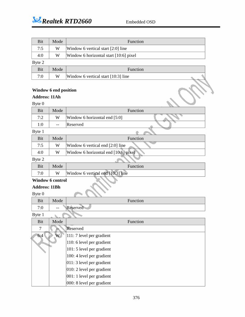
Realtek RTD2660 Embedded OSD
376
Bit Mode Function 7:5 W Window 6 vertical start [2:0] line 4:0 W Window 6 horizontal start [10:6] pixel
Byte 2 Bit Mode Function 7:0 W Window 6 vertical start [10:3] line
Window 6 end position Address: 11Ah Byte 0
Bit Mode Function 7:2 W Window 6 horizontal end [5:0] 1:0 -- Reserved
Byte 1 Bit Mode Function 7:5 W Window 6 vertical end [2:0] line 4:0 W Window 6 horizontal end [10:6] pixel
Byte 2 Bit Mode Function 7:0 W Window 6 vertical end [10:3] line
Window 6 control Address: 11Bh Byte 0
Bit Mode Function 7:0 -- Reserved
Byte 1 Bit Mode Function 7 -- Reserved
6:4 W 111: 7 level per gradient 110: 6 level per gradient 101: 5 level per gradient 100: 4 level per gradient 011: 3 level per gradient 010: 2 level per gradient 001: 1 level per gradient 000: 8 level per gradient
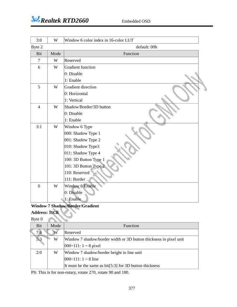
Realtek RTD2660 Embedded OSD
377
3:0 W Window 6 color index in 16-color LUT Byte 2 default: 00h
Bit Mode Function 7 W Reserved 6 W Gradient function
0: Disable 1: Enable
5 W Gradient direction 0: Horizontal 1: Vertical
4 W Shadow/Border/3D button 0: Disable 1: Enable
3:1 W Window 6 Type 000: Shadow Type 1 001: Shadow Type 2 010: Shadow Type3 011: Shadow Type 4 100: 3D Button Type 1 101: 3D Button Type 2 110: Reserved 111: Border
0 W Window 6 Enable 0: Disable 1: Enable
Window 7 Shadow/Border/Gradient Address: 11Ch Byte 0
Bit Mode Function 7:6 W Reserved 5:3 W Window 7 shadow/border width or 3D button thickness in pixel unit
000~111: 1 ~ 8 pixel 2:0 W Window 7 shadow/border height in line unit
000~111: 1 ~ 8 line It must be the same as bit[5:3] for 3D button thickness
PS: This is for non-rotary, rotate 270, rotate 90 and 180.

Realtek RTD2660 Embedded OSD
378
Byte 1 Bit Mode Function 7:4 W Window 7 shadow color index in 16-color LUT
For 3D window, it is the left-top/bottom border color 3:0 W Window 7 border color index in 16-color LUT
For 3D window, it is the right-bottom/top border color Byte 2
Bit Mode Function 7 W R Gradient Polarity
0: Decrease 1: Increase
6 W G Gradient Polarity 0: Decrease 1: Increase
5 W B Gradient Polarity 0: Decrease 1: Increase
4:3 W Gradient level 00: 1 step per level 01: Repeat 2 step per level 10: Repeat 3 step per level 11: Repeat 4 step per level
2 W Enable Red Color Gradient 1 W Enable Green Color Gradient 0 W Enable Blue Color Gradient
Window 7 start position Address: 11Dh Byte 0
Bit Mode Function 7:2 W Window 7 horizontal start [5:0] 1:0 -- Reserved
Byte 1 Bit Mode Function 7:5 W Window 7 vertical start [2:0] line 4:0 W Window 7 horizontal start [10:6] pixel
Byte 2
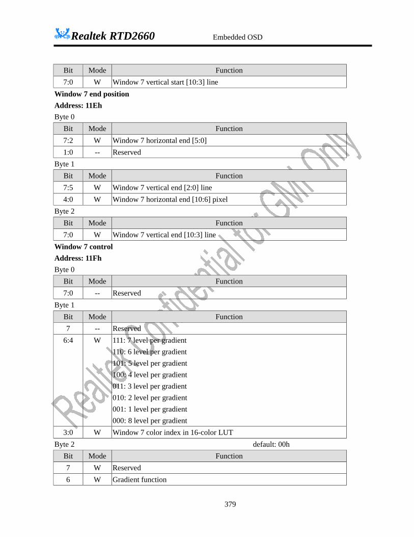
Realtek RTD2660 Embedded OSD
379
Bit Mode Function 7:0 W Window 7 vertical start [10:3] line
Window 7 end position Address: 11Eh Byte 0
Bit Mode Function 7:2 W Window 7 horizontal end [5:0] 1:0 -- Reserved
Byte 1 Bit Mode Function 7:5 W Window 7 vertical end [2:0] line 4:0 W Window 7 horizontal end [10:6] pixel
Byte 2 Bit Mode Function 7:0 W Window 7 vertical end [10:3] line
Window 7 control Address: 11Fh Byte 0
Bit Mode Function 7:0 -- Reserved
Byte 1 Bit Mode Function 7 -- Reserved
6:4 W 111: 7 level per gradient 110: 6 level per gradient 101: 5 level per gradient 100: 4 level per gradient 011: 3 level per gradient 010: 2 level per gradient 001: 1 level per gradient 000: 8 level per gradient
3:0 W Window 7 color index in 16-color LUT Byte 2 default: 00h
Bit Mode Function 7 W Reserved 6 W Gradient function

Realtek RTD2660 Embedded OSD
380
0: Disable 1: Enable
5 W Gradient direction 0: Horizontal 1: Vertical
4 W Shadow/Border/3D button 0: Disable 1: Enable
3:1 W Window 7 Type 000: Shadow Type 1 001: Shadow Type 2 010: Shadow Type3 011: Shadow Type 4 100: 3D Button Type 1 101: 3D Button Type 2 110: Reserved 111: Border
0 W Window 7 Enable 0: Disable 1: Enable

Realtek RTD2660 Embedded OSD
381
3D Button Type 1
3D Button Type 2

Realtek RTD2660 Embedded OSD
382
Type 1 Type 2 Type 3 Type 4
width
height
Shadow in all direction
OSD appear range transparent
start
end
Window mask fade/in out function

Realtek RTD2660 Embedded OSD
383
Frame control registers Address: 000h Byte 0
Bit Mode Function 7:0 R/W Vertical Delay [10:3]
The bits define the vertical starting address. Total 2048 step unit: 1 line Vertical delay minimum should set 1 Byte 1
Bit Mode Function 7:0 R/W Horizontal Delay [9:2]
The bits define the horizontal starting address. Total 1024 step unit:4 pixels Horizontal delay minimum should set 2 Byte 2 default: xxxx_xxx0b
Bit Mode Function 7:6 R/W Horizontal Delay bit [1:0] 5:3 R/W Vertical Delay [2:0] 2:1 R/W Display zone, for smaller character width
00: middle 01: left 10: right 11: reserved
0 R/W OSD enable 0: OSD circuit is inactivated 1: OSD circuit is activated
l When OSD is disabled, Double Width (address 0x002 Byte1[1]) must be disabled to save power.
l These three bytes have their own double-buffer.

Realtek RTD2660 Embedded OSD
384
Address 001h ~ Address002h are reserved Address: 003h Byte 0 Default: 00h
Bit Mode Function 7 R/W Specific color blending (blending type 2)
0: Disable 1: Enable
6:5 R/W Window 7special function 00: disable 01: blending (blending type 3) 10: window 7 mask region appear 11: window 7 mask region transparent
4 R/W OSD vertical start input signal source select 0: Select DVS as OSD VSYNC input 1: Select ENA as OSD VSYNC input
3:0 R/W Blending color from 16-color LUT (blending type 2) Byte 1 Default: 00h
Bit Mode Function 7:4 R/W Char shadow/border color 3: 2 R/W Alpha blending type (blending type 1)
00: Disable alpha blending 01: Only window blending 10: All blending 11: Window and Character background blending
1 R/W Double width enable (For all OSD including windows and characters) 0: Normal 1: Double
0 R/W Double Height enable (For all OSD including windows and characters) 0: Normal 1: Double
Total blending area = blending type1 area + blending type 2 area + blending type 3 area Byte 2 Default: 00h
Bit Mode Function 7:6 R/W Font downloaded swap control
0x: No swap

Realtek RTD2660 Embedded OSD
385
10: CCW 11: CW
5 R Buffer Empty 0: Empty 1: Not Empty
4 R Buffer Valid 0: Done 1: Buffer is writing to SDRAM
3 R/W Reset Buffer Write 1 to reset and auto-clear after finished.
2 R/W Hardware Rotation Enable 0: Disable 1: Enable (Default) OSD compression function must be enabled simultaneously.
1 R/W Global Blinking Enable 0: Disable 1: Enable
0 R/W Rotation 0: Normal (data latch 24 bit per 24 bit) 1: Rotation (data latch 18 bit per 24 bit)
Bit 7 6 5 4 3 2 1 0
Firmware A B C D E F G H CW A E B F C G D H
CCW E A F B G C H D
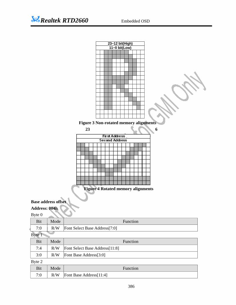
Realtek RTD2660 Embedded OSD
386
Figure 3 Non-rotated memory alignments 23 6
Figure 4 Rotated memory alignments
Base address offset Address: 004h Byte 0
Bit Mode Function 7:0 R/W Font Select Base Address[7:0]
Byte 1 Bit Mode Function 7:4 R/W Font Select Base Address[11:8] 3:0 R/W Font Base Address[3:0]
Byte 2 Bit Mode Function 7:0 R/W Font Base Address[11:4]
23~12 bit(High)11~0 bit(Low)

Realtek RTD2660 Embedded OSD
387
When OSD Special Function for POP-ON is enabled (OSD[008]), Font Select Base Address here will not be effective.
OSD Compression Address: 005h Byte 0
Bit Mode Function 7:4 R/W 4-bit value for VLC code 0 3:0 R/W 4-bit value for VLC code 100
Byte 1 Bit Mode Function 7:4 R/W 4-bit value for VLC code 1010 3:0 R/W 4-bit value for VLC code 1011
Byte 2 Bit Mode Function 7:4 R/W 4-bit value for VLC code 1100 3:0 R/W 4-bit value for VLC code 1101 0
Address: 006h Byte 0
Bit Mode Function 7:4 R/W 4-bit value for VLC code 1101 1 3:0 R/W 4-bit value for VLC code 1110 0
Byte 1 Bit Mode Function 7:4 R/W 4-bit value for VLC code 1110 10 3:0 R/W 4-bit value for VLC code 1110 11
Byte 2 Bit Mode Function 7:4 R/W 4-bit value for VLC code 1111 00 3:0 R/W 4-bit value for VLC code 1111 01
Address: 007h Byte 0
Bit Mode Function

Realtek RTD2660 Embedded OSD
388
7:4 R/W 4-bit value for VLC code 1111 100 3:0 R/W 4-bit value for VLC code 1111 101
Byte 1 Bit Mode Function 7:4 R/W 4-bit value for VLC code 1111 110 3:0 R/W 4-bit value for VLC code 1111 1110
Byte 2 default: xxxx_xxx0b Bit Mode Function 7:1 -- reserved 0 R/W OSD compression (4bit/symbol, VLC code 1111_1111 represents the end of
data) (only for SRAM) 0: disable 1: enable
Note:
1. If enable OSD compression or auto load (double buffer), only one byte can be read after writing address at 0x90,
0x91.
2. For OSD compression, MSB 4 bits of original byte is first transferred to corresponding VLC code, and then LSB 4
bits is transferred. VLC code is placed from LSB to MSB of compression font. For example, 4-bit value for VLC
code 1100 is 4’b0101, and 4-bit value for VLC code 100 is 4’b0001. Original data 0x15 is transferred to
compression x0011001.
3. OSD double buffer and compression can’t be enabled simultaneous.
4. When power-down mode or lack of crystal clock, OSD compression font can’t be write.
5. After OSD enable, it is better to delay 1 DVS to start writing OSD compression data.
OSD Special Function Address: 008h Byte 0 Default: 0x00
Bit Mode Function 7 R/W OSD Special Function Enable
0: Disable 1: Enable
6 R/W OSD Special Function Select (Effective only when Bit[7]=1) 0: ROLL-UP 1: POP-ON
5 R/W OSD Vertical Boundary Function Enable 0: Disable 1: Enable

Realtek RTD2660 Embedded OSD
389
4:1 R/W Reserved to 0 0 R/W Display Base Select (Effective only when Bit[7:6]=11`b)
0: Base 0 1: Base 1
Byte 1 Default: 0x00 Bit Mode Function 7:0 R/W Row Command Base 0 [7:0]
Byte 2 Default: 0x00 Bit Mode Function 7:0 R/W Row Command Base 1 [7:0]
Address: 009h Byte 0 Default: 0x00
Bit Mode Function 7:4 R/W Font Select Base 0 [11:8] 3:0 R/W Font Select Base 1 [11:8]
Byte 1 Default: 0x00 Bit Mode Function 7:0 R/W Font Select Base 0 [7:0]
Byte 2 Default: 0x00 Bit Mode Function 7:0 R/W Font Select Base 1 [7:0] (Not effective when ROLL-UP)
Address: 00Ah Byte 0 Default: 0x00
Bit Mode Function 7 R/W Reserved
6:4 R/W OSD Vertical Upper Boundary [10:8] 3 R/W Reserved
2:0 R/W OSD Vertical Lower Boundary [10:8] Byte 1 Default: 0x00
Bit Mode Function 7:0 R/W OSD Vertical Upper Boundary [7:0]
Byte 2 Default: 0x00 Bit Mode Function 7:0 R/W OSD Vertical Lower Boundary [7:0]
Note:

Realtek RTD2660 Embedded OSD
390
1. When OSD Special Function for POP-ON is enabled, Font Select Base Address in OSD[004] will not be effective
anymore.
2. When OSD Vertical Boundary Function is enabled, OSD image above upper boundary and below lower boundary
will be invisible.
3. When ROLL-UP function is enabled, OSD will always start from the row-command pointed by Base0, and after the
row-command pointed by Base1 has been dealt with, the next row-command will be the first one in OSD SRAM.
Row-command processing will terminate in the row-command before the one pointed by Base0. (For example, R1
is pointed by Base0, and R5 is pointed by Base1. OSD will show R1 as the first row, followed by R2, R3, R4, R5,
and R0 as last row.)
4. When POP-ON function is enabled, OSD will start from the row command pointed by the base selected as display
base(selected by OSD[008][0.0]), and terminate when end-command is encountered. That is, all row-command will
be separated into two non-overlay subset which is enclosed by the row-command pointed by base and
end-command.
OSD SRAM (Map and font registers)
R0 R1 R2 …. Rn End C01 C02 B03 C04 … C11 C12 C13 …
… …
… Cn1 Cn2 … 1-bit font start … …
… 2-bit font start … …
4-bit font start … … …
16.5k bytes SRAM
1. Row Command
R0 R1 R2 R3 R…. Rn End
Row Command R0~Rn represent the start of new row. Each command contains 3 bytes data which define the length
of a row and other attributes. OSD End Command represent the end of OSD. R0 is set in address 0 of SRAM.
2. Character/Blank Command (Font Select)

Realtek RTD2660 Embedded OSD
391
Character Command is used to select which character font is show. Each command contains three bytes which specify
its attribute and 1,2 or 4bit per pixel. Blank Command represents blank pixel to separate the preceding character and
following character. Use two or more Blank Command if the character distance exceeds 255 pixel.
The Font Select Base Address in Frame Control Register represents the address of the first character in Row 0, that is,
C01 in the above figure. The following character/blank is write in the next address. C11 represents the first character
in Row1, C12 represents the second character in Row1, and so on.
The address of the first character Cn1 in Row n = Font Select Base Address + Row 0 font base length + Row 1 font
base length + …+Row n-1 font base length.
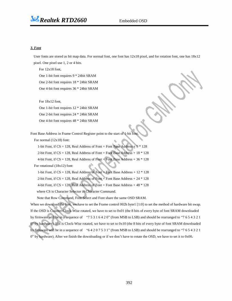
Realtek RTD2660 Embedded OSD
392
3. Font
User fonts are stored as bit map data. For normal font, one font has 12x18 pixel, and for rotation font, one has 18x12
pixel. One pixel use 1, 2 or 4 bits.
For 12x18 font,
One 1-bit font requires 9 * 24bit SRAM
One 2-bit font requires 18 * 24bit SRAM
One 4-bit font requires 36 * 24bit SRAM
For 18x12 font,
One 1-bit font requires 12 * 24bit SRAM
One 2-bit font requires 24 * 24bit SRAM
One 4-bit font requires 48 * 24bit SRAM
Font Base Address in Frame Control Register point to the start of 1-bit font.
For normal (12x18) font:
1-bit Font, if CS = 128, Real Address of Font = Font Base Address + 9 * 128
2-bit Font, if CS = 128, Real Address of Font = Font Base Address + 18 * 128
4-bit Font, if CS = 128, Real Address of Font = Font Base Address + 36 * 128
For rotational (18x12) font:
1-bit Font, if CS = 128, Real Address of Font = Font Base Address + 12 * 128
2-bit Font, if CS = 128, Real Address of Font = Font Base Address + 24 * 128
4-bit Font, if CS = 128, Real Address of Font = Font Base Address + 48 * 128
where CS is Character Selector in Character Command.
Note that Row Command, Font Select and Font share the same OSD SRAM.
When we download the font, we have to set the Frame control 002h byte1 [1:0] to set the method of hardware bit swap.
If the OSD is Counter-Clock-Wise rotated, we have to set to 0x01 (the 8 bits of every byte of font SRAM downloaded
by firmware will be in a sequence of “7 5 3 1 6 4 2 0” (from MSB to LSB) and should be rearranged to “7 6 5 4 3 2 1
0” by hardware). If it is Clock-Wise rotated, we have to set to 0x10 (the 8 bits of every byte of font SRAM downloaded
by firmware will be in a sequence of “6 4 2 0 7 5 3 1” (from MSB to LSB) and should be rearranged to “7 6 5 4 3 2 1
0” by hardware). After we finish the downloading or if we don’t have to rotate the OSD, we have to set it to 0x00.

Realtek RTD2660 Embedded OSD
393
Row Command Byte 0
Bit Mode Function 7 W 1: Row Start Command
0: OSD End Command Each row must start with row-command, last word of OSD map must be end-command
6 R/W VBI OSD function enable 0: normal OSD function as usual 1: support VBI OSD functions like underline, B/F separated blink and 512 fonts select
5 W Reserved 4:2 W Character border/shadow
000: None 001: Border 100: Shadow (left-top) 101: Shadow (left-bottom) 110: Shadow (right-top) 111: Shadow (right-bottom)
1 W Double character width 0: x1 1: x2
0 W Double character height 0: x1 1: x2
Byte 1 Bit Mode Function 7:3 W Row height (1~32) 2:0 W Column space
0~7 pixel column space When Char is doubled, so is column space.
Notice: When character height/width is doubled, the row height/column space definition also twice. If the row height is larger than character height, the effect is just like space between rows. If it is smaller than character height, it will drop last several bottom line of character.
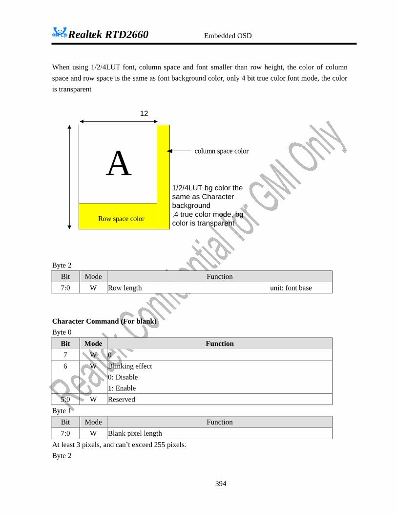
Realtek RTD2660 Embedded OSD
394
When using 1/2/4LUT font, column space and font smaller than row height, the color of column space and row space is the same as font background color, only 4 bit true color font mode, the color is transparent
12
25 A1/2/4LUT bg color thesame as Characterbackground,4 true color mode, bgcolor is transparentRow space color
column space color
Byte 2
Bit Mode Function 7:0 W Row length unit: font base
Character Command (For blank) Byte 0
Bit Mode Function 7 W 0 6 W Blinking effect
0: Disable 1: Enable
5:0 W Reserved Byte 1
Bit Mode Function 7:0 W Blank pixel length
At least 3 pixels, and can’t exceed 255 pixels. Byte 2

Realtek RTD2660 Embedded OSD
395
Bit Mode Function 7:5 W Reserved 4 W Reserved
3:0 W Blank color – select one of 16-color LUT (0 is special for transparent)
Character Command (For 1-bit RAM font) Byte 0
Bit Mode Function 7 W 1 6 W Character Blinking effect
0: Disable 1: Enable
5:4 W 00 (Font type 00: 1-bit RAM Font 01: 4-bit RAM Font 1x: 2-bit RAM Font)
3:0 W VBI OSD disable: Character width (only for 1-pixel font, doubled when specifying double-width in Row/Blank command register) For 12x18 font: 0100: 4-pixel 0101: 5-pixel 0110: 6-pixel 0111: 7-pixel 1000: 8-pixel 1001: 9-pixel 1010: 10-pixel 1011:11-pixel 1100: 12-pixel For 18x12 Font (rotated) 0000: 4-pixel 0001: 5-pixel 0010: 6-pixel 0011: 7-pixel 0100: 8-pixel 0101: 9-pixel 0110: 10-pixel 0111: 11-pixel 1000: 12-pixel 1001:13-pixel 1010:14-pixel 1011:15-pixel 1100: 16-pixel 1101:17-pixel 1110:18-pixel VBI OSD enable: While VBI OSD enable, 1 bit font will be NO rotated and 12-pixel fonts always. Then the [3:0] setting will be as following: [3]: character select[8] support 512 font while VBI OSD enable

Realtek RTD2660 Embedded OSD
396
[2]: additional blinking effect {[6], [2]} 00: NO blink for both F/B 01: Only blink for Foreground 10: Only blink for Background 11: Both blink for F/B [1]: Underline enable underline will be at 17th & 18th line and got the same color with foreground [0]: Reserved
When using border/shadow/ effect, the width of the 1-bit font should at least 6 pixel. Byte 1
Bit Mode Function 7:0 W Character Select [7:0]
Byte 2 Bit Mode Function 7:4 W Foreground color
Select one of 16-color from color LUT 3:0 W Background color
Select one of 16-color from color LUT (0 is special for transparent) Character command (For 2-bit RAM Font) Byte 0
Bit Mode Function 7 W 1 6 W MSB of Foreground color 11, Background 00 5 W 1 4 W MSB of Foreground color 10, Foreground 01
3:1 W Foreground color 11 Select one of 8 color from color LUT Add Byte0 [6] as MSB for 16-color LUT.
0 W Background color 00 Bit[2] Select one of 8 color from color LUT
Byte 1 Bit Mode Function
Realtek RTD2660 Embedded OSD
397
7:0 W Character Select [7:0] Byte 2
Bit Mode Function 7:6 W Background color 00 Bit[1:0]
Select one of 8 color from color LUT While 0 is special for transparent Add Byte0 [6] as MSB for 16-color LUT. Once we fill 0000 or 1000(MSB follow Byte0[6]), BG appears transparent.
5:3 W Foreground color 10 Select one of 8 color from color LUT Add Byte0 [4] as MSB for 16-color LUT.
2:0 W Foreground color 01 Select one of 8 color from color LUT Add Byte0 [4] as MSB for 16-color LUT.
Character command (For 4-bit RAM font) Byte 0
Bit Mode Function 7 W 1 6 W Character Blinking effect
0: Disable 1: Enable
5:4 W 01 (Font type 00: 1-bit RAM Font 01: 4-bit RAM Font 1x: 2-bit RAM Font)
3:0 W (for Byte1[7] = 0) select one color from 16-color LUT as background (for Byte1[7] = 1) Red color level MSB 4 bits for 8 bits color level (LSB 4 bits are 1111)
Byte 1 Bit Mode Function 7 W 0: 4bit Look Up Table, 0000’b is transparent.
1: 3bit specify R,G,B pattern, color level defined in Byte0[3:0],Byte2. One

Realtek RTD2660 Embedded OSD
398
mask bit defines foreground or background. 6:0 W Character Select [6:0]
l When 4-bit look-up table mode,color of column space is the same as background. l When 4-bit look-up table mode and pixel value is 0000, and byte0[3:0]=0000 means
transparent. l When true color mode and pixel value is 0000,it is transparent。 Byte 2
Bit Mode Function 7:4 W (for Byte1[7] = 1)
Green color level MSB 4 bits for 8 bits color level (LSB 4 bits are 1111)
3:0 W (for Byte1[7] = 1) Blue color level MSB 4 bits for 8 bits color level (LSB 4 bits are 1111)

Realtek RTD2660 Embedded OSD
399
4. Electric Specification DC Characteristics Table 2 Absolute Maximum Ratings
PARAMETER SYMBOL MIN TYP MAX UNITS
Voltage on Input (5V tolerant) VIN -1 5 V
Electrostatic Discharge VESD ±2.5 kV
Latch-Up ILA ±100 mA
Ambient Operating Temperature TA 0 70 ºC
Storage temperature (plastic) TSTG -55 125 ºC
Thermal Resistance (Junction to Air) θJA 25 ºC/W
Junction Acceptable Temperature Tj 125 ºC
Table 3 DC Characteristics/Operating Condition (0℃<TA<70℃)
【Power consumption:Embedded MCU】 Dot-pattern(check_11). 【1】 VGA-in: 1600x1200/75Hz,display to 1680x1050/75Hz,DCLK=170MHz.
Pattern Generator:『Chroma 2227』;Pattern Name:『Dot』pattern 【2】 Video Decoder-in:DVD-player;AV-in;display to 1680x1050
Power Name Voltage Operating(mA) Power saving(mA)
Power down(mA)
VCCK(core)(VGA) 1.8V 438 14.9 5.9 VCCK(core) 1.8V 455 8.5 6.1
VCCK(core)(Video Decoder) 1.8V 232 8.6 6.1 ADC_VDD 1.8V 123 0.1 0.1
VDD 3.3V 173 19.9 19.9 VADC_VDD 3.3V 65.6 0.1 0.1 PVCC(LVDS) 3.3V 78.5 2.5 2.5 PVCC(TTL) 3.3V 34.1 12.8 12.8
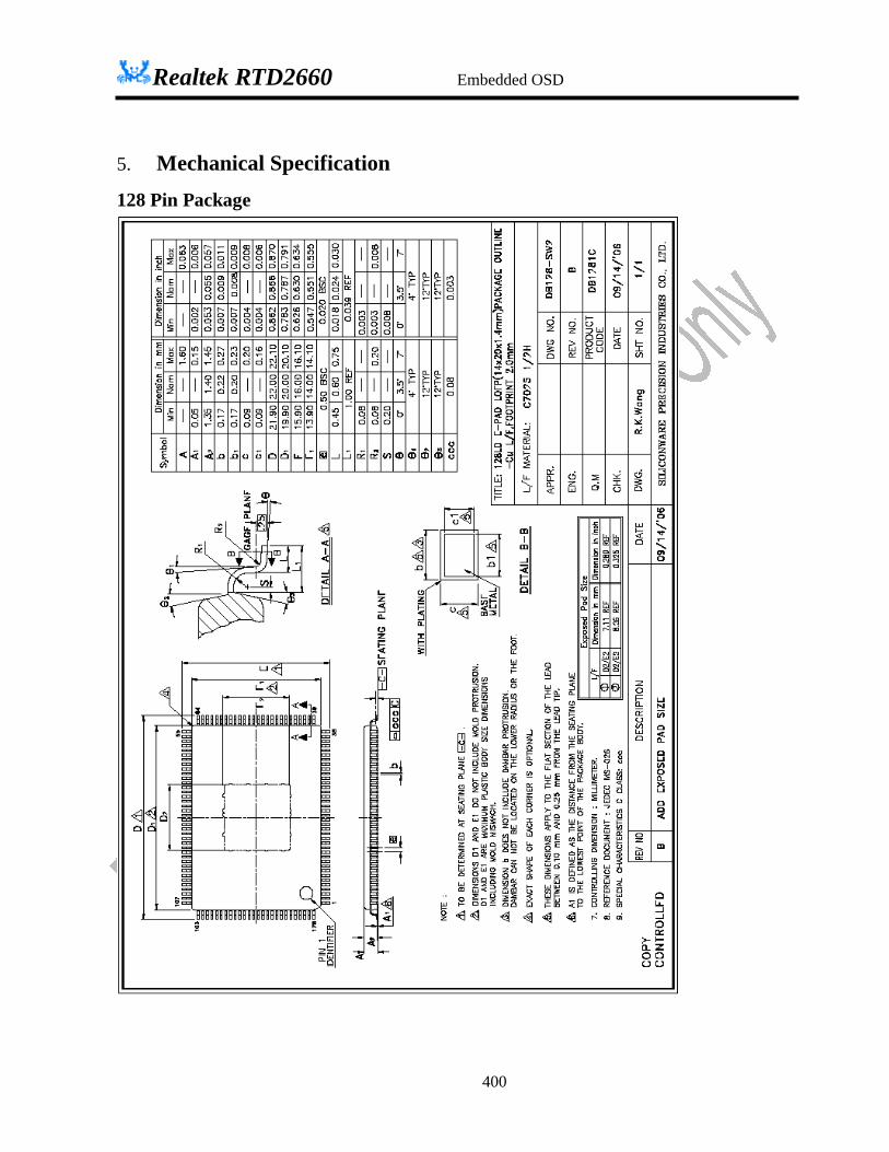
Realtek RTD2660 Embedded OSD
400
5. Mechanical Specification
128 Pin Package

Realtek RTD2660 Embedded OSD
401
6. Ordering Information