Embed Size (px)
Citation preview

12Three Phase Controlled ecti ers
12.1 Introduction
Three-phase controlled rectifiers have a wide range of applica-
tions, from small rectifiers to large high voltage direct current
(HVDC) transmission systems. They are used for electro-
chemical processes, many kinds of motor drives, traction
equipment, controlled power supplies, and many other appli-
cations. From the point of view of the commutation process,
they can be classified into two important categories: line-
commutated controlled rectifiers (thyristor rectifiers) and
force-commutated PWM rectifiers.
12.2 Line-Commutated ControlledRectifiers
12.2.1 Three-Phase alf- ave Rectifier
Figure 12.1 shows the three-phase half-wave rectifier topology.
To control the load voltage, the half-wave rectifier uses three
common-cathode thyristor arrangement. In this figure, the
power supply and the transformer are assumed ideal. The
thyristor will conduct (ON state), when the anode-to-cathode
voltage AK is positive, and a firing current pulse iG is applied
to the gate terminal. Delaying the firing pulse by an angle acontrols the load voltage. As shown in Fig. 12.2, the firing
angle a is measured from the crossing point between the phase
supply voltages. At that point, the anode-to-cathode thyristor
voltage AK begins to be positive. Figure 12.3 shows that the
possible range for gating delay is between a ¼ 0� and
a ¼ 180�, but because of commutation problems in actual
situations, the maximum firing angle is limited to �160�. As
shown in Fig. 12.4, when the load is resistive, current id has the
same waveform as the load voltage. As the load becomes more
and more inductive, the current flattens and finally becomes
constant. The thyristor goes to the nonconducting condition
(OFF state) when the following thyristor is switched ON, or
the current tries to reach a negative value.
With the help of Fig. 12.2, the load average voltage can be
evaluated and is given by
VD ¼Vmax
2=3p
ðp=3þa
p=3þacosot � dðotÞ
¼ Vmax
sin p=3
p=3� cos a � 1:17 � V rms
f N � cos a ð12:1Þ
where Vmax is the secondary phase-to-neutral peak voltage,
V rmsf N its root mean square (rms) value, and o is the angular
frequency of the main power supply. It can be seen from
Eq. (12.1) that the load average voltage VD is modified by
changing firing angle a. When a is <90�, VD is positive and
when a is >90�, the average dc voltage becomes negative. In
such a case, the rectifier begins to work as an inverter, and the
load needs to be able to generate power reversal by reversing
its dc voltage.
12.1 Introduction
12.2 Line-Commutated Controlled Rectifiers..12.2.1 Three Phase Half Wave Rectifier � 12.2.2 Six Pulse or Double Star
Rectifier � 12.2.3 Double Star Rectifier with Interphase Connection � 12.2.4 Three Phase
Full Wave Rectifier or Graetz Bridge � 12.2.5 Half Controlled Bridge
Converter � 12.2.6 Commutation � 12.2.7 Power Factor � 12.2.8 Harmonic
Distortion � 12.2.9 Special Configurations for Harmonic Reduction � 12.2.10 Applications of
Line Commutated Rectifiers in Machine Drives � 12.2.11 Applications in HVDC Power
Transmission � 12.2.12 Dual Converters � 12.2.13 Cycloconverters � 12.2.14 Harmonic
Standards and Recommended Practices
12.3 Force-Commutated Three-Phase Controlled Rectifiers12.3.1 Basic Topologies and Characteristics � 12.3.2 Operation of the Voltage Source
Rectifier � 12.3.3 PWM Phase to Phase and Phase to Neutral Voltages � 12.3.4 Control of the
DC Link Voltage � 12.3.5 New Technologies and Applications of Force Commutated Rectifiers
mywbut.com
1

The ac currents of the half-wave rectifier are shown in Fig.
12.5. This drawing assumes that the dc current is constant
(very large LD). Disregarding commutation overlap, each valve
conducts during 120� per period. The secondary currents (and
thyristor currents) present a dc component that is undesirable,
and makes this rectifier not useful for high power applications.
The primary currents show the same waveform, but with the
dc component removed. This very distorted waveform
requires an input filter to reduce harmonics contamination.
The current waveforms shown in Fig. 12.5 are useful for
designing the power transformer. Starting from
VAprim ¼ 3 � V rmsðprimÞf N � I
rmsprim
VAsec ¼ 3 � V rmsðsecÞf N � I
rmssec
PD ¼ VD � ID
ð12:2Þ
where VAprim and VAsec are the ratings of the transformer for
the primary and secondary side, respectively. Here PD is the
power transferred to the dc side. The maximum power
transfer is with a ¼ 0� (or a ¼ 180�). Then, to establish a
relation between ac and dc voltages, Eq. (12.1) for a ¼ 0� is
required:
VD ¼ 1:17 � V rmsðsecÞf N ð12:3Þ
α
D
w
FIGURE 12.2 Instantaneous dc voltage , average dc voltage V , and
firing angle a.
r g
w
FIGURE 12.3 Possible range for gating delay in angle a.
vD i D
vD i D
FIGURE 12.4 DC current waveforms.
FIGURE 12.5 AC current waveforms for the half wave rectifier.
vA
vB
iA
iB
ia
ib
Power TransformerPower Supply
FIGURE 12.1 Three phase half wave rectifier.
mywbut.com
2

and
VD ¼ 1:17 � a � V rmsðprimÞf N ð12:4Þ
where a is the secondary to primary turn relation of the
transformer. On the other hand, a relation between the
currents is also possible to obtain. With the help of Fig. 12.5,
I rmssec ¼
ID
3p ð12:5Þ
I rmsprim ¼ a �
ID 2p
3ð12:6Þ
Combining Eqs. (12.2) to (12.6), it yields
VAprim ¼ 1:21 � PD
VAsec ¼ 1:48 � PD
ð12:7Þ
Equation (12.7) shows that the power transformer has to be
oversized 21 at the primary side, and 48 at the secondary
side. Then a special transformer has to be built for this
rectifier. In terms of average VA, the transformer needs to be
35 larger that the rating of the dc load. The larger rating of
the secondary respect to primary is because the secondary
carries a dc component inside the windings. Furthermore, the
transformer is oversized because the circulation of current
harmonics does not generate active power. Core saturation,
due to the dc components inside the secondary windings, also
needs to be taken into account for iron oversizing.
12.2.2 Si -Pulse or Double Star Rectifier
The thyristor side windings of the transformer shown in Fig.
12.6 form a six-phase system, resulting in a 6-pulse starpoint
(midpoint connection). Disregarding commutation overlap,
each valve conducts only during 60� per period. The direct
voltage is higher than that from the half-wave rectifier, and its
average value is given by
VD ¼Vmax
p=3
ðp=6þa
p=6þacosot � dðotÞ
¼ Vmax
sin p=6
p=6� cos a � 1:35 � V rms
f N � cos a ð12:8Þ
The dc voltage ripple is also smaller than the one generated by
the half-wave rectifier, due to the absence of the third
harmonic with its inherently high amplitude. The smoothing
reactor LD is also considerably smaller than the one needed for
a 3-pulse (half-wave) rectifier.
The ac currents of the 6-pulse rectifier are shown in Fig.
12.7. The currents in the secondary windings present a dc
component, but the magnetic flux is compensated by the
double star. As can be observed, only one valve is fired at a
time, and then this connection in no way corresponds to a
parallel connection. The currents inside the delta show a
symmetrical waveform, with 60� conduction. Finally, due to
the particular transformer connection shown in Fig. 12.6, the
source currents also show a symmetrical waveform, but with
120� conduction.
Evaluation of the rating of the transformer is done in
similar fashion to the way the half-wave rectifier is evaluated:
VAprim ¼ 1:28 � PD
VAsec ¼ 1:81 � PD
ð12:9Þ
Thus, the transformer must be oversized 28 at the primary
side, and 81 at the secondary side. In terms of size it has an
average apparent power of 1.55 times the power PD (55
oversized). Because of the short conducting period of the
valves, the transformer is not particularly well utilized.
vA
iA∆
iA
FIGURE 12.6 Six pulse rectifier.
α
vb
ib
v1va v3 vc
ia
ID
w
FIGURE 12.7 AC current waveforms for the 6 pulse rectifier.
mywbut.com
3

12.2.3 Double Star Rectifier with InterphaseConnection
This topology works as two half-wave rectifiers in parallel, and
is very useful when high dc current is required. An optimal
way to reach both good balance and eliminaton of harmonics
is through the connection shown in Fig. 12.8. The two
rectifiers are shifted by 180�, and their secondary neutrals
are connected through a middle-point autotransformer, called
an ‘‘interphase transformer’’. The interphase transformer is
connected between the two secondary neutrals, and the middle
point at the load return. In this way, both groups operate in
parallel. Half the direct current flows in each half of the
interphase transformer and then its iron core does not
become saturated. The potential of each neutral can oscillate
independently, generating an almost triangular voltage wave-
form (vT ) in the interphase transformer, as shown in Fig. 12.9.
As this converter works like two half-wave rectifiers connected
in parallel, the load average voltage is the same as in Eq. (12.1):
VD � 1:17 � V rmsf N � cos a ð12:10Þ
where V rmsf N is the phase-to-neutral rms voltage at the valve
side of the transformer (secondary).
The Fig. 12.9 also shows the two half-wave rectifier voltages,
related to their respective neutrals. Voltage nD1 represents the
potential between the common cathode connection and the
neutral N1. The voltage nD2 is between the common cathode
connection and N2. It can be seen that the two instantaneous
voltages are shifted, which gives as a result a voltage nD that is
smoother than nD1 and nD2.
Figure 12.10 shows how nD, nD1, nD2 and nT change when
the firing angle changes from a ¼ 0� to a ¼ 180�.
The transformer rating in this case is
VAprim ¼ 1:05 � PD
VAsec ¼ 1:48 � PD
ð12:11Þ
and the average rating power will be 1:26PD , which is better
than the previous rectifiers (1.35 for the half-wave rectifier,
and 1.55 for the 6-pulse rectifier). Thus the transformer is well
utilized. Figure 12.11 shows ac current waveforms for a
rectifier with interphase transformer.
vA iA
iA∆
vT
FIGURE 12.8 Double star rectifier with interphase transformer.
va
ia
FIGURE 12.9 Operation of the interphase connection for a 0�.
FIGURE 12.10 Firing angle variation from a 0� to 1 0�.
α
ID
va
ia
ib
ic
i1
ID/2
vbv3 v1
FIGURE 12.11 AC current waveforms for the rectifier with interphase
transformer.
mywbut.com
4

12.2.4 Three-Phase ull- ave Rectifier orGraetz Bridge
Parallel connection via interphase transformers permits the
implementation of rectifiers for high current applications.
Series connection for high voltage is also possible, as shown
in the full-wave rectifier of Fig. 12.12. With this arrangement,
it can be seen that the three common cathode valves generate a
positive voltage with respect to the neutral, and the three
common anode valves produce a negative voltage. The result is
a dc voltage twice the value of the half-wave rectifier. Each half
of the bridge is a 3-pulse converter group. This bridge
connection is a two-way connection, and alternating currents
flow in the valve-side transformer windings during both half
periods, avoiding dc components into the windings, and
saturation in the transformer magnetic core. These character-
istics make the so-called Graetz bridge the most widely used
line-commutated thyristor rectifier. The configuration does
not need any special transformer, and works as a 6-pulse
rectifier. The series characteristic of this rectifier produces a dc
voltage twice the value of the half-wave rectifier. The load
average voltage is given by
VD ¼2 � Vmax
2=3p
ðp=3þa
p=3þacosot � dðotÞ
¼ 2 � Vmax
sin p=3
p=3� cos a � 2:34 � V rms
f N � cos a ð12:12Þ
or
VD ¼3 � 2p� V sec
f f
pcos a � 1:35 � V sec
f f � cos a ð12:13Þ
where Vmax is the peak phase-to-neutral voltage at the
secondary transformer terminals, V rmsf N its rms value, and
V secf f the rms phase-to-phase secondary voltage, at the valve
terminals of the rectifier.
Figure 12.13 shows the voltages of each half-wave bridge of
this topology nposD and nneg
D , the total instantaneous dc voltage
vD, and the anode-to-cathode voltage nAK in one of the bridge
thyristors. The maximum value of nAK isp
3 � Vmax, which is
the same as that of the half-wave converter and the interphase
transformer rectifier. The double star rectifier presents a
maximum anode-to-cathode voltage of 2 times Vmax. Figure
12.14 shows the currents of the rectifier, which assumes that
LD is large enough to keep the dc current smooth. The
example is for the same DY transformer connection shown
in the topology of Fig. 12.12. It can be noted that the
secondary currents do not carry any dc component, thereby
avoiding overdesign of the windings and transformer satura-
tion. These two figures have been drawn for a firing angle a of
�30�. The perfect symmetry of the currents in all windings
and lines is one of the reasons why this rectifier is the most
popular of its type. The transformer rating in this case is
VAprim ¼ 1:05 � PD
VAsec ¼ 1:05 � PD
ð12:14Þ
vDpos
iA∆
iAvA
iB
ia
ib
FIGURE 12.12 Three phase full wave rectifier or Graetz bridge.
α vb
ID
vc va
A1
A2
vD
w
FIGURE 12.13 Voltage waveforms for the Graetz bridge.
α vb
ID
vc
ia
va
va
ia1
w
FIGURE 12.14 Current waveforms for the Graetz bridge.
mywbut.com
5

As can be noted, the transformer needs to be oversized only
5 , and both primary and secondary windings have the same
rating. Again, this value can be compared with the previous
rectifier transformers: 1:35PD for the half-wave rectifier;
1:55PD for the 6-pulse rectifier; and 1:26PD for the interphase
transformer rectifier. The Graetz bridge makes excellent use of
the power transformer.
12.2.5 alf-Controlled Bridge Converter
The fully controlled three-phase bridge converter shown in
Fig. 12.12 has six thyristors. As already explained here, this
circuit operates as a rectifier when each thyristor has a firing
angle a of <90� and functions as an inverter for a >90�. If
inverter operation is not required, the circuit may be simpli-
fied by replacing three controlled rectifiers with power diodes,
as in Fig. 12.15a). This simplification is economically attractive
because diodes are considerably less expensive than thyristors,
and they do not require firing angle control electronics.
The half-controlled bridge, or ‘‘semiconverter,’’ is analyzed
by considering it as a phase-controlled half-wave circuit in
series with an uncontrolled half-wave rectifier. The average dc
voltage is given by the following equation:
VD ¼3 � 2p� V sec
f f
2pð1þ cos aÞ ð12:15Þ
Then, the average voltage VD never reaches negative values.
The output voltage waveforms of the half-controlled bridge
are similar to those of a fully controlled bridge with a free-
wheeling diode. The advantage of the free-wheeling diode
connection, shown in Fig. 12.15b is that there is always a
path for the dc current, independent of the status of the ac line
and of the converter. This can be important if the load is
inductive-resistive with a large time constant, and there is an
interruption in one or more of the line phases. In such a case,
the load current could commutate to the free-wheeling diode.
12.2.6 Commutation
The description of the converters in the previous sections was
based upon the assumption that the commutation was instan-
taneous. In practice, this is not possible because the transfer of
current between two consecutive valves in a commutation
group takes a finite time. This time, called overlap time,
depends on the phase-to-phase voltage between the valves
participating in the commutation process, and the line induc-
tance LS between the converter and power supply. During the
overlap time, two valves conduct, and the phase-to-phase
voltage drops entirely on the inductances LS . Assuming the
dc current ID to be smooth, and with the help of Fig. 12.16, the
following relation is deduced:
2LS �disc
dt¼ 2p� Vf f sinot ¼ nA ÿ nB ð12:16Þ
where isc is the current in the valve being fired during the
commutation process (thyristor T2 in Fig. 12.16). This current
can be evaluated, and it yields:
isc ¼ ÿ2p
2LS
� Vf f
cosot
oþ C ð12:17Þ
ID
LD
vD
iAvA
iBvB
D
FIGURE 12.15 One quadrant bridge converter circuits: (a) half controlled bridge; and (b) free wheeling diode bridge.
T1vA LS
ON
OFF
FIGURE 12.16 Commutation process.
mywbut.com
6

Constant ‘‘C’’ is evaluated through initial conditions at the
instant when T2 is ignited. In terms of angle, when ot ¼ a:
isc ¼ 0 ; C ¼V sec
f f
2p� oLS
cos a ð12:18Þ
Replacing Eq. (12.18) in Eq. (12.17):
isc ¼Vf f
2p� oLS
� ðcos aÿ cosotÞ ð12:19Þ
Before commutation, the current ID was carried by thyristor
T1 (see Fig. 12.16). During the commutation time, the load
current ID remains constant, isc returns through T1, and T1 is
automatically switched-off when the current isc reaches the
value of ID . This happens because thyristors cannot conduct in
reverse direction. At this moment, the overlap time lasts, and
the current ID is then conducted by T2. In terms of angle,
when ot ¼ aþ m, isc ¼ ID , where m is defined as the ‘‘overlap
angle.’’ Replacing this final condition in Eq. (12.19) yields:
ID ¼V sec
f f
2p� oLS
� �cos aÿ cosðaþ mÞ� ð12:20Þ
To avoid confusion in a real analysis, it has to be remembered
that Vf f corresponds to the secondary voltage in the case of
transformer utilization. For this reason, the abbreviation ‘‘sec’’
has been added to the phase-to-phase voltage in Eq. (12.20).
During commutation, two valves conduct at a time, which
means that there is an instantaneous short circuit between the
two voltages participating in the process. As the inductances of
each phase are the same, the current isc produces the same
voltage drop in each LS, but with opposite sign because this
current flows in reverse direction in each inductance. The
phase with the higher instantaneous voltage suffers a voltage
drop ÿDn, and the phase with the lower voltage suffers a
voltage increase þDn. This situation affects the dc voltage VC ,
reducing its value an amount DVmed. Figure 12.17 shows the
meanings of Dn, DVmed, m, and isc .
The area DVmed showed in Fig. 12.17 represents the loss of
voltage that affects the average voltage VC , and can be
evaluated through the integration of Dn during the overlap
angle m. The voltage drop Dn can be expressed as
Dn ¼nA ÿ nB
2
� �¼
2p� V sec
f f sinot
2ð12:21Þ
Integrating Eq. (12.21) into the corresponding period (60�)
and interval (m), at the instant when the commutation begins
(a):
DVmed ¼3
p�
1
2
ðaþma
2p� V sec
f f sinot � dot ð12:22Þ
DVmed ¼3 � V sec
f f
p � 2p �cos aÿ cosðaþ mÞ� ð12:23Þ
Subtracting DVmed in Eq. (12.13):
VD ¼3 � 2p� V sec
f f
pcos aÿ DVmed ð12:24Þ
VD ¼3 � 2p� V sec
f f
2p�cos aþ cosðaþ mÞ� ð12:25Þ
or
VD ¼3 � 2p
V secf f
pcos aþ
m2
� �cos
m2
h ið12:26Þ
Equations (12.20) and (12.25) can be written as a function of
the primary winding of the transformer, if any transformer.
ID ¼a � V
primf f
2p� oLS
� �cos aÿ cosðaþ mÞ� ð12:27Þ
VD ¼3 � 2p� a � V
primf f
2p�cos aþ cosðaþ mÞ� ð12:28Þ
where a ¼ V secf f =V
primf f . With Eqs. (12.27) and (12.28) one
obtains:
VD ¼3 � 2p
p� a � V
primf f cos aÿ
3IDoLS
pð12:29Þ
Equation (12.29) allows a very simple equivalent circuit of the
converter to be made, as shown in Fig. 12.18. It is important to
note that the equivalent resistance of this circuit is not real
because it does not dissipate power.
From the equivalent circuit, regulation curves for the
rectifier under different firing angles are shown in Fig. 12.19.
It should be noted that these curves correspond only to an
µ
αvD
∆ med
vc∆v
∆v
w
FIGURE 12.17 Effect of the overlap angle on the voltages and currents.
mywbut.com
7

ideal situation, but they help in understanding the effect of
voltage drop Dn on dc voltage. The commutation process and
the overlap angle also affects the voltage na and anode-to-
cathode thyristor voltage, as shown in Fig. 12.20.
12.2.7 Power actor
The displacement factor of the fundamental current, obtained
from Fig. 12.14 is
cosf1 ¼ cos a ð12:30Þ
In the case of nonsinusoidal current, the active power deliv-
ered per phase by the sinusoidal supply is
P ¼1
T
ðT
0
naðtÞiaðtÞdt ¼ V rmsa I rms
a1 cosf1 ð12:31Þ
where V rmsa is the rms value of the voltage na, and I rms
a1 the rms
value of ia1 (fundamental component of ia ). Analog relations
can be obtained for nb and nc .
The apparent power per phase is given by
S ¼ V rmsa I rms
a ð12:32Þ
The power factor is defined by
PF ¼P
Sð12:33Þ
By substituting Eqs. (12.30), (12.31) and (12.32) into Eq.
(12.33), the power factor can be expressed as follows
PF ¼I rms
a1
I rmsa
cos a ð12:34Þ
This equation shows clearly that due to the nonsinusoidal
waveform of the currents, the power factor of the rectifier is
negatively affected by both the firing angle a and the distortion
of the input current. In effect, an increase in the distortion
of the current produces an increase in the value of I rmsa in
Eq. (12.34), which deteriorates the power factor.
12.2.8 armonic Distortion
The currents of the line-commutated rectifiers are far from
being sinusoidal. For example, the currents generated from the
Graetz rectifier (see Fig. 12.14b) have the following harmonic
content:
iA ¼2 3p
pID
�cosot ÿ
1
5cos 5ot þ
1
7cos 7ot
ÿ1
11cos 11ot þ � � �
�ð12:35Þ
Some of the characteristics of the currents obtained from Eq.
(12.35) include: i) the absence of triple harmonics; ii) the
presence of harmonics of order 6;�1 for integer values of k;
iii) those harmonics of orders 6k þ 1 are of positive sequence,
and those of orders 6k ÿ 1 are of negative sequence; and iv)
the rms magnitude of the fundamental frequency is
I1 ¼6p
pID ð12:36Þ
v) the rms magnitude of the nth harmonic is:
In ¼I1
nð12:37Þ
If either the primary or the secondary three-phase windings of
the rectifier transformer are connected in delta, the ac side
current waveforms consist of the instantaneous differences
3
FIGURE 12.18 Equivalent circuit for the converter.
D
(3√2/π)a f f
(3√2/π)a f f cosα1
FIGURE 12.19 Direct current voltage regulation curves for rectifier
operation.
µαva
i
FIGURE 12.20 Effect of the overlap angle on na and on thyristor
voltage n .
mywbut.com
8

between two rectangular secondary currents 120� apart as
shown in Fig. 12.14e). The resulting Fourier series for the
current in phase ‘‘a’’ on the primary side is
iA ¼2 3p
pID
�cosot þ
1
5cos 5ot ÿ
1
7cos 7ot
ÿ1
11cos 11ot þ � � �
�ð12:38Þ
This series differs from that of a star-connected transformer
only by the sequence of rotation of harmonic orders 6k � 1 for
odd values of k, that is, 5th, 7th, 17th, 19th, etc.
12.2. Special Configurations for armonicReduction
A common solution for harmonic reduction is through the
connection of passive filters, which are tuned to trap a
particular harmonic frequency. A typical configuration is
shown in Fig. 12.21.
However, harmonics also can be eliminated using special
configurations of converters. For example, 12-pulse configura-
tion consists of two sets of converters connected as shown in
Fig. 12.22. The resultant ac current is given by the sum of the
two Fourier series of the star connection (Eq. 12.35) and delta
connection transformers (Eq. 12.38):
iA ¼ 22 3p
p
� �ID
�cosot ÿ
1
11cos 11ot þ
1
13cos 13ot
ÿ1
23cos 23t þ � � �
�ð12:39Þ
The series contains only harmonics of order 12k � 1. The
harmonic currents of orders 6k � 1 (with k odd), that is, 5th,
7th, 17th, 19th, etc., circulate between the two converter
transformers but do not penetrate the ac network.
The resulting line current for the 12-pulse rectifier shown in
Fig. 12.23 is closer to a sinusoidal waveform than previous line
currents. The instantaneous dc voltage is also smoother with
this connection.
Higher pulse configuration using the same principle is also
possible. The 12-pulse rectifier was obtained with a 30� phase-
shift between the two secondary transformers. The addition of
further appropriately shifted transformers in parallel provides
the basis for increasing pulse configurations. For instance, 24-
pulse operation is achieved by means of four transformers
with 15� phase-shift, and 48-pulse operation requires eight
transformers with 7:5� phase-shift.
Although theoretically possible, pulse numbers >48 are
rarely justified due to the practical levels of distortion found
in the supply voltage waveforms. Further, the converter
topology becomes more and more complicated.
An ingenious and very simple way to reach high pulse
operation is shown in Fig. 12.24. This configuration is called
dc ripple reinjection. It consists of two parallel converters
connected to the load through a multistep reactor. The reactor
uses a chain of thyristor-controlled taps, which are connected
to symmetrical points of the reactor. By firing the thyristors
located at the reactor at the right time, high-pulse operation is
reached. The level of pulse operation depends on the number
of thyristors connected to the reactor. They multiply the basic
level of operation of the two converters. The example of Fig.
12.24 shows a 48-pulse configuration, obtained by the multi-
plication of basic 12-pulse operation by four reactor thyristors.
This technique also can be applied to series connected bridges.
Another solution for harmonic reduction is the utilization
of active power filters. Active power filters are special pulse
width modulated (PWM) converters, able to generate the
FIGURE 12.21 Typical passive filter for one phase.
Y ∆vA
iA
iB
iaY
ibY
ia
ib∆
FIGURE 12.22 A 12 pulse rectifier configuration.
iA
FIGURE 12.23 Line current for the 12 pulse rectifier.
mywbut.com
9

harmonics the converter requires. Figure 12.25 shows a
current-controlled shunt active power filter.
12.2.1 Applications of Line-CommutatedRectifiers in Machine Drives
Important applications for line-commutated three-phase
controlled rectifiers are found in machine drives. Figure
12.26 shows a dc machine control implemented with a 6-
pulse rectifier. Torque and speed are controlled through
armature current ID and excitation current Iexc. Current ID
is adjusted with VD , which is controlled by the firing angle athrough Eq. (12.12). This dc drive can operate in two quad-
rants positive and negative dc voltage. This two-quadrant
operation allows regenerative braking when a > 90�, and
Iexc < 0.
The converter of Fig. 12.26 also can be used to control
synchronous machines, as shown in Fig. 12.27. In this case, a
second converter working in the inverting mode operates the
machine as a self-controlled synchronous motor. With this
second converter, the synchronous motor behaves like a dc
motor but has none of the disadvantages of mechanical
commutation. This converter is not line commutated, but
machine commutated.
The nominal synchronous speed of the motor on a 50 or
60 Hz ac supply is now meaningless, and the upper speed limit
is determined by the mechanical limitations of the rotor
construction. There is the disadvantage that the rotational
emfs required for load commutation of the machine side
converter are not available at standstill and low speeds. In
such a case, auxiliary force commutated circuits must be used.
The line-commutated rectifier through a controls the
torque of the machine. This approach gives direct torque
control of the commutatorless motor and is analogous to
the use of armature current control as shown in Fig. 12.26 for
the converter-fed dc motor drive.
Line-commutated rectifiers are also used for speed control
of wound-rotor induction motors. Subsynchronous and
supersynchronous static converter cascades using a naturally
commutated dc link converter can be implemented. Figure
12.28 shows a supersynchronous cascade for a wound rotor
induction motor, using a naturally commutated dc link
converter.
In the supersynchronous cascade shown in Fig. 12.28, the
right-hand bridge operates at slip frequency as a rectifier or
inverter, while the other operates at network frequency as an
inverter or rectifier. Control is difficult near synchronism
when slip frequency emfs are insufficient for natural commu-
tation, and special circuit configuration employing forced
commutation or devices with a self-turn-off capability is
necessary for a passage through synchronism. This kind of
supersynchronous cascade works better with cycloconverters.
Y
FIGURE 12.24 Direct current ripple reinjection technique for 48 pulse
operation.
IS
IF
ILjX
Vs
FIGURE 12.25 Current controlled shunt active power filter.
vA iA
FIGURE 12.26 Direct Current machine drive with a 6 pulse rectifier.
vD
vA
vB
vC
iA
iB
iC
FIGURE 12.27 Self controlled synchronous motor drive.
mywbut.com
10

12.2.11 Applications in VDC PowerTransmission
High voltage direct current (HVDC) power transmission is the
most powerful application for line-commutated converters
that exist today. There are power converters with ratings in
excess of 1000 MW. Series operation of hundreds of valves can
be found in some HVDC systems. In high-power and long
distance applications, these systems become more economical
than conventional ac systems. They also have some other
advantages compared with ac systems:
1. they can link two ac systems operating unsynchronized
or with different nominal frequencies, that is
50 Hz$ 60 Hz;
2. they can help in stability problems related with subsyn-
chronous resonance in long ac lines;
3. they have very good dynamic behavior, and can inter-
rupt short-circuits problems very quickly;
4. if transmission is by submarine or underground cable,
it is not practical to consider ac cable systems exceed-
ing 50 km, but dc cable transmission systems are in
service whose length is in hundreds of kilometers and
even distances of 600 km or greater have been consid-
ered feasible;
5. reversal of power can be controlled electronically by
means of the delay firing angles a;
6. some existing overhead ac transmission lines cannot be
increased. If overbuilt with or upgraded to dc trans-
mission this can substantially increase the power
transfer capability on the existing right-of-way.
The use of HVDC systems for interconnections of asyn-
chronous systems is an interesting application. Some conti-
nental electric power systems consist of asynchronous
networks such as those for the East-West Texas and Quebec
networks in North America, and island loads such as that for
the Island of Gotland in the Baltic Sea make good use of
HVDC interconnections.
Nearly all HVDC power converters with thyristor valves are
assembled in a converter bridge of 12-pulse configuration, as
shown in Fig. 12.29. Consequently, the ac voltages applied to
each 6-pulse valve group that makes up the 12-pulse valve
group have a phase difference of 30� which is utilized to cancel
Y ∆
IDPOWER
SYSTEM 1
D
FIGURE 12.29 Typical HVDC power system. (a) Detailed circuit; and (b) unilinear diagram.
vA
vB
vC
FIGURE 12.28 Supersynchronous cascade for a wound rotor induction
motor.
mywbut.com
11

the ac side 5th and 7th harmonic currents and dc side 6th
harmonic voltage, thus resulting in significant savings in
harmonic filters.
Some useful relations for HVDC systems include:
(a) rectifier side:
PD ¼ VD � ID ¼ 3p� V
primf f � I
rmsline cosj ð12:40Þ
IP ¼ I cosj
IQ ¼ I sinj
; PD ¼ VD � ID ¼ 3p� V
primf f � IP ð12:41Þ
IP ¼VD � ID
3p� V
primf f
ð12:42Þ
IP ¼a2 3p� V
primf f
4p � oLS
�cos 2aÿ cos 2ðaþ mÞ� ð12:43Þ
IQ ¼a2 3p� V
primf f
4p � oLS
�sin 2ðaþ mÞ ÿ sin 2aÿ 2m� ð12:44Þ
IP ¼ ID
a 6p
pcos aþ cosðaþ mÞ
2
� �ð12:45Þ
Fundamental secondary component of I :
I ¼a 6p
pID ð12:46Þ
Substituting (Eq. 12.46) into (12.45):
IP ¼ I �cos aþ cosðaþ mÞ
2
� �ð12:47Þ
as IP ¼ I cosj, it yields
cosj ¼cos aþ cosðaþ mÞ
2
� �ð12:48Þ
(b) inverter side: The same equations are applied for the
inverter side, but the firing angle a is replaced by g, where gis (see Fig. 12.30):
g ¼ 180� ÿ ðaI þ mI Þ ð12:49Þ
As reactive power always goes in the converter direction, at the
inverter side Eq. (12.44) becomes:
IQ1¼ ÿ
a2I 3p� V
primf fI
4p � oI LI
�sin 2ðgþ mI Þ ÿ sin 2gÿ 2mI � ð12:50Þ
12.2.12 Dual Converters
In many variable-speed drives, four-quadrant operation is
required, and three-phase dual converters are extensively
used in applications up to the 2 MW level. Figure 12.31
shows a three-phase dual converter, where two converters
are connected back-to-back.
In the dual converter, one rectifier provides the positive
current to the load, and the other the negative current. Due to
the instantaneous voltage differences between the output
voltages of the converters, a circulating current flows through
the bridges. The circulating current is normally limited by
circulating reactor LD as shown in Fig. 12.31. The two
converters are controlled in such a way that if aþ is the
delay angle of the positive current converter, the delay angle
of the negative current converter is a ¼ 180� ÿ aþ.
Figure 12.32 shows the instantaneous dc voltages of each
converter, nþD and nD . Despite the average voltage VD is the
same in both the converters, their instantaneous voltage
α
µ
w
w
FIGURE 12.30 Definition of angle g for inverter side: (a) rectifier side;
and (b) inverter side.
vA
LD/2 LD/2iD+
+ vr -iA
FIGURE 12.31 Dual converter in a four quadrant dc drive.
mywbut.com
12

differences, given by voltage nr , are not producing the circulat-
ing current ir , which is superimposed with the load currents
iþD , and iD .
To avoid the circulating current ir , it is possible to imple-
ment a ‘‘circulating current free’’ converter if a dead time of a
few milliseconds is acceptable. The converter section not
required to supply current remains fully blocked. When a
current reversal is required, a logic switch-over system deter-
mines at first the instant at which the conducting converter’s
current becomes zero. This converter section is then blocked
and the further supply of gating pulses to it prevented. After a
short safety interval (dead time), the gating pulses for the
other converter section are released.
12.2.13 Cycloconverters
A different principle of frequency conversion is derived from
the fact that a dual converter is able to supply an ac load with a
lower frequency than the system frequency. If the control
signal of the dual converter is a function of time, the output
voltage will follow this signal. If this control signal value alters
sinusoidally with the desired frequency, then the waveform
depicted in Fig. 12.33a consists of a single-phase voltage with a
large harmonic current. As shown in Fig. 12.33b, if the load is
inductive, the current will present less distortion than voltage.
The cycloconverter operates in all four quadrants during a
period. A pause (dead time) at least as small as the time
required by the switch-over logic occurs after the current
reaches zero, that is, between the transfer to operation in the
quadrant corresponding to the other direction of current flow.
Three single-phase cycloconverters may be combined to
build a three-phase cycloconverter. The three-phase cyclocon-
verters find an application in low-frequency, high-power
requirements. Control speed of large synchronous motors in
the low-speed range is one of the most common applications
of three-phase cycloconverters. Figure 12.34 is a diagram of
this application. They are also used to control slip frequency in
wound rotor induction machines, for supersynchronous
cascade (Scherbius system).
12.2.14 armonic Standards and RecommendedPractices
In view of the proliferation of power converter equipment
connected to the utility system, various national and interna-
tional agencies have been considering limits on harmonic
vD
Firing angle α
Fir ng angle α-= 180° - α
vD+
w
FIGURE 12.32 Waveform of circulating current: (a) instantaneous dc
voltage from positive converter; (b) instantaneous dc voltage from
negative converter; (c) voltage difference between nþ and nÿ, nr , and
circulating current r .
dead time
vD+ vD
vL
FIGURE 12.33 Cycloconverter operation: (a) voltage waveform; and (b)
current waveform for inductive load.
POWERTRANSFORMERS
FIGURE 12.34 Synchronous machine drive with a cycloconverter.
mywbut.com
13

current injection to maintain good power quality. As a
consequence, various standards and guidelines have been
established that specify limits on the magnitudes of harmonic
currents and harmonic voltages.
The Comite Europeen de Normalisation Electrotechnique
(CENELEC), International Electrical Commission (IEC), and
West German Standards (VDE) specify the limits on the
voltages (as a percentage of the nominal voltage) at various
harmonics frequencies of the utility frequency, when the
equipment-generated harmonic currents are injected into a
network whose impedances are specified.
In accordance with IEEE-519 standards (Institute of Elec-
trical and Electronic Engineers), Table 12.1 lists the limits on
the harmonic currents that a user of power electronics equip-
ment and other nonlinear loads is allowed to inject into the
utility system. Table 12.2 lists the quality of voltage that the
utility can furnish the user.
In Table 12.1, the values are given at the point of connection
of nonlinear loads. The THD is the total harmonic distortion
given by Eq. (12.51), and h is the number of the harmonic.
THD ¼
P1h¼2
I2h
sI1
ð12:51Þ
The total current harmonic distortion allowed in Table 12.1
increases with the value of short-circuit current.
The total harmonic distortion in the voltage can be calcu-
lated in a manner similar to that given by Eq. (12.51). Table
12.2 specifies the individual harmonics and the THD limits on
the voltage that the utility supplies to the user at the connec-
tion point.
12.3 orce-Commutated Three-PhaseControlled Rectifiers
12.3.1 Basic Topologies and Characteristics
Force-commutated rectifiers are built with semiconductors
with gate-turn-off capability. The gate-turn-off capability
allows full control of the converter, because valves can be
switched ON and OFF whenever required. This allows
commutation of the valves hundreds of times in one period,
which is not possible with line-commutated rectifiers, where
thyristors are switched ON and OFF only once a cycle. This
feature confers the following advantages: (a) the current or
voltage can be modulated (pulse width modulation or PWM),
generating less harmonic contamination; (b) the power factor
can be controlled, and it can even be made to lead; (c) rectifiers
can be built as voltage orcurrent source types; and (d) the reversal
of power in thyristor rectifiers is by reversal of voltage
at the dc link. By contrast, force-commutated rectifiers can be
implemented for either reversal of voltage or reversal of current.
There are two ways to implement force-commutated three-
phase rectifiers: (a) as a current source rectifier, where power
reversal is by dc voltage reversal; and (b) as a voltage source
rectifier, where power reversal is by current reversal at the dc
link. Figure 12.35 shows the basic circuits for these two
topologies.
TABLE 12.1 Harmonic current limits in percent of fundamental
Short circuit current [pu] h < 11 11 < h < 1 1 < h < 23 23 < h < 35 35 < h THD
<20 4.0 2.0 1.5 0.6 0.3 5.0
20 50 7.0 3.5 2.5 1.0 0.5 8.0
50 100 10.0 4.5 4.0 1.5 0.7 12.0
100 1000 12.0 5.5 5.0 2.0 1.0 15.0
>1000 15.0 7.0 6.0 2.5 1.4 20.0
TABLE 12.2 Harmonic voltage limits in percent of fundamental
Voltage Level 2:3 6: kV 6 13 kV >13 kV
Maximum for individual
harmonic
3.0 1.5 1.0
Total Harmonic Distortion
(THD)
5.0 2.5 1.5
PWM SIGNALS
CS
Power Source
FIGURE 12.35 Basic topologies for force commutated PWM rectifiers:
(a) current source rectifier; and (b) voltage source rectifier.
mywbut.com
14

12.3.2 Operation of the Voltage Source Rectifier
The voltage source rectifier is by far the most widely used, and
because of the duality of the two topologies showed in Fig.
12.35, only this type of force-commutated rectifier will be
explained in detail.
The voltage source rectifier operates by keeping the dc link
voltage at a desired reference value, using a feedback control
loop as shown in Fig. 12.36. To accomplish this task, the dc
link voltage is measured and compared with a reference VREF.
The error signal generated from this comparison is used to
switch the six valves of the rectifier ON and OFF. In this way,
power can come or return to the ac source according to dc link
voltage requirements. Voltage VD is measured at capacitor CD.
When the current ID is positive (rectifier operation), the
capacitor CD is discharged, and the error signal ask the
Control Block for more power from the ac supply. The
Control Block takes the power from the supply by generating
the appropriate PWM signals for the six valves. In this way,
more current flows from the ac to the dc side, and the
capacitor voltage is recovered. Inversely, when ID becomes
negative (inverter operation), the capacitor CD is overcharged,
and the error signal asks the control to discharge the capacitor
and return power to the ac mains.
The PWM control not only can manage the active power,
but also reactive power, allowing this type of rectifier to
correct power factor. In addition, the ac current waveforms
can be maintained as almost sinusoidal, which reduces harmo-
nic contamination to the mains supply.
Pulsewidth-modulation consists of switching the valves ON
and OFF, following a pre-established template. This template
could be a sinusoidal waveform of voltage or current. For
example, the modulation of one phase could be as the one
shown in Fig. 12.37. This PWM pattern is a periodical wave-
form whose fundamental is a voltage with the same frequency
of the template. The amplitude of this fundamental, called
VMOD in Fig. 12.37, is also proportional to the amplitude of
the template.
To make the rectifier work properly, the PWM pattern must
generate a fundamental VMOD with the same frequency as the
power source. Changing the amplitude of this fundamental,
and its phase-shift with respect to the mains, the rectifier can
be controlled to operate in the four quadrants: leading power
factor rectifier, lagging power factor rectifier, leading power
factor inverter, and lagging power factor inverter. Changing
the pattern of modulation, as shown in Fig. 12.38, modifies
the magnitude of VMOD. Displacing the PWM pattern changes
the phase-shift.
The interaction between VMOD and V (source voltage) can
be seen through a phasor diagram. This interaction permits
understanding of the four-quadrant capability of this rectifier.
In Fig. 12.39, the following operations are displayed: (a)
rectifier at unity power factor; (b) inverter at unity power
factor; (c) capacitor (zero power factor); and (d) inductor
(zero power factor).
In Fig. 12.39 Is is the rms value of the source current is. This
current flows through the semiconductors in the same way as
shown in Fig. 12.40. During the positive half cycle, the
transistor TN connected at the negative side of the dc link is
switched ON, and the current is begins to flow through
TN ðiTnÞ. The current returns to the mains and comes back
to the valves, closing a loop with another phase, and passing
through a diode connected at the same negative terminal of
the dc link. The current can also go to the dc load (inversion)
and return through another transistor located at the positive
terminal of the dc link. When the transistor TN is switched
OFF, the current path is interrupted, and the current begins to
flow through diode DP , connected at the positive terminal of
the dc link. This current, called iDp in Fig. 12.39, goes directly
LS
FIGURE 12.36 Operation principle of the voltage source rectifier.
D/2MOD
FIGURE 12.37 A PWM pattern and its fundamental VMOD.
MOD
- D/2
D/2
FIGURE 12.38 Changing VMOD through the PWM pattern.
mywbut.com
15

to the dc link, helping in the generation of the current idc . The
current idc charges the capacitor CD and permits the rectifier
to produce dc power. The inductances LS are very important
in this process, because they generate an induced voltage that
allows conduction of the diode DP . A similar operation occurs
during the negative half cycle, but with TP and DN (see Fig.
12.40).
Under inverter operation, the current paths are different
because the currents flowing through the transistors come
mainly from the dc capacitor CD. Under rectifier operation,
the circuit works like a Boost converter, and under inverter
operation it works as a Buck converter.
To have full control of the operation of the rectifier, their six
diodes must be polarized negatively at all values of instanta-
neous ac voltage supply. Otherwise, the diodes will conduct,
and the PWM rectifier will behave like a common diode
rectifier bridge. The way to keep the diodes blocked is to
ensure a dc link voltage higher than the peak dc voltage
generated by the diodes alone, as shown in Fig. 12.41. In
this way, the diodes remain polarized negatively, and they will
conduct only when at least one transistor is switched ON, and
favorable instantaneous ac voltage conditions are given. In Fig.
12.41 VD represents the capacitor dc voltage, which is kept
higher than the normal diode-bridge rectification value
nBRIDGE. To maintain this condition, the rectifier must have a
control loop like the one displayed in Fig. 12.36.
12.3.3 P M Phase-to-Phase andPhase-to-Neutral Voltages
The PWM waveforms shown in the preceding figures are
voltages measured between the middle point of the dc voltage
and the corresponding phase. The phase-to-phase PWM
voltages can be obtained with the help of Eq. 12.52, where
the voltage V ABPWM is evaluated,
V ABPWM ¼ V A
PWM ÿ V BPWM ð12:52Þ
where V APWM, and V B
PWM are the voltages measured between the
middle point of the dc voltage, and the phases a and b,
Control Block
LSIS
MOD
IS
FIGURE 12.39 Four quadrant operation of the force commutated
rectifier: (a) the PWM force commutated rectifier; (b) rectifier operation
at unity power factor; (c) inverter operation at unity power factor; (d)
capacitor operation at zero power factor; and (e) inductor operation at
zero power factor.
BRIDGE
BRIDGE
FIGURE 12.41 Direct current link voltage condition for operation of
the PWM rectifier.
is
iTn
iDp
idc
FIGURE 12.40 Current waveforms through the mains, the valves, and
the dc link.
mywbut.com
16

respectively. In a less straightforward fashion, the phase-to-
neutral voltage can be evaluated with the help of Eq. (12.53):
V ANPWM ¼ 1=3ðV AB
PWM ÿ V CAPWMÞ ð12:53Þ
where V ANPWM is the phase-to-neutral voltage for phase a, and
VjkPWM is the phase-to-phase voltage between phase j and phase
k. Figure 12.42 shows the PWM patterns for the phase-to-
phase and phase-to-neutral voltages.
12.3.4 Control of the DC Link Voltage
Control of dc link voltage requires a feedback control loop. As
already explained in Section 12.3.2, the dc voltage VD is
compared with a reference VREF, and the error signal ‘‘e’’
obtained from this comparison is used to generate a template
waveform. The template should be a sinusoidal waveform with
the same frequency of the mains supply. This template is used
to produce the PWM pattern, and allows controlling the
rectifier in two different ways: 1) as a voltage-source,
current-controlled PWM rectifier; or 2) as a voltage-source,
voltage-controlled PWM rectifier. The first method controls
the input current, and the second controls the magnitude and
phase of the voltage VMOD. The current controlled method is
simpler and more stable than the voltage-controlled method,
and for these reasons it will be explained first.
12.3.4.1 Voltage-Source Current-Controlled P MRectifier
This method of control is shown in the rectifier in Fig. 12.43.
Control is achieved by measuring the instantaneous phase
currents and forcing them to follow a sinusoidal current
reference template I ref. The amplitude of the current refer-
ence template Imax is evaluated by using the following equa-
tion:
Imax ¼ GC � e ¼ GC � ðVREF ÿ nDÞ ð12:54Þ
Where GC is shown in Fig. 12.43, and represents a controller
such as PI, P, Fuzzy or other. The sinusoidal waveform of the
template is obtained by multiplying Imax with a sine function,
with the same frequency of the mains, and with the desired
phase-shift angle j, as shown in Fig. 12.43. Further, the
template must be synchronized with the power supply. After
that, the template has been created, and it is ready to produce
the PWM pattern.
However, one problem arises with the rectifier because the
feedback control loop on the voltage VC can produce instabil-
ity. Then it becomes necessary to analyze this problem during
rectifier design. Upon introducing the voltage feedback and
the GC controller, the control of the rectifier can be repre-
sented in a block diagram in Laplace dominion, as shown in
Fig. 12.44. This block diagram represents a linearization of the
system around an operating point, given by the rms value of
the input current IS.
The blocks G1ðSÞ and G2ðSÞ in Fig. 12.44 represent the
transfer function of the rectifier (around the operating point),
and the transfer function of the dc link capacitor CD, respec-
tively
G1ðSÞ ¼DP1ðSÞ
DISðSÞ¼ 3 � ðV cosjÿ 2RIS ÿ LSISSÞ ð12:55Þ
G2ðSÞ ¼DVDðSÞ
DP1ðSÞ ÿ DP2ðSÞ¼
1
VD � CD � Sð12:56Þ
FIGURE 12.42 PWM phase voltages: (a) PWM phase modulation; (b)
PWM phase to phase voltage; and (c) PWM phase to neutral voltage.
vA
= M sin ωt
vB
vC
isA
isB
isC
LS R
FIGURE 12.43 Voltage source current controlled PWM rectifier.
G∆E ∆IS
∆ REF
FIGURE 12.44 Close loop rectifier transfer function.
mywbut.com
17

where DP1ðSÞ and DP2ðSÞ represent the input and output
power of the rectifier in Laplace dominion, V the rms value of
the mains voltage supply (phase-to-neutral), IS the input
current being controlled by the template, LS the input induc-
tance, and R the resistance between the converter and power
supply. According to stability criteria, and assuming a PI
controller, the following relations are obtained:
IS �CD � VD
3KP � LS
ð12:57Þ
IS �KP � V � cosj
2R � KP þ LS � KI
ð12:58Þ
These two relations are useful for the design of the current-
controlled rectifier. They relate the values of dc link capacitor,
dc link voltage, rms voltage supply, input resistance and
inductance, and input power factor, with the rms value of
the input current IS . With these relations the proportional and
integral gains KP and KI can be calculated to ensure stability of
the rectifier. These relations only establish limitations for
rectifier operation, because negative currents always satisfy
the inequalities.
With these two stability limits satisfied, the rectifier will
keep the dc capacitor voltage at the value of VREF (PI
controller), for all load conditions, by moving power from
the ac to the dc side. Under inverter operation, the power will
move in the opposite direction.
Once the stability problems have been solved, and the
sinusoidal current template has been generated, a modulation
method will be required to produce the PWM pattern for the
power valves. The PWM pattern will switch the power valves
to force the input currents I line to follow the desired current
template I ref. There are many modulation methods in the
literature, but three methods for voltage source current
controlled rectifiers are the most widely used ones: periodical
sampling (PS); hysteresis band (HB); and triangular carrier
(TC).
The PS method switches the power transistors of the
rectifier during the transitions of a square wave clock of
fixed frequency: the periodical sampling frequency. In each
transition, a comparison between I ref and I line is made, and
corrections take place. As shown in Fig. 12.45a, this type of
control is very simple to implement: only a comparator and a
D-type flip-flop are needed per phase. The main advantage of
this method is that the minimum time between switching
transitions is limited to the period of the sampling clock.
However, the actual switching frequency is not clearly defined.
The HB method switches the transistors when the error
between I ref and I line exceeds a fixed magnitude: the
hysteresis band. As can be seen in Fig. 12.45b, this type of
control needs a single comparator with hysteresis per phase. In
this case the switching frequency is not determined, but its
maximum value can be evaluated through the following
equation:
FmaxS ¼
VD
4h � LS
ð12:59Þ
where h is the magnitude of the hysteresis band.
The TC method shown in Fig. 12.45c, compares the error
between I ref and I line with a triangular wave. This trian-
gular wave has fixed amplitude and frequency and is called the
triangular carrier. The error is processed through a propor-
tional-integral (PI) gain stage before comparison with the
triangular carrier takes place. As can be seen, this control
scheme is more complex than PS and HB. The values for kp
and ki determine the transient response and steady-state error
of the TC method. It has been found empirically that the
values for kp and ki shown in Eqs. (12.60) and (12.61) give a
good dynamic performance under several operating condi-
tions:
kp ¼LS � oc
2 � VD
ð12:60Þ
ki ¼ oc � kp� ð12:61Þ
where LS is the total series inductance seen by the rectifier, oc
is the triangular carrier frequency, and VD is the dc link voltage
of the rectifier.
CLK
QD
flip-flop
+
I_refPWM
sampling clock
-
hysteresis band adjust
PWMI_line
I_ref
kp + ki/s+
-PWM
V_tri
I_line
I_ref
I_err
(a)
(b)
(c)
+
-
+
-
FIGURE 12.45 Modulation control methods: (a) periodical sampling;
(b) hysteresis band; and (c) triangular carrier.
mywbut.com
18

In order to measure the level of distortion (or undesired
harmonic generation) introduced by these three control
methods, Eq. (12.62) is defined:
% Distortion ¼100
Irms
1
T
ðT
ðiline ÿ iref Þ2dt
sð12:62Þ
In Eq. (12.62), the term Irms is the effective value of the
desired current. The term inside the square root gives the rms
value of the error current, which is undesired. This formula
measures the percentage of error (or distortion) of the
generated waveform. This definition considers the ripple,
amplitude, and phase errors of the measured waveform, as
opposed to the THD, which does not take into account offsets,
scalings, and phase shifts.
Figure 12.46 shows the current waveforms generated by the
three forementioned methods. The example uses an average
switching frequency of 1.5 kHz. The PS is the worst, but its
implementation is digitally simpler. The HB method and TC
with PI control are quite similar, and the TC with only
proportional control gives a current with a small phase shift.
However, Fig. 12.47 shows that the higher the switching
frequency, the closer the results obtained with the different
modulation methods. Over 6 kHz of switching frequency, the
distortion is very small for all methods.
12.3.4.2 Voltage-Source Voltage-Controlled P MRectifier
Figure 12.48 shows a one-phase diagram from which the
control system for a voltage-source voltage-controlled rectifier
is derived. This diagram represents an equivalent circuit of the
fundamentals, that is, pure sinusoidal at the mains side, and
pure dc at the dc link side. The control is achieved by creating
a sinusoidal voltage template VMOD, which is modified in
amplitude and angle to interact with the mains voltage V . In
this way the input currents are controlled without measuring
them. The template VMOD is generated using the differential
equations that govern the rectifier.
The following differential equation can be derived from
Fig. 12.48:
nðtÞ ¼ LS
dis
dtþ Ris þ nMODðtÞ ð12:63Þ
Assuming that nðtÞ ¼ V 2p
sinot , then the solution for isðtÞ,
to acquire a template VMOD able to make the rectifier work at
constant power factor should be of the form:
isðtÞ ¼ ImaxðtÞ sinðot þ jÞ ð12:64Þ
Equations (12.63), (12.64), and nðtÞ allow a function of time
able to modify VMOD in amplitude and phase that will make
the rectifier work at a fixed power factor. Combining these
equations with nðtÞ yields
nMODðtÞ
¼ V 2pþ XSImax sinjÿ RImax þ LS
dImax
dt
� �cosj
� �sinot
ÿ XSImax cosjþ RImax þ LS
dImax
dt
� �sinj
� �cosot
ð12:65Þ
Equation (12.65) provides a template for VMOD, which is
controlled through variations of the input current amplitude
Imax. The derivatives of Imax into Eq. (12.65) make sense,
because Imax changes every time the dc load is modified. The
term XS in Eq. (12.65) is oLS . This equation can also be
(a)
(b)
(c)
(d)
FIGURE 12.46 Waveforms obtained using 1.5 kHz switching frequency
and 13 mH: (a) PS method; (b) HB method; (c) TC method
( þ ); and (d) TC method ( only).
0
2
4
6
8
10
12
14
1000 2000 3000 4000 5000 6000 7000Switching Frequency (Hz)
%D
isto
rtio
n
Periodical Sampling
Hysteresis Band
Triangular Carrier
(kp*+ki*)
Triangular Carrier
(only kp*)
FIGURE 12.47 Distortion comparison for a sinusoidal current refer
ence.
is(t)vMOD(t)v(t)
FIGURE 12.48 One phase fundamental diagram of the voltage source
rectifier.
mywbut.com
19

written for unity power factor operation. In such a case
cosj ¼ 1, and sinj ¼ 0:
nMODðtÞ ¼ V 2pÿ RImax ÿ LS
dImax
dt
� �sinot
ÿ XSImaxÞ cosot ð12:66Þ
With this last equation, a unity power factor, voltage source,
voltage controlled PWM rectifier can be implemented as
shown in Fig. 12.49. It can be observed that Eqs. (12.65)
and (12.66) have an in-phase term with the mains supply
(sinot), and an in-quadrature term (cosot). These two terms
allow the template VMOD to change in magnitude and phase so
as to have full unity power factor control of the rectifier.
Compared with the control block of Fig. 12.43, in the
voltage-source voltage-controlled rectifier of Fig. 12.49, there
is no need to sense the input currents. However, to ensure
stability limits as good as the limits of the current-controlled
rectifier, blocks ‘‘ÿRÿsLs’’ and ‘‘ÿxS’’ in Fig. 12.49 have to
emulate and reproduce exactly the real values of R, XS, and LS
of the power circuit. However, these parameters do not remain
constant, and this fact affects the stability of this system,
making it less stable than the system shown in Fig. 12.43. In
theory, if the impedance parameters are reproduced exactly,
the stability limits of this rectifier are given by the same
equations as used for the current-controlled rectifier seen in
Fig. 12.43 (Eqs. (12.57) and (12.58).
Under steady-state, Imax is constant, and Eq. (12.66) can be
written in terms of phasor diagram, resulting in Eq. (12.67).
As shown in Fig. 12.50, different operating conditions for the
unity power factor rectifier can be displayed with this equa-
tion:
~VMOD ¼~V ÿ R~IS ÿ jXs
~IS ð12:67Þ
With the sinusoidal template VMOD already created, a modu-
lation method to commutate the transistors will be required.
As in the case of the current-controlled rectifier, there are
many methods to modulate the template, with the most well
known the so-called sinusoidal pulse width modulation
(SPWM), which uses a triangular carrier to generate the
PWM as shown in Fig. 12.51. Only this method will be
described in this chapter.
vA
= M sin ωt
vB
vC
isB
IsC
isALS R
FIGURE 12.49 Implementation of the voltage controlled rectifier for
unity power factor operation.
IS
w
w
w
w
FIGURE 12.50 Steady state operation of the unity power factor recti
fier, under different load conditions.
FIGURE 12.51 Sinusoidal modulation method based on triangular
carrier.
mywbut.com
20

In this method, there are two important parameters to
define: the amplitude modulation ratio, or modulation index
m, and the frequency modulation ratio p. Definitions are given
by
m ¼VMOD
max
VTRIANGmax
ð12:68Þ
p ¼fT
fS
ð12:69Þ
Where V maxMOD and V max
TRIANG are the amplitudes of VMOD and
VTRIANG, respectively. On the other hand, fS is the frequency of
the mains supply and fT the frequency of the triangular carrier.
In Fig. 12.51, m ¼ 0:8 and p ¼ 21. When m > 1 overmodula-
tion is defined.
The modulation method described in Fig. 12.51 has a
harmonic content that changes with p and m. When p < 21,
it is recommended that synchronous PWM be used, which
means that the triangular carrier and the template should be
synchronized. Furthermore, to avoid subharmonics, it is also
desired that p be an integer. If p is an odd number, even
harmonics will be eliminated. If p is a multiple of 3, then the
PWM modulation of the three phases will be identical. When
m increases, the amplitude of the fundamental voltage
increases proportionally, but some harmonics decrease.
Under overmodulation, the fundamental voltage does not
increase linearly, and more harmonics appear. Figure 12.52
shows the harmonic spectrum of the three-phase PWM
voltage waveforms for different values of m, and p ¼ 3k
where k is an odd number.
Due to the presence of the input inductance LS, the
harmonic currents that result are proportionally attenuated
with the harmonic number. This characteristic is shown in the
current waveforms of Fig. 12.53, where larger p numbers
generate cleaner currents. The rectifier that originated the
currents of Fig. 12.53 has the following characteristics:
VD ¼ 450 Vdc;V rmsf f ¼ 220 Vac, LS ¼ 3 mH, and input current
Is ¼ 80 A rms. It can be observed that with p > 21 the current
distortion is quite small. The value of p ¼ 81 in Fig. 12.53
produces an almost pure sinusoidal waveform, and it means
4860 Hz of switching frequency at 60 Hz or only 4.050 Hz in a
rectifier operating in a 50-Hz supply. This switching frequency
can be managed by MOSFETs, IGBTs, and even power
Darlingtons. Then p ¼ 81 is feasible for today’s low and
medium power rectifiers.
12.3.4.3 Voltage-Source Load-Controlled P MRectifier
A simple method of control for small PWM rectifiers (up to
10–20 kW) is based on direct control of the dc current. Figure
12.54 shows the schematic of this control system. The funda-
mental voltage VMOD modulated by the rectifier is produced
by a fixed and unique PWM pattern, which can be carefully
selected to eliminate most undesirable harmonics. As the
PWM does not change, it can be stored in a permanent digital
memory (ROM).
The control is based on changing the power angle d between
the mains voltage V and fundamental PWM voltage VMOD.
When d changes, the amount of power flow transferred from
the ac to the dc side also changes. When the power angle is
negative (VMOD lags V ), the power flow goes from the ac to
the dc side. When the power angle is positive, the power flows
0.6
0.5
0.4
0.3
m 1
m 0.8
m 0.6
FIGURE 12.52 Harmonic spectrum for SPWM modulation.
FIGURE 12.53 Current waveforms for different values of .
vA
= M sin ωt
vB
vC
isB
IsC
isALS R
w
FIGURE 12.54 Voltage source load controlled PWM rectifier.
mywbut.com
21

in the opposite direction. Then, the power angle can be
controlled through the current ID . The voltage VD does not
need to be sensed, because this control establishes a stable dc
voltage operation for each dc current and power angle. With
these characteristics, it is possible to find a relation between ID
and d so as to obtain constant dc voltage for all load
conditions. This relation is given by
ID ¼ f ðdÞ ¼V ðcos dÿ oLS=R sin dÿ 1Þ
R�1þ ðoLS=RÞ2�ð12:70Þ
From Eq. (12.70) a plot and a reciprocal function d ¼ f ðIDÞ
are obtained to control the rectifier. The relation between ID
and d allows for leading power factor operation and null
regulation. The leading power factor operation is shown in the
phasor diagram of Fig. 12.54.
The control scheme of the voltage source load-controlled
rectifier is characterized by the following: i) there are neither
input current sensors nor dc voltage sensor; ii) it works with a
fixed and predefined PWM pattern; iii) it presents very good
stability; iv) its stability does not depend on the size of the dc
capacitor; v) it can work at leading power factor for all load
conditions; and vi) it can be adjusted with Eq. (12.70) to work
at zero regulation. The drawback appears when R in Eq. 12.70
becomes negligible, because in such a case the control system
is unable to find an equilibrium point for the dc link voltage.
This is why this control method is not applicable to large
systems.
12.3.5 New Technologies and Applications oforce-Commutated Rectifiers
The additional advantages of force-commutated rectifiers with
respect to line-commutated rectifiers make them better candi-
dates for industrial requirements. They permit new applica-
tions such as rectifiers with harmonic elimination capability
(active filters), power factor compensators, machine drives
with four-quadrant operation, frequency links to connect 50-
Hz with 60-Hz systems, and regenerative converters for
traction power supplies. Modulation with very fast valves
such as IGBTs permit almost sinusoidal currents to be
obtained. The dynamics of these rectifiers is so fast that they
can reverse power almost instantaneously. In machine drives,
current source PWM rectifiers, like the one shown in Fig.
12.35a, can be used to drive dc machines from the three-phase
supply. Four-quadrant applications, using voltage-source
PWM rectifiers, are extended for induction machines,
synchronous machines with starting control, and special
machines such as brushless-dc motors. Back-to-back systems
are being used in Japan to link power systems of different
frequencies.
12.3.5.1 Active Power ilter
Force-commutated PWM rectifiers can work as active power
filters. The voltage-source current-controlled rectifier has the
capability to eliminate harmonics produced by other polluting
loads. It only needs to be connected as shown in Fig. 12.55.
The current sensors are located at the input terminals of the
power source, and these currents (instead of the rectifier
currents) are forced to be sinusoidal. As there are polluting
loads in the system, the rectifier is forced to deliver the
harmonics that loads need, because the current sensors do
not allow the harmonics going to the mains. As a result, the
rectifier currents become distorted, but an adequate dc capa-
citor CD can keep the dc link voltage in good shape. In this
way the rectifier can do its duty, and also eliminate harmonics
to the source. In addition, it also can compensate power factor
and unbalanced load problems.
12.3.5.2 re uency Link Systems
Frequency link systems permit power to be transferred from
one frequency to another one. They are also useful for linking
unsynchronized networks. Line-commutated converters are
widely used for this application, but they have some draw-
backs that force-commutated converters can eliminate. For
example, the harmonic filters requirement, the poor power
factor, and the necessity to count with a synchronous compen-
sator when generating machines at the load side are absent.
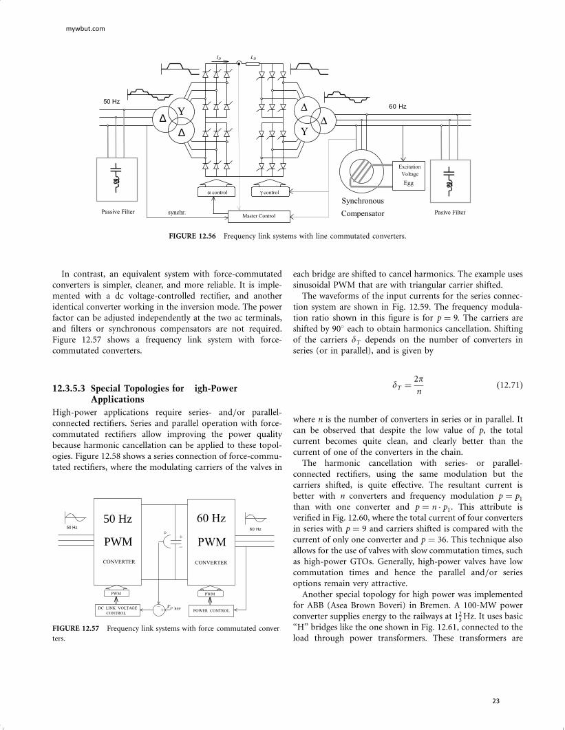
Figure 12.56 shows a typical line-commutated system in which
a 60-Hz load is fed by a 50-Hz supply. As the 60-Hz side needs
excitation to commutate the valves, a synchronous compen-
sator has been required.
iLA
iLB
Lf
I_line(a)
I_line(b)
iLC
ifC
ifBif
A
w
w
w
j
j
j
FIGURE 12.55 Voltage source rectifier with harmonic elimination
capability.
mywbut.com
22
In contrast, an equivalent system with force-commutated
converters is simpler, cleaner, and more reliable. It is imple-
mented with a dc voltage-controlled rectifier, and another
identical converter working in the inversion mode. The power
factor can be adjusted independently at the two ac terminals,
and filters or synchronous compensators are not required.
Figure 12.57 shows a frequency link system with force-
commutated converters.
12.3.5.3 Special Topologies for igh-PowerApplications
High-power applications require series- and=or parallel-
connected rectifiers. Series and parallel operation with force-
commutated rectifiers allow improving the power quality
because harmonic cancellation can be applied to these topol-
ogies. Figure 12.58 shows a series connection of force-commu-
tated rectifiers, where the modulating carriers of the valves in
each bridge are shifted to cancel harmonics. The example uses
sinusoidal PWM that are with triangular carrier shifted.
The waveforms of the input currents for the series connec-
tion system are shown in Fig. 12.59. The frequency modula-
tion ratio shown in this figure is for p ¼ 9. The carriers are
shifted by 90� each to obtain harmonics cancellation. Shifting
of the carriers dT depends on the number of converters in
series (or in parallel), and is given by
dT ¼2pn
ð12:71Þ
where n is the number of converters in series or in parallel. It
can be observed that despite the low value of p, the total
current becomes quite clean, and clearly better than the
current of one of the converters in the chain.
The harmonic cancellation with series- or parallel-
connected rectifiers, using the same modulation but the
carriers shifted, is quite effective. The resultant current is
better with n converters and frequency modulation p ¼ p1
than with one converter and p ¼ n � p1. This attribute is
verified in Fig. 12.60, where the total current of four converters
in series with p ¼ 9 and carriers shifted is compared with the
current of only one converter and p ¼ 36. This technique also
allows for the use of valves with slow commutation times, such
as high-power GTOs. Generally, high-power valves have low
commutation times and hence the parallel and=or series
options remain very attractive.
Another special topology for high power was implemented
for ABB (Asea Brown Boveri) in Bremen. A 100-MW power
converter supplies energy to the railways at 123
Hz. It uses basic
‘‘H’’ bridges like the one shown in Fig. 12.61, connected to the
load through power transformers. These transformers are
∆∆
Y50 Hz
LDID
FIGURE 12.56 Frequency link systems with line commutated converters.
50 Hz
PWM
50 HzD
FIGURE 12.57 Frequency link systems with force commutated conver
ters.
mywbut.com
23

vMODA vMOD
B
SPWM generation
vMODA vMOD
B
SPWM generation
MAINS SUPPLY
w
w
w
FIGURE 12.58 Series connection system with force commutated rectifiers.
mywbut.com
24

connected in parallel at the converter side, and in series at the
load side.
The system uses SPWM with triangular carriers shifted, and
depending on the number of converters connected in the
chain of bridges, the voltage waveform becomes more and
more sinusoidal. Figure 12.62 shows a back-to-back system
using a chain of 12 ‘‘H’’ converters connected as shown in Fig.
12.61b.
The ac voltage waveform obtained with the topology of Fig.
12.62 is displayed in Fig. 12.63. It can be observed that the
voltage is formed by small steps that depend on the number of
converters in the chain (12 in this case). The current is almost
perfectly sinusoidal.
Figure 12.64 shows the voltage waveforms for different
number of converters connected in the bridge. It is clear
that the larger the number of converters, the better the voltage.
Another interesting result with this converter is that the ac
voltages become modulated by both pulsewidth and ampli-
tude (PWM and AM). This is because when the pulse
modulation changes, the steps of the amplitude change. The
maximum number of steps of the resultant voltage is equal to
the number of converters. When the voltage decreases, some
steps disappear, and then the amplitude modulation becomes
a discrete function. Figure 12.65 shows the amplitude modu-
lation of the voltage.
12.3.5.4 Machine Drives Applications
One of the most important applications of force-commutated
rectifiers is in machine drives. Line-commutated thyristor
converters have limited applications because they need excita-
tion to extinguish the valves. This limitation do not allow the
use of line-commutated converters in induction machine
drives. On the other hand, with force-commutated converters
four-quadrant operation is achievable. Figure 12.66 shows a
typical frequency converter with a force-commutated rectifier-
inverter link. The rectifier side controls the dc link, and the
inverter side controls the machine. The machine can be a
synchronous, brushless dc, or induction machine. The reversal
of both speed and power are possible with this topology. At
the rectifier side, the power factor can be controlled, and even
with an inductive load such as an induction machine, the
source can ‘‘see’’ the load as capacitive or resistive. Changing
the frequency of the inverter controls the machine speed, and
the torque is controlled through the stator currents and torque
angle. The inverter will become a rectifier during regenerative
braking, which is possible by making slip negative in an
induction machine, or by making the torque angle negative
in synchronous and brushless dc machines.
A variation of the drive of Fig. 12.66 is found in electric
traction applications. Battery-powered vehicles use the inver-
ter as a rectifier during regenerative braking, and sometimes
the inverter is also used as a battery charger. In this case, the
rectifier can be fed by a single-phase or by a three-phase
system. Figure 12.67 shows a battery-powered electric bus
system. This system uses the power inverter of the traction
motor as a rectifier for two purposes: regenerative braking;
and as a battery charger fed by a three-phase power source.
12.3.5.5 Variable Speed Power Generation
Power generation at 50 or 60 Hz requires constant speed
machines. In addition, induction machines are not currently
used in power plants because of magnetization problems. With
the use of frequency-link force-commutated converters, vari-
able-speed constant-frequency generation becomes possible,
Total current
FIGURE 12.59 Input currents and carriers of the series connection
system of Fig. 12.58.
FIGURE 12.60 Four converters in series and , compared with one
converter and 36.
+
FIGURE 12.61 The ‘‘H’’ modulator: (a) one bridge; and (b) bridge
connected in series at load side through isolation transformers.
mywbut.com
25

even with induction generators. The power plant in Fig. 12.68
shows a wind generator implemented with an induction
machine, and a rectifier-inverter frequency link connected to
the utility. The dc link voltage is kept constant with the
converter located at the mains side. The converter connected
at the machine side controls the slip of the generator and
adjusts it according to the speed of wind or power require-
ments. The utility is not affected by the power factor of the
generator, because the two converters keep the cosj of the
machine independent of the mains supply. The last one can
even be adjusted to operate at leading power factor.
V IS
FIGURE 12.63 Voltage and current waveforms with 12 converters.
FIGURE 12.64 Voltage waveforms with different numbers of ‘‘H’’
bridges in series.
50 Hz
"H"
"H"
"H"
"H"
"H"
"H"
"H"
"H"
phase "b"
phase "c"
ID1
FIGURE 12.62 Frequency link with force commutated converters and sinusoidal voltage modulation.
mywbut.com
26

Variable-speed constant-frequency generation also can be
used in either hydraulic or thermal plants. This allows for
optimal adjustment of the efficiency-speed characteristics of
the machines. In Japan, wound rotor induction generators
working as variable speed synchronous machines are being
used as constant frequency generators. They operate in
hydraulic plants that are able to store water during low
demand periods. A power converter is connected at the slip
rings of the generator. The rotor is then fed with variable
+
FIGURE 12.66 Frequency converter with force commutated converters.
R V NG - ARG NG
L TRON SW T
S L TOR
TRACTION
MOTOR
FIGURE 12.67 Electric bus system with regenerative braking and battery charger.
FIGURE 12.65 Amplitude modulation of the ‘‘H’’ bridges of Fig. 12.62.
a
V
FIGURE 12.68 Variable speed constant frequency wind generator.
mywbut.com
27

frequency excitation. This allows the generator to generate at
different speeds around the synchronous rotating flux.
mywbut.com
28