Embed Size (px)
Citation preview

ZHANG ET AL. VOL. 7 ’ NO. 7 ’ 6212–6218 ’ 2013
www.acsnano.org
6212
June 05, 2013
C 2013 American Chemical Society
Three-Dimensional NanolithographyUsing Light Scattering from ColloidalParticlesXu A. Zhang, Jonathan Elek, and Chih-Hao Chang*
Department of Mechanical and Aerospace Engineering, North Carolina State University, Raleigh, North Carolina 27695, United States
Three-dimensional (3D) nanostructureshave many inherent advantages, andthey have enabled a number of key
innovations in nanoscience in recent years.For example, high surface area-to-volumeratio of 3D structures can yield more efficientenergy conversion in solar cells1 and ultra-fast battery electrodes.2 Properly designedperiodic 3D nanostructures can be used asphotonic3�5 and phononic6 crystals. Highaspect ratio surface nanostructures can alsolead to bioinspired anti-reflection and self-cleaning surfaces.7,8 In biomedical areas, hol-low nanostructures and nanoparticles havebeen investigated for drug delivery systemsdue to their unique capability to preciselyhold and release drugs.9�13 Various “top-down” 3D lithography approaches have beenused to enable these advances, includinglayer-by-layer techniques,3�5 focused ionbeam milling,14 and electron-beam litho-graphy.15 One particular effective 3D pattern-ing technique that has drawn significant re-search interest is direct-write two-photonpolymerization, which allows patterning ofarbitrary structures in 3D space.16�19 However,
since this is inherently a serial process wherefocused light is scanned across the sampleto expose individual voxels, the write timeincreases significantly for large areas. Thistechnique also requires elaborate systemhardware, including ultrafast pulsed lasers,scanning optics, and feedback control elec-tronics. While these techniques are effectivein creating complex structures, they can becostly and difficult to scale up for manufac-turing. One attractive method for large-areapatterning is phase-shift lithography basedon the Talbot effect,20�24 where a two-dimensional (2D) phase mask is illuminatedto generate a periodic 3D intensity pattern.Thismethod requires a single exposure, result-ing in 3D lithography with high-throughputand scalability. This technique has been de-monstrated to be effective when used in con-junction with phase masks fabricated usingdeep-ultraviolet,21 interference,22 Dip-Pen,23
and electron-beam lithography.24
Among the diverse emerging nanofabri-cation methods, colloidal-based techniquehas also drawn wide attention.25�42 These“bottom-up” techniques exploit colloidal
* Address correspondence [email protected].
Received for review April 29, 2013and accepted June 5, 2013.
Published online10.1021/nn402637a
ABSTRACT The interaction between light and colloidal ele-
ments can result in a wealth of interesting near-field optical
patterns. By examining the optical and colloidal properties, the
intensity distribution can be tailored and harnessed for three-
dimensional nanolithography. Here, we examine the use of light
scattering from colloidal particles to fabricate complex hollow
nanostructures. In this approach, a single colloidal sphere is illuminated to create a scattering pattern, which is captured by a photoresist in close
proximity. No external optical elements are required, and the colloidal elements alone provide the modulation of the optical intensity pattern. The
fabricated nanostructures can be designed to have multiple shells, confined volumes, and single top openings, resembling “nano-volcanoes.” The geometry
of such structures is dependent on the scattered light distribution and can be accurately modeled by examining the light�particle interaction. The hollow
nanostructures can be used to trap nanomaterial, and we demonstrate their ability to trap 50 nm silica nanoparticles. These well-defined surface hollow
structures can be further functionalized for applications in controlled drug delivery and biotrapping. Colloidal elements with different geometries and
material compositions can also be incorporated to examine other light�colloid interactions.
KEYWORDS: nanolithography . three-dimensional nanostructures . colloids . self-assembly . light scattering
ARTIC
LE
ZHANG ET AL. VOL. 7 ’ NO. 7 ’ 6212–6218 ’ 2013
www.acsnano.org
6213
particles as elementary building blocks, where theparticles self-assemble to form 3D structures25�29
or act as physical masks for subsequent additivedeposition30�34,37 or subtractive etching.35�37 Thesetechniques can yield high-quality nanostructures, suchas hemispherical metal caps,34 nanopores,35 and sculp-tured colloids36 with relatively low costs. Recently, wedemonstrated that close-packed colloidal arrays canalso be used as an optical phase mask to fabricateperiodic 3D nanostructures with controllable latticeparameters.38 By harnessing the optical interactionwith colloidal elements, 3D patterning with more de-sign parameters can be enabled by controlling bothoptical and colloidal parameters.In this work, we investigate the use of light scattering
from individual colloidal elements for 3D nanolitho-graphy. In the proposed method, isolated particlefocuses and scatters normal-incident light into multi-ple intensity lobes, which is governed by the scatteringcharacteristics. The intensity pattern can then be re-corded by underlying photosensitive materials, result-ing in 3D hollow shell-like structures. We focus on theMie scattering regime for a spherical particle, where theparticle diameter D is comparable to wavelength λ. In thisregime, the angular-variant scattering profile can result incomplex 3D intensity patterns. No masks are needed inthis approach, and the colloidal elements are assembleddirectly on the photoresist. There has been exciting workutilizing near-field light focusing from individual colloidalparticles for nanolithography,43�45 but they have beenlimited to 2D patterns. This work explores using colloidallight scattering to fabricate 3D geometries. While in thisstudy we focus on dielectric nanospheres, other colloidswith nonspherical geometries35�38 can be incorporatedinto this technique. Metallic nanoparticles can also beutilized to enable localized plasmonic interactions forsubwavelength patterning. The proposed method canalso be utilized for 3D visualization of near-field enhance-ment of plasmonic nanostructures.46 Particle light scatter-ing is awell-knownphenomenonandhistoricallyhasbeenused to determine particle size distribution in colloidalsolutions47 and to study aerosols in the atmosphere,48 butin this work, they are employed for 3D lithography.The proposed method is illustrated in Figure 1,
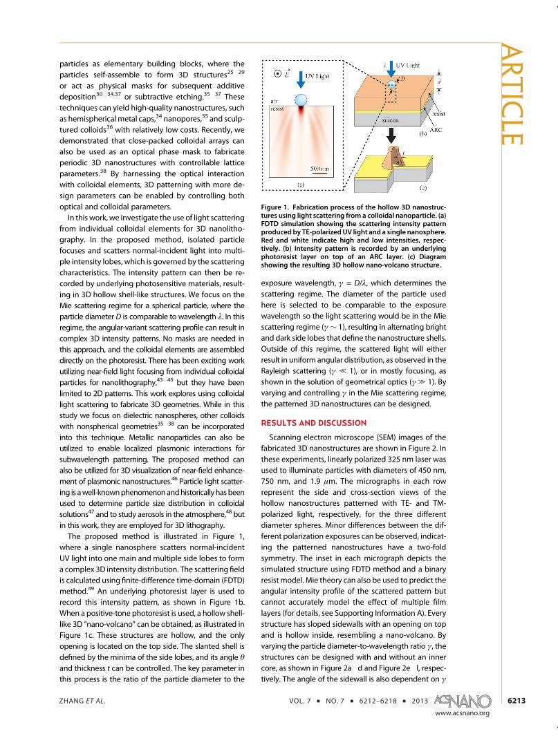
where a single nanosphere scatters normal-incidentUV light into one main and multiple side lobes to forma complex 3D intensity distribution. The scattering fieldis calculated using finite-difference time-domain (FDTD)method.49 An underlying photoresist layer is used torecord this intensity pattern, as shown in Figure 1b.When a positive-tone photoresist is used, a hollow shell-like 3D “nano-volcano” can be obtained, as illustrated inFigure 1c. These structures are hollow, and the onlyopening is located on the top side. The slanted shell isdefined by the minima of the side lobes, and its angle θand thickness t can be controlled. The key parameter inthis process is the ratio of the particle diameter to the
exposure wavelength, γ = D/λ, which determines thescattering regime. The diameter of the particle usedhere is selected to be comparable to the exposurewavelength so the light scattering would be in the Miescattering regime (γ∼ 1), resulting in alternating brightand dark side lobes that define the nanostructure shells.Outside of this regime, the scattered light will eitherresult in uniform angular distribution, as observed in theRayleigh scattering (γ , 1), or in mostly focusing, asshown in the solution of geometrical optics (γ. 1). Byvarying and controlling γ in the Mie scattering regime,the patterned 3D nanostructures can be designed.
RESULTS AND DISCUSSION
Scanning electron microscope (SEM) images of thefabricated 3D nanostructures are shown in Figure 2. Inthese experiments, linearly polarized 325 nm laser wasused to illuminate particles with diameters of 450 nm,750 nm, and 1.9 μm. The micrographs in each rowrepresent the side and cross-section views of thehollow nanostructures patterned with TE- and TM-polarized light, respectively, for the three differentdiameter spheres. Minor differences between the dif-ferent polarization exposures can be observed, indicat-ing the patterned nanostructures have a two-foldsymmetry. The inset in each micrograph depicts thesimulated structure using FDTD method and a binaryresist model. Mie theory can also be used to predict theangular intensity profile of the scattered pattern butcannot accurately model the effect of multiple filmlayers (for details, see Supporting Information A). Everystructure has sloped sidewalls with an opening on topand is hollow inside, resembling a nano-volcano. Byvarying the particle diameter-to-wavelength ratio γ, thestructures can be designed with and without an innercore, as shown in Figure 2a�d and Figure 2e�l, respec-tively. The angle of the sidewall is also dependent on γ
Figure 1. Fabrication process of the hollow 3D nanostruc-tures using light scattering from a colloidal nanoparticle. (a)FDTD simulation showing the scattering intensity patternproduced by TE-polarized UV light and a single nanosphere.Red and white indicate high and low intensities, respec-tively. (b) Intensity pattern is recorded by an underlyingphotoresist layer on top of an ARC layer. (c) Diagramshowing the resulting 3D hollow nano-volcano structure.
ARTIC
LE

ZHANG ET AL. VOL. 7 ’ NO. 7 ’ 6212–6218 ’ 2013
www.acsnano.org
6214
and can be designed to be 67 to 83�. The exposure doseis another factor that affects sidewall thickness and theinner core geometry. We have shown that the sidewallthickness can be controlled down to 60 nm.The colloidal light scattering can be described
using the FDTD and binary resist models developed(Supporting Information A), and the nano-volcanodimensions can be accurately predicted. Figure 3illustrates a quantitative comparison of the patternedand predicted structures using a 1 μm diameter parti-cle and 325 nmwavelength TE-polarized exposure (γ =3.08). The sidewall angles and thicknesses are com-pared, showing good agreement between the experi-ment and simulation. Note that the voids in thesidewall of the simulated cross section are enclosedspaces and cannot bedissolved by the developer in theexperiments, forming a thick solid sidewall. TheseFDTD and binary resist models were used to predictall simulated nano-volcano structures in this work. Therelationships of exposure dose with sidewall angle,sidewall thickness, and the top geometry of thenano-volcanoes are described in more detail in Sup-porting Information B.Since the lithographic exposure is governed by the
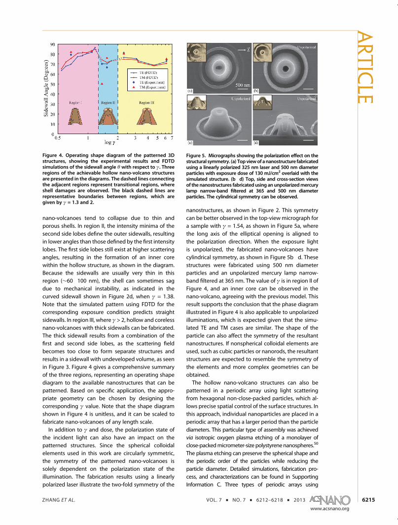
light scattering profile in theMie scattering regime, thefabricated structure can be designed by controllingthe particle diameter-to-wavelength ratio γ. To illus-trate this dependency, the sidewall angles of the nano-volcanoes are compared with respect to differentexposure γ values, as shown in Figure 4. Here thesidewall angle values are experimentally measuredusing cross-section SEM micrographs and comparedwith theoretical predictions using FDTD method.
Based on the values of γ, the geometries of thenano-volcanoes can be divided into three regimes, asrepresented by the colors. In region I, where γ< 1.3, theintensity minima of the first side lobes of the colloidalscattering pattern define the outer sidewall, and thusthe angle increases as γ increases. The structures in thisregion are coreless and have nearly vertical sidewallswhen γ approaches 1.3, which defines the boundary(black dashed line) between regions I and II. Thedashed lines connecting regions I and II representthe transitional region, where 1.2 < γ < 1.4 and the
Figure 2. Micrographs of the fabricated hollow 3D nanostructures using TE- and TM-polarized 325 nm illuminations. The insetdiagrams show the corresponding simulated nanostructures using FDTDmethod and a binary resistmodel. The nanostructures ineach rowwere fabricated under the same conditions: (a�d) particle diameterD = 450 nm, exposure dose = 130mJ/cm2, γ = 1.38;(e�h) D = 750 nm, exposure dose = 120 mJ/cm2, γ = 2.30; (i�l) D = 1.9 1m, exposure dose = 130 mJ/cm2, γ = 5.85.
Figure 3. Structure prediction using FDTD and binary resistmodels for nano-volcano. Diagram (a) and (b) compare theside geometries between the fabricated and simulatedstructures, respectively, while (c) and (d) present a quanti-tative comparison of the same fabricated and simulatednano-volcano interiors, respectively.
ARTIC
LE
ZHANG ET AL. VOL. 7 ’ NO. 7 ’ 6212–6218 ’ 2013
www.acsnano.org
6215
nano-volcanoes tend to collapse due to thin andporous shells. In region II, the intensity minima of thesecond side lobes define the outer sidewalls, resultingin lower angles than those defined by the first intensitylobes. The first side lobes still exist at higher scatteringangles, resulting in the formation of an inner corewithin the hollow structure, as shown in the diagram.Because the sidewalls are usually very thin in thisregion (∼60�100 nm), the shell can sometimes sagdue to mechanical instability, as indicated in thecurved sidewall shown in Figure 2d, when γ = 1.38.Note that the simulated pattern using FDTD for thecorresponding exposure condition predicts straightsidewalls. In region III, where γ > 2, hollow and corelessnano-volcanoes with thick sidewalls can be fabricated.The thick sidewall results from a combination of thefirst and second side lobes, as the scattering fieldbecomes too close to form separate structures andresults in a sidewall with undeveloped volume, as seenin Figure 3. Figure 4 gives a comprehensive summaryof the three regions, representing an operating shapediagram to the available nanostructures that can bepatterned. Based on specific application, the appro-priate geometry can be chosen by designing thecorresponding γ value. Note that the shape diagramshown in Figure 4 is unitless, and it can be scaled tofabricate nano-volcanoes of any length scale.In addition to γ and dose, the polarization state of
the incident light can also have an impact on thepatterned structures. Since the spherical colloidalelements used in this work are circularly symmetric,the symmetry of the patterned nano-volcanoes issolely dependent on the polarization state of theillumination. The fabrication results using a linearlypolarized laser illustrate the two-fold symmetry of the
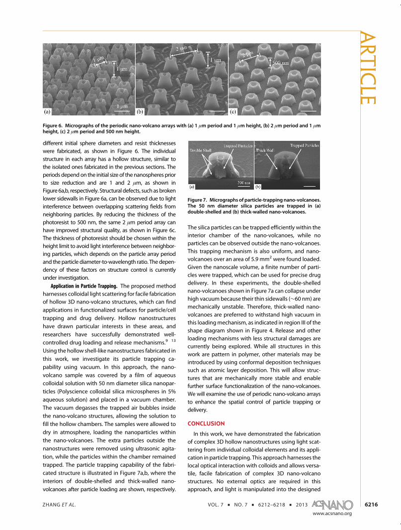
nanostructures, as shown in Figure 2. This symmetrycan be better observed in the top-view micrograph fora sample with γ = 1.54, as shown in Figure 5a, wherethe long axis of the elliptical opening is aligned tothe polarization direction. When the exposure lightis unpolarized, the fabricated nano-volcanoes havecylindrical symmetry, as shown in Figure 5b�d. Thesestructures were fabricated using 500 nm diameterparticles and an unpolarized mercury lamp narrow-band filtered at 365 nm. The value of γ is in region II ofFigure 4, and an inner core can be observed in thenano-volcano, agreeing with the previous model. Thisresult supports the conclusion that the phase diagramillustrated in Figure 4 is also applicable to unpolarizedilluminations, which is expected given that the simu-lated TE and TM cases are similar. The shape of theparticle can also affect the symmetry of the resultantnanostructures. If nonspherical colloidal elements areused, such as cubic particles or nanorods, the resultantstructures are expected to resemble the symmetry ofthe elements and more complex geometries can beobtained.The hollow nano-volcano structures can also be
patterned in a periodic array using light scatteringfrom hexagonal non-close-packed particles, which al-lows precise spatial control of the surface structures. Inthis approach, individual nanoparticles are placed in aperiodic array that has a larger period than the particlediameters. This particular type of assembly was achievedvia isotropic oxygen plasma etching of a monolayer ofclose-packedmicrometer-size polystyrenenanospheres.50
The plasma etching can preserve the spherical shape andthe periodic order of the particles while reducing theparticle diameter. Detailed simulations, fabrication pro-cess, and characterizations can be found in SupportingInformation C. Three types of periodic arrays using
Figure 4. Operating shape diagram of the patterned 3Dstructures, showing the experimental results and FDTDsimulations of the sidewall angle θ with respect to γ. Threeregions of the achievable hollow nano-volcano structuresare presented in the diagrams. The dashed lines connectingthe adjacent regions represent transitional regions, whereshell damages are observed. The black dashed lines arerepresentative boundaries between regions, which aregiven by γ = 1.3 and 2.
Figure 5. Micrographs showing the polarization effect on thestructural symmetry. (a) Topviewof ananostructure fabricatedusing a linearly polarized 325 nm laser and 500 nm diameterparticles with exposure dose of 130 mJ/cm2 overlaid with thesimulated structure. (b�d) Top, side and cross-section viewsof the nanostructures fabricatedusing anunpolarizedmercurylamp narrow-band filtered at 365 and 500 nm diameterparticles. The cylindrical symmetry can be observed.
ARTIC
LE
ZHANG ET AL. VOL. 7 ’ NO. 7 ’ 6212–6218 ’ 2013
www.acsnano.org
6216
different initial sphere diameters and resist thicknesseswere fabricated, as shown in Figure 6. The individualstructure in each array has a hollow structure, similar tothe isolated ones fabricated in the previous sections. Theperiods dependon the initial size of thenanospheres priorto size reduction and are 1 and 2 μm, as shown inFigure 6a,b, respectively. Structural defects, suchasbrokenlower sidewalls in Figure 6a, can be observed due to lightinterference between overlapping scattering fields fromneighboring particles. By reducing the thickness of thephotoresist to 500 nm, the same 2 μm period array canhave improved structural quality, as shown in Figure 6c.The thickness of photoresist should be chosen within theheight limit to avoid light interference between neighbor-ing particles, which depends on the particle array periodand theparticle diameter-to-wavelength ratio. Thedepen-dency of these factors on structure control is currentlyunder investigation.
Application in Particle Trapping. The proposed methodharnesses colloidal light scattering for facile fabricationof hollow 3D nano-volcano structures, which can findapplications in functionalized surfaces for particle/celltrapping and drug delivery. Hollow nanostructureshave drawn particular interests in these areas, andresearchers have successfully demonstrated well-controlled drug loading and release mechanisms.9�13
Using the hollow shell-like nanostructures fabricated inthis work, we investigate its particle trapping ca-pability using vacuum. In this approach, the nano-volcano sample was covered by a film of aqueouscolloidal solution with 50 nm diameter silica nanopar-ticles (Polyscience colloidal silica microspheres in 5%aqueous solution) and placed in a vacuum chamber.The vacuum degasses the trapped air bubbles insidethe nano-volcano structures, allowing the solution tofill the hollow chambers. The samples were allowed todry in atmosphere, loading the nanoparticles withinthe nano-volcanoes. The extra particles outside thenanostructures were removed using ultrasonic agita-tion, while the particles within the chamber remainedtrapped. The particle trapping capability of the fabri-cated structure is illustrated in Figure 7a,b, where theinteriors of double-shelled and thick-walled nano-volcanoes after particle loading are shown, respectively.
The silica particles can be trapped efficiently within theinterior chamber of the nano-volcanoes, while noparticles can be observed outside the nano-volcanoes.This trapping mechanism is also uniform, and nano-volcanoes over an area of 5.9 mm2 were found loaded.Given the nanoscale volume, a finite number of parti-cles were trapped, which can be used for precise drugdelivery. In these experiments, the double-shellednano-volcanoes shown in Figure 7a can collapse underhigh vacuumbecause their thin sidewalls (∼60 nm) aremechanically unstable. Therefore, thick-walled nano-volcanoes are preferred to withstand high vacuum inthis loadingmechanism, as indicated in region III of theshape diagram shown in Figure 4. Release and otherloading mechanisms with less structural damages arecurrently being explored. While all structures in thiswork are pattern in polymer, other materials may beintroduced by using conformal deposition techniquessuch as atomic layer deposition. This will allow struc-tures that are mechanically more stable and enablefurther surface functionalization of the nano-volcanoes.We will examine the use of periodic nano-volcano arraysto enhance the spatial control of particle trapping ordelivery.
CONCLUSION
In this work, we have demonstrated the fabricationof complex 3D hollow nanostructures using light scat-tering from individual colloidal elements and its appli-cation in particle trapping. This approach harnesses thelocal optical interaction with colloids and allows versa-tile, facile fabrication of complex 3D nano-volcanostructures. No external optics are required in thisapproach, and light is manipulated into the designed
Figure 6. Micrographs of the periodic nano-volcano arrays with (a) 1 μm period and 1 μm height, (b) 2 μm period and 1 μmheight, (c) 2 μm period and 500 nm height.
Figure 7. Micrographs of particle-trapping nano-volcanoes.The 50 nm diameter silica particles are trapped in (a)double-shelled and (b) thick-walled nano-volcanoes.
ARTIC
LE

ZHANG ET AL. VOL. 7 ’ NO. 7 ’ 6212–6218 ’ 2013
www.acsnano.org
6217
optical pattern solely by the colloids. The scatteringfield is well described by the proposed shape diagram,and various geometries can be readily fabricatedby controlling the particle size-to-wavelength ratio.The 3D nanostructures can also be patterned withperiodic order using non-close-packed colloidal as-sembly, allowing precise spatial control for particletrapping/delivery. The nanoscale interior volume ofthe hollow nano-volcano structures has been shownto be effective in trapping nanoparticles and can
potentially be used as functionalized patches forparticle/cell trapping and precise drug delivery. Otherpossible applications involve biosensing and opticalor acoustic focusing using the tapered sidewalls.Although in this work we focused on readily availablespherical nanoparticles as scattering objects, othertypes of colloidal elements, such as cubic, tetrahedral,and rod particles, can be incorporated into thisapproach to enable a wide variety of achievable 3Dnanostructures.
METHODSSample Preparation. In all experiments, the samples were
prepared on silicon substrates. A layer of anti-reflection coating(ARC i-CON-16, Brewer Science, Inc.) was used to reduce backreflection. The anti-reflection coating is designed to reduceback reflection from the resist and ARC interface, and itsthickness is optimized to minimize normal-incident light. TheARC thickness is around 90 and 160 nm for the 325 and 365 nmwavelengthexposures, respectively. Positivephotoresist (SumitomoPFi88A7) was spin-coated on the ARC layer. The thickness of thephotoresist layer should be thick enough to capture the scatteringpattern and depends on the choice of particle size. However, thethickness is limited by the absorption of the photoresist material,as light intensity decays exponentially into thematerial. A range of0.5 to 1.5 μm thickness was used for the particle size range used inour experiments. To enhance sphere adhesion and facilitate thespreading of the aqueous colloidal solution, a 10 nm thick layer ofsilicon dioxide was deposited on top of the resist surface usingelectron-beam evaporation. It is designed to be thin enough tohave minimal optical effects on the scattering pattern. Monodis-persedpolystyrene sphereswithvariousdiameters from350nmto1.9 μm (Polyscience Polybead Microspheres in 2.5% aqueoussolution) were used as scattering objects in the experiments. Thesolution was spin-coated on the prepared sample to assembleisolated nanospheres.
Lithographic exposures were performed using either alinearly polarized 325 nm He�Cd laser or an unpolarized mercurylamp narrow-band filtered at 365 nm. After exposing the sampleswithdoses of 100�200mJ/cm2, thenanosphereswere removedbyultrasonic agitation and the thin silicon dioxide layer was etchedusingbufferedHF (J.T. Baker, bufferedoxideetch10:1). Theexposedsamples were then developed in 2.4% tetramethylammoniumhydroxide (TMAH) developer solution (Microposit MF-CD-26) for1�2min. The sampleswere characterizedusing topviewandcross-section view scanning electron microscope (JEOL 6400F) at 5 keV.
Simulation andModeling. The colloidal light scattering intensitydistribution in the photoresist was modeled using finite-differencetime-domain (FDTD)methods. The resultswerealso comparedwiththe results from the analytical Mie scattering solutions, as describedin Supporting Information A. A binary photoresist model was usedto predict the resulting structures, where any volume above athreshold dose was completely removed. The intensity profilethrough the thickness of the resist was assumed to have anexponential decay to model the resist absorption. The geometriesof the simulated structures are then quantitatively analyzed inMatlab. The predicted models are depicted as inset diagrams withtheir corresponding fabrication results.
Conflict of Interest: The authors declare no competingfinancial interest.
Acknowledgment. We gratefully acknowledge the students,staff, and facility support from the North Carolina State UniversityNanofabrication Facility (NNF). Thisworkwas supportedbyaNASAOffice of the Chief Technologist's Space Technology ResearchOpportunity�Early Career Faculty grant (Grant NNX12AQ46G)and by the National Science Foundation (Grant EEC-1160483)through the Nanosystems Engineering Research Center for
Advanced Self-Powered Systems of Integrated Sensors and Tech-nologies (ASSIST).
Supporting Information Available: Additional information ontheoretical structure prediction, exposure dose dependency ofnano-volcano geometry, and fabrication of periodic nano-volcano arrays. This material is available free of charge viathe Internet at http://pubs.acs.org.
REFERENCES AND NOTES1. Fan, Z.; Razavi, H.; Do, J.; Moriwaki, A.; Ergen, O.; Chueh, Y.-L.;
Leu, P. W.; Ho, J. C.; Takahashi, T.; Reichertz, L. A.; et al. Three-Dimensional Nanopillar-Array Photovoltaics on Low-Costand Flexible Substrates. Nat. Mater. 2009, 8, 648–653.
2. Zhang, H.; Yu, X.; Braun, P. V. Three-Dimensional Bicontin-uous Ultrafast-Charge and -Discharge Bulk Battery Elec-trodes. Nat. Nanotechnol. 2011, 6, 277–281.
3. Lin, S. Y.; Fleming, J. G.; Hetherington, D. L.; Smith, B. K.;Biswas, R.; Ho, K. M.; Sigalas, M. M.; Zubrzycki, W.; Kurtz,S. R.; Bur, J. A Three-Dimensional Photonic Crystal Operat-ing at Infrared Wavelengths. Nature 1998, 394, 251–253.
4. Noda, S.; Tomoda, K.; Yamamoto, N.; Chutinan, A. FullThree-Dimensional Photonic Bandgap Crystals at Near-Infrared Wavelengths. Science 2000, 289, 604–606.
5. Qi, M.; Lidorikis, E.; Rakich, P. T.; Johnson, S. G.; Joannopoulos,J. D.; Ippen, E. P.; Smith, H. I. A Three-Dimensional OpticalPhotonic Crystal with Designed Point Defects. Nature 2004,429, 538–542.
6. Jang, J.-H.; Ullal, C. K.; Gorishnyy, T.; Tsukruk, V. V.; Thomas,E. L. Mechanically Tunable Three-Dimensional ElastomericNetwork/Air Structures via Interference Lithography.NanoLett. 2006, 6, 740–743.
7. Min, W.-L.; Jiang, B.; Jiang, P. Bioinspired Self-CleaningAntireflection Coatings. Adv. Mater. 2008, 20, 3914–3918.
8. Park, K.-C.; Choi, H. J.; Chang, C.-H.; Cohen, R. E.; McKinley,G. H.; Barbastathis, G. Nanotextured Silica Surfaces withRobust Superhydrophobicity and Omnidirectional Broad-band Supertransmissivity. ACS Nano 2012, 6, 3789–3799.
9. Li, Z.-Z.; Wen, L.-X.; Shao, L.; Chen, J.-F. Fabrication of PorousHollow Silica Nanoparticles and Their Applications in DrugRelease Control. J. Controlled Release 2004, 98, 245–254.
10. Lou, X.W.; Archer, L. A.; Yang, Z. HollowMicro-/Nanostructures:Synthesis and Applications. Adv. Mater. 2008, 20, 3987–4019.
11. Yavuz, M. S.; Cheng, Y.; Chen, J.; Cobley, C. M.; Zhang, Q.;Rycenga,M.; Xie, J.; Kim, C.; Song, K. H.; Schwartz, A. G.; et al.Gold Nanocages Covered by Smart Polymers for Con-trolled Release with Near-Infrared Light. Nat. Mater.2009, 8, 935–939.
12. Moon, G. D.; Choi, S.-W.; Cai, X.; Li, W.; Cho, E. C.; Jeong, U.;Wang, L. V.; Xia, Y. A New Theranostic System Based onGoldNanocages and Phase-ChangeMaterials with UniqueFeatures for Photoacoustic Imaging and Controlled Re-lease. J. Am. Chem. Soc. 2011, 133, 4762–4765.
13. Tao, S. L.; Desai, T. A. Microfabricated Drug DeliverySystems: From Particles to Pores. Adv. Drug Delivery Rev.2003, 55, 315–328.
ARTIC
LE

ZHANG ET AL. VOL. 7 ’ NO. 7 ’ 6212–6218 ’ 2013
www.acsnano.org
6218
14. Jeon, J.; Floresca, H. C.; Kim, M. J. Fabrication of ComplexThree-Dimensional Nanostructures Using Focused IonBeam and Nanomanipulation. J. Vac. Sci. Technol., B2010, 28, 549–553.
15. Yamazaki, K.; Yamaguchi, H. Three-Dimensional Alignmentwith 10 nm Order Accuracy in Electron-Beam Lithographyon Rotated Sample for Three-Dimensional Nanofabrication.J. Vac. Sci. Technol., B 2008, 26, 2529–2533.
16. Maruo, S.; Nakamura, O.; Kawata, S. Three-DimensionalMicrofabrication with Two-Photon-Absorbed Photopoly-merization. Opt. Lett. 1997, 22, 132–134.
17. Cumpston, B. H.; Ananthavel, S. P.; Barlow, S.; Dyer, D. L.;Ehrlich, J. E.; Erskine, L. L.; Heikal, A. A.; Kuebler, S. M.; Lee,I.-Y. S.; McCord-Maughon, D.; et al. Two-Photon Polymer-ization Initiators for Three-Dimensional Optical DataStorage and Microfabrication. Nature 1999, 398, 51–54.
18. Kawata, S.; Sun, H.-B.; Tanaka, T.; Takada, K. Finer Featuresfor Functional Microdevices. Nature 2001, 412, 697–698.
19. Haske, W.; Chen, V. W.; Hales, J. M.; Dong, W.; Barlow, S.;Marder, S. R.; Perry, J. W. 65 nm Feature Sizes Using VisibleWavelength 3-D Multiphoton Lithography. Opt. Express2007, 15, 3426–3436.
20. Shir, D.; Nelson, E. C.; Chen, Y. C.; Brzezinski, A.; Liao, H.;Braun, P. V.; Wiltzius, P.; Bogart, K. H. A.; Rogers, J. A. ThreeDimensional Silicon Photonic Crystals Fabricated by TwoPhoton PhaseMask Lithography. Appl. Phys. Lett. 2009, 94,011101-1–011101-3.
21. Jeon, S.; Park, J.-U.; Cirelli, R.; Yang, S.; Heitzman, C. E.;Braun, P. V.; Kenis, P. J. A.; Rogers, J. A. Fabricating ComplexThree-Dimensional Nanostructures with High-ResolutionConformable Phase Masks. Proc. Natl. Acad. Sci. U.S.A.2004, 101, 12428–12433.
22. Jang, J.-H.; Ullal, C. K.; Maldovan, M.; Gorishnyy, T.; Kooi, S.;Koh, C.; Thomas, E. L. 3D Micro- and Nanostructures viaInterference Lithography. Adv. Funct. Mater. 2007, 17,3027–3041.
23. Jang, J.-W.; Zheng, Z.; Lee, O.-S.; Shim, W.; Zheng, G.;Schatz, G. C.; Mirkin, C. A. Arrays of Nanoscale Lenses forSubwavelength Optical Lithography. Nano Lett. 2010, 10,4399–4404.
24. Isoyan, A.; Jiang, F.; Cheng, Y. C.; Cerrina, F.; Wachulak, P.;Urbanski, L.; Rocca, J.; Menoni, C.; Marconi, M. TalbotLithography: Self-Imaging of Complex Structures. J. Vac.Sci. Technol., B 2009, 27, 2931–2937.
25. Blaaderen, A.; van Ruel, R.; Wiltzius, P. Template-DirectedColloidal Crystallization. Nature 1997, 385, 321–324.
26. Gates, B.; Qin, D.; Xia, Y. Assembly of Nanoparticles intoOpaline Structures over Large Areas. Adv. Mater. 1999, 11,466–469.
27. Rycenga, M.; Camargo, P. H. C.; Xia, Y. Template-AssistedSelf-Assembly: A Versatile Approach to Complex Micro-and Nanostructures. Soft Matter 2009, 5, 1129–1136.
28. Xia, Y.; Gates, B.; Yin, Y.; Lu, Y. Monodispersed ColloidalSpheres: Old Materials with New Applications. Adv. Mater.2000, 12, 693–713.
29. Dinsmore, A. D.; Hsu, M. F.; Nikolaides, M. G.; Marquez, M.;Bausch, A. R.; Weitz, D. A. Colloidosomes: SelectivelyPermeable Capsules Composed of Colloidal Particles.Science 2002, 298, 1006–1009.
30. Hulteen, J. C.; Van Duyne, R. P. Nanosphere Lithography: AMaterials General Fabrication Process for Periodic ParticleArray Surfaces. J. Vac. Sci. Technol., A 1995, 13, 1553–1558.
31. Haginoya, C.; Ishibashi, M. Nanostructure Array Fabricationwith a Size-Controllable Natural Lithography. Appl. Phys.Lett. 1997, 71, 2934.
32. Rybczynski, J.; Ebels, U.; Giersig, M. Large-Scale, 2D Arraysof Magnetic Nanoparticles. Colloids Surf., A 2003, 219, 1–6.
33. Velev, O. D.; Tessier, P. M.; Lenhoff, A. M.; Kaler, E. W.Materials: A Class of Porous Metallic Nanostructures. Nat-ure 1999, 401, 548–548.
34. Love, J. C.; Gates, B.D.;Wolfe,D. B.; Paul, K. E.;Whitesides,G.M.Fabrication and Wetting Properties of Metallic Half-Shellswith Submicron Diameters. Nano Lett. 2002, 2, 891–894.
35. Moon, J. H.; Kim, W. S.; Ha, J.-W.; Jang, S. G.; Yang, S.-M.;Park, J.-K. Colloidal Lithography with Crosslinkable
Particles: Fabrication of Hierarchical Nanopore Arrays.Chem. Commun. 2005, 4107–4109.
36. Choi, D.-G.; Jang, S. G.; Kim, S.; Lee, E.; Han, C.-S.; Yang, S.-M.Multifaceted andNanobored Particle Arrays SculptedUsingColloidal Lithography. Adv. Funct. Mater. 2006, 16, 33–40.
37. Yang, S.-M.; Jang, S. G.; Choi, D.-G.; Kim, S.; Yu, H. K.Nanomachining by Colloidal Lithography. Small 2006, 2,458–475.
38. Chang, C.-H.; Tian, L.; Hesse, W. R.; Gao, H.; Choi, H. J.; Kim,J.-G.; Siddiqui, M.; Barbastathis, G. From Two-DimensionalColloidal Self-Assembly to Three-Dimensional Nanolitho-graphy. Nano Lett. 2011, 11, 2533–2537.
39. Sun, Y.; Xia, Y. Shape-Controlled Synthesis of Gold andSilver Nanoparticles. Science 2002, 298, 2176–2179.
40. Xia, Y.; Xiong, Y.; Lim, B.; Skrabalak, S. E. Shape-ControlledSynthesis of Metal Nanocrystals: Simple Chemistry MeetsComplex Physics? Angew. Chem., Int. Ed. 2009, 48, 60–103.
41. Henzie, J.; Grünwald, M.; Widmer-Cooper, A.; Geissler, P. L.;Yang, P. Self-Assembly of Uniform Polyhedral Silver Nano-crystals into Densest Packings and Exotic Superlattices.Nat. Mater. 2012, 11, 131–137.
42. Biacchi, A. J.; Schaak, R. E. The Solvent Matters: Kineticversus Thermodynamic Shape Control in the Polyol Synthe-sis of RhodiumNanoparticles.ACSNano 2011, 5, 8089–8099.
43. Devilez, A.; Bonod, N.; Wenger, J.; Gérard, D.; Stout, B.;Rigneault, H.; Popov, E. Three-Dimensional Subwave-length Confinement of Light with Dielectric Microspheres.Opt. Express 2009, 17, 2089–2094.
44. Kühler, P.; García de Abajo, F. J.; Solis, J.; Mosbacher, M.;Leiderer, P.; Afonso, C. N.; Siegel, J. Imprinting the OpticalNear Field of Microstructures with Nanometer Resolution.Small 2009, 5, 1825–1829.
45. Mcleod, E.; Arnold, C. B. Subwavelength Direct-WriteNanopatterning Using Optically Trapped Microspheres.Nat. Nanotechnol. 2008, 3, 413–417.
46. Geldhauser, T.; Kolloch, A.; Murazawa, N.; Ueno, K.; Boneberg,J.; Leiderer, P.; Scheer, E.; Misawa, H. Quantitative Measure-ment of the Near-Field Enhancement of Nanostructures byTwo-Photon Polymerization. Langmuir 2012, 28, 9041–9046.
47. McConnell, M. L. Particle Size Determination by Quasie-lastic Light Scattering. Anal. Chem. 1981, 53, 1007A–1018A.
48. Menzies, R. T.; Kavaya, M. J.; Flamant, P. H.; Haner, D. A.Atmospheric Aerosol Backscatter Measurements Using aTunable Coherent CO2 Lidar. Appl. Opt. 1984, 23, 2510–2517.
49. Oskooi, A. F.; Roundy,D.; Ibanescu,M.; Bermel, P.; Joannopoulos,J. D.; Johnson, S. G. Meep: A Flexible Free-SoftwarePackage for Electromagnetic Simulations by the FDTDMethod. Comput. Phys. Commun. 2010, 181, 687–702.
50. Plettl, A.; Enderle, F.; Saitner, M.; Manzke, A.; Pfahler, C.;Wiedemann, S.; Ziemann, P. Non-Close-Packed Crystalsfrom Self-Assembled Polystyrene Spheres by IsotropicPlasma Etching: Adding Flexibility to Colloid Lithography.Adv. Funct. Mater. 2009, 19, 3279–3284.
ARTIC
LE