Embed Size (px)
Citation preview

ECE505Fall 07Nanolithography and nanopatterning
Modify the surface of a material by patterning the surface:
• in the fabrication of integrated circuits (IC),
• information storage devices
• fabrication of micro-electromechanical systems (MEMS)
• minute sensors
• nano and microfluidic devices
• biochips
• photonics
Depending on the application the nanopatterningtechnique can vary and many times different techniques must be applied in series to achieve the required final product.
One critical parameter is the minimum feature size that determines the particular capability of the chosen technique to print nanometer size devices.

ECE505Fall 07
Photolithography is probably the most well established technique. It is the main technology used by the microelectronics industry. Other approaches:
•“direct writing” on a surface (with or without the addition of material).
Nanolithography and nanopatterning
stylus
E beam writing

ECE505Fall 07Nanolithography and nanopatterning
Electrodewriting
Magneticwriting
Focused energetic beam of particles provides other means to generate patterns in the surface of a resist material. These techniques has extremely high spatial resolution. Electron beam lithography has been the standard method to print arbitrary motives with nanometer size features. Writing with an electric field consists in the modification of the surface by a localized electric current. The changes induced in the surface can derive from the current itselfWriting and reading with a magnetic field is central to the information storage technology.

ECE505Fall 07Nanolithography and nanopatterning
Nanolithography was the driver in the microelectronics industry to maintain the Moore’s Law. An empirical observation made in 1965 by Gordon E. Moore: “number of transistors on an integrated circuit doubles every 24 months.”Nanolithography refers to the technique that allows to define patterns in a surface at ever decreasing length scales.

ECE505Fall 07Nanolithography and nanopatterning
The most prevalent approach employs the exposure of resist materials which are most usually polymeric by energetic photons and particles.
The exposed areas will undergo structural or chemical modification such that they will have a differential solubility in the “developing” solution with respect to the unexposed areas.
The exposed regions may reduce or increase the solubility and that is referred as “negative “ and “positive” resists.
This layer of resist applied on the surface of sample will cover specific regions that will be “protected” in the further processing of the sample for example by chemical etching, or other processing techniques to fabricate surface structures with the size determined by the initial lithographic step. Exposing
radiation
mask
substrate
Thin film
Positive Negative
ECE505Fall 07Nanolithography and nanopatterning
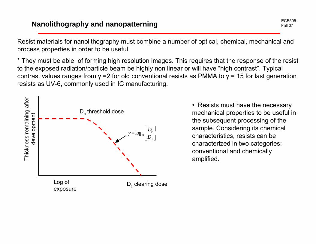
Resist materials for nanolithography must combine a number of optical, chemical, mechanical and process properties in order to be useful.
* They must be able of forming high resolution images. This requires that the response of the resist to the exposed radiation/particle beam be highly non linear or will have “high contrast”. Typical contrast values ranges from γ =2 for old conventional resists as PMMA to γ = 15 for last generation resists as UV-6, commonly used in IC manufacturing.
Thic
knes
s re
mai
ning
afte
r de
velo
pmen
t
Log of exposure
Dc clearing dose
Do threshold dose
010log
C
DD
γ⎡ ⎤
= ⎢ ⎥⎣ ⎦
• Resists must have the necessary mechanical properties to be useful in the subsequent processing of the sample. Considering its chemical characteristics, resists can be characterized in two categories: conventional and chemically amplified.

ECE505Fall 07Nanolithography and nanopatterning
Conventional photoresists: the energy of the radiation in the exposure directly converts into a chemical reaction in the resist.Amplified: an intermediate catalytic process happens prior to development.
Polymethylmethacralate (PMMA) is a positive tone resist that can be activated with UV light, X-rays, electrons or ions. Molecular weights form 500k to 1000 k with slightly different properties, has low contrast γ < 3. In IC fabrication, the most common used resist is diazonapthoquinones (DNQ). It uses a resin mixed with a photoactive compound. Upon exposure the compound is converted to soluble acid allowing the exposed areas to be removed in the development. Typical exposure doses are in the range of 0.1 J cm-2. This resist presents a moderate contrast γ = 6.
Chemical amplified resists also use a polymer backbone. A photo-acid compound is added that will change to an acid after irradiation. Also in the polymer a dissolution inhibitor is added. The acid generated in the exposure reacts with the dissolution inhibitors groups and makes the polymer soluble in the developing solution. The acid acts as a catalytic agent so that the polymer is rendered soluble and the acid is free to move to other locations in the polymer backbone rendering soluble other sites in the polymer chain. In this way the acid compound can react with many sites (up to 100) in the polymer chain and an amplified effect is obtained. Using these resists the dose can be reduced to 5 mJ cm-2.

ECE505Fall 07Photon based nanolithography
Contact and proximity photolithography
In contact photolithography the mask is located in contact with the photoresist. This method allows very good resolution but has few main complications.
•After exposure the mask should be separated from the photoresist and in this process defects can be produces in the printed pattern.
•Also part residues of the resist can remain in the surface of the mask that has to be cleaned after each exposure with the consequent probably degradation of the mask quality.
•These residues of dust particles can be attached to the mask surface not allowing a perfect contact between the mask and the photoresist and consequently degrading the printing.

ECE505Fall 07Photon based nanolithography
Proximity printing: A small gap between the mask and the sample. This small gap reduces the problems that generate dust and contaminants in contact photolithography.
The resolution achievable is limited by diffraction of the light in the features of the mask. In this case diffraction patterns are considered as near field diffraction or Fresnel diffraction. The minimum printable feature size is
minW gλ≈
Projection photolithography
….
The image resolution is limited by diffraction but in this case the image plane is far away from the masks. The far field or Fraunhofferdiffraction models apply in this case. The resolution the simple analysis that is used is Rayleighcriterion is
1.22 fDdλ
=
1.22 1.22 0.61 0.612 sin sin
f fRd f NAλ λ λ λ
α α= = = =

ECE505Fall 07Photon based nanolithography
The resolution of the system however it is more common to write in terms of a constant k1
1R kNAλ
=
Equation above has three parameters that can be manipulated in order to increase the spatial resolution: decrease the empirical constant k1, illuminate with shorter wavelengths and increase the numerical aperture of the system.
The illumination wavelengths used have been picked based on the availability of efficient sources. Hg arc lamps spectrally filtered to narrow the bandwidth to optimize the optical system to a given wavelength and reach the diffraction limit. Lenses can be compensated at determined wavelengths, this is compensated in the primary aberrations (spherical and chromatic). Hg arc lamps produce strong emission at 435 and 365 nm.
Laser based sources are now used. KrF excimer laser emits strongly at 248 nm. Changing the gas to ArF it is possible to produce light at 193 nm and with F2 down to 157 nm. At these wavelengths the materials used in the optical systems start to be a problem.

ECE505Fall 07Photon based nanolithography

ECE505Fall 07Photon based nanolithography
ECE505Fall 07Photon based nanolithography
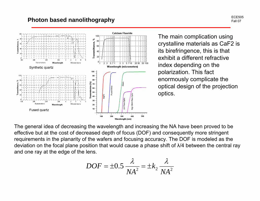
The main complication using crystalline materials as CaF2 is its birefringence, this is that exhibit a different refractive index depending on the polarization. This fact enormously complicate the optical design of the projection optics.
The general idea of decreasing the wavelength and increasing the NA have been proved to be effective but at the cost of decreased depth of focus (DOF) and consequently more stringent requirements in the planarity of the wafers and focusing accuracy. The DOF is modeled as the deviation on the focal plane position that would cause a phase shift of λ/4 between the central ray and one ray at the edge of the lens.
22 20.5DOF kNA NAλ λ
= ± = ±

ECE505Fall 07Photon based nanolithography: EUV lithography
http://www.llnl.gov/str/Sween.html

ECE505Fall 07
Reflective optics
High quality multilayers
Printable defects
At wavelength inspection
EUV sources
Photon based nanolithography: EUV lithography
http://www.llnl.gov/str/Sween.html

ECE505Fall 07Replication of patterns
Replication with a master
Replication methods are referred as “soft lithographies” because they rely in a soft elastomer to achieve intimate conformal contact between the master and the sample.Advantages:
* patterning of curved surfaces* the use of materials that are incompatible with photoresists or developers* large area fabrication.
Schemes A) embossing with a rigid master, B) replica molding with a liquid pre-polymer, C) micro-contact printing with a stamp and D) microfluidic patterning.
ADeformable material
BLiquidprepolymer
Polymer replica
cure
Inked stamp
C
Micro fluidic network
D
Deposit
Ink

ECE505Fall 07Edge lithography
In this technique the edges of a structure become the feature in the resulting pattern. Near field phase shifting photolithography is a contact lithography but includes a mask made out an elastomer to achieve a better contact with the photoresist. The maskinduce phase shifts in the illumination that produces in the surface of the photoresist an interference pattern.
ECE505Fall 07Three dimensional patterning
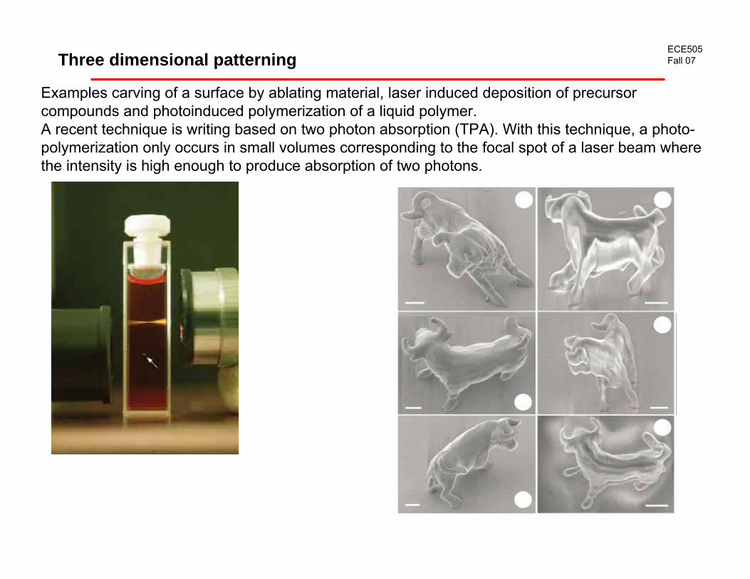
Examples carving of a surface by ablating material, laser induced deposition of precursor compounds and photoinduced polymerization of a liquid polymer. A recent technique is writing based on two photon absorption (TPA). With this technique, a photo-polymerization only occurs in small volumes corresponding to the focal spot of a laser beam where the intensity is high enough to produce absorption of two photons.

ECE505Fall 07Holographic patterning and interferometric lithography
This is a method that uses the interference of two or more beams to activate the surface of the photoresist. This maskless photo-lithographic technique is based on the activation of a photoresistby the interference pattern generated by two or more spatially coherent light beams.

ECE505Fall 07Holographic patterning and interferometric lithography

ECE505Fall 07Self Assembly
This is a “bottom-up” approach. The final structure is achieved when the ensemble of the building blocks reaches its minimum free energy state in which the attraction and repulsion interactions between the components in the surface are well balanced. The building blocks can be divided in three categories depending on its size: molecular self assembly, nanoscale particles (such as colloidal particles) and meso to macro scale dimension objects. In the first category the interaction forces are based on electrostatic, hydrophobic or Van der Waalsinteractions, etc.. In the second a third categories, the organized assembly of blocks rely on external forces as gravity, electric or magnetic fields.

ECE505Fall 07Self Assembly
Phase-separated block copolymersBlock copolymers consists of two or more immiscible polymer fragments jointed by a covalent bond. It can auto-arrange in large domains which typical size depends on the preparation of the sample and on the characteristics of the particular polymers used.
Nano-sphere lithographyThis method uses a monodispersed spherical colloid that are assembled on a surface into a form of a closed packed monolayer with hexagonal symmetry. This monolayer can serve as a mask for subsequent processing of the surface.
v vv vv v
v vv v
v


