Embed Size (px)
Citation preview
Third Place Best Paper (PM11)
eMET POC: Realization of a proof-of-concept 50 keV electron multibeam Mask Exposure ToolElmar Platzgummer, Christof Klein, and Hans Loeschner, IMS Nanofabrication AG, Schreygasse 3, A-1020 Vienna, Austria
ABSTRACTBased on a massively parallel beam writing strategy (BACUS 2010) a mask writer proof-of-concept tool was realized in 2011. The eMET (electron Mask Exposure Tool) POC column is designed to provide ca. 262-thousand (512 x 512) programmable beams of 50 keV energy and 20 nm or 10 nm beam size. The total beam current through the column is up to 1 µA. The eMET POC is equipped with a laser-interferometer controlled stage for exposure of one cm2 test pattern fields on 6” mask blanks. Operating the eMET POC with a stencil plate, first exposure results are presented. The further eMET POC project plan and the roadmap for eMET Alpha, Beta and multi-generational HVM tools are outlined.
Continues on page 3.
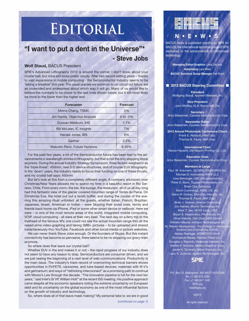
Figure 2. In-situ change of beam size [2]Right-lower Corner.
PhotomaskPhotomaskBACUS—The international technical group of SPIE dedicated to the advancement of photomask technology.
Industry BrIefs—see page 9
CalendarFor a list of meetings —see page 10
N • E • W • S
Take A Look Inside:
February 2012 Volume 28, Issue 2
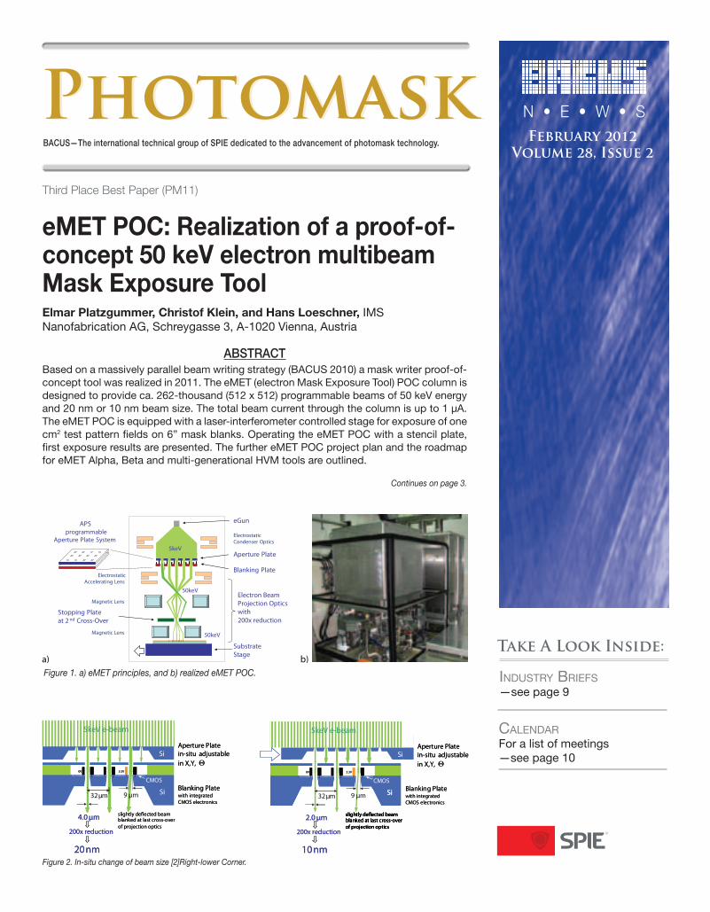
Figure 1. a) eMET principles, and b) realized eMET POC.
BACUS News is published monthly by SPIE for BACUS, the international technical group of SPIE dedicated to the advancement of photomask technology.
Managing Editor/Graphics Linda DeLano
Advertising Lara Miles
BACUS Technical Group Manager Pat Wight
■ 2012 BACUS Steering Committee ■
President Wolfgang Staud, Applied Materials, Inc.
Vice-PresidentJohn Whittey, KLA-Tencor MIE Div.
Secretary Artur Balasinski, Cypress Semiconductor Corp.
Newsletter Editor Artur Balasinski, Cypress Semiconductor Corp.
2012 Annual Photomask Conference ChairsFrank E. Abboud, Intel Corp. Thomas B. Faure, IBM Corp.
International Chair Naoya Hayashi, Dai Nippon Printing Co., Ltd.
Education ChairArtur Balasinski, Cypress Semiconductor Corp.
Members at LargePaul W. Ackmann, GLOBALFOUNDRIES Inc.
Michael D. Archuletta, RAVE LLC Uwe Behringer, UBC Microelectronics
Peter D. Buck, Toppan Photomasks, Inc. Brian Cha, Samsung
Kevin Cummings, ASML US, Inc.Glenn R. Dickey, Shin-Etsu MicroSi, Inc.
Thomas B. Faure, IBM Corp.Brian J. Grenon, Grenon Consulting Jon Haines, Micron Technology Inc.
Mark T. Jee, HOYA Corp, USA Bryan S. Kasprowicz, Photronics, Inc. Oliver Kienzle, Carl Zeiss SMS GmbH
Wilhelm Maurer, Infineon Technologies AGM. Warren Montgomery, The College of Nanoscale
Science and Engineering (CNSE)Abbas Rastegar, SEMATECH North
Emmanuel Rausa, Plasma-Therm LLC. Douglas J. Resnick, Molecular Imprints, Inc. Steffen F. Schulze, Mentor Graphics Corp.
Jacek K. Tyminski, Nikon Precision Inc.Larry S. Zurbrick, Agilent Technologies, Inc.
P.O. Box 10, Bellingham, WA 98227-0010 USATel: +1 360 676 3290Fax: +1 360 647 1445
©2012
All rights reserved.
N • E • W • SEditorial
“I want to put a dent in the Universe”* - Steve Jobs
Wolf Staud, BACUS PresidentSPIE’s Advanced Lithography 2012 is around the corner. I don’t know about your crystal ball, but mine still looks pretty cloudy. After two record setting years – thanks to vast expansions in mobile computing - the Semiconductor Industry seems to be ‘taking a breather’ this year. The usual oracles we summon to un-cloud our future are as undecided and widespread about which way it will go. Many of us would like to believe the numbers to be closer to the last ones shown below, but it will most likely be more to the lower than the higher end.
Forecaster Forecast
Morris Chang, TSMC 2%
Jim Handy, Objective Analysis 0 to -5%
Duncan Meldrum, IHS 1.7%
Bill McLean, IC Insights 7%
Handel Jones, IBS 6%
Gartner 2.2%
Malcolm Penn, Future Horizons 8-20%
For the past few years, a lot of the Semiconductor future has been tied to the ad-vancements in wavelength shrinks in lithography, but that is not the only stepping stone anymore. During the annual Industry Strategy Symposium, three factors weighed in as the ‘triple threat’: 450mm, new 3-D device structures, and of course EUV lithography. In the ‘down’ years, the industry needs to focus their funding on one of these thrusts, and my crystal ball says: 450mm.
But let’s look at this from a completely different angle: A company shutdown over Christmas/New Years allowed me to spend my time in a beautiful resort in Rio Ser-rano, Chile. From every room, the bar, the lounge, the restaurant, all of us all day long had this fantastic view of the glacier covered mountain range of Torres de Paine. On Christmas Eve, the hotel put out a lavish buffet, and during the course of the eve-ning this amazing ritual unfolded: all the guests, whether Italian, French, Brazilian, Japanese, Israeli, American or Indian – were Skyping their loved ones, family and friends back home via iPhone, iPad or some other smart device or netbook. Here we were – in one of the most remote areas of the world, integrated mobile computing, VOIP, cloud computing - all were at their very best. The next day on a ferry trip to the trailhead of the famous WV, one could not see the actual mountain range thru all the raised arms video-graphing and taking 5MB+ pictures – to be uploaded and shared instantaneously thru YouTube, Facebook and other social media or picture websites.
We can never thank Steve Jobs enough. Or the founders of Skype. But this instant connectivity has become so pervasive, there seems to be no stopping our gravy-train anymore.
So where does that leave our crystal ball? Whether EUV in the end makes it or not – the rapid progress of our industry does
not seem to have any reason to stop. Semiconductors are consumer driven, and we are just seeing the beginning of a next level of web-communications. Productivity is the main issue. The industry’s track-record of overcoming technical barriers shows opportunities in FinFETS, nanowires, and tube-based devices; materials with III-V’s and germanium; and ways of “rethinking interconnect” as a promising path to continue with Moore’s Law through the decade. “The innovation pipeline is full for the next ten years,” said Intel’s Sr VP, William Holt**at the recent ISS meeting. His positive approach came despite all the economic speakers noting the extreme uncertainty on European debt and its uncertainty on the global economy as one of the most influential factors on the growth of industry and technology.
So, where does all of that leave mask making? My personal take is: we are in good
(continued on page 7)
1. IntroductionThe mask writer is of key strategic importance to the semi-conductor industry. Presently electron VSB (variable shaped beam) tools are used to write the patterns on 6” mask blanks. In order to push 193nm immersion and EUV optical lithography to smaller technology nodes the mask patterns are getting very complex, as RET (resolution enhancement techniques) like OPC (optical proximity correction), ILT (inverse lithogra-phy techniques) and SMO (Source - Mask - Optimization) are becoming mandatory. Because of increasing pattern density and complexity for VSB the number of shots to be exposed on a mask is rising exponentially from node to node. So far, the mask writer equipment companies were successful to cope with this complexity by raising the electron beam current density to 400 A/cm2 and, concurrently, to increase deflection speeds considerably.1 Though, for sub-20nm HP technology nodes it becomes more and more difficult for single beam VSB tools to achieve mask writing times of less than one day for leading-edge complex masks.
2. Electron Multi-beam Projection TechnologyIMS Nanofabrication developed novel multi-beam techniques to overcome these obstacles. The IMS techniques implement a CMOS driven blanking array providing 256k programmable beams (k = 1024). The 16.4 mm x 16.4 mm blanking array is illuminated by a broad homogeneous electron beam of 5 keV energy as generated from an eGun and multi-electrode elec-
trostatic condenser optics. The blanking array (APS: Aperture Plate System) consists of two plates: (i) an Aperture Plate, and (ii) a Blanking Plate with integrated CMOS electronics. The Aperture Plate has an array of 512 x 512 micrometer sized (max. 4 µm x 4 µm) openings with 32 µm periodicity. In the Blanking Plate there is also an array of 512 x 512 openings but with 9 µm x 9 µm these openings are larger compared to those in the Aperture Plate. Therefore the beams as created by the Aperture Plate pass the Blanking Plate unhindered. Adjacent to each opening in the Blanking Plate are MEMS fabricated ground and deflection electrodes. If a deflection electrode is powered through the CMOS electronics, the field thus gener-ated induces a slight angular shift of the corresponding beam passing through. Such a deflected beam is filtered out at a stopping plate located at the second cross-over of the pro-jection optics. Thus only beams which are not affected by the Blanking Plate are projected to the substrate. The projection optics, providing 200x reduction, consists of an accelerating electrostatic multi-electrode lens and two magnetic lenses. Thus, up to 262-thousand programmable electron beams are projected to the 6” mask substrate within a beam array field of 82 µm x 82 µm. In the accelerating lens the electron beam energy is enhanced to 50 keV. This beam energy ensures very small forward scattering in the resist layer covering the 6” mask blank. Figure 1a shows the principles of the multi-beam projection tool, coined “eMET” (electron Mask Exposure Tool).
The multi-beam exposure of the resist covered 6” mask
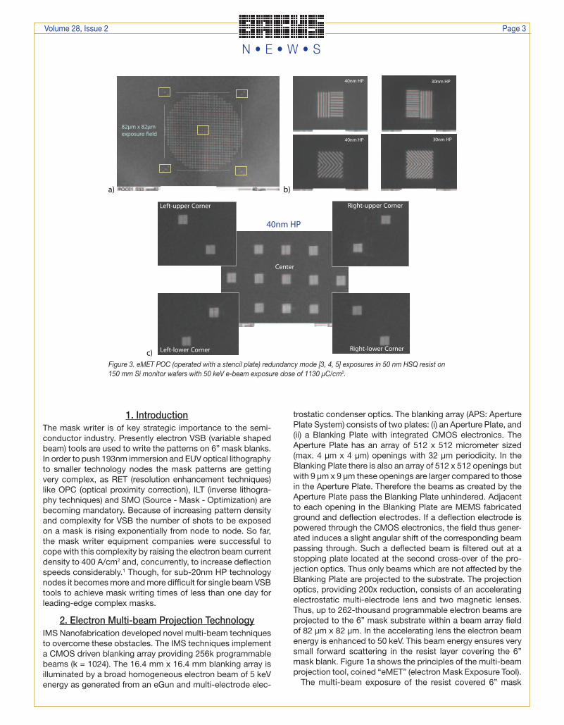
Figure 3. eMET POC (operated with a stencil plate) redundancy mode [3, 4, 5] exposures in 50 nm HSQ resist on 150 mm Si monitor wafers with 50 keV e-beam exposure dose of 1130 µC/cm2.
Volume 28, Issue 2 Page 3
N • E • W • S
blank is done at constant stage speed in stripes of 82 µm width. The stage movement is laser-interferometer controlled and electronic beam tracking is accomplished with the help of multipoles in X/Y, and with an axial solenoid for Q. The multi-beam exposure is done in a sophisticated redundancy mode whose level can be chosen (4-times, 8-times or 16-times redundancy). There is the possibility of in-situ changing the beam size, e.g. 10 nm instead of 20 nm (Figure 2).
The column is designed for a current per beam of max. 4 pA. Thus, for 10 nm beam size the current density is as low as 4 A/cm2. Such low current density provides decisive advantages: the current density at the APS is 40-thousand times lower thus minimizing risk of contamination. Further, there is effective differential pumping in the column. The low current density at the substrate largely reduces local resist heating and hence causes only very low beaminduced resist outgassing.
If all beams are “on” they add up to a total current of c. 1 µA. Careful analysis shows that the performance of the multi-beam projection mask writer is not affected by Coulomb interactions (residual errors are very small).4 Instead, the throughput is governed by the speed of the APS CMOS electronics and the speed of the Data Path to the APS.
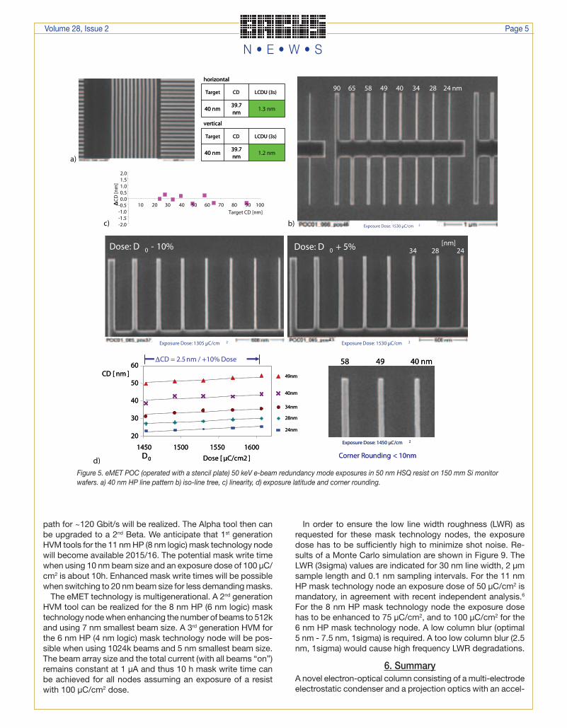
3. eMET POC Column Test ResultsA proof-of-concept electron mask exposure tool (eMET POC) was realized in the first half of 2011 (Figure 1b). The tool is equipped with a Philips laser-interferometer controlled X/Y stage with 1 nm 1sigma performance. For “Beam On” and Q3 2011 exposures the eMET POC was operated with a stencil plate providing 784 beams of 20 nm beam size within a 82 µm x 82 µm beam array field (Figure 3a). Pattern exposure was accomplished with multipole X/Y steering of all beams in paral-lel realizing complex patterns with 2.5 µm periodicity. Figure 3c shows 40 nm HP line pattern resolution achieved over the 82 µm x 82 µm beam array field. Higher magnification SEM images of 40 nm HP and 30 nm HP line patterns are shown in Figure 3b. The exposures were done in 50 nm HSQ negative resist on 150 mm Si monitor wafers.
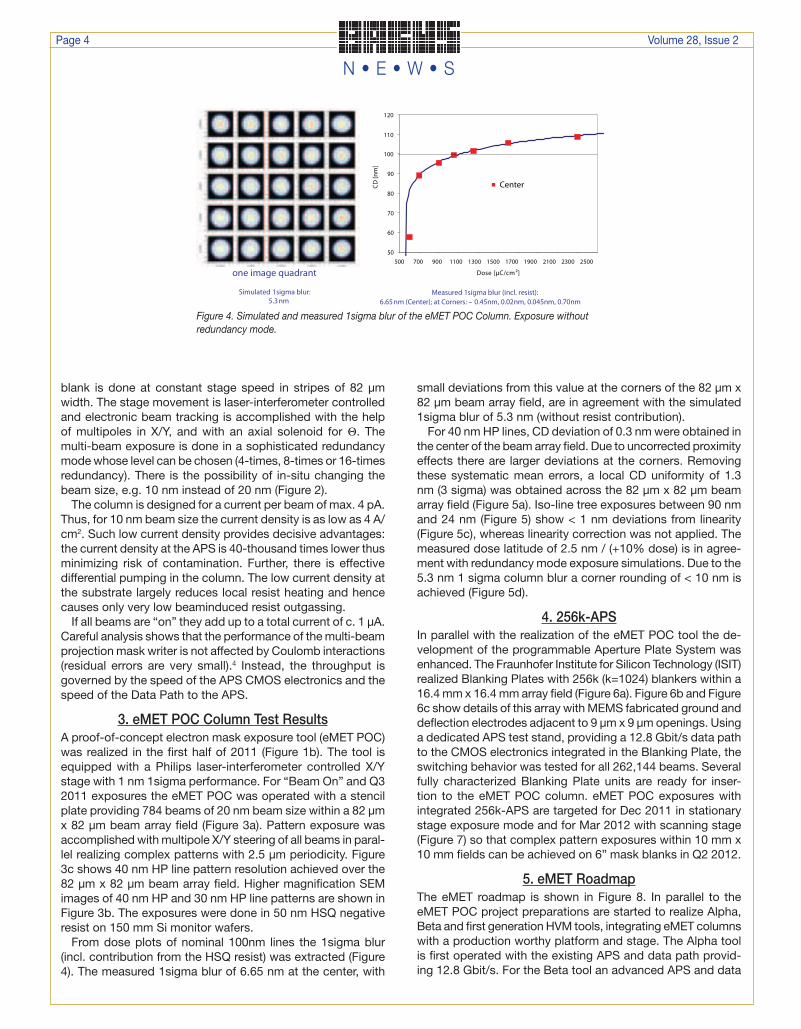
From dose plots of nominal 100nm lines the 1sigma blur (incl. contribution from the HSQ resist) was extracted (Figure 4). The measured 1sigma blur of 6.65 nm at the center, with
small deviations from this value at the corners of the 82 µm x 82 µm beam array field, are in agreement with the simulated 1sigma blur of 5.3 nm (without resist contribution).
For 40 nm HP lines, CD deviation of 0.3 nm were obtained in the center of the beam array field. Due to uncorrected proximity effects there are larger deviations at the corners. Removing these systematic mean errors, a local CD uniformity of 1.3 nm (3 sigma) was obtained across the 82 µm x 82 µm beam array field (Figure 5a). Iso-line tree exposures between 90 nm and 24 nm (Figure 5) show < 1 nm deviations from linearity (Figure 5c), whereas linearity correction was not applied. The measured dose latitude of 2.5 nm / (+10% dose) is in agree-ment with redundancy mode exposure simulations. Due to the 5.3 nm 1 sigma column blur a corner rounding of < 10 nm is achieved (Figure 5d).
4. 256k-APSIn parallel with the realization of the eMET POC tool the de-velopment of the programmable Aperture Plate System was enhanced. The Fraunhofer Institute for Silicon Technology (ISIT) realized Blanking Plates with 256k (k=1024) blankers within a 16.4 mm x 16.4 mm array field (Figure 6a). Figure 6b and Figure 6c show details of this array with MEMS fabricated ground and deflection electrodes adjacent to 9 µm x 9 µm openings. Using a dedicated APS test stand, providing a 12.8 Gbit/s data path to the CMOS electronics integrated in the Blanking Plate, the switching behavior was tested for all 262,144 beams. Several fully characterized Blanking Plate units are ready for inser-tion to the eMET POC column. eMET POC exposures with integrated 256k-APS are targeted for Dec 2011 in stationary stage exposure mode and for Mar 2012 with scanning stage (Figure 7) so that complex pattern exposures within 10 mm x 10 mm fields can be achieved on 6” mask blanks in Q2 2012.
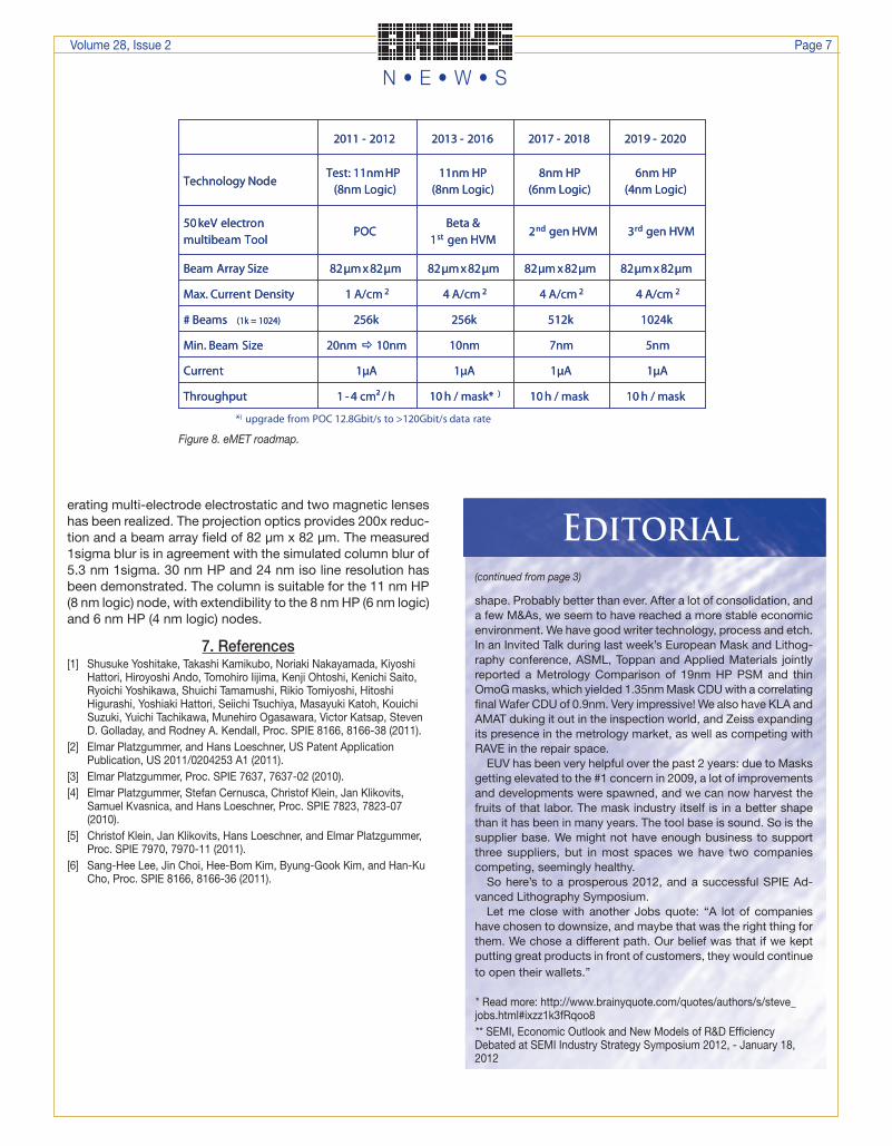
5. eMET RoadmapThe eMET roadmap is shown in Figure 8. In parallel to the eMET POC project preparations are started to realize Alpha, Beta and first generation HVM tools, integrating eMET columns with a production worthy platform and stage. The Alpha tool is first operated with the existing APS and data path provid-ing 12.8 Gbit/s. For the Beta tool an advanced APS and data
Figure 4. Simulated and measured 1sigma blur of the eMET POC Column. Exposure without redundancy mode.
Page 4 Volume 28, Issue 2
N • E • W • S
path for ~120 Gbit/s will be realized. The Alpha tool then can be upgraded to a 2nd Beta. We anticipate that 1st generation HVM tools for the 11 nm HP (8 nm logic) mask technology node will become available 2015/16. The potential mask write time when using 10 nm beam size and an exposure dose of 100 µC/cm2 is about 10h. Enhanced mask write times will be possible when switching to 20 nm beam size for less demanding masks.
The eMET technology is multigenerational. A 2nd generation HVM tool can be realized for the 8 nm HP (6 nm logic) mask technology node when enhancing the number of beams to 512k and using 7 nm smallest beam size. A 3rd generation HVM for the 6 nm HP (4 nm logic) mask technology node will be pos-sible when using 1024k beams and 5 nm smallest beam size. The beam array size and the total current (with all beams “on”) remains constant at 1 µA and thus 10 h mask write time can be achieved for all nodes assuming an exposure of a resist with 100 µC/cm2 dose.
In order to ensure the low line width roughness (LWR) as requested for these mask technology nodes, the exposure dose has to be sufficiently high to minimize shot noise. Re-sults of a Monte Carlo simulation are shown in Figure 9. The LWR (3sigma) values are indicated for 30 nm line width, 2 µm sample length and 0.1 nm sampling intervals. For the 11 nm HP mask technology node an exposure dose of 50 µC/cm2 is mandatory, in agreement with recent independent analysis.6 For the 8 nm HP mask technology node the exposure dose has to be enhanced to 75 µC/cm2, and to 100 µC/cm2 for the 6 nm HP mask technology node. A low column blur (optimal 5 nm - 7.5 nm, 1sigma) is required. A too low column blur (2.5 nm, 1sigma) would cause high frequency LWR degradations.
6. SummaryA novel electron-optical column consisting of a multi-electrode electrostatic condenser and a projection optics with an accel-
Figure 5. eMET POC (operated with a stencil plate) 50 keV e-beam redundancy mode exposures in 50 nm HSQ resist on 150 mm Si monitor wafers. a) 40 nm HP line pattern b) iso-line tree, c) linearity, d) exposure latitude and corner rounding.
Volume 28, Issue 2 Page 5
N • E • W • S
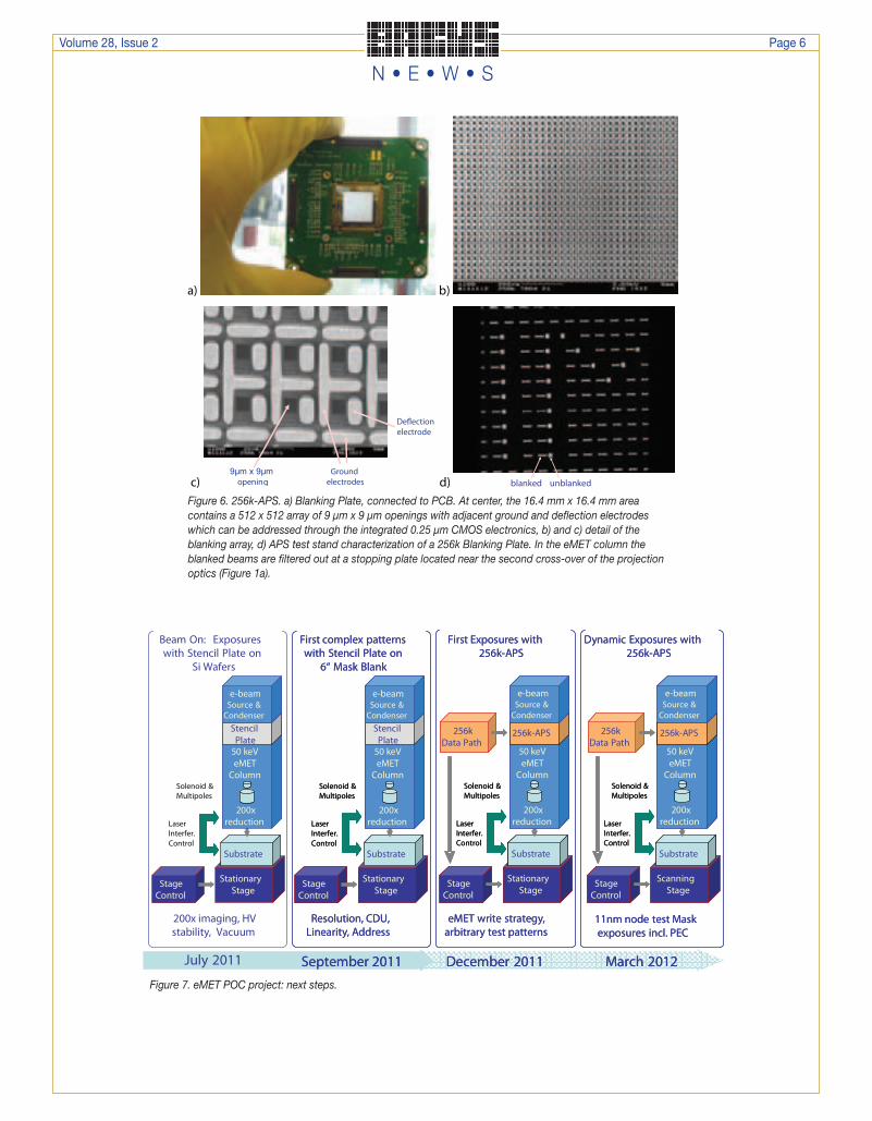
Figure 6. 256k-APS. a) Blanking Plate, connected to PCB. At center, the 16.4 mm x 16.4 mm area contains a 512 x 512 array of 9 µm x 9 µm openings with adjacent ground and deflection electrodes which can be addressed through the integrated 0.25 µm CMOS electronics, b) and c) detail of the blanking array, d) APS test stand characterization of a 256k Blanking Plate. In the eMET column the blanked beams are filtered out at a stopping plate located near the second cross-over of the projection optics (Figure 1a).
Figure 7. eMET POC project: next steps.
Volume 28, Issue 2 Page 6
N • E • W • S
erating multi-electrode electrostatic and two magnetic lenses has been realized. The projection optics provides 200x reduc-tion and a beam array field of 82 µm x 82 µm. The measured 1sigma blur is in agreement with the simulated column blur of 5.3 nm 1sigma. 30 nm HP and 24 nm iso line resolution has been demonstrated. The column is suitable for the 11 nm HP (8 nm logic) node, with extendibility to the 8 nm HP (6 nm logic) and 6 nm HP (4 nm logic) nodes.
7. References[1] Shusuke Yoshitake, Takashi Kamikubo, Noriaki Nakayamada, Kiyoshi
Hattori, Hiroyoshi Ando, Tomohiro Iijima, Kenji Ohtoshi, Kenichi Saito, Ryoichi Yoshikawa, Shuichi Tamamushi, Rikio Tomiyoshi, Hitoshi Higurashi, Yoshiaki Hattori, Seiichi Tsuchiya, Masayuki Katoh, Kouichi Suzuki, Yuichi Tachikawa, Munehiro Ogasawara, Victor Katsap, Steven D. Golladay, and Rodney A. Kendall, Proc. SPIE 8166, 8166-38 (2011).
[2] Elmar Platzgummer, and Hans Loeschner, US Patent Application Publication, US 2011/0204253 A1 (2011).
[3] Elmar Platzgummer, Proc. SPIE 7637, 7637-02 (2010).[4] Elmar Platzgummer, Stefan Cernusca, Christof Klein, Jan Klikovits,
Samuel Kvasnica, and Hans Loeschner, Proc. SPIE 7823, 7823-07 (2010).
[5] Christof Klein, Jan Klikovits, Hans Loeschner, and Elmar Platzgummer, Proc. SPIE 7970, 7970-11 (2011).
[6] Sang-Hee Lee, Jin Choi, Hee-Bom Kim, Byung-Gook Kim, and Han-Ku Cho, Proc. SPIE 8166, 8166-36 (2011).
10 h / mask10 h / mask10 h / mask* )1 - 4 cm2 / hThroughput
1µA1µA1µA1µACurrent
2019 - 20202017 - 20182013 - 20162011 - 2012
4 A/cm 24 A/cm 24 A/cm 21 A/cm 2Max. Current Density
5nm7nm10nm20nm 10nmMin. Beam Size
1024k512k256k256k# Beams (1k = 1024)
82µm x 82µm82µm x 82µm82µm x 82µm82µm x 82µmBeam Array Size
3rd gen HVM2nd gen HVMBeta &
1st gen HVMPOC
50 keV electronmultibeam Tool
6nm HP(4nm Logic)
8nm HP(6nm Logic)
11nm HP(8nm Logic)
Test: 11nmHP(8nm Logic)
Technology Node
*) upgrade from POC 12.8Gbit/s to >120Gbit/s data rate Figure 8. eMET roadmap.
shape. Probably better than ever. After a lot of consolidation, and a few M&As, we seem to have reached a more stable economic environment. We have good writer technology, process and etch. In an Invited Talk during last week’s European Mask and Lithog-raphy conference, ASML, Toppan and Applied Materials jointly reported a Metrology Comparison of 19nm HP PSM and thin OmoG masks, which yielded 1.35nm Mask CDU with a correlating final Wafer CDU of 0.9nm. Very impressive! We also have KLA and AMAT duking it out in the inspection world, and Zeiss expanding its presence in the metrology market, as well as competing with RAVE in the repair space.
EUV has been very helpful over the past 2 years: due to Masks getting elevated to the #1 concern in 2009, a lot of improvements and developments were spawned, and we can now harvest the fruits of that labor. The mask industry itself is in a better shape than it has been in many years. The tool base is sound. So is the supplier base. We might not have enough business to support three suppliers, but in most spaces we have two companies competing, seemingly healthy.
So here’s to a prosperous 2012, and a successful SPIE Ad-vanced Lithography Symposium.
Let me close with another Jobs quote: “A lot of companies have chosen to downsize, and maybe that was the right thing for them. We chose a different path. Our belief was that if we kept putting great products in front of customers, they would continue to open their wallets.”
* Read more: http://www.brainyquote.com/quotes/authors/s/steve_jobs.html#ixzz1k3fRqoo8** SEMI, Economic Outlook and New Models of R&D Efficiency Debated at SEMI Industry Strategy Symposium 2012, - January 18, 2012
Editorial(continued from page 3)
Volume 28, Issue 2 Page 7
N • E • W • S
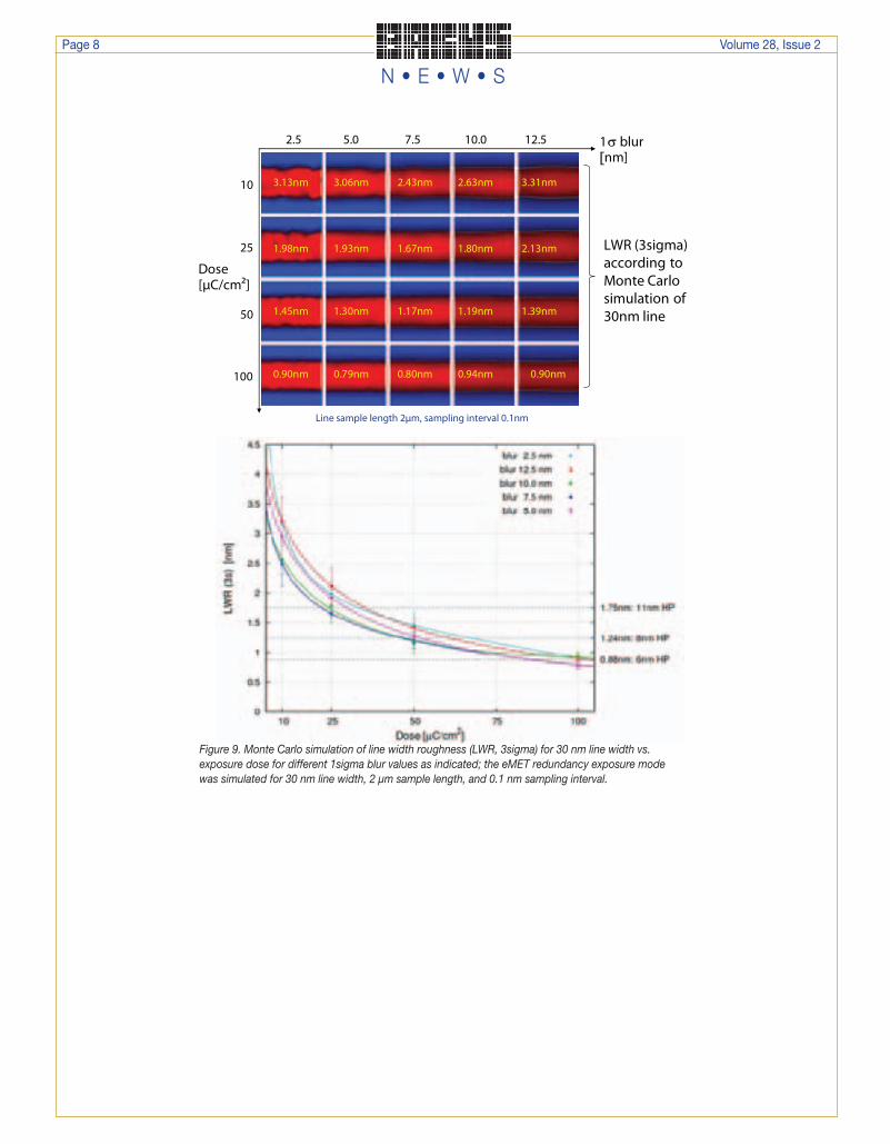
Figure 9. Monte Carlo simulation of line width roughness (LWR, 3sigma) for 30 nm line width vs. exposure dose for different 1sigma blur values as indicated; the eMET redundancy exposure mode was simulated for 30 nm line width, 2 µm sample length, and 0.1 nm sampling interval.
Page 8 Volume 28, Issue 2
N • E • W • S
N • E • W • S
Sponsorship OpportunitiesSign up now for the best sponsorship opportunities for Photomask 2012 and Advanced Lithography 2012.
Contact:Lara Miles
Tel: +1 360 676 3290 [email protected]
Advertise in the BACUS News!
The BACUS Newsletter is the premier publication serving the photomask industry. For information on how to advertise, contact:
Lara MilesTel: +1 360 676 3290
BACUS Corporate Members
FUJIFILM Electronic Materials U.S.A., Inc.Gudeng Precision Industrial Co., Ltd.HamaTech APE GmbH & Co. KGHitachi High Technologies America, Inc.Ibss Group, Inc.JEOL USA Inc.KLA-Tencor Corp.Max Levy Autograph, Inc.Mentor Graphics Corp.Mentor Graphics Corp.Molecular Imprints, Inc.Plasma-Therm LLCRaytheon ELCAN Optical TechnologiesXYALIS
■ 3D integration key to 22nm semiconductor devices
Paul Lindner, EV Group (EVG) 3D IC integration offers smaller footprint, lower power, higher bandwidth, low complexity and cost due to the ability to partition large, complex dies into smaller functional blocks, enabling a modular design with standardized components. All of these benefits can be combined with aggressively scaled devices down to 22nm. Intel’s development of a 22nm trigate transistor is well under way, with volume manufacturing the next hurdle to be cleared. Micron, Samsung and Elpida are building momentum for 3D technology in high-speed, high-bandwidth memory, IDMs, foundries and OSATs are all investing into 3D capacity. Fabless companies like Qualcomm are very actively engaged in building supply chains for 3D. Key challenges in reaching time-to-market goals include (not-untypically), process integration, process stability, and yield.
■ Intel makes way for Ivy Bridge; discontinues 25 CPUs
Sylvie BarakIntel has notified hardware partners it will be phasing out production of 25 desktop CPU models to make way for its new 22nm Ivy Bridge processors due out in April. The chipmaker will be slowing production of the Core i5-661/660, Core i3-530, Pentium E5700 and Celeron E3500, before halting them altogether in the second quarter. Intel’s new CPU platform is Maho Bay, which includes the Ivy Bridge CPU and Panther Point chipset. While the official launch is expected in early April, mainboard makers like Taiwanese Gigabyte have said early motherboard samples will be on show at both CES and CeBit. For those waiting to upgrade to Ivy Bridge, the difference boils down to better integrated graphics and lower power owing to the 22-nm process. Ivy Bridge chips will have DX11 graphics included and overall performance is expected to be significantly higher.
■ 20nm mask technology relies on SMO and DTP
Franklin Kalk, Toppan PhotomasksWith the first 20nm test chips coming out, the mask production toolkit and materials have been selected and installed at the leading mask houses. Mask patterns are already complex due to the pervasive use of OPC and SMO. This pattern complexity drives electron beam shot count, which in turn determines mask write time. The mask blank and resist materials have been changed to include thinner resists, thinner hard mask and thinner absorber layer with adjusted composition. Double-patterning offers relaxed pitch and pattern complexity compared to single patterning, but it requires strict pattern placement and CD accuracy. This will challenge mask writing tool and metrology accuracy. Pattern placement accuracy can be improved with charge effect compensation and e-beam drift correction. Pattern loading compensation can improve CD accuracy regardless of the neighborhood around a feature. At the moment, 28nm technology is entering volume production at the leading foundries. In two or three years, 20nm will be in the same position, and its successful introduction will be enabled in part by the mask technology work in 2012.
■ EVG integrates UV lithography from Eulitha on mask aligner
EV Group, wafer fab equipment provider, signed a joint-development and licensing agreement with lithography company Eulitha AG, integrating Eulitha’s PHABLE mask-based ultraviolet photolithography technology with EVG’s automated mask aligner product platform. The aim is low cost of ownership nanopatterning of high-brightness light emitting diodes. EVG plans to offer a PHABLE-enabled EVG620 system as an extension to its well-established mask alignment system platform. Demo capabilities are already in place, and the first products are expected to ship later in 2012. Eulitha AG, a spin-off company of the Paul Scherrer Institute, Switzerland, specializes in the development of innovative lithographic technologies for applications in optoelectronics, photonics, biotechnology, and data storage. EV Group supplies wafer bonding, lithography/nanoimprint lithography (NIL) and metrology equipment, as well as photoresist coaters, cleaners and inspection systems for semiconductor, MEMS and nanotechnology applications.
■ GLOBALFUNDRIES’ N.Y. fab kick starts production with IBM deal
Dylan McGrath GLOBALFOUNDRIES commenced product at the 300-mm fab in Malta, N.Y., by building 32-nm chips for IBM Corp.. The chips are being built based on IBM’s silicon-on-insulator (SOI) technology and will be in volume production in the second half of 2012. GLOBALFOUNDRIES’ new Fab 8 campus is located in the Luther Forest Technology Campus about 100 miles north of the IBM East Fishkill, N.Y. It is the largest leading-edge semiconductor foundry facility in the U.S.. When fully ramped, the total clean-room space will be approximately 300,000 square feet capable of a total output of approximately 60,000 wafers per month. The fab will focus on leading-edge manufacturing at 32- and 28-nm and below. The chips GLOBALFOUNDRIES is manufacturing for IBM feature embedded dynamic random access memory (eDRAM) technology, to improve on-processor memory performance in about one-third the space with one-fifth the standby power of conventional SRAM.
Volume 28, Issue 2 Page 9
N • E • W • S
Industry Briefs

SPIE is the international society for optics and photonics.
International HeadquartersP.O. Box 10, Bellingham, WA 98227-0010 USA Tel: +1 360 676 3290 Fax: +1 360 647 [email protected] • SPIE.org
Shipping Address1000 20th St., Bellingham, WA 98225-6705 USA
2 Alexandra Gate, Ffordd Pengam, Cardiff, CF24 2SA, UK Tel: +44 29 2089 4747 Fax: +44 29 2089 [email protected] • www.spieeurope.org
2012
Advanced Lithography
12-16 February 2012San Jose Convention Center and San Jose MarriottSan Jose, California, USAspie.org/al
SPIE Photomask Technology
10-13 September 2012Monterey Marriott and Monterey Conference CenterMonterey, California, USAspie.org/pm
Corporate Membership Benefits include:■ Three Voting Members in the SPIE General Membership
■ Subscription to BACUS News (monthly)
■ One online SPIE Journal Subscription
■ Listed as a Corporate Member in the BACUS Monthly Newsletter spie.org/bacushome
C
a
l
e
n
d
a
r
About the BACUS GroupFounded in 1980 by a group of chrome blank users wanting a single voice to interact with suppliers, BACUS has grown to become the largest and most widely known forum for the exchange of technical information of interest to photomask and reticle makers. BACUS joined SPIE in January of 1991 to expand the exchange of information with mask makers around the world.
The group sponsors an informative monthly meeting and newsletter, BACUS News. The BACUS annual Photomask Technology Symposium covers photomask technology, photomask processes, lithography, materials and resists, phase shift masks, inspection and repair, metrology, and quality and manufacturing management.
Individual Membership Benefits include:■ Subscription to BACUS News (monthly)
■ Complimentary Subscription Semiconductor International magazine
■ Eligibility to hold office on BACUS Steering Committee
spie.org/bacushome
You are invited to submit events of interest for this calendar. Please send to
[email protected]; alternatively, email or fax to SPIE.h
h
Join the premier professional organization for mask makers and mask users!
Volume 28, Issue 2 Page 10
N • E • W • S