Embed Size (px)
Citation preview
Thin Film Encapsulation Methods for Large Area MEMS Packaging
By
Armon Mahajerin
A dissertation submitted in partial satisfaction of the
requirements in the degree of
Doctor of Philosophy
in
Engineering – Mechanical Engineering
and the Designated Emphasis
in
Nanoscale Science & Engineering
in the
Graduate Division
of the
University of California, Berkeley
Committee in charge:
Professor Liwei Lin, Chair
Professor Dorian Liepmann
Professor Tsu-Jae King Liu
Spring 2012
Thin Film Encapsulation Methods for Large Area MEMS Packaging
Copyright 2012
by
Armon Mahajerin
1
Abstract
Thin Film Encapsulation Methods for Large Area MEMS Packaging
by
Armon Mahajerin
Doctor of Philosophy in Engineering – Mechanical Engineering
and the Designated Emphasis in Nanoscale Science and Engineering
University of California, Berkeley
Professor Liwei Lin, Chair
The past thirty years have seen rapid growth in products and technologies based on
microelectromechanical systems (MEMS). However, one of the limiting factors in
commercializing MEMS devices is packaging, which can be the most costly step in the
manufacturing process. A MEMS package must protect the movable parts of the device while
allowing it to interact with its surroundings. In addition, the miniaturization of sensors and
actuators has made it possible to integrate MEMS fabrication with that of integrated circuit (IC)
processing. Due to the varying requirements for different applications, a universal standard for
packaging MEMS has been elusive. However, a growing trend has been the shift away from
bonding a separate sealing substrate to the device substrate and toward thin film encapsulation.
The latter method has the potential to reduce costs and materials usage while increasing device
throughput and yield.
Two thin film encapsulation methods for creating large area packaged cavities on top of
silicon substrates have been developed based on porous membrane structures. The first approach
uses thin polysilicon as a permeable membrane. The polysilicon is deposited on top of a doped
oxide using low pressure chemical vapor deposition (LPCVD) to a thickness less than 300 nm.
High temperature annealing drives the dopant atoms from the oxide into the polysilicon film,
creating gaps within the film through which hydrofluoric acid (HF) vapor penetrates and etches
the buried oxide. In addition, a process of rapidly depositing oxides greater than 10 μm thick
without cracking due to residual stress has also been demonstrated. This is accomplished by
using plasma enhanced chemical vapor deposition (PECVD) steps of 2.5 μm thickness with
interceding rapid thermal annealing (RTA). The permeable polysilicon membrane technology
provides the foundation for wafer-level encapsulation of MEMS devices inside the cavities by
depositing a thick structural layer either under vacuum or at arbitrary pressure environments.
The thin permeable polysilicon technique then evolves into a broader encapsulation
method in which a semi-permeable film is constructed from carbon nanotubes (CNTs) and
polysilicon. The dense forest of CNTs may be grown to a height from 10 μm to hundreds of μm
2
as the structural foundation for the encapsulation layer. Conformally coating the CNTs with
polysilicon by LPCVD generates natural pores within the thick membrane. HF vapor penetrates
the semi-permeable film to selectively etch the bottom oxide layer, after which another
polysilicon deposition seals the film, rendering it impermeable. The etching behavior has been
characterized as a function of the CNT height and exposure time to HF vapor. The
CNT/polysilicon thickness for a given vacuum-sealed cavity area has also been designed using
finite element analysis (FEA). Furthermore, large sealing areas of more than 1x1 mm2 have been
successfully demonstrated. As such, this wafer-level encapsulation technology could find
potential packaging applications of MEMS devices, including large area gyroscope structures.

i
“I'll be honest.
We’re throwing science at the walls here to see what sticks.
No idea what it’ll do.”
- Cave Johnson
For Tatar

ii
Contents
List of Figures ................................................................................................................................ v
List of Tables ................................................................................................................................. x
1. Introduction ............................................................................................................................ 1
1.1 Microelectromechanical Systems ..................................................................................... 1
1.2 MEMS Fabrication ........................................................................................................... 2
1.3 Packaging ......................................................................................................................... 5
1.4 Dissertation Overview ...................................................................................................... 6
2. MEMS Packaging Overview ................................................................................................. 8
2.1 Background ...................................................................................................................... 8
2.1.1 Packaging Considerations ......................................................................................... 8
2.1.2 Challenges of Packaging MEMS .............................................................................. 9
2.2 Wafer Level Packaging .................................................................................................. 14
2.2.1 Overview of Wafer Level Processes ....................................................................... 14
2.2.2 Interfacial Bonding ................................................................................................. 14
2.2.3 Thin Films ............................................................................................................... 20
2.2.4 Electrical Feedthrough ............................................................................................ 26
2.3 Summary ........................................................................................................................ 27
3. Thin Film Encapsulation Using Permeable Polysilicon ................................................... 29
3.1 Project Background ........................................................................................................ 29
3.1.1 Motivation ............................................................................................................... 29
3.1.2 Device Overview .................................................................................................... 29
3.1.3 Initial Fabrication Process....................................................................................... 32
3.2 Modeling and Design ..................................................................................................... 34
3.2.1 Theory of Membrane Behavior ............................................................................... 34
3.2.2 Polysilicon Membrane ............................................................................................ 35

iii
3.2.3 Thick TEOS as Membrane ...................................................................................... 41
3.2.4 Mask Design ........................................................................................................... 43
3.3 Assessing Permeability of Polysilicon ........................................................................... 45
3.3.1 Preliminary Studies ................................................................................................. 45
3.3.2 Modified Fabrication Process Using TEOS Cap .................................................... 49
3.4 Characterizing Etching Behavior ................................................................................... 50
3.4.1 HF Vapor Penetration ............................................................................................. 50
3.4.2 Using a Silicon Nitride Hard Mask ......................................................................... 52
3.5 Deposition of Thick TEOS Films .................................................................................. 55
3.5.1 Issue with TEOS Cracking...................................................................................... 55
3.5.2 Rapid Thermal Annealing ....................................................................................... 56
3.5.3 Results of TEOS + RTA ......................................................................................... 58
3.6 Summary ........................................................................................................................ 60
4. Large Area Encapsulation Using Carbon Nanotube/Polysilicon Composites ............... 61
4.1 Overview ........................................................................................................................ 61
4.1.1 Motivation ............................................................................................................... 61
4.1.2 Carbon Nanotube Background ................................................................................ 61
4.1.3 Carbon Nanotube Growth ....................................................................................... 63
4.1.4 Proposed CNT/Polysilicon Composite ................................................................... 65
4.2 Preliminary Results ........................................................................................................ 66
4.2.1 Fabrication Process ................................................................................................. 66
4.2.2 CNT Growth and Polysilicon Deposition ............................................................... 68
4.2.3 Permeability of Composite Film ............................................................................. 71
4.3 Modeling Deflection of the Composite Film ................................................................. 75
4.3.1 Reasoning for Measuring Deflection ...................................................................... 75
4.3.2 Theory for Plate Deflection .................................................................................... 77
4.3.3 Membrane Deflection Calculations and FEA ......................................................... 79
4.3.4 Design Methodology ............................................................................................... 83
4.4 Process Characterization ................................................................................................ 84
4.4.1 Over-Etch Behavior ................................................................................................ 84
iv
4.4.2 Encapsulation and Deflection Under Vacuum ........................................................ 87
4.5 Summary ........................................................................................................................ 89
5. Conclusions and Future Work ............................................................................................ 91
5.1 Conclusions .................................................................................................................... 91
5.2 Future Work ................................................................................................................... 93
5.2.1 Redesign of Composite Membrane ......................................................................... 93
5.2.2 Characterizing Sealing Conditions ......................................................................... 94
5.2.3 Process Flow for Integrated MEMS Device ........................................................... 95
References .................................................................................................................................... 98
v
List of Figures
Figure 1.1. Bulk micromachining using anisotropic etching. ......................................................... 3
Figure 1.2. Surface micromachining with use of a sacrificial layer. .............................................. 4
Figure 1.3. Sample MEMS package with multiple interfaces. [17]................................................ 5
Figure 1.4. Schematic diagrams for thin film encapsulation using: (a) permeable polysilicon, and
(b) composites of carbon nanotubes and polysilicon. ..................................................................... 6
Figure 2.1. Comparison of die level and wafer level packaging. ................................................... 9
Figure 2.2. Schematics of (a) an IC package and (b) a MEMS pressure sensor package. [21] .... 10
Figure 2.3. Stiction of MEMS structures to silicon substrate after release................................... 11
Figure 2.4. Effect of mismatch of coefficient of thermal expansion (CTE) on film stress. ......... 12
Figure 2.5. Cross section of an interfacial capsule or shell bonded to a substrate. [17] ............... 15
Figure 2.6. Anodic bonding schematic showing (a) procedure with top tool functioning as a
cathode and the chuck as an anode, and (b) ion drift in the Pyrex glass as a result of the electric
field, forming a depletion zone at the interface to which O- ions drift. ........................................ 16
Figure 2.7. Schematic diagram of Au-Si eutectic bonding for packaging a silicon cap wafer to a
MEMS device wafer, (a) before bonding and (b) after bonding. [62] .......................................... 17
Figure 2.8. Schematic of localized bonding using on-chip resistors. [17] .................................... 18
Figure 2.9. SEM photograph of an encapsulated microresonator under a glass cap. [84] ............ 19
Figure 2.10. Schematic diagram of thermo-compressive Au-Au diffusion bonding. [85] ........... 20
Figure 2.11. Comparison of MEMS device packages sealed by using (a) a thin film membrane or
(b) a bonded capsule. [17] ............................................................................................................. 21
Figure 2.12. Fabrication flow schematic for a thin film shell with etch channels: (a) device and
etch channel formation; (b) second sacrificial layer deposition and encapsulation layer
patterning; (c) simultaneous removal of both sacrificial layers; (d) sealing of encapsulation shell.
[102] .............................................................................................................................................. 22
Figure 2.13. Image of thin film encapsulated accelerometers: (a) released structure; (b) detailed
cross-sectional view. [107] ........................................................................................................... 23
Figure 2.14. Monolithically encapsulated Pirani gauge using porous alumina: (a) SEM
photograph of the device under a broken shell; (b) cross-sectional view of the cavity. [116] ..... 24
Figure 2.15. Fabrication process for creating electroplated nickel vacuum packages. [117] ....... 25
Figure 2.16. Schematic of fabrication process for epitaxial polysilicon encapsulation. [122] ..... 25

vi
Figure 2.17. Lateral feedthrough process flow for anodic bonding: (a) pattern oxide; (b) deposit
metal; (c) lift-off; (d) SOG coating; (e) Si sputtering; (f) Pyrex cap anodic bonding. ................. 26
Figure 2.18. Vertical electrical feedthrough with filled via holes in a Pyrex wafer. [128] .......... 27
Figure 3.1. Four accelerometer designs, each with different package dimensions and positions of
the bonding pads. .......................................................................................................................... 30
Figure 3.2. Overview of device structural components. ............................................................... 31
Figure 3.3. Generic fabrication process for SOI wafers. .............................................................. 32
Figure 3.4. Preliminary fabrication process for thin film encapsulation using thin polysilicon. (a)
Begin with patterned SOI wafer; (b) deposit thick TEOS sacrificial layer via PECVD; (c)
LPCVD thin polysilicon; (d) pattern photoresist to create etch windows and expose wafer to HF
for removing underlying oxide; (e) seal cavity and strengthen membrane against deflection with
additional polysilicon or silicon carbide. ...................................................................................... 33
Figure 3.5. Rectangular plate fixed along all edges under uniformly distributed load ................. 34
Figure 3.6. Schematic of pressure load causing thin membranes to deform. ............................... 36
Figure 3.7. FEA mesh area and pillar supports for generic thin polysilicon film......................... 37
Figure 3.8. Two-dimensional plot of maximum deflection for a 20 μm thick polysilicon
membrane under vacuum load. ..................................................................................................... 38
Figure 3.9. Large area bonding pads on MEMS devices used as support pillars at each corner for
thin membranes; smaller pads also may be treated as pillars to support polysilicon film. ........... 39
Figure 3.10. 2D models in ANSYS for each membrane configuration based on support pad
positions, showing maximum deflection under vacuum load at the center of each film. ............. 40
Figure 3.11. Positioning of large bonding pads and smaller pads connected to comb drives. ..... 41
Figure 3.12. Maximum film deflection vs. TEOS thickness for four different configurations. ... 42
Figure 3.13. 2D deflection profiles of 15 μm thick TEOS membranes in four device designs. ... 43
Figure 3.14. Lateral undercut required for release of movable fingers (not to scale). .................. 44
Figure 3.15. Lateral undercut of bonding pad pillars (not to scale). ............................................. 44
Figure 3.16. Comparison of “conservative” and “original” etch mask layouts. ........................... 45
Figure 3.17. Using oxygen plasma to generate gaps at polysilicon grain boundaries. ................. 46
Figure 3.18. Results of annealing and oxygen plasma treatment of polysilicon films. ................ 47
Figure 3.19. Successful penetration of doped polysilion and oxide etching. ............................... 48
Figure 3.20. Revised fabrication steps for thin film encapsulation with doped permeable
polysilicon. (a) Begin with patterned SOI wafers; (b) deposit thick TEOS sacrificial layer via
PECVD; (c) deposit PSG via LPCVD followed by high temperature densification; (d) LPCVD
vii
and patterning of silicon nitride for hard mask; (e) LPCVD of polysilicon followed by dopant
drive in annealing step; (f) HF vapor etching; (g) additional TEOS reinforcement. .................... 49
Figure 3.21. Simplified fabrication process testing HF vapor penetration. (a) LPCVD deposition
of PSG followed by densification; (b) LPCVD of polysilicon followed by dopant anneal; (c)
spinning and patterning of SU8 photoresist for etch mask; (d) oxide removal by HF vapor
penetration of permeable polysilicon. ........................................................................................... 50
Figure 3.22. SEM photographs of: (a) top view of patterned SU8 photoresist mask; and (b) cross-
sectional view of etch holes in suspended SU8 layer. .................................................................. 51
Figure 3.23. SEM photographs showing: (a) suspended SU8 layer above etched cavity; and (b)
PSG removed in select areas on substrate; and (c) thin polysilicon on top of PSG layer. ........... 52
Figure 3.24. Modified fabrication process testing nitride as a hard mask. (a) LPCVD deposition
of PSG followed by densification; (b) LPCVD of silicon nitride; (c) LPCVD of polysilicon
followed by annealing of dopant; (d) oxide removal by HF vapor penetration of permeable
polysilicon. .................................................................................................................................... 53
Figure 3.25. Cross-sectional profiles of fabricated chips after HF vapor exposure times of: (a) 5
minutes; (b) 10 minutes; and (c) 15 minutes, showing the natural progression of HF penetration
and removal of buried oxide underneath the nitride mask. ........................................................... 54
Figure 3.26. Polysilicon etch windows on top of nitride hard mask: (a) after 5 min HF vapor; (b)
roughness of polysilicon window can be seen; (c) close-up of poly roughness from doping; (d)
after 10 min HF vapor; (e) close-up photo of polysilicon windows. ............................................ 55
Figure 3.27. TEOS cracking on fabricated chips at (a) 2x and (b) 5x magnification ................... 56
Figure 3.28. Thick TEOS deposition with rapid thermal annealing: (a) deposit 1st TEOS layer via
PECVD; (b) clean wafer and perform RTA; (c) measure stress in deposited film with laser
interferometer; (d) repeat until desired TEOS thickness is reached ............................................. 57
Figure 3.29. Stress in deposited TEOS films vs. overall thickness. ............................................. 59
Figure 3.30. Film stress of 10 μm TEOS after multiple rapid thermal anneals ............................ 59
Figure 4.1. Three different SWNT structures: (a) armchair; (b) zigzag; (c) chiral. [170] ............ 62
Figure 4.2. Experimental setup for CNT growth on sample chips. .............................................. 64
Figure 4.3. Carbon nanofiber growth resulting from thick Fe catalyst. ........................................ 65
Figure 4.4. Conceptual illustration of a semipermeable encapsulation membrane using a
CNT/polysilicon composite. ......................................................................................................... 66
Figure 4.5. Fabrication process for CNT/polysilicon composite: (a) LPCVD of low-temperature
oxide or PECVD of TEOS oxide; (b) evaporation of metal Al and Fe films; (c) CNT growth via
CVD; (d) first polysilicon LPCVD to conformally coat CNTs; (e) pattern top surface of
polysilicon and plasma etch select area to open membrane pores (f) HF vapor penetration and
oxide removal; (g) second polysilicon LPCVD to seal the film. .................................................. 67
viii
Figure 4.6. CNT growth results for forest heights of: (a) 10 μm, (b) 20 μm, (c) 30 μm, and (d) 40
μm; (e) close up of CNT forest; (f) top view of CNT forest. ........................................................ 69
Figure 4.7. Polysilicon deposition onto CNT forests, showing thickness variation from top to
bottom as well as the natural seal of the top 5 μm of the membrane. ........................................... 70
Figure 4.8. Profile of defined etch window after 4 min plasma etching of polysilicon: (a) cross-
sectional view; (b) top view. ......................................................................................................... 71
Figure 4.9. Polysilicon removal after (a) 3.5 min and (b) 4.5 min plasma etching. ..................... 71
Figure 4.10. HF vapor penetration after 12 minutes on membranes with windows opened by (a)
3.5 min and (b) 4.5 min plasma etches. ........................................................................................ 72
Figure 4.11. Schematic of HF vapor etching of oxide beyond defined cavity width. .................. 73
Figure 4.12. Lateral HF vapor penetration through composite membrane which produces oxide
over-etching. ................................................................................................................................. 73
Figure 4.13. HF vapor undercut for 30 μm sample exposed to 4 min HF vapor: (a) total cavity
width of 825 μm; (b) left side undercut of 153 μm; (c) right side undercut of 161 μm. ............... 75
Figure 4.14. Illustration of plate separation for (a) sealed cavity and (b) unsealed cavity. .......... 76
Figure 4.15. Theoretical capacitance for different cavity sizes as a function of plate separation or
oxide thickness. ............................................................................................................................. 77
Figure 4.16. Predicted deflection under vacuum loading of different square membrane lengths
(different colors) with respect to CNT/polysilicon composite film thickness. ............................. 80
Figure 4.17. Finite element ¼ model of a suspended polysilicon membrane: (a) 285 μm from
edge to center and 20 μm thickness; (b) symmetrical planes surrounding film. .......................... 81
Figure 4.18. Finite element analysis results of a 570 μm x 570 μm x 20 μm polysilicon
membrane: (a) maximum deflection of 1.06 μm, and (b) maximum surface stress of 139 MPa. 81
Figure 4.19. FEA result of deflection under self-weight for a circular membrane 1000 μm in
diameter and 20 μm in thickness................................................................................................... 82
Figure 4.20. Cross-sectional view of etching profile of 7.8 μm thick oxide layer after 8 min HF
vapor for a 20 μm tall encapsulation membrane: (a) suspended membrane with minimal lateral
undercut; (b) close-up of oxide profile after etching by HF vapor. .............................................. 85
Figure 4.21. Comparison of oxide over-etch for 20 μm and 30 μm thick encapsulation
membranes as a function of HF vapor exposure time. .................................................................. 86
Figure 4.22. Oxide over-etch for 25 μm thick membranes as a function of defined cavity
diameter for circular etch windows. .............................................................................................. 87
Figure 4.23. SEM photographs of sealed CNT/polysilicon composite membrane. (a) Step height
at edge of patterned window; (b) membrane suspended over cavity; (c) top view showing sealing
over patterned and unpatterned areas on membrane. .................................................................... 88
ix
Figure 4.24. Surface profile measurements of film deflection after encapsulation over 1000 μm
wide cavities for (a) 25 μm tall membrane, and (b) 45 μm tall membrane. ................................. 89
Figure 5.1. Schematic of reduced over-etch by patterning ribs into composite membrane. ......... 93
Figure 5.2. Hypothetical gap filling between CNT forests by polysilicon. .................................. 94
Figure 5.3. Sample design for a small vacuum test chamber used in conjunction with a laser
interferometer or laser displacement meter. .................................................................................. 95
Figure 5.4. Backside membrane of silicon or silicon nitride used to characterize internal cavity
pressure based on measured deflection. ........................................................................................ 95
Figure 5.5. General process for encapsulating a simple MEMS device and opening electrical
contacts without breaking vacuum................................................................................................ 96
x
List of Tables
Table 2.1. Summary of packaging parameters, challenges, and solutions for MEMS. ................ 13
Table 3.1. Summary of four device designs and relevant dimensions. ......................................... 30
Table 3.2. Maximum deflection for differing polysilicon films spanning large area of 2.65 mm x
1.89 mm. ....................................................................................................................................... 38
Table 3.3. Maximum deflection for each device with 15 μm thick polysilicon membrane ......... 40
Table 3.4. Results of using 0.1 μm polysilicon as permeable layer. ............................................. 46
Table 3.5. Rapid thermal anneal process for TEOS films. ........................................................... 57
Table 3.6. Summary of results for TEOS deposition with RTA. .................................................. 58
Table 4.1. CNT growth process. ................................................................................................... 64
Table 4.2. Summary of oxide over-etch compared to HF vapor exposure time for 30 μm thick
membranes. ................................................................................................................................... 74
Table 4.3. Comparison of maximum deflection and surface stress values obtained by hand or by
FEA for a 570 μm x 570 μm x 20 μm polysilicon membrane. ..................................................... 81
Table 4.4. Upper bounds for square and circular cavity sizes as a function of CNT height for 7.5
μm maximum deflection. .............................................................................................................. 84
Table 4.5. Summary of oxide over-etch compared to HF vapor exposure time for 20 μm thick
membranes. ................................................................................................................................... 85
Table 5.1. Comparison of thin film encapsulation approaches. .................................................... 92
xi
Acknowledgements
The past six years of my life have been engaging, challenging, eye-opening, and
ultimately rewarding. I have many people to thank and hope I do not forget anyone.
First and foremost I owe much to my advisor, Professor Liwei Lin, who welcomed me to
Berkeley and has supported me in many ways throughout my graduate school career. His
encouragement to explore new ideas and not be afraid to take risks has helped me to grow as a
student, researcher, and scholar. I thank him deeply for his patience, guidance, and wisdom.
I also thank Professor Dorian Liepmann and Professor Tsu-Jae King Liu for serving on
my dissertation committee. Their time, feedback, and support have meant a great deal to me.
Professor Liepmann also served as the chair of my qualifying exam committee.
Countless other professors at Berkeley have also stimulated my interests in various
exciting fields and helped guide my learning and research. Most notable are Professor Albert
Pisano, Professor Samuel Mao, Professor Costas Grigoropoulos, Professor Junqiao Wu,
Professor Vivek Subramanian, and Professor Luke Lee. In addition, I would like to acknowledge
Professor John Lloyd and Professor Craig Somerton of Michigan State University for inspiring
me and assisting my path to attend graduate school.
A great deal of the graduate school experience is dependent upon one’s peers. Within the
Lin Lab family, I give thanks to Brian Sosnowchik, Adrienne Higa, Ryan Sochol, Heather
Chiamori, and Kedar Shah for the many hours of random pranks and goofiness amidst the long
hours pondering research challenges on the whiteboard in 1113 Etcheverry. In addition, Yingqi
Jiang and Qin Zhou have provided immeasurable assistance and discussion throughout the past
few years. Their knowledge and kindness have been a blessing. Kevin Limkrailassiri contributed
significantly to the work in Chapter 3 and deserves recognition. Hsieh Shen Hsieh also provided
some assistance in the latter stages of my work. Everyone in the Lin Lab comes to depend on
another person at one point or another, so to the rest of the past and present labmates I give
heartfelt thanks for the memories and support. Outside of the Lin Lab, special thanks go to David
Myers from the Pisano Lab for being another source of aid and guidance.
I would also like to give thanks to the Berkeley Sensor and Actuator Center (BSAC). I’m
really grateful to have had the opportunity to work under this collaborative, interdisciplinary
research group. My advisor and the other co-directors have given researchers a chance to share
our ideas with fellow researchers as well as industry members. The efforts of John Huggins,
Richard Lossing, Kim Ly, Alain Kesseru, and others make everything in BSAC possible, from
the Tuesday lunches to the biannual research reviews. Moreover, thank you to the staff of the
Marvell Nanofabrication Laboratory for making much of our research efforts possible.
My Berkeley experience would not have been complete without the friendship and
support of my peers. From studying for classes in the early years to discussing movies and
politics as a respite from research, my interactions with everyone have positively shaped me and
my time here. In no particular order: Daniel Peters, Chris Zueger, Sara Beaini, Hector Mendoza,
Kenneth Armijo, Kim Ly, Rich Winslow, John Edmiston, Lindsay Miller, Coleman Kronawitter,
xii
Sonia Fereres, and Amanda Dodd. I’m probably forgetting many other people, as it’s been quite
the long journey, but certainly it’s been a pleasure to spend time with everyone. The entity of
Berkeley itself, including the university and the town, has exposed me to great people, cultures,
ideas, and experiences.
Lastly, I thank my family for being so supportive and helping me through these past few
years. Their love and encouragement have been my fuel to make it through the Ph.D. My
brothers, Arash and Ali, have been there for me every step of the way. Arash has provided that
listening ear in crucial moments with a dose of rationality when I needed it, and I owe him for
being available at all times. Ali and my sister-in-law Sonya have sent me all kinds of goodies and
homemade treats to remind me of home and keep my spirits up. The pictures and videos of my
beautiful niece and nephew, Sophia and Ethan, always provided the perfect balance to work and
put a smile on my face every day. Watching them grow up has been very enjoyable.
The older I grow the more I realize how special my parents are. My father has been there
to help me as a loving, caring parent as well as a fellow mechanical engineer. His wisdom and
insight into the Ph.D. process have been immeasurable, and the random jokes were always great
as well. Words cannot express what my mother’s love and support mean to me. The strength and
confidence she has given me have been nothing short of vital. My mother is a truly remarkable
person, and I owe her more than the world has to offer.

1
Chapter 1
Introduction
1.1 Microelectromechanical Systems
Microelectromechanical systems (MEMS) devices have been researched extensively
and developed for a wide variety of applications since the late twentieth century. Essentially,
MEMS are small integrated devices or systems which combine electrical and mechanical
components. They range in size from the sub-micrometer level to the millimeter level and are
fabricated utilizing the technologies developed for the integrated circuit (IC) industry. MEMS
may add mechanical elements such as beams, gears, diaphragms, and springs to existing
devices. Some examples of MEMS applications include accelerometers, inertial sensors,
microengines, miniature robots, micromirrors, inkjet-printer cartridges, micro actuators,
optical scanners, fluidic pumps, transistors, and chemical, pressure, or flow sensors. The
function of these systems is to sense, control, and activate mechanical processes on the micro
scale which integrate and combine to perform macro scale tasks.
MEMS offer a wide variety of advantages related to the scaling down of devices or
systems. For example, by scaling MEMS materials to densities that approach the defect
density of the material, devices may be produced with a very low total number of defects. As
a result some MEMS devices, such as cantilevers whose design is relatively simple, may have
better reliability than their macroscopic versions [1]. At the same time assumptions of
homogeneity for bulk materials may become unreliable when modeling devices on similar
scales as that of individual grains or other microscopic fluctuations in material properties.
Nevertheless, the flexibility of microfabrication permits the properties of thin film materials to
be controlled with high precision [2], [3].
Other scaling advantages of MEMS are evident in fluidic systems, where flow through
microchannels is almost entirely dominated by laminar flow conditions rather than turbulent
and chaotic flows prevalent in most macroscopic systems. Furthermore, in chemical or
biological systems, it’s quite advantageous to reduce the required sample size for a smaller
device while keeping the detectable concentration fixed. It’s also noted that many systems
interfacing with biology are multidisciplinary in nature, requiring fluidic, electronic, and/or
mechanical components. In addition, rapid removal of heat from a microscale object may be
realized since heat can typically conduct in all directions. At the same time it is possible to
fabricate structures which only allow heat transfer along certain directions for good thermal
isolation.

2
The overall importance of MEMS lies in their ability to interface the digital electronic
world with the analog physical world [4]. Due to a wide variety of nonelectrical signals that
exist in the physical world, different transduction mechanisms are required to transducer
physical signals into electrical signals (via sensors). These signals are then processed by IC-
enabled electronic systems and from electric signals into physical signals (via actuators) [5].
Transduction mechanisms may be linked in series, such as from thermal to mechanical to
optical to electrical. In other cases the sensing and actuating mechanisms may be combined
with electronics to form complete microsystems. Overall, the most successful MEMS
products utilize advantageous scaling properties, batch fabrication, and circuit integration.
1.2 MEMS Fabrication
In the early 1980s the term micromachining became a popular designation of
fabricating micromechanical parts, such as pressure-sensor diaphragms or accelerometer
suspension beams, for Si microsensors [6]. These micromechanical parts were fabricated by
selectively etching areas of the Si substrate to form desired geometries. This etching was
accomplished using both isotropic and anisotropic techniques, where the former etches
material at the same rate in different directions through a given material and the latter does
not. These etching processes formed the basis for bulk micromachining (BMM) processing
[7]. BMM has remained a useful technique for fabricating micromechanical structures, but the
need for flexibility in device design and improvements in performance has driven the
development of new concepts and methods of micromachining.
In 1965 researchers developed a technique of creating microstructures using a
sacrificial layer technique [8]. In this method a layer of material is deposited between
structural layers for mechanical separation and isolation. When this layer is removed during a
release etch, the structural layers of the device are given freedom of movement relative to the
substrate. The application of sacrificial layer techniques to micromachining inspired the
growth of surface micromachining (SMM), in which the Si substrate serves as a mechanical
support upon which various micromechanical elements are deposited, patterned, and etched in
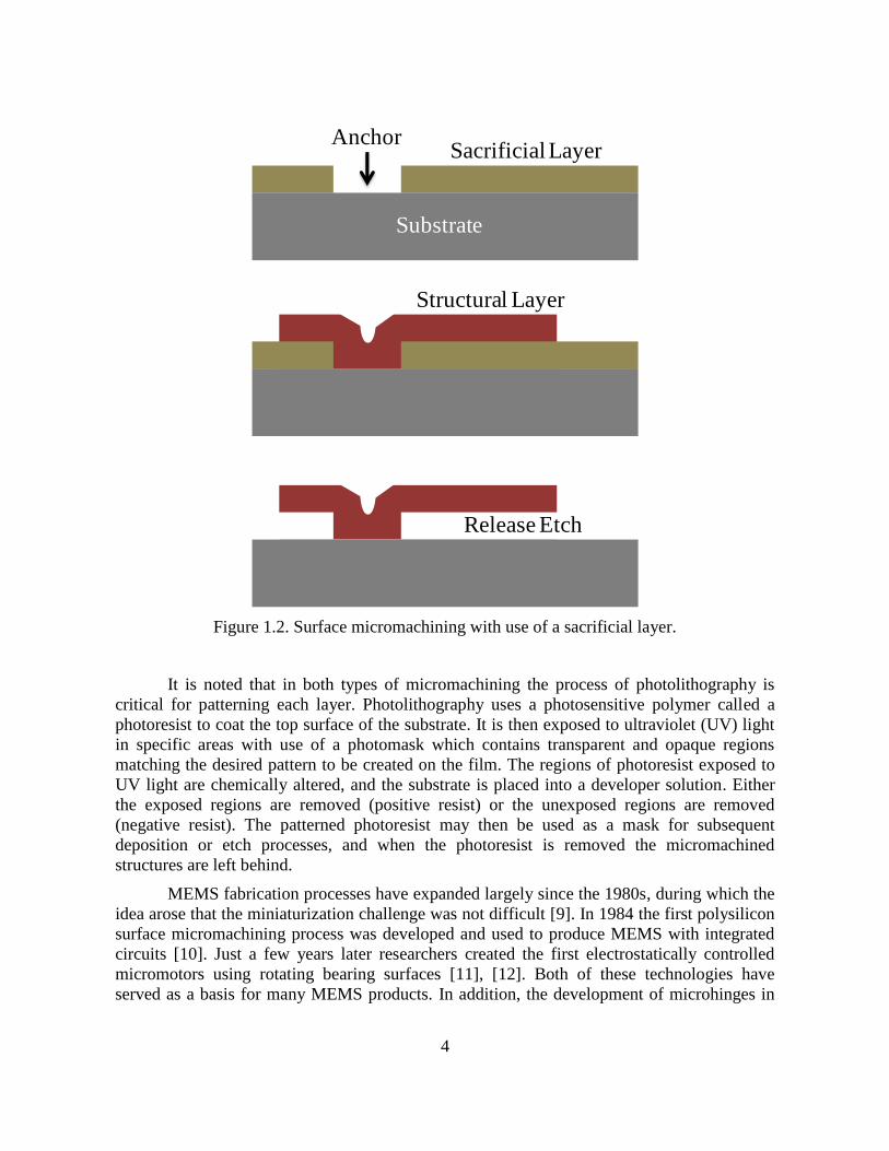
sequence. Both BMM and SMM techniques are illustrated below in Figure 1.1 and Figure 1.2,
respectively.

3
Silicon Wafer
Doped Silicon
Hard Mask Material
Anisotropic Etching
Membrane V-GrooveThrough
Hole
Figure 1.1. Bulk micromachining using anisotropic etching.
4
Substrate
AnchorSacrificial Layer
Structural Layer
Release Etch
Figure 1.2. Surface micromachining with use of a sacrificial layer.
It is noted that in both types of micromachining the process of photolithography is
critical for patterning each layer. Photolithography uses a photosensitive polymer called a
photoresist to coat the top surface of the substrate. It is then exposed to ultraviolet (UV) light
in specific areas with use of a photomask which contains transparent and opaque regions
matching the desired pattern to be created on the film. The regions of photoresist exposed to
UV light are chemically altered, and the substrate is placed into a developer solution. Either
the exposed regions are removed (positive resist) or the unexposed regions are removed
(negative resist). The patterned photoresist may then be used as a mask for subsequent
deposition or etch processes, and when the photoresist is removed the micromachined
structures are left behind.
MEMS fabrication processes have expanded largely since the 1980s, during which the
idea arose that the miniaturization challenge was not difficult [9]. In 1984 the first polysilicon
surface micromachining process was developed and used to produce MEMS with integrated
circuits [10]. Just a few years later researchers created the first electrostatically controlled
micromotors using rotating bearing surfaces [11], [12]. Both of these technologies have
served as a basis for many MEMS products. In addition, the development of microhinges in
5
1991 extended surface micromachining of polysilicon such that large structure could be
assembled out of plane relative to the substrate [13]. This third dimensional aspect led to an
incredible increase in the number of devices, technologies, and applications in the field of
MEMS.
1.3 Packaging
Packaging is highly critical for the practical realization of MEMS devices, often being
the most costly step in the manufacturing process [14]. Packaging is also important for yield
and reliability [15]. Both the encapsulation of the moving, working parts of the device and the
electrical interconnection must be integrated into the fabrication method for the MEMS
devices. The MEMS device must essentially be sealed within a protective cap. In addition,
there may be specific performance-related packaging requirements. MEMS devices such as
pressure sensors or chemical/fluidic sensors need to be exposed to the environment to
function. On the other hand, accelerometers, gyroscopes, and oscillators may need to be
hermetically sealed, sometimes with an anti-stiction agent and/or buffer gas [16]. Overall, the
delicate, specific, and varied nature of MEMS devices can complicate the integration of
packaging steps and drive up manufacturing costs. Due to the widely varying conditions and
specifications for MEMS packaging, no single universal packaging method exists. A sample
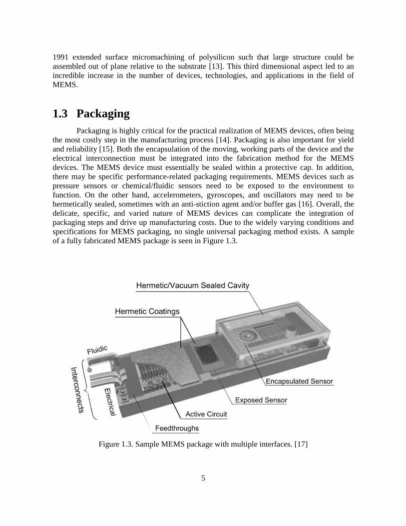
of a fully fabricated MEMS package is seen in Figure 1.3.
Figure 1.3. Sample MEMS package with multiple interfaces. [17]

6
1.4 Dissertation Overview
The motivation for this work lies in the pursuit of a broadly applicable MEMS
packaging scheme for large area devices using a streamlined fabrication process. First the
necessary background, criteria, and design considerations for MEMS packaging are discussed
in Chapter 2. Two approaches to wafer level packaging, interfacial bonding (bulk
micromachining) and thin film encapsulation (surface micromachining) are evaluated in the
context of simplified fabrication and cost effectiveness. Chapters 3 and 4 test and present the
potential of two different thin film encapsulation technologies, seen below in Figure 1.4
Figure 1.4. Schematic diagrams for thin film encapsulation using: (a) permeable polysilicon,
and (b) composites of carbon nanotubes and polysilicon.
7
In Chapter 3 a thin film encapsulation method using permeable polysilicon for MEMS
devices is presented, as seen in Figure 1.4(a). The necessary process parameters to render the
thin polysilicon film permeable are developed. Furthermore, the encapsulation membrane is
modeled to determine the necessary thickness of the sealing layer to sustain the package
against atmospheric pressure loading. This requires supplemental material deposited on top of
the permeable membrane. Therefore, a process of incremental thick oxide deposition and
thermal annealing is optimized to hasten both the seal of the membrane and necessary filling
of sacrificial oxide beneath the thin film package.
This process evolves in Chapter 4 into using polysilicon as a filler material in a
composite membrane formed by carbon nanotubes (CNTs), shown in Figure 1.4(b). The
CNTs serve as a skeletal framework for the membrane, which contains a natural permeability
due to its porosity. This structure is used to expand beyond thickness limitations of typical
thin film approaches while offering the advantages in packaging via surface micromachining.
The CNT/polysilicon composite membrane is modeled for deflection under load to assist with
designing thickness for any given area. In addition, the permeability and etching behavior of
the sacrificial underlayer are characterized.
Chapter 5 summarizes the work in this dissertation and suggests future directions to
further assess the viability of the CNT/polysilicon composite membrane and implement it into
practical applications.
8
Chapter 2
MEMS Packaging Overview
2.1 Background
2.1.1 Packaging Considerations
Broadly speaking the main functions of MEMS packaging are as follows:
1. Mechanical sustentation – the packaging material should sustain and protect the
internal MEMS devices from the working environment. This may include
protection against shock due to impact. Material selection plays a very important
role, and in some cases glass or ceramic packages are attractive for their insulating
and hermetic properties [18]. Moreover, the coefficient of thermal expansion (CTE)
plays a significant factor in selecting packaging materials to minimize mechanical
thermal stress at the interface between the MEMS die and the package substrate.
2. Protection from environment – embedded MEMS devices on a die should be
electrically isolated or passivated from electrolytes and moisture. This is extremely
important because moisture, which may come from humidity in the environment,
can cause corrosion of the device and hamper performance. Metal interconnects
also are susceptible to becoming disconnected due to environmental factors.
3. Electrical connection –MEMS devices require electrical connections to the outside
world, and this is a significant consideration for designing the packaging process
steps. One benefit is that the signal path within the MEMS device is typically short
and electrical noise may be unlikely or less impactful.
4. Thermal budgets – One of the greatest limitations in packaging is the temperature of
the process steps. In addition to the above mentioned CTE and its effect on
inducing stress at the die/package interface, many IC devices have a thermal budget
based on the allowed dopant diffusion. Repeated high temperature steps may
destroy the diffusion profile for CMOS devices, especially, aluminum can begin to
spike into devices at temperatures as low as 400°C [19].
The two general approaches to packaging MEMS are at the die level and the wafer
level. In the die level approach chips are fully fabricated, diced, then sealed or packaged
individually. On the other hand, wafer level packaging consolidates the sealing and testing
9
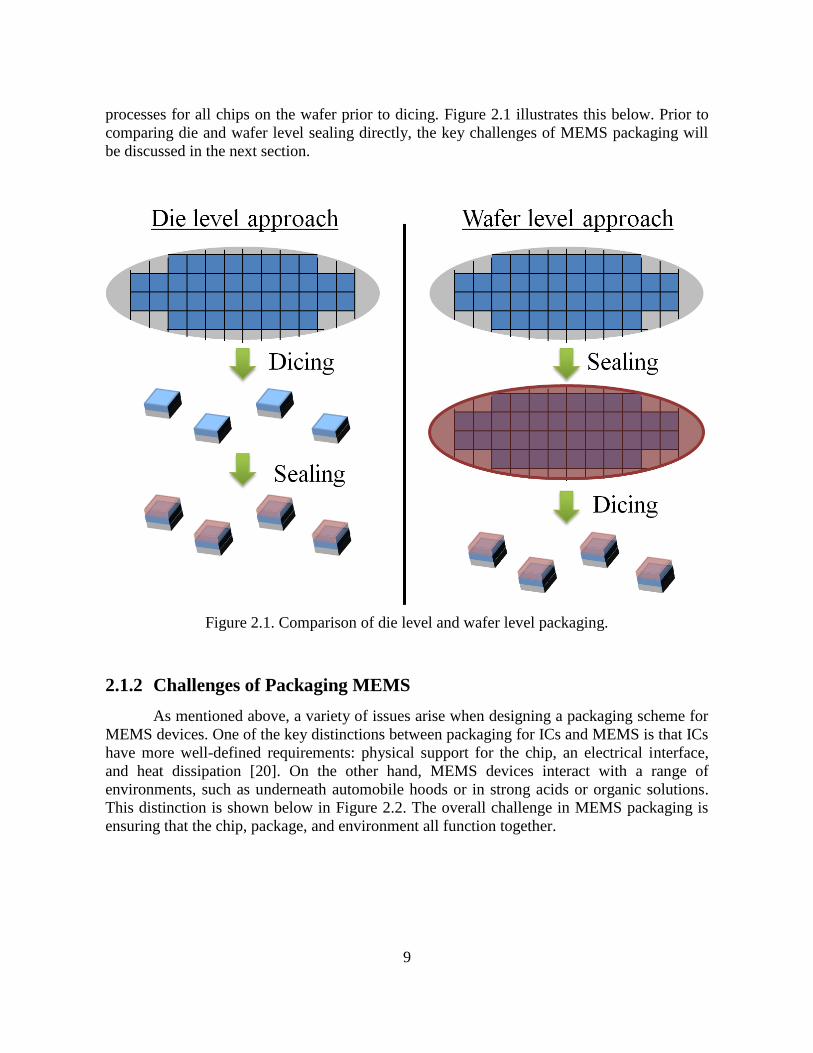
processes for all chips on the wafer prior to dicing. Figure 2.1 illustrates this below. Prior to
comparing die and wafer level sealing directly, the key challenges of MEMS packaging will
be discussed in the next section.
Figure 2.1. Comparison of die level and wafer level packaging.
2.1.2 Challenges of Packaging MEMS
As mentioned above, a variety of issues arise when designing a packaging scheme for
MEMS devices. One of the key distinctions between packaging for ICs and MEMS is that ICs
have more well-defined requirements: physical support for the chip, an electrical interface,
and heat dissipation [20]. On the other hand, MEMS devices interact with a range of
environments, such as underneath automobile hoods or in strong acids or organic solutions.
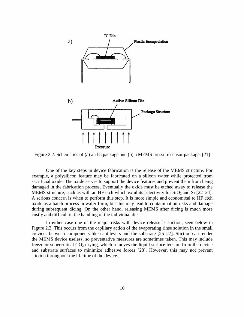
This distinction is shown below in Figure 2.2. The overall challenge in MEMS packaging is
ensuring that the chip, package, and environment all function together.
10
a)
b)
Figure 2.2. Schematics of (a) an IC package and (b) a MEMS pressure sensor package. [21]
One of the key steps in device fabrication is the release of the MEMS structure. For
example, a polysilicon feature may be fabricated on a silicon wafer while protected from
sacrificial oxide. The oxide serves to support the device features and prevent them from being
damaged in the fabrication process. Eventually the oxide must be etched away to release the
MEMS structure, such as with an HF etch which exhibits selectivity for SiO2 and Si [22–24].
A serious concern is when to perform this step. It is more simple and economical to HF etch
oxide as a batch process in wafer form, but this may lead to contamination risks and damage
during subsequent dicing. On the other hand, releasing MEMS after dicing is much more
costly and difficult in the handling of the individual dies.
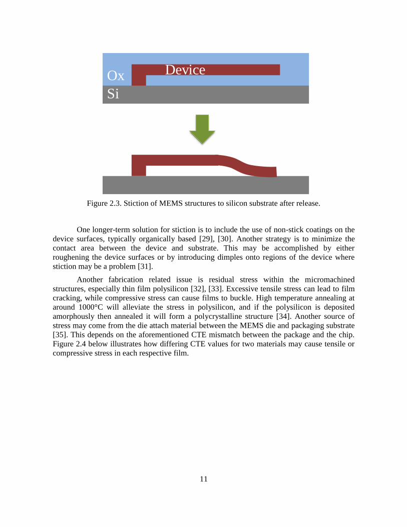
In either case one of the major risks with device release is stiction, seen below in
Figure 2.3. This occurs from the capillary action of the evaporating rinse solution in the small
crevices between components like cantilevers and the substrate [25–27]. Stiction can render
the MEMS device useless, so preventative measures are sometimes taken. This may include
freeze or supercritical CO2 drying, which removes the liquid surface tension from the device
and substrate surfaces to minimize adhesive forces [28]. However, this may not prevent
stiction throughout the lifetime of the device.
11
Si
Ox Device
Figure 2.3. Stiction of MEMS structures to silicon substrate after release.
One longer-term solution for stiction is to include the use of non-stick coatings on the
device surfaces, typically organically based [29], [30]. Another strategy is to minimize the
contact area between the device and substrate. This may be accomplished by either
roughening the device surfaces or by introducing dimples onto regions of the device where
stiction may be a problem [31].
Another fabrication related issue is residual stress within the micromachined
structures, especially thin film polysilicon [32], [33]. Excessive tensile stress can lead to film
cracking, while compressive stress can cause films to buckle. High temperature annealing at
around 1000°C will alleviate the stress in polysilicon, and if the polysilicon is deposited
amorphously then annealed it will form a polycrystalline structure [34]. Another source of
stress may come from the die attach material between the MEMS die and packaging substrate
[35]. This depends on the aforementioned CTE mismatch between the package and the chip.
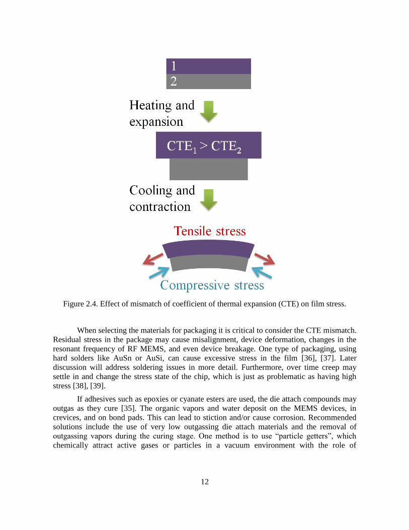
Figure 2.4 below illustrates how differing CTE values for two materials may cause tensile or
compressive stress in each respective film.
12
Figure 2.4. Effect of mismatch of coefficient of thermal expansion (CTE) on film stress.
When selecting the materials for packaging it is critical to consider the CTE mismatch.
Residual stress in the package may cause misalignment, device deformation, changes in the
resonant frequency of RF MEMS, and even device breakage. One type of packaging, using
hard solders like AuSn or AuSi, can cause excessive stress in the film [36], [37]. Later
discussion will address soldering issues in more detail. Furthermore, over time creep may
settle in and change the stress state of the chip, which is just as problematic as having high
stress [38], [39].
If adhesives such as epoxies or cyanate esters are used, the die attach compounds may
outgas as they cure [35]. The organic vapors and water deposit on the MEMS devices, in
crevices, and on bond pads. This can lead to stiction and/or cause corrosion. Recommended
solutions include the use of very low outgassing die attach materials and the removal of
outgassing vapors during the curing stage. One method is to use “particle getters”, which
chemically attract active gases or particles in a vacuum environment with the role of

13
maintaining and even improving vacuum [40], [41]. This may prolong the operational lifetime
of sealed MEMS packages.
As mentioned above another consideration is dicing the wafer into individual chips.
This process usually involves a diamond saw and requires coolant to flow over the surface of
the wafer. The coolant may combine with silicon and diamond particles to contaminate the
devices [42], [43]. One way around this is to cleave the wafers with a laser, but this process
may result in thermal damage to the chips [44].
One difference between the assembly of MEMS and IC dies is that MEMS dice
typically require special handling. This is due to the delicate surface features of the MEMS
structures, and unlike IC dies they may not be moved using vacuum pick-up heads. Instead,
MEMS dice must be picked up and handled by the edges by fixtures such as fingers or
clamps. This is more difficult than handling dies by an entire surface due to the reduced area
and increased dexterity requirements of pick and place equipment [45].
Wafer level encapsulation, on the other hand, eliminates the need for special die
handling fixtures. Since a capping wafer is bonded to the top of a device wafer and when
diced, each MEMS chip has a protective lid attached to it already. In addition, these wafers
may be bonded in a vacuum to produce a permanent vacuum or low pressure environment
inside each device chip. Various types of wafer level packaging are discussed in the following
section. Finally, Table 2.1 below summarizes MEMS packaging issues and recommended
solutions in this section.
Table 2.1. Summary of packaging parameters, challenges, and solutions for MEMS.
Packaging
Parameters
Challenge Solutions
Release and
stiction
Stiction of devices Freeze drying, CO2 drying, roughening
of contact surfaces, non-stick coatings
Stress Performance degradation,
resonant frequency shifts,
failure
Low modulus die attach, annealing,
minimize CTE mismatch
Outgassing Stiction, corrosion Low outgassing epoxies, low modulus
solders, removal of outgassing vapors
Dicing Contamination risks Release devices after dicing, flush chip
surface to remove contaminants, wafer
cleaving with lasers
Die handling Device failure, top die face
sensitive to contact/exposure
Edge-holding fixtures, wafer level
encapsulation
14
2.2 Wafer Level Packaging
2.2.1 Overview of Wafer Level Processes
In the context of the previously addressed issues for MEMS devices, wafer level
encapsulation presents a variety of appealing characteristics for large volume MEMS
fabrication. Most importantly, there are substantially potential lower costs and higher volume
throughput in wafer level packaging relative to the component or die level approach [46]. In
addition, wafer level packaging enables device testing during batch fabrication. This may save
costs and time compared to packaging individual dies because in the latter approach the
testing only occurs after all devices have been fully diced and sealed.
Sealing the MEMS within their cavities earlier in the fabrication process protects them
mechanically. Moreover, this wafer level packaging limits contamination during fabrication
steps such as dicing, since there is a seal ring surrounding each die that will enclose it from
byproducts of that or any other process. Batch encapsulation may also eliminate the need for
extra packaging equipment. For example, wafer level packaged pressure sensors could be
calibrated via reference pressure chambers.
The ability to miniaturize low cost microsensor applications and integrate them with
other systems is another driving force behind the industry shift towards wafer level packaging
[47]. Yet, a definitive industry-wide standard remains elusive due to the wide variety of
applications for MEMS devices, from implantable biological sensors to RF wireless
communications. Before delving further it is necessary to examine different types of wafer
level packaging, as follows in the next sections.
2.2.2 Interfacial Bonding
This method essentially involves using an external lid as a physical shell or capsule
that may be placed over sensitive parts of the MEMS device, as seen below in Figure 2.5.
There are three essential aspects of the entire package: the capsule, feedthroughs for signal
transfer, and the bonding interface between the sealing layer and the device substrate. The
capsule may be fabricated from a variety of materials, such as metals, glass/ceramics, silicon,
or other semiconductor materials [48]. As discussed before, the capsule must be bonded to the
device substrate prior to dicing in order to minimize handling costs and protect the MEMS
components from subsequent process steps.

15
Figure 2.5. Cross section of an interfacial capsule or shell bonded to a substrate. [17]
During the bonding process high temperatures should be avoided to prevent damage to
both the MEMS components and the interconnection. Moreover, the surface of the MEMS
substrate should be planar enough so that the bond interface between the two substrates may
be atomically close. As a result bonding silicon to silicon is not a good option because
temperatures may exceed 1000°C in the standar silicon-to-silicon fusion bonding process
[49].
Whatever the chosen capsule material may be, such as glass or solder, the primary
goal is a permanent seal which will provide a long-term, stable hermetic or vacuum
environment for the MEMS device. Most of these packages tend to be resistant to permeation
by various gases or other environmental conditions like moisture [48]. Finally, it is sometimes
easier to fabricate the signal feedthrough on the capsule substrate instead of the device
substrate, since the surface of the MEMS chip may either be delicate, nonplanar, or otherwise
constricted.
One of the more widely used bonding methods in MEMS is that between a glass
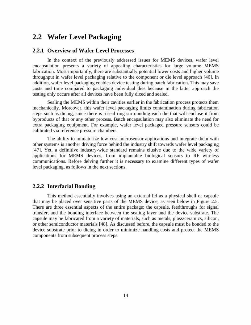
capsule (usually Pyrex 7740) and a silicon substrate in a process called anodic, or
electrostatic, bonding [50–52]. Figure 2.6 illustrates the anodic bonding setup and mechanism
of ion drift that causes chemical bonds to form at the interface.
16
Chuck
Si wafer
Pyrex wafer
Top tool
Bond electrode
IB
VB
Na+
Na+Na+
O-O- O-
Bond interface
E
a) b)
Figure 2.6. Anodic bonding schematic showing (a) procedure with top tool functioning as a
cathode and the chuck as an anode, and (b) ion drift in the Pyrex glass as a result of the
electric field, forming a depletion zone at the interface to which O- ions drift.
In this process the two substrates come into intimate contact, are heated to roughly
400°C, and then experience a voltage from 800-1500V across the interface. This generates a
large electrostatic attractive force to promote a chemical bond between the substrates.
Specifically, Si and O2 atoms form a Si-O bond that is stronger than both an Si-Si bond and
glass [53]. After the bond forms the package cools to room temperature. One of the reasons
Pyrex 7740 glass is a standard capsule material for anodic bonding to silicon is that the CTE
mismatch is very low from room temperature to 400°C [54].
There are other advantages to using glass a capsule, the most apparent one being
transparency. This allows such packages to be used for Micro-Opto-Electromechanical
Systems (MOEMS) and biomedical applications in which a radio frequency signal must be
transmitted to the embedded device [55–59]. Furthermore, Pyrex 7740 is biocompatible and
resistant to corrosive environments such as salt water or humidity. Since glass wafer
technology is well established, material costs can be kept low.
Other methods of interfacial bonding include silicon-gold eutectic bonding, glass frit
bonding, fusion bonding, and evaporated glass bonding [60–64]. Wafer bonding with solder
or eutectics is one of the more common approaches. A solder forms in the bond area between
the package and device substrates. After the substrates are brought together, the temperature is
raised to produce solder reflow which forms the bond. This heating may be localized with
induction heating using magnetic coils, such that the MEMS device temperature may remain
less than 125°C [65]. However, solder materials may contain impurities which cause them to
outgas during the reflow process, creating problems for vacuum packaging [66], [67].
Eutectic soldering, on the other hand, employs the use of a metal such as gold to form
a bond between the device and package substrates [68], [69]. The silicon-gold eutectic is
attractive because it forms at a temperature of roughly 360°C. Outgassing is not a problem

17
because the mixture forms from simply raising the temperature and the starting materials are
pure, unlike solder. The low temperature is sufficient for most MEMS applications. Figure 2.7
below shows the mechanism and experimental setup for eutectic bonding using gold to a
silicon capsule.
Figure 2.7. Schematic diagram of Au-Si eutectic bonding for packaging a silicon cap wafer to
a MEMS device wafer, (a) before bonding and (b) after bonding. [62]
The eutectic may be used to bond two wafers or for hermetic and vacuum packaging.
Usually the gold is deposited onto the sealing substrate, and the silicon is provided from the
bulk of the device substrate or a thin film deposited on one or both of the wafers. Once the
two materials are brought into contact and heated above the eutectic temperature, the liquid
mixture forms by silicon diffusing into the gold. Once cooled a strong diffusional bond forms
at the interface [70].
One of the issues with Si-Au eutectic bonding is the lack of uniformity and
reproducibility. There are various reasons for this, including non-uniform eutectic flow, void
formation, insufficient eutectic material between wafers that causes non-uniform bonding,
oxidation of bond surfaces, and poor surface contact or adhesion [71]. The quality of the Au-
Si bond may be improved by conducting the process in a vacuum or inert gas ambient to
avoid oxidation at high temperature. In addition, the bonding surface should be clean and
18
smooth. During bonding a contact force should be applied to the wafers, and cooling should
occur as quickly as possible. To ensure sufficient coverage of the Au-Si eutectic on the
interface, the eutectic material should be several μm thick so that it covers nonplanar surfaces.
Lastly, the wafers may be baked to minimize outgassing [72].
While Au-Si eutectic bonding has a process temperature less than 400°C when using a
silicon cap, the temperature must be raised if another material such as glass frit is used [73],
[74]. Temperatures of 700°C and above begin to exceed the allowable range for various
MEMS devices as well as ICs. Furthermore, some MEMS devices incorporate polymers or
biological coatings which cannot withstand temperatures much greater than 100°C [75].
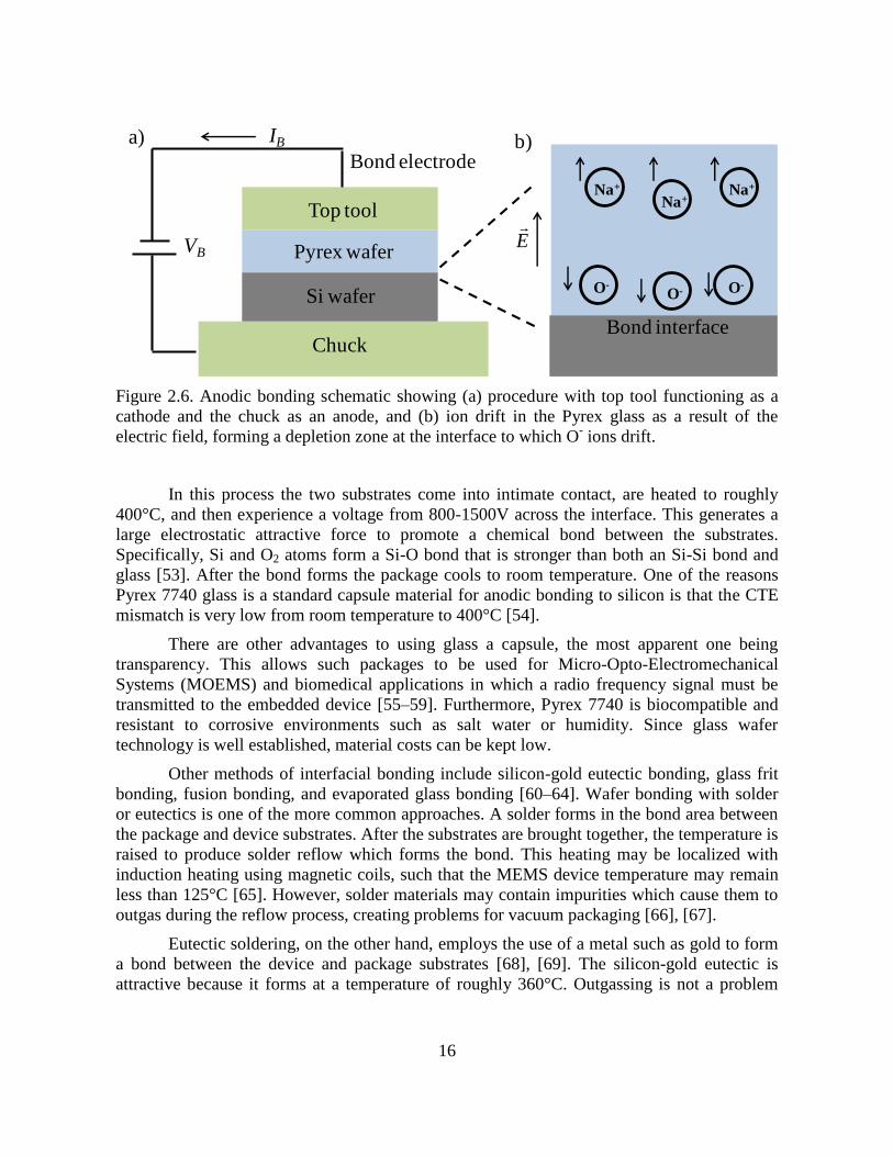
As mentioned for soldering, localized heating is useful to avoid damaging the MEMS
device with high bonding temperatures. Several techniques have been developed, such as
microwave heating, laser heating, localized CVD deposition, resistive heating, ultrasonic
bonding, and RF heating [76–83]. An example of localized heating using on-chip resistors is
seen below in Figure 2.8.
Figure 2.8. Schematic of localized bonding using on-chip resistors. [17]
The resistive heater may be used with common materials such as aluminum or
polysilicon. In addition, it may be patterned onto either the sealing substrate or the device
substrate. Silicon has a good thermal conductivity of 149 W/m-K, enabling heat from the
resistive heater to be confined and localized to the bonding area. Sensitive regions of the
device substrate may be maintained at room temperature or slightly above by using a heat
sink. For example, the temperature can vary from over 700°C to 50°C over a length of 100μm
or less [17]. However, the entire package may be baked at an elevated temperature to allow
for outgassing of any residual materials on either the package surface or the device substrate.
19
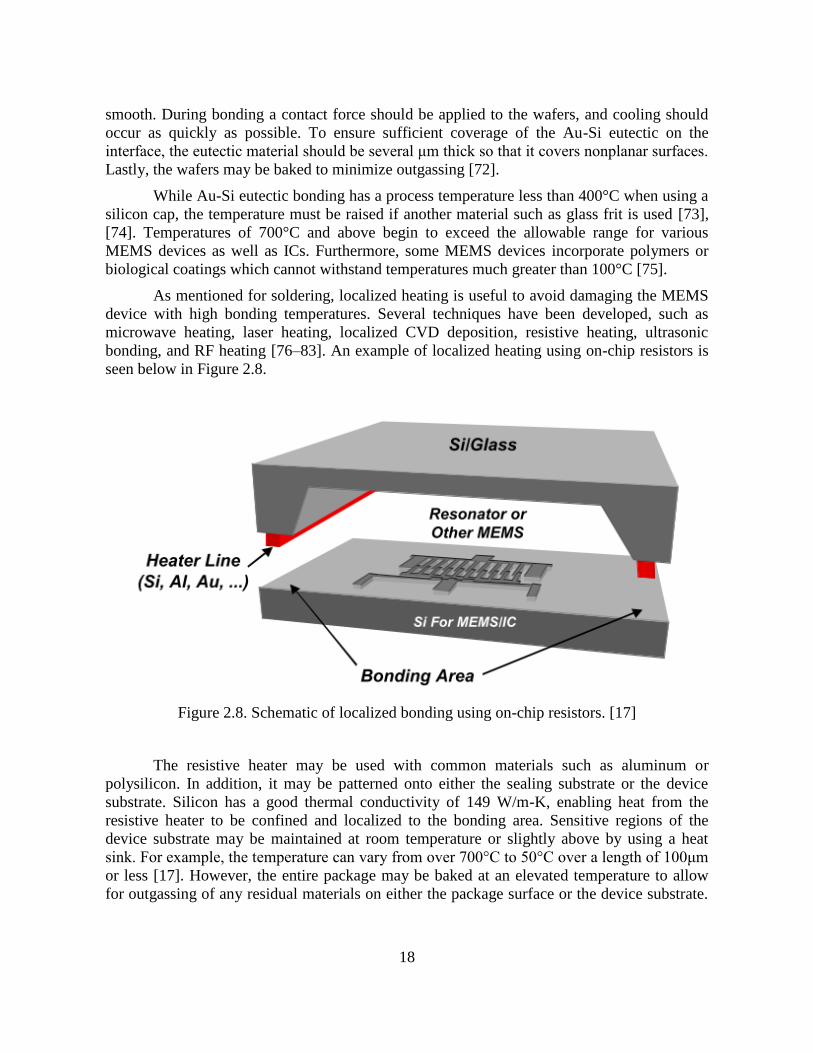
Additional protective layers such as Ti/Pt may be implemented on the inside of the glass cap
to prevent future outgassing and also function as a getter, which absorbs residual outgassing
within the package [84]. Figure 2.9 shows an example of a microresonator which has been
encapsulated using localized bonding between aluminum and the glass cap.
Figure 2.9. SEM photograph of an encapsulated microresonator under a glass cap. [84]
Overall, localized heating for bonding is very attractive for highly sensitive MEMS
devices. A variety of materials may be used in the bonding region. They will conform to the
topology of the substrate which may often be nonplanar due to the implementation of
electrical feedthroughs which carry signals between the sealed device and the outside
environment.
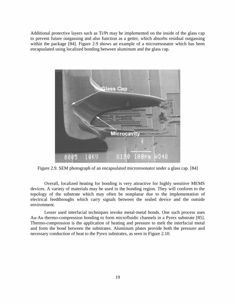
Lesser used interfacial techniques invoke metal-metal bonds. One such process uses
Au-Au thermo-compression bonding to form microfluidic channels in a Pyrex substrate [85].
Thermo-compression is the application of heating and pressure to melt the interfacial metal
and form the bond between the substrates. Aluminum plates provide both the pressure and
necessary conduction of heat to the Pyrex substrates, as seen in Figure 2.10.
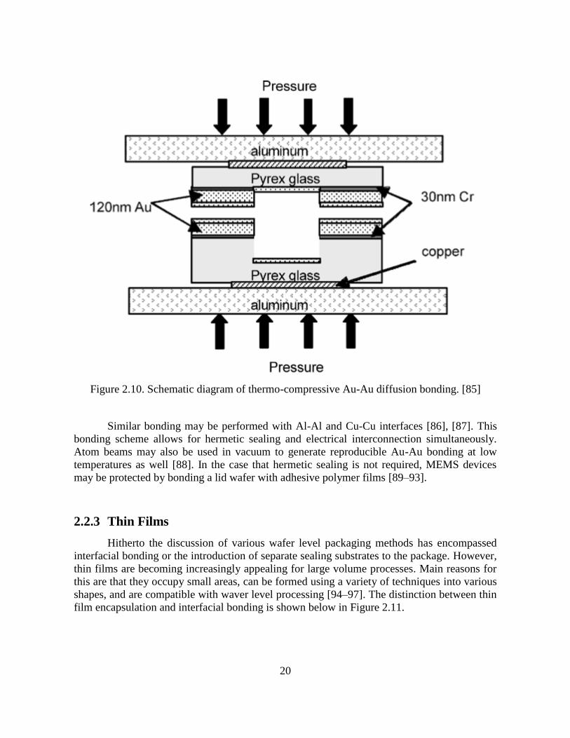
20
Figure 2.10. Schematic diagram of thermo-compressive Au-Au diffusion bonding. [85]
Similar bonding may be performed with Al-Al and Cu-Cu interfaces [86], [87]. This
bonding scheme allows for hermetic sealing and electrical interconnection simultaneously.
Atom beams may also be used in vacuum to generate reproducible Au-Au bonding at low
temperatures as well [88]. In the case that hermetic sealing is not required, MEMS devices
may be protected by bonding a lid wafer with adhesive polymer films [89–93].
2.2.3 Thin Films
Hitherto the discussion of various wafer level packaging methods has encompassed
interfacial bonding or the introduction of separate sealing substrates to the package. However,
thin films are becoming increasingly appealing for large volume processes. Main reasons for
this are that they occupy small areas, can be formed using a variety of techniques into various
shapes, and are compatible with waver level processing [94–97]. The distinction between thin
film encapsulation and interfacial bonding is shown below in Figure 2.11.
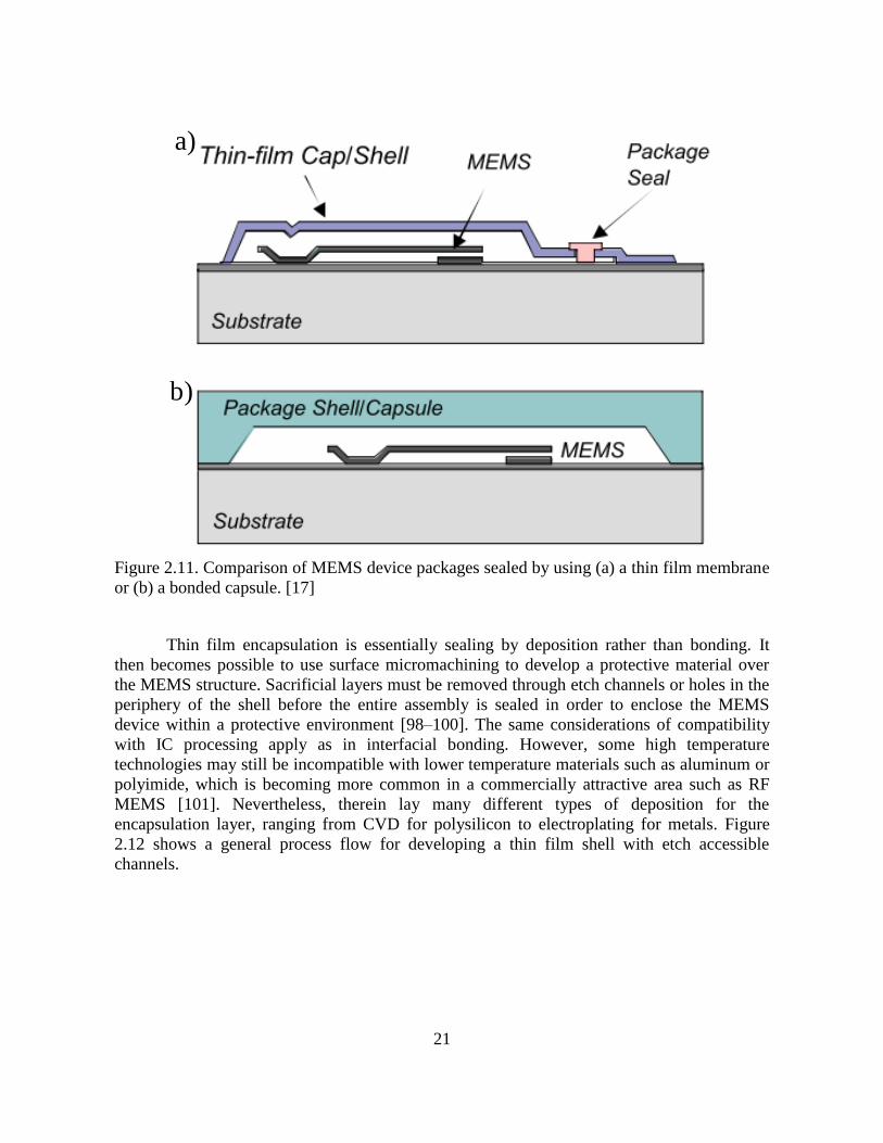
21
b)
a)
Figure 2.11. Comparison of MEMS device packages sealed by using (a) a thin film membrane
or (b) a bonded capsule. [17]
Thin film encapsulation is essentially sealing by deposition rather than bonding. It
then becomes possible to use surface micromachining to develop a protective material over
the MEMS structure. Sacrificial layers must be removed through etch channels or holes in the
periphery of the shell before the entire assembly is sealed in order to enclose the MEMS
device within a protective environment [98–100]. The same considerations of compatibility
with IC processing apply as in interfacial bonding. However, some high temperature
technologies may still be incompatible with lower temperature materials such as aluminum or
polyimide, which is becoming more common in a commercially attractive area such as RF
MEMS [101]. Nevertheless, therein lay many different types of deposition for the
encapsulation layer, ranging from CVD for polysilicon to electroplating for metals. Figure
2.12 shows a general process flow for developing a thin film shell with etch accessible
channels.
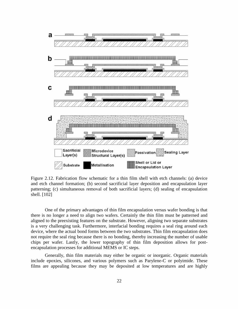
22
Figure 2.12. Fabrication flow schematic for a thin film shell with etch channels: (a) device
and etch channel formation; (b) second sacrificial layer deposition and encapsulation layer
patterning; (c) simultaneous removal of both sacrificial layers; (d) sealing of encapsulation
shell. [102]
One of the primary advantages of thin film encapsulation versus wafer bonding is that
there is no longer a need to align two wafers. Certainly the thin film must be patterned and
aligned to the preexisting features on the substrate. However, aligning two separate substrates
is a very challenging task. Furthermore, interfacial bonding requires a seal ring around each
device, where the actual bond forms between the two substrates. Thin film encapsulation does
not require the seal ring because there is no bonding, thereby increasing the number of usable
chips per wafer. Lastly, the lower topography of thin film deposition allows for post-
encapsulation processes for additional MEMS or IC steps.
Generally, thin film materials may either be organic or inorganic. Organic materials
include epoxies, silicones, and various polymers such as Parylene-C or polyimide. These
films are appealing because they may be deposited at low temperatures and are highly
23
conformal [103]. In addition, the properties of organic materials may be tuned for different
applications. However, most organics tend to be porous and are prone to moisture penetration.
As mentioned earlier this is acceptable provided that the particular MEMS device does not
require a hermetic seal. However, for those devices needing to perform in harsh environments
organic thin films may not be a good choice. Nevertheless, these materials may still be used
for applications that do not require long-term operation, for which environmental conditions
may be controlled, or where performance specifications are not too rigid. In the absence of
strict hermetic or vacuum requirements, polymers make excellent thin film choices.
On the other hand, a wide range of inorganic materials may be used for thin film
packaging. Examples are silicon nitride, silicon carbide, polycrystalline diamond, metal thin
films, or other environmentally resistant materials [104–106]. These materials are attractive
because they exhibit varying degrees of resistance to corrosive environments. However, they
typically require higher temperatures to attain reasonable deposition rates. In some instances
the films are not as conformal as required, such as in the case where post-encapsulation
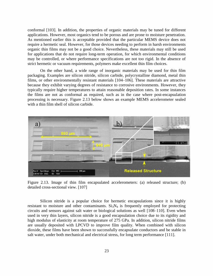
processing is necessary. Figure 2.13 below shows an example MEMS accelerometer sealed
with a thin film shell of silicon carbide.
Figure 2.13. Image of thin film encapsulated accelerometers: (a) released structure; (b)
detailed cross-sectional view. [107]
Silicon nitride is a popular choice for hermetic encapsulations since it is highly
resistant to moisture and other contaminants. Si3N4 is frequently employed for protecting
circuits and sensors against salt water or biological solutions as well [108–110]. Even when
used in very thin layers, silicon nitride is a good encapsulation choice due to its rigidity and
high modulus of elasticity at room temperature of 275 GPa. In addition, silicon nitride films
are usually deposited with LPCVD to improve film quality. When combined with silicon
dioxide, these films have been shown to successfully encapsulate conductors and be stable in
salt water, under both mechanical and electrical stress, for long term performance [111].
24
Thin metal films are also suitable for hermetic MEMS packaging [112], [113]. They
provide a strong barrier against moisture and may be deposited onto a polymer or other
organic film [114]. This provides electrical isolation between the metal film and the devices
being encapsulated. However, caution must be taken in selecting the polymeric film, as the
thickness and dielectric constant will affect the parasitic capacitance from the circuitry to the
package. This may limit the frequency response of integrated electronics within the MEMS
device. The polymer must also have good adhesion to metal and cure at a temperature that
exceeds the thermal budget of following process steps to prevent the polymer from bubbling.
One reliable choice is polyimide, which has a low dielectric constant and may be spun cast
into thick films that cure above 350°C [115]. The metal itself, such as gold, may be deposited
via sputtering, evaporation, or electroplating. Gold is popular for its biocompatibility and ease
of electroplating.
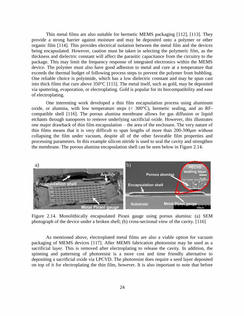
One interesting work developed a thin film encapsulation process using aluminum
oxide, or alumina, with low temperature steps (< 300°C), hermetic sealing, and an RF-
compatible shell [116]. The porous alumina membrane allows for gas diffusion or liquid
etchants through nanopores to remove underlying sacrificial oxide. However, this illustrates
one major drawback of thin film encapsulation – the area of the enclosure. The very nature of
thin films means that it is very difficult to span lengths of more than 200-300μm without
collapsing the film under vacuum, despite all of the other favorable film properties and
processing parameters. In this example silicon nitride is used to seal the cavity and strengthen
the membrane. The porous alumina encapsulation shell can be seen below in Figure 2.14.
a) b)
Figure 2.14. Monolithically encapsulated Pirani gauge using porous alumina: (a) SEM
photograph of the device under a broken shell; (b) cross-sectional view of the cavity. [116]
As mentioned above, electroplated metal films are also a viable option for vacuum
packaging of MEMS devices [117]. After MEMS fabrication photoresist may be used as a
sacrificial layer. This is removed after electroplating to release the cavity. In addition, the
spinning and patterning of photoresist is a more cost and time friendly alternative to
depositing a sacrificial oxide via LPCVD. The photoresist does require a seed layer deposited
on top of it for electroplating the thin film, however. It is also important to note that before

25
these steps feedthroughs and etch channels should be fabricated. Figure 2.15 below shows the
process flow for creating a thin film package of electroplated metal such as nickel.
Figure 2.15. Fabrication process for creating electroplated nickel vacuum packages. [117]
Lastly, polysilicon is a viable material for vacuum packaging of various resonators,
gyroscopes and other MEMS devices often fabricated of polysilicon themselves [118–120].
Details of using polysilicon as a thin film encapsulation material are discussed in the
following chapter. Polysilicon may also be used as a sacrificial layer for releasing MEMS
structures by using passivation techniques, such as with silicon dioxide [121]. Furthermore,
polysilicon film may be grown epitaxially via CVD from a thin seed layer to hasten
processing time for developing thicker encapsulation layers [122], [123]. Figure 2.16 shows
how this film is created.
Figure 2.16. Schematic of fabrication process for epitaxial polysilicon encapsulation. [122]

26
The hermeticity of the thick polysilicon film varies depending on which type of gas
tested. Specifically, the thick polysilicon film was permeable to hydrogen and helium but not
nitrogen or argon. This can be advantageous for pressure management of the cavity depending
on the application. For example, some inertial sensors may require some pressure to dampen
signals. Overall, polysilicon is one of many useful thin film materials that may be used for
vacuum sealing of MEMS devices.
2.2.4 Electrical Feedthrough
While discussed in context of the previous section’s fabrication methods, it is
important to consider that electrical feedthrough is required for interconnection between the
sealed MEMS device and the outside environment with which it interacts. Typically the
feedthrough is incorporated with the wafer level encapsulation process. For interfacial
bonding the feedthrough should be fabricated before sealing the device cavity, while for thin
film sealing interconnects are developed simultaneously and/or possibly during post-
encapsulation. Normally metal is used as the feedthrough material, but highly doped silicon
may also apply [124]. Metal has low resistance and high conductivity, while silicon will have
the same CTE as the underlying substrate.
The first type of interconnection is lateral feedthrough [125]. An example of this
process is shown below in Figure 2.17, which uses spin on glass (SOG) as a top layer oxide.
Si
Oxide
Cr
Al
SOG
Si
Pyrex glass
a)
b)
c)
d)
e)
f)
Figure 2.17. Lateral feedthrough process flow for anodic bonding: (a) pattern oxide; (b)
deposit metal; (c) lift-off; (d) SOG coating; (e) Si sputtering; (f) Pyrex cap anodic bonding.
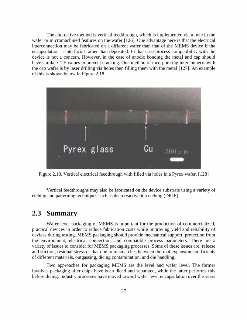
27
The alternative method is vertical feedthrough, which is implemented via a hole in the
wafer or micromachined features on the wafer [126]. One advantage here is that the electrical
interconnection may be fabricated on a different wafer than that of the MEMS device if the
encapsulation is interfacial rather than deposited. In that case process compatibility with the
device is not a concern. However, in the case of anodic bonding the metal and cap should
have similar CTE values to prevent cracking. One method of incorporating interconnects with
the cap wafer is by laser drilling via holes then filling them with the metal [127]. An example
of this is shown below in Figure 2.18.
Figure 2.18. Vertical electrical feedthrough with filled via holes in a Pyrex wafer. [128]
Vertical feedthroughs may also be fabricated on the device substrate using a variety of
etching and patterning techniques such as deep reactive ion etching (DRIE).
2.3 Summary
Wafer level packaging of MEMS is important for the production of commercialized,
practical devices in order to reduce fabrication costs while improving yield and reliability of
devices during testing. MEMS packaging should provide mechanical support, protection from
the environment, electrical connection, and compatible process parameters. There are a
variety of issues to consider for MEMS packaging processes. Some of these issues are: release
and stiction, residual stress or that due to mismatches between thermal expansion coefficients
of different materials, outgassing, dicing contamination, and die handling.
Two approaches for packaging MEMS are die level and wafer level. The former
involves packaging after chips have been diced and separated, while the latter performs this
before dicing. Industry processes have moved toward wafer level encapsulation over the years
28
due to substantially lower costs and higher volume throughput. Miniaturization of sensors and
actuators has also piqued the integration of MEMS with IC processing to further save
fabrication costs and time. However, within the realm of wafer level packaging, each specific
MEMS application has its own requirements and poses certain challenges. At this point it is
impractical to define a set of general standards given the wide range of performance standards
and environmental conditions for various MEMS devices.
Wafer level encapsulation may be accomplished either by bonding separate substrates
together or depositing thin films on to the device substrate. Each has advantages, but in terms
of cost and material use, thin film encapsulation is more desirable due to the fact that thin
films occupy smaller areas and are formed with a variety of methods compatible with MEMS
processing. Thin film encapsulation also eliminates the need to align two wafers. Lastly, the
lower topography allows post-encapsulation processing, such as the creation of vertical
feedthrough, to be performed.
29
Chapter 3
Thin Film Encapsulation Using Permeable
Polysilicon
3.1 Project Background
3.1.1 Motivation
The work in this chapter focuses on developing a process for thin film sealing and
packaging process for MEMS devices based on silicon on insulator (SOI) wafers. SOI wafers
have been commonly used as a starting point for industry processes because MEMS structures
may be constructed on the thinner silicon device layer instead of the bulk silicon [129], [130].
This particular effort focused on wafer-level, thin-film encapsulation technologies of larger
area devices spanning nearly up to 2 mm wide in some cases. Thus, creating an encapsulation
membrane presents numerous challenges. Firstly, the sacrificial layer below the device layer
must be etched away, either by patterning holes into the encapsulation membrane or by using
a permeable film. Secondly, the membrane design must be strong enough to withstand
collapsing onto the MEMS structures during and after the fabrication process. Thirdly,
processing time should be reasonably fast.
3.1.2 Device Overview
The MEMS devices to be released and sealed were accelerometers. Four preexisting
designs were used to assess the feasibility of a thin film encapsulation membrane for large
areas. Representations of the device areas and the surrounding bonding pads are shown below
in Figure 3.1. Because of the confidential nature of the MEMS devices, the detailed design is
not revealed. A summary of the dimensions of each area to be released and encapsulated is
found in Table 3.1. Each device is embedded within a chip 2.9 mm x 2.9 mm, but the
remaining area around each device remains unpatterned to isolate the chips from one another.
More discussion regarding fabrication follows after modeling theoretical deflection of the thin
film membranes. Polysilicon was used for the encapsulation membrane because very thin
layers (e.g. less than 300 nm) have previously exhibited a natural permeability [131].
However, due to the large areas involved, it is important to carry out theoretical studies of
deflection under vacuum load for the membrane. Using an additional material to bolster the
thin encapsulation film is considered in the design process.

30
Figure 3.1. Four accelerometer designs, each with different package dimensions and positions
of the bonding pads.
Table 3.1. Summary of four device designs and relevant dimensions.
Device Label Length Width
A 1.54 mm 1.50 mm
B 1.94 mm 1.50 mm
C 2.34 mm 1.14 mm
D 1.87 mm 1.14 mm
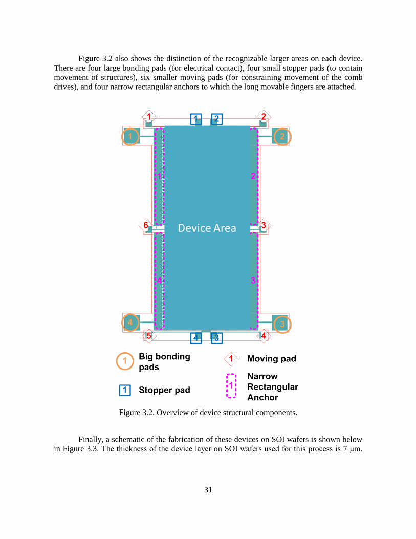
31
Figure 3.2 also shows the distinction of the recognizable larger areas on each device.
There are four large bonding pads (for electrical contact), four small stopper pads (to contain
movement of structures), six smaller moving pads (for constraining movement of the comb
drives), and four narrow rectangular anchors to which the long movable fingers are attached.
Device Area
Figure 3.2. Overview of device structural components.
Finally, a schematic of the fabrication of these devices on SOI wafers is shown below
in Figure 3.3. The thickness of the device layer on SOI wafers used for this process is 7 μm.
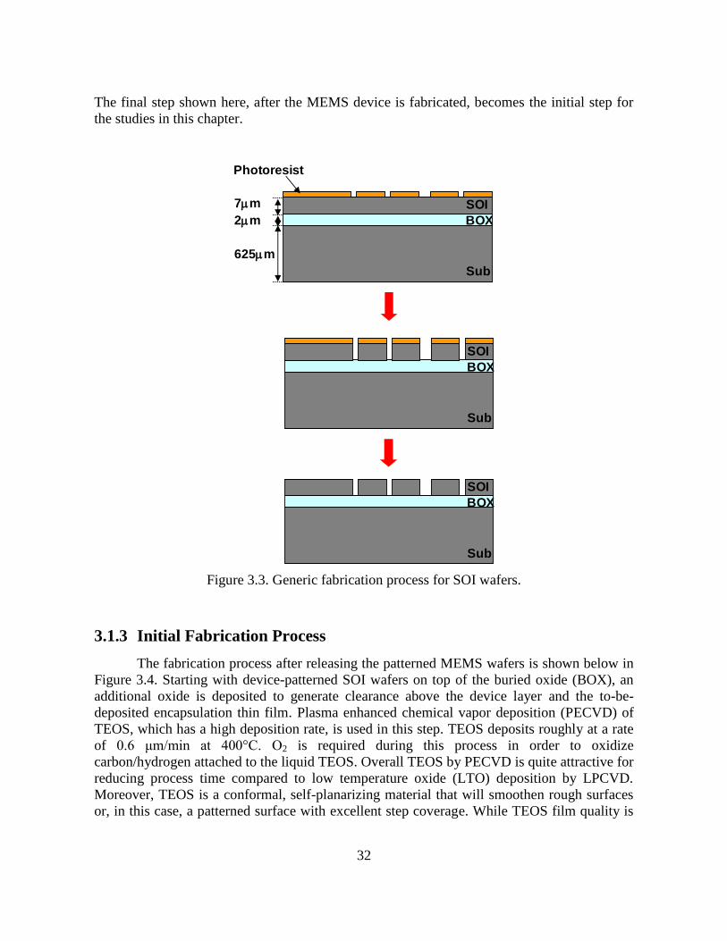
32
The final step shown here, after the MEMS device is fabricated, becomes the initial step for
the studies in this chapter.
Sub
BOX
SOI
625mm
2mm
7mm
Sub
BOX
SOI
Sub
BOX
SOI
Photoresist
Figure 3.3. Generic fabrication process for SOI wafers.
3.1.3 Initial Fabrication Process
The fabrication process after releasing the patterned MEMS wafers is shown below in
Figure 3.4. Starting with device-patterned SOI wafers on top of the buried oxide (BOX), an
additional oxide is deposited to generate clearance above the device layer and the to-be-
deposited encapsulation thin film. Plasma enhanced chemical vapor deposition (PECVD) of
TEOS, which has a high deposition rate, is used in this step. TEOS deposits roughly at a rate
of 0.6 μm/min at 400°C. O2 is required during this process in order to oxidize
carbon/hydrogen attached to the liquid TEOS. Overall TEOS by PECVD is quite attractive for
reducing process time compared to low temperature oxide (LTO) deposition by LPCVD.
Moreover, TEOS is a conformal, self-planarizing material that will smoothen rough surfaces
or, in this case, a patterned surface with excellent step coverage. While TEOS film quality is
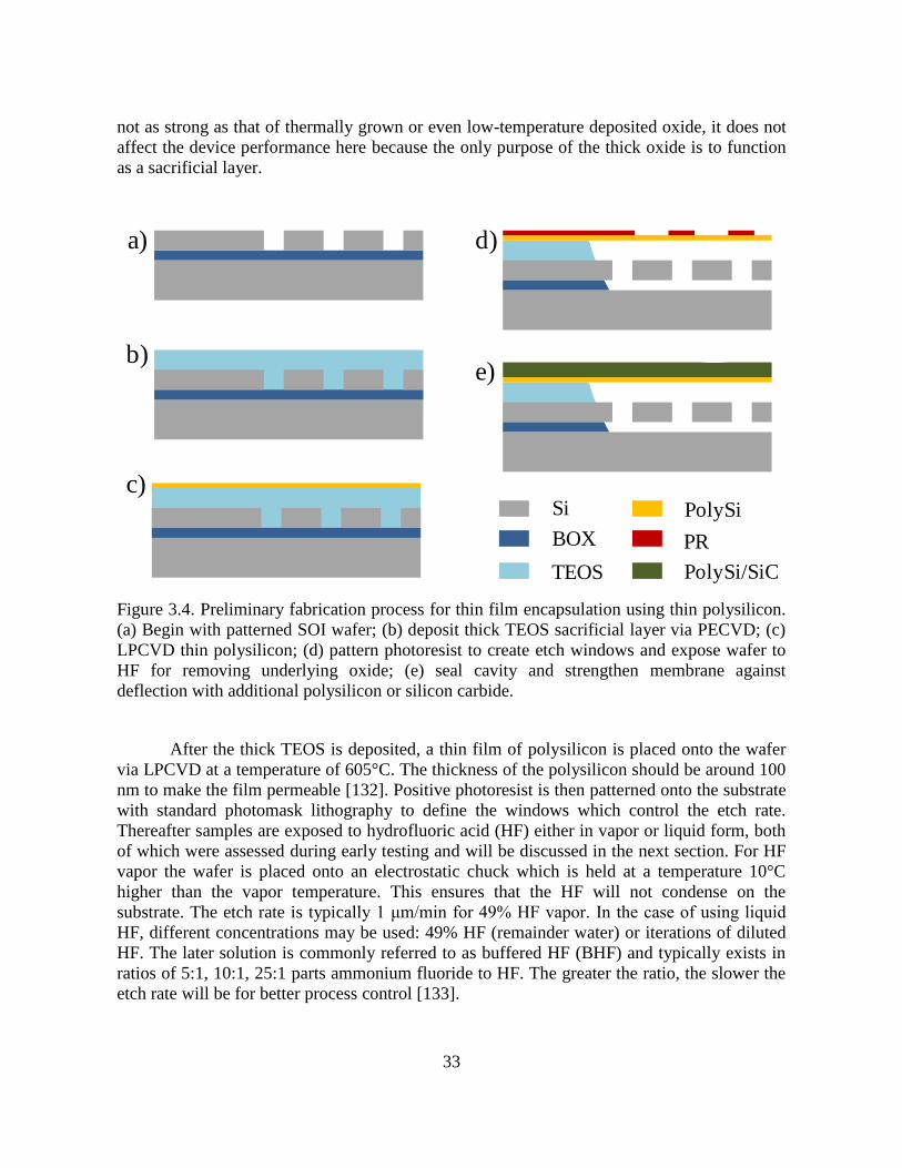
33
not as strong as that of thermally grown or even low-temperature deposited oxide, it does not
affect the device performance here because the only purpose of the thick oxide is to function
as a sacrificial layer.
a)
b)
c)
d)
Si
e)
BOX
TEOS
PolySi
PR
PolySi/SiC
Figure 3.4. Preliminary fabrication process for thin film encapsulation using thin polysilicon.
(a) Begin with patterned SOI wafer; (b) deposit thick TEOS sacrificial layer via PECVD; (c)
LPCVD thin polysilicon; (d) pattern photoresist to create etch windows and expose wafer to
HF for removing underlying oxide; (e) seal cavity and strengthen membrane against
deflection with additional polysilicon or silicon carbide.
After the thick TEOS is deposited, a thin film of polysilicon is placed onto the wafer
via LPCVD at a temperature of 605°C. The thickness of the polysilicon should be around 100
nm to make the film permeable [132]. Positive photoresist is then patterned onto the substrate
with standard photomask lithography to define the windows which control the etch rate.
Thereafter samples are exposed to hydrofluoric acid (HF) either in vapor or liquid form, both
of which were assessed during early testing and will be discussed in the next section. For HF
vapor the wafer is placed onto an electrostatic chuck which is held at a temperature 10°C
higher than the vapor temperature. This ensures that the HF will not condense on the
substrate. The etch rate is typically 1 μm/min for 49% HF vapor. In the case of using liquid
HF, different concentrations may be used: 49% HF (remainder water) or iterations of diluted
HF. The later solution is commonly referred to as buffered HF (BHF) and typically exists in
ratios of 5:1, 10:1, 25:1 parts ammonium fluoride to HF. The greater the ratio, the slower the
etch rate will be for better process control [133].
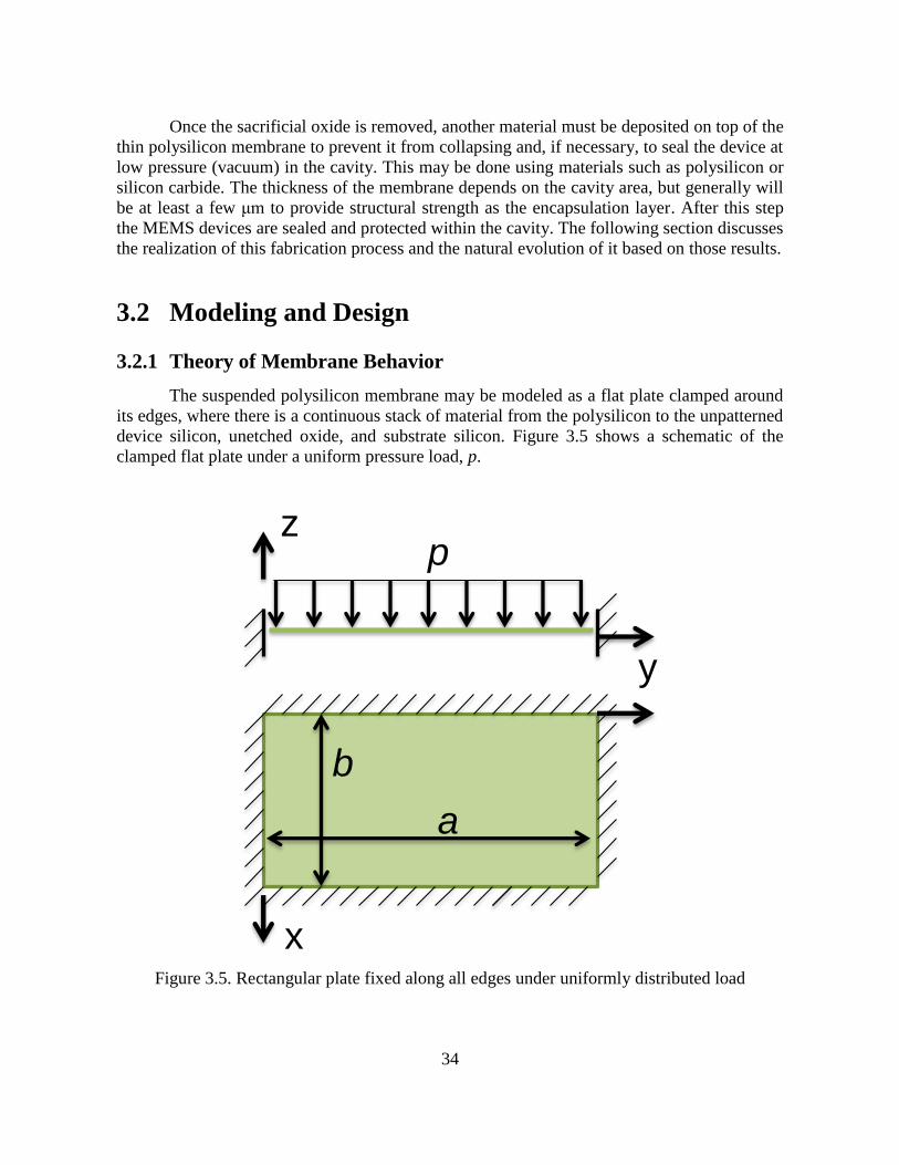
34
Once the sacrificial oxide is removed, another material must be deposited on top of the
thin polysilicon membrane to prevent it from collapsing and, if necessary, to seal the device at
low pressure (vacuum) in the cavity. This may be done using materials such as polysilicon or
silicon carbide. The thickness of the membrane depends on the cavity area, but generally will
be at least a few μm to provide structural strength as the encapsulation layer. After this step
the MEMS devices are sealed and protected within the cavity. The following section discusses
the realization of this fabrication process and the natural evolution of it based on those results.
3.2 Modeling and Design
3.2.1 Theory of Membrane Behavior
The suspended polysilicon membrane may be modeled as a flat plate clamped around
its edges, where there is a continuous stack of material from the polysilicon to the unpatterned
device silicon, unetched oxide, and substrate silicon. Figure 3.5 shows a schematic of the
clamped flat plate under a uniform pressure load, p.
y
x
z
b
a
p
Figure 3.5. Rectangular plate fixed along all edges under uniformly distributed load
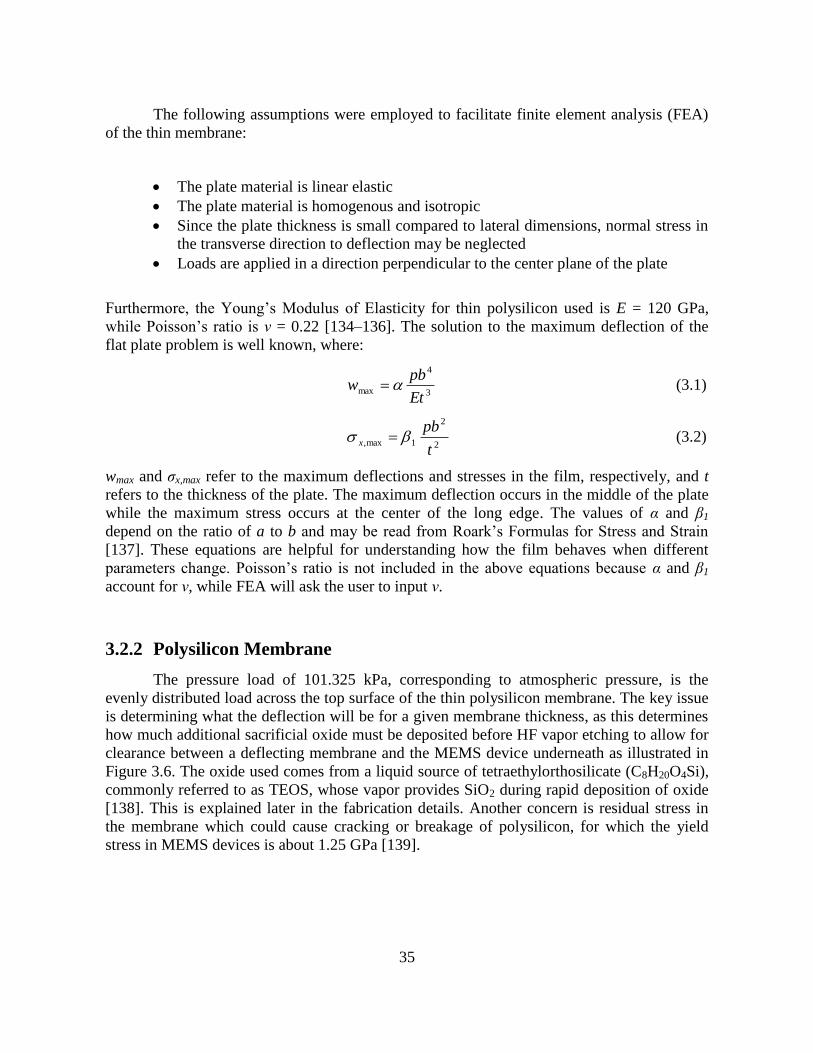
35
The following assumptions were employed to facilitate finite element analysis (FEA)
of the thin membrane:
The plate material is linear elastic
The plate material is homogenous and isotropic
Since the plate thickness is small compared to lateral dimensions, normal stress in
the transverse direction to deflection may be neglected
Loads are applied in a direction perpendicular to the center plane of the plate
Furthermore, the Young’s Modulus of Elasticity for thin polysilicon used is E = 120 GPa,
while Poisson’s ratio is ν = 0.22 [134–136]. The solution to the maximum deflection of the
flat plate problem is well known, where:
3
4
maxEt
pbw (3.1)
2
2
1max,t
pbx (3.2)
wmax and σx,max refer to the maximum deflections and stresses in the film, respectively, and t
refers to the thickness of the plate. The maximum deflection occurs in the middle of the plate
while the maximum stress occurs at the center of the long edge. The values of α and β1
depend on the ratio of a to b and may be read from Roark’s Formulas for Stress and Strain
[137]. These equations are helpful for understanding how the film behaves when different
parameters change. Poisson’s ratio is not included in the above equations because α and β1
account for ν, while FEA will ask the user to input ν.
3.2.2 Polysilicon Membrane
The pressure load of 101.325 kPa, corresponding to atmospheric pressure, is the
evenly distributed load across the top surface of the thin polysilicon membrane. The key issue
is determining what the deflection will be for a given membrane thickness, as this determines
how much additional sacrificial oxide must be deposited before HF vapor etching to allow for
clearance between a deflecting membrane and the MEMS device underneath as illustrated in
Figure 3.6. The oxide used comes from a liquid source of tetraethylorthosilicate (C8H20O4Si),
commonly referred to as TEOS, whose vapor provides SiO2 during rapid deposition of oxide
[138]. This is explained later in the fabrication details. Another concern is residual stress in
the membrane which could cause cracking or breakage of polysilicon, for which the yield
stress in MEMS devices is about 1.25 GPa [139].
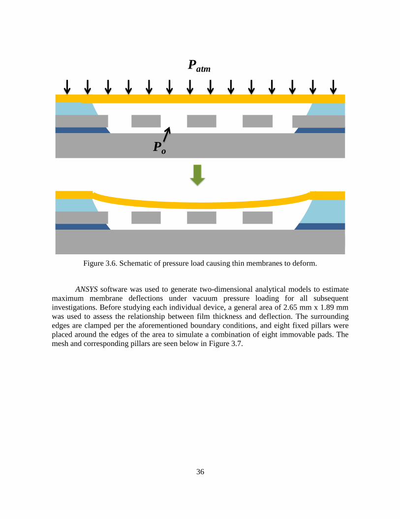
36
Patm
Po
Figure 3.6. Schematic of pressure load causing thin membranes to deform.
ANSYS software was used to generate two-dimensional analytical models to estimate
maximum membrane deflections under vacuum pressure loading for all subsequent
investigations. Before studying each individual device, a general area of 2.65 mm x 1.89 mm
was used to assess the relationship between film thickness and deflection. The surrounding
edges are clamped per the aforementioned boundary conditions, and eight fixed pillars were
placed around the edges of the area to simulate a combination of eight immovable pads. The
mesh and corresponding pillars are seen below in Figure 3.7.
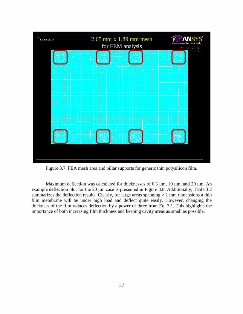
37
2.65 mm x 1.89 mm mesh
for FEM analysis
Figure 3.7. FEA mesh area and pillar supports for generic thin polysilicon film.
Maximum deflection was calculated for thicknesses of 0.3 μm, 10 μm, and 20 μm. An
example deflection plot for the 20 μm case is presented in Figure 3.8. Additionally, Table 3.2
summarizes the deflection results. Clearly, for large areas spanning > 1 mm dimensions a thin
film membrane will be under high load and deflect quite easily. However, changing the
thickness of the film reduces deflection by a power of three from Eq. 3.1. This highlights the
importance of both increasing film thickness and keeping cavity areas as small as possible.
38
plate thickness: 20μm
maximum deflection: 24.0μm
Figure 3.8. Two-dimensional plot of maximum deflection for a 20 μm thick polysilicon
membrane under vacuum load.
Table 3.2. Maximum deflection for differing polysilicon films spanning large area of 2.65 mm
x 1.89 mm.
Polysilicon
thickness
Maximum deflection
under vacuum load
0.3 μm 7.12 m
10 μm 192 μm
20 μm 24 μm
Following these results, 2D models representing the actual geometries for devices A,
B, C, and D seen in Figure 3.1 were generated using the full 2.9 mm x 2.9 mm area of each
die. The support for the membrane in each case comes from the four bonding pads used for
electrical contacts, detailed below in Figure 3.9, simulating a worst case scenario for large
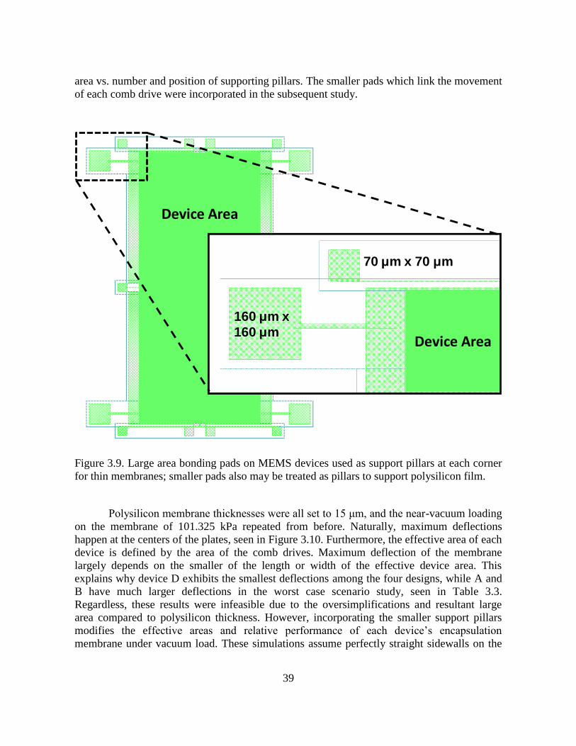
39
area vs. number and position of supporting pillars. The smaller pads which link the movement
of each comb drive were incorporated in the subsequent study.
160 μm x
160 μm
70 μm x 70 μm
Device Area
Device Area
Figure 3.9. Large area bonding pads on MEMS devices used as support pillars at each corner
for thin membranes; smaller pads also may be treated as pillars to support polysilicon film.
Polysilicon membrane thicknesses were all set to 15 μm, and the near-vacuum loading
on the membrane of 101.325 kPa repeated from before. Naturally, maximum deflections
happen at the centers of the plates, seen in Figure 3.10. Furthermore, the effective area of each
device is defined by the area of the comb drives. Maximum deflection of the membrane
largely depends on the smaller of the length or width of the effective device area. This
explains why device D exhibits the smallest deflections among the four designs, while A and
B have much larger deflections in the worst case scenario study, seen in Table 3.3.
Regardless, these results were infeasible due to the oversimplifications and resultant large
area compared to polysilicon thickness. However, incorporating the smaller support pillars
modifies the effective areas and relative performance of each device’s encapsulation
membrane under vacuum load. These simulations assume perfectly straight sidewalls on the

40
pillars and contact pads while the real structural shape should have curvatures due to the
etching and deposition processes.
Table 3.3. Maximum deflection for each device with 15 μm thick polysilicon membrane
Device Label Length Width Area Max. Deflection
A 1.54 mm 1.50 mm 2.3 mm2
168 μm
B 1.94 mm 1.50 mm 2.9 mm2 163 μm
C 2.34 mm 1.14 mm 2.7 mm2 113 μm
D 1.87 mm 1.14 mm 2.1 mm2 31 μm
Figure 3.10. 2D models in ANSYS for each membrane configuration based on support pad
positions, showing maximum deflection under vacuum load at the center of each film.
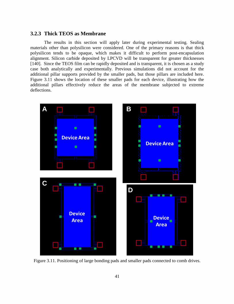
41
3.2.3 Thick TEOS as Membrane
The results in this section will apply later during experimental testing. Sealing
materials other than polysilicon were considered. One of the primary reasons is that thick
polysilicon tends to be opaque, which makes it difficult to perform post-encapsulation
alignment. Silicon carbide deposited by LPCVD will be transparent for greater thicknesses
[140]. Since the TEOS film can be rapidly deposited and is transparent, it is chosen as a study
case both analytically and experimentally. Previous simulations did not account for the
additional pillar supports provided by the smaller pads, but those pillars are included here.
Figure 3.11 shows the location of these smaller pads for each device, illustrating how the
additional pillars effectively reduce the areas of the membrane subjected to extreme
deflections.
Device Area
Device Area
Device AreaDevice Area
A B
CD
Figure 3.11. Positioning of large bonding pads and smaller pads connected to comb drives.

42
The ANSYS simulations were run with previous assumptions, simplifications, and
atmospheric pressure loading. Young’s Modulus for TEOS is 59 GPa, while Poisson’s ratio is
0.24 [141], [142].The thin polysilicon membrane was replaced with TEOS films of varying
thicknesses for simplicity during the simulations, but in reality the membrane is composed of
thin polysilicon on the bottom and thick TEOS on the top. As expected, the inclusion of the
smaller pillars reduced maximum membrane deflections by a significant portion for each
device design. Figure 3.12 demonstrates that a 15 μm TEOS film would keep film deflection
under 10 μm for two devices, A and D.
Figure 3.13 shows how the placement of the smaller pads altered the membrane
deflection behavior. This agrees with Figure 3.11 in that the smaller pads in A and D form the
narrowest enclosed areas. Overall, based on these results a 15 μm thick TEOS layer deposited
on top of polysilicon would sustain under vacuum loading with a membrane deformation of
10+ μm. Thick TEOS deposition is discussed later in Section 3.5.
Figure 3.12. Maximum film deflection vs. TEOS thickness for four different configurations.
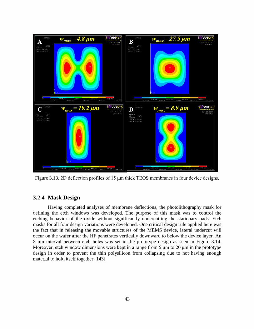
43
Figure 3.13. 2D deflection profiles of 15 μm thick TEOS membranes in four device designs.
3.2.4 Mask Design
Having completed analyses of membrane deflections, the photolithography mask for
defining the etch windows was developed. The purpose of this mask was to control the
etching behavior of the oxide without significantly undercutting the stationary pads. Etch
masks for all four design variations were developed. One critical design rule applied here was
the fact that in releasing the movable structures of the MEMS device, lateral undercut will
occur on the wafer after the HF penetrates vertically downward to below the device layer. An
8 μm interval between etch holes was set in the prototype design as seen in Figure 3.14.
Moreover, etch window dimensions were kept in a range from 5 μm to 20 μm in the prototype
design in order to prevent the thin polysilicon from collapsing due to not having enough
material to hold itself together [143].
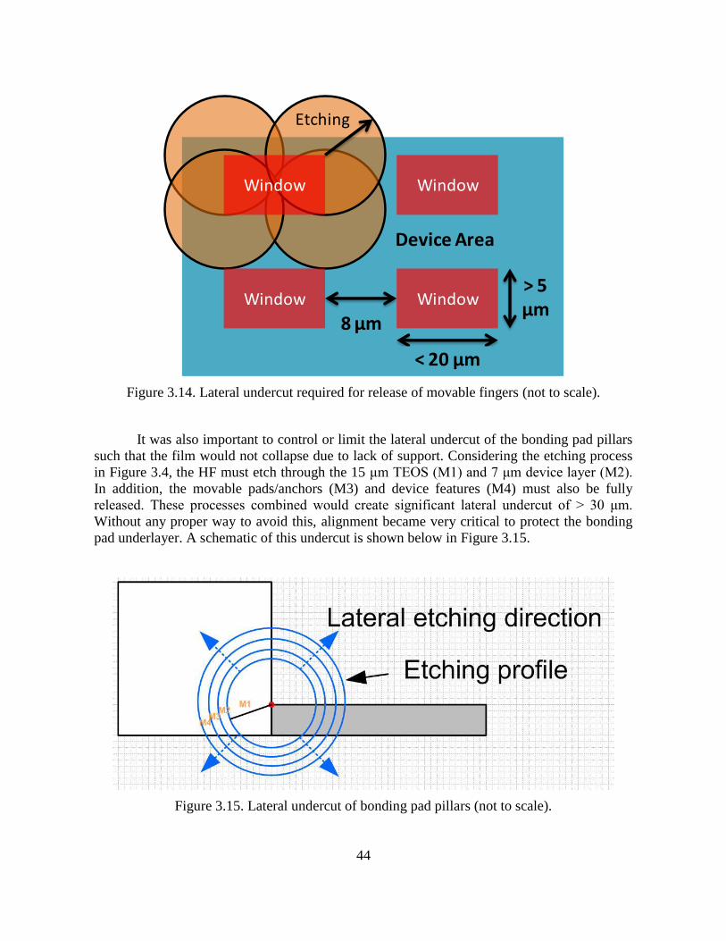
44
Device Area
Window Window
WindowWindow
8 μm
Etching
< 20 μm
> 5 μm
Figure 3.14. Lateral undercut required for release of movable fingers (not to scale).
It was also important to control or limit the lateral undercut of the bonding pad pillars
such that the film would not collapse due to lack of support. Considering the etching process
in Figure 3.4, the HF must etch through the 15 μm TEOS (M1) and 7 μm device layer (M2).
In addition, the movable pads/anchors (M3) and device features (M4) must also be fully
released. These processes combined would create significant lateral undercut of > 30 μm.
Without any proper way to avoid this, alignment became very critical to protect the bonding
pad underlayer. A schematic of this undercut is shown below in Figure 3.15.
Figure 3.15. Lateral undercut of bonding pad pillars (not to scale).

45
Due to uncertainty about the HF etching behavior, two mask designs were created for
each device: “conservative” and “original”. The conservative design limits etch holes to the
area confined by the smaller pillars while the original design allows for HF penetration
throughout the entire device layout. The distinction between these two is shown below in
Figure 3.16 for design D.
SOI layer for referenceOriginalConservative
Figure 3.16. Comparison of “conservative” and “original” etch mask layouts.
3.3 Assessing Permeability of Polysilicon
3.3.1 Preliminary Studies
In order to test the permeability of polysilicon, bare silicon wafers with 1.4 μm of low
temperature oxide were used. Approximately 0.1 μm of polysilicon was deposited onto the
wafers, and positive photoresist was used to define etch windows on the substrates using the
mask design previously discussed. Thereafter individual chips were either dipped into 49%
HF solution or exposed to HF vapor for different lengths of time. BHF was not used since the
etch rate would be slower, plus it has been reported that 5:1 BHF will attack polysilicon
[144]. After the HF step photoresist was stripped and tetramethyl ammonium hydroxide
(TMAH) was used to etch away the polysilicon and inspect the oxide profile as TMAH would
not etch oxide [145]. The results of these experiments are summarized below in Table 3.4.
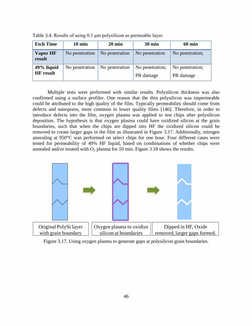
46
Table 3.4. Results of using 0.1 μm polysilicon as permeable layer.
Etch Time 10 min 20 min 30 min 60 min
Vapor HF
result
No penetration No penetration No penetration No penetration;
49% liquid
HF result
No penetration No penetration No penetration;
PR damage
No penetration;
PR damage
Multiple tests were performed with similar results. Polysilicon thickness was also
confirmed using a surface profiler. One reason that the thin polysilicon was impermeable
could be attributed to the high quality of the film. Typically permeability should come from
defects and nanopores, more common in lower quality films [146]. Therefore, in order to
introduce defects into the film, oxygen plasma was applied to test chips after polysilicon
deposition. The hypothesis is that oxygen plasma could have oxidized silicon at the grain
boundaries, such that when the chips are dipped into HF the oxidized silicon could be
removed to create larger gaps in the film as illustrated in Figure 3.17. Additionally, nitrogen
annealing at 950°C was performed on select chips for one hour. Four different cases were
tested for permeability of 49% HF liquid, based on combinations of whether chips were
annealed and/or treated with O2 plasma for 10 min. Figure 3.18 shows the results.
Original PolySi layer
with grain boundary
Oxygen plasma to oxidize
silicon at boundaries
Dipped in HF, Oxide
removed, larger gaps formed.
Figure 3.17. Using oxygen plasma to generate gaps at polysilicon grain boundaries.

47
No O2
plasma
treatment
O2 plasma
treatment
Polysilicon
annealed
Polysilicon
unannealed
Figure 3.18. Results of annealing and oxygen plasma treatment of polysilicon films.
For the unannealed chips, it is found that thin polysilicon films crack due to residual
stress without an annealing process. For the annealed chips it is found that HF is not able to
penetrate the polysilicon film. At this point, amorphous silicon was considered an alternative
to polysilicon as the thin film membrane. Amorphous silicon (a-Si) may be deposited by
PECVD at temperatures as low as 75°C [147]. Deposition temperatures from 75°C to 350°C
were used to deposit 0.1 μm of a-Si. It was found that lower deposition temperatures yielded
better permeability for 49% liquid HF but the film was extremely fragile and broke when the
underlying oxide was removed. Higher deposition temperatures yielded better quality films
that were impenetrable.
Therefore, it was decided that polysilicon should be doped to induce defects in the
film. During a high temperature anneal dopant atoms segregate and create tiny gaps for HF
(or another liquid/vapor) to penetrate. The dopants could come from both in-situ polysilicon
deposition as well as a drive-in process from the phosphosilicate glass (PSG). For example,
annealing the thin polysilicon film on top of the PSG drives the dopant into the polysilicon,
and the PSG must also be densified immediately after that deposition [143]. The test process
was as follows:
PSG deposition via LPCVD, 450°C, 1.5 hours, 300 mTorr, 105 sccm SiH4, 150
sccm O2, 15 sccm PH3

48
PSG densification, 950°C, 1 hour,
Polysilicon deposition via LPCVD, 605°C, 15 min, 555 mTorr, 125 sccm SiH4
Annealing/dopant drive-in, 950°C, 1 hour
Manually paint photoresist onto chip to create small open area
Subjecting patterned chips to 49% HF liquid resulted in successful penetration through
polysilicon and removal of the oxide underneath. However, one drawback was that the liquid
surface tension from HF caused the thin film to crash onto the substrate. Figure 3.19 shows an
image captured with a microscope of the etch window and oxide removal, facilitated by the
transparency of thin polysilicon.
Thus, permeable polysilicon was generated using the doping approach with a PSG
underlayer. With this in mind the fabrication process in Sec. 3.1.3 calls for additional steps.
The thick TEOS sacrificial layer may still be used, but PSG should be deposited on top of it to
interact with the polysilicon during annealing and provide dopant diffusion. Replacing TEOS
generates an issue with requiring to planarize a very thick PSG layer with chemical
mechanical polishing (CMP), an often inconsistent operation. TEOS is also preferred due to
the rapid deposition rate.
5x mag
Etch
window
Oxide
removed
Figure 3.19. Successful penetration of doped polysilion and oxide etching.
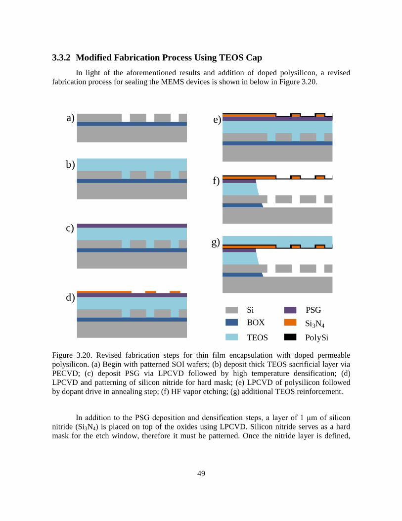
49
3.3.2 Modified Fabrication Process Using TEOS Cap
In light of the aforementioned results and addition of doped polysilicon, a revised
fabrication process for sealing the MEMS devices is shown in below in Figure 3.20.
a)
b)
c)
d)
e)
f)
g)
Si
BOX
TEOS
PSG
Si3N4
PolySi
Figure 3.20. Revised fabrication steps for thin film encapsulation with doped permeable
polysilicon. (a) Begin with patterned SOI wafers; (b) deposit thick TEOS sacrificial layer via
PECVD; (c) deposit PSG via LPCVD followed by high temperature densification; (d)
LPCVD and patterning of silicon nitride for hard mask; (e) LPCVD of polysilicon followed
by dopant drive in annealing step; (f) HF vapor etching; (g) additional TEOS reinforcement.
In addition to the PSG deposition and densification steps, a layer of 1 μm of silicon
nitride (Si3N4) is placed on top of the oxides using LPCVD. Silicon nitride serves as a hard
mask for the etch window, therefore it must be patterned. Once the nitride layer is defined,
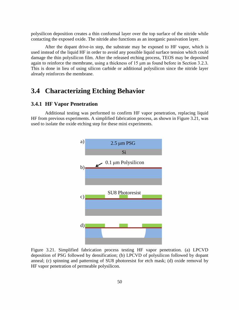
50
polysilicon deposition creates a thin conformal layer over the top surface of the nitride while
contacting the exposed oxide. The nitride also functions as an inorganic passivation layer.
After the dopant drive-in step, the substrate may be exposed to HF vapor, which is
used instead of the liquid HF in order to avoid any possible liquid surface tension which could
damage the thin polysilicon film. After the released etching process, TEOS may be deposited
again to reinforce the membrane, using a thickness of 15 μm as found before in Section 3.2.3.
This is done in lieu of using silicon carbide or additional polysilicon since the nitride layer
already reinforces the membrane.
3.4 Characterizing Etching Behavior
3.4.1 HF Vapor Penetration
Additional testing was performed to confirm HF vapor penetration, replacing liquid
HF from previous experiments. A simplified fabrication process, as shown in Figure 3.21, was
used to isolate the oxide etching step for these mini experiments.
Si
2.5 μm PSG
0.1 μm Polysilicon
a)
b)
c)
d)
SU8 Photoresist
Figure 3.21. Simplified fabrication process testing HF vapor penetration. (a) LPCVD
deposition of PSG followed by densification; (b) LPCVD of polysilicon followed by dopant
anneal; (c) spinning and patterning of SU8 photoresist for etch mask; (d) oxide removal by
HF vapor penetration of permeable polysilicon.
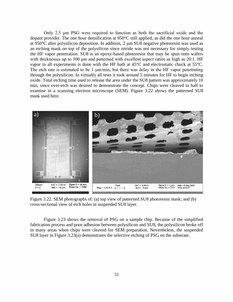
51
Only 2.5 μm PSG were required to function as both the sacrificial oxide and the
dopant provider. The one hour densification at 950°C still applied, as did the one hour anneal
at 950°C after polysilicon deposition. In addition, 2 μm SU8 negative photoresist was used as
an etching mask on top of the polysilicon since nitride was not necessary for simply testing
the HF vapor penetration. SU8 is an epoxy-based photoresist that may be spun onto wafers
with thicknesses up to 300 μm and patterned with excellent aspect ratios as high as 20:1. HF
vapor in all experiments is done with the HF bath at 45°C and electrostatic chuck at 55°C.
The etch rate is estimated to be 1 μm/min, but there was delay in the HF vapor penetrating
through the polysilicon. In virtually all tests it took around 5 minutes for HF to begin etching
oxide. Total etching time used to release the area under the SU8 pattern was approximately 10
min, since over-etch was desired to demonstrate the concept. Chips were cleaved in half to
examine in a scanning electron microscope (SEM). Figure 3.22 shows the patterned SU8
mask used here.
a) b)
Figure 3.22. SEM photographs of: (a) top view of patterned SU8 photoresist mask; and (b)
cross-sectional view of etch holes in suspended SU8 layer.
Figure 3.23 shows the removal of PSG on a sample chip. Because of the simplified
fabrication process and poor adhesion between polysilicon and SU8, the polysilicon broke off
in many areas when chips were cleaved for SEM preparation. Nevertheless, the suspended
SU8 layer in Figure 3.23(a) demonstrates the selective etching of PSG on the substrate.
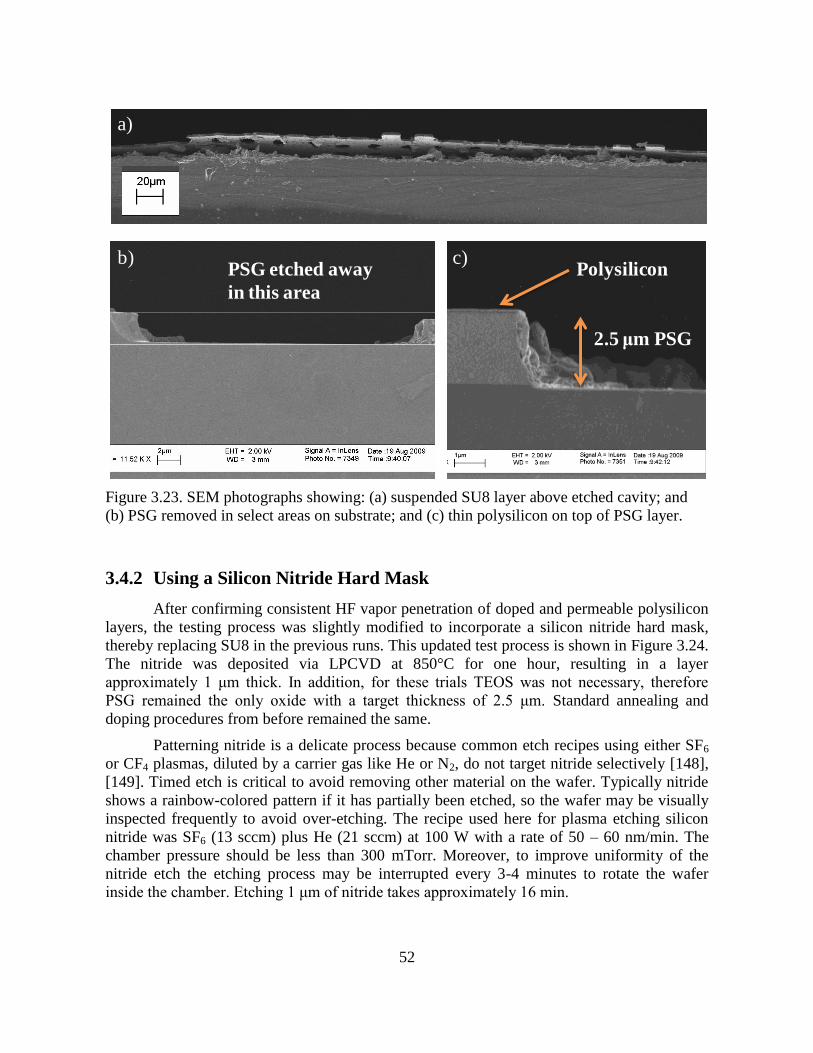
52
Polysilicon
2.5 μm PSG
PSG etched away
in this area
b) c)
a)
Figure 3.23. SEM photographs showing: (a) suspended SU8 layer above etched cavity; and
(b) PSG removed in select areas on substrate; and (c) thin polysilicon on top of PSG layer.
3.4.2 Using a Silicon Nitride Hard Mask
After confirming consistent HF vapor penetration of doped and permeable polysilicon
layers, the testing process was slightly modified to incorporate a silicon nitride hard mask,
thereby replacing SU8 in the previous runs. This updated test process is shown in Figure 3.24.
The nitride was deposited via LPCVD at 850°C for one hour, resulting in a layer
approximately 1 μm thick. In addition, for these trials TEOS was not necessary, therefore
PSG remained the only oxide with a target thickness of 2.5 μm. Standard annealing and
doping procedures from before remained the same.
Patterning nitride is a delicate process because common etch recipes using either SF6
or CF4 plasmas, diluted by a carrier gas like He or N2, do not target nitride selectively [148],
[149]. Timed etch is critical to avoid removing other material on the wafer. Typically nitride
shows a rainbow-colored pattern if it has partially been etched, so the wafer may be visually
inspected frequently to avoid over-etching. The recipe used here for plasma etching silicon
nitride was SF6 (13 sccm) plus He (21 sccm) at 100 W with a rate of 50 – 60 nm/min. The
chamber pressure should be less than 300 mTorr. Moreover, to improve uniformity of the
nitride etch the etching process may be interrupted every 3-4 minutes to rotate the wafer
inside the chamber. Etching 1 μm of nitride takes approximately 16 min.
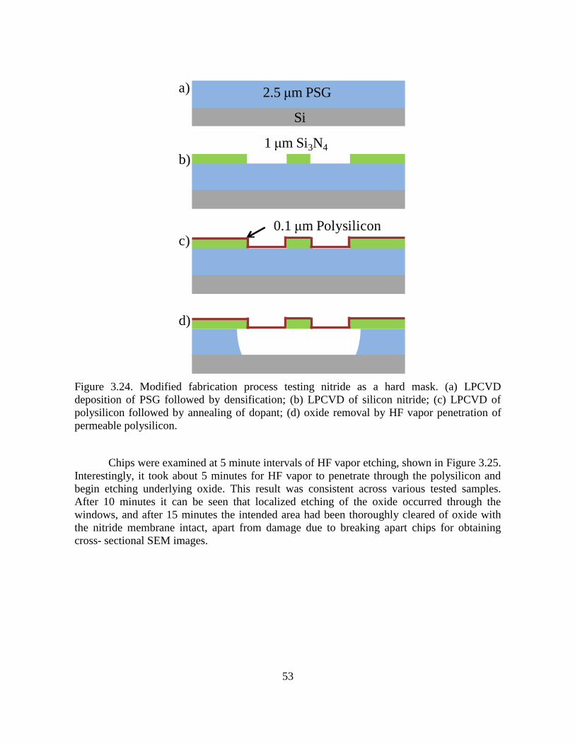
53
Si
2.5 μm PSG
0.1 μm Polysilicon
a)
b)
c)
d)
1 μm Si3N4
Figure 3.24. Modified fabrication process testing nitride as a hard mask. (a) LPCVD
deposition of PSG followed by densification; (b) LPCVD of silicon nitride; (c) LPCVD of
polysilicon followed by annealing of dopant; (d) oxide removal by HF vapor penetration of
permeable polysilicon.
Chips were examined at 5 minute intervals of HF vapor etching, shown in Figure 3.25.
Interestingly, it took about 5 minutes for HF vapor to penetrate through the polysilicon and
begin etching underlying oxide. This result was consistent across various tested samples.
After 10 minutes it can be seen that localized etching of the oxide occurred through the
windows, and after 15 minutes the intended area had been thoroughly cleared of oxide with
the nitride membrane intact, apart from damage due to breaking apart chips for obtaining
cross- sectional SEM images.
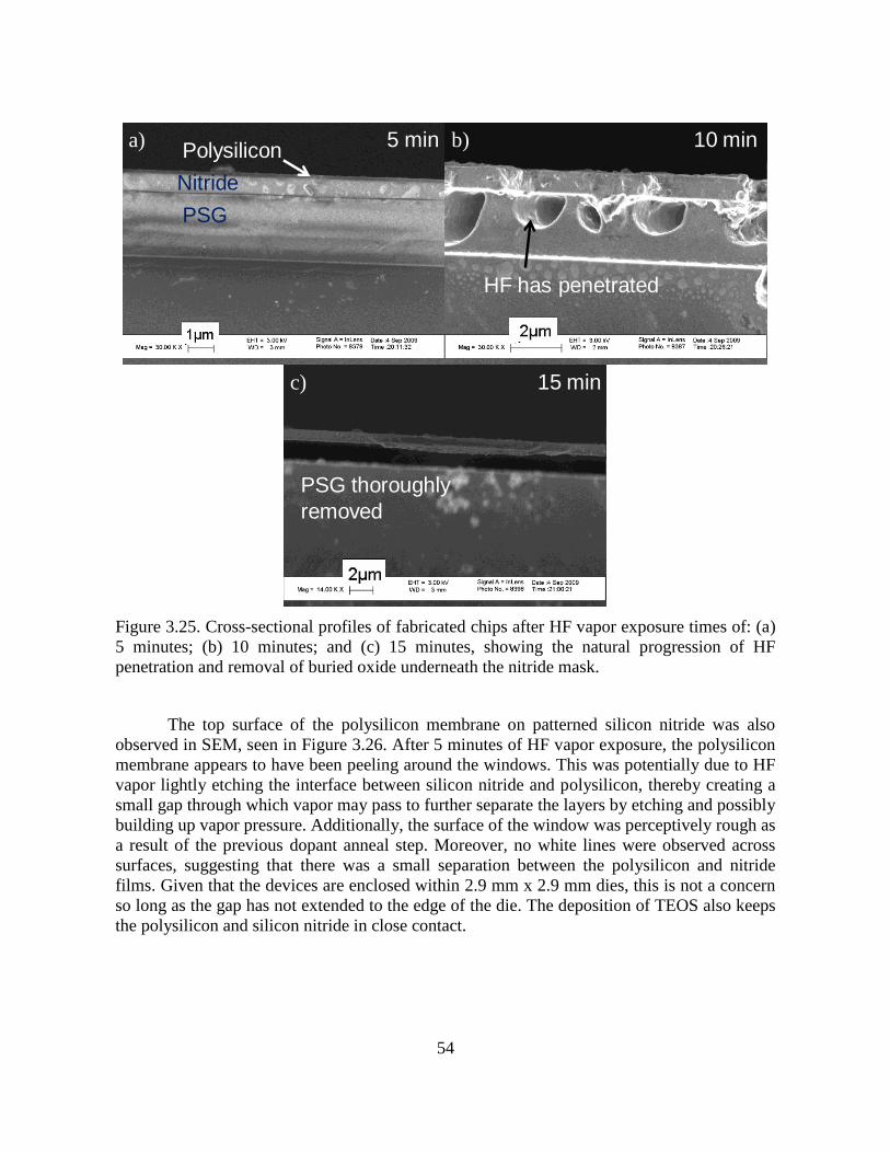
54
10
min
utes
HF penetration
occurs after ~5
minutes
10 min
HF has penetrated
5 min
Nitride
PSG
Polysilicon
10
minu
tes
Windows in nitride
film not clearly visible
due to breaking apart
devices
15 min
PSG thoroughly
removed
a) b)
c)
Figure 3.25. Cross-sectional profiles of fabricated chips after HF vapor exposure times of: (a)
5 minutes; (b) 10 minutes; and (c) 15 minutes, showing the natural progression of HF
penetration and removal of buried oxide underneath the nitride mask.
The top surface of the polysilicon membrane on patterned silicon nitride was also
observed in SEM, seen in Figure 3.26. After 5 minutes of HF vapor exposure, the polysilicon
membrane appears to have been peeling around the windows. This was potentially due to HF
vapor lightly etching the interface between silicon nitride and polysilicon, thereby creating a
small gap through which vapor may pass to further separate the layers by etching and possibly
building up vapor pressure. Additionally, the surface of the window was perceptively rough as
a result of the previous dopant anneal step. Moreover, no white lines were observed across
surfaces, suggesting that there was a small separation between the polysilicon and nitride
films. Given that the devices are enclosed within 2.9 mm x 2.9 mm dies, this is not a concern
so long as the gap has not extended to the edge of the die. The deposition of TEOS also keeps
the polysilicon and silicon nitride in close contact.
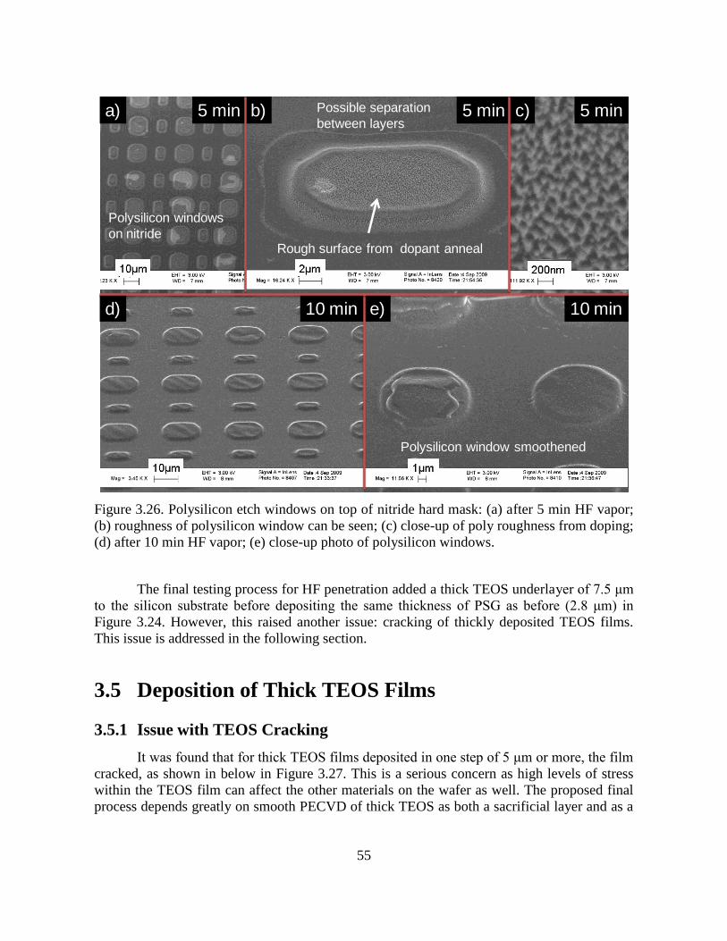
55
5 min
Polysilicon windows
on nitride
Possible separation
between layers
Rough surface from dopant anneal
5 min5 min
10 min 10 min
a) b) c)
d) e)
Polysilicon window smoothened
Figure 3.26. Polysilicon etch windows on top of nitride hard mask: (a) after 5 min HF vapor;
(b) roughness of polysilicon window can be seen; (c) close-up of poly roughness from doping;
(d) after 10 min HF vapor; (e) close-up photo of polysilicon windows.
The final testing process for HF penetration added a thick TEOS underlayer of 7.5 μm
to the silicon substrate before depositing the same thickness of PSG as before (2.8 μm) in
Figure 3.24. However, this raised another issue: cracking of thickly deposited TEOS films.
This issue is addressed in the following section.
3.5 Deposition of Thick TEOS Films
3.5.1 Issue with TEOS Cracking
It was found that for thick TEOS films deposited in one step of 5 μm or more, the film
cracked, as shown in below in Figure 3.27. This is a serious concern as high levels of stress
within the TEOS film can affect the other materials on the wafer as well. The proposed final
process depends greatly on smooth PECVD of thick TEOS as both a sacrificial layer and as a
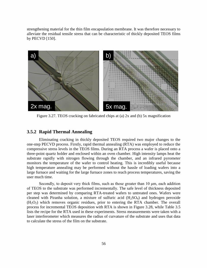
56
strengthening material for the thin film encapsulation membrane. It was therefore necessary to
alleviate the residual tensile stress that can be characteristic of thickly deposited TEOS films
by PECVD [150].
a) b)
2x mag. 5x mag.
Figure 3.27. TEOS cracking on fabricated chips at (a) 2x and (b) 5x magnification
3.5.2 Rapid Thermal Annealing
Eliminating cracking in thickly deposited TEOS required two major changes to the
one-step PECVD process. Firstly, rapid thermal annealing (RTA) was employed to reduce the
compressive stress levels in the TEOS films. During an RTA process a wafer is placed onto a
three-point quartz holder and enclosed within an oven chamber. High intensity lamps heat the
substrate rapidly with nitrogen flowing through the chamber, and an infrared pyrometer
monitors the temperature of the wafer to control heating. This is incredibly useful because
high temperature annealing may be performed without the hassle of loading wafers into a
large furnace and waiting for the large furnace zones to reach process temperatures, saving the
user much time.
Secondly, to deposit very thick films, such as those greater than 10 μm, each addition
of TEOS to the substrate was performed incrementally. The safe level of thickness deposited
per step was determined by comparing RTA-treated wafers to untreated ones. Wafers were
cleaned with Piranha solution, a mixture of sulfuric acid (H2SO4) and hydrogen peroxide
(H2O2) which removes organic residues, prior to entering the RTA chamber. The overall
process for incremental TEOS deposition with RTA is shown in Figure 3.28, while Table 3.5
lists the recipe for the RTA used in these experiments. Stress measurements were taken with a
laser interferometer which measures the radius of curvature of the substrate and uses that data
to calculate the stress of the film on the substrate.

57
1st TEOS
2nd TEOS
Si
Rapid Thermal Annealing
Measure stress in film
Repeat
a)
b)
c)
d)
Figure 3.28. Thick TEOS deposition with rapid thermal annealing: (a) deposit 1st TEOS layer
via PECVD; (b) clean wafer and perform RTA; (c) measure stress in deposited film with laser
interferometer; (d) repeat until desired TEOS thickness is reached
Table 3.5. Rapid thermal anneal process for TEOS films.
Step Description Time
0 Standby at 200°C --
1 Ramp to 450°C 10 sec
2 Hold at 450°C 30 sec
3 Ramp to 900°C 15 sec
4 Hold at 900°C 120 sec
5 Cool down with N2 purge 180 sec
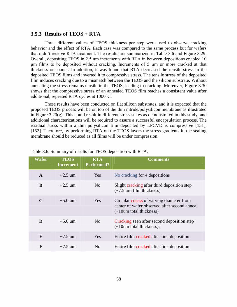
58
3.5.3 Results of TEOS + RTA
Three different values of TEOS thickness per step were used to observe cracking
behavior and the effect of RTA. Each case was compared to the same process but for wafers
that didn’t receive RTA treatment. The results are summarized in Table 3.6 and Figure 3.29.
Overall, depositing TEOS in 2.5 μm increments with RTA in between depositions enabled 10
μm films to be deposited without cracking. Increments of 5 μm or more cracked at that
thickness or sooner. In addition, it was found that RTA decreased the tensile stress in the
deposited TEOS films and inverted it to compressive stress. The tensile stress of the deposited
film induces cracking due to a mismatch between the TEOS and the silicon substrate. Without
annealing the stress remains tensile in the TEOS, leading to cracking. Moreover, Figure 3.30
shows that the compressive stress of an annealed TEOS film reaches a consistent value after
additional, repeated RTA cycles at 1000°C.
These results have been conducted on flat silicon substrates, and it is expected that the
proposed TEOS process will be on top of the thin nitride/polysilicon membrane as illustrated
in Figure 3.20(g). This could result in different stress states as demonstrated in this study, and
additional characterizations will be required to assure a successful encapsulation process. The
residual stress within a thin polysilicon film deposited by LPCVD is compressive [151],
[152]. Therefore, by performing RTA on the TEOS layers the stress gradients in the sealing
membrane should be reduced as all films will be under compression.
Table 3.6. Summary of results for TEOS deposition with RTA.
Wafer TEOS
Increment
RTA
Performed?
Comments
A ~2.5 um Yes No cracking for 4 depositions
B ~2.5 um No Slight cracking after third deposition step
(~7.5 μm film thickness)
C ~5.0 um Yes Circular cracks of varying diameter from
center of wafer observed after second anneal
(~10um total thickness)
D ~5.0 um No Cracking seen after second deposition step
(~10um total thickness);
E ~7.5 um Yes Entire film cracked after first deposition
F ~7.5 um No Entire film cracked after first deposition
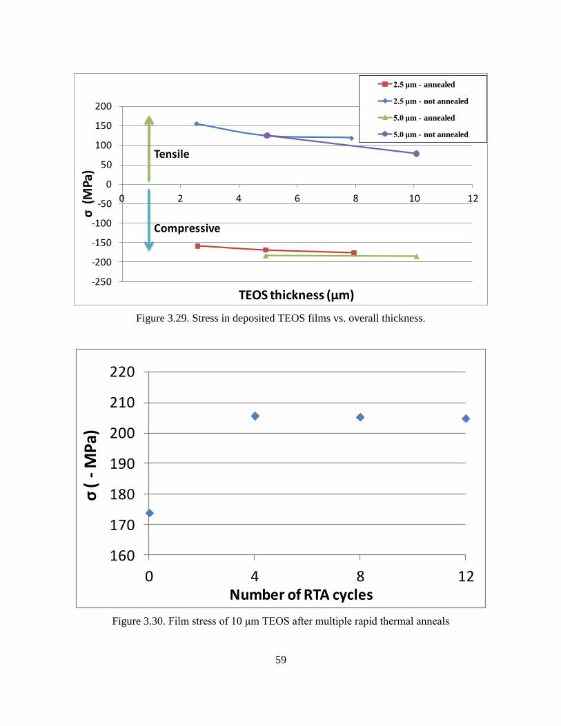
59
-250
-200
-150
-100
-50
0
50
100
150
200
0 2 4 6 8 10 12
σ(M
Pa)
TEOS thickness (μm)
2.5 μm - annealed
2.5 μm - not annealed
5.0 μm - annealed
5.0 μm - not annealed
Tensile
Compressive
Figure 3.29. Stress in deposited TEOS films vs. overall thickness.
160
170
180
190
200
210
220
0 4 8 12
σ(
-M
Pa)
Number of RTA cycles
Figure 3.30. Film stress of 10 μm TEOS after multiple rapid thermal anneals
60
3.6 Summary
In this chapter the potential for encapsulating MEMS devices with thin films was
investigated using permeable polysilicon membranes. A process involving high temperature
annealing to drive dopant atoms in thin polysilicon films has been developed to make
permeable polysilicon films. 2D modeling of plate deflection guided the design of the sealing
membrane, which incorporates a supporting layer of silicon nitride, functioning as a hard
mask, and additional sealing such as TEOS oxide for structural support in the form of
increased thickness. It was found that HF vapor may penetrate the permeable polysilicon thin
film in just a few minutes to etch buried oxide underneath the film.
While cracking occurs in thickly deposited TEOS films due to residual tensile
strength, an effective deposition process to avoid this was developed. Incremental depositions
of 2.5 μm TEOS followed by rapid thermal annealing alleviated stress in the film and even
made it compressive such that cracking did not occur. Films greater than 10 μm thick may be
generated using this approach, saving much fabrication time compared to oxide deposition by
low pressure chemical vapor deposition. This is beneficial for both building up the sacrificial
oxide layer and the sealing layer. Therefore, the combination of permeable polysilicon and
TEOS could provide an effective framework for MEMS packaging applications.
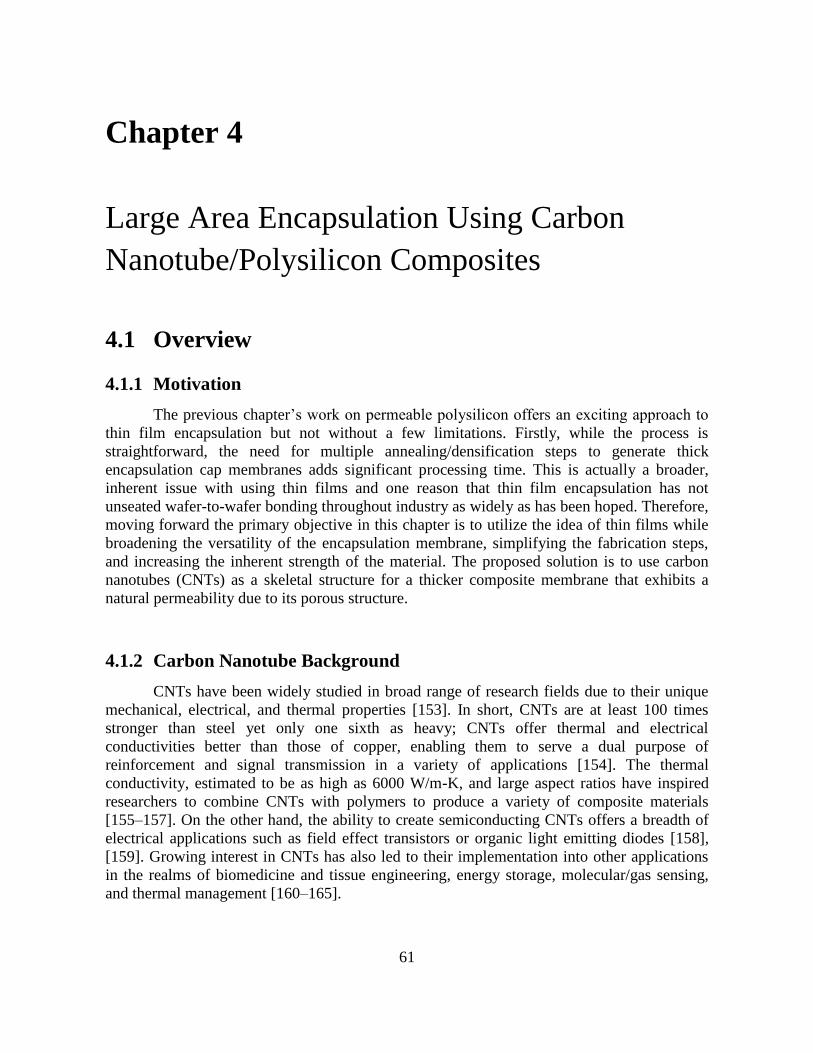
61
Chapter 4
Large Area Encapsulation Using Carbon
Nanotube/Polysilicon Composites
4.1 Overview
4.1.1 Motivation
The previous chapter’s work on permeable polysilicon offers an exciting approach to
thin film encapsulation but not without a few limitations. Firstly, while the process is
straightforward, the need for multiple annealing/densification steps to generate thick
encapsulation cap membranes adds significant processing time. This is actually a broader,
inherent issue with using thin films and one reason that thin film encapsulation has not
unseated wafer-to-wafer bonding throughout industry as widely as has been hoped. Therefore,
moving forward the primary objective in this chapter is to utilize the idea of thin films while
broadening the versatility of the encapsulation membrane, simplifying the fabrication steps,
and increasing the inherent strength of the material. The proposed solution is to use carbon
nanotubes (CNTs) as a skeletal structure for a thicker composite membrane that exhibits a
natural permeability due to its porous structure.
4.1.2 Carbon Nanotube Background
CNTs have been widely studied in broad range of research fields due to their unique
mechanical, electrical, and thermal properties [153]. In short, CNTs are at least 100 times
stronger than steel yet only one sixth as heavy; CNTs offer thermal and electrical
conductivities better than those of copper, enabling them to serve a dual purpose of
reinforcement and signal transmission in a variety of applications [154]. The thermal
conductivity, estimated to be as high as 6000 W/m-K, and large aspect ratios have inspired
researchers to combine CNTs with polymers to produce a variety of composite materials
[155–157]. On the other hand, the ability to create semiconducting CNTs offers a breadth of
electrical applications such as field effect transistors or organic light emitting diodes [158],
[159]. Growing interest in CNTs has also led to their implementation into other applications
in the realms of biomedicine and tissue engineering, energy storage, molecular/gas sensing,
and thermal management [160–165].
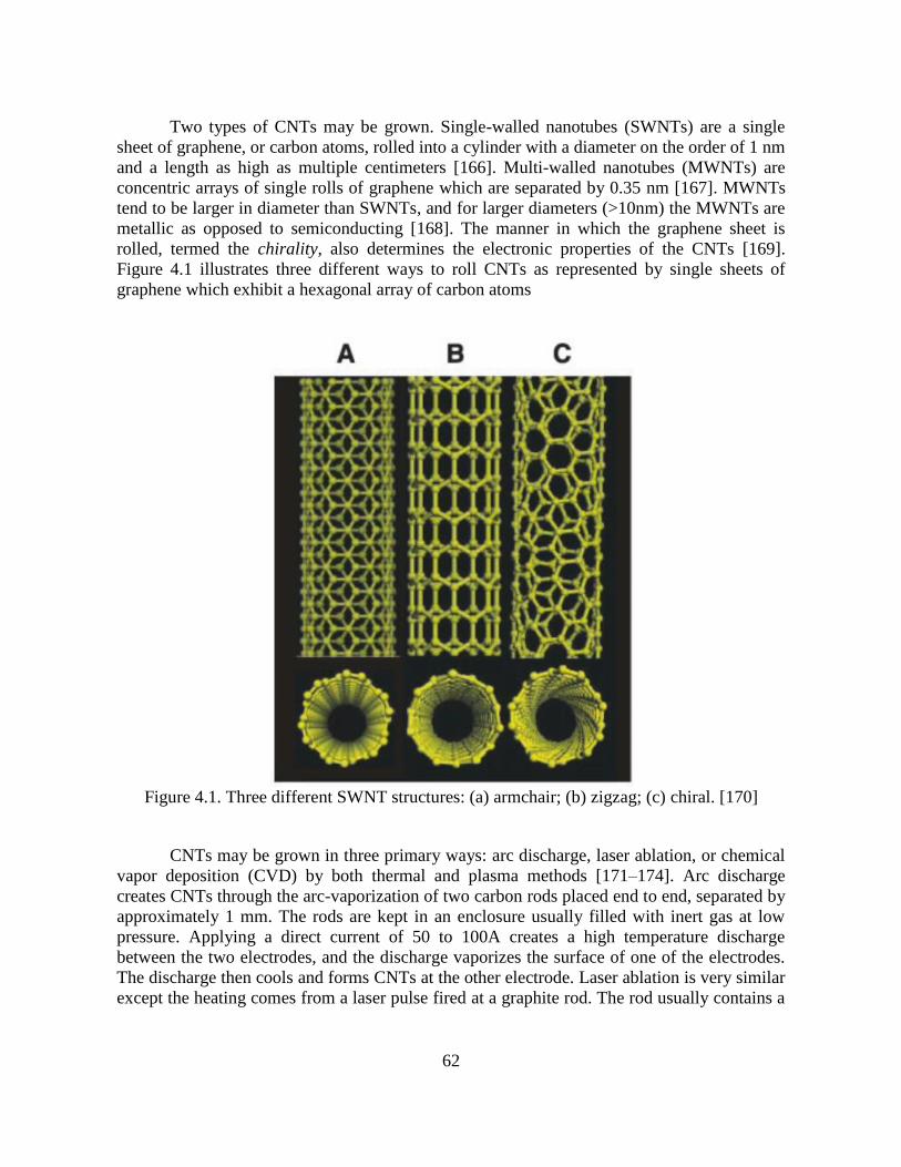
62
Two types of CNTs may be grown. Single-walled nanotubes (SWNTs) are a single
sheet of graphene, or carbon atoms, rolled into a cylinder with a diameter on the order of 1 nm
and a length as high as multiple centimeters [166]. Multi-walled nanotubes (MWNTs) are
concentric arrays of single rolls of graphene which are separated by 0.35 nm [167]. MWNTs
tend to be larger in diameter than SWNTs, and for larger diameters (>10nm) the MWNTs are
metallic as opposed to semiconducting [168]. The manner in which the graphene sheet is
rolled, termed the chirality, also determines the electronic properties of the CNTs [169].
Figure 4.1 illustrates three different ways to roll CNTs as represented by single sheets of
graphene which exhibit a hexagonal array of carbon atoms
Figure 4.1. Three different SWNT structures: (a) armchair; (b) zigzag; (c) chiral. [170]
CNTs may be grown in three primary ways: arc discharge, laser ablation, or chemical
vapor deposition (CVD) by both thermal and plasma methods [171–174]. Arc discharge
creates CNTs through the arc-vaporization of two carbon rods placed end to end, separated by
approximately 1 mm. The rods are kept in an enclosure usually filled with inert gas at low
pressure. Applying a direct current of 50 to 100A creates a high temperature discharge
between the two electrodes, and the discharge vaporizes the surface of one of the electrodes.
The discharge then cools and forms CNTs at the other electrode. Laser ablation is very similar
except the heating comes from a laser pulse fired at a graphite rod. The rod usually contains a
63
50:50 mixture of cobalt and nickel to function as a catalyst for CNT growth. While both of
these methods may be used to obtain small quantities of high quality CNTs, they require very
high temperature above 1000°C to evaporate the solid carbon source. In addition, vaporization
methods cause random patterns of CNT lattices, often mixed with unwanted forms of carbon
and/or metal. Overall, it is difficult to purify, manipulate, and assemble CNT-based
architectures while controlling diameter and chirality for practical applications with these two
methods.
CVD, on the other hand, uses a gas to provide hydrocarbons for generating CNTs over
a metal catalyst which is typically deposited onto an oxide film. Popular catalyst metals are
nickel, cobalt, iron, or a combination of these whose thickness correlates to the diameter of
the CNTs [175]. The substrate is heated to melt and nucleate catalyst metal into nanoparticles,
allowing hydrocarbon molecules to be absorbed and broken down. Carbon atoms diffuse
through the metal nanoparticles and form the CNTs. The nanoparticle may remain at either
the root or tip of the newly-formed nanotubes, determining where the carbon atoms diffuse to
produce root or tip growth. Furthermore, the kinetics of the absorption, diffusion, and
precipitation of carbon atoms determine the growth rate [176].
CNT growth by CVD is popular due to the fact that dense, vertically aligned forests
may be produced consistently and controllably, especially using plasma-enhanced CVD
(PECVD) [177]. In addition, temperatures may be kept below 1000°C. Selection of the
catalyst material and thickness, carbon source gas and flow rate, and synthesis temperature
will primarily determine the growth rate and conditions. For example, the growth temperature
may be higher for using a source gas such as methane (CH4) versus ethylene (C2H4) because
of the higher decomposition temperature for methane [178]. The following section details the
growth process used in this work.
4.1.3 Carbon Nanotube Growth
The CVD process used for CNT synthesis has been established in the laboratory in
which this work was performed. The general process is shown below in Table 4.1, while a
schematic of the setup for CNT growth follows in Figure 4.2.
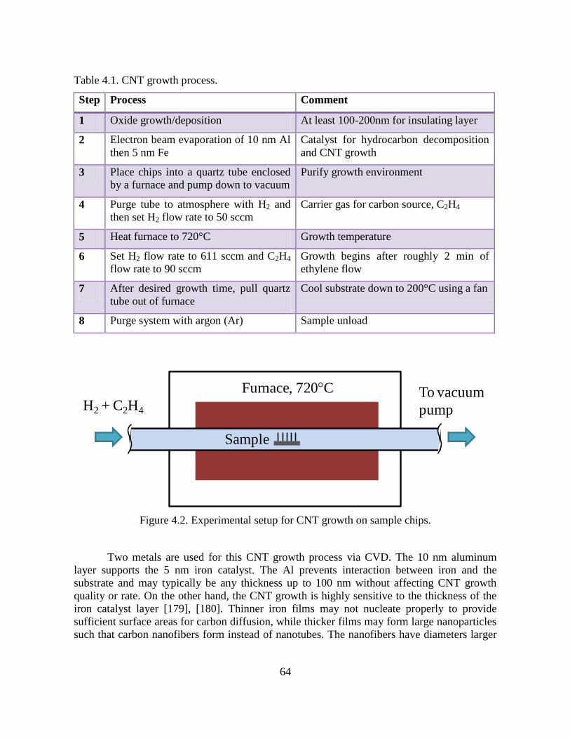
64
Table 4.1. CNT growth process.
Step Process Comment
1 Oxide growth/deposition At least 100-200nm for insulating layer
2 Electron beam evaporation of 10 nm Al
then 5 nm Fe
Catalyst for hydrocarbon decomposition
and CNT growth
3 Place chips into a quartz tube enclosed
by a furnace and pump down to vacuum
Purify growth environment
4 Purge tube to atmosphere with H2 and
then set H2 flow rate to 50 sccm
Carrier gas for carbon source, C2H4
5 Heat furnace to 720°C Growth temperature
6 Set H2 flow rate to 611 sccm and C2H4
flow rate to 90 sccm
Growth begins after roughly 2 min of
ethylene flow
7 After desired growth time, pull quartz
tube out of furnace
Cool substrate down to 200°C using a fan
8 Purge system with argon (Ar) Sample unload
H2 + C2H4
Furnace, 720°C
Sample
To vacuum
pump
Figure 4.2. Experimental setup for CNT growth on sample chips.
Two metals are used for this CNT growth process via CVD. The 10 nm aluminum
layer supports the 5 nm iron catalyst. The Al prevents interaction between iron and the
substrate and may typically be any thickness up to 100 nm without affecting CNT growth
quality or rate. On the other hand, the CNT growth is highly sensitive to the thickness of the
iron catalyst layer [179], [180]. Thinner iron films may not nucleate properly to provide
sufficient surface areas for carbon diffusion, while thicker films may form large nanoparticles
such that carbon nanofibers form instead of nanotubes. The nanofibers have diameters larger

65
than 100 nm, are mechanically unstable, and do not form any consistent pattern or forest like
CNTs. An example of carbon nanofibers may be seen below in Figure 4.3.
As mentioned in the previous section, different carbon source gases have different
decomposition temperatures. Experimental studies found ethylene (C2H4) to provide a balance
between growth temperature (720°C) and CNT quality. Hydrogen gas (H2) functions as a
carrier for the ethylene in the growth chamber. H2 presence also reduces the rate at which
carbon forms on the metal particle making it more likely that ordered CNTs will grow
compared to unordered nanofibers. Furthermore, CNTs from 5 μm to 50 μm in length may be
grown, where the growth begins roughly after 2 min of gas flow at the process temperature
and proceeds at a rate of approximately 5 μm/min. Results of successful CNT growth will be
discussed later in the context of the composite membrane used for encapsulation.
Figure 4.3. Carbon nanofiber growth resulting from thick Fe catalyst.
4.1.4 Proposed CNT/Polysilicon Composite
The relative ease at which CNTs may be grown serves as a foundation for a composite
structure using polysilicon as filler material. It has been demonstrated that when CNT forests
are combined with a filler material such as silicon nitride, the mechanical strength or high
temperature stability of the composite derives from the filler material [181]. Moreover, even if
the filler is insulating the composite film will remain electrically conductive. Furthermore,
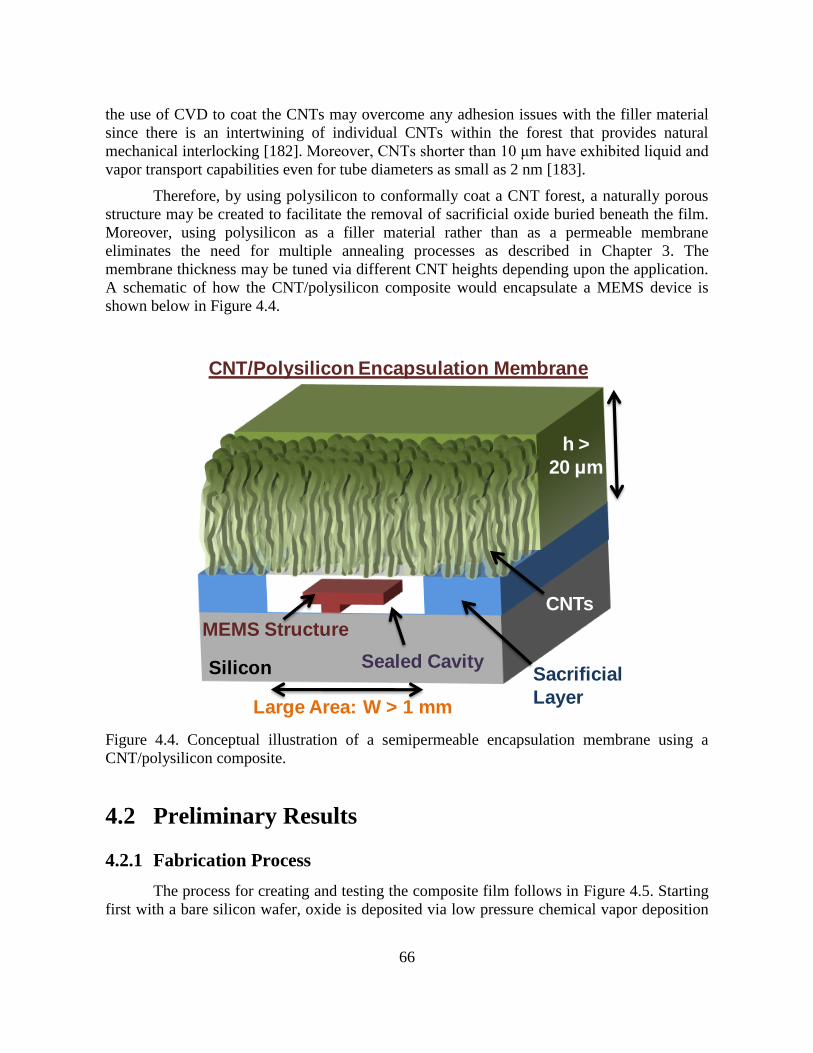
66
the use of CVD to coat the CNTs may overcome any adhesion issues with the filler material
since there is an intertwining of individual CNTs within the forest that provides natural
mechanical interlocking [182]. Moreover, CNTs shorter than 10 μm have exhibited liquid and
vapor transport capabilities even for tube diameters as small as 2 nm [183].
Therefore, by using polysilicon to conformally coat a CNT forest, a naturally porous
structure may be created to facilitate the removal of sacrificial oxide buried beneath the film.
Moreover, using polysilicon as a filler material rather than as a permeable membrane
eliminates the need for multiple annealing processes as described in Chapter 3. The
membrane thickness may be tuned via different CNT heights depending upon the application.
A schematic of how the CNT/polysilicon composite would encapsulate a MEMS device is
shown below in Figure 4.4.
h >
20 μm
Sacrificial
Layer
Sealed Cavity
Large Area: W > 1 mm
Silicon
CNT/Polysilicon Encapsulation Membrane
MEMS Structure
CNTs
Figure 4.4. Conceptual illustration of a semipermeable encapsulation membrane using a
CNT/polysilicon composite.
4.2 Preliminary Results
4.2.1 Fabrication Process
The process for creating and testing the composite film follows in Figure 4.5. Starting
first with a bare silicon wafer, oxide is deposited via low pressure chemical vapor deposition
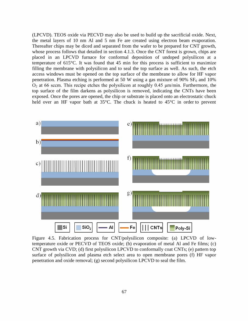
67
(LPCVD). TEOS oxide via PECVD may also be used to build up the sacrificial oxide. Next,
the metal layers of 10 nm Al and 5 nm Fe are created using electron beam evaporation.
Thereafter chips may be diced and separated from the wafer to be prepared for CNT growth,
whose process follows that detailed in section 4.1.3. Once the CNT forest is grown, chips are
placed in an LPCVD furnace for conformal deposition of undoped polysilicon at a
temperature of 615°C. It was found that 45 min for this process is sufficient to maximize
filling the membrane with polysilicon and to seal the top surface as well. As such, the etch
access windows must be opened on the top surface of the membrane to allow for HF vapor
penetration. Plasma etching is performed at 50 W using a gas mixture of 90% SF6 and 10%
O2 at 66 sccm. This recipe etches the polysilicon at roughly 0.45 μm/min. Furthermore, the
top surface of the film darkens as polysilicon is removed, indicating the CNTs have been
exposed. Once the pores are opened, the chip or substrate is placed onto an electrostatic chuck
held over an HF vapor bath at 35°C. The chuck is heated to 45°C in order to prevent
Figure 4.5. Fabrication process for CNT/polysilicon composite: (a) LPCVD of low-
temperature oxide or PECVD of TEOS oxide; (b) evaporation of metal Al and Fe films; (c)
CNT growth via CVD; (d) first polysilicon LPCVD to conformally coat CNTs; (e) pattern top
surface of polysilicon and plasma etch select area to open membrane pores (f) HF vapor
penetration and oxide removal; (g) second polysilicon LPCVD to seal the film.

68
condensation of HF or etching byproducts within the cavity. Various etch times have been
studied and will be reported later along with lateral undercut as a function of membrane
thickness. Finally, another polysilicon LPCVD of 45 min seals the film and the underlying
cavity as a possible wafer-level vacuum encapsulation process.
4.2.2 CNT Growth and Polysilicon Deposition
The CNT forests were grown consistently with repeatable heights for given growth
times. Specifically, to achieve 20 μm or 30 μm tall films the CNT growth occurred anywhere
from 4 min to 6 min. Figure 4.6 shows that forests of differing heights were vertically aligned
and dense. Close-up images of the CNT forest indicated that the CNTs are not perfectly
straight but actually wavy. This promotes the aforementioned mechanical interlocking of the
polysilicon coating on neighboring CNTs which is detailed in Figure 4.7.
As expected, the polysilicon thickness varied from top to bottom within the
membrane. The top 5 μm were fully sealed, whereas the bottom few μm exhibited thicknesses
of polysilicon ranging from 100 nm – 200 nm. The inherent porosity of the semi-permeable
membrane is quite clear. When sealed at the top, the film is impenetrable to HF vapor or other
materials. However, the top surface can be etched open to reveal the underlying pores. In the
first run of experiments etch windows were defined by manually painting photoresist on top
of the CNT/polysilicon composite. As mentioned above the top surface of the exposed area
darkened as polysilicon was removed by plasma etching. It was found that in order to
sufficiently open the pores in the membrane the minimum etch time was about 4 min, which
corresponded to removing nearly 2 μm of polysilicon. This can be seen below in Figure 4.8.
For preliminary testing to demonstrate the concept of the semi-permeable membrane, cavity
widths of 500 μm – 1500 μm were used.
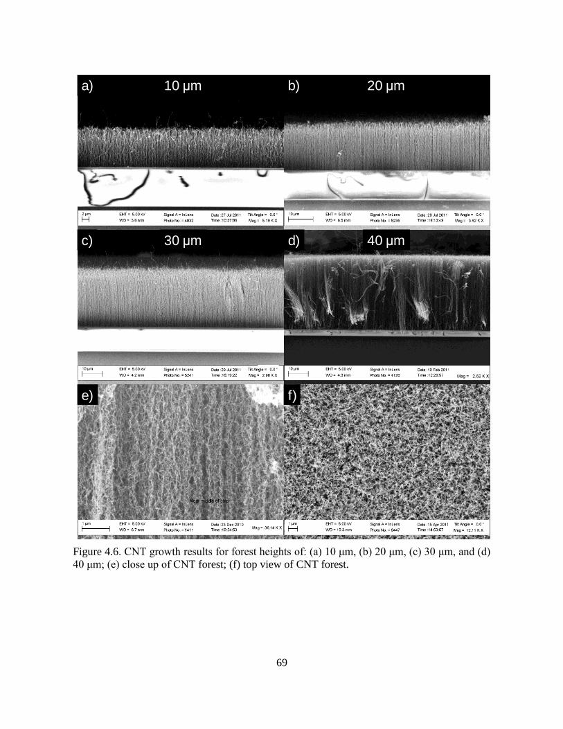
69
a) b)
c) d)
e)
10 μm 20 μm
30 μm 40 μm
f)
Figure 4.6. CNT growth results for forest heights of: (a) 10 μm, (b) 20 μm, (c) 30 μm, and (d)
40 μm; (e) close up of CNT forest; (f) top view of CNT forest.
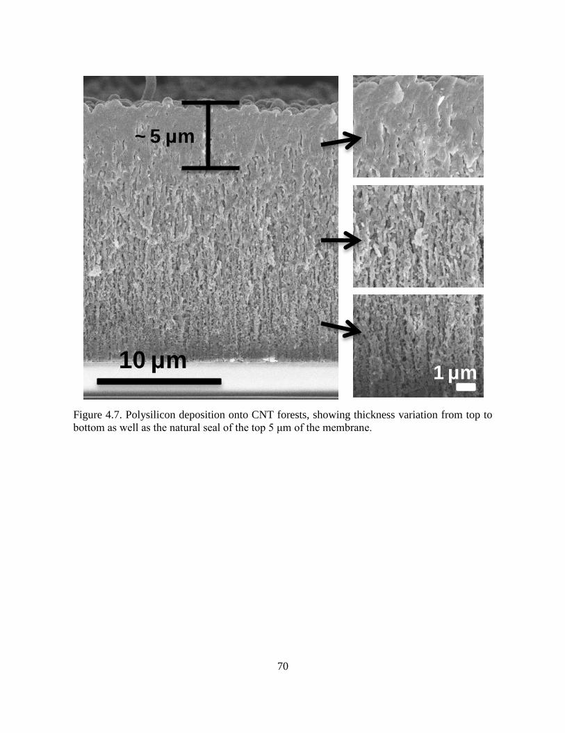
70
10 μm1 μm
~ 5 μm
Figure 4.7. Polysilicon deposition onto CNT forests, showing thickness variation from top to
bottom as well as the natural seal of the top 5 μm of the membrane.
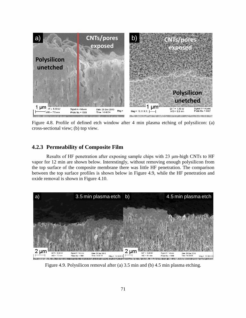
71
CNTs/pores exposed
Polysiliconunetched
CNTs/pores exposed
Polysiliconunetched
a) b)
Figure 4.8. Profile of defined etch window after 4 min plasma etching of polysilicon: (a)
cross-sectional view; (b) top view.
4.2.3 Permeability of Composite Film
Results of HF penetration after exposing sample chips with 23 μm-high CNTs to HF
vapor for 12 min are shown below. Interestingly, without removing enough polysilicon from
the top surface of the composite membrane there was little HF penetration. The comparison
between the top surface profiles is shown below in Figure 4.9, while the HF penetration and
oxide removal is shown in Figure 4.10.
a) b)3.5 min plasma etch 4.5 min plasma etch
Figure 4.9. Polysilicon removal after (a) 3.5 min and (b) 4.5 min plasma etching.
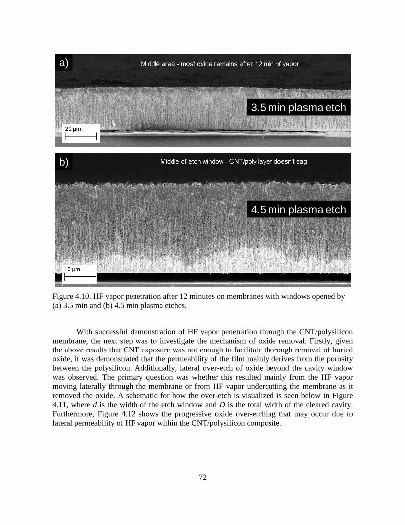
72
a)
b)
3.5 min plasma etch
4.5 min plasma etch
Figure 4.10. HF vapor penetration after 12 minutes on membranes with windows opened by
(a) 3.5 min and (b) 4.5 min plasma etches.
With successful demonstration of HF vapor penetration through the CNT/polysilicon
membrane, the next step was to investigate the mechanism of oxide removal. Firstly, given
the above results that CNT exposure was not enough to facilitate thorough removal of buried
oxide, it was demonstrated that the permeability of the film mainly derives from the porosity
between the polysilicon. Additionally, lateral over-etch of oxide beyond the cavity window
was observed. The primary question was whether this resulted mainly from the HF vapor
moving laterally through the membrane or from HF vapor undercutting the membrane as it
removed the oxide. A schematic for how the over-etch is visualized is seen below in Figure
4.11, where d is the width of the etch window and D is the total width of the cleared cavity.
Furthermore, Figure 4.12 shows the progressive oxide over-etching that may occur due to
lateral permeability of HF vapor within the CNT/polysilicon composite.
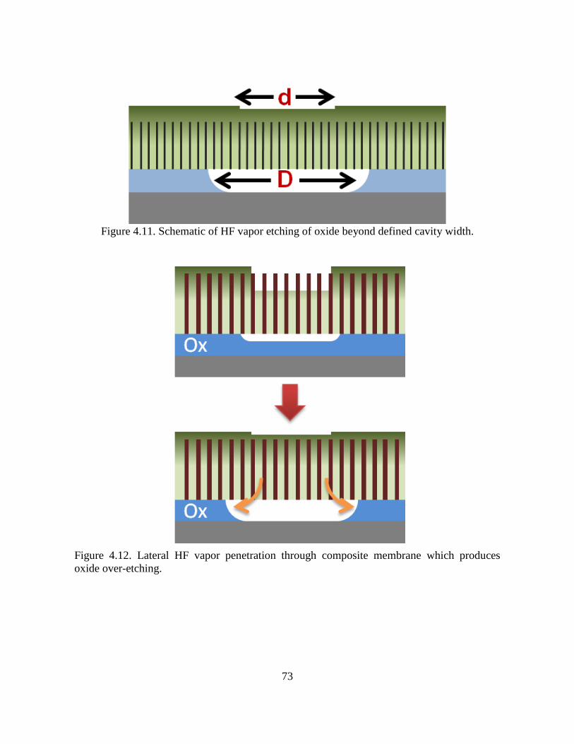
73
Figure 4.11. Schematic of HF vapor etching of oxide beyond defined cavity width.
Figure 4.12. Lateral HF vapor penetration through composite membrane which produces
oxide over-etching.
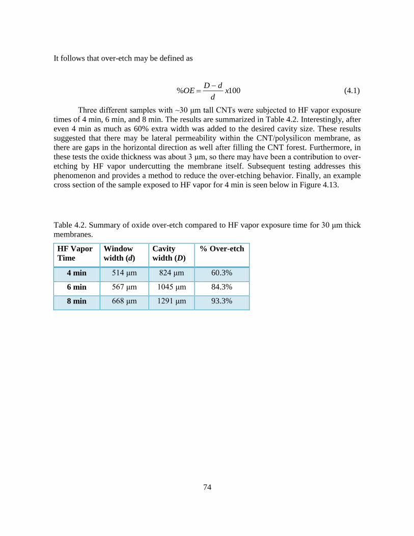
74
It follows that over-etch may be defined as
100% xd
dDOE
(4.1)
Three different samples with ~30 μm tall CNTs were subjected to HF vapor exposure
times of 4 min, 6 min, and 8 min. The results are summarized in Table 4.2. Interestingly, after
even 4 min as much as 60% extra width was added to the desired cavity size. These results
suggested that there may be lateral permeability within the CNT/polysilicon membrane, as
there are gaps in the horizontal direction as well after filling the CNT forest. Furthermore, in
these tests the oxide thickness was about 3 μm, so there may have been a contribution to over-
etching by HF vapor undercutting the membrane itself. Subsequent testing addresses this
phenomenon and provides a method to reduce the over-etching behavior. Finally, an example
cross section of the sample exposed to HF vapor for 4 min is seen below in Figure 4.13.
Table 4.2. Summary of oxide over-etch compared to HF vapor exposure time for 30 μm thick
membranes.
HF Vapor
Time
Window
width (d)
Cavity
width (D)
% Over-etch
4 min 514 μm 824 μm 60.3%
6 min 567 μm 1045 μm 84.3%
8 min 668 μm 1291 μm 93.3%
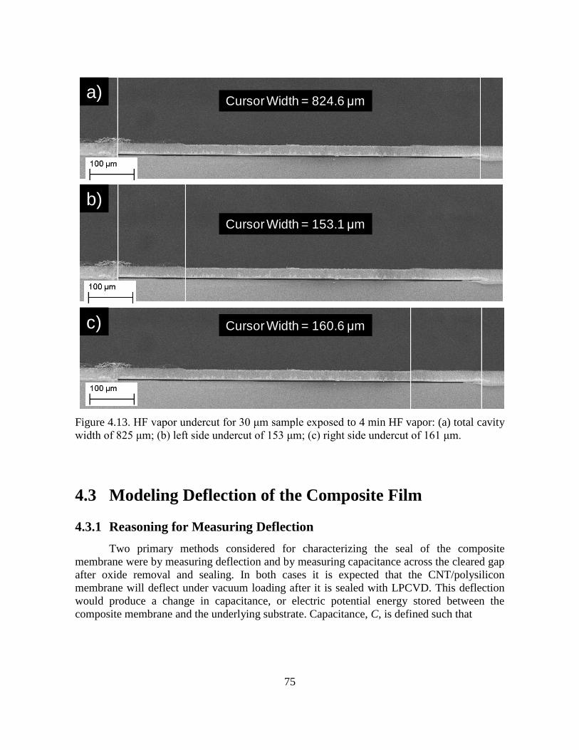
75
a)
b)
c)
Cursor Width = 824.6 μm
Cursor Width = 153.1 μm
Cursor Width = 160.6 μm
Figure 4.13. HF vapor undercut for 30 μm sample exposed to 4 min HF vapor: (a) total cavity
width of 825 μm; (b) left side undercut of 153 μm; (c) right side undercut of 161 μm.
4.3 Modeling Deflection of the Composite Film
4.3.1 Reasoning for Measuring Deflection
Two primary methods considered for characterizing the seal of the composite
membrane were by measuring deflection and by measuring capacitance across the cleared gap
after oxide removal and sealing. In both cases it is expected that the CNT/polysilicon
membrane will deflect under vacuum loading after it is sealed with LPCVD. This deflection
would produce a change in capacitance, or electric potential energy stored between the
composite membrane and the underlying substrate. Capacitance, C, is defined such that
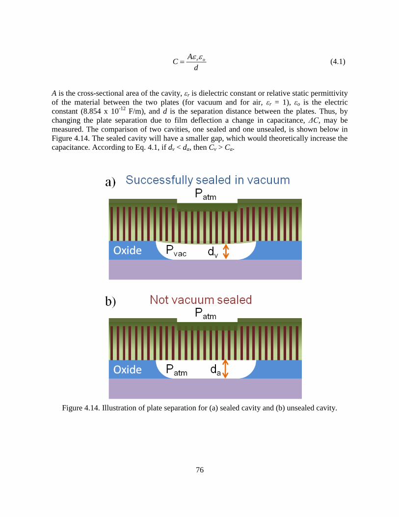
76
d
AC or (4.1)
A is the cross-sectional area of the cavity, εr is dielectric constant or relative static permittivity
of the material between the two plates (for vacuum and for air, εr = 1), εo is the electric
constant (8.854 x 10⁻¹²
F/m), and d is the separation distance between the plates. Thus, by
changing the plate separation due to film deflection a change in capacitance, ΔC, may be
measured. The comparison of two cavities, one sealed and one unsealed, is shown below in
Figure 4.14. The sealed cavity will have a smaller gap, which would theoretically increase the
capacitance. According to Eq. 4.1, if dv < da, then Cv > Ca.
Figure 4.14. Illustration of plate separation for (a) sealed cavity and (b) unsealed cavity.

77
A sample plot of capacitance vs. plate separation, e.g. oxide thickness, is shown below in
Figure 4.15. Thus, inducing a deflection of 8 μm in a square plate measured at 1500 μm x
1500 μm will only produce a ΔC of roughly 2.5 x 10⁻⁵
pF. This value is extremely small and
exceeds the sensitivity of equipment available to carry out such tests. Therefore, measuring
capacitance as a function of the film deflection was not pursued.
0.00E+00
5.00E-06
1.00E-05
1.50E-05
2.00E-05
2.50E-05
3.00E-05
3.50E-05
4.00E-05
4.50E-05
4 6 8 10 12 14 16
Cap
acit
ance
(pF)
Plate separation (μm)
500μm x 500μm
750μm x 750μm
1500μm x 1500μm
1250μm x 1250μm
1500μm x 1500μm
Figure 4.15. Theoretical capacitance for different cavity sizes as a function of plate separation
or oxide thickness.
A more direct method of measurement is to profile the actual deflection of the
composite membrane across the cavity. This is done using an Alpha-Step profilometer which
scans and measures the topography along a surface using a stylus with a 5 μm radius tip. The
measured deflection can therefore be correlated to the pressure inside the cavity. The details
of how to design for and measure deflection follow in the next section.
4.3.2 Theory for Plate Deflection
After demonstrating the proof of concept and the successful HF vapor penetration
through the CNT/polysilicon composite, theoretical modeling of deflection of the membrane
under vacuum loading was performed. As in the case of permeable polysilicon membranes in
Chapter 3, the following assumptions were used for the membrane:
78
The plate material is linear elastic
The plate material is homogenous and isotropic
Since the plate thickness is small compared to lateral dimensions, normal stress in
the transverse direction to deflection may be neglected
Loads are applied in a direction perpendicular to the center plane of the plate
Because the composite film should be 99% comprised of polysilicon, it’s estimated
that Young’s Modulus of Elasticity, E, derives mainly from that material such that for
polysilicon, values of E = 169 GPa and Poisson’s ratio ν = 0.22 are used [135]. However, later
in designing the sizes of etch windows the effects of porosity on E will be considered.
Modeling the maximum deflection, wmax, and maximum stress, σmax, under a uniform
load of p in the film of thickness t follows from classical theory of flat plate bending, where
D
pbw
4
max (4.2)
2
3
112
EtD (4.3)
2
2
1max,t
pbx (4.4)
Eqs. 4.2 through 4.4 apply to rectangular or square plates which are clamped around all edges,
shown in Figure 3.5. The values of α and β1 depend on the ratio between side lengths 2b to 2a
based on Roark’s Formulas for Stress and Strain [137]. In the case of a square membrane with
a = b, and using ν = 0.22, the maximum deflection and stress become
3
4
max 01443.0Et
pbw (4.5)
2
2
max, 2312.1t
pbx (4.6)
For rectangular membranes, the ratio of 2b/2a increases beyond 1, where 2b is the longer side
of the membrane at a specific value, e.g. 3000 μm, and 2a is the shorter side which ranges
anywhere from 500 μm to 3000 μm. As 2b/2a increases the coefficients in the above
equations also increase. For example, for a rectangle with one side twice as long as the other,
wmax increases by a factor of 2 while σmax increases by a factor of 1.5 as compared with a
square membrane with width of a. Therefore, square plates in finite element analysis (FEA)
were analyzed as a ‘best-case’ scenario for rectangular plates.
In addition, circular plates were considered for designing etch windows on the
CNT/polysilicon composite. It follows that for a circular clamped plate of diameter c,
79
D
pcw
64
4
max (4.7)
Plugging in D from Eq. 4.2 yields
3
4
max 01115.0Et
pcw (4.8)
Comparing Eq. 4.8 to Eq. 4.5 shows that for a circular window with a diameter equivalent to
the length of a square window, the circular membrane will deflect 23% less at its center as
compared with a square membrane at its center. This is agreeable as the circular window
would have less total area compared to the square in this case. Thus, in a larger scope for any
given size cavity a circular window is preferred to minimize film deflection and prevent the
membrane from touching down onto the underlying substrate. However, most of the analysis
here was performed with square cavities.
4.3.3 Membrane Deflection Calculations and FEA
Using Eq. 4.5 a variety of predicted deflections under vacuum loading (p = 101.3 kPa)
for different square membrane sizes as a function of membrane or CNT height were
calculated. This was helpful for determining the allowable ranges of designs where the
expected film deflection under vacuum does not exceed the oxide thickness which may be up
to 10 μm thick or greater using quick TEOS + RTA deposition techniques developed in the
preceding chapter. A conservative estimate for the stiffness of the membrane as 85 GPa, half
that of bulk polysilicon, was used to incorporate possible weakness due to the porosity of the
membrane. The results may be seen below in Figure 4.16.
The results show that for larger areas spanning more than 1000 μm width the CNT
height should be above 20 μm to keep film deflection under 10 μm. However, at the same
time it must be considered that the top surface of the CNT/polysilicon membrane exhibits a
roughness on the order of 1-2 μm. This top surface could be planarized with TEOS but
deflection predictions for a given CNT height and cavity width would change. Thus, a simpler
solution is to design the devices such that predicted deflections are anywhere from 7.5 μm to
10 μm so that they stand out from the inherent roughness in the film.
It’s also noted here that film deflection may be drastically reduced by using silicon
nitride as a filler material since its modulus of elasticity is 222 GPa. However, generating
measurable film deflections of less than 10 μm for this alternative composite requires the
cavities to be no wider than 200 μm, even for short CNTs with heights also less than 10 μm.
While silicon nitride is a possible future alternative, it was not used in testing since the goal
for demonstrating successful encapsulation was to observe large deflections.
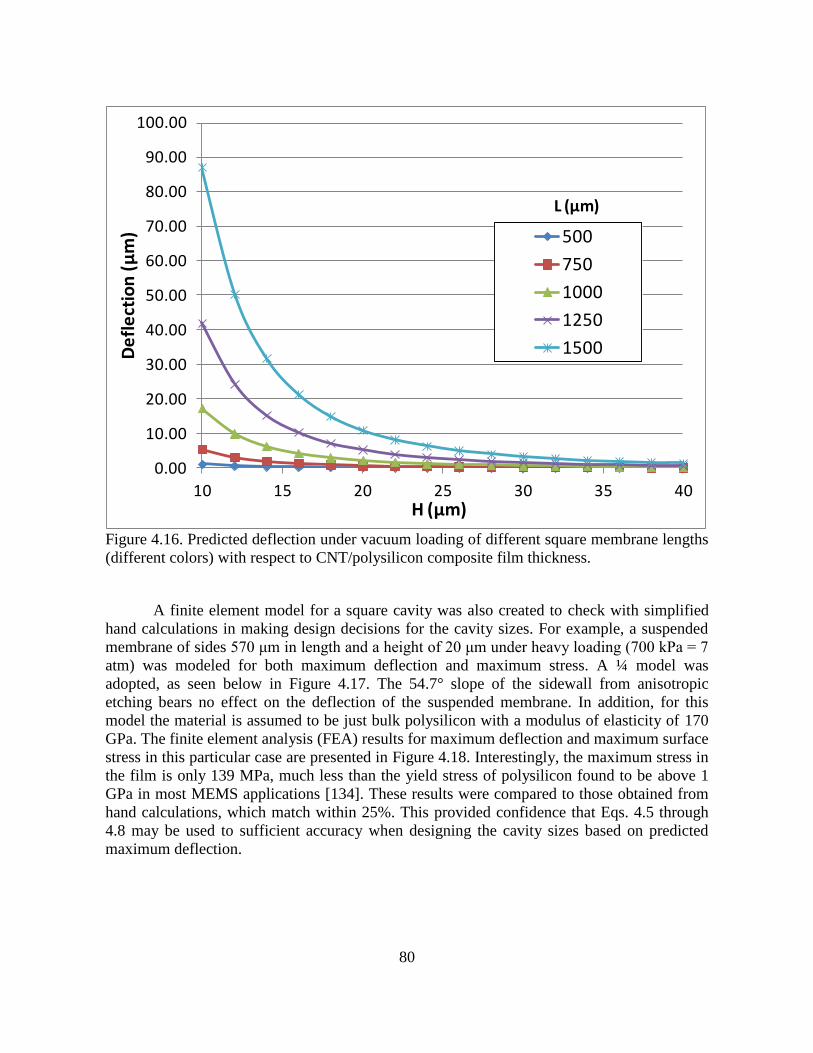
80
0.00
10.00
20.00
30.00
40.00
50.00
60.00
70.00
80.00
90.00
100.00
10 15 20 25 30 35 40
De
fle
ctio
n (
μm
)
H (μm)
500
750
1000
1250
1500
L (µm)
Figure 4.16. Predicted deflection under vacuum loading of different square membrane lengths
(different colors) with respect to CNT/polysilicon composite film thickness.
A finite element model for a square cavity was also created to check with simplified
hand calculations in making design decisions for the cavity sizes. For example, a suspended
membrane of sides 570 μm in length and a height of 20 μm under heavy loading (700 kPa = 7
atm) was modeled for both maximum deflection and maximum stress. A ¼ model was
adopted, as seen below in Figure 4.17. The 54.7° slope of the sidewall from anisotropic
etching bears no effect on the deflection of the suspended membrane. In addition, for this
model the material is assumed to be just bulk polysilicon with a modulus of elasticity of 170
GPa. The finite element analysis (FEA) results for maximum deflection and maximum surface
stress in this particular case are presented in Figure 4.18. Interestingly, the maximum stress in
the film is only 139 MPa, much less than the yield stress of polysilicon found to be above 1
GPa in most MEMS applications [134]. These results were compared to those obtained from
hand calculations, which match within 25%. This provided confidence that Eqs. 4.5 through
4.8 may be used to sufficient accuracy when designing the cavity sizes based on predicted
maximum deflection.
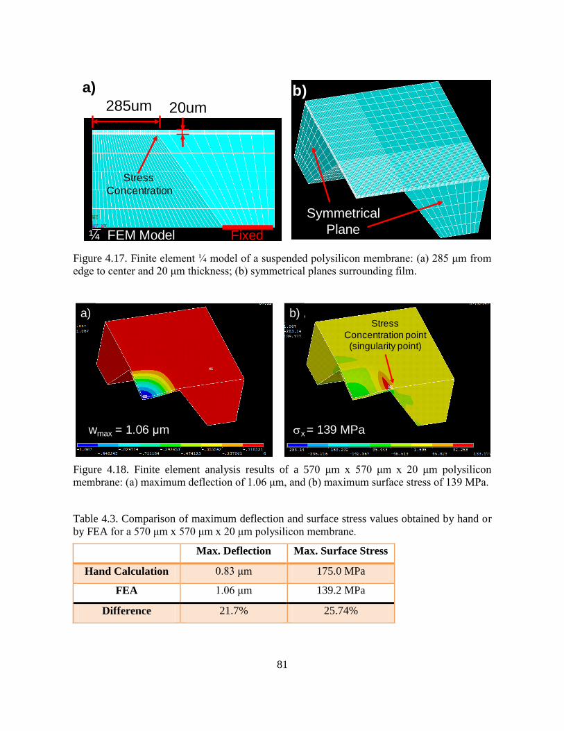
81
¼ FEM Model
20um285um
Fixed
Stress
Concentration
Symmetrical
Plane
a) b)
Figure 4.17. Finite element ¼ model of a suspended polysilicon membrane: (a) 285 μm from
edge to center and 20 μm thickness; (b) symmetrical planes surrounding film.
wmax = 1.06 μm x = 139 MPa
a) b)Stress
Concentration point(singularity point)
Figure 4.18. Finite element analysis results of a 570 μm x 570 μm x 20 μm polysilicon
membrane: (a) maximum deflection of 1.06 μm, and (b) maximum surface stress of 139 MPa.
Table 4.3. Comparison of maximum deflection and surface stress values obtained by hand or
by FEA for a 570 μm x 570 μm x 20 μm polysilicon membrane.
Max. Deflection Max. Surface Stress
Hand Calculation 0.83 μm 175.0 MPa
FEA 1.06 μm 139.2 MPa
Difference 21.7% 25.74%
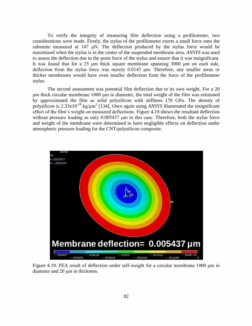
82
To verify the integrity of measuring film deflection using a profilometer, two
considerations were made. Firstly, the stylus of the profilometer exerts a small force onto the
substrate measured at 147 μN. The deflection produced by the stylus force would be
maximized when the stylus is in the center of the suspended membrane area. ANSYS was used
to assess the deflection due to the point force of the stylus and ensure that it was insignificant.
It was found that for a 25 μm thick square membrane spanning 3000 μm on each side,
deflection from the stylus force was merely 0.0143 μm. Therefore, any smaller areas or
thicker membranes would have even smaller deflection from the force of the profilometer
stylus.
The second assessment was potential film deflection due to its own weight. For a 20
μm thick circular membrane 1000 μm in diameter, the total weight of the film was estimated
by approximated the film as solid polysilicon with stiffness 170 GPa. The density of
polysilicon is 2.33x10⁻¹⁸
kg/μm3 [134]. Once again using ANSYS illuminated the insignificant
effect of the film’s weight on measured deflections. Figure 4.19 shows the resultant deflection
without pressure loading as only 0.005437 μm in this case. Therefore, both the stylus force
and weight of the membrane were determined to have negligible effects on deflection under
atmospheric pressure loading for the CNT/polysilicon composite.
Membrane deflection= 0.005437 μm
Figure 4.19. FEA result of deflection under self-weight for a circular membrane 1000 μm in
diameter and 20 μm in thickness.
83
4.3.4 Design Methodology
Having confirmed the possibility of using simplified deflection and stress equations to
predict membrane behavior under vacuum load, a range of allowable designs for cavities was
generated. The primary guide to this process was that the oxide thickness limits the maximum
deflection of the membrane. Therefore, one may set the deflection to any desired value, such
as 7.5 μm, and determine the necessary cavity size for a given membrane height or vice versa.
Given the uncertainty of the actual modulus of elasticity for the CNT/polysilicon
composite, upper and lower bounds for each combination of membrane thickness and oxide
thickness were developed. For the upper bound limit, polysilicon is assumed to fully fill the
CNT forest without voids. This was not observed in previous results but served as a ‘best case
scenario’ in which the composite membrane derives its stiffness from a representative
polysilicon film of the same thickness as the CNT height. The Young’s modulus used is 170
GPa. However, in reality due to the natural porosity and voids within the film the effective
Young’s modulus should be less than 170 GPa. The lower bound limit assumes that
polysilicon does not sufficiently fill the CNT forest and the strength of the film will at least
come from the top 5 μm which have been previously shown to fill completely with
polysilicon. However, it will be very difficult to estimate the Young’s modulus of the rest of
the CNT/polysilicon composite film.
Table 4.4 summarizes the upper bounds for square and circular cavity dimensions as a
function of the composite membrane thickness. The maximum deflection in each case is set to
be 7.5 μm. For all membrane heights the minimum cavity width is 577 μm for a square and
748 μm for a circle, since the lower bound only depends on the 5 μm of the forest filling with
polysilicon. Given the range of CNTs that may be grown, the dark-field photomask used to
define the etch windows incorporated cavity widths ranging from 250 μm to 3000 μm by
increments of 250 μm. Because of the large feature sizes, this mask was printed on a
transparency using an inkjet printer, then cut out and taped onto a 7” x 7” glass plate.
Therefore, for a batch of separate chips on which CNTs were grown, each chip could be
patterned with a different etch window size and tested for deflection by measuring the surface
profile after sealing with the second LPCVD of polysilicon.

84
Table 4.4. Upper bounds for square and circular cavity sizes as a function of CNT height for
7.5 μm maximum deflection.
CNT/Membrane
Height
Max. Cavity
Width (Square)
Max. Cavity
Diameter (Circle)
20 μm 1.63 mm 2.11 mm
25 μm 1.93 mm 2.50 mm
30 μm 2.21 mm 2.86 mm
35 μm 2.48 mm 3.21 mm
40 μm 2.75 mm 3.56 mm
4.4 Process Characterization
4.4.1 Over-Etch Behavior
It was found previously that for 30 μm tall CNTs there was significant lateral over-
etch for different HF vapor exposure times. Subsequently, 20 μm thick membranes were
tested against over-etch, and it was found that the membranes with shorter distance had much
lower degrees of undercut. A short summary of these results is found in Table 4.5, while a
cross-sectional view of the controlled lateral etch for one of the samples exposed to HF vapor
for 8 min can be seen in Figure 4.20(a). Furthermore, the edge of the oxide layer, shown in
Figure 4.20(b), illustrates a different morphology than for a typical wet etch process since the
oxide is attacked from the side and above due to lateral permeability in the composite
membrane.
In addition, over-etch for 20 μm and 30 μm tall composite films are compared in
Figure 4.21, clearly showing the huge reduction in lateral undercut for a membrane
constructed from a shorter CNT forest. These results illustrate one trade-off in designing the
encapsulation membrane, as the cavity width must be reduced accordingly to compensate for
over-etch in cases where a thicker membrane is required (e.g. larger areas for certain MEMS
devices). Another option would be to incorporate either a hard mask underneath the
encapsulation membrane or to pattern the membrane itself. This will be discussed in the next
chapter.
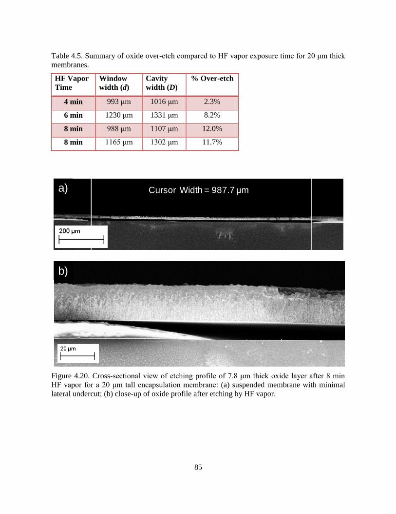
85
Table 4.5. Summary of oxide over-etch compared to HF vapor exposure time for 20 μm thick
membranes.
HF Vapor
Time
Window
width (d)
Cavity
width (D)
% Over-etch
4 min 993 μm 1016 μm 2.3%
6 min 1230 μm 1331 μm 8.2%
8 min 988 μm 1107 μm 12.0%
8 min 1165 μm 1302 μm 11.7%
a)
b)
Cursor Width = 987.7 μm
Figure 4.20. Cross-sectional view of etching profile of 7.8 μm thick oxide layer after 8 min
HF vapor for a 20 μm tall encapsulation membrane: (a) suspended membrane with minimal
lateral undercut; (b) close-up of oxide profile after etching by HF vapor.
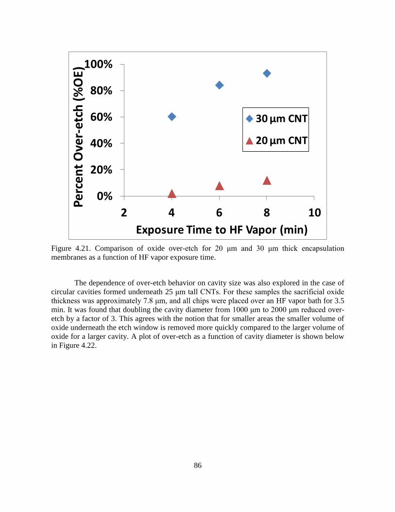
86
0%
20%
40%
60%
80%
100%
2 4 6 8 10
Pe
rce
nt
Ove
r-e
tch
(%
OE)
Exposure Time to HF Vapor (min)
30 μm CNT
20 μm CNT
Figure 4.21. Comparison of oxide over-etch for 20 μm and 30 μm thick encapsulation
membranes as a function of HF vapor exposure time.
The dependence of over-etch behavior on cavity size was also explored in the case of
circular cavities formed underneath 25 μm tall CNTs. For these samples the sacrificial oxide
thickness was approximately 7.8 μm, and all chips were placed over an HF vapor bath for 3.5
min. It was found that doubling the cavity diameter from 1000 μm to 2000 μm reduced over-
etch by a factor of 3. This agrees with the notion that for smaller areas the smaller volume of
oxide underneath the etch window is removed more quickly compared to the larger volume of
oxide for a larger cavity. A plot of over-etch as a function of cavity diameter is shown below
in Figure 4.22.

87
0.0%
2.0%
4.0%
6.0%
8.0%
10.0%
12.0%
14.0%
16.0%
18.0%
750 1250 1750 2250 2750
Pe
rce
nt O
ve
r-e
tch
(%
OE
)
Defined cavity diameter (μm)
Figure 4.22. Oxide over-etch for 25 μm thick membranes as a function of defined cavity
diameter for circular etch windows.
4.4.2 Encapsulation and Deflection Under Vacuum
The second polysilicon deposition is likely to fill up the pores quickly since the first
polysilicon deposition should fill up the top section while the plasma etching process only
opens the very top portion of the membrane pores. This is a good feature as it is desirable that
the second polysilicon deposition won’t alter the original geometry of the MEMS devices
inside the cavity during the deposition process. In addition, it’s noted that defining the etch
window creates a step height of roughly 2-3 μm on top of the membrane after the first
polysilicon deposition. This is not an issue for the sealing step. However, for subsequent
post-encapsulation processing a planar surface may be desirable. In this case the top surface
of the membrane may be smoothened with a self-planarizing TEOS deposition step. This
permits easier post-seal processing steps such as opening of electrical contacts. SEM
photographs show the sealing by LPCVD in Figure 4.23.
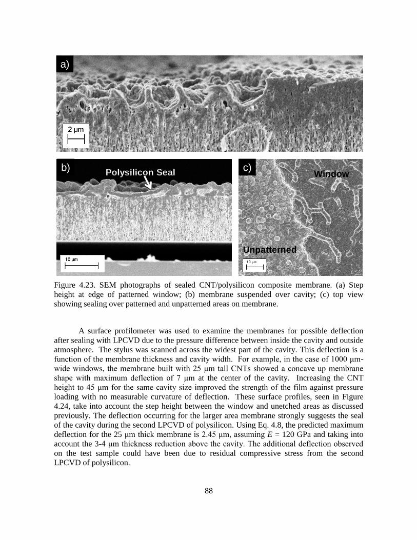
88
a)
b) c)Window
Unpatterned
Polysilicon Seal
Figure 4.23. SEM photographs of sealed CNT/polysilicon composite membrane. (a) Step
height at edge of patterned window; (b) membrane suspended over cavity; (c) top view
showing sealing over patterned and unpatterned areas on membrane.
A surface profilometer was used to examine the membranes for possible deflection
after sealing with LPCVD due to the pressure difference between inside the cavity and outside
atmosphere. The stylus was scanned across the widest part of the cavity. This deflection is a
function of the membrane thickness and cavity width. For example, in the case of 1000 μm-
wide windows, the membrane built with 25 μm tall CNTs showed a concave up membrane
shape with maximum deflection of 7 μm at the center of the cavity. Increasing the CNT
height to 45 μm for the same cavity size improved the strength of the film against pressure
loading with no measurable curvature of deflection. These surface profiles, seen in Figure
4.24, take into account the step height between the window and unetched areas as discussed
previously. The deflection occurring for the larger area membrane strongly suggests the seal
of the cavity during the second LPCVD of polysilicon. Using Eq. 4.8, the predicted maximum
deflection for the 25 μm thick membrane is 2.45 μm, assuming E = 120 GPa and taking into
account the 3-4 μm thickness reduction above the cavity. The additional deflection observed
on the test sample could have been due to residual compressive stress from the second
LPCVD of polysilicon.
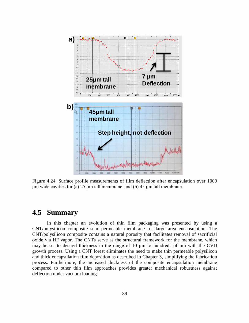
89
25μm tall
membrane
a)
45μm tall
membrane
b)
Step height, not deflection
7 μm
Deflection
Figure 4.24. Surface profile measurements of film deflection after encapsulation over 1000
μm wide cavities for (a) 25 μm tall membrane, and (b) 45 μm tall membrane.
4.5 Summary
In this chapter an evolution of thin film packaging was presented by using a
CNT/polysilicon composite semi-permeable membrane for large area encapsulation. The
CNT/polysilicon composite contains a natural porosity that facilitates removal of sacrificial
oxide via HF vapor. The CNTs serve as the structural framework for the membrane, which
may be set to desired thickness in the range of 10 μm to hundreds of μm with the CVD
growth process. Using a CNT forest eliminates the need to make thin permeable polysilicon
and thick encapsulation film deposition as described in Chapter 3, simplifying the fabrication
process. Furthermore, the increased thickness of the composite encapsulation membrane
compared to other thin film approaches provides greater mechanical robustness against
deflection under vacuum loading.
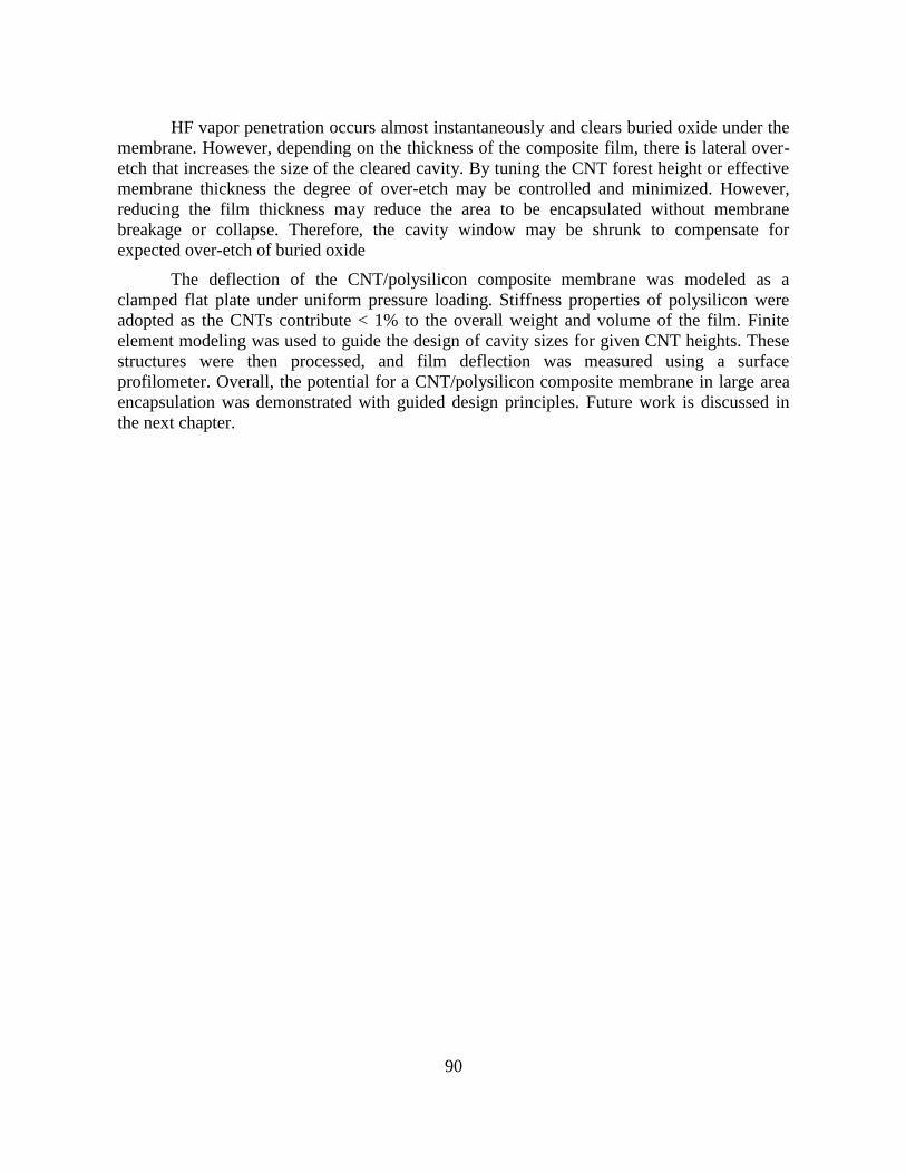
90
HF vapor penetration occurs almost instantaneously and clears buried oxide under the
membrane. However, depending on the thickness of the composite film, there is lateral over-
etch that increases the size of the cleared cavity. By tuning the CNT forest height or effective
membrane thickness the degree of over-etch may be controlled and minimized. However,
reducing the film thickness may reduce the area to be encapsulated without membrane
breakage or collapse. Therefore, the cavity window may be shrunk to compensate for
expected over-etch of buried oxide
The deflection of the CNT/polysilicon composite membrane was modeled as a
clamped flat plate under uniform pressure loading. Stiffness properties of polysilicon were
adopted as the CNTs contribute < 1% to the overall weight and volume of the film. Finite
element modeling was used to guide the design of cavity sizes for given CNT heights. These
structures were then processed, and film deflection was measured using a surface
profilometer. Overall, the potential for a CNT/polysilicon composite membrane in large area
encapsulation was demonstrated with guided design principles. Future work is discussed in
the next chapter.
91
Chapter 5
Conclusions and Future Work
5.1 Conclusions
In this work, two thin film encapsulation approaches to the packaging of MEMS
devices were explored. Packaging is a critical and often overlooked component of designing,
fabricating, and commercializing MEMS devices. Depending on the application, different
packaging requirements apply, but generally the function of MEMS packaging is to provide
mechanical sustentation and protection from the environment. In addition, thermal
management and hermetic sealing often play large roles in packaging as some MEMS devices
must sustain harsh environments.
Thin film encapsulation offers potential advantages over wafer-to-wafer bonding,
namely the reduction of materials costs, increased usable area on device wafers due to the
elimination of the seal ring, greater throughput in testing, compatibility with MEMS
processing, and avoidance of aligning two separate substrates. Moreover, it is possible to
continue fabrication after encapsulation with a thin film process,
Permeable polysilicon was used as a thin film membrane for encapsulation. In order to
make the film permeable dopants from the underlying oxide were driven into the polysilicon
with high temperature annealing at 950°C. Thereafter the film became penetrable by HF
vapor which could remove the buried oxide and create a cavity under the suspended
membrane within 10 minutes. Additionally, FEA was used to determine deformation of the
encapsulation membrane due to pressure differences between the packaging cavity and the
external environment. It was determined that a 15 μm thick sealing layer of oxide would
provide enough support against deflection under vacuum loading. To make this possible, a
process of incremental TEOS deposition steps of 2.5 μm and intermediate rapid thermal
annealing at 900°C was developed to generate thick TEOS layers without cracking due to
residual stress.
The concept of using permeable polysilicon inspired the use of a composite membrane
for large area encapsulation. Carbon nanotubes were grown on top of sacrificial oxide layers
and coated with polysilicon to form composite membranes ranging in thickness from 10 μm
to 50 μm. This approach eliminated the requirement to construct the permeable polysilicon, as
the composite membrane exhibits a natural porosity after polysilicon coats the CNT forest.
Futhermore, it is rather fast (less than 10 minutes of CVD) to synthesize the CNT forest with
tens of micrometers in thickness to provide a thick encapsulation cap. The semi-permeable
membrane was also modeled with FEA to predict film deflection under vacuum loading.

92
Furthermore, the HF etching behavior was characterized, and it was observed that over-etch
of buried oxide may be reduced from greater than 80% of the defined cavity width to less than
10%. This was accomplished by decreasing the height of the CNTs from 30 μm to 20 μm,
thereby limiting lateral penetration by HF vapor through the composite membrane. Lastly, it
was demonstrated that cavities of widths greater than 1000 μm could withstand deflection
under vacuum load with an increased membrane thickness of 45 μm.
A summary of the key parameters of the two thin film encapsulation techniques in this
work is found below in Table 5.1. The permeable polysilicon with TEOS method and
CNT/polysilicon composite are also referenced against previous work using permeable
polysilicon. It is seen that the primary improvement in thin film encapsulation is attained by
moving beyond the limitations of pure thin films and increasing the thickness of the sealing
membranes. In addition, the CNT/polysilicon composite eliminates the need to dope thin
polysilicon films by annealing. Future work in the following sections details how the
CNT/polysilicon membrane may be further characterized and tested.
Table 5.1. Comparison of thin film encapsulation approaches.
Permeable Polysilicon
[132], [143]
Permeable
Polysilicon + TEOS
CNT/Polysilicon
Composite
# of Steps to Form
Seal on Planar
Oxide Layer
11 9 7
Maximum Process
Temperature
1000 °C 950 °C 720 °C
Permeable Layer
and Thickness
Doped polysilicon
100 – 150 nm
Doped polysilicon
< 300 nm
Permeable and
sealing layers are the
same structure;
10 – 100 μm Sealing Layer and
Thickness
Silicon Nitride
1 – 2 μm
TEOS
can be > 10 μm
Largest Cavity
Width
< 1 mm > 1 mm > 1 mm
Overall, the evolution of wafer-level encapsulation using thin films has provided a
larger sandbox for designing and packaging MEMS devices. Here areas spanning more than 1
mm on each side were generated using both permeable polysilicon and the CNT/polysilicon
composite. However, the latter approach functions as both a more process-friendly alternative
and a stronger sealing structure. The groundwork for such a packaging scheme has been
established, and the versatility of the composite encapsulation membrane with respect to size
and thickness paves the road for a wide range of applications and testing of MEMS devices
sealed by such a process.
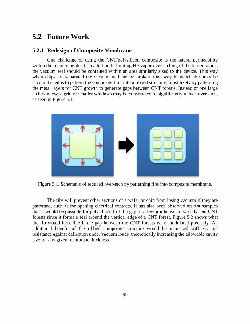
93
5.2 Future Work
5.2.1 Redesign of Composite Membrane
One challenge of using the CNT/polysilicon composite is the lateral permeability
within the membrane itself. In addition to limiting HF vapor over-etching of the buried oxide,
the vacuum seal should be contained within an area similarly sized to the device. This way
when chips are separated the vacuum will not be broken. One way in which this may be
accomplished is to pattern the composite film into a ribbed structure, most likely by patterning
the metal layers for CNT growth to generate gaps between CNT forests. Instead of one large
etch window, a grid of smaller windows may be constructed to significantly reduce over-etch,
as seen in Figure 5.1.
Figure 5.1. Schematic of reduced over-etch by patterning ribs into composite membrane.
The ribs will prevent other sections of a wafer or chip from losing vacuum if they are
patterned, such as for opening electrical contacts. It has also been observed on test samples
that it would be possible for polysilicon to fill a gap of a few μm between two adjacent CNT
forests since it forms a seal around the vertical edge of a CNT forest. Figure 5.2 shows what
the rib would look like if the gap between the CNT forests were modulated precisely. An
additional benefit of the ribbed composite structure would be increased stiffness and
resistance against deflection under vacuum loads, theoretically increasing the allowable cavity
size for any given membrane thickness.

94
Figure 5.2. Hypothetical gap filling between CNT forests by polysilicon.
5.2.2 Characterizing Sealing Conditions
Encapsulation by the CNT/polysilicon membrane was tested by measuring for
curvature after the second LPCVD of polysilicon which seals the membrane. However, it
would be beneficial to observe deflection changes on a single chip by controlling the outside
pressure. This type of approach requires a small vacuum chamber which is also transparent. A
laser interferometer or laser displacement meter may then be used to generate a surface profile
without direct contact by a stylus such as with an alpha-stepper. An example design for a
small test chamber is seen below in Figure 5.3. The pressure of the enclosed environment
within the chamber may then be changed at will with connection to a vacuum pump. So long
as the device is sealed at low or near-vacuum pressure, the pressure difference and resulting
change in deflection of the encapsulation membrane between inside the cavity and inside the
chamber could be monitored in real time. A similar apparatus or setup could also be designed
to test the hermeticity of the CNT/polysilicon composite against both gas and liquid leakage.
Since in some cases the deflection of the composite membrane may be difficult to
detect or control, an alternative approach would be to monitor deflection of a backside
membrane. This could be performed on an SOI wafer, or a nitride layer could be placed onto
the silicon substrate before oxide deposition. In either case, deep reactive ion etching through
the underside of the silicon wafer would be necessary. This concept is shown in Figure 5.4.
95
70 mm
50 mm
3.2 mm
2.5 mm
20 mm
20 mm
2.5 mm
Glass window
Figure 5.3. Sample design for a small vacuum test chamber used in conjunction with a laser
interferometer or laser displacement meter.
Figure 5.4. Backside membrane of silicon or silicon nitride used to characterize internal cavity
pressure based on measured deflection.
5.2.3 Process Flow for Integrated MEMS Device
The ultimate long-term goal of this work is to incorporate and test various MEMS
devices within the CNT/polysilicon encapsulation scheme. A simple resonator or pressure
gauge may be fabricated on a silicon wafer, enclosed by sacrificial oxide, then released and
sealed within the cavity. Polysilicon may be used as a conductive layer for patterning
electrical contacts away from the cavity area. Using the ribbed structure proposed above, the
encapsulation membrane may be patterned or opened without breaking the vacuum seal over
the device cavity. An outline for this fabrication process follows in Figure 5.5 in which a
secondary material such as TEOS or thick photoresist is used to planarize the substrate after
encapsulation.

96
Figure 5.5. General process for encapsulating a simple MEMS device and opening electrical
contacts without breaking vacuum.
For this proposed process, the MEMS structure is first fabricated on a silicon wafer. A
thin conductive layer of polysilicon is then deposited with LPCVD to provide electrical
interconnection to the device. Next, a thick TEOS layer is deposited with incremental RTA as
previously demonstrated to planarize the substrate and enclose the MEMS device within a
sacrificial layer. The corresponding metal layers of Al and Fe may be evaporated and
patterned into a grid of squares separated by a few μm. After CVD growth of CNTs and the
first LPCVD of polysilicon to fill the CNT forest, the rib structure should form with solid
polysilicon filling those gaps across the membrane and isolating the seal of each CNT forest.

97
After the composite is formed the window for HF vapor penetration may be patterned
with SF6 + O2 plasma etching. The substrate is then exposed to HF vapor for a timed etch (4-8
min) to remove buried oxide under the window and release the MEMS device. Once the
cavity has been formed the second LPCVD of polysilicon seals the membrane. Due to the
nonplanar surface of the composite from patterning the etch window, additional TEOS
deposition may be performed. This TEOS layer would need to be roughly 5 μm thick to
smoothen the step heights on the top surface. Then another lithography process is performed
to define access holes for electrical interconnection. The top surface TEOS, CNT/polysilicon
layer, and buried TEOS should each be etched in succession to open the buried conductive
layer of polysilicon and wirebond the contact to the MEMS device. While this is one
proposed process, a primary strength of the CNT/polysilicon membrane is its ease of
integration with other fabrication schemes and geometry requirements.

98
References
[1] W. W. Van Arsdell and S. B. Brown, “Subcritical crack growth in silicon MEMS,”
Journal of Microelectromechanical Systems, vol. 8, no. 3, pp. 319-327, 1999.
[2] H. Guckel, D. W. Burns, H. A. C. Tilmans, D. W. DeRoo, and C. R. Rutigliano,
“Mechanical Properties of Fine Grained Polysilicon: the Repeatability Issue,” Solid
State Sensor and Actuator Workshop, pp. 96-99, 1988.
[3] M. Biebl, G. Brandl, and R. T. Howe, “Young’s Modulus of In Situ Phosphorus-Doped
Polysilicon,” IEEE Transducers Conference Proceedings, pp. 80-83, 1995.
[4] J. W. Judy, “Microelectromechanical systems (MEMS): fabrication, design and
applications,” Smart Materials and Structures, vol. 10, pp. 1115-1134, 2001.
[5] R. M. White, “A Sensor Classification Scheme,” IEEE Transactions on Ultrasonics,
Ferroelectrics, and Frequency Control, vol. 34, no. 2, pp. 124-126, 1987.
[6] H. Fujita, “A Decade of MEMS and Its Future,” IEEE MEMS Conference Proceedings,
pp. 1-8, 1997.
[7] K. E. Petersen, “Silicon as a Mechanical Material,” Proceedings of the IEEE, vol. 70,
no. 5, pp. 420-457, 1982.
[8] H. C. Nathanson, W. E. Newell, R. A. Wickstrom, and J. R. Davis Jr., “The Resonant
Gate Transistor,” IEEE Transactions on Electron Devices, vol. 14, no. 3, pp. 117-133,
1967.
[9] R. Feynman, “Infinitesimal Machinery,” Journal of Microelectromechanical Systems,
vol. 2, no. 1, pp. 4-14, 1993.
[10] R. T. Howe and R. S. Muller, “Resonant-Microbridge Vapor Sensor,” IEEE
Transactions on Electron Devices, vol. 33, no. 4, pp. 499-506, 1986.
[11] L.-S. Fan, Y.-C. Tai, and R. S. Muller, “IC-processed Electrostatic Micromotors,”
Sensors and Actuators, vol. 20, pp. 41-47, 1989.
[12] Y.-C. Tai and R. S. Muller, “IC-processed Electrostatic Synchronous Micromotors,”
Sensors and Actuators, vol. 20, pp. 49-55, 1989.
[13] K. S. J. Pister, M. W. Judy, R. Burgett, and R. S. Fearing, “Microfabricated hinges,”
Sensors and Actuators A, vol. 33, pp. 249-256, 1992.
99
[14] H. M. Clearfield, J. L. Young, S. D. Wijeyesekera, and E. A. Logan, “Wafer-Level
Chip Scale Packaging : Benefits for Integrated Passive Devices,” IEEE Transactions on
Advanced Packaging, vol. 23, no. 2, pp. 247-251, 2000.
[15] M. Esashi, “Wafer level packaging of MEMS,” Journal of Micromechanics and
Microengineering, vol. 18, p. 073001, 2008.
[16] R. Maboudian and C. Carraro, “Surface Chemistry and Tribology of MEMS,” Annual
Review Physical Chemistry, vol. 55, pp. 35-54, 2004.
[17] K. Najafi, “Micropackaging Technologies for Integrated Microsystems : Applications
to MEMS and MOEMS,” SPIE Micromachining and Microfabrication Symposium,
vol. 4979, pp. 1-19, 2003.
[18] C. T. Hsieh, J. M. Ting, C. Yang, and C. K. Chung, “The Introduction of MEMS
Packaging Technology,” IEEE Symposium on Electronic Materials and Packaging, pp.
300-306, 2002.
[19] J. Yasaitis et al., “A modular process for integrating thick polysilicon MEMS devices
with sub-micron CMOS,” Proceedings of SPIE, vol. 4979, pp. 145-154, 2003.
[20] D. M. Tanner, “MEMS reliability: Where are we now?,” Microelectronics Reliability,
vol. 49, pp. 937-940, 2009.
[21] C. B. O’Neal, A. P. Malshe, S. B. Singh, and W. D. Brown, “Challenges in the
Packaging of MEMS,” International Symposium on Advanced Packaging Materials,
pp. 41-47, 1999.
[22] J. H. Lee, H. H. Chung, S. Y. Kang, J. T. Baek, and H. J. Yo, “Fabrication of Surface
Micromachined Polysilicon Actuators Using Dry Release Process of HF Gas-Phase
Etching,” IEEE Transactions, pp. 761-764, 1996.
[23] Y.-I. Lee et al., “Dry Release for Surface Micromachining with HF Vapor-Phase
Etching,” Journal of Microelectromechanical Systems, vol. 6, no. 3, pp. 226-233, 1997.
[24] P. T. J. Gennissen and P. J. French, “Sacrificial oxide etching compatible with
aluminum metallization,” IEEE Transducers Conference Proceedings, pp. 225-228,
1997.
[25] F. Sammoura, M. Hancer, and K. Yang, “The Effect of Surface Chemistry on MEMS
Stiction in an Ultralow-Humidity Environment,” Journal of Microelectromechanical
Systems, vol. 20, no. 2, pp. 522-526, 2011.
100
[26] O. Raccurt, F. Tardif, F. A. Avitaya, and T. Vareine, “Influence of liquid surface
tension on stiction of SOI MEMS,” Journal of Micromechanics and Microengineering,
vol. 14, pp. 1083-1090, 2004.
[27] N. Tas, T. Sonnenberg, H. Jansen, and R. Legtenberg, “Stiction in surface
micromachining,” Journal of Micromechanics and Microengineering, vol. 6, pp. 385-
397, 1996.
[28] C. J. Kim, J. Y. Kim, and B. Sridharan, “Comparative evaluation of drying techniques
for surface micromachining,” Sensors and Actuators A, vol. 64, pp. 17-26, 1998.
[29] W. R. Ashurst, C. Carraro, R. Maboudian, and W. Frey, “Wafer level anti-stiction
coatings for MEMS,” Sensors and Actuators A, vol. 104, pp. 213-221, 2003.
[30] R. Maboudian, W. R. Ashurst, and C. Carraro, “Self-assembled monolayers as anti-
stiction coatings for MEMS : characteristics and recent developments,” Sensors and
Actuators, vol. 82, pp. 219-223, 2000.
[31] C. H. Mastrangelo, “Suppression of Stiction in MEMS,” Materials Research Society
Symposium Proceedings, vol. 605, pp. 105-116, 2000.
[32] Y. Yee, M. Park, and K. Chun, “A Sticking Model of Suspended Polysilicon
Microstructure Including Residual Stress Gradient and Postrelease Temperature,”
Journal of Microelectromechanical Systems, vol. 7, no. 3, pp. 339-344, 1998.
[33] M. Orpana and A. O. Korhonen, “Control of residual stress of polysilicon thin films by
heavy doping in surface micromachining,” IEEE Transducers Conference Proceedings,
pp. 957-960, 1991.
[34] X. Zhang, T.-Y. Zhang, M. Wong, and Y. Zohar, “Residual-stress relaxation in
polysilicon thin films by high-temperature rapid thermal annealing,” Sensors and
Actuators A, vol. 64, pp. 109-115, 1998.
[35] S.-H. Choa, “Reliability of MEMS packaging: vacuum maintenance and packaging
induced stress,” Microsystem Technologies, vol. 11, pp. 1187-1196, 2005.
[36] N. Belov et al., “Thin-Layer Au-Sn Solder Bonding Process for Wafer-Level
Packaging, Electrical Interconnections and MEMS Applications,” IEEE Interconnect
Technology Conference, pp. 128-130, 2009.
[37] S.-A. Kim, Y. H. Sen, Y.-H. Cho, G. H. Kim, and J. U. Bu, “Fabrication and
Characterization of a Low-Temperature Hermetic MEMS Package Bonded by a Closed
Loop AuSn Solder-Line,” IEEE MEMS Conference Proceedings, pp. 614-617, 2003.
101
[38] T. R. Hsu, “Reliability in MEMS Packaging,” IEEE Reliability Physics Symposium
Proceedings, pp. 398-402, 2006.
[39] R. Ramesham and R. Ghaffarian, “Challenges in Interconnection and Packaging of
Microelectromechanical Systems (MEMS),” IEEE Electronic Components Technology
Conference, pp. 666-675, 2000.
[40] F. Sarvar, D. A. Hutt, and D. C. Whalley, “Application of Adhesives in MEMS and
MOEMS Assembly: A Review,” IEEE Polytronic Conference, pp. 22-28, 2002.
[41] F. F. Faheem, K. C. Gupta, and Y.-C. Lee, “Flip-Chip Assembly and Liquid Crystal
Polymer Encapsulation for Variable MEMS Capacitors,” IEEE Transactions on
Microwave Theory and Techniques, vol. 51, no. 12, pp. 2562-2567, 2003.
[42] C. Landesberger, G. Klink, G. Schwinn, and R. Aschenbrenner, “New Dicing and
Thinning Concept Improves Mechanical Reliability of Ultra Thin Silicon,”
International Symposium on Advanced Packaging Materials, pp. 92-97, 2001.
[43] S. Takyu, T. Kurosawa, N. Shimizu, and S. Harada, “Novel Wafer Dicing and Chip
Thinning Technologies Realizing High Chip Strength,” Materials Research Society
Symposium Proceedings, vol. 970, pp. 0970-Y06-05, 2007.
[44] K. Yamada, T. Ueda, A. Hosokawa, Y. Yamane, and K. Sekiya, “Thermal damage of
silicon wafer in thermal cleaving process with pulsed laser and CW laser,” Proceedings
of SPIE, vol. 6107, pp. 61070H1-9, 2006.
[45] K. Honer, “Integration of sputtered silicon microstructures with pre-fabricated CMOS
circuitry,” Sensors and Actuators A, vol. 91, no. 3, pp. 386-397, 2001.
[46] R. Gooch, T. Schimert, W. Mccardel, B. Ritchey, D. Gilmour, and W. Koziarz,
“Wafer-level vacuum packaging for MEMS,” Journal of Vacuum Science and
Technology A, vol. 17, no. 4, pp. 2295-2299, 1999.
[47] H. Reichl and V. Grosser, “Overview and Development Trends in the Field of MEMS
Packaging,” IEEE MEMS Conference Proceedings, pp. 1-5, 2001.
[48] B. Lee, S. Seok, and K. Chun, “A study on wafer level vacuum packaging for MEMS
devices,” Journal of Micromechanics and Microengineering, vol. 13, pp. 663-669,
2003.
[49] M. Shimbo, K. Furukawa, K. Fukuda, and K. Tanzawa, “Silicon-to-silicon direct
bonding method,” Journal of Applied Physics, vol. 60, no. 8, pp. 2987-2989, 1986.
102
[50] T. Rogers and J. Kowal, “Selection of glass, anodic bonding conditions and material
compatibility for silicon-glass capacitive sensors,” Sensors and Actuators A, vol. 46-
47, pp. 113-120, 1995.
[51] H. Henmi, S. Shoji, Y. Shoji, K. Yoshimi, and M. Esashi, “Vacuum packaging for
microsensors by glass-silicon anodic bonding,” Sensors and Actuators A, vol. 43, pp.
243-248, 1994.
[52] A. Cozma and B. Puers, “Characterization of the electrostatic bonding of silicon and
Pyrex glass,” Journal of Micromechanics and Microengineering, vol. 5, pp. 98-102,
1995.
[53] Z.-X. Xiao, G.-Y. Wu, Z.-H. Li, G.-B. Zhang, Y.-L. Hao, and Y.-Y. Wang, “Silicon –
glass wafer bonding with silicon hydrophilic fusion bonding technology,” Sensors and
Actuators, vol. 72, pp. 46-48, 2000.
[54] M. X. Chen, X. J. Yi, Z. Y. Gan, and S. Liu, “Reliability of anodically bonded silicon –
glass packages,” Sensors and Actuators A, vol. 120, pp. 291-295, 2005.
[55] J. A. Plaza et al., “BESOI-Based Integrated Optical Silicon Accelerometer,” Journal of
Microelectromechanical Systems, vol. 13, no. 2, pp. 355-364, 2004.
[56] I. Rendina, I. Rea, L. Rotiroti, and L. D. Stefano, “Porous silicon-based optical
biosensors and biochips,” Physica E, vol. 38, pp. 188-192, 2007.
[57] D. C. Abeysinghe, S. Dasgupta, J. T. Boyd, and H. E. Jackson, “A Novel MEMS
Pressure Sensor Fabricated on an Optical Fiber,” IEEE Photonics Technology Letters,
vol. 13, no. 9, pp. 993-995, 2001.
[58] B. Ziaie, A. Baldi, M. Lei, Y. Gu, and R. A. Siegel, “Hard and soft micromachining for
BioMEMS : review of techniques and examples of applications in microfluidics and
drug delivery,” Advanced Drug Delivery Reviews, vol. 56, pp. 145 - 172, 2004.
[59] M. H. Beggans, D. I. Invanov, S. G. Fu, T. G. Digges, and K. R. Farmer, “Optical
pressure sensor head fabrication using ultra-thin silicon wafer anodic bonding,”
Proceedings of the Symposium on Design, Test, and Microfabrication of MEMS and
MOEMS, vol. 3680, pp. 773-782, 1999.
[60] T. J. Harpster and K. Najafi, “Field-assisted bonding of glass to Si-Au eutectic solder
for packaging applications,” IEEE MEMS Conference Proceedings, pp. 630-633, 2003.
[61] R. F. Wolffenbuttel, “Low-temperature intermediate Au-Si wafer bonding; eutectic or
silicide bond,” Sensors and Actuators A, vol. 62, pp. 680-686, 1997.
103
[62] Y. Mei, G. R. Lahiji, and K. Najafi, “A Robust Gold-Silicon Eutectic Wafer Bonding
Technology for Vacuum Packaging,” Solid-State Sensor and Actuator Workshop
Technical Digest, pp. 86-89, 2002.
[63] D. Sparks, G. Queen, R. Weston, G. Woodward, M. Putty, and L. Jordan, “Wafer-to-
wafer bonding of nonplanarized MEMS surfaces using solder,” Journal of
Micromechanics and Microengineering, vol. 11, pp. 630-634, 2001.
[64] R. W. Bower, M. S. Ismail, and B. E. Roberds, “Low temperature Si3N4 direct
bonding,” Applied Physics Letters, vol. 62, no. 26, pp. 3485-3487, 1993.
[65] H.-A. Yang, M. Wu, and W. Fang, “Localized induction heating solder bonding for
wafer level MEMS packaging,” Journal of Micromechanics and Microengineering,
vol. 15, pp. 394-399, 2005.
[66] Y. Tao, A. P. Malshe, and W. D. Brown, “Selective bonding and encapsulation for
wafer-level vacuum packaging of MEMS and related micro systems,” Microelectronics
Reliability, vol. 44, pp. 251-258, 2004.
[67] H. A. C. Tilmans, M. D. J. Van De Peer, and E. Beyne, “The Indent Reflow Sealing
(IRS) Technique — A Method for the Fabrication of Sealed Cavities for MEMS
Devices,” Journal of Microelectromechanical Systems, vol. 9, no. 2, pp. 206-217,
2000.
[68] J. Mitchell, G. R. Lahiji, and K. Najafi, “Encapsulation of Vacuum Sensors in a Wafer
Level Package Using a Gold-Silicon Eutectic,” IEEE Transducers Conference
Proceedings, pp. 928-931, 2005.
[69] M. A. Schmidt, “Wafer-to-Wafer Bonding for Microstructure Formation,” Proceedings
of the IEEE, vol. 86, no. 8, pp. 1575-1585, 1998.
[70] A.-L. Tiensuu, M. Bexell, L. Smith, and S. Johansson, “Assembling three-dimensional
microstructures using gold-silicon. eutectic bonding,” Sensors and Actuators A, vol.
45, pp. 227-236, 1994.
[71] S. Lani, A. Bosseboeuf, B. Belier, C. Clere, C. Gousset, and J. Aubert, “Gold
metallizations for eutectic bonding of silicon wafers,” Microsystems Technologies, vol.
12, pp. 1021-1025, 2006.
[72] R. F. Wolffenbuttel and K. D. Wise, “Low-temperature silicon wafer-to-wafer bonding
using gold at eutectic temperature,” Sensors and Actuators A, vol. 43, pp. 223-229,
1994.
104
[73] R. Knechtel, M. Wiemer, and J. Fro, “Wafer level encapsulation of microsystems using
glass frit bonding,” Microsystem Technologies, vol. 12, pp. 468-472, 2006.
[74] R. Knechtel, “Glass frit bonding: an universal technology for wafer level encapsulation
and packaging,” Microsystem Technologies, vol. 12, pp. 63-68, 2005.
[75] G.-G. Bumbu, G. Kircher, M. Wolkenhauer, R. Berger, and J. S. Gutmann, “Synthesis
and Characterization of Polymer Brushes on Micromechanical Cantilevers,”
Macromolecular Chemistry and Physics, vol. 205, pp. 1713-1720, 2004.
[76] N. K. Budraa, H. W. Jackson, M. Barmatz, W. T. Pike, and J. D. Mai, “Low Pressure
and Low Temperature Hermetic Wafer Bonding Using -Microwave Heating,” IEEE
MEMS Conference Proceedings, pp. 490-492, 1999.
[77] C. L. Rambin and R. Warrington, “Micro-assembly with a Focused Laser Beam,” IEEE
MEMS Conference Proceedings, pp. 285-290, 1994.
[78] G. H. He, L. Lin, and Y. T. Cheng, “Localized CVD Bonding for MEMS Packaging,”
IEEE Transducers Conference Proceedings, pp. 1312-1315, 1999.
[79] U. M. Mescheder, M. Alavi, K. Hiltmann, and C. Lietzau, “Local laser bonding for low
temperature budget,” Sensors and Actuators A, vol. 97-98, pp. 422-427, 2002.
[80] J. Kim, M. Chiao, and L. Lin, “Ultrasonic Bonding of In/Au and Al/Al for Hermetic
Sealing of MEMS Packaging,” IEEE MEMS Conference Proceedings, pp. 415-418,
2002.
[81] K. Thompson, Y. B. Gianchandani, J. Booske, R. Cooper, and I. Introduction, “Si-Si
Bonding Using RF and Microwave Radiation,” IEEE Transducers Conference
Proceedings, pp. 226-229, 2001.
[82] A. Bayrashev and B. Ziaie, “Silicon Wafer Bonding with an Insulator Interlayer Using
RF Dielectric Heating,” IEEE MEMS Conference Proceedings, pp. 419-422, 2002.
[83] Y. T. Cheng, L. Lin, and K. Najafi, “Localized Silicon Fusion and Eutectic Bonding for
MEMS Fabrication and Packaging,” Journal of Microelectromechanical Systems, vol.
9, no. 1, pp. 3-8, 2000.
[84] Y.-T. Cheng, W.-T. Hsu, K. Najafi, C. T.-C. Nguyen, and L. Lin, “Vacuum Packaging
Technology Using Localized Aluminum/Silicon-to-Glass Bonding,” Journal of
Microelectromechanical Systems, vol. 11, no. 5, pp. 556-565, 2002.
[85] H. Shao, D. Kumar, S. A. Feld, and K. L. Lear, “Fabrication of a Fabry – Pérot Cavity
in a Microfluidic Channel Using Thermocompressive Gold Bonding of Glass
105
Substrates,” Journal of Microelectromechanical Systems, vol. 14, no. 4, pp. 756-762,
2005.
[86] C. H. Yun, J. R. Martin, E. B. Tarvin, and J. T. Winbigler, “Al to Al Wafer Bonding
for MEMS Encapsulation and 3-D Interconnect,” IEEE MEMS Conference
Proceedings, pp. 810-813, 2008.
[87] K.-N. Chen et al., “Structure, Design and Process Control for Cu Bonded Interconnects
in 3D Integrated Circuits,” IEDM Proceedings, pp. 367-370, 2006.
[88] H. Okada, T. Itoh, J. Fromel, T. Gessner, and T. Suga, “Room temperature vacuum
sealing using surface activated bonding with Au thin films,” IEEE Transducers
Conference Proceedings, pp. 932-935, 2005.
[89] H. Kim and K. Najafi, “Characterization of Low-Temperature Wafer Bonding Using
Thin-Film Parylene,” Journal of Microelectromechanical Systems, vol. 14, no. 6, pp.
1347-1355, 2005.
[90] T. Yuki, J. H. Kuypers, S. Tanaka, and M. Esashi, “Capacitive RF shunt switch
fabricated by low-temperature surface process and packaged using dry film resist,”
Sensors Symposium Proceedings, pp. 37-40, 2007.
[91] D. Weiss, D. Teomim, A. Badihi, and G. Zilber, “An Integrated Cavity Wafer Level
Chip Size Package for MEMS Applications,” Proceedings of SPIE, vol. 4557, pp. 183-
191, 2001.
[92] B. Bustgens, W. Bacher, W. Menz, and W. K. Schomburg, “Micropump manufactured
by thermoplastic molding,” IEEE MEMS Conference Proceedings, pp. 18-21, 1994.
[93] W. K. Schomburg, R. Ahrens, W. Bacher, C. Goll, S. Meizer, and A. Quinte,
“AMANDA - low-cost production of microfluidic devices,” Sensors and Actuators A,
vol. 70, pp. 153-158, 1998.
[94] C. H. Mastrangelo and R. S. Muller, “Vacuum-sealed silicon micromachined
incandescent light source,” IEDM Proceedings, pp. 503-506, 1989.
[95] H. Guckel, “Surface micromachined pressure transducers,” Sensors and Actuators A,
vol. 28, pp. 133-146, 1991.
[96] K. Prasad and E. Perfecto, “Multilevel Thin Film Packaging: Applications and
Processes for High Performance Systems,” IEEE Transactions on Components,
Packaging, and Manufacturing Technology-Part B: Advanced Packaging, vol. 17, no.
1, pp. 38-49, 1994.
106
[97] R. Fisher, R. Fillion, J. Burgess, and W. Hennessy, “High Frequency, Low Cost, Power
Packaging Using Thin Film Power Overlay Technology,” APEC Conference
Proceedings, pp. 12-17, 1995.
[98] J. Zekry et al., “Wafer-Level Thin Film Vacuum Packages for MEMS Using
Nanoporous Anodic Alumina Membranes,” IEEE Transducers Conference
Proceedings, pp. 974-977, 2011.
[99] C. Gillot, J. L. Pornin, A. Amaud, E. Lagoutte, N. Sillon, and J. C. Souriau, “Wafer
Level Thin Film Encapsulation for MEMS,” IEEE Electronics Packaging Technology
Conference Proceedings, pp. 243-247, 2005.
[100] J. H. Smith, S. Montague, J. J. Sniegowski, J. R. Murray, and P. J. Mcwhorter,
“Embedded Micromechanical Devices for the Monolithic Integration of MEMS with
CMOS,” IEDM Proceedings, pp. 609-612, 1995.
[101] K. D. Leedy, R. E. Strawser, R. Cortez, and J. L. J. Ebel, “Thin-Film Encapsulated RF
MEMS Switches,” Journal of Microelectromechanical Systems, vol. 16, no. 2, pp. 304-
309, 2007.
[102] C. O’Mahony, M. Hill, Z. Olszewski, and A. Blake, “Wafer-level thin-film
encapsulation for MEMS,” Microelectronic Engineering, vol. 86, pp. 1311-1313, 2009.
[103] S. C. Chang, J. J. Wang, C. W. Chang, and Y. C. Su, “On-Demand Micro
Encapsulation Utilizing On-Chip Synthesis of Semi-Permeable Alginate-PLL
Capsules,” IEEE Transducers Conference Proceedings, pp. 2227-2230, 2011.
[104] V. Rajaraman, L. S. Pakula, H. T. M. Pham, P. M. Sarro, and P. J. French,
“Application of PECVD a-SiC Thin-Film Layer for Encapsulation of Microstructures,”
Workshop on Semiconductor Advances for Future Electronics and Sensors, pp. 609-
612, 2008.
[105] R. Sang et al., “Thin Film Encapsulation for OLED Display Using Silicon Nitride and
Silicon Oxide Composite Film,” IEEE Electronics Packaging Technology Conference
Proceedings, pp. 1175-1178, 2011.
[106] B. Kim et al., “Identification and Management of Diffusion Pathways in Polysilicon
Encapsulation for MEMS Devices,” IEEE MEMS Conference Proceedings, pp. 2-5,
2008.
[107] V. Rajaraman, L. S. Pakula, H. T. M. Pham, P. M. Sarro, and P. J. French, “Robust
Wafer-Level Thin-Film Encapsulation of Microstructures using Low Stress PECVD
Silicon Carbide,” IEEE MEMS Conference Proceedings, pp. 140-143, 2009.

107
[108] T. S. Hickernell, F. M. Fliegel, and F. S. Hickernell, “The Elastic Properties of Thin-
Film Silicon Nitride,” IEEE Ultrasonics Symposium Proceedings, pp. 445-448, 1990.
[109] W.-H. Chuang, T. Uger, R. K. Fettig, R. Ghodssi, and A. T-shape, “Mechanical
Property Characterization of LPCVD Silicon Nitride Thin Films at Cryogenic
Temperatures,” Journal of Microelectromechanical Systems, vol. 13, no. 5, pp. 870-
879, 2004.
[110] Q. Li, J. F. L. Goosen, J. T. M. V. Beek, F. V. Keulen, K. L. Phan, and G. Q. Zhang,
“Failure analysis of a thin-film nitride MEMS package,” Microelectronics Reliability,
vol. 48, pp. 1557-1561, 2008.
[111] J. F. Hetke, J. L. Lund, K. Najafi, D. Wise, and D. J. Anderson, “Silicon Ribbon Cables
for Chronically Implantable Microelectrode Arrays,” IEEE Transactions on Biomedical
Engineering, vol. 41, no. 4, pp. 314-321, 1994.
[112] M. Bartek, J. A. Foerster, and R. F. Wolffenbuttel, “Vacuum sealing of microcavities
using metal evaporation,” Sensors and Actuators A, vol. 61, pp. 364-368, 1997.
[113] P. Monajemi, P. J. Joseph, P. A. Kohl, and F. Ayazi, “A Low Cost Wafer-Level
MEMS Packaging Technology,” IEEE MEMS Conference Proceedings, pp. 634-637,
2005.
[114] P. Monajemi, P. J. Joseph, P. A. Kohl, and F. Ayazi, “Wafer-level MEMS packaging
via thermally released metal-organic membranes,” Journal of Micromechanics and
Microengineering, vol. 16, pp. 742-750, 2006.
[115] B. H. Stark and K. Nafaji, “An Ultra-Thin Hermetic Package Utilizing Electroplated
Gold,” IEEE Transducers Conference Proceedings, pp. 194-197, 2001.
[116] R. H. He and C.-J. Kim, “Low-Temperature Monolithic Encapsulation Using Porous-
Alumina Shell Anodized on Chip,” Journal of Microelectromechanical Systems, vol.
18, no. 3, pp. 588-596, 2009.
[117] B. H. Stark and K. Najafi, “A Low-Temperature Thin-Film Electroplated Metal
Vacuum Package,” Journal of Microelectromechanical Systems, vol. 13, no. 2, pp.
147-157, 2004.
[118] T. Tsuchiya, “Polysilicon vibrating gyroscope vacuum-encapsulated in an on-chip
micro chamber,” Sensors and Actuators A, vol. 90, no. 1-2, pp. 49-55, 2001.
[119] R. N. Candler et al., “Single Wafer Encapsulation of MEMS Devices,” IEEE
Transactions on Advanced Packaging, vol. 26, no. 3, pp. 227-232, 2003.
108
[120] R. He and C.-J. Kim, “On-Wafer Monolithic Encapsulation by Surface
Micromachining With Porous Polysilicon Shell,” Journal of Microelectromechanical
Systems, vol. 16, no. 2, pp. 462-472, 2007.
[121] A. Höchst, R. Scheuerer, H. Stahl, F. Fischer, L. Metzger, and R. Reichenbach, “Stable
thin film encapsulation of acceleration sensors using polycrystalline silicon as
sacrificial and encapsulation layer,” Sensors and Actuators A, vol. 114, pp. 355-361,
2004.
[122] B. Kim et al., “Hermeticity and diffusion investigation in polysilicon film
encapsulation for microelectromechanical systems,” Journal of Applied Physics, vol.
105, p. 013514, 2009.
[123] A. Partridge, A. E. Rice, T. W. Kenny, and M. Lutz, “New Thin Film Epitaxial
Polysilicon Encapsulation for Piezoresistive Accelerometers,” IEEE MEMS
Conference Proceedings, pp. 54-59, 2001.
[124] B. Ziaie, J. A. V. Arx, M. R. Dokmeci, and K. Najafi, “A Hermetic Glass-Silicon
Micropack High-Density On-Chip Feedthroughs for Sensors and Actuators,” Journal
of Microelectromechanical Systems, vol. 5, no. 3, pp. 166-179, 1996.
[125] M. Esashi, N. Ura, and Y. Matsumoto, “Anodic Bonding for Integrated Capacitive
Sensors,” IEEE MEMS Conference Proceedings, pp. 43-48, 1992.
[126] T. R. Anthony, “Forming electrical interconnections through semiconductor wafers,”
Journal of Applied Physics, vol. 52, no. 8, pp. 5340-5349, 1981.
[127] Y. Matsumoto, “Glass wafers with conductive via-holes for MEMS applications,”
SEMI Microsystem/MEMS Seminar, pp. 25-28, 2006.
[128] T. Abe, X. Li, and M. Esashi, “Endpoint detectable plating through femtosecond laser
drilled glass wafers for electrical interconnections,” Sensors and Actuators A, vol. 108,
pp. 234-238, 2003.
[129] R. A. M. Receveur, M. Zickar, C. Marxer, V. Larik, and N. F. D. Rooij, “Wafer level
hermetic package and device testing of a SOI-MEMS switch for biomedical
applications,” Journal of Micromechanics and Microengineering, vol. 16, pp. 676-683,
2006.
[130] V. Kaajakari, J. Kiihamäki, A. Oja, S. Pietikäinen, V. Kokkala, and H. Kuisma,
“Stability of wafer level vacuum encapsulated single-crystal silicon resonators,”
Sensors and Actuators A, vol. 130-131, pp. 42-47, 2006.
109
[131] M. W. Judy and R. T. Howe, “Polysilicon Hollow Beam Lateral Resonators,” IEEE
Interconnect Technology Conference, pp. 265-271, 1993.
[132] K. S. Lebouitz, R. T. Howe, and A. P. Pisano, “Permeable Polysilicon Etch-Access
Windows for Microshell Fabrication,” IEEE Transducers Conference Proceedings, pp.
224-227, 1995.
[133] K. R. Williams and R. S. Muller, “Etch rates for micromachining processing,” Journal
of Microelectromechanical Systems, vol. 5, no. 4, pp. 256-269, 1996.
[134] I. Chasiotis and W. G. Knauss, “The mechanical strength of polysilicon films: Part 2.
Size effects associated with elliptical and circular perforations,” Journal of the
Mechanics and Physics of Solids, vol. 51, pp. 1551-1572, 2003.
[135] W. N. Sharpe, K. K. Vaidyanathan, B. Yuan, and R. L. Edwards, “A New Technique
for Measuring Poisson’s Ratio of MEMS Materials,” Proceedings of Materials
Research Society Symposium, vol. 444, pp. 185-190, 1997.
[136] W. N. Sharpe, B. Yuan, R. Vaidyanathan, and R. L. Edwards, “Measurements of
Young’s Modulus, Poisson's Ratio, and Tensile Strength of Polysilicon,” IEEE MEMS
Conference Proceedings, pp. 424-429, 1997.
[137] W. C. Young and R. G. Budynas, Roark’s Formulas for Stress and Strain. 2002.
[138] S. K. Ray, C. K. Maiti, S. K. Lahirib, and N. B. Chakrabartib, “TEOS-based PECVD
of Silicon Dioxide for VLSl Applications,” Advanced Materials for Optics and
Electronics, vol. 6, pp. 73-82, 1996.
[139] T. Yi and C.-J. Kim, “Measurement of mechanical properties for MEMS materials,”
Measurement Science and Technology, vol. 706, pp. 706-716, 1999.
[140] J. Chin, P. K. Gantzel, and R. G. Hudson, “The structure of chemical vapor deposited
silicon carbide,” Thin Solid Films, vol. 40, pp. 57-72, 1977.
[141] J.-H. Zhao, T. Ryan, P. S. Ho, A. J. McKerrow, and W.-Y. Shih, “Measurement of
elastic modulus, Poisson ratio, and coefficient of thermal expansion of on-wafer
submicron films,” Journal of Applied Physics, vol. 85, no. 9, pp. 6421-6424, 1999.
[142] D. A. P. Bulla and N. I. Morimoto, “Deposition of thick TEOS PECVD silicon oxide
layers for integrated optical waveguide applications,” Thin Solid Films, vol. 334, pp.
60-64, 1998.
110
[143] K. S. Lebouitz, A. Mazaheri, R. Howe, and A. Pisano, “Vacuum encapsulation of
resonant devices using permeable polysilicon,” IEEE MEMS Conference Proceedings,
pp. 470–475, 1999.
[144] R. L. Alley, G. J. Cuan, R. T. Howe, and K. Komvopoulos, “The effect of release-etch
processing on surface microstructure stiction,” IEEE Solid-State Sensor and Actuator
Workshop Proceedings, pp. 202-207, 1992.
[145] J. T. L. Thong, W. K. Choi, and C. W. Chong, “TMAH etching of silicon and the
interaction of etching parameters,” Sensors and Actuators A, vol. 63, pp. 243-249,
1997.
[146] G. G. Dougherty, A. P. Pisano, and T. Sands, “Processing and morphology of
permeable polycrystalline silicon thin films,” Journal of Materials Research, vol. 17,
no. 9, pp. 2235-2242, 2011.
[147] A. H. Mahan, J. Carapella, B. P. Nelson, R. S. Crandall, and I. Balberg, “Deposition of
device quality, low H content amorphous silicon,” Journal of Applied Physics, vol. 69,
no. 9, pp. 6728-6730, 1991.
[148] L. M. Loewenstein, “Selective etching of silicon nitride using remote plasmas of CF4
and SF6,” Journal of Vacuum Science and Technology A, vol. 7, no. 3, pp. 686-690,
1989.
[149] P. M. Sarro, A. W. van Herwaarden, and W. van der Vlist, “A silicon-silicon nitride
membrane fabrication process for smart thermal sensors,” Sensors and Actuators A,
vol. 41-42, pp. 666-671, 1994.
[150] X. Zhang, K.-S. Chen, R. Ghodssi, A. A. Ayon, and S. M. Spearing, “Residual stress
and fracture in thick tetraethylorthosilicate (TEOS) and silane-based PECVD oxide
films,” Sensors and Actuators A, vol. 91, pp. 373-380, 2001.
[151] D. Maier-Schneider, J. Mibach, E. Obermeier, and D. Schneider, “Variations in
Young’s modulus and intrinsic stress of LPCVD-polysilicon due to high- temperature
annealing,” Journal of Micromechanics and Microengineering, vol. 5, pp. 121-124,
1995.
[152] J. Yang, H. Kahn, A.-Q. He, S. M. Phillips, and A. H. Heuer, “A New Technique for
Producing Large-Area As-Deposited Zero-Stress LPCVD Polysilicon Films: The
MultiPoly Process,” Journal of Microelectromechanical Systems, vol. 9, no. 4, pp. 485-
494, 2000.
[153] R. Saito, G. Dresselhaus, and M. S. Dresselhaus, “Physical Properties of Carbon
Nanotubes,” Imperial College Press, London, 1998.
111
[154] K.-T. Lau and D. Hui, “The revolutionary creation of new advanced materials-carbon
nanotube composites,” Composites: Part B, vol. 33, pp. 263-277, 2002.
[155] B. E. Kilbride et al., “Experimental observation of scaling laws for alternating current
and direct current conductivity in polymer-carbon nanotube composite thin films,”
Journal of Applied Physics, vol. 92, no. 7, pp. 4024-4030, 2002.
[156] J. Coleman, U. Khan, W. Blau, and Y. Gun’ko, “Small but strong: A review of the
mechanical properties of carbon nanotube–polymer composites,” Carbon, vol. 44, pp.
1624-1652, 2006.
[157] W. A. de Heer et al., “Aligned carbon nanotube films: production and optical and
electronic properties,” Science, vol. 268, no. 5212, p. 845, 1995.
[158] S. J. Tans, A. R. M. Verschueren, and C. Dekker, “Room-temperature transistor based
on a single carbon nanotube,” Nature, vol. 393, pp. 49-52, 1998.
[159] D. Zhang et al., “Transparent, conductive, and flexible carbon nanotube films and their
application in organic light-emitting diodes,” Nano Letters, vol. 6, no. 9, pp. 1880-
1886, 2006.
[160] B. S. Harrison and A. Atala, “Carbon nanotube applications for tissue engineering.,”
Biomaterials, vol. 28, pp. 344-353, 2007.
[161] Z. Liu, S. M. Tabakman, Z. Chen, and H. Dai, “Preparation of carbon nanotube
bioconjugates for biomedical applications,” Nature Protocols, vol. 4, pp. 1372-1381,
2009.
[162] G. Che, B. B. Lakshmi, E. R. Fisher, and C. R. Martin, “Carbon nanotubule
membranes for electrochemical energy storage and production,” Nature, vol. 393, pp.
346-349, 1998.
[163] S. Chopra, K. McGuire, N. Gothard, a. M. Rao, and A. Pham, “Selective gas detection
using a carbon nanotube sensor,” Applied Physics Letters, vol. 83, no. 11, pp. 2280-
2282, 2003.
[164] P. Qi et al., “Toward Large Arrays of Multiplex Functionalized Carbon Nanotube
Sensors for Highly Sensitive and Selective Molecular Detection,” Nano Letters, vol. 3,
pp. 347-351, 2003.
[165] M. J. Biercuk, M. C. Llaguno, M. Radosavljevic, J. K. Hyun, a. T. Johnson, and J. E.
Fischer, “Carbon nanotube composites for thermal management,” Applied Physics
Letters, vol. 80, no. 15, pp. 2767-2769, 2002.
112
[166] S. I. and T. Ichihashi, “Single-shell carbon nanotubes of 1-nm diameter,” Nature, vol.
363, pp. 603-605, 1993.
[167] R. Andrews, D. Jacques, D. Qian, and T. Rantell, “Multiwall carbon nanotubes:
synthesis and application,” Accounts of Chemical Research, vol. 35, pp. 1008-1017,
2002.
[168] R. Martel, T. Schmidt, H. R. Shea, T. Hertel, and P. Avouris, “Single- and multi-wall
carbon nanotube field-effect transistors,” Applied Physics Letters, vol. 73, no. 17, pp.
2447-2449, 1998.
[169] M. S. Strano et al., “Electronic structure control of single-walled carbon nanotube
functionalization,” Science, vol. 301, pp. 1519-1522, 2003.
[170] R. H. Baughman, A. A. Zakhidov, and W. A. de Heer, “Carbon nanotubes--the route
toward applications,” Science, vol. 297, pp. 787-792, 2002.
[171] G. Gamaly and T. W. Ebbesen, “Mechanism of carbon nanotube formation in the arc
discharge,” Physical Review B, vol. 52, no. 3, pp. 2083-2089, 1995.
[172] M. Yudasaka, T. Komatsu, T. Ichihashi, and S. Iijima, “Single-wall carbon nanotube
formation by laser ablation using double-targets of carbon and metal,” Chemical
Physics Letters, vol. 278, pp. 102-106, 1997.
[173] S. B. Sinnott et al., “Model of carbon nanotube growth through chemical vapor
deposition,” Chemical Physics Letters, vol. 315, pp. 25-30, 1999.
[174] M. Chhowalla et al., “Growth process conditions of vertically aligned carbon
nanotubes using plasma enhanced chemical vapor deposition,” Journal of Applied
Physics, vol. 90, no. 10, pp. 5308-5317, 2001.
[175] Y. Y. Wei, G. Eres, V. I. Merkulov, and D. H. Lowndes, “Effect of catalyst film
thickness on carbon nanotube growth by selective area chemical vapor deposition,”
Applied Physics Letters, vol. 78, no. 10, pp. 1394-1396, 2001.
[176] A. V. Melechko, “Vertically aligned carbon nanofibers and related structures :
Controlled synthesis and directed assembly,” Journal of Applied Physics, pp. 1-39,
2008.
[177] M. Meyyappan, L. Delzeit, A. Cassell, and D. Hash, “Carbon nanotube growth by
PECVD : a review,” Plasma Sources Science and Technology, vol. 12, pp. 205-216,
2003.
113
[178] S. Ahmed, A. Aitani, F. Rahman, A. Al-Dawood, and F. Al-Muhaish, “Decomposition
of hydrocarbons to hydrogen and carbon,” Applied Catalysis A: General, vol. 359, pp.
1-24, 2009.
[179] A. Javey and H. Dai, “Regular arrays of 2 nm metal nanoparticles for deterministic
synthesis of nanomaterials.,” Journal of the American Chemical Society, vol. 127, pp.
11942-11943, 2005.
[180] D. Takagi, Y. Homma, H. Hibino, S. Suzuki, and Y. Kobayashi, “Single-walled carbon
nanotube growth from highly activated metal nanoparticles.,” Nano Letters, vol. 6, no.
12, pp. 2642-2645, 2006.
[181] D. N. Hutchison et al., “Carbon Nanotubes as a Framework for High-Aspect-Ratio
MEMS Fabrication,” Journal of Microelectromechanical Systems, vol. 19, no. 1, pp.
75-82, 2010.
[182] A. Chandrashekar, S. Ramachandran, G. Pollack, J. Lee, G. Lee, and L. Overzet,
“Forming carbon nanotube composites by directly coating forests with inorganic
materials using low pressure chemical vapor deposition,” Thin Solid Films, vol. 517,
no. 2, pp. 525-530, 2008.
[183] J. K. Holt et al., “Fast mass transport through sub-2-nanometer carbon nanotubes,”
Science, vol. 312, pp. 1034-1037, 2006.