Embed Size (px)
Citation preview
This content has been downloaded from IOPscience. Please scroll down to see the full text.
Download details:
IP Address: 129.12.130.72
This content was downloaded on 28/08/2014 at 09:08
Please note that terms and conditions apply.
Thin film encapsulation for flexible AM-OLED: a review
View the table of contents for this issue, or go to the journal homepage for more
2011 Semicond. Sci. Technol. 26 034001
(http://iopscience.iop.org/0268-1242/26/3/034001)
Home Search Collections Journals About Contact us My IOPscience
IOP PUBLISHING SEMICONDUCTOR SCIENCE AND TECHNOLOGY
Semicond. Sci. Technol. 26 (2011) 034001 (8pp) doi:10.1088/0268-1242/26/3/034001
Thin film encapsulation for flexibleAM-OLED: a reviewJin-Seong Park1,4, Heeyeop Chae2, Ho Kyoon Chung2 and Sang In Lee3
1 Materials Science and Engineering, Dankook University, Mt. 29, Anseo-Dong, Cheonan, 330-714,Republic of Korea2 SKKU Advanced Institute of Nanotechnology (SAINT), Sungkyunkwan University (SKKU), Suwon,440-746, Republic of Korea3 Synos Technology, Inc. 2372 E. Qume Dr San Jose, CA 95131, USA
E-mail: [email protected]
Received 30 September 2010, in final form 26 November 2010Published 14 February 2011Online at stacks.iop.org/SST/26/034001
AbstractFlexible organic light emitting diode (OLED) will be the ultimate display technology tocustomers and industries in the near future but the challenges are still being unveiled one byone. Thin-film encapsulation (TFE) technology is the most demanding requirement to preventwater and oxygen permeation into flexible OLED devices. As a polymer substrate does notoffer the same barrier performance as glass, the TFE should be developed on both the bottomand top side of the device layers for sufficient lifetimes. This work provides a review ofpromising thin-film barrier technologies as well as the basic gas diffusion background. Topicsinclude the significance of the device structure, permeation rate measurement, proposedpermeation mechanism, and thin-film deposition technologies (Vitex system and atomic layerdeposition (ALD)/molecular layer deposition (MLD)) for effective barrier films.
(Some figures in this article are in colour only in the electronic version)
1. Introduction
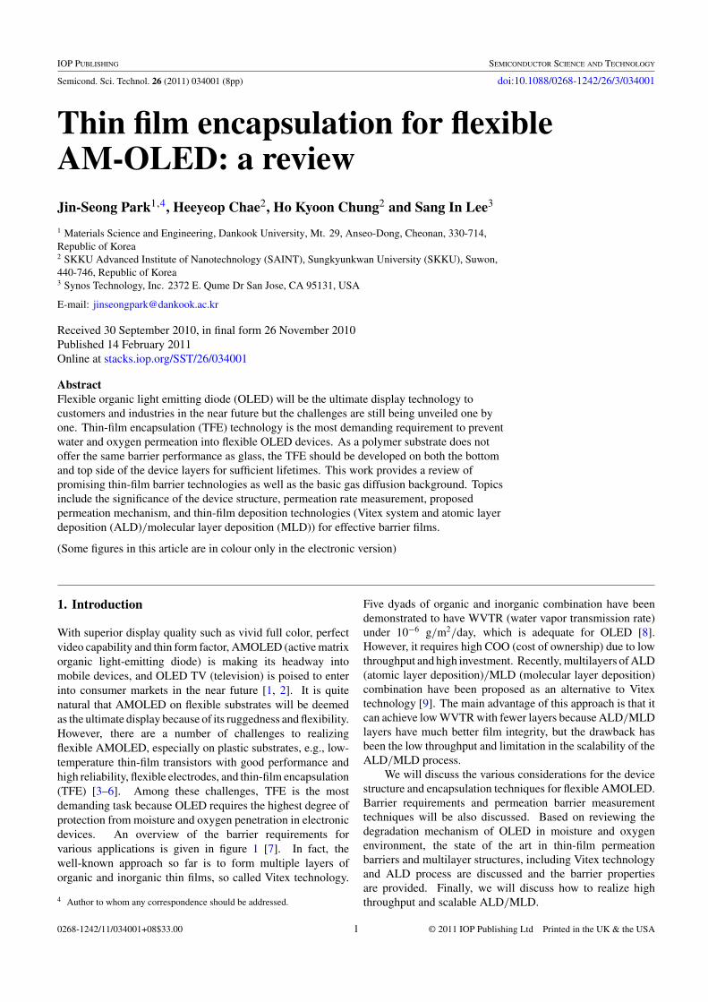
With superior display quality such as vivid full color, perfectvideo capability and thin form factor, AMOLED (active matrixorganic light-emitting diode) is making its headway intomobile devices, and OLED TV (television) is poised to enterinto consumer markets in the near future [1, 2]. It is quitenatural that AMOLED on flexible substrates will be deemedas the ultimate display because of its ruggedness and flexibility.However, there are a number of challenges to realizingflexible AMOLED, especially on plastic substrates, e.g., low-temperature thin-film transistors with good performance andhigh reliability, flexible electrodes, and thin-film encapsulation(TFE) [3–6]. Among these challenges, TFE is the mostdemanding task because OLED requires the highest degree ofprotection from moisture and oxygen penetration in electronicdevices. An overview of the barrier requirements forvarious applications is given in figure 1 [7]. In fact, thewell-known approach so far is to form multiple layers oforganic and inorganic thin films, so called Vitex technology.
4 Author to whom any correspondence should be addressed.
Five dyads of organic and inorganic combination have beendemonstrated to have WVTR (water vapor transmission rate)under 10−6 g/m2/day, which is adequate for OLED [8].However, it requires high COO (cost of ownership) due to lowthroughput and high investment. Recently, multilayers of ALD(atomic layer deposition)/MLD (molecular layer deposition)combination have been proposed as an alternative to Vitextechnology [9]. The main advantage of this approach is that itcan achieve low WVTR with fewer layers because ALD/MLDlayers have much better film integrity, but the drawback hasbeen the low throughput and limitation in the scalability of theALD/MLD process.
We will discuss the various considerations for the devicestructure and encapsulation techniques for flexible AMOLED.Barrier requirements and permeation barrier measurementtechniques will be also discussed. Based on reviewing thedegradation mechanism of OLED in moisture and oxygenenvironment, the state of the art in thin-film permeationbarriers and multilayer structures, including Vitex technologyand ALD process are discussed and the barrier propertiesare provided. Finally, we will discuss how to realize highthroughput and scalable ALD/MLD.
0268-1242/11/034001+08$33.00 1 © 2011 IOP Publishing Ltd Printed in the UK & the USA
Semicond. Sci. Technol. 26 (2011) 034001 J-S Park et al
Figure 1. Barrier requirements for different applications.
(a)
(b)
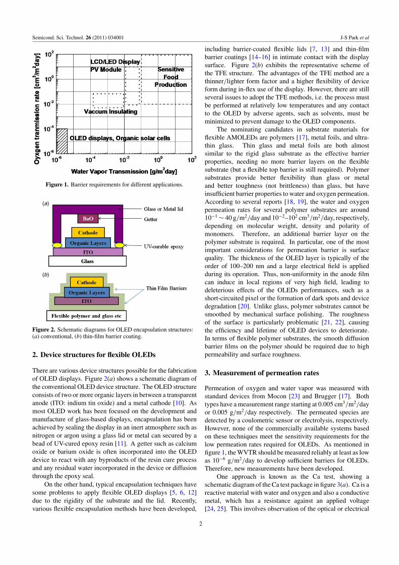
Figure 2. Schematic diagrams for OLED encapsulation structures:(a) conventional, (b) thin-film barrier coating.
2. Device structures for flexible OLEDs
There are various device structures possible for the fabricationof OLED displays. Figure 2(a) shows a schematic diagram ofthe conventional OLED device structure. The OLED structureconsists of two or more organic layers in between a transparentanode (ITO: indium tin oxide) and a metal cathode [10]. Asmost OLED work has been focused on the development andmanufacture of glass-based displays, encapsulation has beenachieved by sealing the display in an inert atmosphere such asnitrogen or argon using a glass lid or metal can secured by abead of UV-cured epoxy resin [11]. A getter such as calciumoxide or barium oxide is often incorporated into the OLEDdevice to react with any byproducts of the resin cure processand any residual water incorporated in the device or diffusionthrough the epoxy seal.
On the other hand, typical encapsulation techniques havesome problems to apply flexible OLED displays [5, 6, 12]due to the rigidity of the substrate and the lid. Recently,various flexible encapsulation methods have been developed,
including barrier-coated flexible lids [7, 13] and thin-filmbarrier coatings [14–16] in intimate contact with the displaysurface. Figure 2(b) exhibits the representative scheme ofthe TFE structure. The advantages of the TFE method are athinner/lighter form factor and a higher flexibility of deviceform during in-flex use of the display. However, there are stillseveral issues to adopt the TFE methods, i.e. the process mustbe performed at relatively low temperatures and any contactto the OLED by adverse agents, such as solvents, must beminimized to prevent damage to the OLED components.
The nominating candidates in substrate materials forflexible AMOLEDs are polymers [17], metal foils, and ultra-thin glass. Thin glass and metal foils are both almostsimilar to the rigid glass substrate as the effective barrierproperties, needing no more barrier layers on the flexiblesubstrate (but a flexible top barrier is still required). Polymersubstrates provide better flexibility than glass or metaland better toughness (not brittleness) than glass, but haveinsufficient barrier properties to water and oxygen permeation.According to several reports [18, 19], the water and oxygenpermeation rates for several polymer substrates are around10−1 ∼ 40 g/m2/day and 10−2–102 cm3/m2/day, respectively,depending on molecular weight, density and polarity ofmonomers. Therefore, an additional barrier layer on thepolymer substrate is required. In particular, one of the mostimportant considerations for permeation barrier is surfacequality. The thickness of the OLED layer is typically of theorder of 100–200 nm and a large electrical field is appliedduring its operation. Thus, non-uniformity in the anode filmcan induce in local regions of very high field, leading todeleterious effects of the OLEDs performances, such as ashort-circuited pixel or the formation of dark spots and devicedegradation [20]. Unlike glass, polymer substrates cannot besmoothed by mechanical surface polishing. The roughnessof the surface is particularly problematic [21, 22], causingthe efficiency and lifetime of OLED devices to deteriorate.In terms of flexible polymer substrates, the smooth diffusionbarrier films on the polymer should be required due to highpermeability and surface roughness.
3. Measurement of permeation rates
Permeation of oxygen and water vapor was measured withstandard devices from Mocon [23] and Brugger [17]. Bothtypes have a measurement range starting at 0.005 cm3/m2/dayor 0.005 g/m2/day respectively. The permeated species aredetected by a coulometric sensor or electrolysis, respectively.However, none of the commercially available systems basedon these techniques meet the sensitivity requirements for thelow permeation rates required for OLEDs. As mentioned infigure 1, the WVTR should be measured reliably at least as lowas 10−6 g/m2/day to develop sufficient barriers for OLEDs.Therefore, new measurements have been developed.
One approach is known as the Ca test, showing aschematic diagram of the Ca test package in figure 3(a). Ca is areactive material with water and oxygen and also a conductivemetal, which has a resistance against an applied voltage[24, 25]. This involves observation of the optical or electrical
2
Semicond. Sci. Technol. 26 (2011) 034001 J-S Park et al
(a)
(b)
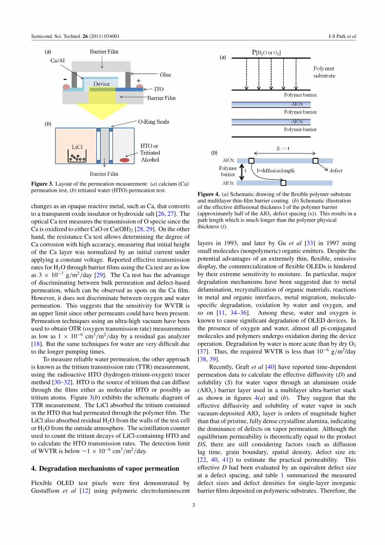
Figure 3. Layout of the permeation measurement: (a) calcium (Ca)permeation test, (b) tritiated water (HTO) permeation test.
changes as an opaque reactive metal, such as Ca, that convertsto a transparent oxide insulator or hydroxide salt [26, 27]. Theoptical Ca test measures the transmission of O specie since theCa is oxidized to either CaO or Ca(OH)2 [28, 29]. On the otherhand, the resistance Ca test allows determining the degree ofCa corrosion with high accuracy, measuring that initial heightof the Ca layer was normalized by an initial current underapplying a constant voltage. Reported effective transmissionrates for H2O through barrier films using the Ca test are as lowas 3 × 10⁻⁷ g/m2/day [29]. The Ca test has the advantageof discriminating between bulk permeation and defect-basedpermeation, which can be observed as spots on the Ca film.However, it does not discriminate between oxygen and waterpermeation. This suggests that the sensitivity for WVTR isan upper limit since other permeants could have been present.Permeation techniques using an ultra-high vacuum have beenused to obtain OTR (oxygen transmission rate) measurementsas low as 1 × 10⁻⁶ cm3/m2/day by a residual gas analyzer[18]. But the same techniques for water are very difficult dueto the longer pumping times.
To measure reliable water permeation, the other approachis known as the tritium transmission rate (TTR) measurement,using the radioactive HTO (hydrogen-tritium-oxygen) tracermethod [30–32]. HTO is the source of tritium that can diffusethrough the films either as molecular HTO or possibly astritium atoms. Figure 3(b) exhibits the schematic diagram ofTTR measurement. The LiCl absorbed the tritium containedin the HTO that had permeated through the polymer film. TheLiCl also absorbed residual H2O from the walls of the test cellor H2O from the outside atmosphere. The scintillation counterused to count the tritium decays of LiCl-containing HTO andto calculate the HTO transmission rates. The detection limitof WVTR is below ∼1 × 10⁻⁶ cm3/m2/day.
4. Degradation mechanisms of vapor permeation
Flexible OLED test pixels were first demonstrated byGustaffson et al [12] using polymeric electroluminescent
(b)
(a)
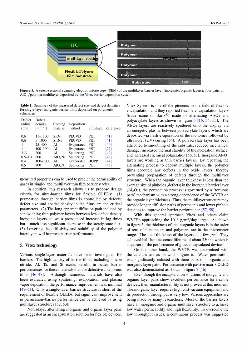
Figure 4. (a) Schematic drawing of the flexible polymer substrateand multilayer thin-film barrier coating. (b) Schematic illustrationof the effective diffusional thickness l of the polymer barrier(approximately half of the AlOx defect spacing (s)). This results in apath length which is much longer than the polymer physicalthickness (t).
layers in 1993, and later by Gu et al [33] in 1997 usingsmall molecules (nonpolymeric) organic emitters. Despite thepotential advantages of an extremely thin, flexible, emissivedisplay, the commercialization of flexible OLEDs is hinderedby their extreme sensitivity to moisture. In particular, majordegradation mechanisms have been suggested due to metaldelamination, recrystallization of organic materials, reactionsin metal and organic interfaces, metal migration, molecule-specific degradation, oxidation by water and oxygen, andso on [11, 34–36]. Among these, water and oxygen isknown to cause significant degradation of OLED devices. Inthe presence of oxygen and water, almost all pi-conjugatedmolecules and polymers undergo oxidation during the deviceoperation. Degradation by water is more acute than by dry O2
[37]. Thus, the required WVTR is less than 10−6 g/m2/day[38, 39].
Recently, Graft et al [40] have reported time-dependentpermeation data to calculate the effective diffusivity (D) andsolubility (S) for water vapor through an aluminum oxide(AlOx) barrier layer used in a multilayer ultra-barrier stackas shown in figures 4(a) and (b). They suggest that theeffective diffusivity and solubility of water vapor in suchvacuum-deposited AlOx layer is orders of magnitude higherthan that of pristine, fully dense crystalline alumina, indicatingthe dominance of defects on vapor permeation. Although theequilibrium permeability is theoretically equal to the productDS, there are still considering factors (such as diffusionlag time, grain boundary, spatial density, defect size etc[22, 40, 41]) to estimate the practical permeability. Thiseffective D had been evaluated by an equivalent defect sizeat a defect spacing, and table 1 summarized the measureddefect sizes and defect densities for single-layer inorganicbarrier films deposited on polymeric substrates. Therefore, the
3
Semicond. Sci. Technol. 26 (2011) 034001 J-S Park et al
Figure 5. A cross-sectional scanning electron microscopy (SEM) of the multilayer barrier layer (inorganic/organic layers): four pairs ofAlOx/polymer multilayer deposited by the Vitex barrier deposition system.
Table 1. Summary of the measured defect size and defect densitiesfor single-layer inorganic barrier films deposited on polymericsubstrates.
Defect Defectradius density Coating Deposition(mm) (mm−2) material method Substrate Reference
0.6 11–1100 SiO2 PECVD PET [41]0.6 5–1000 Si3N4 PECVD PET [41]1 25–400 Al Evaporated PET [40]1 100–300 Al Evaporated PET [22]2–3 200 Al Sputtering PET [42]0.5–1.4 600 AlOxNy Sputtering PET [43]0.4 100–1000 Al Evaporated BOPP [44]0.5 700 AlOxNy Sputtering PET [45]
measured properties can be used to predict the permeability ofgases in single- and multilayer thin film barrier stacks.
In addition, this research allows us to propose designcriteria for ultra-barrier films for flexible OLEDs: (1)permeation through barrier films is controlled by defects;defect size and spatial density in the films are the criticalparameters. (2) The long apparent diffusion path induced bysandwiching thin polymer layers between low defect densityinorganic layers causes a pronounced increase in lag timesbut a much less significant decrease in the steady-state flux.(3) Lowering the diffusivity and solubility of the polymerinterlayers will improve barrier performance.
5. Vitex technology
Various single-layer materials have been investigated forbarriers. The high density of barrier films, including siliconnitride, Al, Ta, and Si oxide, results in better barrierperformances for these materials than for defective and porousfilms [46–48]. Although numerous materials have alsobeen evaluated using sputtering, evaporation, and plasmavapor deposition, the performance improvement was minimal[49–51]. Only a single-layer barrier structure is short of therequirement of flexible OLEDs, but significant improvementin permeation–barrier performance can be achieved by usingmultilayer structures [52, 53].
Nowadays, alternating inorganic and organic layer pairsare suggested as an encapsulation solution for flexible devices.
Vitex System is one of the pioneers in the field of flexibleencapsulation and they reported flexible encapsulation layers(trade name of Barix R©) made of alternating Al2O3 andpolyacrylate layers as shown in figure 5 [16, 54, 55]. TheAl2O3 layers are reactively sputtered onto the display viaan energetic plasma between polyacrylate layers, which aredeposited via flash evaporation of the monomer followed byultraviolet (UV) curing [54]. A polyacrylate layer has beenattributed to smoothing of the substrate, reduced mechanicaldamage, increased thermal stability of the nucleation surface,and increased chemical polarization [56, 57]. Inorganic Al2O3
layers are working as thin barrier layers. By repeating thealternating process to deposit multiple layers, the polymerfilms decouple any defects in the oxide layers, therebypreventing propagation of defects through the multilayerstructure. When the organic layer thickness is less than theaverage size of pinholes (defects) in the inorganic barrier layer(Al2O3), the permeation process is governed by a ‘tortuouspath’ mechanism with a strong dependence of the WVTR onthe organic layer thickness. Thus, the multilayer structure mayprovide longer diffusion paths of permeants and lower pinholedensities to improve the barrier performance [57, 58].
With this general approach Vitex and others claimWVTRs approaching the 10−6 g/m2/day target. As shownin figure 5, the thickness of the inorganic layers is in the orderof tens of nanometers and polymers are in the micrometerrange. The total thickness of the layers is a few μm. Theyachieved half-luminescence lifetime of about 2500 h which isa quarter of the performance of glass encapsulated devices.
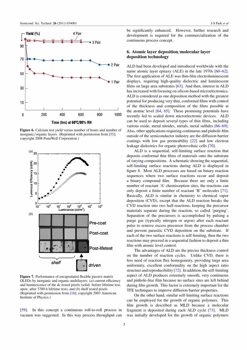
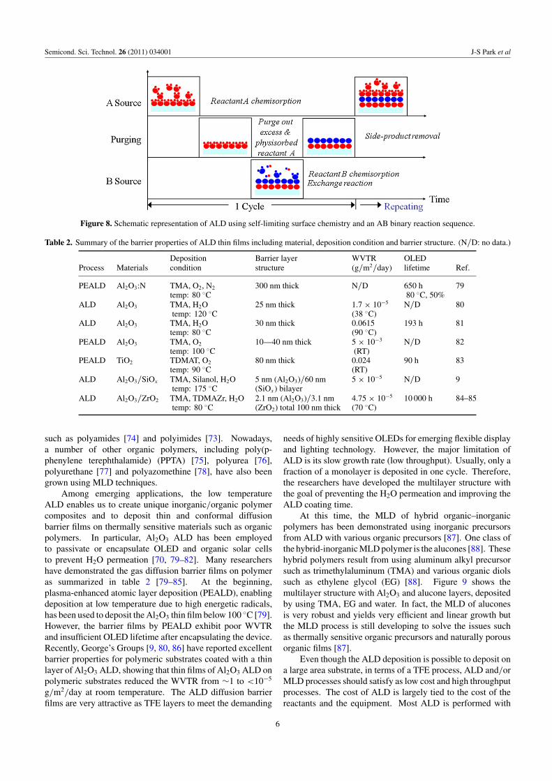
On the other hand, the WVTR was determined withthe calcium test as shown in figure 6. Water permeationwas significantly reduced with three pairs of inorganic andinorganic layer pairs. Performance with passive matrix OLEDwas also demonstrated as shown in figure 7 [16].
Even though the encapsulation solutions of inorganic andorganic layer pairs show excellent performance for flexibledevices, their manufacturability is not proven at this moment.The inorganic layer requires high cost vacuum equipment andits production throughput is very low. Various approaches arebeing made by many researchers. Most of the barrier layershave an inorganic and organic multilayer structure to achievelow water permeability and high flexibility. To overcome thelow throughput issues, a continuous process was suggested
4
Semicond. Sci. Technol. 26 (2011) 034001 J-S Park et al
Figure 6. Calcium test yield versus number of hours and number ofinorganic/organic layers. (Reprinted with permission from [55];copyright 2008 PennWell Corporation.)
(a)
(b)
Figure 7. Performance of encapsulated flexible passive matrixOLEDs by inorganic and organic multilayers: (a) current efficiencyand luminescence of the dc tested pixels (solid: before lifetime test,open: after 3700 h lifetime test), and (b) shelf tested pixels(Reprinted with permission from [16]; copyright 2003 AmericanInstitute of Physics.)
[59]. In this concept a continuous roll-to-roll process invacuum was suggested. In this way process throughput can
be significantly enhanced. However, further research anddevelopment is required for the commercialization of thecontinuous process concept.
6. Atomic layer deposition/molecular layerdeposition technology
ALD had been developed and introduced worldwide with thename atomic layer epitaxy (ALE) in the late 1970s [60–62].The first application of ALE was thin-film electroluminescentdisplays, requiring high-quality dielectric and luminescentfilms on large area substrates [63]. And then, interest in ALDhas increased with focusing on silicon-based microelectronics.ALD is considered as one deposition method with the greatestpotential for producing very thin, conformal films with controlof the thickness and composition of the films possible atthe atomic level [64, 65]. These promising potentials haverecently led to scaled down microelectronic devices. ALDcan be used to deposit several types of thin films, includingvarious oxide, metal nitrides, metals, metal sulfides [66–69].Also, other applications requiring continuous and pinhole-filmoutside of the semiconductor industry are the diffusion barriercoatings with low gas permeability [22] and low electronleakage dielectrics for organic photovoltaic cells [70].
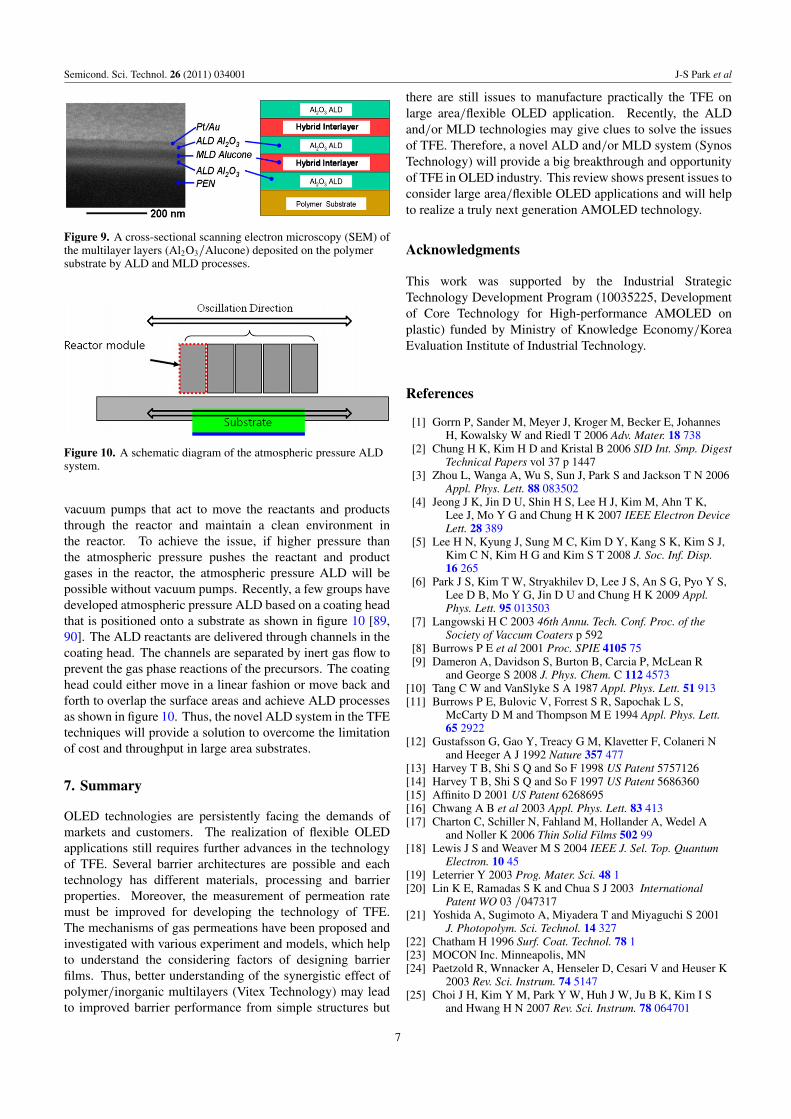
ALD is a sequential, self-limiting surface reaction thatdeposits conformal thin films of materials onto the substrateof varying compositions. A schematic showing the sequential,self-limiting surface reactions during ALD is displayed infigure 8. Most ALD processes are based on binary reactionsequences where two surface reactions occur and deposita binary compound film. Because there are only a finitenumber of reactant ‘A’ chemisorption sites, the reactions canonly deposit a finite number of reactant ‘B’ molecules [71].Basically, ALD is similar in chemistry to chemical vapordeposition (CVD), except that the ALD reaction breaks theCVD reaction into two half-reactions, keeping the precursormaterials separate during the reaction, so called ‘purging’.Separation of the precursors is accomplished by pulsing apurge gas (typically nitrogen or argon) after each reactantpulse to remove excess precursor from the process chamberand prevent parasitic CVD deposition on the substrate. Ifeach of the two surface reactions is self-limiting, then the tworeactions may proceed in a sequential fashion to deposit a thinfilm with atomic level control.
The advantages of ALD are the precise thickness controlon the number of reaction cycles. Unlike CVD, there isless need of reaction flux homogeneity, providing large areauniformity, excellent conformality on the high aspect ratiostructure and reproducibility [72]. In addition, the self-limitingaspect of ALD produces extremely smooth, very continuousand pinhole-free film because no surface sites are left behindduring film growth. This factor is extremely important for theTFE techniques to improve diffusion barrier properties.
On the other hand, similar self-limiting surface reactionscan be employed for the growth of organic polymers. Thisfilm growth is described as MLD because a molecularfragment is deposited during each ALD cycle [73]. MLDwas initially developed for the growth of organic polymers
5
Semicond. Sci. Technol. 26 (2011) 034001 J-S Park et al
Figure 8. Schematic representation of ALD using self-limiting surface chemistry and an AB binary reaction sequence.
Table 2. Summary of the barrier properties of ALD thin films including material, deposition condition and barrier structure. (N/D: no data.)
Deposition Barrier layer WVTR OLEDProcess Materials condition structure (g/m2/day) lifetime Ref.
PEALD Al2O3:N TMA, O2, N2 300 nm thick N/D 650 h 79temp: 80 ◦C 80 ◦C, 50%
ALD Al2O3 TMA, H2O 25 nm thick 1.7 × 10⁻⁵ N/D 80temp: 120 ◦C (38 ◦C)
ALD Al2O3 TMA, H2O 30 nm thick 0.0615 193 h 81temp: 80 ◦C (90 ◦C)
PEALD Al2O3 TMA, O2 10—40 nm thick 5 × 10⁻³ N/D 82temp: 100 ◦C (RT)
PEALD TiO2 TDMAT, O2 80 nm thick 0.024 90 h 83temp: 90 ◦C (RT)
ALD Al2O3/SiOx TMA, Silanol, H2O 5 nm (Al2O3)/60 nm 5 × 10⁻⁵ N/D 9temp: 175 ◦C (SiOx) bilayer
ALD Al2O3/ZrO2 TMA, TDMAZr, H2O 2.1 nm (Al2O3)/3.1 nm 4.75 × 10⁻⁵ 10 000 h 84–85temp: 80 ◦C (ZrO2) total 100 nm thick (70 ◦C)
such as polyamides [74] and polyimides [73]. Nowadays,a number of other organic polymers, including poly(p-phenylene terephthalamide) (PPTA) [75], polyurea [76],polyurethane [77] and polyazomethine [78], have also beengrown using MLD techniques.
Among emerging applications, the low temperatureALD enables us to create unique inorganic/organic polymercomposites and to deposit thin and conformal diffusionbarrier films on thermally sensitive materials such as organicpolymers. In particular, Al2O3 ALD has been employedto passivate or encapsulate OLED and organic solar cellsto prevent H2O permeation [70, 79–82]. Many researchershave demonstrated the gas diffusion barrier films on polymeras summarized in table 2 [79–85]. At the beginning,plasma-enhanced atomic layer deposition (PEALD), enablingdeposition at low temperature due to high energetic radicals,has been used to deposit the Al2O3 thin film below 100 ◦C [79].However, the barrier films by PEALD exhibit poor WVTRand insufficient OLED lifetime after encapsulating the device.Recently, George’s Groups [9, 80, 86] have reported excellentbarrier properties for polymeric substrates coated with a thinlayer of Al2O3 ALD, showing that thin films of Al2O3 ALD onpolymeric substrates reduced the WVTR from ∼1 to <10−5
g/m2/day at room temperature. The ALD diffusion barrierfilms are very attractive as TFE layers to meet the demanding
needs of highly sensitive OLEDs for emerging flexible displayand lighting technology. However, the major limitation ofALD is its slow growth rate (low throughput). Usually, only afraction of a monolayer is deposited in one cycle. Therefore,the researchers have developed the multilayer structure withthe goal of preventing the H2O permeation and improving theALD coating time.
At this time, the MLD of hybrid organic–inorganicpolymers has been demonstrated using inorganic precursorsfrom ALD with various organic precursors [87]. One class ofthe hybrid-inorganic MLD polymer is the alucones [88]. Thesehybrid polymers result from using aluminum alkyl precursorsuch as trimethylaluminum (TMA) and various organic diolssuch as ethylene glycol (EG) [88]. Figure 9 shows themultilayer structure with Al2O3 and alucone layers, depositedby using TMA, EG and water. In fact, the MLD of aluconesis very robust and yields very efficient and linear growth butthe MLD process is still developing to solve the issues suchas thermally sensitive organic precursors and naturally porousorganic films [87].
Even though the ALD deposition is possible to deposit ona large area substrate, in terms of a TFE process, ALD and/orMLD processes should satisfy as low cost and high throughputprocesses. The cost of ALD is largely tied to the cost of thereactants and the equipment. Most ALD is performed with
6
Semicond. Sci. Technol. 26 (2011) 034001 J-S Park et al
Figure 9. A cross-sectional scanning electron microscopy (SEM) ofthe multilayer layers (Al2O3/Alucone) deposited on the polymersubstrate by ALD and MLD processes.
Figure 10. A schematic diagram of the atmospheric pressure ALDsystem.
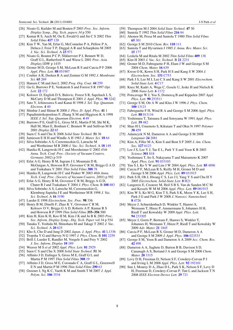
vacuum pumps that act to move the reactants and productsthrough the reactor and maintain a clean environment inthe reactor. To achieve the issue, if higher pressure thanthe atmospheric pressure pushes the reactant and productgases in the reactor, the atmospheric pressure ALD will bepossible without vacuum pumps. Recently, a few groups havedeveloped atmospheric pressure ALD based on a coating headthat is positioned onto a substrate as shown in figure 10 [89,90]. The ALD reactants are delivered through channels in thecoating head. The channels are separated by inert gas flow toprevent the gas phase reactions of the precursors. The coatinghead could either move in a linear fashion or move back andforth to overlap the surface areas and achieve ALD processesas shown in figure 10. Thus, the novel ALD system in the TFEtechniques will provide a solution to overcome the limitationof cost and throughput in large area substrates.
7. Summary
OLED technologies are persistently facing the demands ofmarkets and customers. The realization of flexible OLEDapplications still requires further advances in the technologyof TFE. Several barrier architectures are possible and eachtechnology has different materials, processing and barrierproperties. Moreover, the measurement of permeation ratemust be improved for developing the technology of TFE.The mechanisms of gas permeations have been proposed andinvestigated with various experiment and models, which helpto understand the considering factors of designing barrierfilms. Thus, better understanding of the synergistic effect ofpolymer/inorganic multilayers (Vitex Technology) may leadto improved barrier performance from simple structures but
there are still issues to manufacture practically the TFE onlarge area/flexible OLED application. Recently, the ALDand/or MLD technologies may give clues to solve the issuesof TFE. Therefore, a novel ALD and/or MLD system (SynosTechnology) will provide a big breakthrough and opportunityof TFE in OLED industry. This review shows present issues toconsider large area/flexible OLED applications and will helpto realize a truly next generation AMOLED technology.
Acknowledgments
This work was supported by the Industrial StrategicTechnology Development Program (10035225, Developmentof Core Technology for High-performance AMOLED onplastic) funded by Ministry of Knowledge Economy/KoreaEvaluation Institute of Industrial Technology.
References
[1] Gorrn P, Sander M, Meyer J, Kroger M, Becker E, JohannesH, Kowalsky W and Riedl T 2006 Adv. Mater. 18 738
[2] Chung H K, Kim H D and Kristal B 2006 SID Int. Smp. DigestTechnical Papers vol 37 p 1447
[3] Zhou L, Wanga A, Wu S, Sun J, Park S and Jackson T N 2006Appl. Phys. Lett. 88 083502
[4] Jeong J K, Jin D U, Shin H S, Lee H J, Kim M, Ahn T K,Lee J, Mo Y G and Chung H K 2007 IEEE Electron DeviceLett. 28 389
[5] Lee H N, Kyung J, Sung M C, Kim D Y, Kang S K, Kim S J,Kim C N, Kim H G and Kim S T 2008 J. Soc. Inf. Disp.16 265
[6] Park J S, Kim T W, Stryakhilev D, Lee J S, An S G, Pyo Y S,Lee D B, Mo Y G, Jin D U and Chung H K 2009 Appl.Phys. Lett. 95 013503
[7] Langowski H C 2003 46th Annu. Tech. Conf. Proc. of theSociety of Vaccum Coaters p 592
[8] Burrows P E et al 2001 Proc. SPIE 4105 75[9] Dameron A, Davidson S, Burton B, Carcia P, McLean R
and George S 2008 J. Phys. Chem. C 112 4573[10] Tang C W and VanSlyke S A 1987 Appl. Phys. Lett. 51 913[11] Burrows P E, Bulovic V, Forrest S R, Sapochak L S,
McCarty D M and Thompson M E 1994 Appl. Phys. Lett.65 2922
[12] Gustafsson G, Gao Y, Treacy G M, Klavetter F, Colaneri Nand Heeger A J 1992 Nature 357 477
[13] Harvey T B, Shi S Q and So F 1998 US Patent 5757126[14] Harvey T B, Shi S Q and So F 1997 US Patent 5686360[15] Affinito D 2001 US Patent 6268695[16] Chwang A B et al 2003 Appl. Phys. Lett. 83 413[17] Charton C, Schiller N, Fahland M, Hollander A, Wedel A
and Noller K 2006 Thin Solid Films 502 99[18] Lewis J S and Weaver M S 2004 IEEE J. Sel. Top. Quantum
Electron. 10 45[19] Leterrier Y 2003 Prog. Mater. Sci. 48 1[20] Lin K E, Ramadas S K and Chua S J 2003 International
Patent WO 03 /047317[21] Yoshida A, Sugimoto A, Miyadera T and Miyaguchi S 2001
J. Photopolym. Sci. Technol. 14 327[22] Chatham H 1996 Surf. Coat. Technol. 78 1[23] MOCON Inc. Minneapolis, MN[24] Paetzold R, Wnnacker A, Henseler D, Cesari V and Heuser K
2003 Rev. Sci. Instrum. 74 5147[25] Choi J H, Kim Y M, Park Y W, Huh J W, Ju B K, Kim I S
and Hwang H N 2007 Rev. Sci. Instrum. 78 064701
7
Semicond. Sci. Technol. 26 (2011) 034001 J-S Park et al
[26] Nisato G, Kuilder M and Bouten P 2003 Proc. Soc. Inform.Display Symp., Dig. Tech. papers 34 p 550
[27] Kumar R S, Auch M, Ou E, Ewald G and Jin C S 2002 ThinSolid Films 417 120
[28] Kim T W, Yan M, Erlat G, McConnelee P A, Pellow P A,Deluca J, Feist T P, Duggal A R and Schaepkens M 2005J. Vac. Sci. Technol. A 23 971
[29] Nisato G, Bouten P C P, Slikkerveer P J, Bennett W D,Graff G L, Rutherford N and Wiese L 2001 Proc. AsiaDisplay/IDW p 1435
[30] Groner M D, George S M, McLean R S and Carcia P F 2006Appl. Phys. Lett. 88 051907
[31] Coulter A R, Deeken R A and Zentner G M 1992 J. MembraneSci. 65 269
[32] Hansen C M and Just L 2002 Prog. Org. Coat. 44 259[33] Gu G, Burrows P E, Venkatesh S and Forrest S R 1997 Opt.
Lett. 22 172[34] Kolosov D, English D S, Bulovic, Forest S R, Sapchack L S,
McCarty D M and Thompson E 2001 J. Appl. Phys. 90 3242[35] Sato Y, Ichinosawa S and Kanai H 1998 J. Sel. Top. Quantum
Electron. 4 40[36] Shinbar J and Shinar R 2008 J. Phys. D: Appl. Phys. 41 1[37] Papadimitrikopoulous F, Zhang X M and Higgison K A 1998
IEEE J. Sel. Top. Quantum Electron. 4 49[38] Burrows P E, Graff G L, Gross M E, Martin P M, Shi M K,
Hall M, Mast E, Bonham C, Bennett W and Sullivan M B2001 Display 22 65
[39] Suen C S and Chu X 2008 Solid State Technol. 51 36[40] Jamieson E H H and Windle A H 1983 J. Mater. Sci. 18 64[41] Silva Sobrinho A S, Czeremuszkin G, Latrache M
and Wertheimer M R 2000 J. Vac. Sci. Technol. A 18 149[42] Hanika H, Langowski H C and Moosheimer U 2002 45th
Annu. Tech. Conf. Proc. (Society of Vacuum Coaters,Germany 2002) p 519
[43] Erlat A G, Henry B M, Ingram J J, Mountain D B,McGuigan A, Howson R P, Grovenor C R M, Briggs G A Dand Tsukahara Y 2001 Thin Solid Films 388 78
[44] Hanika H, Langowski H C and Peuker W 2003 46th Annu.Tech. Conf. Proc. (Society of Vacuum Coaters, 2003) p 592
[45] Erlat A G, Henry B M, Grovenor C R M, Briggs A G D,Chater R J and Tsukahara Y 2004 J. Phys. Chem. B 108 883
[46] Silva Sobrinho A S, Latreche M, Czeremuszkin G,Klemberg-Sapieha J E and Wertheimer M R 1998 J. Vac.Sci. Technol. A 16 3190
[47] Lueder E 1998 Electrochem. Soc. Proc. 98 336[48] Henry B M, Dinelli F, Zhao K Y, Grovenor C R M,
Kolosov O V, Briggs G A D, Roberts A P, Kumar R Sand Howson R P 1999 Thin Solid Films 355–356 500
[49] Kim H, Kim K H, Koo H M, Kim J K and Ju B K 2003 Proc.Soc. Inform. Display Symp., Dig. Tech. Paper vol 34 p 554
[50] Tanaka T, Yoshida M, Shinohara M and Takagi T 2002 J. Vac.Sci. Technol. A 20 625
[51] Kho S, Cho D and Jung D 2002 Japan. J. Appl. Phys. 41 L1336[52] Tropsha Y G and Harvey N G 1997 J. Phys. Chem. B 101 2259[53] Brill J, Lueder E, Randler M, Voegele S and Frey V 2002
J. Soc. Inform. Display 10 189[54] Weaver M S et al 2002 Appl. Phys. Lett. 81 2929[55] Suen C S and Chu X 2008 Solid State Technol. 51 36[56] Affinito J D, Eufinger S, Gross M E, Graff G L and
Martin P M 1997 Thin Solid Films 308 19[57] Affinito J D, Gross M E, Coronado C A, Graff G L, Greenwell
E N and Martin P M 1996 Thin Solid Films 290 63[58] Greener J, Ng K C, Vaeth K M and Smith T M 2007 J. Appl.
Polym. Sci. 106 3534
[59] Thornpson M J 2004 Solid State Technol. 47 30[60] Suntola T 1992 Thin Solid Films 216 84[61] Ahonen M, Pessa M and Suntola T 1980 Thin Solid Films
65 301[62] George S M 2010 Chem. Rev. 110 111[63] Suntola T and Hyvarinen J 1985 J. Annu. Rev. Mater. Sci.
15 177[64] Leskela M and Ritala M 2002 Thin Solid Films 409 138[65] Kim H 2003 J. Vac. Sci. Technol. B 21 2231[66] Groner M D, Fabreguette F H, Elam J W and George S M
2004 Chem. Mater. 16 639[67] Kwon O K, Kown S H, Park H S and Kang S W 2004 J.
Electrochem. Soc. 151 C753[68] Park J S, Lee M J, Lee C S and Kang S W 2001 Elecrochem.
Solid-State Lett. 4 C17[69] Knez M, Kadri A, Wege C, Gosele U, Jeske H and Nielsch K
2006 Nano Lett. 6 1172[70] Potscavage W J, Yoo S, Domercq B and Kippelen 2007 Appl.
Phys. Lett. 90 253511[71] George S M, Ott A W and Klus J W 1996 J. Phys. Chem.
100 13121[72] Fabreguette F H, Wind R A and George S M 2006 Appl. Phys.
Lett. 88 013116[73] Yoshimura T, Tatsuura S and Sotoyama W 1991 Appl. Phys.
Lett. 59 482[74] Shao H I, Umemoto S, Kikutani T and Okui N 1997 Polymer
38 459[75] Adamcyzk N M, Dameron A A and George S M 2008
Langmuir 24 2081[76] Kim A, Filler M A, Kim S and Bent S F 2005 J. Am. Chem.
Soc. 127 6123[77] Lee J S, Lee Y J, Tae E L, Park Y S and Yoon K B 2003
Science 301 818[78] Yoshimura T, Ito S, Nakayama T and Matsumoto K 2007
Appl. Phys. Lett. 91 033103[79] Yun S J, Ko Y W and Lim J W 2004 Appl. Phys. Lett. 85 4896[80] Carcia P F, McLean R S, Reilly M H, Groner M D and
George S M 2006 Appl. Phys. Lett. 89 031915[81] Park S H, Oh J, Hwang C S, Lee J I, Yang Y S and Chu H Y
2005 Electrochem. Solid-State Lett. 8 H21[82] Langereis E, Creatore M, Heil S B S, Van de Sanden M C M
and Kessels W M M 2006 Appl. Phys. Lett. 89 081915[83] Kim W S, Ko M G, Kim T S, Park S K, Moon Y K, Lee S H,
Park J G and Park J W 2008 J. Nanosci. Nanotechnol.8 4726
[84] Meyer J, Schneidenbach D, Winkler T, Hamwi S,Weimann T, Hinze P, Ammermann S, Johannes H H,Riedl T and Kowalsky W 2009 Appl. Phys. Lett.94 233305
[85] Meyer J, Gorrn P, Bertram F, Hamwi S, Winkler T,Johannes H, Weimann T, Hinze P, Riedl T and Kowalsky W2009 Adv. Mater. 21 1845
[86] Carcia P F, McLean R S, Groner M D, Dameron A Aand George S M 2009 J. Appl. Phys. 106 023533
[87] George S M, Yoon B and Dameron A A 2009 Acc. Chem. Res.42 498
[88] Dameron A A, Saghete D, Burton B B, Davison S D,Cananagh A S, Bertand J A and George S M 2008 Chem.Mater. 20 3315
[89] Levy D H, Freeman D, Nelson S F, Cowdery-Corvan P Jand Irving L M 2008 Appl. Phys. Lett. 92 192101
[90] Sun J, Mourey D A, Zhao D L, Park S K, Nelson S F, Levy DH, Freeman D, Cowdery-Corvan P, Tutt L and Jackson T N2008 IEEE Electron Device Lett. 29 721
8