Embed Size (px)
Citation preview

The Voltage-Controlled Compensation Ramp: A Waveshaping Technique for
Power Factor Correctors
Javier Sebastián, Diego González Lamar, Manuel Arias, Miguel Rodríguez and Arturo Fernández
Universidad de Oviedo. Departamento de Ingeniería Eléctrica, Electrónica, de Computadores y de Sistemas. Grupo de
Sistemas Electrónicos de Alimentación (SEA)
Edificio Departamental nº 3. Campus Universitario de Viesques. 33204 Gijón. SPAIN
Phone: +34 985 18 20 85; e-mail: [email protected]
.
Abstract- This paper deals with a new control method for Power Factor Correctors. Control is carried out by a
standard IC controller for peak current-mode dc-dc converters, with only an additional compensation ramp generator
and peak detector. Neither an analog multiplier nor an input voltage sensor is needed to achieve quasi-sinusoidal line
waveforms, which makes this method very attractive. The method is similar to the One-Cycle Control method, but can be
very easily adapted for use with topologies different to the boost converter, i.e. flyback, buck-boost, SEPIC, Cuk and zeta
topologies. Moreover, as the line current is cycle-by-cycle controlled, the resulting input current feedback loop is
extremely fast, thus allowing the use of this type of control with high frequency lines.
This paper has been presented at the 2008 IEEE Applied Power Electronics Conference (APEC) in Austin, Texas, on February
27th with the same title and the same authors.
Corresponding Author Information:
Javier Sebastián
Universidad de Oviedo, Grupo de Sistemas Electrónicos de Alimentación (SEA)
Edificio 3, Campus de Viesques s/n, 33204 Gijón, SPAIN
Phone: +34 985 18 20 85
Fax: +34 985 18 21 38
e-mail: [email protected]

The Voltage-Controlled Compensation Ramp: A Waveshaping Technique for Power Factor Correctors
Abstract- This paper deals with a new control method for Power Factor Correctors. Control is carried out
by a standard IC controller for peak current-mode dc-dc converters, with only an additional compensation
ramp generator and peak detector. Neither an analog multiplier nor an input voltage sensor is needed to
achieve quasi-sinusoidal line waveforms, which makes this method very attractive. The method is similar to
the One-Cycle Control method, but can be very easily adapted for use with topologies different to the boost
converter, i.e. flyback, buck-boost, SEPIC, Cuk and zeta topologies. Moreover, as the line current is cycle-by-
cycle controlled, the resulting input current feedback loop is extremely fast, thus allowing the use of this type
of control with high frequency lines.
I. INTRODUCTION
Power Factor Correctors (PFCs) are widely used as the first stage in many ac-dc power supply systems,
especially if the total power handled by the system is above 75 W. Among the methods proposed to control PFCs [1-
14, 17-19], the following three are the most popular:
A. Voltage-Follower Control [2-9]
A very simple solution providing an almost sinusoidal (in the case of the boost converter [3]) or completely
sinusoidal (in the case of the flyback family of converters [4-7]) line current waveform consists in designing the
topology to always operate in the Discontinuous Conduction Mode (DCM) [4-7, 15]. In this case, only one voltage
feedback loop (see Fig. 1a) is needed [2-9]. Since only one feedback loop is used to control the converter, and as any
conventional switching-mode power supply controller can be used for this purpose, the control circuitry is hence
extremely simple. Another advantage of this option is that the output diode does not exhibit reverse recovery
problems because it is not conducting any current when the transistor is turned on.
However, this option also has certain drawbacks. For example, the peak value of the current passing through
many components (transistor, diode, inductor, input and output filter capacitors, etc.) is about twice as high as in the
case of operating in Continuous Conduction Mode (CCM). Consequently, the conduction losses are clearly higher.
Even the switching losses when the transistor is turned off are higher than in the case of operating in CCM.

B. Analog-Multiplier based Control [1, 2]
The classical method for obtaining a perfectly sinusoidal line waveform consists in using a control strategy based
on two feedback loops, one input-current feedback loop and an output-voltage feedback loop. Furthermore, an
analog multiplier must be used in the control circuitry (see Fig. 1.b). This option means that the converter can work
in both modes of operation (DCM and CCM). By designing the converter to operate in CCM at heavy loads, the
current stress is clearly lower than in the case of operating in DCM at these loads. Therefore, efficiency is higher
using this option.
The main disadvantage of this option is the complexity of the control circuitry and its cost. Several controllers
can be used for this purpose, but they are not cheap, especially in comparison with standard controllers for
-PWM
Vref
+Line
Av
CB
vg
+
-
PFC(Power Stage
in DCM)
ilineOutput
Voltage feedback loop
-PWM
Vref
+Line
Av
CB
vg
+
-
PFC(Power Stage
in DCM)
ilineOutput
Voltage feedback loop
(a)
-
-
PWM
Vref
+Line
Av
CB
vg
+
-
PFC(Power Stage)
ilineOutput
Ai
Voltage feedback loop
Current feedback loop
-
-
PWMPWM
Vref
+Line
Av
CB
vg
+
-
PFC(Power Stage)
ilineOutput
Ai
Voltage feedback loop
Current feedback loop
-One-CycleController
Vref
+Line
CB
vg
+
-
PFC(Power Stage)iline
Output
Av
Voltage feedback loop
Current loop
-One-CycleControllerOne-CycleController
Vref
+Line
CB
vg
+
-
PFC(Power Stage)iline
Output
AvAv
Voltage feedback loop
Current loop
(b) (c)
Fig. 1: Three of the most popular methods for controlling PFCs. a) Voltage-Follower Control. b) Analog-Multiplier Based Control. c) One-
Cycle Control.

switching-mode power supplies. If the converter has to be a very low-cost one, the use of PFC controllers based on
an analog multiplier becomes relatively expensive. Finally, the available controllers based on this technique cannot
operate above 400 Hz due to their limited input-current error amplifier bandwidth, which means that this method is
unsuitable for use in the case of high-frequency lines (clearly above 400 Hz).
C. One-Cycle Control [18-22]
In the last years, some authors have proposed different low cost control strategies for PFCs operating in CCM
[16-22]. The objective of these control strategies is to simplify the existing control circuitry based on an analog
multiplier. This simplification makes sense in the case of relatively low-power and wide input voltage range
applications, as PFCs for many types of PC power supplies, electronic ballast and battery chargers in the range of
100-500 W. The One-Cycle Control (OCC) technique is a significant low cost strategy to control PFCs based on the
boost converter topology. It was introduced in [18] for any type of switching converter. This type of control is
proposed in [19] to be used in PFCs (see Fig. 1.c), where it is termed Linear Peak Current Mode Control (LPCMC).
In [20], the idea of OCC is generalized to obtain a general pulsewidth modulator, which is particularized in [21] to be
used in PFC applications. For the particular case of the boost PFC, this general pulsewidth modulator becomes the
same as the LPCMC [21], and it is called again OCC in [22]. It is quite simple because it does not need to use an
analog multiplier, in spite of being used in PFCs operating in CCM. Moreover, no input voltage sensing is needed
using OCC. As it has been mentioned, the implementation of this control method is quite simple in the case of PFCs
based on boost converters, because only one signal integrator is needed. It should be noted that the integrator time
constant must match the switching period [18, 19] for proper operation. In the case of PFCs based on converters
belonging to the flyback family (i.e. buck-boost, SEPIC, Cuk and zeta), either two matched integrators or a current
sensor with an integrator with reset must be used [20,21]. This fact makes this method less attractive in the case of
the flyback family of converters.
A new low-cost control strategy for wide PFCs is presented in this paper. This control strategy is called Voltage-
Controlled Compensation Ramp (VCCR) Control. It allows the use of conventional peak current-mode controllers
for switching-mode power supply to control wide input voltage range PFCs operating in CCM. Thus, both low-cost
(due to the controller used) and high efficiency (due to the CCM operation) are achieved. Moreover, input current is
cycle-by-cycle controlled. Therefore, the input current feedback loop is extremely fast, thereby allowing this type of
control to be used with relatively high frequency lines (clearly above 400Hz). It should be noted that the line
frequency used in the electrical power distribution system in aircrafts is 400 Hz and higher frequencies have been
under consideration. The price to pay for these advantages is the quality of the line waveform, which will be very
sinusoidal at full load, but will be less sinusoidal when the load decreases. However, this is not a major problem,
since regulations (especially IEC-1000-3-2, [23, 24]) must be met only at full load and due to the fact that the line
waveform maintains a very high Power Factor (PF) under all operating conditions.
The implementation of VCCR Control for the case of PFCs based on the boost converter is very similar to the
OCC implementation for the same PFC [22]. However, the VCCR control method avoids critical matching between
the integrator time constant and the switching period [20, 21, 22] and can be very easily modified for use with PFCs
based on the flyback family of converters.
II. COMPARISON BETWEEN OCC AND VCCR CONTROL
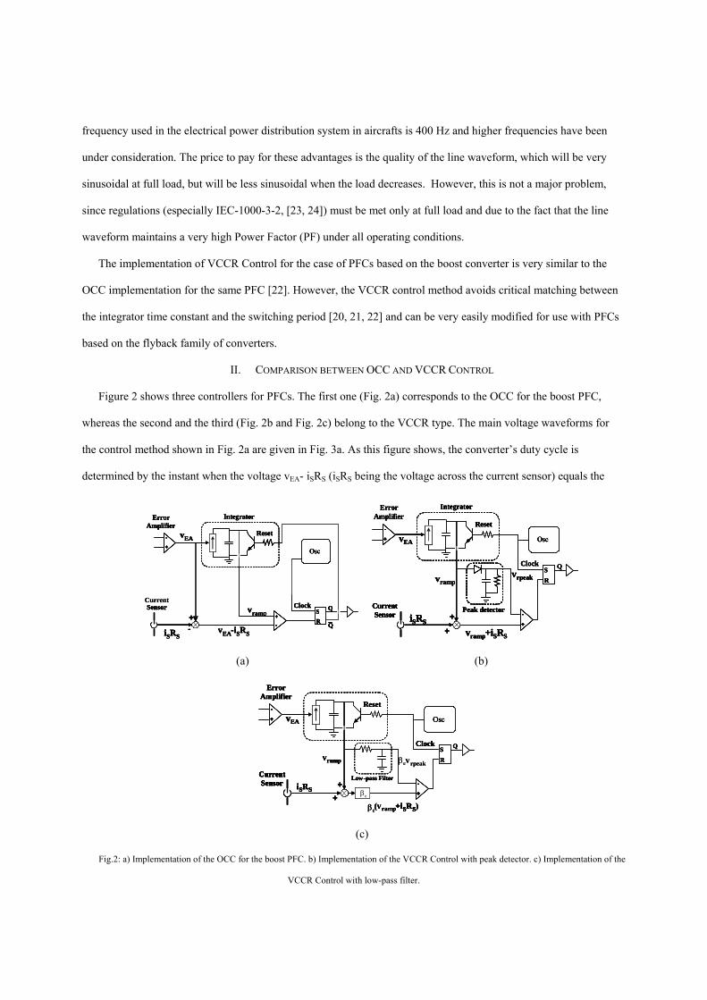
Figure 2 shows three controllers for PFCs. The first one (Fig. 2a) corresponds to the OCC for the boost PFC,
whereas the second and the third (Fig. 2b and Fig. 2c) belong to the VCCR type. The main voltage waveforms for
the control method shown in Fig. 2a are given in Fig. 3a. As this figure shows, the converter’s duty cycle is
determined by the instant when the voltage vEA- iSRS (iSRS being the voltage across the current sensor) equals the
Clock
Osc
RS Q
+
-
Q-
vEA
+
-
Reset
vramp
Error Amplifier
Sensor
iSRSvEA-iSRS
Integrator
+Clock
Osc
RS Q
+
-
+
-
QQ-
vEA
+
-
+
-
Reset
vramp
Error Amplifier
CurrentSensor
iSRSvEA-iSRS
Integrator
+Clock
Osc
RS Q
+
-
Q-
vEA
+
-
Reset
vramp
Error Amplifier
Sensor
iSRSvEA-iSRS
Integrator
+Clock
Osc
RS Q
+
-
+
-
QQ-
vEA
+
-
+
-
Reset
vramp
Error Amplifier
CurrentSensor
iSRSvEA-iSRS
Integrator
+
RS Q
+
-
vEA
+
-
vramp
Error Amplifier
vramp+iSRS
Clock
Osc
Reset
Integrator
CurrentSensor iSRS
Peak detector
vrpeak
++
RS Q
+
-
+
-
vEA
+
-
+
-
vramp
Error Amplifier
vramp+iSRS
Clock
Osc
Reset
Integrator
CurrentSensor iSRS
CurrentSensor iSRS
Peak detector
vrpeak
++
RS Q
+
-
vEA
+
-
vramp
Error Amplifier
vramp+iSRS
Clock
Osc
Reset
Integrator
CurrentSensor iSRS
Peak detector
vrpeak
++
RS Q
+
-
+
-
vEA
+
-
+
-
vramp
Error Amplifier
vramp+iSRS
Clock
Osc
Reset
Integrator
CurrentSensor iSRS
CurrentSensor iSRS
Peak detector
vrpeak
++
(a) (b)
R
S Q
+
-
vEA
+
-
vramp
Error Amplifier
Clock
Osc
Reset
CurrentSensor iSRS
Low-pass Filter
βev
0.5+
+
R
S Q
+
-
+
-
vEA
+
-
+
-
vramp
Error Amplifier
(v +iSRS)βe ramp+iSRS
Clock
Osc
Reset
CurrentSensor iSRS
CurrentSensor iSRS
Low-pass Filter
rpeak
0.5βe
++
R
S Q
+
-
vEA
+
-
vramp
Error Amplifier
Clock
Osc
Reset
CurrentSensor iSRS
Low-pass Filter
βev
0.5+
+
R
S Q
+
-
+
-
vEA
+
-
+
-
vramp
Error Amplifier
(v +iSRS)βe ramp+iSRS(v +iSRS)βe ramp+iSRS
Clock
Osc
Reset
CurrentSensor iSRS
CurrentSensor iSRS
Low-pass Filter
rpeak
0.5βe
++
(c)
Fig.2: a) Implementation of the OCC for the boost PFC. b) Implementation of the VCCR Control with peak detector. c) Implementation of the
VCCR Control with low-pass filter.

value of the integrator output at that instant [22]. For this method to operate properly, the time constant of the
integrator must be equal to the switching period TS. As a consequence of this, the peak value of the ramp, vrpeak, is
equal to the control signal, vEA.
On the other hand, the converter’s duty cycle in the circuit shown in Fig. 2b is determined by the instant when the
voltage vramp+iSRS equals the peak value of the ramp, vrpeak (see Fig. 3b). Therefore, no matching between the time
constant of the integrator and the switching period TS is needed. Two implementations are possible to determine
vrpeak. The first one is based on the use of a peak detector to calculate vrpeak (Fig. 2b). The second one is based on the
fact that the dc component of a compensation ramp waveform is always proportional to its peak value, βe being the
proportionality constant. In the case of a linear compensation ramp βe equals 0.5. Consequently, the converter’s duty
cycle can be obtained by using a very simple RC low-pass filter, as is shown in Fig. 2c.
In summary, OCC and VCCR Control are very similar methods. However, the main difference between them is
the way of determining the peak value of the ramp waveform, vrpeak. In the case of OCC, the time constant of the
integrator must be adjusted to obtain vrpeak = vEA, whereas VCCR Control obtains the value of vrpeak either by a peak
detector or by a low-pass filter, but with no any particular matching in the integrator time constant. It should be noted
that this matching is not a major problem if the integrator is based on an operational amplifier. However, if the
integrator is based on a general purpose PNP bipolar transistor in order to maintain the cost as low as possible, this
matching is very difficult because the integrator time constant depends on the transistor gain hFE, which can differ
from one transistor to another. Moreover, when OCC is implemented in an IC (like IR 1150) [22], this matching
TS
t
Driver signal
vEA-iSRS
t
dTS
vramp
vEA
vrampvrpeak
iSRS
t t
t
TS
t
Driver signal
dTS
iSRS+vramp
vrpeak
vramp
vrpeak
iSRS
t
TS
t
Driver signal
vEA-iSRS
t
dTS
vramp
vEA
vrampvrpeak
iSRS
t
TS
t
Driver signal
vEA-iSRS
t
dTS
vramp
vEA
vrampvrpeak
iSRS
t t
t
TS
t
Driver signal
dTS
iSRS+vramp
vrpeak
vramp
vrpeak
iSRS
tt
t
TS
t
Driver signal
dTS
iSRS+vramp
vrpeak
vramp
vrpeak
iSRS
t
(a) (b)
Fig.3: a) Main waveforms in Fig. 2a. b) Main waveforms in Fig. 2b.

process is achieved internally and the integrator capacitor is not externally accessible. This fact makes it impossible
to modify the integration process to adapt it to be used for other PFCs, as it will be described for VCCR Control in
Section V.
For conventional dc-dc converters, OCC has the advantage of faster response if vEA undergoes extremely fast
variations. However, this advantage disappears when controlling PFCs, since vEA undergoes slow variations due to
the bandwidth limitations of the output-voltage feedback loop [1,2]. This is due to the fact that a 10-20 Hz low-pass
filter is placed into the error amplifier of the voltage feedback loop to obtain a low distortion of the line current.
Hence, the use of either the peak detector or of the low-pass filter (see Fig 2b and Fig. 2c) in VCCR control, both
designed to operate according to the switching frequency (around 100 kHz), does not represent any appreciable
additional bandwidth limitation in comparison to the one due to the error amplifier. Moreover, the implementation of
VCCR Control has the advantage of being suitable for other type of compensation ramps, which will make it
possible to use this control method with PFCs based on other types of converters besides the boost converter.
III. INPUT CURRENT STATIC ANALYLIS OF THE BOOST PFC WITH OCC AND VCCR CONTROL
Figure 4.a shows a boost PFC with either OCC or VCCR Control. The control waveforms for this converter
operating in CCM are shown in Fig. 3. These waveforms can be synthesized in the waveforms given in Fig. 4b. If the
converter is operating in DCM, the main waveforms become the ones given in Fig. 4c. In both cases, the converter
duty cycle d is determined by the control signal vrpeak. The relationship between vEA and vrpeak is:
EAi0rpeak vkkv += , (1)
where k0 and ki are constant parameters (k0 is zero and ki is 1 in the case of OCC). From geometric relationships
in these waveforms, we can easily obtain:
S
rpeak2S R
d)(1vi
−= , (2)
where iS2 is the value of transistor current just before it stops conducting. The remaining equations needed to
study the converter operation depend on the conduction mode.

A. Operation in Continuous Conduction Mode (CCM)
In this case, Faraday’s law applied to both the transistor and the diode conduction periods yields:
d
iiLfv 1S2S
Sg−
= , (3)
d1
iiLfvV 1S2S
Sgo−
−=− , (4)
where iS1 is the value of transistor current when it starts conducting, fS is the switching frequency (fS=1/TS), vg is
the input voltage and VO is the output voltage. From (2)-(4), we can easily obtain:
S
rpeak
o
g2S R
v
V
vi ⋅= , (5)
⎥⎦
⎤⎢⎣
⎡ −−=
S
go
S
rpeak
o
g1S Lf
vV
R
v
V
vi . (6)
The value of the average inductor (and line) current igav is:
2
iii 1S2Sgav
+= , (7)
and from (5)-(7), we can obtain:
-OCC orVCCR
Controller
Vref
+Line
CB
vg
+
-
iline
Output
Av
Voltage feedback loop
Current loop
VO
+
-
ig
iS
iD
vEA
L
RS
-OCC orVCCR
Controller
Vref
+Line
CB
vg
+
-
iline
Output
Av
Voltage feedback loop
Current loop
VO
+
-
ig
iS
iD
vEA
L
-OCC orVCCR
Controller
Vref
+Line
CB
vg
+
-
iline
Output
Av
Voltage feedback loop
Current loop
VO
+
-
ig
iS
iD
vEA -OCC orVCCR
Controller
Vref
+Line
CB
vg
+
-
iline
Output
AvAv
Voltage feedback loop
Current loop
VO
+
-
ig
iS
iD
vEA
L
RS
iS1RS
vrpeak-vramp
tiSRS
iS2RS
vrpeak
TS
iS1
tdTS
igiS2
iS1RS
vrpeak-vramp
tiSRS
iS2RS
vrpeak
TS
iS1
tdTS
igiS2
t
TS
tdTS
vrpeak-vramp
iSRS
iS2RS
vrpeak
igiS2
d’TS
t
TS
tdTS
vrpeak-vramp
iSRS
iS2RS
vrpeak
igiS2
d’TS
(a) (b) (c)
Fig.4: a) Boost PFC with OCC or VCCR Control. b) Waveforms in CCM. c) Waveforms in DCM.

⎥⎦
⎤⎢⎣
⎡ −−=
S
go
S
rpeak
o
ggav Lf2
vV
R
v
V
vi . (8)
This last equation shows that if the product Lfs satisfies the relationship
rpeak
SgoS v
R
2
vVLf ⋅
−>> , (9)
then igav and vg will be proportional, performing ideal power factor correction.
B. Operation in Discontinuous Conduction Mode (DCM)
Figure 4.c shows the same waveforms as those shown in Fig. 4.b, though now with the converter operating in
DCM. In this case, iS1 is always zero and (3) and (4) become:
d
iLfv 2S
Sg = , (10)
d'
iLfvV 2S
Sgo =− . (11)
From (2) and (10), we can obtain:
Sg
rpeakSS
rpeak2S
Rv
vLf1
1
R
vi
+
⋅= . (12)
The value of igav is, in this case:
2
)d'(dii 2Sgav
+= , (13)
and from (10)-(13), we finally obtain:
2
S
g
S
rpeakSgo
og2
S
rpeakgav
Lf
v
R
v
1
Lf)v(V
Vv
R
v
2
1i
⎟⎟⎠
⎞⎜⎜⎝
⎛⎟⎟⎠
⎞⎜⎜⎝
⎛
+
⋅−
= . (14)
C. Boundary between both conduction modes
The value of iS1 is given by (6) in CCM, whereas it is equal to zero in DCM. Therefore, (6) must be equal to zero
just on the boundary between both modes, That is:

S
goSrpeak_crit Lf
vVRv
−= , (15)
where vrpeak_crit is the value of vrpeak that determines the boundary between modes. A dimensionless parameter K
will be used to study the boundaries between CCM and DCM:
gPS
rpeakS
VR
vLf2K = , (16)
where VgP is the peak value of the line voltage:
tsinωVv LgPg = . (17)
Moreover, we shall define another dimensionless parameter M as follows:
gPo VVM= . (18)
From (15)-(18), we can define the boundary value of K:
)tsinω2(MK Lcrit −= . (19)
Kcrit has different values depending on the line angle. Hence, its maximum and minimum values are, respectively:
M2K crit_max = , (20)
1)2(MKcrit_min −= . (21)
Therefore, three operation modes are possible: Always in CCM, if K> Kcrit_max, in both modes (depending on the
line angle), if Kcrit_max > K > Kcrit_min and always in DCM, if Kcrit_min > K.

It should be noted that the converter will pass through these three modes in many standard designs, from heavy
load (always CCM) to light load (always DCM). Figure 5 shows line current waveforms for different design,
different input voltage and load conditions. Each input current waveform in Fig. 5a and Fig. 5b is normalized to its
peak value and each input current waveform in Fig. 5c and Fig. 5d is normalized to the peak value of the input
current at full load. As Fig. 5 shows, the line current waveform depends on the value of M and K. When M is
relatively low (Fig 5a), the line current is very sinusoidal if K>Kcrit_max, which means that the converter is operating
always (for any line angle) in CCM at full load. When M is relatively high (Fig. 5b), the line current is always very
K=2Kcrit_max
K=Kcrit_max
K=0.5Kcrit_max
K=Kcrit_min
ωLt0 π
23.12230
400M ==
0
1 K=2Kcrit_max
K=Kcrit_max
K=0.5Kcrit_max
K=Kcrit_min
ωLt0 π
23.12230
400M == 23.12230
400M ==
0
1
0
1
K=2Kcrit_max
K=Kcrit_max
K=0.5Kcrit_max
K=Kcrit_min
57.22110
400M ==
ωLt0 π0
1
K=2Kcrit_max
K=Kcrit_max
K=0.5Kcrit_max
K=Kcrit_min
57.22110
400M ==
ωLt0 π
K=2Kcrit_max
K=Kcrit_max
K=0.5Kcrit_max
K=Kcrit_min
57.22110
400M ==
ωLt0 πωLt0 π0
1
0
1
(a) (b)
K=Kcrit_maxK=0.8Kcrit_max
K=0.4Kcrit_max
K=0.2Kcrit_max
M=1.23
ωLt0 π
K=0.6Kcrit_max
0
1 K=Kcrit_maxK=0.8Kcrit_max
K=0.4Kcrit_max
K=0.2Kcrit_max
M=1.23
ωLt0 π
K=0.6Kcrit_max
K=Kcrit_maxK=0.8Kcrit_max
K=0.4Kcrit_max
K=0.2Kcrit_max
M=1.23
ωLt0 πωLt0 π
K=0.6Kcrit_max
0
1
0
1
K=Kcrit_max
K=0.8Kcrit_max
K=0.6Kcrit_max
K=0.4Kcrit_max
K=0.2Kcrit_max
M=2.57
ωLt0 π0
1K=Kcrit_max
K=0.8Kcrit_max
K=0.6Kcrit_max
K=0.4Kcrit_max
K=0.2Kcrit_max
M=2.57
ωLt0 π
K=Kcrit_max
K=0.8Kcrit_max
K=0.6Kcrit_max
K=0.4Kcrit_max
K=0.2Kcrit_max
M=2.57
ωLt0 πωLt0 π0
1
0
1
(c) (d)
Fig.5: Different line current waveforms for a boost PFC with OCC or VCCR Control: a) M=1.23 and different K values at full load. b)
M=2.57 and different K values at full load. c) M=1.23, K=Kcrit_max at full load, and different K values (K= 0.8, 0.6, 0.4 and 0.2 of Kcrit_max, which
correspond with 76.4%, 53.1%, 31% and 10.9% of the full load respectively). d) M=2.57, K=Kcrit_max at full load, and different K values (K= 0.8,
0.6, 0.4 and 0.2 of Kcrit_max, which correspond with 70.3%, 47.3%, 34.4% and 16.7% of the full load respectively).

sinusoidal. Both previous conditions are not very exigent. Therefore, the condition in equation (9), and the similar
ones derived, does not compromise the PFC design. Also, the PF and the Total Harmonic Distortion (THD) of the
waveforms shown in Fig. 5 are given in Fig. 6.
As (16) shows, the K value increases when the input voltage decreases. As a consequence of this (Fig.6), the
distortion of the input current decreases when the input voltage decreases. This conclusion is very important to make
possible the use of VCCR control in the case PFCs working in the universal range of input voltage. In this case the
criterion is very simple: The PFC must be designed to have the desired PF and THD at the highest nominal input
voltage. It should be noted that the PF and THD will have better values at the lowest nominal input voltage.
D. Implementation of the VCCR Control
Figure 7 shows the use of a standard peak current mode controller to implement VCCR Control in a boost PFC.
The ramp voltage vramp is generated by the integrator block. It has a peak value, vrpeak, which is determined by the
voltage vEA (output of the error amplifier placed in the output voltage feedback loop) according to (1). In this
implementation, k0 is positive and ki is negative. The voltage-controlled ramp is used as a compensation ramp, as in
any standard peak current-mode control. The proposed control method has accordingly been called Voltage-
Controlled Compensation Ramp (VCCR). Figure 7a shows the circuitry to obtain the peak value of the voltage
controlled ramp, vrpeak, by using a peak detector. As the circuit actually calculates 0.5(iSRS+vramp) instead of
iSRS+vramp, vrpeak must be divided by 2 to operate properly (the resistor divider make up of resistors R2 performs this
function).
1 2 3 4 5 60.97
0.98
0.99
1
K/Kcrit_max
PF
M=1.23
M=2.57
1 2 3 4 5 61 2 3 4 5 60.97
0.98
0.99
1
0.97
0.98
0.99
1
K/Kcrit_max
PF
M=1.23
M=2.57
1 2 3 4 5 60
5
10
15
K/Kcrit_max
THD [%]
M=1.23
M=2.57
1 2 3 4 5 60
5
10
15
0
5
10
15
K/Kcrit_max
THD [%]
M=1.23
M=2.57
(a) (b)
Fig.6: Power Factor (a) and Total Harmonic Distortion (b) corresponding to waveforms shown in Fig. 5.

The implementation of this control with a low-pass filter can be easily carried out by substituting the peak
detector for a low-pass filter and removing the resistor divider (resistors R2), as shown in Fig 7b.
IV. INPUT CURRENT STATIC ANALYLIS OF THE FLYBACK FAMILY OF PFCS WITH VCCR CONTROL
A. Operation in Continuous Conduction Mode (CCM)
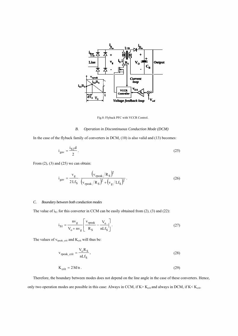
Figure 8 shows a flyback PFC with VCCR Control. The analysis carried out here for this converter is also valid
for SEPIC, Cuk and zeta PFCs. In these cases, (3) is also valid and (4) and (7) become:
d1
iinLfV 1S
o2S
S−
−= , (22)
d2
iii 1S2Sgav
+= , (23)
and from (2), (3), (22) and (23), we can obtain:
( ) ⎥⎦
⎤⎢⎣
⎡−
+=
S
o
S
rpeak2
go
oggav nLf2
V
R
v
nvV
Vnvi . (24)
Clock
Ramp
E/A + in
CC
R1
Low-pass filter
+ VDC
RB
CLF
Integrator
+
-
vramp
+
-
CD
RD
0.5vrpeak
Q1
Q2
+
-vEA
Reset
RLF
Clock
Ramp
E/A + in
CC
R1
Low-pass filter
+ VDC
RB
CLF
Integrator
+
-
+
-
vramp
+
-
CD
RD
0.5vrpeak
Q1
Q2
+
-vEA
+
-vEA
Reset
RLF
(a) (b)
Fig.7: Implementation of the VCCR Control for a boost PFC using two different solutions to determine the vrpeak value: a) Peak detector. b)
Low-pass filter.
vrpeak
TS
iS1RS
tdTS
iS2RS
ig
-VCCR Controller
Vref
+Line
CB
vg
+
-
iline
Output
Av
Voltage feedback loop
Current loop
VO
+
-
iS
iD
vEA
1:n
RS
vrpeak
TS
iS1RS
tdTS
iS2RS
vrpeak
TS
iS1RS
tdTS
iS2RS
ig
-VCCR Controller
Vref
+Line
CB
vg
+
-
iline
Output
Av
Voltage feedback loop
Current loop
VO
+
-
iS
iD
vEA
1:n
RS
ig
-VCCR Controller
Vref
+Line
CB
vg
+
-
iline
Output
Av
Voltage feedback loop
Current loop
VO
+
-
iS
iD
vEA
1:nig
-VCCR Controller
Vref
+Line
CB
vg
+
-
iline
Output
Av
Voltage feedback loop
Current loop
VO
+
-
iS
iD
vEA
ig
-VCCR Controller
Vref
+Line
CB
vg
+
-
iline
Output
AvAv
Voltage feedback loop
Current loop
VO
+
-
iS
iD
vEA
1:n
RS
Fig.8: Flyback PFC with VCCR Control.
B. Operation in Discontinuous Conduction Mode (DCM)
In the case of the flyback family of converters in DCM, (10) is also valid and (13) becomes:
2
dii 2Sgav = . (25)
From (2), (3) and (25) we can obtain:
( )( ) ( )2Sg
2Srpeak
2Srpeak
S
ggav
LfvRv
Rv
Lf2
vi
+⋅= . (26)
C. Boundary between both conduction modes
The value of iS1 for this converter in CCM can be easily obtained from (2), (3) and (22):
⎥⎦
⎤⎢⎣
⎡−
+=
S
o
S
rpeak
go
g1S nLf
V
R
v
nvV
nvi . (27)
The values of vrpeak_crit and Kcrit will thus be:
S
Sorpeak_crit nLf
RVv = , (28)
M/n2Kcrit = . (29)
Therefore, the boundary between modes does not depend on the line angle in the case of these converters. Hence,
only two operation modes are possible in this case: Always in CCM, if K> Kcrit and always in DCM, if K< Kcrit.

It should be noted that the shape of the line current waveform in CCM (24) does not depend on the value of vrpeak;
it only depends on the values of VO, VgP and n. In other words, this shape does not depend on K, but only depends on
M/n, as is shown in Fig. 9a. For values of M/n selected for a standard design (between 0.5 and 1.5), the values of the
THD and PF are not very desirable, as Fig. 9b shows.
However, examination of these waveforms shows that the main difference between them and a perfect sinusoidal
waveform occurs just near the zero crossing, the waveform obtained being higher than the sinusoidal. This means that
the duty cycle value obtained with VCCR Control and a linear ramp is excessive and a less distorted waveform could be
obtained if the duty cycle were lower. A lower duty cycle near the zero crossing can be easily obtained if the linear
ramp is substituted by an exponential ramp.
V. INPUT CURRENT STATIC ANALYLIS WITH AN EXPONENTIAL RAMP
The line current waveforms obtained in the case of the flyback family of converters (Fig.9a) can be improved if
an exponential ramp is used instead of a linear one (Fig. 10). In this case, (2) is not valid and the relationship
between vrpeak, iS2 and d is:
μ
μdμ
S
rpeak2S e1
eeR
vi −
−
−
−−⋅= , (30)
where τ=μ ST , τ being the time constant of the exponential ramp.
M/n=0.5
M/n=0.75M/n=1M/n=1.25M/n=2.5
ωLt0 π0
1
1.2M/n=0.5
M/n=0.75M/n=1M/n=1.25M/n=2.5
ωLt0 π
M/n=0.5
M/n=0.75M/n=1M/n=1.25M/n=2.5
ωLt0 π0
1
1.2
0
1
1.2
0.4 0.8 1.2 1.60
10
20
30
40
50
0.9
0.92
0.94
0.96
0.98
1
PF
2M/n
THD [%]
0.4 0.8 1.2 1.60
10
20
30
40
50
0
10
20
30
40
50
0.9
0.92
0.94
0.96
0.98
1
0.9
0.92
0.94
0.96
0.98
1
PF
2M/n
THD [%]
(a) (b)
Fig.9: a) Line waveforms in a flyback PFC with VCCR Control operating in CCM. b) PF and THD values as a function of M/n.

A. Operation in Continuous Conduction Mode (CCM)
From (3), (22), (23) and (30), we can obtain the values of igav and iS1 in CCM:
⎥⎥⎥⎥
⎦
⎤
⎢⎢⎢⎢
⎣
⎡
+−
−
−
+= −
−+−
)nv(VLf2
vV
)e(1R
)e(ev
nvV
Vgavi
goS
goμ
S
μμ
)nv(VV
rpeak
go
ogo
o
, (31)
)nv(VLf
vV
)e(1R
)e(evi
goS
goμ
S
μμ
)nv(VV
rpeak1S
go
o
+−
−
−= −
−+−
. (32)
B. Operation in Discontinuous Conduction Mode (DCM)
In DCM operation we can calculate the values of iS1, iS2 and igav, from (10), (25) and (30). However, we obtain a
transcendent equation that must be numerically solved.
C. Operation in Discontinuous Conduction Mode (DCM)
The limits between CCM and DCM can be found from (32):
μee
e1
)nv(VLf
vRVv
μ)nv(V
V
μ
goS
gSorpeak_crit
o
o
−+−
−
−
−⋅
+=
g
. (33)
This equation can be rewritten as follows:
vrpeak-vramp
tiSRS
vrpeak
t
vrpeak
iSRS
vrpeak-vramp
tiSRS
vrpeak
vrpeak-vramp
vrpeak-vramp
tiSRS
vrpeak
t
vrpeak
iSRS
vrpeak-vramp
tiSRS
vrpeak
vrpeak-vramp
Fig.10: Main control waveforms for different line angle, from the zero crossing (top) to the peak line (bottom) for VCCR Control with an
exponential compensation ramp.

μμ
)tsinωn(MM
μ
L
Lcrit
ee
e1
)tsinωn(M
tsinωM2K
L −−−
−⋅
+=
+
−
. (34)
As (34) shows, Kcrit has different values depending on the line angle. Hence, the maximum value of Kcrit is:
μcrit_maxen
)eM(12K
μ
−
−−=
μ. (35)
and the minimum value of Kcrit is:
μμ
n)(MM
μ
crit_min
ee
e1
n)(M
M2K
−+−
−
−
−⋅
+= . (36)
Therefore, the PFC operates in CCM for the entire line angle if K >Kcrit_max. Figure 11a shows the waveforms in
CCM for several values of μ and the same design conditions (M/n=0.7, K=2Kcrit_max), whereas the THD for different
values of M/n and μ are given in Fig. 11.b (in this case, K=2Kcrit_max as well). The value of μ which optimizes the
THD for any design case was obtained using a Mathcad spreadsheet. The results are shown in Fig. 11c.
The value of μ must be chosen in order to minimize THD at nominal conditions, which are the conditions to
comply with the regulations. However, if the PFC operates in a different point to the nominal one then the converter
can operate in three modes: always in CCM, always in DCM and in both modes. Figure 12a shows line current
waveforms for the above mentioned design (M/n=0.7, K=2Kcrit_max and μ=5.304) when the value of K changes.
μ=1μ=10
K=2Kcrit_max
M/n=0.7
SinusLinear ramp
ωLt0 π0
11.1
μ=1μ=10
K=2Kcrit_max
M/n=0.7
SinusLinear ramp
ωLt0 π
μ=1μ=10
K=2Kcrit_max
M/n=0.7
SinusLinear ramp
ωLt0 π0
11.1
4 5 6 7
0
5
10
15
μ
M/n=0.5
M/n=0.75
M/n=1M/n=1.25
M/n=1.75
M/n=1.25
THD [%]
K=2Kcrit_max
4 5 6 70
5
10
15
μ
M/n=0.5
M/n=0.75
M/n=1M/n=1.25
M/n=1.75
M/n=1.25
THD [%]
K=2Kcrit_max
3
4
5
6
0.5 1 1.5 2M/n
K=Kcrit_max
K=4Kcrit_max
K=2Kcrit_max
K=1.5Kcrit_max
μ
3
4
5
6
3
4
5
6
0.5 1 1.5 2M/n
K=Kcrit_max
K=4Kcrit_max
K=2Kcrit_max
K=1.5Kcrit_max
μ
(a) (b) (c)
Fig.11: a) Normalized line current for different values of μ. b) THD as a function of μ when K=2Kcrit_max.c) Values of μ to minimize the THD
for different design conditions (M/n and K).
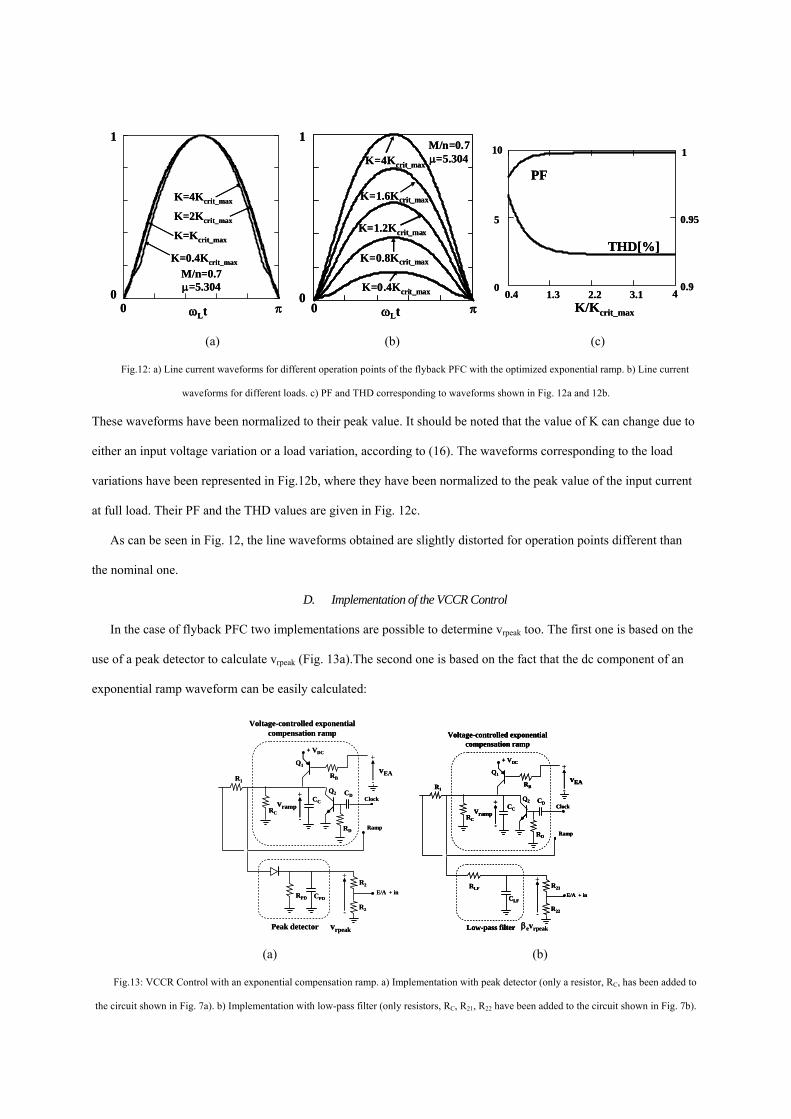
These waveforms have been normalized to their peak value. It should be noted that the value of K can change due to
either an input voltage variation or a load variation, according to (16). The waveforms corresponding to the load
variations have been represented in Fig.12b, where they have been normalized to the peak value of the input current
at full load. Their PF and the THD values are given in Fig. 12c.
As can be seen in Fig. 12, the line waveforms obtained are slightly distorted for operation points different than
the nominal one.
D. Implementation of the VCCR Control
In the case of flyback PFC two implementations are possible to determine vrpeak too. The first one is based on the
use of a peak detector to calculate vrpeak (Fig. 13a).The second one is based on the fact that the dc component of an
exponential ramp waveform can be easily calculated:
ωLt0 π
M/n=0.7μ=5.304
K=4Kcrit_max
K=2Kcrit_max
K=Kcrit_max
K=0.4Kcrit_max
0
1
ωLt0 π
M/n=0.7μ=5.304
K=4Kcrit_max
K=2Kcrit_max
K=Kcrit_max
K=0.4Kcrit_max
0
1
ωLt0 π
K=4Kcrit_max
K=1.6Kcrit_max
K=1.2Kcrit_max
K=0.8Kcrit_max
K=0.4Kcrit_max
M/n=0.7μ=5.304
0
1
ωLt0 π
K=4Kcrit_max
K=1.6Kcrit_max
K=1.2Kcrit_max
K=0.8Kcrit_max
K=0.4Kcrit_max
M/n=0.7μ=5.304
0
1
0.4 1.3 2.2 3.1
0
5 0.95
110
0.9
K/Kcrit_max
PF
THD[%]
40.4 1.3 2.2 3.10
5 0.95
110
0.9
K/Kcrit_max
PF
THD[%]
4
(a) (b) (c)
Fig.12: a) Line current waveforms for different operation points of the flyback PFC with the optimized exponential ramp. b) Line current
waveforms for different loads. c) PF and THD corresponding to waveforms shown in Fig. 12a and 12b.
CC
R1
Peak detector
RPD
+ VDC
RB
CPD
R2
R2
+
-
vramp
+
-
CD
RD
vrpeak
Q1
Q2
RC
Voltage-controlled exponential compensation ramp
Clock
Ramp
E/A + in
+
-vEA
CC
R1
Peak detector
RPD
+ VDC
RB
CPD
R2
R2
+
-
+
-
vramp
+
-
CD
RD
vrpeak
Q1
Q2
RC
Voltage-controlled exponential compensation ramp
Clock
Ramp
E/A + in
+
-vEA
CC
R1
Low-pass filter
RLF
+ VDC
RB
CLF
R21
R22
+
-
vramp
+
-
CD
RD
Q1
Q2
RC
Voltage-controlled exponential compensation ramp
Clock
Ramp
E/A + in
+
-vEA
βevrpeak
CC
R1
Low-pass filter
RLF
+ VDC
RB
CLF
R21
R22
+
-
vramp
+
-
CD
RD
Q1
Q2
RC
Voltage-controlled exponential compensation ramp
Clock
Ramp
E/A + in
+
-vEA
CC
R1
Low-pass filter
RLF
+ VDC
RB
CLF
R21
R22
+
-
+
-
vramp
+
-
CD
RD
Q1
Q2
RC
Voltage-controlled exponential compensation ramp
Clock
Ramp
E/A + in
+
-vEA
+
-vEA
βevrpeak
(a) (b)
Fig.13: VCCR Control with an exponential compensation ramp. a) Implementation with peak detector (only a resistor, RC, has been added to
the circuit shown in Fig. 7a). b) Implementation with low-pass filter (only resistors, RC, R21, R22 have been added to the circuit shown in Fig. 7b).

rpeakerpeak
μ
ramp vvμe11v β=⎟⎟
⎠
⎞⎜⎜⎝
⎛ −−=
−
. (37)
As (37) shows, vrpeak can be easily obtained from the average value of the exponential ramp.
VI. EXPERIMENTAL RESULTS
Two prototypes of PFCs controlled by the proposed method were built and tested. Their control was implemented
using an IC UC3824, which is a controller for peak current-mode dc-dc converters. Some low cost external elements
(Fig.7 and Fig. 13) were added to complete the overall controller. Moreover, some additional bias voltages (not
shown in Fig. 7) were used to allow the use of the aforementioned IC.
Boost case: The main characteristics of this converter are: vg RMS = 110V, VO = 200V, PO = 250W and fS=80 kHz.
Figure 14 shows the main results obtained at full load and different line frequencies (from 60Hz to 1kHz) for the two
different ways to determine the ramp peak value. Figure 15 shows the waveforms at 60 Hz for different load
conditions. As it was expected, the line waveforms are very similar to the ones obtained in [21] with OCC, using an
IC IR1150. The waveforms given in Fig. 14 and in Fig. 15 show that the power factor is very high in all operating
conditions. Table 1 shows the harmonic content of the input current and the compliance with IEC 1000-3-2
regulations at nominal input voltage and full load.
Finally, Fig. 16 shows the main control waveforms with a low-pass filter to determinate the peak value of the
Peak detector Low-pass filter
Harmonic order
RMS current
(A)
Limits Class (A)
Limits Class C
(A)
Limits Class D
(A)
Harmonic order
RMS current
(A)
Limits Class (A)
Limits Class C
(A)
Limits Class D
(A)3 0,336 2,300 0,052 0,850 3 0,333 2,300 0,051 0,850 5 0,092 1,140 0,770 0,475 5 0,083 1,140 0,766 0,475 7 0,035 0,770 0,258 0,250 7 0,028 0,770 0,257 0,250 9 0,021 0,400 0,180 0,125 9 0,005 0,400 0,180 0,125
11 0,019 0,330 0,129 0,088 11 0,007 0,330 0,129 0,088 13 0,017 0,210 0,077 0,074 13 0,012 0,210 0,077 0,074 15 0,011 0,150 0,016 0,064 15 0,011 0,150 0,016 0,064 17 0,010 0,132 0,016 0,057 17 0,010 0,132 0,016 0,057 19 0,010 0,118 0,016 0,051 19 0,008 0,118 0,016 0,051 21 0,008 0,107 0,016 0,046 21 0,007 0,107 0,016 0,046 23 0,007 0,098 0,016 0,042 23 0,007 0,098 0,016 0,042 25 0,007 0,090 0,016 0,039 25 0,006 0,090 0,016 0,039 27 0,006 0,083 0,016 0,036 27 0,006 0,083 0,016 0,036 29 0,005 0,078 0,016 0,033 29 0,005 0,078 0,016 0,033 31 0,005 0,073 0,016 0,031 31 0,005 0,073 0,016 0,031 33 0,005 0,068 0,016 0,029 33 0,050 0,068 0,016 0,029 35 0,004 0,064 0,016 0,028 35 0,004 0,064 0,016 0,028 37 0,004 0,061 0,016 0,026 37 0,004 0,061 0,016 0,026 39 0,003 0,058 0,016 0,025 39 0,004 0,058 0,016 0,025
Table 1: Harmonic content in the prototypes of boost PFC.

controlled linear ramp. As this figure shows, the input current and control waveforms match with the static study
presented in this paper.
60Hz PF=0.996 THD=8.84%
1 A/div 5 ms/div
240Hz PF=0.996 THD=9.18%
1 A/div 1 ms/div
400Hz PF=0.995 THD=10.1%
1A/div 500 μs/div
1000Hz PF=0.994 THD=10.5%
1 A/div 200 μs/div
60Hz PF=0.996 THD=8.84%
1 A/div 5 ms/div1 A/div 5 ms/div
240Hz PF=0.996 THD=9.18%
1 A/div 1 ms/div1 A/div 1 ms/div
400Hz PF=0.995 THD=10.1%
1A/div 500 μs/div
1000Hz PF=0.994 THD=10.5%
1 A/div 200 μs/div
(a) (b)
Fig. 14: Boost case: Line current at full load (250 W) for different line frequencies. a) Peak detector. b) Low-pass filter
250W PF=0.996 THD=8.84%
1 A/div 5 ms/div
125W PF=0.993 THD=11.5%
1 A/div 5 ms/div
55W PF=0.991 THD=13.8%
1 A/div 5 ms/div
40W PF=0.981 THD=19.8%
1 A/div 5 ms/div
250W PF=0.996 THD=8.84%
1 A/div 5 ms/div1 A/div 5 ms/div
125W PF=0.993 THD=11.5%
1 A/div 5 ms/div1 A/div 5 ms/div
55W PF=0.991 THD=13.8%
1 A/div 5 ms/div
40W PF=0.981 THD=19.8%
1 A/div 5 ms/div
(a) (b)
Fig. 15: Boost case: Line current at full load (250 W) for different line frequencies. a) Peak detector. b) Low-pass filter
Fig. 16: a) Control waveforms using the low-pass filter

Flyback case: The main characteristics of this converter are: vg RMS = 110V, VO = 12V, PO = 50W and fS=80 kHz.
This prototype was only implemented with the low-pass filter technique. Figure 17a shows the line current at full
load for different line frequencies, whereas Fig. 17b shows the waveforms for different load conditions. The
harmonic content of the input current and the harmonic limits according with IEC 1000-3-2 are given in Table 2.
Harmonic order
RMS current (A)
Limits Class (A)
Limits Class C (A)
Limits Class D (A)
3 0,027 2,300 0,010 0,170 5 0,012 1,140 0,156 0,095 7 0,001 0,770 0,052 0,050 9 0,003 0,400 0,037 0,025 11 0,005 0,330 0,026 0,018 13 0,005 0,210 0,016 0,015 15 0,004 0,150 0,016 0,013 17 0,004 0,132 0,016 0,011 19 0,004 0,118 0,016 0,010 21 0,003 0,107 0,016 0,009 23 0,002 0,098 0,016 0,008 25 0,002 0,090 0,016 0,008 27 0,002 0,083 0,016 0,007 29 0,002 0,078 0,016 0,007 31 0,001 0,073 0,016 0,006 33 0,001 0,068 0,016 0,006 35 0,001 0,064 0,016 0,006 37 0,000 0,061 0,016 0,005 39 0,000 0,058 0,016 0,005
Table 2: Harmonic content in the prototype of flyback PFC.
VII. CONCLUSION
A new method to implement One-Cycle Control in CCM PFCs has been presented in this paper. The method is
based on the use of standard controllers for peak current-mode converters, employing neither an analog multiplier
nor an input voltage sensor. Therefore this control method is useful for designing relatively low-cost PFCs .This
60Hz PF=0.994 THD=10.7%
0.2 A/div 5 ms/div
240Hz PF=0.992 THD=12.3%
0.2 A/div 1 ms/div
400Hz PF=0.992 THD=13.1%
0.2 A/div 1 ms/div
1000Hz PF=0.992 THD=13.5%
0.2 A/div 500 μs/div
60Hz PF=0.994 THD=10.7%
0.2 A/div 5 ms/div0.2 A/div 5 ms/div
240Hz PF=0.992 THD=12.3%
0.2 A/div 1 ms/div0.2 A/div 1 ms/div
400Hz PF=0.992 THD=13.1%
0.2 A/div 1 ms/div
1000Hz PF=0.992 THD=13.5%
0.2 A/div 500 μs/div
(a) (b)
Fig. 17: a) Flyback case: Line current at full load (250 W) for different line frequencies. b) Flyback case: Line current at 60 Hz for different
output powers

implementation can be used not only with the boost PFC, but it can be easily adapted for its use with the flyback
family of converters, by employing an exponential ramp, instead of a linear one.
The results obtained show that PFs in the range of 0.99 have been measured at full load, whereas they slightly
decrease at light load (0.98). In all cases the THD is better than 22% and the compliance with the IEC 61000-3-2
regulations is guarantied (in all Classes).
Moreover, the input current feedback loop is extremely fast, thus allowing this type of control to be used with
relatively high frequency lines. The experimental results also show excellent PFs (0.99) and THD (better than 13%)
at high lines frequencies and full load.
ACKNOWLEDGMENT
This research has been supported by the Spanish Ministry of Education and Science under project TEC2007-
66917/MIC and grant AP2006-04777.

REFERENCES
[1] M. J. Kocher and R. L. Steigerwald, “An ac-to-dc converter with high quality input waveforms”, IEEE Trans. Ind.
Appl., vol. 19, no. 4 1983, pp. 586-599.
[2] L. H. Dixon, “High power factor preregulators for off-line power supplies”, Unitrode Power Supply Design
seminar, 1990, pp I2-1 to I2-16.
[3] K. H. Liu and Y. L. Lin, “Current waveform distortion in power factor correction circuits employing
discontinuous-mode boost converter”, IEEE PESC 1989, pp. 825-829.
[4] R. Erickson, M. Madigan and S. Singer, “Design of a simple high-power-factor rectifier based on the flyback
converter”, IEEE APEC 1990, pp. 792-801.
[5] J. Sebastián, J. Uceda, J. A. Cobos, J. Arau, and F. Aldana, “Improving power factor correction in distributed
power supply systems using PWM and ZCS-QR SEPIC topologies”, IEEE PESC 1991, pp. 780–791.
[6] M. Brkovic and S. Cuk, “Input current shaper using Cuk converter”, IEEE INTELEC, 1992, pp. 532–539.
[7] D. S. L. Simonetti, J. Sebastián and J. Uceda, “The discontinuous conduction mode SEPIC and Cuk power factor
preregulators: Analysis and design”, IEEE Trans. Ind. Electron., vol. 44, no. 4, 1998, pp. 727-738.
[8] J. Sebastián, J. A. Martínez, J. M. Alonso, and J. A. Cobos, “Voltage-Follower control in zero-current-switched
quasi-resonant power factor preregulators”, IEEE Trans. Power Electron. vol. 13, no. 5, 1997, pp. 630-637.
[9] J. Lazar and S. Cuk, “Open loop control of a unity power factor, discontinuous conduction mode rectifier”, IEEE
INTELEC 1995, pp. 671-677.
[10] D. Maksimovic, Y. Jang and R. Erickson, “Nonlinear-carrier control for high power factor boost rectifier”,
IEEE Trans. Power Electron., 1996, vol.11, no. 4, pp. 578-584.
[11] R. Zane and D. Maksimovic, “Nonlinear-carrier control for high-power-factor rectifiers based on up–down
switching converters”, IEEE Trans. Power Electron., 1998, vol.13, no. 2, pp. 213-221.
[12] S. Buso, G. Spiazzi and D. Tagliavia, “Simplified control technique for high-power-factor flyback, Cuk and
SEPIC rectifiers operating in CCM”, IEEE Trans. Ind. Appl., 2000, vol. 36, no. 5, pp. 1413-1418.
[13] J. Sebastián, A. Fernández, P. Villegas, J. A. Martínez and E. de la Cruz, “A new low-cost control technique for
power factor correctors operating in continuous conduction mode”, IEEE PESC, 2002, pp. 1132-1136.

[14] J. Sebastián, A. Fernández, M. M. Hernando and D. G. Lamar, “Simple control and high efficiency in the boost
converter used to shape the line current to comply with the IEC 61000-3-2 Regulations”, IEEE APEC, 2005, pp.
1163-1169.
[15] J. Sebastián, J. A. Cobos, J. M. Lopera and J. Uceda, “The determination of the boundaries between continuous
and discontinuous conduction mode in PWM dc-to-dc converters used as power factor preregulators”, IEEE Trans.
Power Electron., 1995, vol.10, no. 5, pp. 574-582.
[16] D. Maksimovic, Y. Jang and R. Erickson, “Nonlinear-carrier control for high power factor boost rectifier”,
IEEE Trans. Power Electron., 1996, vol.11, no. 4, pp. 578-584.
[17] R. Zane and D. Maksimovic, “Nonlinear-carrier control for high-power-factor rectifiers based on up–down
switching converters”, IEEE Trans. Power Electron., 1998, vol.13, no. 2, pp. 213-221.
[18] K. M. Smedley and S. Cuk, “One-Cycle control of switching converters”, IEEE Trans. Power Electron., 1995,
vol.10, no. 6, pp. 625-633.
[19] J. P. Gegner and C. Q. Lee, “Linear peak current mode control: a simple active power factor correction control
technique”, IEEE PESC 1996, pp. 196-202.
[20] Z. Lai and K. M. Smedley, “A general constant-frequency pulsewidth modulator and its applications”, IEEE
Trans. Circuits and Systems-I: Fundamental Theory and Applications, vol. 45, no. 4, April 1998, pp. 386-396.
[21] Z. Lai and K. M. Smedley, “A family of continuous-conduction-mode power-factor-correction controllers based
on the general pulse-width modulator”, IEEE Trans. Power Electron., vol. 13, no. 3, May 1998, pp. 501-510.
[22] R. Brown and M. Soldano “One Cycle Control IC Simplifies PFC Designs”, IEEE APEC, 2005, pp. 825-829.
[23] Electromagnetic compatibility (EMC)-part 3: Limits-section 2: Limits for harmonic current emissions
(equipment input current<16A per phase), IEC1000-3-2 Document, 1995.
[24] Draft of the proposed CLC Common Modification to IEC 61000-3-2 Ed. 2.0:20