Embed Size (px)
Citation preview

Materia1 and processing issues for the monolithic integration of microelectronics with surface-micromachined polysilicon sensors and actuators
J. H. Smith, S . Montague, and J. J. Sniegowski 4
Integrated Micromechanics, Microsensors, and CMOS Technology Department Sandia National Laboratories
Albuquerque, NM 87185-1080
ABSTRACT
The monolithic integration of micromechanical devices with their controlling electronics offers potential increases in performance as well as decreases in cost for these devices. Analog Devices has demonstrated the commercial viability of this integration by interleaving the micromechanical fabrication steps of an accelerometer with the microelectronic fabrication steps of its controlling electronics. Sandia's Microelectronics Development Laboratory has integrated the micromechanical and microelectronic processing sequences in a segregated fashion. In this CMOS-first, micromechanics-last approach, conventional aluminum metallization is replaced by tungsten metallization to allow the CMOS to withstand subsequent high-temperature
at U.C. Berkeley. processing during the micromechanical fabrication. This approach is a further development of an approach originally developed
Specifically, the issues of yield, repeatability, and uniformity of the tungstedCMOS approach are addressed. Also, material issues related to the development of high-temperature diffusion barriers, adhesion layers, and low-stress films are discussed. Processing and material issues associated with alternative approaches to this integration such as micromechanics-first, CMOS-last or the interleaved process are also discussed.
Keywords: micromechanics, CMOS, integration, tungsten, smart sensors
1. INTRODUCTION
Recently, a great deal of interest has developed in manufacturing processes that allow the monolithic integration of microelectromechanical structures (MEMS) with driving, control, and signal processing electronics. This integration promises to improve ihe performance of micromechanical devices as well as the cost of manufacturing, packaging, and instrumenting these devices by combining the micromechanical devices with an electronic subsystem in the same manufacturing and packaging process. For example, Analog Devices has developed and marketed an accelerometer' which illustrates the viability and commercial potential of this integration. They accomplished this task by interleaving, combining, and customizing their manufacturing processes which produce the micromechanical devices with the processes that produce the electronics. Researchers at Berkelef have developed a modular integrated approach in which the aluminum metallization of CMOS is - replaced with tungsten to enable the CMOS to withstand subsequent micromechanical processing.
2. INTEGRATION STRATEGIES
As presented in a recent review of integrated polysilicon microsystems3, there are three basic approaches to monolithically integrating surface micromachined polysilicon devices with their controlling electronics: microelectronics-first,.' interleaved, and micromechanics-first. Each of these strategies must overcome the limitations of the processing requirements of - - both the microelectronic and micromechanical devices. Polysilicon micromechanical devices often have large vertical topologiec (typically 4 to 10 microns in height) and require long, high-temperature anneals for stress relaxation (such as 3 hours at 1100°C). Microelectronic devices use precision photolithographic techniques that require planar substrates. They also have thermal processing budgets limited by dopant diffusion and metallization.
DISTRIBUTION OF THiS DOCUMENT IS UNUMED - -
Smith I

DISCLAIMER
Portions of this document may be illegible in electronic image products. Images are produced from the best available original document.

The microelectronics-first approach overcomes planarity restraint imposed by the photolithographic processes by building the microelectronics before the non-planar micromechanical devices. The limitation on thermal budget of the microelectronic devices remains as a problem. Although the dopant diffusion problem mitigated by changing the fabrication technology, the aluminum metallization used in conventional microelectronic technologies melts at the temperatures needed for polysilicon anneals. To overcome the temperature limitation of the aluminum metallization, researchers at Berkeley have prototyped an all-tungsten CMOS process. After having completed this process, the micromechanical devices are fabricated. A cross-sectional diagram of a modified version of the Berkeley process is shown in Figure 1. Unfortunately, the temperature of the polysilicon anneal is limited by the lack of a robust diffusion barrier to prevent formation of tungsten silicide during this anneal and by high stress of the tungsten film stack.
CMOS Device Area 4 b
AI Bond
Micromechanical Device Area 4 b
Mechanical Poly
TIN Anchor Pol Pad
N+ antimonydoped substrate
Figure 1. A cros-sectional view of the CMOS-first approach to micromechanical integration where tungsten metallization replaces the conventional aluminum metallization.
The interleaved approach may be the most economical approach for large-scale manufacturing since it optimizes and combines the manufacturing processes of both the micromechanical devices and the microelectronic devices. This optimized manufacturing mix imposes limits on both the microelectronic device performance and the micromechanical device performance. It also requires extensive changes to the overall manufacturing flow in order to accomadate changes in just the microelectronic devices or the micromechanical devices. This limits the usefulness of this approach for rapid prototyping of different technologies or development work. -
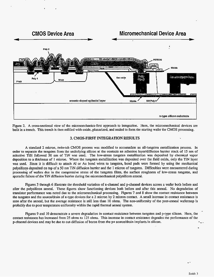
Finally, a third approach to integration may be pursued. This micromechanics-first approach fabricates, anneals, and planarizes the micromechanical devices before the microelectronic devices are fabricated. Since the micromechanical devices are both annealed and planarized before the microelectronic device fabrication steps are reached, the topology and thermal processing limitations of the microelectronic devices are overcome. Figure 2 illustrates a micromechanics-first approach to integration that - will be reported elsewhere! In this technology, micromechanical devices are fabricated in trenches etched in silicon wafers. These trenches are then refilled with oxide, planarized with chemical-mechanical polishing, annealed, and sealed. These wafers then form the starting material for a conventional microelectronic fabrication process. This approach may also have advantages=- - in packaging of finished devices.
CMOS Device Area Micromechanical Device Area
Poly 2 4
arsenic-doped epitaxial layer
n-type silicon substrate
Figure 2. A cross-sectional view of the micromechanics-first approach to integration. Here, the micromechanical devices are built in a trench. This trench is then refilled with oxide, planarized, and sealed to form the starting wafer for CMOS processing.
3. CMOS-FIRST INTEGRATION RESULTS
A standard 2 micron, twin-tub CMOS process was modified to accomadate an all-tungsten metallization process. In order to separate the tungsten from the underlying silicon at the contacts an adhesion layer/diffusion barrier stack of 15 nm of selective TiSi followed 50 nm of TiN was used. The low-stress tungsten metallization was deposited by chemical vapor deposition to a thickness of 1 micron. Where the tungsten metallization was deposited over the field oxide, only the TiN layer was used, Since it is difficult to attach AI or Au bond wires to tungsten, bond pads were formed by using the mechanical polysilicon deposited on top of a 50 nm TIN diffusion barrier and the 1 micron of tungsten. Difficulties were encountered during processin'g of wafers due to the compressive stress of the tungsten films, the surface roughness of low-stress tungsten, and sporadic failure of the TIN diffusion barrier during the micromechanical polysilicon anneal.
Figures 3 through 6 illustrate the threshold variation of n-channel and p-channel devices across a wafer both before and after the polysilicon anneal. These figures show functioning devices both before and after this anneal. No degradation of transistor performance was noted due to the micromechanical processing. Figures 7 and 8 show the contact resistance between the tungsten and the sourcddrain of n-type devices for a 2 micron by 2 micron contact. A small increase in contact resistance is seen after the anneal, but the average resistance is still less than 10 ohms. The non-uniformity of the post-anneal wafermap is probably due to poor temperature uniformity within the rapid thermal anneal system.
Figures 9 and 10 demonstrate a severe degradation in contact resistance between tungsten and p-type silicon. Here, the contact resistance has increased from 25 ohms to 125 ohms. This increase in contact resistance degrades the performance of the p-channel devices and may be due to out-diffusion of boron from the p+ source/drain implants in silicon. - -
.-
Sniirh 3

2.0 E
Figure 3. Threshold voltage wafer map for n-channel devices before the micromechanical anneal.
Figure 4. Threshold voltage wafer map for n-channel devices after the micromechanical anneal.
.- Slllllll 4

i
Figure 5. Threshold voltage wafer map for p-channel devices before the micromechanical anneal.
- -
Figure 6. Threshold voltage wafer map for p-channel devices after the micromechanical anneal.
- -
Smith 5

250
200
7 150 A=
3 # f 100- rz
1
Figure 8. Wafermap of contact resistance between tungsten and n-type silicon after the micromechanical anneal
-
-
-

Figure 9.
IY/ 200
0
Wafermap of contact resistance between tungsten and p-type silicon before the micromechanical anneal
1ooc
Figure IO. Wafermap of contact resistance between tungsten and p-type silicon after the micromechanical anneal. Note change of scale.

The compressive stress of the bondpad stack was seen to cause delamination, or lifting, of the bondpads. Thin interconnect lines did not exhibit this lifting, but the 100 micron by 100 micron bondpads showed significant delamination. Figure 11 illustrates this phenomena. The delamination is seen to occur between the field oxide and the silicon substrate. Figure 12 shows a cross-section of the delaminated bondpad in more detail. Starting from the bottom, the materials seen in this stack are TEOS-based field oxide, TIN, tungsten, porous W i S i (formed by the failure of the upper Tm diffusion*barrier), WSi, and micromechanical polysilicon.
In lowering the stress of the tungsten metallization by varying the deposition conditions, the .surface roughness of the film was increased significantly. This prevented the projection steppers used for photolithography from being used to pattern the tungsten. A manually-aligned contact aligner was used instead.
Despite these processing difficulties, the devices were fabricated were funcbonal as long as their size was relatively small. A larger device, an accelerometer with on-chip preamplifiers is shown’ in Figure 13. The CMOS on this chip was fully- functional, but the temperature limitations imposed by the lack of a robust diffusion barrier caused the polysilicon to curl. For large polysilicon devices this curl prevented the micromechanical devices from being fully-functional. Devices under 200 microns in size did not see significant curling.
Because of the problems encountered in attempting to bring this technology to a manufacturing facility, we have decided to try other approaches besides the all-tungsten, CMOS-first integration approach.
- - Figure I I . Focused ion beam cross-section of tungsten bondpad showing delamination of bondpad stack at the center of the contact due to compressive stress of bondpad stack.
_ -
Smith S

Figure 12. Close-up view
- - Figure 13. A surface-micromachined polysilicon accelerometer with integrated control electronics fabricated using the all- tungsten, CMOS-first approach to integration.
- -
Smith 0

4.. SUMMARY
This report was prepared as an account of work sponsored by an agency of the United States Government. Neither the United States Government nor any agency thereof, nor any of their employees, makes any warranty, express or implied, or assumes any legal liability or responsi- bility for the accuracy, completeness, or usefulness of any information, apparatus, product, or process disclosed, or represents that its use would not infringe privately owned rights. Refer- ence herein to any specific commercial product, process, or service by trade name. trademark, manufacturer. or otherwise does not necessarily constitute or imply its endorsement, recom- mendation, or favoring by the United States Government or any agency thereof. The views and opinions of authors expressed herein do not necessarily state or reflect those of the United States Government or any agency thereof.
- -
Micromechanical structures require long, high-temperature anneals to assure that the stress in the structural materials of the micromechanical structures has completely relaxed. On the other hand, CMOS technology requires planarity of the substrate to achieve high-resolution in the photolithographic process. If the micromechanical processing is performed,first, the substrate planarity is sacrificed. If the CMOS is built first, it (and its metallization) must withstand the high-temperature anneals of the micromechanical processing. This second alternative was chosen by researchers at Berkeley and has been further developed as presented here. In this approach, the standard aluminum metal used in CMOS was replaced with tungsten. Since tungsten is a refractory metal, it withstands the high-temperature processing, but a number of issues remain unsolved doncerning with adhesion of the tungsten layer and the unwanted formation of tungsten silicides. Despite these issues, devices integrated with functioning control electronics have been fabricated.
a
A unique micromechanics-first approach is also being developed. - In this approach, micromechanical devices are fabricated in a trench etched on the surface of the wafer. After these devices are complete, the trench is refilled with oxide, planarized using chemical-mechanical polishing, and sealed with a nitride membrane. The wafer with the embedded micromechanical devices is then processed using conventional CMOS processing. Additional steps are added at the end of the CMOS process in order to expose and release the embedded micromechanical devices.
5. ACKNOWLEDGMENTS
This work, performed at Sandia National Laboratories, was supported by the U.S. Department of Energy under contract DE-AC04-94AL85000. The process development engineers, operators, and technicians of the Microelectronics Development Laboratory should also be acknowledged for their contributions to the process development, fabrication, and testing of these devices.
6. REFERENCES
‘W. Kuehnel and S . Sherman, “A surface micromachined silicon accelerometer with on-chip detection circuitry,” Sensors and ActitatorsA, vol. 45, no. 1, pp. 7-16 (1994). ’W. Yun, R. Howe, and P. Gray, “Surface micromachined, digitally force-balanced accelerometer with integrated CMOS detection circuitry,” Proc. IEEE Solid-Srate Sensor and Actuator Workshop ‘92, p. 126 (1992). 3R. Howe, “Polysilicon integrated microsystems: Technologies and applications,” Proc. Transducers ‘95, pp. 43-46 (1 995). 4J. Smith, S . Montague, J. Sniegowski, and P. McWhorter, “Embedded micromechanical devices for the monolithic integration of MEMS with CMOS,” submitted to the 1995 Infernafiunaf Electron Device Meeting.
DISCLAIMER