Embed Size (px)
Citation preview
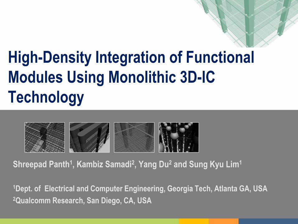
High-Density Integration of Functional
Modules Using Monolithic 3D-IC
Technology
Shreepad Panth1, Kambiz Samadi2, Yang Du2 and Sung Kyu Lim1
1Dept. of Electrical and Computer Engineering, Georgia Tech, Atlanta GA, USA 2Qualcomm Research, San Diego, CA, USA
2/32
• Introduction to monolithic 3D
• Prior work and contributions
• Design and analysis methodology
• Post-layout comparisons with 2D and TSV-based 3D
– Footprint, Wirelength, Timing and Power
• Conclusions
Outline
3/32
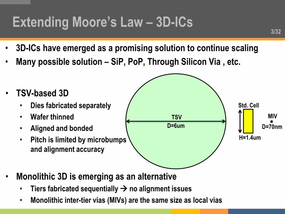
• 3D-ICs have emerged as a promising solution to continue scaling
• Many possible solution – SiP, PoP, Through Silicon Via , etc.
Extending Moore’s Law – 3D-ICs
• TSV-based 3D
• Dies fabricated separately
• Wafer thinned
• Aligned and bonded
• Pitch is limited by microbumps
and alignment accuracy
• Monolithic 3D is emerging as an alternative
• Tiers fabricated sequentially no alignment issues
• Monolithic inter-tier vias (MIVs) are the same size as local vias
TSV
D=6um
H=1.4um
Std. Cell
MIV
D=70nm

4/32 Monolithic 3D – Fabrication Methods
• Epitaxial growth[2]
• Wafer bonding[3]
[2] S.-M. Jung, H. Lim, K. Kwak, and K. Kim, “ 500-MHz DDR High-Performance 72-Mb 3-D SRAM …” in IEEE Trans. on Electron Devices, 2010.
[3] P. Batude et al., “Advances in 3D CMOS Sequential Integration,” in Proc. IEEE Int. Electron Devices Meeting, 2009.
5/32
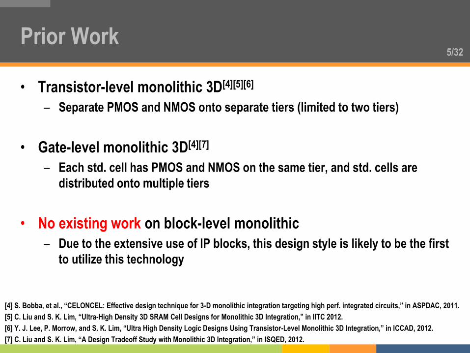
• Transistor-level monolithic 3D[4][5][6]
– Separate PMOS and NMOS onto separate tiers (limited to two tiers)
• Gate-level monolithic 3D[4][7]
– Each std. cell has PMOS and NMOS on the same tier, and std. cells are
distributed onto multiple tiers
• No existing work on block-level monolithic
– Due to the extensive use of IP blocks, this design style is likely to be the first
to utilize this technology
Prior Work
[4] S. Bobba, et al., “CELONCEL: Effective design technique for 3-D monolithic integration targeting high perf. integrated circuits,” in ASPDAC, 2011.
[5] C. Liu and S. K. Lim, “Ultra-High Density 3D SRAM Cell Designs for Monolithic 3D Integration,” in IITC 2012.
[6] Y. J. Lee, P. Morrow, and S. K. Lim, “Ultra High Density Logic Designs Using Transistor-Level Monolithic 3D Integration,” in ICCAD, 2012.
[7] C. Liu and S. K. Lim, “A Design Tradeoff Study with Monolithic 3D Integration,” in ISQED, 2012.
6/32
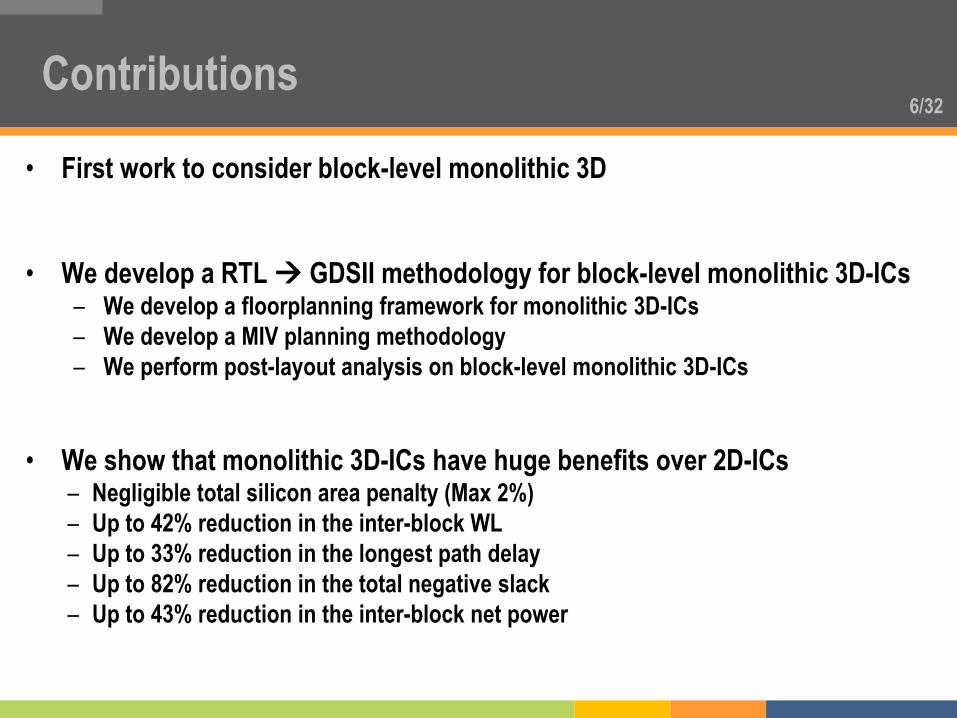
• First work to consider block-level monolithic 3D
• We develop a RTL GDSII methodology for block-level monolithic 3D-ICs – We develop a floorplanning framework for monolithic 3D-ICs
– We develop a MIV planning methodology
– We perform post-layout analysis on block-level monolithic 3D-ICs
• We show that monolithic 3D-ICs have huge benefits over 2D-ICs – Negligible total silicon area penalty (Max 2%)
– Up to 42% reduction in the inter-block WL
– Up to 33% reduction in the longest path delay
– Up to 82% reduction in the total negative slack
– Up to 43% reduction in the inter-block net power
Contributions
7/32
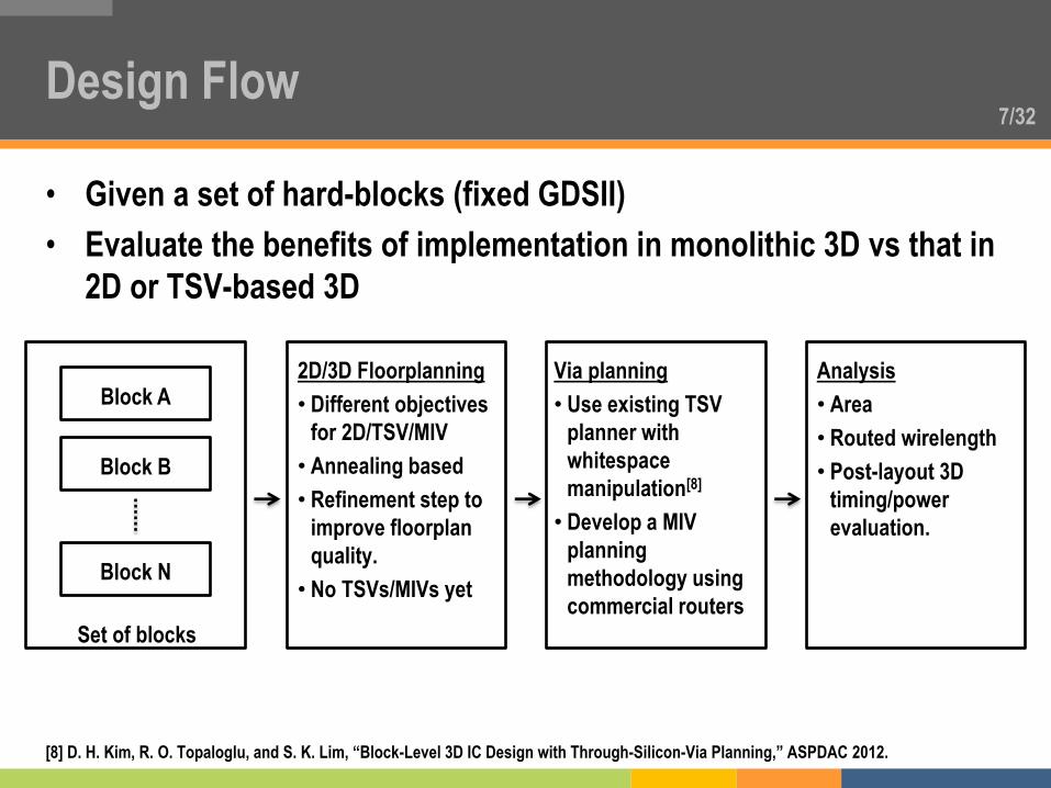
• Given a set of hard-blocks (fixed GDSII)
• Evaluate the benefits of implementation in monolithic 3D vs that in
2D or TSV-based 3D
Design Flow
Block A
Block B
Block N
Set of blocks
2D/3D Floorplanning
• Different objectives
for 2D/TSV/MIV
• Annealing based
• Refinement step to
improve floorplan
quality.
• No TSVs/MIVs yet
Via planning
• Use existing TSV
planner with
whitespace
manipulation[8]
• Develop a MIV
planning
methodology using
commercial routers
Analysis
• Area
• Routed wirelength
• Post-layout 3D
timing/power
evaluation.
[8] D. H. Kim, R. O. Topaloglu, and S. K. Lim, “Block-Level 3D IC Design with Through-Silicon-Via Planning,” ASPDAC 2012.
8/32
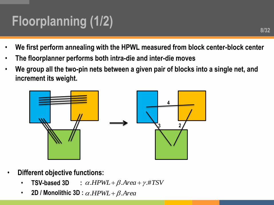
• We first perform annealing with the HPWL measured from block center-block center
• The floorplanner performs both intra-die and inter-die moves
• We group all the two-pin nets between a given pair of blocks into a single net, and
increment its weight.
Floorplanning (1/2)
4
2 3
• Different objective functions:
• TSV-based 3D :
• 2D / Monolithic 3D :
TSVAreaHPWL .#..
AreaHPWL ..
9/32
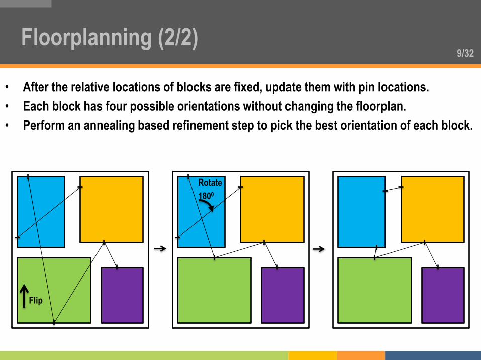
• After the relative locations of blocks are fixed, update them with pin locations.
• Each block has four possible orientations without changing the floorplan.
• Perform an annealing based refinement step to pick the best orientation of each block.
Floorplanning (2/2)
Flip
Rotate
1800
10/32
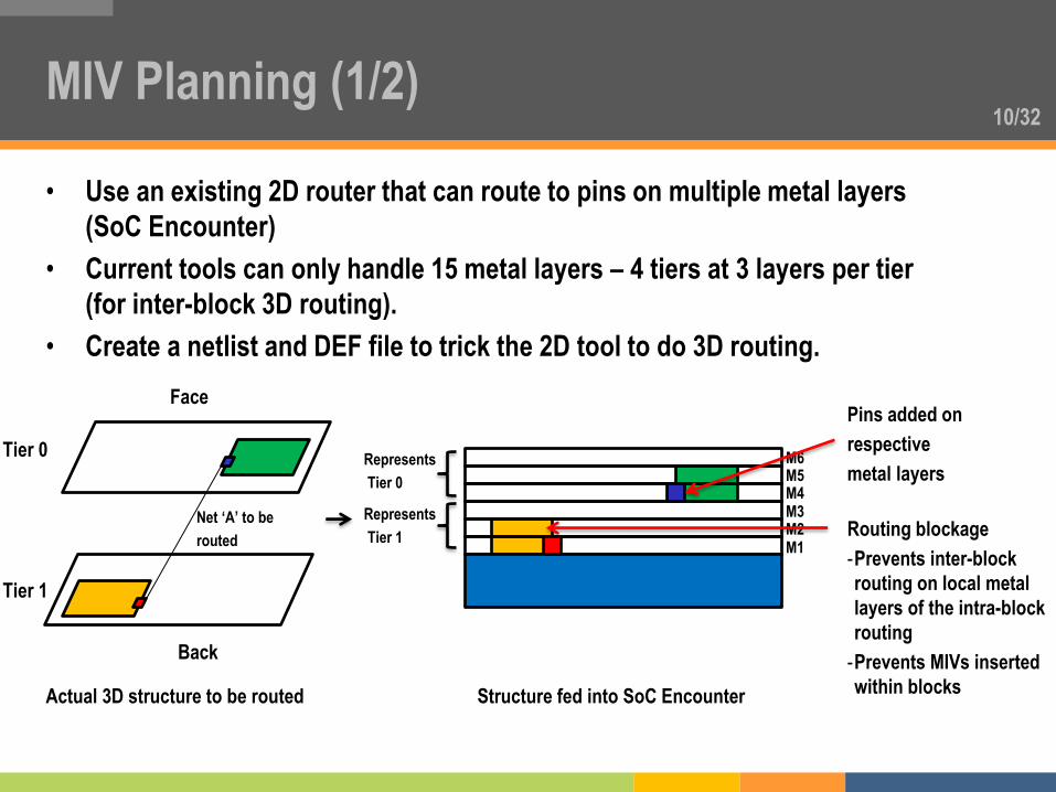
• Use an existing 2D router that can route to pins on multiple metal layers
(SoC Encounter)
• Current tools can only handle 15 metal layers – 4 tiers at 3 layers per tier
(for inter-block 3D routing).
• Create a netlist and DEF file to trick the 2D tool to do 3D routing.
MIV Planning (1/2)
Net ‘A’ to be
routed
Tier 0
Tier 1
Face
Back
Actual 3D structure to be routed
M6
M5
M4
M3
M2
M1
Represents
Tier 0
Represents
Tier 1
Pins added on
respective
metal layers
Routing blockage
-Prevents inter-block
routing on local metal
layers of the intra-block
routing
-Prevents MIVs inserted
within blocks Structure fed into SoC Encounter
11/32
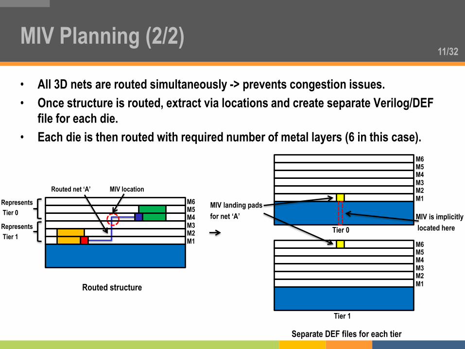
• All 3D nets are routed simultaneously -> prevents congestion issues.
• Once structure is routed, extract via locations and create separate Verilog/DEF
file for each die.
• Each die is then routed with required number of metal layers (6 in this case).
MIV Planning (2/2)
Routed net ‘A’
M6
M5
M4
M3
M2
M1
Represents
Tier 0
Represents
Tier 1
MIV location
M6
M5
M4
M3
M2
M1
M6
M5
M4
M3
M2
M1
Routed structure
Separate DEF files for each tier
Tier 0
Tier 1
MIV landing pads
for net ‘A’ MIV is implicitly
located here
12/32
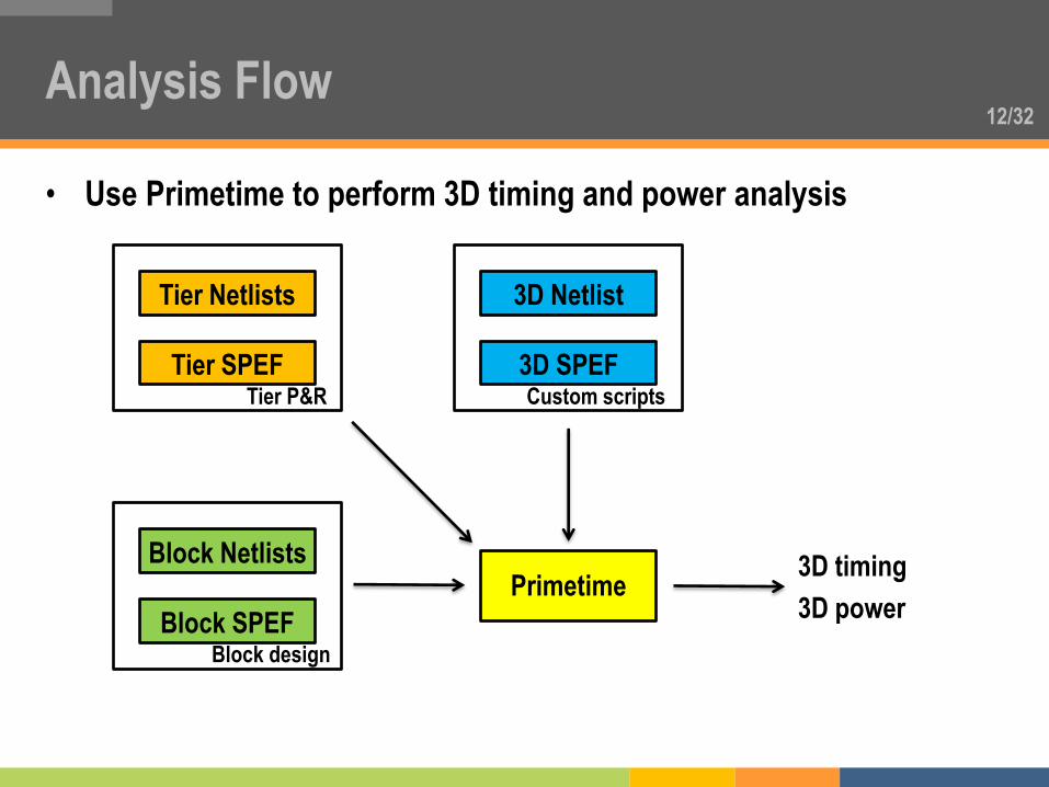
• Use Primetime to perform 3D timing and power analysis
Analysis Flow
Tier Netlists
Tier SPEF Tier P&R
Block Netlists
Block SPEF Block design
3D Netlist
3D SPEF Custom scripts
Primetime
3D timing
3D power
13/32
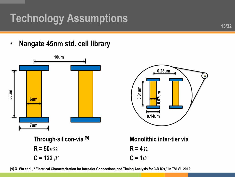
• Nangate 45nm std. cell library
Technology Assumptions
10um
6um
7um
50u
m
0.28um
0.07
um
0.14um
0.31
um
Through-silicon-via [9]
R = 50
C = 122 fF
m
Monolithic inter-tier via
R = 4
C = 1 fF
[9] X. Wu et al., “Electrical Characterization for Inter-tier Connections and Timing Analysis for 3-D ICs,” in TVLSI 2012
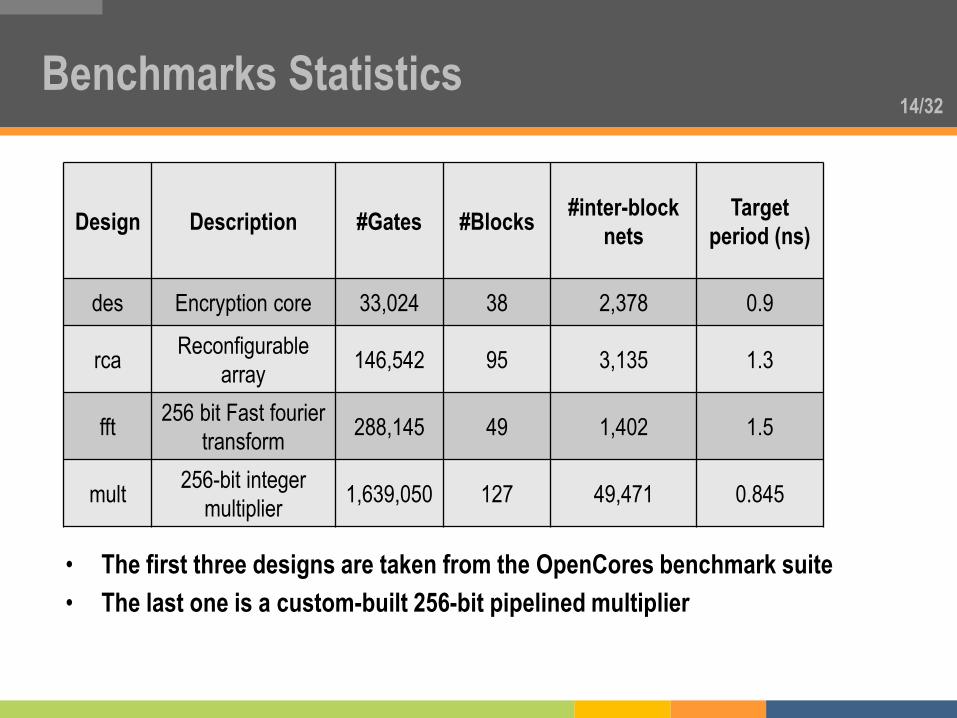
14/32 Benchmarks Statistics
Design Description #Gates #Blocks #inter-block
nets
Target
period (ns)
des Encryption core 33,024 38 2,378 0.9
rca Reconfigurable
array 146,542 95 3,135 1.3
fft 256 bit Fast fourier
transform 288,145 49 1,402 1.5
mult 256-bit integer
multiplier 1,639,050 127 49,471 0.845
• The first three designs are taken from the OpenCores benchmark suite
• The last one is a custom-built 256-bit pipelined multiplier
15/32
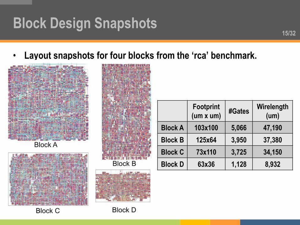
• Layout snapshots for four blocks from the ‘rca’ benchmark.
Block Design Snapshots
Footprint
(um x um) #Gates
Wirelength
(um)
Block A 103x100 5,066 47,190
Block B 125x64 3,950 37,380
Block C 73x110 3,725 34,150
Block D 63x36 1,128 8,932
16/32
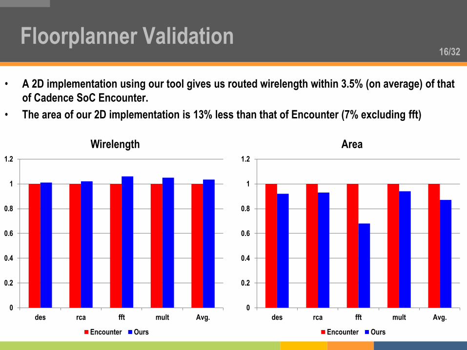
• A 2D implementation using our tool gives us routed wirelength within 3.5% (on average) of that
of Cadence SoC Encounter.
• The area of our 2D implementation is 13% less than that of Encounter (7% excluding fft)
Floorplanner Validation
0
0.2
0.4
0.6
0.8
1
1.2
des rca fft mult Avg.
Area
Encounter Ours
0
0.2
0.4
0.6
0.8
1
1.2
des rca fft mult Avg.
Wirelength
Encounter Ours
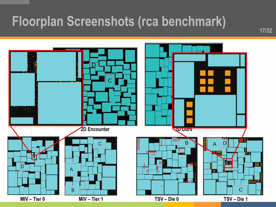
17/32 Floorplan Screenshots (rca benchmark)
2D Encounter 2D Ours
MIV – Tier 0 MIV – Tier 1 TSV – Die 0 TSV – Die 1
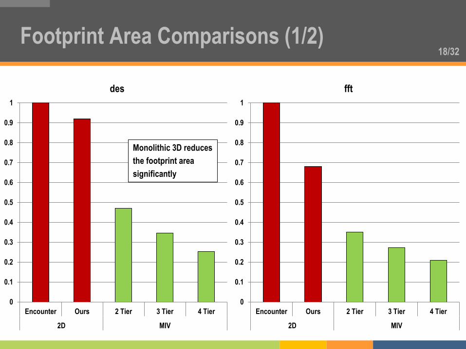
18/32 Footprint Area Comparisons (1/2)
0
0.1
0.2
0.3
0.4
0.5
0.6
0.7
0.8
0.9
1
Encounter Ours 2 Tier 3 Tier 4 Tier
2D MIV
des
0
0.1
0.2
0.3
0.4
0.5
0.6
0.7
0.8
0.9
1
Encounter Ours 2 Tier 3 Tier 4 Tier
2D MIV
fft
Monolithic 3D reduces
the footprint area
significantly
19/32 Footprint Area Comparisons (2/2)
0.2
0.4
0.6
0.8
1
1.2
1.4
1.6
1.8
2
2.2
En
cou
nte
r
Ou
rs
2 T
ier
3 T
ier
4 T
ier
2 D
ie
3 D
ie
4 D
ie
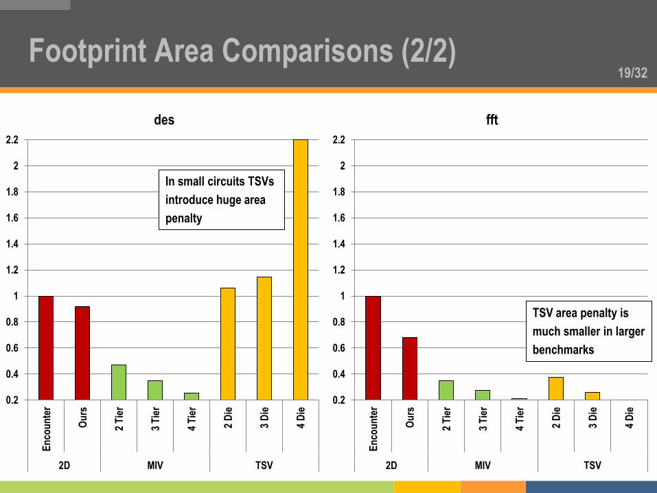
2D MIV TSV
des
0.2
0.4
0.6
0.8
1
1.2
1.4
1.6
1.8
2
2.2
En
cou
nte
r
Ou
rs
2 T
ier
3 T
ier
4 T
ier
2 D
ie
3 D
ie
4 D
ie
2D MIV TSV
fft
In small circuits TSVs
introduce huge area
penalty
TSV area penalty is
much smaller in larger
benchmarks
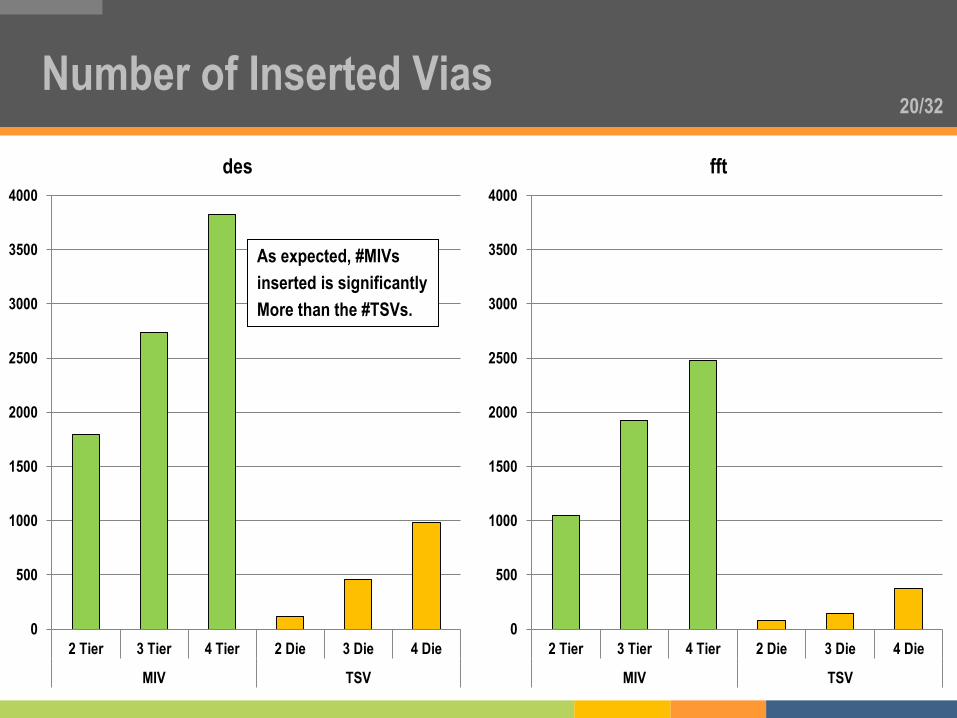
20/32 Number of Inserted Vias
0
500
1000
1500
2000
2500
3000
3500
4000
2 Tier 3 Tier 4 Tier 2 Die 3 Die 4 Die
MIV TSV
des
0
500
1000
1500
2000
2500
3000
3500
4000
2 Tier 3 Tier 4 Tier 2 Die 3 Die 4 Die
MIV TSV
fft
As expected, #MIVs
inserted is significantly
More than the #TSVs.
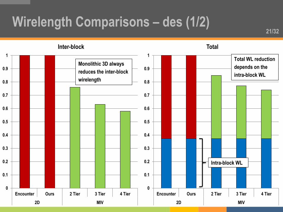
21/32 Wirelength Comparisons – des (1/2)
0
0.1
0.2
0.3
0.4
0.5
0.6
0.7
0.8
0.9
1
Encounter Ours 2 Tier 3 Tier 4 Tier
2D MIV
Inter-block
0
0.1
0.2
0.3
0.4
0.5
0.6
0.7
0.8
0.9
1
Encounter Ours 2 Tier 3 Tier 4 Tier
2D MIV
Total
Monolithic 3D always
reduces the inter-block
wirelength
Total WL reduction
depends on the
intra-block WL
Intra-block WL
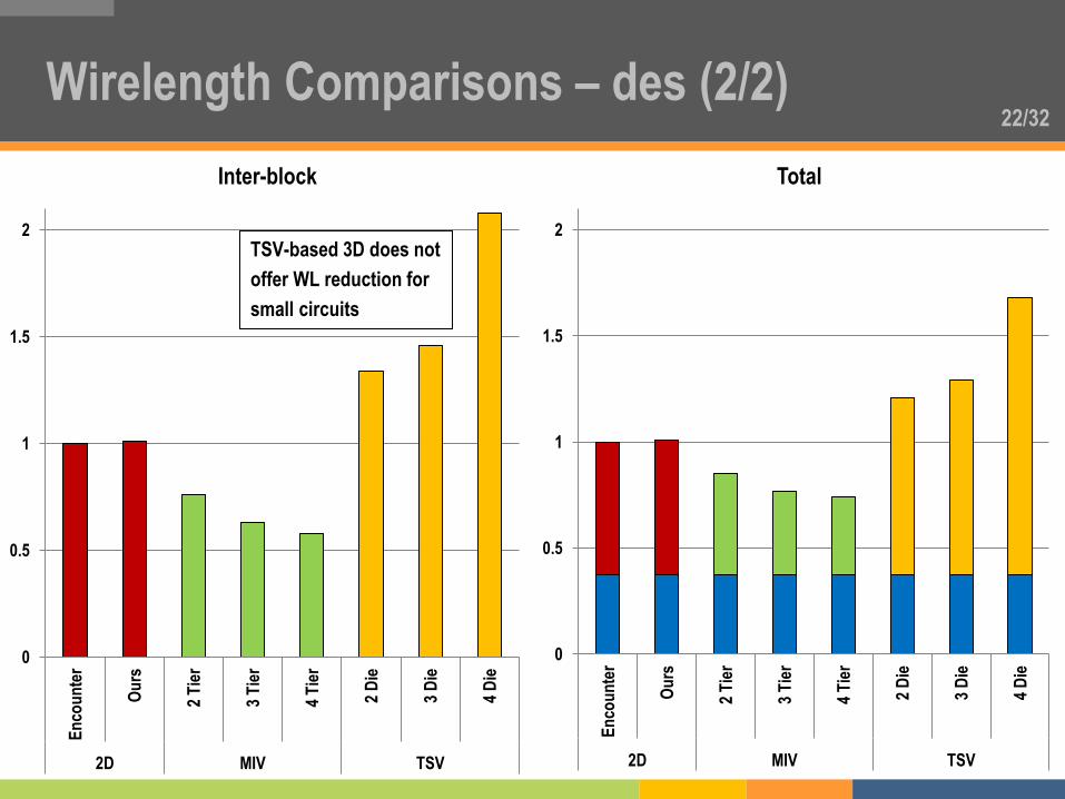
22/32 Wirelength Comparisons – des (2/2)
0
0.5
1
1.5
2
En
cou
nte
r
Ou
rs
2 T
ier
3 T
ier
4 T
ier
2 D
ie
3 D
ie
4 D
ie
2D MIV TSV
Inter-block
0
0.5
1
1.5
2
En
cou
nte
r
Ou
rs
2 T
ier
3 T
ier
4 T
ier
2 D
ie
3 D
ie
4 D
ie
2D MIV TSV
Total
TSV-based 3D does not
offer WL reduction for
small circuits
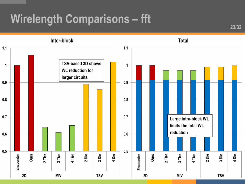
23/32 Wirelength Comparisons – fft
0.5
0.6
0.7
0.8
0.9
1
1.1
En
cou
nte
r
Ou
rs
2 T
ier
3 T
ier
4 T
ier
2 D
ie
3 D
ie
4 D
ie
2D MIV TSV
Inter-block
0.5
0.6
0.7
0.8
0.9
1
1.1
En
cou
nte
r
Ou
rs
2 T
ier
3 T
ier
4 T
ier
2 D
ie
3 D
ie
4 D
ie
2D MIV TSV
Total
TSV-based 3D shows
WL reduction for
larger circuits
Large intra-block WL
limits the total WL
reduction
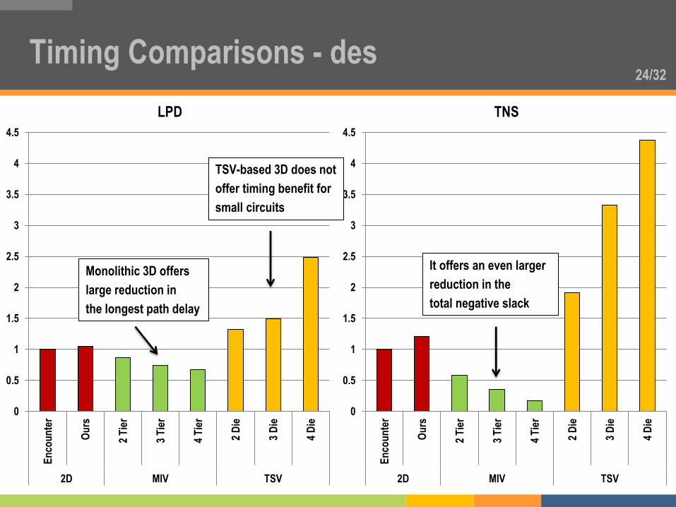
24/32 Timing Comparisons - des
0
0.5
1
1.5
2
2.5
3
3.5
4
4.5
En
cou
nte
r
Ou
rs
2 T
ier
3 T
ier
4 T
ier
2 D
ie
3 D
ie
4 D
ie
2D MIV TSV
LPD
0
0.5
1
1.5
2
2.5
3
3.5
4
4.5
En
cou
nte
r
Ou
rs
2 T
ier
3 T
ier
4 T
ier
2 D
ie
3 D
ie
4 D
ie
2D MIV TSV
TNS
Monolithic 3D offers
large reduction in
the longest path delay
It offers an even larger
reduction in the
total negative slack
TSV-based 3D does not
offer timing benefit for
small circuits
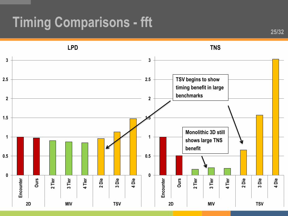
25/32 Timing Comparisons - fft
0
0.5
1
1.5
2
2.5
3
En
cou
nte
r
Ou
rs
2 T
ier
3 T
ier
4 T
ier
2 D
ie
3 D
ie
4 D
ie
2D MIV TSV
LPD
0
0.5
1
1.5
2
2.5
3
En
cou
nte
r
Ou
rs
2 T
ier
3 T
ier
4 T
ier
2 D
ie
3 D
ie
4 D
ie
2D MIV TSV
TNS
Monolithic 3D still
shows large TNS
benefit
TSV begins to show
timing benefit in large
benchmarks
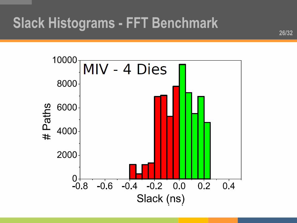
26/32 Slack Histograms - FFT Benchmark
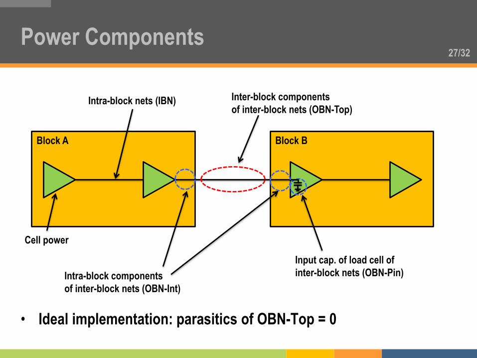
27/32 Power Components
Block B Block A
Intra-block nets (IBN)
Intra-block components
of inter-block nets (OBN-Int)
Inter-block components
of inter-block nets (OBN-Top)
Input cap. of load cell of
inter-block nets (OBN-Pin)
• Ideal implementation: parasitics of OBN-Top = 0
Cell power
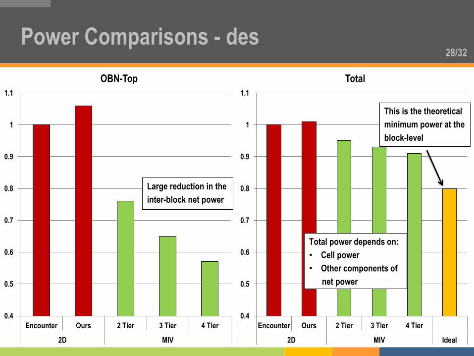
28/32 Power Comparisons - des
0.4
0.5
0.6
0.7
0.8
0.9
1
1.1
Encounter Ours 2 Tier 3 Tier 4 Tier
2D MIV
OBN-Top
0.4
0.5
0.6
0.7
0.8
0.9
1
1.1
Encounter Ours 2 Tier 3 Tier 4 Tier
2D MIV Ideal
Total
Large reduction in the
inter-block net power
Total power depends on:
• Cell power
• Other components of
net power
This is the theoretical
minimum power at the
block-level
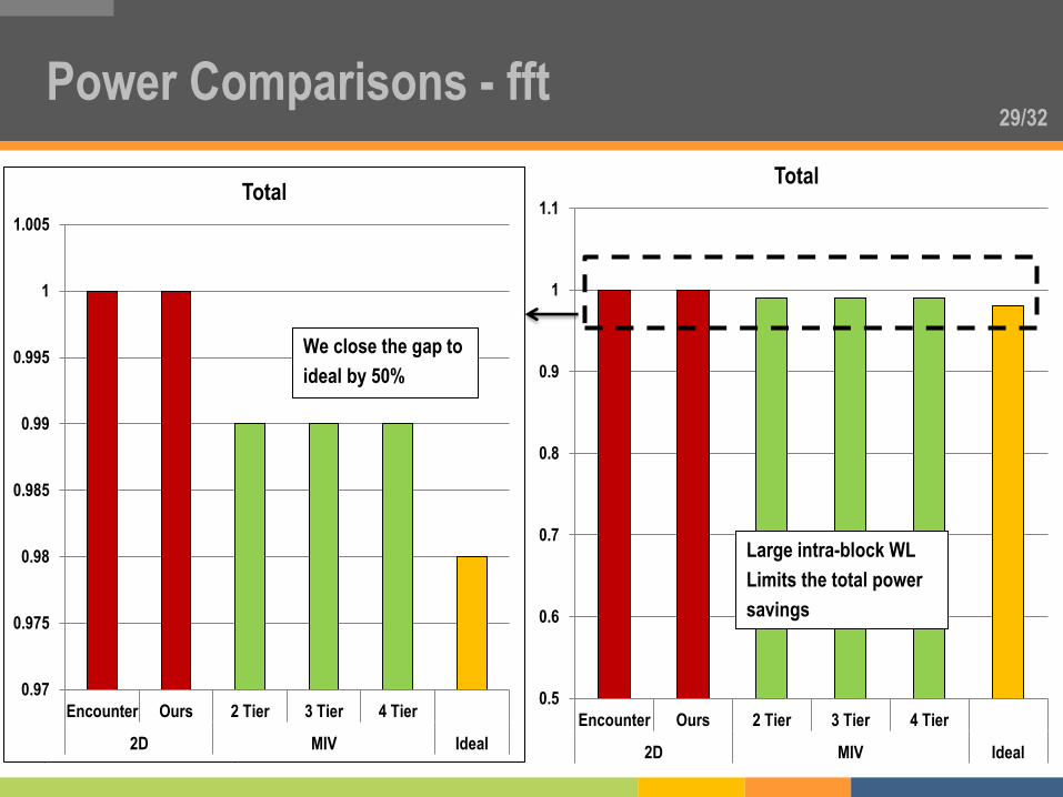
29/32 Power Comparisons - fft
0.5
0.6
0.7
0.8
0.9
1
1.1
Encounter Ours 2 Tier 3 Tier 4 Tier
2D MIV
OBN-Top
0.5
0.6
0.7
0.8
0.9
1
1.1
Encounter Ours 2 Tier 3 Tier 4 Tier
2D MIV Ideal
Total
Large intra-block WL
Limits the total power
savings
0.97
0.975
0.98
0.985
0.99
0.995
1
1.005
Encounter Ours 2 Tier 3 Tier 4 Tier
2D MIV Ideal
Total
We close the gap to
ideal by 50%
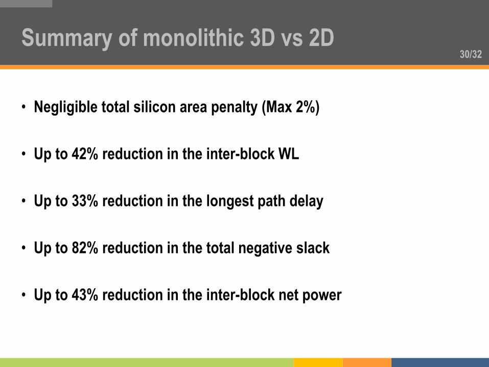
30/32 Summary of monolithic 3D vs 2D
• Negligible total silicon area penalty (Max 2%)
• Up to 42% reduction in the inter-block WL
• Up to 33% reduction in the longest path delay
• Up to 82% reduction in the total negative slack
• Up to 43% reduction in the inter-block net power
31/32
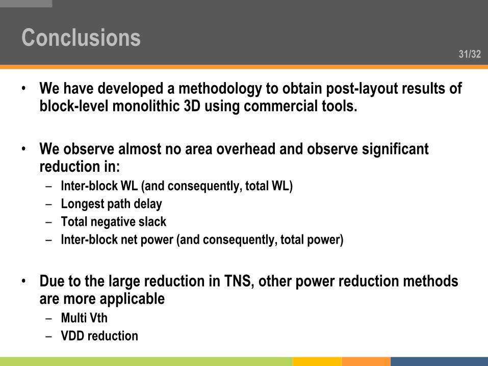
• We have developed a methodology to obtain post-layout results of block-level monolithic 3D using commercial tools.
• We observe almost no area overhead and observe significant reduction in: – Inter-block WL (and consequently, total WL)
– Longest path delay
– Total negative slack
– Inter-block net power (and consequently, total power)
• Due to the large reduction in TNS, other power reduction methods are more applicable – Multi Vth
– VDD reduction
Conclusions

32/32
Thank you.
Questions ?