Embed Size (px)
Citation preview
The Hong Kong Polytechnic University
Department of Applied Physics
Oxide-based Giant Magnetoresistive
Heterostructures
CHENG Wang Fai
A thesis submitted in partial fulfillment of the
requirements for the Degree of Master of Philosophy
August 2007
Abstract
THE HONG KONG POLYTECHNIC UNIVERSITY
__________________________________________________________________________________
i
Abstract
The giant magnetoresistance (GMR) effect was discovered in 1988 in metal
multilayer structures. The effect showed a large magnetoresistance (MR) ratio up to
80% at room temperature in Fe/Cr multilayers. Since then a number of alternative
structures were developed, but they invariably relied on the changes of relative
magnetization directions in the magnetic layers or components to achieve high and low
resistive states. The discovery of GMR effect had a strong impact on the development
of computer memory technology. At present, GMR read heads are used extensively in
hard disk read heads.
In my research project, oxide-based spin valve structures were deposited and
characterized. La0.7Sr0.3MnO3 (LSMO) thin films were fabricated by pulsed laser
deposition. The project consists of two parts. In the first part, the effects of post
annealing on LSMO films, under different oxygen pressures, were examined. During
multilayer fabrication processes, different growth conditions may be necessary for
various layers. Different annealing procedures, sometimes ex situ, have to be performed.
Therefore, the stability of the layers has to be studied, in order to obtain multilayers
Abstract
THE HONG KONG POLYTECHNIC UNIVERSITY
__________________________________________________________________________________
ii
with desirable properties. This part of study provided useful information for
investigations on epitaxial oxide multilayers.
LSMO thin films were deposited by pulsed laser deposition on (100) LaAlO3
(LAO) substrates at 650 °C, with the film thicknesses varying from 20 to 50 nm. The
oxygen pressures used to fabricate the films were 150 (or 100) mTorr. In situ annealing
processes were then performed at 100 (150) mTorr. Curie temperatures (Tc) of the films
were estimated from the peaks of the resistance-temperature (RT) graphs. For LSMO
films deposited at 150 mTorr and annealed at 100 mTorr, Tc of the samples dropped
with an increasing annealing time until about 30 minutes, beyond which the TC started
to increase. For LSMO films deposited at 100 mTorr and annealed at 150 mTorr, no
signs of metal-insulation transition were observed even after 30 minutes of annealing.
Ex situ annealing processes were also performed, testing the stability of LSMO films
under post-deposition heat treatment processes after exposure to ambient conditions.
The Tc of films were found to be strongly dependent on the annealing procedures.
In the second part of the project, pseudo spin valves were fabricated by using
LSMO and Co33Fe67 (CoFe) as ferromagnetic layers. These layers had very different
coercivities, an important criterion for observing GMR effect. In order to reduce
Abstract
THE HONG KONG POLYTECHNIC UNIVERSITY
__________________________________________________________________________________
iii
magnetic coupling between the two ferromagnetic layers, a non-magnetic and
conducting spacer layer is usually required. Recent research has however shown that
pseudo spin valves could be fabricated without using spacer layers. These spacerless
pseudo spin valves, formed by direct deposition of polycrystalline metallic layers on
epitaxial oxides, greatly reduced the difficulty in the fabrication process.
In this part of the project, the magnetotransport property of deposited LSMO\CoFe
structure was investigated. Magnetoresistances of samples were measured in
current-perpendicular-to-plane mode. For single-layer LSMO samples grown on (100)
LAO, a negative magentoresistance behaviour was obtained. After depositing the CoFe,
the magnetoresistance behaviour was changed from negative to positive. One of
possible reasons for the observation is the interfacial layer formed between the metal
and oxide layers, which can be treated as a non-magnetic spacer. The thickness of the
interface layer was sufficiently large to decouple the two ferromagnetic layers. Relative
magnetization directions of the two ferromagnetic layers can be switched independently
by an external magnetic field, according to their corresponding coercivities.
Acknowledgements
THE HONG KONG POLYTECHNIC UNIVERSITY
__________________________________________________________________________________
iv
Acknowledgements
I would like to acknowledge Dr. C. W. Leung, my chief supervisor, for his
guidance and for patiently proofreading this thesis at various stages. I also wish to thank
Dr. J. Y. Dai, my co-supervisor, Dr. K. H. Wong and Dr. C. L. Mak for providing
valuable comments. Special thanks go to Miss. C. Y. Lam, Mr. M. H. Wong and Mr. W.
L. Sin for training me on using the PLD system, XRD, LabView Programming and
VSM. I also thank Mr. Y. K. Chan for his help and discussions on my research work. I
would like to thank my research companions, Mr. H. Y. Kwong, Mr. C. H. Lau and Mr.
W. C. Liu for their useful suggestions.
This work is supported by a grant from the Research Grants Council of the Hong
Kong Special Administrative Region, China (Project No. PolyU 5216/06E), and a
studentship from the Hong Kong Polytechnic University.
Table of Contents
THE HONG KONG POLYTECHNIC UNIVERSITY
__________________________________________________________________________________
v
TABLE OF CONTENTS
Abstract i
Acknowledgments iv
Table of contents v
CHAPTER 1 1
Introduction 1
CHAPTER 2 3
Background review 3
2.1 Magnetoresistance 3
2.1.1 Introduction 3
2.1.2 Ordinary magnetoresistance 4
2.1.3 Anisotropic magnetoresistance 5
2.1.4 Tunneling magnetoresistance 7
2.1.5 Colossal Magnetoresistance 8
Table of Contents
THE HONG KONG POLYTECHNIC UNIVERSITY
__________________________________________________________________________________
vi
2.1.6 Giant magnetoresistance 9
2.1.6.1 Introduction 9
2.1.6.2 Measurement geometry 11
2.1.6.3 Origin of GMR 12
2.1.6.4 Spin valve 16
2.2 Half metallic manganites 20
2.2.1 Introduction 20
2.2.2 Crystal and electronic structures 21
2.2.3 Electron-lattice interaction 23
2.2.4 Exchange interaction 25
2.3 Summary 27
CHAPTER 3 28
Experimental methods 28
3.1 Pulsed laser deposition 28
3.1.1 Introduction 28
3.1.2 Mechanisms of PLD 29
Table of Contents
THE HONG KONG POLYTECHNIC UNIVERSITY
__________________________________________________________________________________
vii
3.1.3 Advantages of PLD 31
3.1.4 Disadvantage of PLD 31
3.1.5 PLD setup 32
3.2 Characterizations and measurements 35
3.2.1 Structural characterization 35
3.2.1.1 X-ray diffractometry (XRD) 35
3.2.1.2 Transmission electron microscopy (TEM) 39
3.2.1.3 Atomic force microscopy (AFM) 40
3.2.2 Magnetic measurements 42
3.2.3 Electrical transport measurements 45
3.2.3.1 Resistance against temperature 45
3.2.3.2 Current against voltage 47
3.2.3.3 Resistance against magnetic field 47
CHAPTER 4 50
Effect of post annealing on La0.7Sr0.3MnO3 thin films 50
4.1 Introduction 50
Table of Contents
THE HONG KONG POLYTECHNIC UNIVERSITY
__________________________________________________________________________________
viii
4.2 Fabrication and Structural Characterization of
LSMO Target 53
4.3 Fabrication of LSMO Thin Films 55
4.4 Structural and Electrical Characterization of
LSMO Thin Films 57
4.5 In situ Post Annealing 61
4.6 Ex situ Post Annealing 67
4.7 Summary 71
CHAPTER 5 73
Manganite\metal spin valves 73
5.1 Introduction 73
5.2 Fabrication of LaNiO3 (LNO) & LNO\LSMO thin films 75
5.3 Structural characterization of LNO
and LNO\LSMO thin films 76
5.4 Surface morphology of LNO and LNO\LSMO thin films 80
5.5 Electrical characterization of LNO thin films 82
Table of Contents
THE HONG KONG POLYTECHNIC UNIVERSITY
__________________________________________________________________________________
ix
5.6 Fabrication of LNO\LSMO\Co33Fe67 trilayer films 83
5.7 Structural characterization of LNO\LSMO\Co33Fe67 films 83
5.8 Magnetic characterization of LNO\LSMO\Co33Fe67 87
5.9 Magneto-transport characterization of LNO\LSMO 90
5.10 Magneto-transport properties of LNO\LSMO\Co33Fe67 94
5.11 Summary 101
CHAPTER 6 102
Conclusions 102
Appendix A 106
Appendix B 107
Appendix C 108
References 109
Chapter 1
THE HONG KONG POLYTECHNIC UNIVERSITY
__________________________________________________________________________________
1
CHAPTER 1
Introduction
Since late 1980s, numerous studies have been made on investigating the origin of
the giant magnetoresistive (GMR) effect and potential enhancement of the
magnetoresistive responses. Commercial devices based on GMR effect, such as read
heads, magnetic field sensors and magnetic memory chips, have become available in the
market. These significant progresses are due to advancements in thin film deposition
techniques, making it possible to fabricate ultrathin layers of various materials with
precise thicknesses.
So far, GMR investigations have been dominated by metallic structures. Metallic
magnetic materials generally have spin polarization values less than 50% [1]. As the
GMR ratio strongly depends on the spin polarization of the materials, perovskite
manganites are good alternative materials due to their fully spin-polarized conduction
bands. In addition, oxides are more tolerant towards extreme working conditions,
making them more attractive for specialized operations.
This thesis is divided into six chapters. Brief reviews on the topics of
magnetoresistance and half-metallic manganites are given in Chapter 2. Experimental
Chapter 1
THE HONG KONG POLYTECHNIC UNIVERSITY
__________________________________________________________________________________
2
techniques used in the project are discussed in details in Chapter 3. These include
heteroepitaxial thin film growth by pulsed laser deposition (PLD), as well as electric
and magnetic characterization techniques. In Chapter 4, I will discuss the fabrication
and characterization of LSMO thin films by PLD; in particular, the post annealing effect
on the properties of LSMO was studied and the results will be presented. In Chapter 5,
details on the fabrication and characterization of LNO\LSMO\Co33Fe67 trilayers will be
presented. Finally, Chapter 6 summarizes the main results and conclusions arising from
this work.
Chapter 2
THE HONG KONG POLYTECHNIC UNIVERSITY
__________________________________________________________________________________
3
CHAPTER 2
Background Review
2.1 Magnetoresistance
2.1.1 Introduction
Magnetoresistance (MR) refers to the change of a material’s resistivity under the
influence of an external magnetic field. It has a variety of physical origins, depending
on the material’s intrinsic and extrinsic properties. MR effect is gaining importance in
technological applications. It is heavily used in magnetic memories, read heads and
magnetic field sensors [2]. In the following, various MR effects will be introduced.
They include ordinary MR, anisotropic MR, tunneling MR, colossal MR, and giant MR.
Generally, the MR ratio is defined as
)0()()0()(
=−=
=H
HHHMRρ
ρρ (2.1.1)
unless otherwise stated.
Chapter 2
THE HONG KONG POLYTECHNIC UNIVERSITY
__________________________________________________________________________________
4
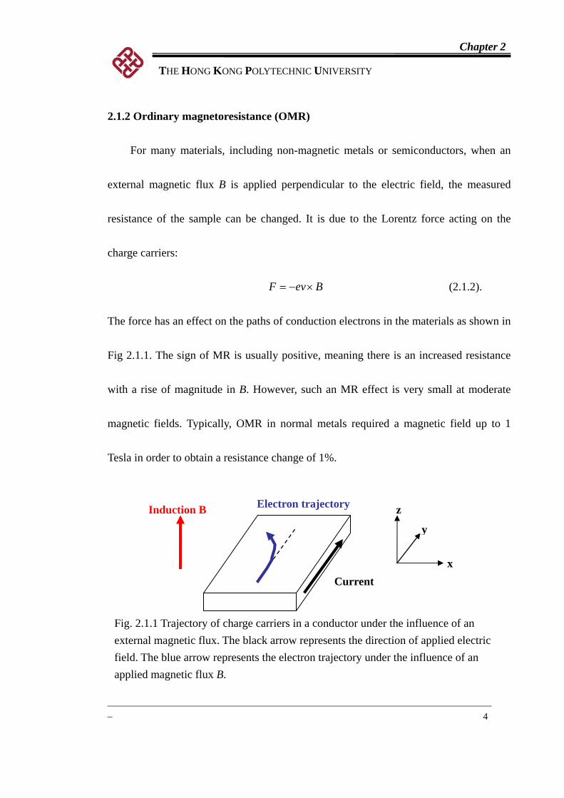
2.1.2 Ordinary magnetoresistance (OMR)
For many materials, including non-magnetic metals or semiconductors, when an
external magnetic flux B is applied perpendicular to the electric field, the measured
resistance of the sample can be changed. It is due to the Lorentz force acting on the
charge carriers:
BevF ×−= (2.1.2).
The force has an effect on the paths of conduction electrons in the materials as shown in
Fig 2.1.1. The sign of MR is usually positive, meaning there is an increased resistance
with a rise of magnitude in B. However, such an MR effect is very small at moderate
magnetic fields. Typically, OMR in normal metals required a magnetic field up to 1
Tesla in order to obtain a resistance change of 1%.
Fig. 2.1.1 Trajectory of charge carriers in a conductor under the influence of an external magnetic flux. The black arrow represents the direction of applied electric field. The blue arrow represents the electron trajectory under the influence of an applied magnetic flux B.
z
y
x Current
Electron trajectory Induction B
Chapter 2
THE HONG KONG POLYTECHNIC UNIVERSITY
__________________________________________________________________________________
5
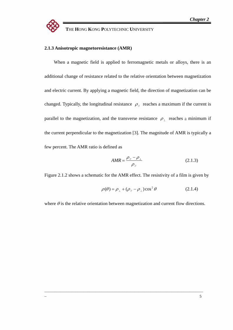
2.1.3 Anisotropic magnetoresistance (AMR)
Wh field is applied to ferromagnetic metals or alloys, there is an
additional change of resistance related to the relative orientation between magnetization
and electric current. By applying a magnetic field, the direction of magnetization can be
c
en a magnetic
hanged. Typically, the longitudinal resistance //ρ reaches a maximum if the cur
arallel to the magnetization, and the transverse resistance ⊥
rent is
p ρ reaches a minimum if
the current perpendicular to the magnetization [3]. The magnitude of AMR is typically a
few percent. The AMR ratio is defined as
//
//
ρρρ ⊥−
=AMR (2.1.3)
Figure 2.1.2 shows a schematic for the AMR effect. The resistivity of a film is given by
θρρρθρ 2// cos)()( ⊥⊥ −+= (2.1.4)
where θ is the relative orientation between magn ization and current flow directions. et
Chapter 2
THE HONG KONG POLYTECHNIC UNIVERSITY
__________________________________________________________________________________
6
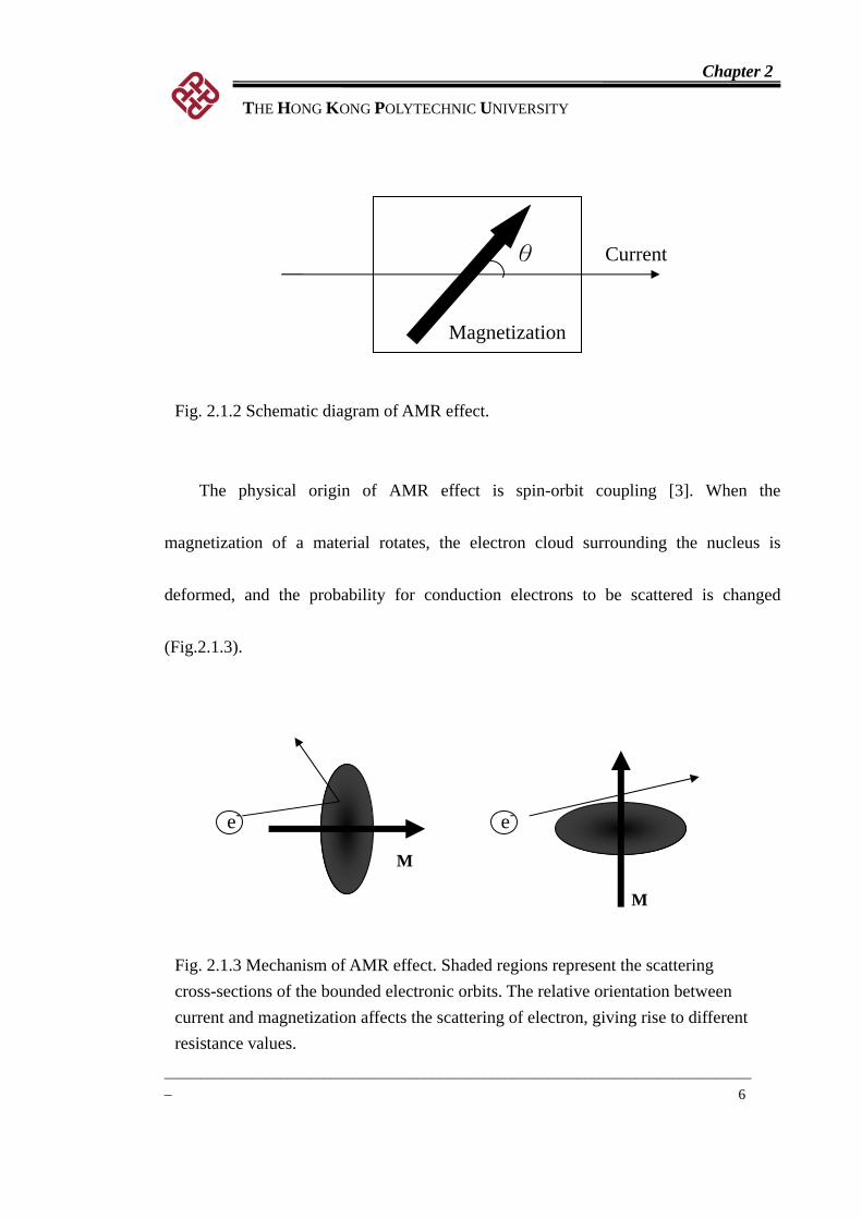
The physical origin of AMR effect is spin-orbit coupling [3]. When the
magnetization of a material rotates, the electron cloud surrounding the nucleus is
defor
Fig. 2.1.3 Mechanism of AMR effect. Shaded regions represent the scattering cross-sections of the bounded electronic orbits. The relative orientation between current and magnetization affects the scattering of electron, giving rise to different resistance values.
med, and the probability for conduction electrons to be scattered is changed
(Fig.2.1.3).
e- e-
M
M
θ Current
Magnetization
Fig. 2.1.2 Schematic diagram of AMR effect.
Chapter 2
THE HONG KONG POLYTECHNIC UNIVERSITY
__________________________________________________________________________________
7
The effect was previously used in magnetic read heads applications [3], with NiFe
(permalloy) being commonly used due to its moderate MR (~5%) at low magnetic fields
and at room temperature.
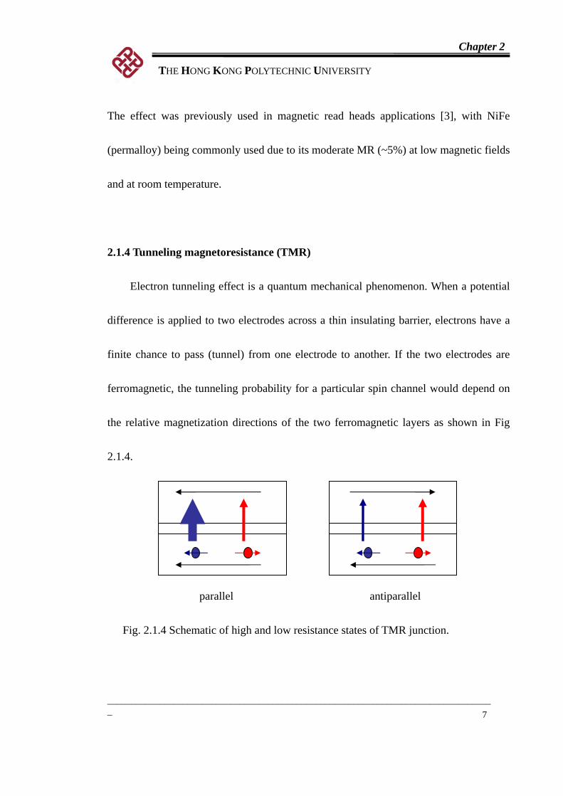
2.1.4 Tunneling magnetoresistance (TMR)
Electron tunneling effect is a quantum mechanical phenomenon. When a pot
ifference is applied
ential
d to two electrodes across a thin insulating barrier, electrons have a
directions of the two ferromagnetic layers as shown in Fig
.1.4.
finite chance to pass (tunnel) from one electrode to another. If the two electrodes are
ferromagnetic, the tunneling probability for a particular spin channel would depend on
the relative magnetization
2
Fig. 2.1.4 Schematic of high and low resistance states of TMR junction.
parallel antiparallel
Chapter 2
THE HONG KONG POLYTECHNIC UNIVERSITY
__________________________________________________________________________________
8
The dissimilar tunneling conductances arise from the asymmetry of spin sub-bands,
which is the origin of the TMR effect. TMR ratio is defined as
p
pAP
RRR
TMR−
= (2.1.5)
where and are resistances with the ferromagnetic layers in anti-parallel and
parallel configurations, respectively.
t was not
reproduced until 1995, when a TMR ratio of ~12% at room temperature was reported in
s been reached at room
temperature in CoFeB\MgO\CoFeB system [6].
2.1.5 Colossal magnetoresistance (CMR)
In mixed-valence manganites with perovskite structures, a large MR effect was
discovered when the material was exposed to a high magnetic field (127000% at 77K,
under a 6 Tesla field for La0.67Ca0.33MnO3 thin films) [7]. Similarly large MR effect was
also observed in complex oxides such as double perovskites and layered perovskites [8].
Because of the very large MR effect, and to distinguish it from the GMR effect, it is
apR pR
TMR was first observed in Fe\Ge\Co junctions in 1975 [4], but the effec
CoFe\Al2O3\Co junctions [5]. Nowadays, TMR performances of tunnel junctions have
been greatly improved, and a large MR ratio of ~230% ha
Chapter 2
THE HONG KONG POLYTECHNIC UNIVERSITY
__________________________________________________________________________________
9
called CMR. The origin of the CMR effect will be further discussed in Section 2.2.
2.1.6 Giant magnetoresistance
2.1.6.1 Introduction
The GMR effect was discovered in 1988 in Fe/Cr metallic multilayers [9]. A large
MR ratio up to 80%, with Hs ~ 20 kOe, at 4.2K, was reported. The effect originated
from changes in the relative magnetization orientations of magnetic layers. The GMR
ratio is defined basically in the same way as TMR:
↑↑
↑↑↑↓ −=RR
GMR (2.1.4) R
where and are the resistances of the sample, when the magnetization of the
layers are in parallel and anti-parallel configurations, respectively.
The resistance of GMR structure depends on the magnetization directions of
magnetic layers. In multilayered structures, magnetic layers are separated by very thin
non-magnetic layers (spacer layers), in the order of Å. If a magnetic field is applied on
the sample, the magnetization of layers can be switched independently. For simplicity,
suppose the magnetization of layers can be oriented in only two extreme configurations
(parallel and anti-parallel magnetization alignments) as shown in Fig. 2.1.5. Such a
↑↑R ↑↓R
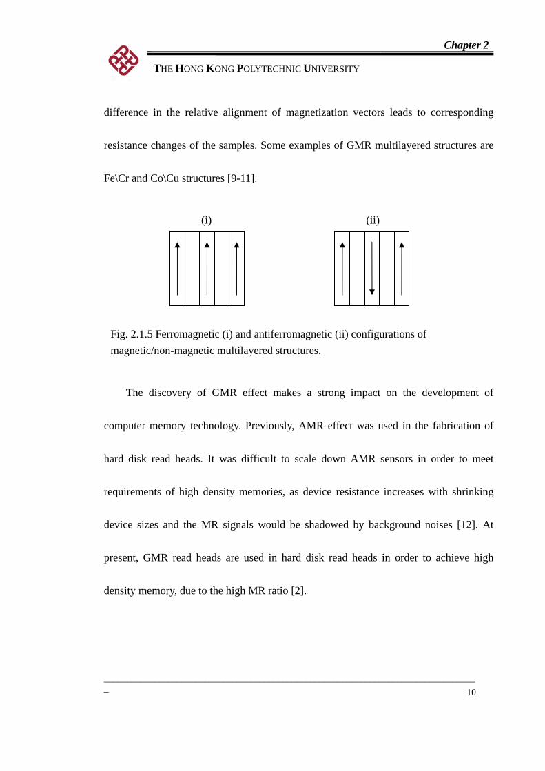
Chapter 2
THE HONG KONG POLYTECHNIC UNIVERSITY
__________________________________________________________________________________
10
difference in the relative alignment of magnetization vectors leads to corresponding
resistance changes of the samples. Some examples of GMR multilayered structures are
Fe\C
The discovery of GMR effect makes a strong impact on the development of
computer memory technology. Previously, AMR effect was used in the fabrication of
hard disk read heads. It was difficult to scale down AMR sensors in order to meet
ncreases with shrinking
device sizes and the MR signals would be shadowed by background noises [12]. At
present, GMR read heads are used in hard disk read heads in order to achieve high
d
r and Co\Cu structures [9-11].
Fig. 2.1.5 Ferromagnetic (i) and antiferromagnetic (ii) configurations of magnetic/non-magnetic multilayered structures.
(i) (ii)
requirements of high density memories, as device resistance i
ensity memory, due to the high MR ratio [2].
Chapter 2
THE HONG KONG POLYTECHNIC UNIVERSITY
__________________________________________________________________________________
11
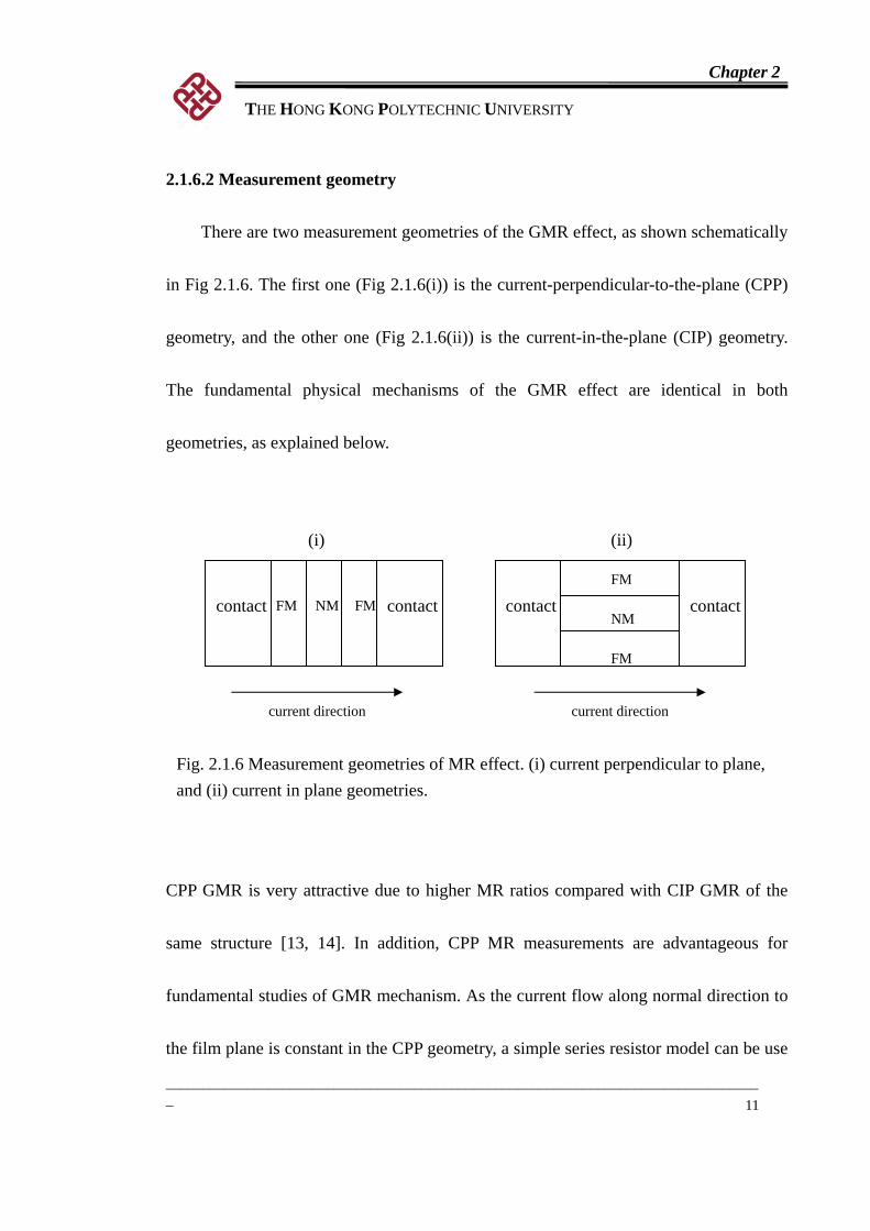
2.1.6.2 Measurement geometry
There are two measurement geometries of the GMR effect, as shown schematically
in Fig 2.1.6. The first one (Fig 2.1.6(i)) is the current-perpendicular-to-the-plane (CPP)
geometry, and the other one (Fig 2.1.6(ii)) is the current-in-the-plane (CIP) geometry.
The fundamental physical mechanisms of the GMR effect are identical in both
geometries, as explained below.
CPP GMR is very attractive due to higher MR ratios compared with CIP GMR of the
same structure [13, 14]. In addition, CPP MR measurements are advantageous for
fundamental studies of GMR mechanism. As the current flow along normal direction to
the film plane is constant in the CPP geometry, a simple series resistor model can be use
contact coFM NM FM ntact contact contact FM
NM
and (ii) current in plane geometries.
(ii) (i)
FM
current direction current direction
Fig. 2.1.6 Measurement geometries of MR effect. (i) current perpendicular to plane,
Chapter 2
THE HONG KONG POLYTECHNIC UNIVERSITY
__________________________________________________________________________________
12
for analysis. In CIP geometry, on the other hand, the current density depends heavily on
the resistance of individual layers, as well as electrode and sample geometries. CIP MR
data are thus more difficult for quantitative analysis.
2.1.6.3 Origin of GMR
a two-current model proposed by Mott [15]. He
suggested that electrical conductivity in metals can be separated into two conduction
Mott also pointed out that the scattering rates of up-spin and down-spin electrons
netic metals. According to Mott, electric current is carried by
elect
GMR effect can be understood by
channels, corresponding to up-spin (majority spin) and down-spin (minority spin)
electrons. When the temperature is sufficiently low (T<<Tc), the probability of
spin-reversal processes (such as scattering by magnons or magnetic impurities) is small,
as compared to other scattering processes in which spin orientations are conserved.
Therefore, the electric current is carried independently by majority and minority
electrons, and electrical conduction occurs for two separate spin channels in a parallel
circuit.
are different in ferromag
rons from s bands because of their high mobility and low effective mass. On the

Chapter 2
THE HONG KONG POLYTECHNIC UNIVERSITY
__________________________________________________________________________________
13
other hand, localized d bands provide final states for the scattering of electrons. Due to
the exchange interaction between d-band electrons in ferromagnetic metals, the majority
and minority spin bands are split and shifted with respect to each other (Fig 2.1.7).
Thus, the density of states at Fermi levels in majority and minority bands are different.
As the probability of scattering is proportional to the density of states at Fermi level, the
scattering rates are spin-dependent [15]. As a result, the resistivity of majority and
minority spin electrons are different.
Fig. 2.1.7 Schematic view of band structures of Fe, Co and Ni (i) and Cu (ii).
(i) (ii)
Chapter 2
THE HONG KONG POLYTECHNIC UNIVERSITY
__________________________________________________________________________________
14
up spin
down spin
up spin
down spin
(ii) (i)
Fig. 2.1.8 Schematic illustration of electron transport in multilayer for parallel (i) and antiparallel (ii) magnetization configurations. Cartoons at the bottom of each
Based on the arguments mentioned above, the GMR effect in magnetic multilayers
can be explained as follows. Figure 2.1.8 shows a magnetic/non-magnetic multilayered
structure in parallel and anti-parallel configurations. For the magnetization of magnetic
layers in parallel configuration (Fig 2.1.8(i)), one of the spin channels has electrons
passing through the structure with less scattering. On the other hand, the opposite spin
channel suffers more scattering. As the two spins channels do not mix strongly,
electrical conduction occurs in parallel for two different spin channels. The total
resistance of the multilayer is therefore low, due to shunting by the highly conductive
figure show the resistor networks under the two-current series resistor model [16].
Chapter 2
THE HONG KONG POLYTECHNIC UNIVERSITY
__________________________________________________________________________________
15
up-spin channel. When the magnetization of magnetic layers are in the antiparallel
configuration (Fig 2.1.8(ii)), both the up and down spin electrons suffer from strong
scattering because electrons of one spin channel (up or down) in one magnetic layer will
become members of the other channel (down or up) as they enter the next magnetic
layer. The total resistance of the multilayer is high in this case.
This scattering mechanism proposed by Mott is effective for bulk ferromagnetic
materials, and is referred as the bulk spin dependent scattering. On the other hand,
in spin
d
different band structures, a potential step can be created at the interface [17]. Thus, the
trans
terfaces between ferromagnetic and non-magnetic materials also contribute to the
ependent transport in magnetic multilayers [17]. For two adjacent materials with
mission probability across the interface layer is reduced. Because the band
structures of ferromagnetic materials are spin-dependent, the transmission across
interfaces between ferromagnetic and non magnetic layer is also spin-dependent.
Chapter 2
THE HONG KONG POLYTECHNIC UNIVERSITY
__________________________________________________________________________________
16
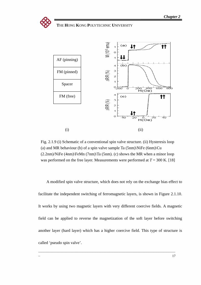
2.1.6.4 Spin valve
To achieve parallel and anti parallel configurations of the magnetic layers that can
be switched with small magnetic fields, Dieny et al. [18] fabricated a ‘spin valve’
structure as shown in Figure 2.1.9(i). In such a structure, the two ferromagnetic layers
are uncoupled from each other by using a relatively thick spacer layer (typically a few
nm). To facilitate independent switching of ferromagnetic layers, exchange bias effect
[19] was used. It was done by depositing an antiferromagnetic layer (pinning layer)
adjacent to one of the ferromagnetic layers (pinned layer) in an external magnetic field.
The magnetization of the pinned layer remains unchanged, until a large magnetic field is
applied. The other ferromagnetic layer (free layer), having a much smaller coercivity,
can then be switched with a much lower magnetic field. Figure 2.1.9(ii) shows the room
temperature hysteresis loop and MR behaviour of a typical spin valve structure [18].
Chapter 2
THE HONG KONG POLYTECHNIC UNIVERSITY
__________________________________________________________________________________
17
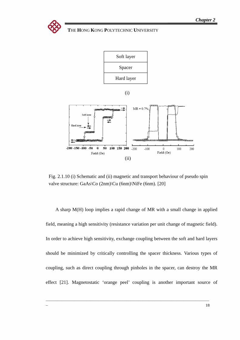
A modified spin valve structure, which does not rely on the exchange bias effect to
facilitate the independent switching of ferromagnetic layers, is shown in Figure 2.1.10.
It works by using two magnetic layers with very different coercive fields. A magnetic
field can be applied to reverse the magnetization of the soft layer before switching
another layer (hard layer) which has a higher coercive field. This type of structure is
called ‘pseudo spin valve’.
Fig. 2.1.9 (i) Schematic of a conventional spin valve structure. (ii) Hysteresis loop (a) and MR behaviour (b) of a spin valve sample Ta (5nm)\NiFe (6nm)\Cu (2.2nm)/NiFe (4nm)\FeMn (7nm)\Ta (5nm). (c) shows the MR when a minor loop was performed on the free layer. Measurements were performed at T = 300 K. [18]
AF (pinning)
FM (pinned)
Spacer
FM (free)
(i) (ii)
Chapter 2
THE HONG KONG POLYTECHNIC UNIVERSITY
__________________________________________________________________________________
18
Soft layer
Spacer
Hard layer
(i)
(ii)
o spin Fig. 2.1.10 (i) Schematic and (ii) magnetic and transport behaviour of pseudvalve structure: GaAs\Co (2nm)\Cu (6nm)\NiFe (6nm). [20]
A sharp M(H) loop implies a rapid change of MR with a small change in applied
field, meaning a high sensitivity (resistance variation per unit change of magnetic field).
In order to achieve high sensitivity, exchange coupling between the soft and hard layers
should be minimized by critically controlling the spacer thickness. Various types of
coupling, such as direct coupling through pinholes in the spacer, can destroy the MR
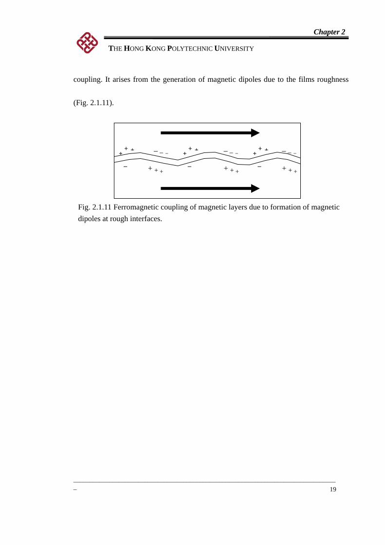
effect [21]. Magnetostatic ‘orange peel’ coupling is another important source of
Chapter 2
THE HONG KONG POLYTECHNIC UNIVERSITY
__________________________________________________________________________________
19
coupling. It arises from the generation of magnetic dipoles due to the films roughness
(Fig. 2.1.11).
Fig. 2.1.11 Ferromagnetic coupling of magnetic layers due to formation of magnetic dipoles at rough interfaces.
_ _ _ ++ + +
+ +_ _ _
+ + + _
+ + + _
_
+ + + _ _ _
+ + +

Chapter 2
THE HONG KONG POLYTECHNIC UNIVERSITY
__________________________________________________________________________________
20
2.2 Half metallic manganites
2.2.1 Introduction
rte rge increase of electrical
conductivity a the m valen e ratio of +/M incr (doping level
In 1950, Jonker and Van Santen carried out studies on the compounds
La1-xAxMnO3 (A=Ca, Sr and Ba) [22, 23]. They repo d a la
s ixed c Mn4 n3+ eased
++
+
+= 43
4
MnMn
as accompanied by a sharp in
Mnx ). At certain values of x (=0.3) ferromagnetism was observed, which
w crease in electrical conductivity.
The research field was revived in 1993, when von Helmolt et al. reported a MR
value (
)0(/ =∆ Hρρ ) of 60% at room temperature in La0.67Ba0.33MnO3 thin films
under a 7-Tesla external field [24]. In 1994, Jin et al. reported MR values up to 1000%
at 77 K in La0.67Ca0.33MnO3 thin films under a 6-Telsa field [7]. Such kind of huge
resistance changes under high magnetic fields is termed as colossal magnetoresistance
(CMR).
Chapter 2
THE HONG KONG POLYTECHNIC UNIVERSITY
__________________________________________________________________________________
21
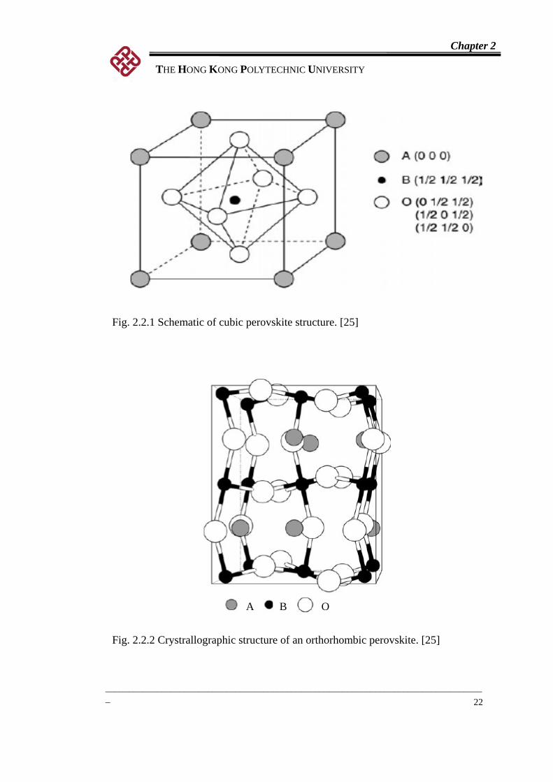
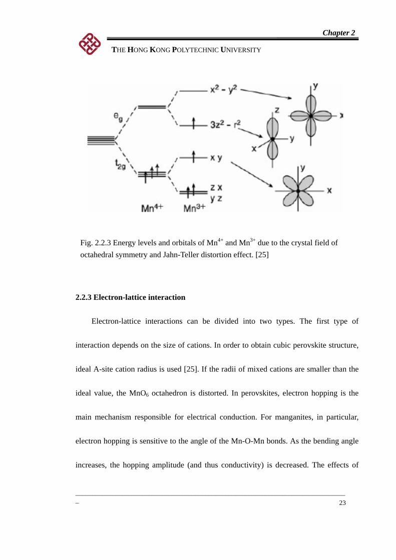
2.2.2 Crystal and electronic structures
manganites RE1−xMxMnO3 (RE = rare earths, M = Ca, Sr, Ba, Pb)
are C
maintain the cub
h will be discussed later.
Mixed valence
MR materials with perovskite crystal structure (ABO3) (Fig.2.2.1). The Mn ions
occupy the B-sites with octahedral oxygen coordination. The MnO6 octahedra share the
corners to form a three-dimensional network. As interstitial A-site ions do not fit to
ic symmetry to MnO6, it lowers the cubic symmetry and form
orthorhombic perovskites (Fig 2.2.2).
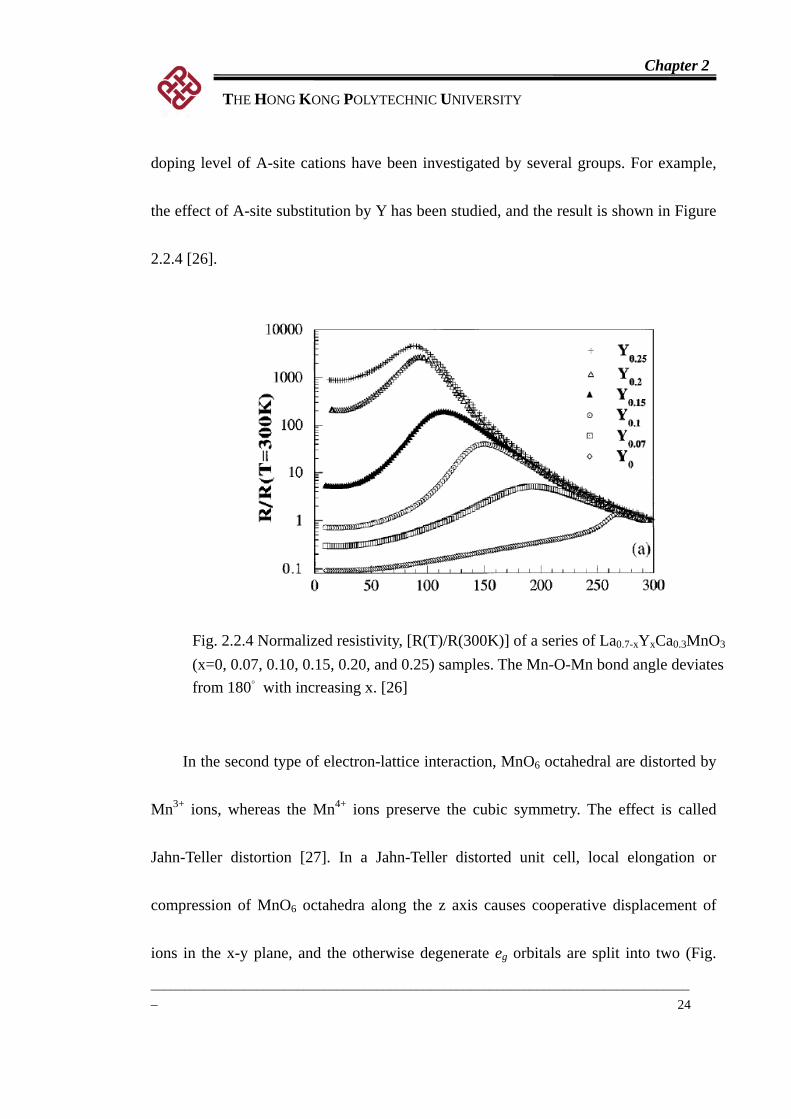
Isolated Mn ions have five degenerated 3d orbitals. In the crystal form, the 3d
orbitals are split by crystal fields and form three t2g orbitals with lower energy and two
eg orbitals with higher energy (Fig 2.2.3). For Mn3+ ions, the t2g orbitals are completely
filled and one electron fills in the eg orbital. All these electrons are aligned in parallel
due to Hund’s coupling. There is further orbital degeneracy lifting due to the Jahn-Teller
effect whic
Chapter 2
THE HONG KONG POLYTECHNIC UNIVERSITY
__________________________________________________________________________________
22
Fig. 2.2.1 Schematic of cubic perovskite structure. [25]
Fig. 2.2.2 Crystrallographic structure of an orthorhombic perovskite. [25]
A B O
Chapter 2
THE HONG KONG POLYTECHNIC UNIVERSITY
__________________________________________________________________________________
23
Fig. 2.2.3 Energy levels and orbitals of Mn4+ and Mn3+ due to the crystal field of octahedral symmetry and Jahn-Teller distortion effect. [25]
2.2.3 Electron-lattice interaction
Electron-lattice interactions can be divided into two types. The first type of
interaction depends on the size of cations. In order to obtain cubic perovskite structure,
ideal A-site cation radius is used [25]. If the radii of mixed cations are smaller than the
ideal value, the MnO6 octahedron is distorted. In perovskites, electron hopping is the
main mechanism responsible for electrical conduction. For manganites, in particular,
electron hopping is sensitive to the angle of the Mn-O-Mn bonds. As the bending angle
increases, th
fects of e hopping amplitude (and thus conductivity) is decreased. The ef
Chapter 2
THE HONG KONG POLYTECHNIC UNIVERSITY
__________________________________________________________________________________
24
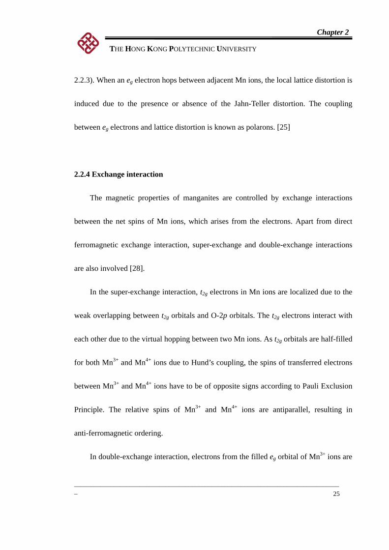
doping level of A-site cations have been investigated by several groups. For example,
the effect of A-site substitution by Y has been studied, and the result is shown in Figure
2.2.4 [26].
In the second type of electron-lattice interaction, MnO6 octahedral are distorted by
Mn3+ ions, whereas the Mn4+ ions preserve the cubic symmetry. The effect is called
Jahn-Teller distortion [27]. In a Jahn-Teller distorted unit cell, local elongation or
compression of MnO6 octahedra along the z axis causes cooperative displacement of
ions in the x-y plane, and the otherwise degenerate eg orbitals are split into two (Fig.
(x=0, 0.07, 0.10, 0.15, 0.20, and 0.25) samples. The Mn-O-Mn bond angle deviates Fig. 2.2.4 Normalized resistivity, [R(T)/R(300K)] of a series of La0.7-xYxCa0.3MnO3
from 180° with increasing x. [26]
Chapter 2
THE HONG KONG POLYTECHNIC UNIVERSITY
__________________________________________________________________________________
25
2.2.3). When an eg electron hops between adjacent Mn ions, the local lattice distortion is
induced due to the presence or absence of the Jahn-Teller distortion. The coupling
between eg electrons and lattice distortion is known as polarons. [25]
2.2.4 Exchange interaction
The magnetic properties of manganites are controlled by exchange interactions
between the net spins of Mn ions, which arises from the electrons. Apart from direct
ferromagnetic exchange interaction, super-exchange and double-exchange interactions
are also involved [28].
In the super-exchange interaction, t2g electrons in Mn ions are localized due to the
weak
each o een two Mn ions. As t2g orbitals are half-filled
for both Mn3+ and Mn4+ ions due to Hund’s coupling, the spins of transferred electrons
between Mn3+ and Mn4+ ions have to be of opposite signs according to Pauli Exclusion
Principle. The relative spins of Mn3+ and Mn4+ ions are antiparallel, resulting in
anti-ferromagnetic ordering.
In double-exchange interaction, electrons from the filled eg orbital of Mn3+ ions are
overlapping between t2g orbitals and O-2p orbitals. The t2g electrons interact with
ther due to the virtual hopping betw
Chapter 2
THE HONG KONG POLYTECHNIC UNIVERSITY
__________________________________________________________________________________
26
transferred to O-2p orbitals. At the same time, electrons from O-2p orbitals are
transferred to empty eg orbitals of Mn4+ ions. This electron transfer process strongly
depends on the t2g spin orientation in the two Mn ions. When the localized t2g spins of
two Mn ions are aligned parallel, eg electron transfer is possible with maximum kinetic
n transfer is )2
cos(0θtenergy. The probability of eg electro , where θ is the angle between
Mn
hown in Figure 2.2.5. In 3d ferromagnetic metals such as Ni,
both
ion spins and 0t is the hopping parameter [29]. Therefore, this double electron
transfer process between Mn3+ and Mn4+ ions causes ferromagnetic ordering.
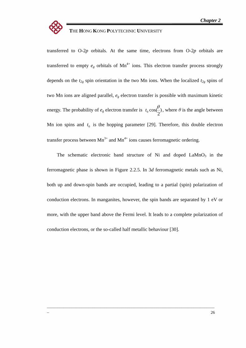
The schematic electronic band structure of Ni and doped LaMnO3 in the
ferromagnetic phase is s
up and down-spin bands are occupied, leading to a partial (spin) polarization of
conduction electrons. In manganites, however, the spin bands are separated by 1 eV or
more, with the upper band above the Fermi level. It leads to a complete polarization of
conduction electrons, or the so-called half metallic behaviour [30].
Chapter 2
THE HONG KONG POLYTECHNIC UNIVERSITY
__________________________________________________________________________________
27
2.3 Summary
This chapter introduced different types of magnetoresistances including ordinary
MR, anisotropic MR, tunneling MR, colossal MR and giant MR. The concepts of half
metallic manganites were also introduced as the background to understand the
experimental work presented in Chapters 4 and 5.
Fig. 2.2.5 Schematic view of band structures of Ni and LSMO [25].
La0.7Sr0.3MnO3Ni
Chapter 3
THE HONG KONG POLYTECHNIC UNIVERSITY
__________________________________________________________________________________
28
CHAPTER 3
Experimental Methods
3.1 Pulsed laser deposition (PLD)
3.1.1 Introduction
After Dijkkamp first used the technique to prepare high temperature
superconducting films in 1987 [31], PLD technique has gained tremendous interest and
emerged as a versatile method to obtain epitaxial thin films of multi-component oxides.
Various classes of materials, including ferroelectrics [32], ferromagnets [33] and
dielectric oxides, have been grown successfully by the method, either as single layers or
in multilayer form.
The basic principle of PLD is described as follows. Laser pulses are focused by
converging lens. The pulses enter a vacuum chamber through a window and impinge on
the target material. To ensure that only the surface layer of the ablated target is being
heated up, laser pulses with energy density of a few Jcm-2 and short duration (~20 ns)
are generally used. As thermal conduction cannot set in for such a short time scale, all of
the absorbed energy is confined at the surface layer of the target. A few thousand
Chapter 3
THE HONG KONG POLYTECHNIC UNIVERSITY
__________________________________________________________________________________
29
degrees Celsius can be achieved at the surface of the target [34].
3.1.2 Mechanism of PLD
The PLD process can be divided into four stages: (1) laser-target interaction, (2)
dynamics of the ablated materials, (3) deposition of ablated materials on the substrate,
and (4) nucleation and film growth.
In the first stage, focused laser pulses impinge on the target. All elements on the
target surface are rapidly evaporated, and are ablated with identical stoichiometry as
target material. The ablation process has a number of physical origins, including thermal,
electronic, exfoliational and hydrodynamic. Thermal sputtering is the vaporization from
a momentarily heated target. Electronic sputtering involves some forms of excitation or
ionization such as production of electron-hole pairs, transition to anti-bonding potential
energy on surface, lattice-localized relaxation and desorption from the surface.
Exfoliation is the flake detachment from the target owing to repeated thermal shocks.
Finally, droplets of materials can be formed and expelled from a target due to
momentary melting [34].
In the second stage, ablated materials move towards the substrate according to laws
Chapter 3
THE HONG KONG POLYTECHNIC UNIVERSITY
__________________________________________________________________________________
30
of fluid dynamics. The moving front of such a collection of particles form a luminous
plasma called plume. The profile of the plume is described by a cosnθ curve, where
n>>1 [35].
In the third stage, ablated high-energy species impinge onto the substrate surface
and sputter some of the surface atoms away. A collision region is established between
sputtered atoms from the substrate and incoming energetic species. This collision region
serves as a source for the condensation of atoms. Films start growing at a time after the
region is formed.
In the final stage, nucleation and growth of crystalline films occur. The process
depends on several factors such as density and energy of ablated species, their degrees
of ionization, substrate temperature, and physical-chemical processes occurring on the
substrates. The nucleation and growth of films can be categorized into three different
modes: (1) three-dimensional island growth (Volmer-Weber), (2) two-dimensional
full-mono-layer growth (Frank-van der Merwe), and (3) two-dimensional growth of full
monolayers followed by the nucleation and growth of three-dimensional islands
(Stransk-Kastinov) [34].
Chapter 3
THE HONG KONG POLYTECHNIC UNIVERSITY
__________________________________________________________________________________
31
3.1.3 Advantages of PLD
Films fabricated by PLD normally retain the stoichiometry of multicomponent
targets, as long as there are no volatile species involved. It is due to the very high energy
density of the focused laser pulses. Such energetic pulses can evaporate all the
components in the target at the same time in spite of their different activation energies.
In addition, the energetic species have sufficient kinetic energies to migrate to their
favorable sites after landing on the substrates, which is further assisted by the high
substrate temperatures. By using a rotating multi-target holder with suitable optical
alignment, in situ growth of different materials under different ambient gas conditions is
feasible.
3.1.4 Disadvantage of PLD
Some shortcomings for thin film deposition using PLD have been identified. There
are two main problems: (1) inhomogenity of film thickness across the same sample, and
(2) generation of particulates.
For a typical PLD system setup, due to the angular spread of the plume, reliable
thickness calibrations can only be obtained around an area of 1 cm2 directly under the
Chapter 3
THE HONG KONG POLYTECHNIC UNIVERSITY
__________________________________________________________________________________
32
plume. Even so, the films are generally thicker right under the centre of the plasma
plume, and the film thickness decreases with increasing distance from the plume center.
The uniformity of film thickness can be improved by rotating the substrates during
deposition [34].
Generation of particulates is also a common problem in PLD. The size of
particulates can be as large as a few microns. The presence of particulates can greatly
affect the growth of subsequent layers, and can jeopardize the usefulness of the films,
especially in microelectronics applications [36]. To reduce the amount of particulates
formed, a blocking mask can be placed in between the substrate and the target holder
[34].
3.1.5 PLD setup
Figure 3.1 shows the configuration of the PLD system used in this project. In this
PLD system, laser pulses were provided by a KrF Lambda Physik COMPex 200
excimer laser with wavelength 248 nm. Laser pulses (~20 ns) with energy in the range
of 150 – 600 mJ could be produced by the laser. The cross sectional area of the beam
was 1 cm × 3 cm as it left the laser. The maximum pulse repetition rate used for PLD
Chapter 3
THE HONG KONG POLYTECHNIC UNIVERSITY
__________________________________________________________________________________
33
was 20 Hz. Laser-quality optical “UV-grade fused silica” windows and lenses were used
in the PLD system, with a transmittance over 90 % for the wavelength range from 185
to 2000 nm. A focusing lens was used to achieve high laser fluence (~ 5 Jcm-2) for target
ablation. The focal length of the lens was 30 cm, matching the size of the chamber. To
increase the flexibility of the PLD setup, two deposition chambers were installed served
by the same excimer laser. The laser source was decoupled from the deposition
chambers, and a beam steering mirror was used to direct the laser beam to either one of
the two deposition chambers. To minimize propagation losses, multi-layered dielectric
narrow-band high-reflection mirrors were used, with a reflectivity higher than 95 % at
the wavelength 248 nm.

Chapter 3
THE HONG KONG POLYTECHNIC UNIVERSITY
__________________________________________________________________________________
34
The PLD chamber used in this project consisted of the following components: 2
deposition chamber, target manipulator, substrate holder and heater, vacuum pump, gas
supply and vacuum gauges. All vacuum chambers had ports for vacuum pumping,
pressure gauging, targets, substrates, laser beam and viewports. One of the chambers
was used for oxide film deposition, which was connected to a rotary pump. A gas inlet
port was used for the afflux of oxygen (99.7 % purity), which provided an oxygen
environment for oxide thin film fabrication. The chamber was pumped down to a base
pressure of 1 mTorr. Afterwards, oxygen was filled into the chamber to the desired film
Fig. 3.1 Schematic diagram of a PLD system used in the project.
Laser beam
Window
Fused silica
Substrate holder
Window
Target
holder
Target
Beam steering
mirror
Excimer laser
Fused silica
Focusing
lens
Gas inlet
Substrate holder
Window
Target
holder
Target
Chamber with rotary pump
Chamber with rotary pump and
diffusion pump
Chapter 3
THE HONG KONG POLYTECHNIC UNIVERSITY
__________________________________________________________________________________
35
growth pressure. For metal film deposition, better vacuum deposition conditions were
needed. In such a case, another chamber with diffusion pump was used to achieve the
base pressure of 10-6 Torr.
To control the substrate temperature during film deposition process, a home-made
substrate holder with diameter of 4 cm was used. It provided a stable substrate
temperature up to 700 °C. Halogen quartz lamps, enclosed in a cylindrical stainless steel
case, were used as heating elements. A type-K thermocouple was used for registering
the temperature on the substrate holder, and the heating rate was controlled by a
programmable controller. The substrates were mounted on the substrate holder with
high temperature-compatible silver paste. Due to the high thermal conductivity of silver
paste, a uniform temperature distribution across the substrates could be achieved.
3.2 Characterization and measurements
3.2.1 Structural characterization
3.2.1.1 X-ray diffractometry (XRD)
XRD is a non-destructive method for characterizing crystal structures of materials.
When a x-ray beam interacts with the atoms in the material, the beam is diffracted.
Chapter 3
THE HONG KONG POLYTECHNIC UNIVERSITY
__________________________________________________________________________________
36
Based on Bragg’s law, diffracted beams constructively interfere only if they are at
certain incident angles with the crystal planes. The Bragg condition,
λθ nd =sin2 , (3.1)
shows the relation between x-rays wavelength λ, atomic plane separation d and the
angle of incident beam θ, and n is an integer. That means each material produces a
unique profile of x-ray intensity versus diffracted angle. From the diffraction pattern, we
can determine the phases present in the sample, as well as crystallographic information,
by comparing the XRD pattern to a library of known diffraction patterns.
An x-ray diffractometer consists of an x-ray source, slits of varying widths, a
monochromator and a detector. X-ray is obtained by accelerating electrons to collide
with a target (which was made of copper, for the system used in this project). Two
relatively high-intensity radiations are emitted during the process: Kα and Kβ. The
average wavelength of the Cu Kα lines is 1.54 Å, and that of the Cu Kβ lines is 1.39 Å.
For obtaining a monochromatic x-ray beam, Ni foil was used to filter out the
characteristic Cu Kβ radiation, so that the peaks due to Cu Kβ radiations were absent
from the scans.
In the experimental geometry, there are four rotating axes of θ(ω), 2θ, χ and φ for
Chapter 3
THE HONG KONG POLYTECHNIC UNIVERSITY
__________________________________________________________________________________
37
different scan modes (Fig. 3.2), as discussed below:
Fig. 3.2 Experimental geometry showing the four primary axes of a goniometer, the x-ray tube, detector and slits. [37]
• In a θ-2θ scan, the x-ray source is fixed, and the sample is rotated about an axis (ω
-axis) that is normal to the plane containing the x-ray beam and the detector. The
detector is rotated at twice the angular speed of the sample rotation, and the
strongest signals is received for zeroth order (n=1) diffraction. θ-2θ scans can be
used to determine the out-of-plane lattice parameters, and hence the crystalline
phases present in the film and their crystallographic orientations.
• In a ω-scan, the x-ray and the detector are fixed, and the sample is rocked about the
Chapter 3
THE HONG KONG POLYTECHNIC UNIVERSITY
__________________________________________________________________________________
38
ω-axis. The value of the full width at half maximum (FWHM) of the rocking curve
reflects the degree of alignment among crystalline grains in the sample. Generally, a
FWHM of around 1° is considered to be highly-oriented.
In a φ-scan, the source and the detector are fixed at 2θ values corresponding to a •
ucture as an example, if the epitaxial relation of a thin film with
specific atomic plane separation of the crystal structure. The sample is then tilted to
a certain angle through the χ axis depending on the crystal structure. The sample is
rotated about the φ axis that is normal to the sample stage. The φ scan can be used to
determine the in-plane crystal structure, and the epitaxial relation between the film
and the substrate.
Using the cubic str
cubic structure (with (100) out-of-plane orientation) is to be determined, the family
of (100) planes of the film and the substrate should be selected for investigation. If
the film is rotated by 45° through the χ axis (that is the line passing through the
x-ray beam, sample stage and the detector), (101) planes diffractions can be
obtained in θ-2θ scan. As the cubic structure has a four-fold symmetry in (101)
planes, four peaks of (101), (101), (101), and (101) planes separated by 90° can be
observed in a 360° φ scan. If he fou peaks of the film match to the peak positions t r
Chapter 3
THE HONG KONG POLYTECHNIC UNIVERSITY
__________________________________________________________________________________
39
of the substrate, it can be concluded that the film is epitaxially grown, cube-on-cube,
on the substrate.
.2.1.2 Transmission electron microscopy (TEM)
L 2010 system. The system used a
aB
lling. Firstly,
3
TEM analyses were performed by using a JEO
L 6 electron source, and the electrons from the source were accelerated to 200 keV.
Electrons were transmitted though an extremely thin specimen to form a diffraction
image. The maximum magnification of the machine was 1.5 million times.
The TEM specimens were prepared by mechanical grinding and ion mi
thin film samples were cut into two small rectangular pieces of 3×3 mm2. Two film
surfaces were stuck together, face to face, by means of G-1 epoxy. The specimen was
then grinded mechanically to around 1 mm in thickness by using a series of abrasive
papers with particle size ranging from 100 µm down to 20 µm. The grinded surface was
then polished by using diamond polishing films with particle sizes of 6 µm, 3 µm, and 1
µm. After polishing one side of the specimen, the polished side was stuck on a 3 mm
diameter copper supporting grid. The other side was then polished with the same
procedures, until the silicon substrate turned red under an optical microscope operating
Chapter 3
THE HONG KONG POLYTECHNIC UNIVERSITY
__________________________________________________________________________________
40
in the transmission mode. This indicated the thickness of the sample was around a few
microns. The thickness of the specimen was further reduced by using Ar ion milling. A
Gatan PIPS machine was used and operated at 4 kV. The specimen was milled until a
hole was formed at the sample. The beam energy was then reduced to 2 kV to minimize
the amorphous structures induced by high energy Ar ion bombardment.
3.2.1.3 Atomic force microscopy (AFM)
samples were studied by AFM operating in The surface morphology of thin film
tapping mode. The technique gives detailed information about properties such as surface
roughness and average grain size of the films. The working principle of AFM is based
on the inter-atomic forces between the tip and the atoms in the sample. The schematic
diagram of an AFM is shown in Figure 3.3.
Chapter 3
THE HONG KONG POLYTECHNIC UNIVERSITY
__________________________________________________________________________________
41
Detector and Feedback electronics Laser diode
Photodiode
Cantilever and Tip Sample surface
PZT scanner
Fig. 3.3 Schematic diagram of an AFM.
The tip is tapped over near, but not touching, the surface of a film at the
cantilever’s resonance frequency. Due to the attractive inter-atomic forces between the
tip and the film surface, some energy is lost to the surface, and the amplitude of
oscillation is reduced. When the tip is high, the oscillation amplitude becomes large, and
vice versa. A feedback loop constantly adjusts the separation between the tip and the
sample. As the typical spring constant for cantilever is about 1 N/m, a deflection as
small as 1 nm can be sensed when the force as low as 10-9 N is present between the film
and the tip. Such a small deflection can be measured by the shift of the laser beam
Chapter 3
THE HONG KONG POLYTECHNIC UNIVERSITY
__________________________________________________________________________________
42
image reflected off a shiny surface on the back of the cantilever. Nanoscale movement
of the scanner is made by a piezoelectric scanner. Vibration isolation table is equipped
to minimize the noise induced from the surrounding.
3.2.2 Magnetic measurements
s the relation between magnetic flux density (B),
agn
The follow equation show
m etic field intensity (H) and magnetization (M).
)(0 MHB += µ (3.2)
When a known external field H is applied to a v lux ibrating sample, the change of f
density B inside the sample can arise from the change in magnetization. As the sample
is vibrated, B inside the sample will generate an induced voltage in the pick-up coils
according to Faraday’s law,
)(∫ ⋅∂∂
=−= dSBtdt
dΦε (3.3)
where Φ is the flux through the coils and dS is an elemen
LakeShore
mod
t of vector area.
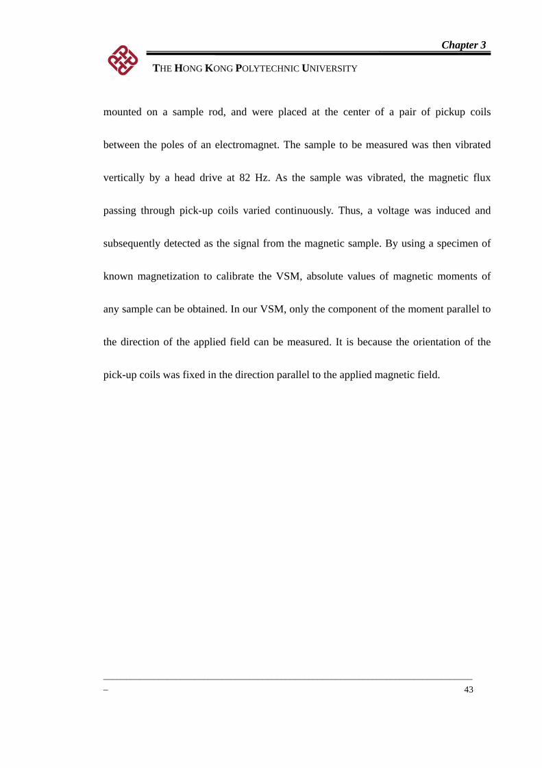
The magnetic properties of the samples were measurement by using a
el 7407 vibrating sample magnetometer (VSM) system. Figure 3.4 shows the
schematic diagram of a VSM system. For the system used in this project, samples were
Chapter 3
THE HONG KONG POLYTECHNIC UNIVERSITY
__________________________________________________________________________________
43
mounted on a sample rod, and were placed at the center of a pair of pickup coils
between the poles of an electromagnet. The sample to be measured was then vibrated
vertically by a head drive at 82 Hz. As the sample was vibrated, the magnetic flux
passing through pick-up coils varied continuously. Thus, a voltage was induced and
subsequently detected as the signal from the magnetic sample. By using a specimen of
known magnetization to calibrate the VSM, absolute values of magnetic moments of
any sample can be obtained. In our VSM, only the component of the moment parallel to
the direction of the applied field can be measured. It is because the orientation of the
pick-up coils was fixed in the direction parallel to the applied magnetic field.
Chapter 3
THE HONG KONG POLYTECHNIC UNIVERSITY
__________________________________________________________________________________
44
Magnetic coils
Sample rod
Sample
Pick-up coils
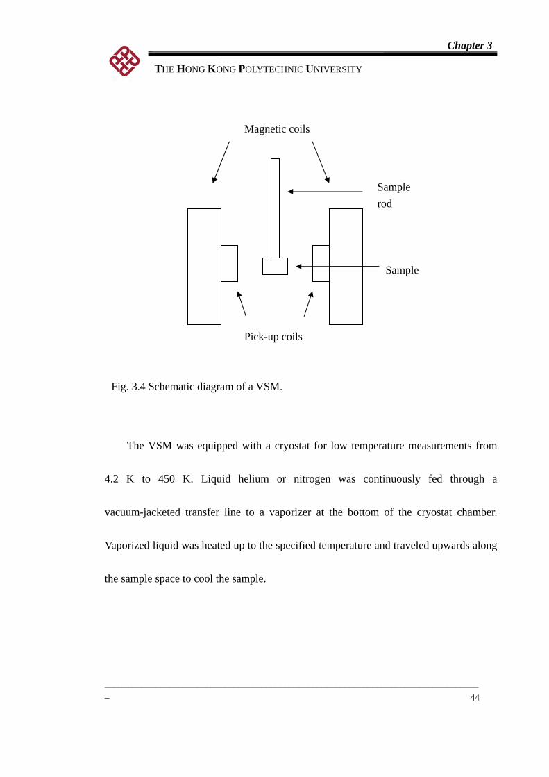
Fig. 3.4 Schematic diagram of a VSM.
The VSM was equipped with a cryostat for low temperature measurements from
4.2 K to 450 K. Liquid helium or nitrogen was continuously fed through a
vacuum-jacketed transfer line to a vaporizer at the bottom of the cryostat chamber.
Vaporized liquid was heated up to the specified temperature and traveled upwards along
the sample space to cool the sample.
Chapter 3
THE HONG KONG POLYTECHNIC UNIVERSITY
__________________________________________________________________________________
45
3.2.3 Electrical transport measurements
3.2.3.1 Resistance against temperature measurement
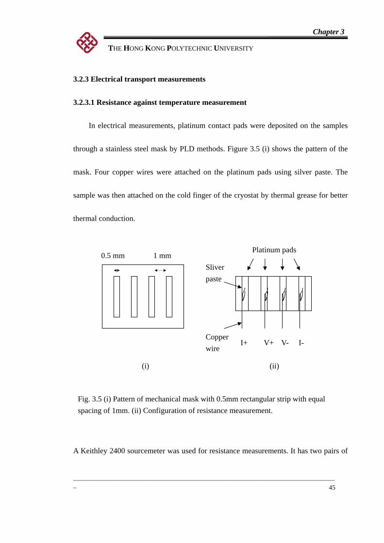
In electrical measurements, platinum contact pads were deposited on the samples
through a stainless steel mask by PLD methods. Figure 3.5 (i) shows the pattern of the
mask. Four copper wires were attached on the platinum pads using silver paste. The
sample was then attached on the cold finger of the cryostat by thermal grease for better
thermal conduction.
Platinum pads 0.5 mm 1 mm
Sliver paste
Copper wire
I+ V+ V- I-
(i) (ii)
Fig. 3.5 (i) Pattern of mechanical mask with 0.5mm rectangular strip with equal spacing of 1mm. (ii) Configuration of resistance measurement.
A Keithley 2400 sourcemeter was used for resistance measurements. It has two pairs of
Chapter 3
THE HONG KONG POLYTECHNIC UNIVERSITY
__________________________________________________________________________________
46
terminals for four point resistance measurements. By using four point measurements,
the issue of contact resistance was minimized. Figure 3.5(ii) shows the configuration for
such measurements. The measured resistance R was used to calculate the resistivity ρ
by using the Equation 3.4,
lRA
=ρ (3.4)
where l is the distance between the current contacts and A is the cross sectional area that
the current flows through.
A closed-cycle refrigerator was used to cool the sample to desired temperatures.
Samples were cooled by a cold finger through direct thermal contact. A temperature
controller was used to measure the temperature of the cold finger and to regulate the
heater, maintaining the cold finger at the desired temperature. The temperature can be
varied between 10 K to 400 K. Both the temperature controller and the sourcemeter
were operated through a LabView program. The data were taken through the computer,
and the graph of resistance against temperature (RT) was obtained.
Chapter 3
THE HONG KONG POLYTECHNIC UNIVERSITY
__________________________________________________________________________________
47
3.2.3.2 Current against voltage
Current against voltage (IV) measurements were also done by Keithley 2400
sourcemeter. The configuration of measurement was the same as Figure 3.5 (ii). The
whole measurement setup was computer controlled by a LabView program.
3.2.3.3 Resistance against magnetic field
Magnetoresistance measurements were measured in a system built in-house. The
magnetoresistance measurement setup consisted of five parts: (1) electrical circuit (with
sourcemeters and the sample), (2) an electromagnet, (3) a gaussmeter, (4) a closed-cycle
cryostat and (5) a temperature controller. The schematic diagram of the MR setup is
shown in Fig.3.6.

Chapter 3
THE HONG KONG POLYTECHNIC UNIVERSITY
__________________________________________________________________________________
48
Due to the limited space of the cryostat, the maximum size of the sample that could be
accommodated was 3 mm × 3 mm. The sample was mounted on a printed circuit board
(PCB), and four aluminum wires were bonded between the sample and the PCB by
ultrasonic wire bonding. The PCB was then mounted on a hollow copper rod with four
copper wires inside for electrical connection. The sample rod was inserted into the
cryostat between the poles of the electromagnet. The chamber and the vacuum jacket
were evacuated by a rotary pump for 30 minutes. Then, helium gas was filled into the
chamber for thermal conduction. The temperature controller was used for regulating the
I+ I- V+ V-
Electromagnet Copper rod
Sample
Cryostat Gaussmeter
Fig. 3.6 Schematic diagram of the MR setup used in the project.
Chapter 3
THE HONG KONG POLYTECHNIC UNIVERSITY
__________________________________________________________________________________
49
temperature inside the chamber from 10 K to room temperature. The electromagnet
provided a variable magnetic field up to 5000 Oe, which was measured by a gaussmeter
adjacent to the cryostat. The resistance of the sample was measured by using four point
measurement technique. All instruments were computer controlled by a LabView
program.
Chapter 4
THE HONG KONG POLYTECHNIC UNIVERSITY
__________________________________________________________________________________
50
CHAPTER 4
Effect of Post Annealing on La0.7Sr0.3MnO3 Thin Films
4.1 Introduction
Doped perovskite manganites such as La0.7Sr0.3MnO3 (LSMO) are heavily studied
for spintronics applications, due to their high spin polarization and, particularly in
LSMO, relatively high Curie temperature (TC > 370 K) [38]. According to the double
exchange theory [29, 28], ferromagnetic and metallic properties of perovskite
manganites are inter-related through the interaction between pairs of Mn3+ and Mn4+
ions. Because the ratio of Mn3+ and Mn4+ ions can be altered by oxygen content, TC of
LSMO films can be modified by controlling oxygen pressure during the deposition
process [39].
In multilayer fabrication processes, different growth conditions may be required
for the deposition of individual layers. Chemical stability of the layers has to be
carefully studied, ensuring that desired properties of individual layers are retained. For
example, Dho and Hur [39] showed that LSMO films deposited at different oxygen
pressures (varied from 250 mTorr to 450 mTorr) and annealed at 500 mTorr possessed
Chapter 4
THE HONG KONG POLYTECHNIC UNIVERSITY
__________________________________________________________________________________
51
induced lattice strain. Sun et al. [40] showed that the transport behaviour of LSMO
films strongly depended on the oxygen stoichiometry; their results showed that oxygen
vacancies in LSMO films could induce scattering and affected the resistances of
samples. Du et al. [41] reported that high temperature annealing of LSMO films at
950 °C in flowing oxygen at atmospheric pressure (deposited at 800 °C) could increase
TC and saturation magnetization of the films, and coercivity of the films was reduced at
the same time. It should be noted that these works concentrated on oxygen-deficient
LSMO films annealed in situ under high oxygen pressures and temperatures.
On the other hand, there are situations in which ex situ annealing of films are
necessary. For example, mechanical masks are occasionally used to deposit films of
specific geometries. In the absence of in situ loading mechanisms, the films need to be
cooled down to room temperature and exposed to air for placing the mask into the
chamber. As mentioned before, the oxygen content of LSMO films strongly depends on
annealing conditions, so the film properties can be changed during the process.
In this work, I investigated the effect of post annealing on the properties of LSMO
films, focusing on the effects of in situ and ex situ annealing processes under oxygen
pressures different from deposition pressures. For in situ annealing experiments, films
Chapter 4
THE HONG KONG POLYTECHNIC UNIVERSITY
__________________________________________________________________________________
52
were deposited at desired oxygen pressures and subsequently annealed. For the case of
ex situ annealing, films were first deposited at desired oxygen pressures and cooled
down to room temperature subsequently. Afterwards, the films were heated up again and
maintained at an oxygen pressure different from that used for the deposition process.
Results obtained in this chapter provide useful guidelines for the epitaxial multilayer
deposition and annealing processes.
Chapter 4
THE HONG KONG POLYTECHNIC UNIVERSITY
__________________________________________________________________________________
53
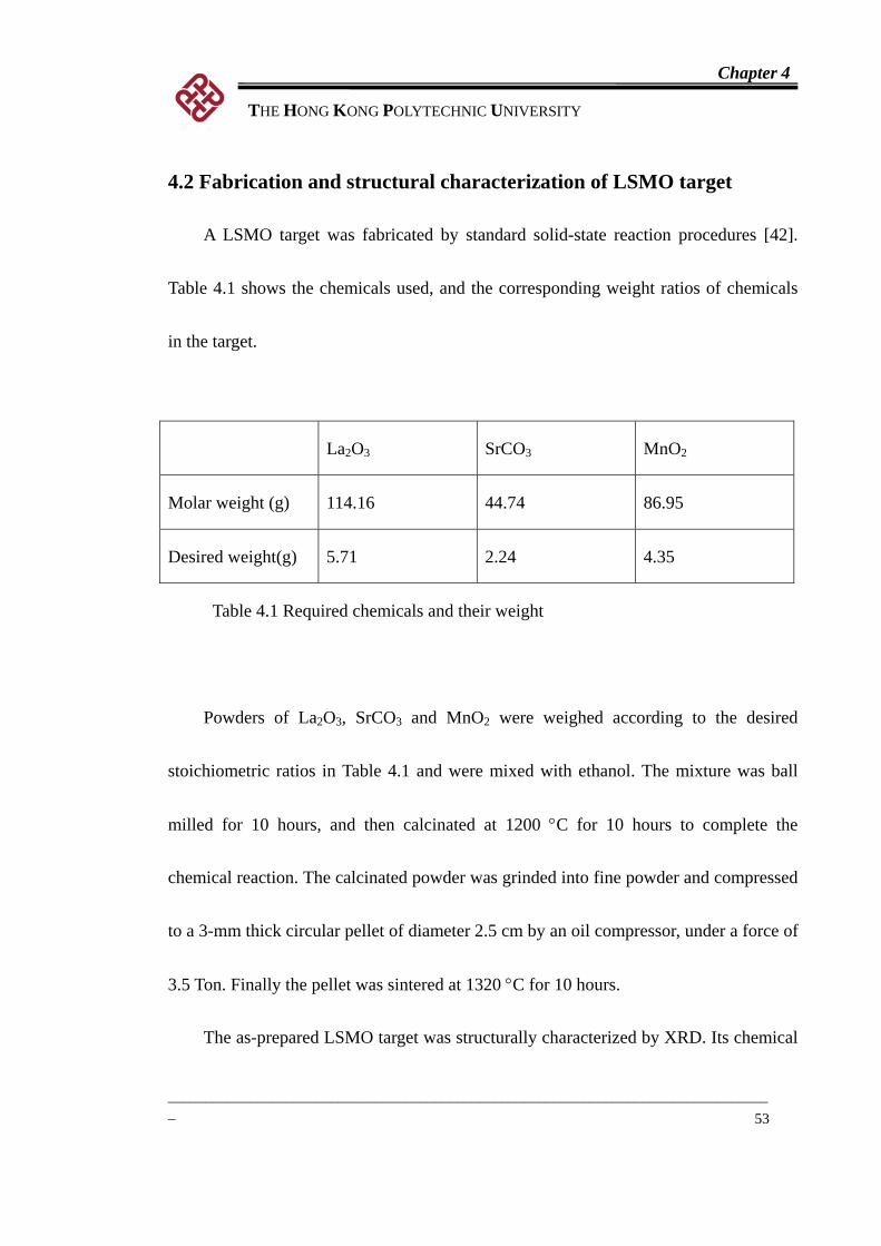
4.2 Fabrication and structural characterization of LSMO target
A LSMO target was fabricated by standard solid-state reaction procedures [42].
Table 4.1 shows the chemicals used, and the corresponding weight ratios of chemicals
in the target.
La2O3 SrCO3 MnO2
Molar weight (g) 114.16 44.74 86.95
Desired weight(g) 5.71 2.24 4.35
Table 4.1 Required chemicals and their weight
Powders of La2O3, SrCO3 and MnO2 were weighed according to the desired
stoichiometric ratios in Table 4.1 and were mixed with ethanol. The mixture was ball
milled for 10 hours, and then calcinated at 1200 °C for 10 hours to complete the
chemical reaction. The calcinated powder was grinded into fine powder and compressed
to a 3-mm thick circular pellet of diameter 2.5 cm by an oil compressor, under a force of
3.5 Ton. Finally the pellet was sintered at 1320 °C for 10 hours.
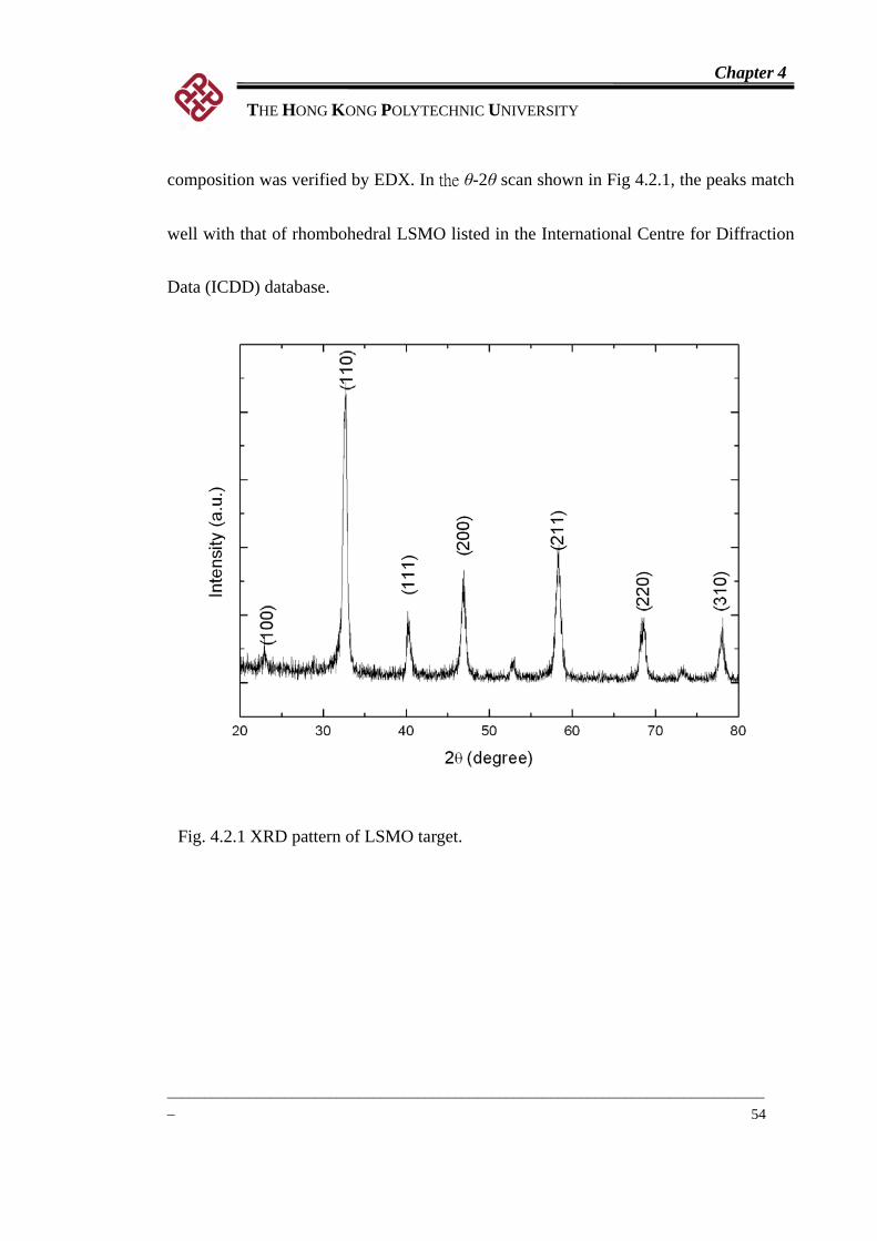
The as-prepared LSMO target was structurally characterized by XRD. Its chemical
Chapter 4
THE HONG KONG POLYTECHNIC UNIVERSITY
__________________________________________________________________________________
54
composition was verified by EDX. In the θ-2θ scan shown in Fig 4.2.1, the peaks match
well with that of rhombohedral LSMO listed in the International Centre for Diffraction
Data (ICDD) database.
Fig. 4.2.1 XRD pattern of LSMO target.
Chapter 4
THE HONG KONG POLYTECHNIC UNIVERSITY
__________________________________________________________________________________
55
4.3 Fabrication of LSMO thin films
The lattice mismatch between film and substrate materials can influence the lattice
parameters of the deposited films, as well as their crystallinity and in-plane epitaxial
relations. In this thesis, the lattice mismatch f is defined as the percentage difference in
the lattice parameters of film and substrate materials:
%100×⎟⎟⎠
⎞⎜⎜⎝
⎛ −=
s
bulks
aaa
f
where abulk and as are lattice constants of the bulk material and the substrate,
respectively.
LSMO has a pseudo-cubic structure with lattice parameter a = 3.87 Å. Lanthanum
aluminum oxide LaAlO3 (LAO), a single-crystal substrate material used in the work,
also possesses a pseudo-cubic structure with lattice parameter 3.79 Å, implying a lattice
mismatch of -2.2 % with LSMO. Strontium titanate SrTiO3 (STO) is another suitable
substrate material because of a small lattice mismatch with LSMO (0.81 %). In this
work, LAO was primarily used as the substrate material, and the epitaxy of films was
generally comparable with LSMO films deposited on STO substrates under identical
conditions in our PLD system.
LSMO thin films were deposited on LAO (100) substrates by PLD method. A laser
Chapter 4
THE HONG KONG POLYTECHNIC UNIVERSITY
__________________________________________________________________________________
56
fluence of 3.6 Jcm-2 and frequency 5 Hz was used for the deposition process. The
chamber base pressure during the deposition and post-deposition annealing processes
was 5 mTorr. During the film deposition process, oxygen was filled into the chamber
and maintained at a pressure of 150 mTorr, when the substrate temperature was
gradually raised to 650 °C. The substrates were then annealed for 10 minutes before
ablation started. The thicknesses of the films were controlled by the deposition time,
according to a calibration rate of ~20 nm/min (the rate was obtained by examining the
cross-section of a thick calibration sample, deposited for a specific duration of time,
under the scanning electron microscope). LSMO thin films of thickness ~50 nm were
deposited. The deposition parameters are summarized in Appendix A (table A).
Chapter 4
THE HONG KONG POLYTECHNIC UNIVERSITY
__________________________________________________________________________________
57
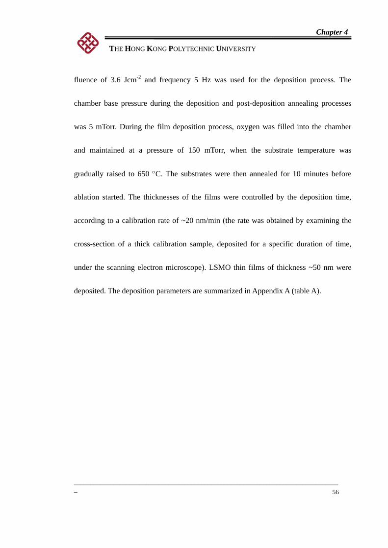
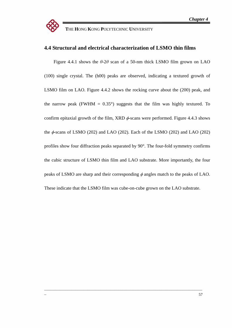
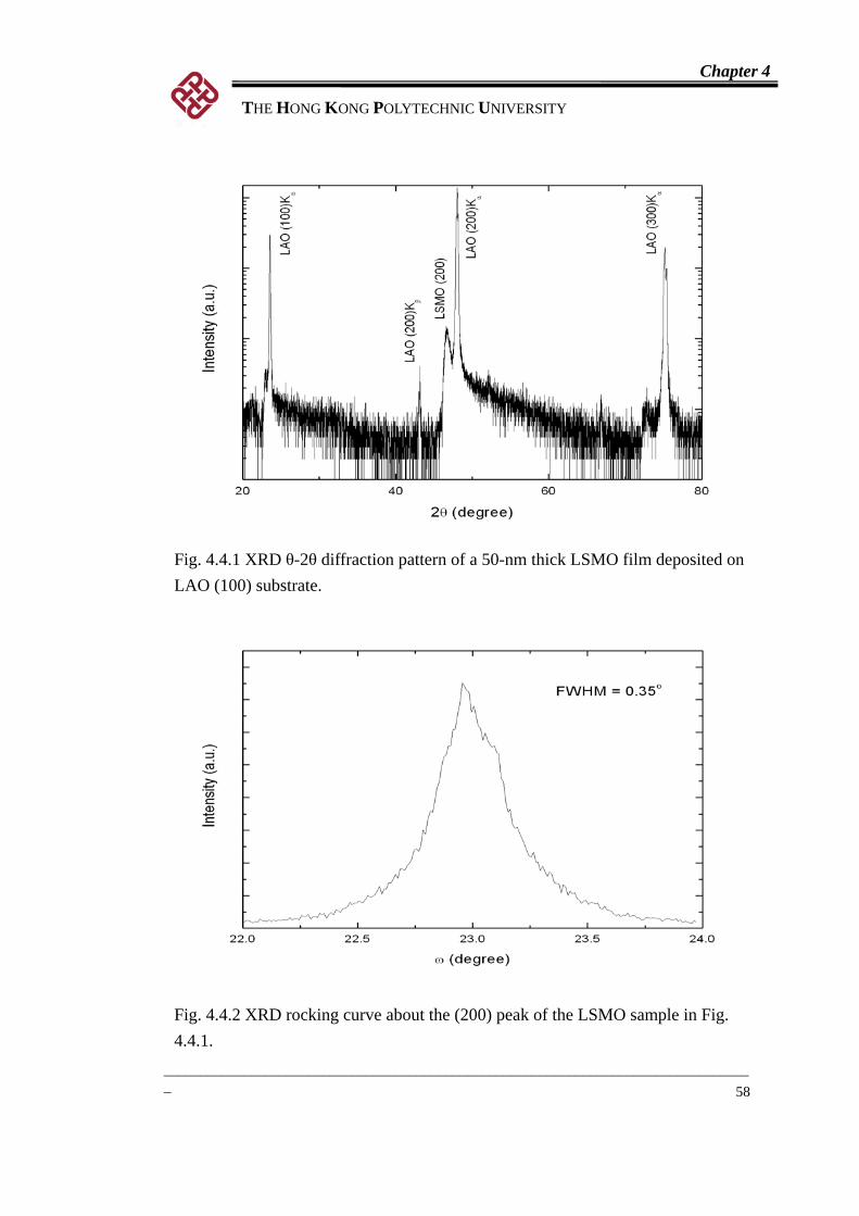
4.4 Structural and electrical characterization of LSMO thin films
Figure 4.4.1 shows the θ-2θ scan of a 50-nm thick LSMO film grown on LAO
(100) single crystal. The (h00) peaks are observed, indicating a textured growth of
LSMO film on LAO. Figure 4.4.2 shows the rocking curve about the (200) peak, and
the narrow peak (FWHM = 0.35°) suggests that the film was highly textured. To
confirm epitaxial growth of the film, XRD φ-scans were performed. Figure 4.4.3 shows
the φ-scans of LSMO (202) and LAO (202). Each of the LSMO (202) and LAO (202)
profiles show four diffraction peaks separated by 90°. The four-fold symmetry confirms
the cubic structure of LSMO thin film and LAO substrate. More importantly, the four
peaks of LSMO are sharp and their corresponding φ angles match to the peaks of LAO.
These indicate that the LSMO film was cube-on-cube grown on the LAO substrate.
Chapter 4
THE HONG KONG POLYTECHNIC UNIVERSITY
Fig. 4.4.1 XRD θ-2θ diffraction pattern of a 50-nm thick LSMO film deposited on LAO (100) substrate.
Fig. 4.4.2 XRD rocking curve about the (200) peak of the LSMO sample in Fig. 4.4.1.
__________________________________________________________________________________
58
Chapter 4
THE HONG KONG POLYTECHNIC UNIVERSITY
_
59
Fig. 4.4.3 φ-scan of the LSMO sample in Fig. 4.4.1. i) LSMO (202) and ii) LAO (202) planes.
_________________________________________________________________________________
Chapter 4
THE HONG KONG POLYTECHNIC UNIVERSITY
__________________________________________________________________________________
60
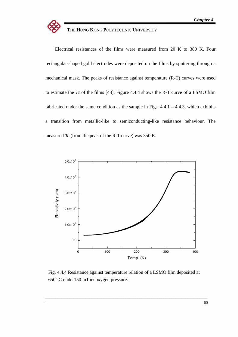
Electrical resistances of the films were measured from 20 K to 380 K. Four
rectangular-shaped gold electrodes were deposited on the films by sputtering through a
mechanical mask. The peaks of resistance against temperature (R-T) curves were used
to estimate the Tc of the films [43]. Figure 4.4.4 shows the R-T curve of a LSMO film
fabricated under the same condition as the sample in Figs. 4.4.1 – 4.4.3, which exhibits
a transition from metallic-like to semiconducting-like resistance behaviour. The
measured Tc (from the peak of the R-T curve) was 350 K.
Fig. 4.4.4 Resistance against temperature relation of a LSMO film deposited at 650 °C under150 mTorr oxygen pressure.
Chapter 4
THE HONG KONG POLYTECHNIC UNIVERSITY
__________________________________________________________________________________
61
4.5 In situ post annealing
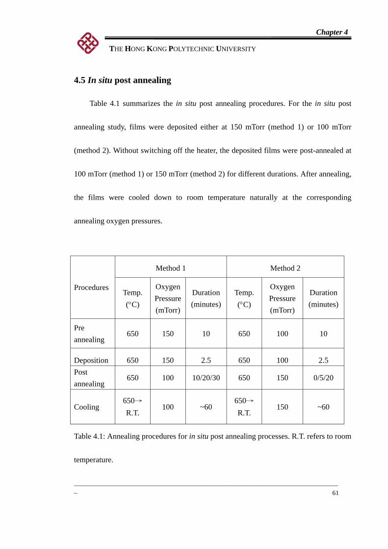
Table 4.1 summarizes the in situ post annealing procedures. For the in situ post
annealing study, films were deposited either at 150 mTorr (method 1) or 100 mTorr
(method 2). Without switching off the heater, the deposited films were post-annealed at
100 mTorr (method 1) or 150 mTorr (method 2) for different durations. After annealing,
the films were cooled down to room temperature naturally at the corresponding
annealing oxygen pressures.
Method 1 Method 2
Procedures Temp. (°C)
Oxygen Pressure (mTorr)
Duration (minutes)
Temp. (°C)
Oxygen Pressure (mTorr)
Duration (minutes)
Pre annealing
650 150 10 650 100 10
Deposition 650 150 2.5 650 100 2.5 Post annealing
650 100 10/20/30 650 150 0/5/20
Cooling 650→
R.T. 100 ~60
650→
R.T. 150 ~60
Table 4.1: Annealing procedures for in situ post annealing processes. R.T. refers to room
temperature.
Chapter 4
THE HONG KONG POLYTECHNIC UNIVERSITY
__________________________________________________________________________________
62
Resistances of the films were measured in the temperature range from 150 K to
380 K. Four rectangular-shaped gold electrodes were deposited on the films by
sputtering through a mechanical mask. Peaks of resistance against temperature curves
were used to estimate the Curie temperatures of the films [43].
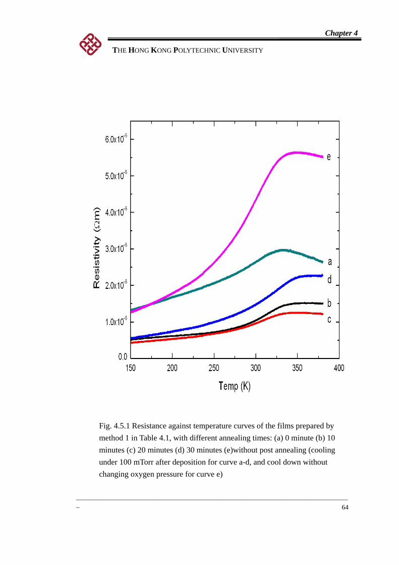
Figure 4.5.1 shows the resistance against temperature plots of LSMO films grown
on LAO at 150 mTorr and then annealed at 100 mTorr for different durations (method 1).
As the post annealing time increased from 0 to 30 minutes, the Curie temperature of
LSMO films increased from 330 K to 365 K. The control sample that was cooled down
immediately after deposition in an oxygen pressure of 150 mTorr is shown in Fig. 4.5.1
(curve e), which had a higher resistance compared with the annealed films (curve a-d).
One of possible reasons for the observation is the diffusion of oxygen out of the films,
when the oxygen pressure was changed to 100 mTorr. As a result, the ratio Mn4+/Mn3+
decreased and ferromagnetic ordering was reduced. However, other possibiliies exist,
such as crystallinity changes [40] and strain relaxation [39] during the annealing
processes, which can affect the TC. Dho et al. [39] reported the results of x-ray
diffraction (XRD) measurements for films that were deposited at 750 °C under different
oxygen pressures (250, 350, and 450 mTorr) and post annealed at 750 °C in an oxygen
Chapter 4
THE HONG KONG POLYTECHNIC UNIVERSITY
__________________________________________________________________________________
63
pressure of 500 mTorr for 30 minutes. As the oxygen pressure increased from 250
mTorr to 450 mTorr, TC changed from 300 K to 360 K. The compressive lattice strain of
the films was relaxed, and the out-of-plane lattice constant was decreased by 0.02 nm.
In order to detect any changes in the lattice structures, I have performed XRD
measurements on all of the film. The changes, if any, were too small to be detected in
this experiment.
Chapter 4
THE HONG KONG POLYTECHNIC UNIVERSITY
_
64
Fig. 4.5.1 Resistance against temperature curves of the films prepared by method 1 in Table 4.1, with different annealing times: (a) 0 minute (b) 10 minutes (c) 20 minutes (d) 30 minutes (e)without post annealing (cooling under 100 mTorr after deposition for curve a-d, and cool down without changing oxygen pressure for curve e)
_________________________________________________________________________________
Chapter 4
THE HONG KONG POLYTECHNIC UNIVERSITY
__________________________________________________________________________________
65
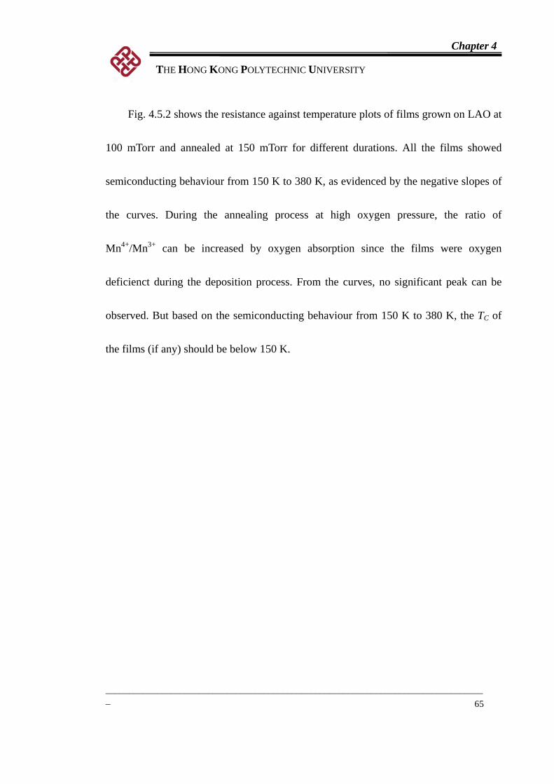
Fig. 4.5.2 shows the resistance against temperature plots of films grown on LAO at
100 mTorr and annealed at 150 mTorr for different durations. All the films showed
semiconducting behaviour from 150 K to 380 K, as evidenced by the negative slopes of
the curves. During the annealing process at high oxygen pressure, the ratio of
Mn4+/Mn3+ can be increased by oxygen absorption since the films were oxygen
deficienct during the deposition process. From the curves, no significant peak can be
observed. But based on the semiconducting behaviour from 150 K to 380 K, the TC of
the films (if any) should be below 150 K.
Chapter 4
THE HONG KONG POLYTECHNIC UNIVERSITY
_
66
Fig. 4.5.2 Resistance against temperature curves of the films prepared by method 2 in Table 4.1, with different annealing times: (a) 0 minute (b) 5 minutes (c) 20 minutes (d) without post annealed (cooling under 150 mTorr after deposition for curve a-c, and cool down without changing oxygen pressure for curve d)
_________________________________________________________________________________
Chapter 4
THE HONG KONG POLYTECHNIC UNIVERSITY
__________________________________________________________________________________
67
4.6 Ex situ post annealing
Table 4.2 summarizes the procedures for ex situ post annealing experiments
performed in this project. For the ex situ post annealing study, films were deposited at
150 mTorr and cooled down to room temperature naturally at the same oxygen pressure.
Then the films were heated up to 650 °C without (method 3) or with (method 4) oxygen
filled into the chamber and annealed for different durations. Finally, the films were
cooled down to room temperature with the oxygen pressure maintained at 150 mTorr.
Resistances of the films were then measured in the temperature range from 150 K to
380 K.
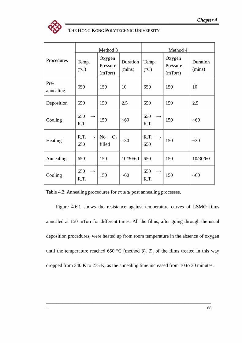
Chapter 4
THE HONG KONG POLYTECHNIC UNIVERSITY
__________________________________________________________________________________
68
Method 3 Method 4
Procedures Temp. (°C)
Oxygen Pressure (mTorr)
Duration (mins)
Temp. (°C)
Oxygen Pressure (mTorr)
Duration (mins)
Pre- annealing
650 150 10 650 150 10
Deposition 650 150 2.5 650 150 2.5
Cooling 650 → R.T.
150 ~60 650 → R.T.
150 ~60
Heating R.T. → 650
No O2 filled
~30 R.T. → 650
150 ~30
Annealing 650 150 10/30/60 650 150 10/30/60
Cooling 650 →
R.T. 150 ~60
650 →
R.T. 150 ~60
Table 4.2: Annealing procedures for ex situ post annealing processes.
Figure 4.6.1 shows the resistance against temperature curves of LSMO films
annealed at 150 mTorr for different times. All the films, after going through the usual
deposition procedures, were heated up from room temperature in the absence of oxygen
until the temperature reached 650 °C (method 3). TC of the films treated in this way
dropped from 340 K to 275 K, as the annealing time increased from 10 to 30 minutes.
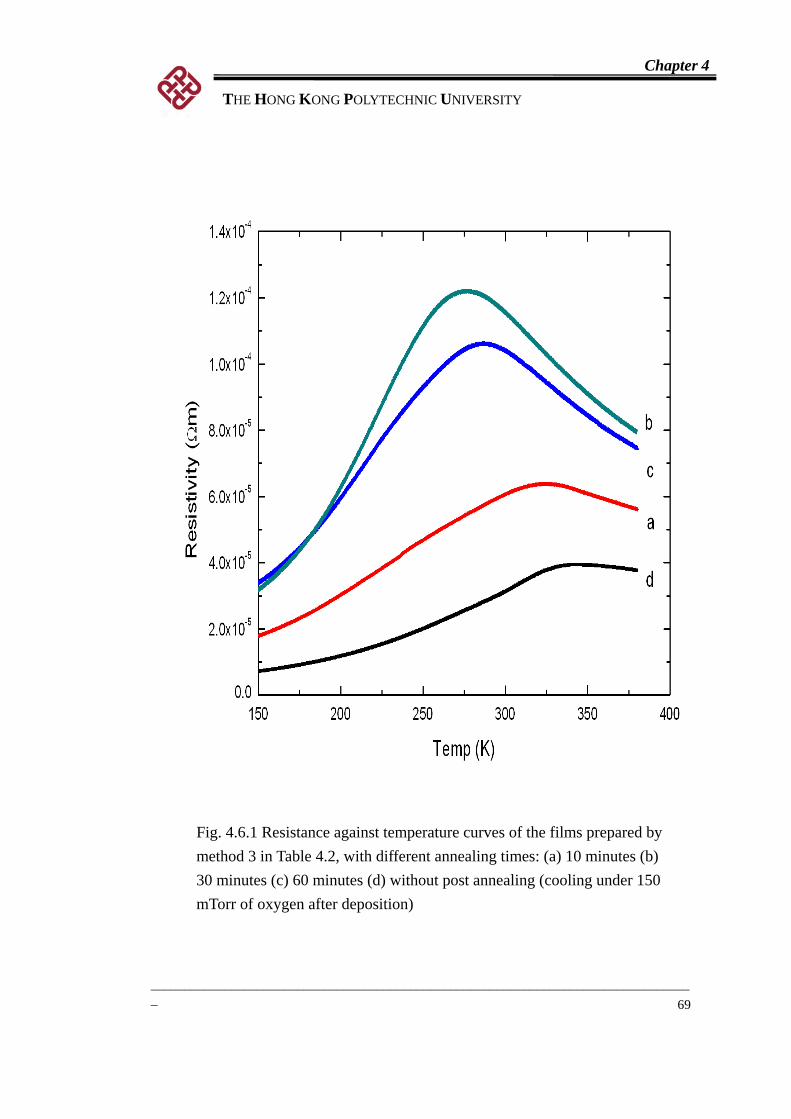
Chapter 4
THE HONG KONG POLYTECHNIC UNIVERSITY
__________________________________________________________________________________
69
Fig. 4.6.1 Resistance against temperature curves of the films prepared by method 3 in Table 4.2, with different annealing times: (a) 10 minutes (b) 30 minutes (c) 60 minutes (d) without post annealing (cooling under 150 mTorr of oxygen after deposition)

Chapter 4
THE HONG KONG POLYTECHNIC UNIVERSITY
__________________________________________________________________________________
70
Fig. 4.6.2 Resistance against temperature curves of the films prepared by method 4 in Table 4.2, with different annealing times: (a) 10 minutes (b) 30 minutes (c) 60 minutes (d) without post annealing (cooling under 150 mTorr of oxygen after deposition).
Chapter 4
THE HONG KONG POLYTECHNIC UNIVERSITY
__________________________________________________________________________________
71
Figure 4.6.2 shows the R-T curves of LSMO films annealed at 150 mTorr. The
chamber was filled with oxygen when heating started at room temperature (method 4),
and we observed that all the curves peaked about 340 K.
By comparing these two figures, we can observe that TC of the films depends
heavily on the correct sequences of post annealing steps. If oxygen was absent from the
chamber during the heating stage before annealing, the films would be oxygen deficient.
This caused the TC of the films to drop significantly, which was shown clearly in Fig.
4.6.1.
Great care therefore has to be taken, during either the deposition or the annealing
processes, to ensure that the film properties are not altered by subsequent processing
steps. For example, if two perovskite layers are deposited and a mechanical mask has to
be inserted before depositing the second layer, method 4 should be used if a high TC of
the film is desired.
4.7 Summary
Single-phased (100) LSMO films were grown on single crystal (100) LAO
substrates epitaxially, and I have investigated the effect of post annealing procedures on
Chapter 4
THE HONG KONG POLYTECHNIC UNIVERSITY
__________________________________________________________________________________
72
the properties of LSMO films. We found that the stability of oxide films were highly
dependent on the oxygen environment during the annealing procedures. This part of
work thus provides useful information for the growth of epitaxial oxide multilayers.
Chapter 5
THE HONG KONG POLYTECHNIC UNIVERSITY
__________________________________________________________________________________
73
CHAPTER 5
Manganite\Metal Spin Valves
5.1 Introduction
LSMO is one of the ferromagnetic oxides being actively researched in the field of
spintronics due to its high spin polarization [38], relatively high Tc (Park et. al., 1998)
and chemical stability. It has been used for GMR junctions [44] and TMR junctions [45].
In both types of junctions, spacers (conductors in GMR junctions, insulators in TMR
junctions) are required to perform certain functions as discussed below.
As mentioned in Chapter 2, the spacer in a spin valve structure is used for
decoupling two ferromagnetic layers, in order to obtain parallel and anti-parallel
magnetization states. On the other hand, for GMR to be observed, spin orientation of the
charge carriers must be conserved as they travel through the spacer layer. The thickness
of the spacer must be comparable with the electronic mean free path for CIP-GMR, or
the spin diffusion lengths for CPP-GMR [17]. Thus, the thickness of the spacer is a
crucial parameter affecting the performance of GMR multilayers.
However, there are a few studies on GMR or TMR junctions which do not have
Chapter 5
THE HONG KONG POLYTECHNIC UNIVERSITY
__________________________________________________________________________________
74
any spacer layers deposited. Ruotolo et al. [46] have experimentally demonstrated that
LSMO\Ni80Fe20 bilayers could exhibit GMR effect. They claimed that the dead layer of
LSMO\Ni80Fe20 interface can be treated as an intrinsic spacer, with its thickness large
enough to suppress magnetic coupling between the bulk of LSMO and NiFe layers.
Singh et al. [47] reported that magnetite (Fe3O4) - manganite (LSMO) bilayers also
exhibited GMR at low temperatures. They claimed that a structurally disordered
interface was formed at the LSMO\Fe3O4 interface due to the 6.7 % lattice mismatch
between the two materials. As the ferromagnetic coupling mechanism in LSMO is
double exchange coupling between Mn3+ and Mn4+ ions [25], the disordered interface
could destroy any double exchange coupling. This will weaken the magnetic coupling
between the two magnetic layers.
The above reports concluded that artificial spacer layers are not strictly necessary
for GMR devices. In this chapter, I report a study on the magneto-transport properties of
LSMO\Co33Fe67 spacerless spin valve structure.
Chapter 5
THE HONG KONG POLYTECHNIC UNIVERSITY
__________________________________________________________________________________
75
5.2 Fabrication of LaNiO3 and LaNiO3\LSMO thin films
In CPP resistance measurements, van de Veerdonk et al. [48] reported that
inhomogeneous current flow in magnetoresistive junctions could induce a large
apparent MR, if the junction resistance was not much larger than the electrode
resistance. It is therefore important to construct CPP GMR junctions with a large
resistance contrast between the junctions and the electrodes.
In this regard, LaNiO3 (LNO) is a good candidate for electrode material. It has a
perovskite pseudo-cubic structure similar to LSMO. Its bulk lattice parameter is a =
3.84 Å. The lattice mismatch between LNO and LAO is -1.3 %. Single-crystal LAO
substrates were therefore used in this work in order to obtain epitaxial growth of LNO
films. In fact, Zhu et al. have shown that LNO films could be epitaxially grown on LAO
(100) substrate with strong (100) orientation [49]. The films had metallic behaviour and
low resistivity (ρ = 3×10⁻⁶ Ωm), which is one order of magnitude less than LSMO, ρ =
5×10⁻⁵ Ωm) [49, 50] and the surfaces can be grown with high smoothness (refer to
Section 5.4 and 5.5). These conditions favoured the use of LNO as bottom electrode.
LNO thin films were deposited on LAO (100) substrates at 650 °C by PLD method.
The deposition parameters are shown in Appendix B. LNO thin films of thickness
Chapter 5
THE HONG KONG POLYTECHNIC UNIVERSITY
__________________________________________________________________________________
76
~100 nm were deposited to test their suitability as bottom electrode layers.
For LNO\LSMO samples, LNO was first deposited on LAO (100) substrates with
the same procedures described above. Afterwards, the films were cooled down to room
temperature naturally at a 150-mTorr oxygen environment. The LNO ablation target
was then replaced by LSMO target, before the samples were heated up again to 650 °C
under an oxygen pressure of 150 mTorr and annealed for 15 minutes. LSMO films were
deposited according to the deposition parameters shown in Appendix A. The deposition
time for the LSMO layer was 5 minutes and the thickness was ~50 nm (refer to Section
4.3). Finally, the bilayers were cooled down to room temperature naturally under an
oxygen pressure of 150 mTorr.
5.3 Structural characterization of LNO and LNO\LSMO thin films
Structural properties of LNO and LNO\LSMO films were studied by XRD.
Figure 5.3.1 shows the θ-2θ scans of a 100-nm thick LNO film grown on LAO (100)
substrate. LNO (200) reflection peak was observed at 46.94°, and the out-of-plane
lattice constant was estimated to be 3.87Å. Since the lattice constant of bulk LNO was
3.84 Å, the LSMO film was under in-plane compressive stress. The FWHM of the LNO
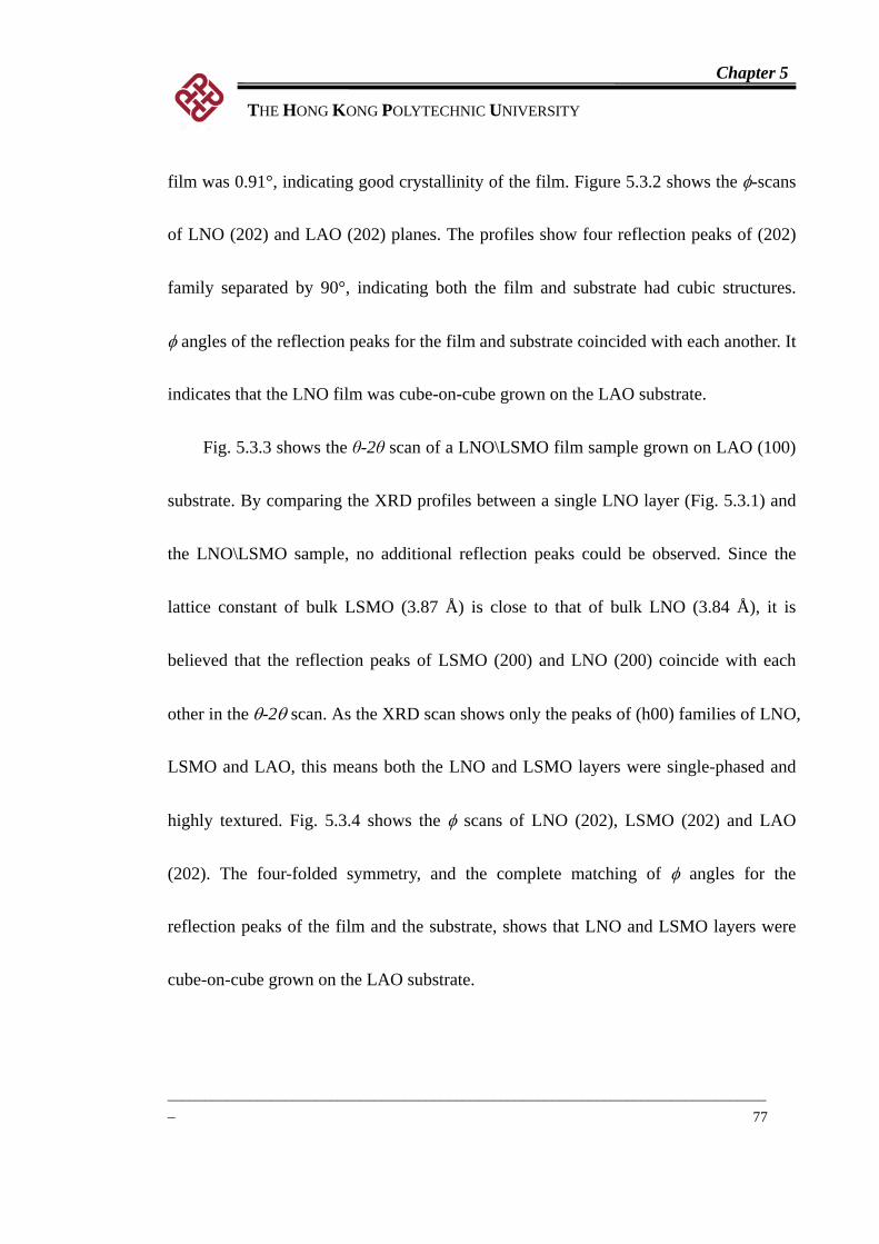
Chapter 5
THE HONG KONG POLYTECHNIC UNIVERSITY
__________________________________________________________________________________
77
film was 0.91°, indicating good crystallinity of the film. Figure 5.3.2 shows the φ-scans
of LNO (202) and LAO (202) planes. The profiles show four reflection peaks of (202)
family separated by 90°, indicating both the film and substrate had cubic structures.
φ angles of the reflection peaks for the film and substrate coincided with each another. It
indicates that the LNO film was cube-on-cube grown on the LAO substrate.
Fig. 5.3.3 shows the θ-2θ scan of a LNO\LSMO film sample grown on LAO (100)
substrate. By comparing the XRD profiles between a single LNO layer (Fig. 5.3.1) and
the LNO\LSMO sample, no additional reflection peaks could be observed. Since the
lattice constant of bulk LSMO (3.87 Å) is close to that of bulk LNO (3.84 Å), it is
believed that the reflection peaks of LSMO (200) and LNO (200) coincide with each
other in the θ-2θ scan. As the XRD scan shows only the peaks of (h00) families of LNO,
LSMO and LAO, this means both the LNO and LSMO layers were single-phased and
highly textured. Fig. 5.3.4 shows the φ scans of LNO (202), LSMO (202) and LAO
(202). The four-folded symmetry, and the complete matching of φ angles for the
reflection peaks of the film and the substrate, shows that LNO and LSMO layers were
cube-on-cube grown on the LAO substrate.
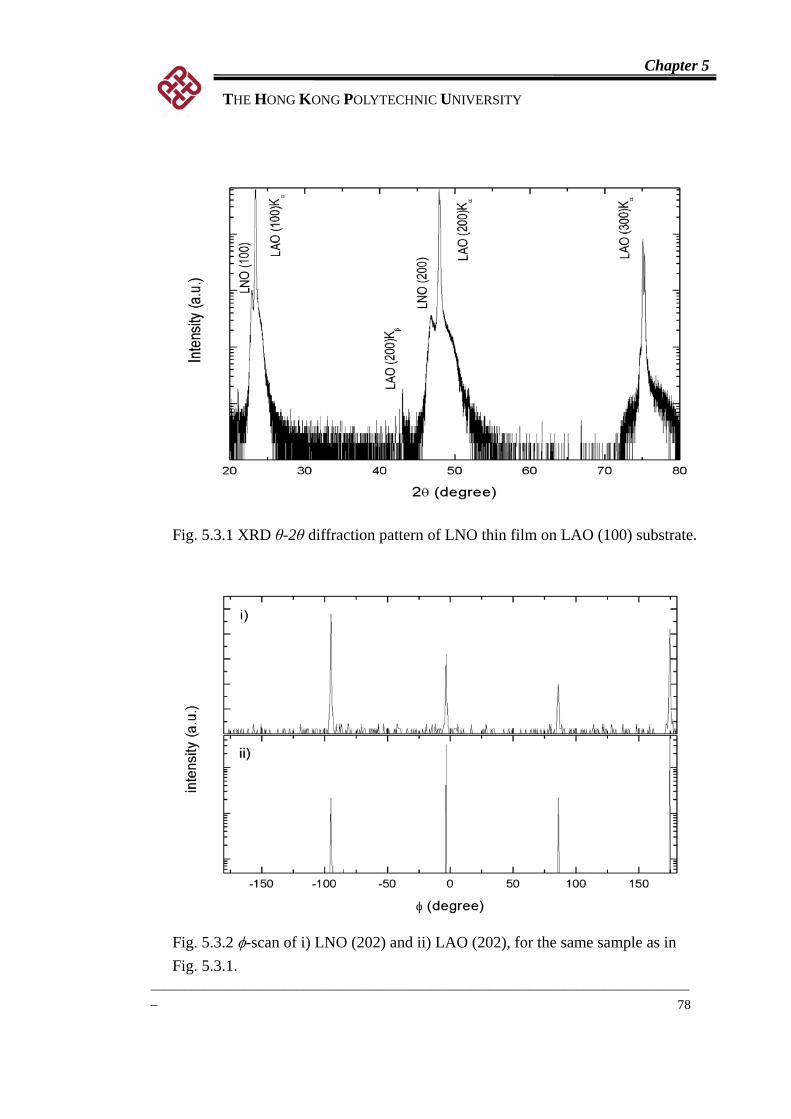
Chapter 5
THE HONG KONG POLYTECHNIC UNIVERSITY
_
Fig. 5.3.1 XRD θ-2θ diffraction pattern of LNO thin film on LAO (100) substrate.
__
Fig. 5.3.2 φ-scan of i) LNO (202) and ii) LAO (202), for the same sample as inFig. 5.3.1.
78
_______________________________________________________________________________
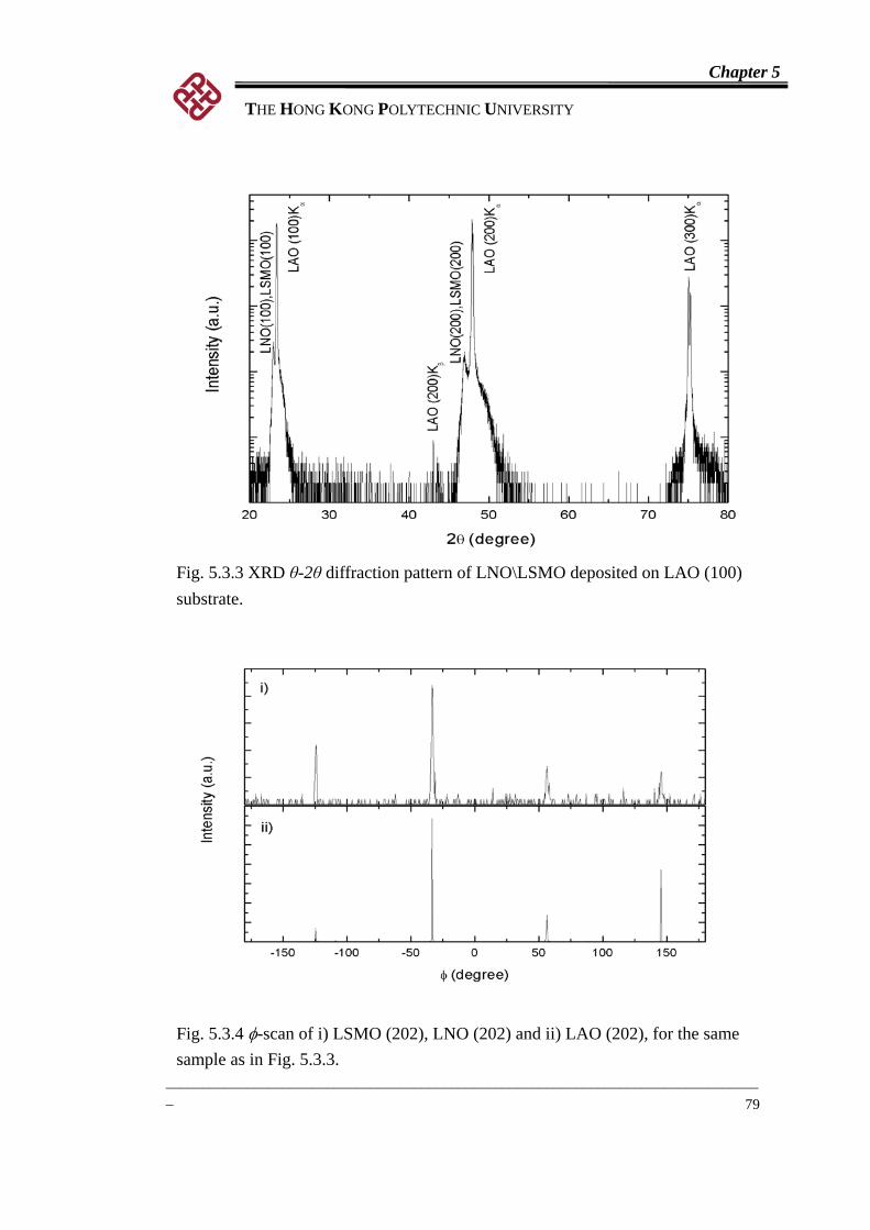
Chapter 5
THE HONG KONG POLYTECHNIC UNIVERSITY
_
79
Fig. 5.3.3 XRD θ-2θ diffraction pattern of LNO\LSMO deposited on LAO (100) substrate.
Fig. 5.3.4 φ-scan of i) LSMO (202), LNO (202) and ii) LAO (202), for the same sample as in Fig. 5.3.3.
_________________________________________________________________________________
Chapter 5
THE HONG KONG POLYTECHNIC UNIVERSITY
__________________________________________________________________________________
80
5.4 Surface morphology of LNO and LNO\LSMO thin films
The surface morphologies of LNO and LNO\LSMO films were investigated by
AFM. Fig. 5.4.1 shows the AFM images of a LNO film (Fig. 5.4.1 (i)) and a
LNO\LSMO sample (Fig. 5.4.1 (ii)). The r.m.s. roughness of LNO and LNO\LSMO
samples were about 0.4 nm and 3.1 nm, respectively. The results indicated that smooth
and continuous LNO thin films can be grown on LAO. However, the roughness
increased as LSMO was deposited on top of LNO. It may be due to the in-plane lattice
mismatch between LNO and LSMO [49].
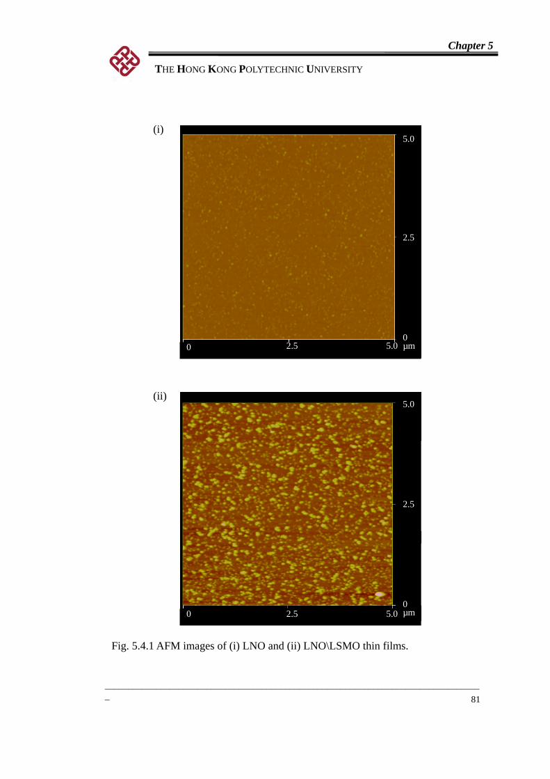
Chapter 5
THE HONG KONG POLYTECHNIC UNIVERSITY
_
81
(i)
_________________________________________________________________________________
Fig. 5.4.1 AFM images of (i) LNO and (ii) LNO\LSMO thin films.
(ii)
µm
5.0
2.5
0 2.5 5.0 0
5.0
2.5
0 2.5 5.0 0 µm
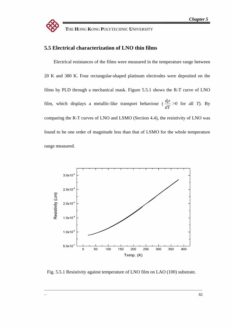
Chapter 5
THE HONG KONG POLYTECHNIC UNIVERSITY
__________________________________________________________________________________
82
5.5 Electrical characterization of LNO thin films
Electrical resistances of the films were measured in the temperature range between
20 K and 380 K. Four rectangular-shaped platinum electrodes were deposited on the
films by PLD through a mechanical mask. Figure 5.5.1 shows the R-T curve of LNO
film, which displays a metallic-like transport behaviour (dTdρ >0 for all T). By
comparing the R-T curves of LNO and LSMO (Section 4.4), the resistivity of LNO was
found to be one order of magnitude less than that of LSMO for the whole temperature
range measured.
Fig. 5.5.1 Resistivity against temperature of LNO film on LAO (100) substrate.
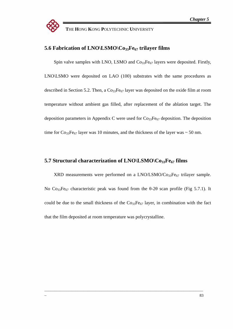
Chapter 5
THE HONG KONG POLYTECHNIC UNIVERSITY
__________________________________________________________________________________
83
5.6 Fabrication of LNO\LSMO\Co33Fe67 trilayer films
Spin valve samples with LNO, LSMO and Co33Fe67 layers were deposited. Firstly,
LNO\LSMO were deposited on LAO (100) substrates with the same procedures as
described in Section 5.2. Then, a Co33Fe67 layer was deposited on the oxide film at room
temperature without ambient gas filled, after replacement of the ablation target. The
deposition parameters in Appendix C were used for Co33Fe67 deposition. The deposition
time for Co33Fe67 layer was 10 minutes, and the thickness of the layer was ~ 50 nm.
5.7 Structural characterization of LNO\LSMO\Co33Fe67 films
XRD measurements were performed on a LNO/LSMO/Co33Fe67 trilayer sample.
No Co33Fe67 characteristic peak was found from the θ-2θ scan profile (Fig 5.7.1). It
could be due to the small thickness of the Co33Fe67 layer, in combination with the fact
that the film deposited at room temperature was polycrystalline.
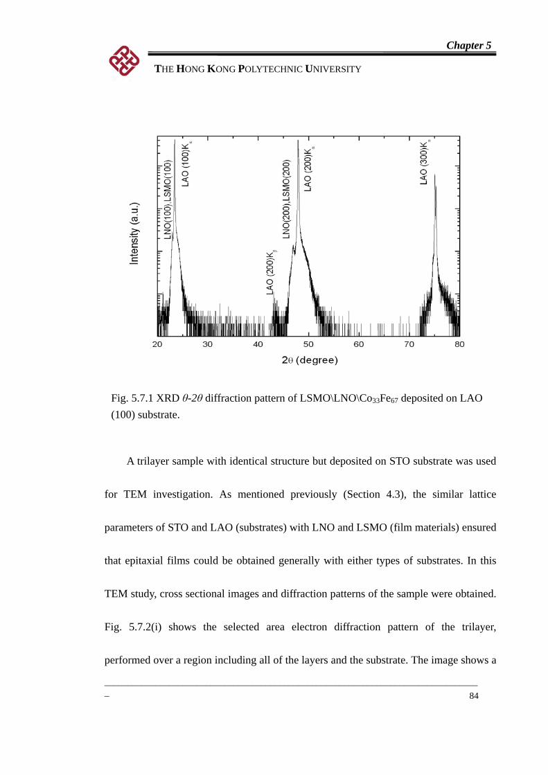
Chapter 5
THE HONG KONG POLYTECHNIC UNIVERSITY
__________________________________________________________________________________
84
Fig. 5.7.1 XRD θ-2θ diffraction pattern of LSMO\LNO\Co33Fe67 deposited on LAO (100) substrate.
A trilayer sample with identical structure but deposited on STO substrate was used
for TEM investigation. As mentioned previously (Section 4.3), the similar lattice
parameters of STO and LAO (substrates) with LNO and LSMO (film materials) ensured
that epitaxial films could be obtained generally with either types of substrates. In this
TEM study, cross sectional images and diffraction patterns of the sample were obtained.
Fig. 5.7.2(i) shows the selected area electron diffraction pattern of the trilayer,
performed over a region including all of the layers and the substrate. The image shows a
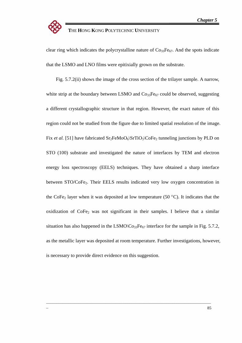
Chapter 5
THE HONG KONG POLYTECHNIC UNIVERSITY
__________________________________________________________________________________
85
clear ring which indicates the polycrystalline nature of Co33Fe67. And the spots indicate
that the LSMO and LNO films were epitixially grown on the substrate.
Fig. 5.7.2(ii) shows the image of the cross section of the trilayer sample. A narrow,
white strip at the boundary between LSMO and Co33Fe67 could be observed, suggesting
a different crystallographic structure in that region. However, the exact nature of this
region could not be studied from the figure due to limited spatial resolution of the image.
Fix et al. [51] have fabricated Sr2FeMoO6\SrTiO3\CoFe2 tunneling junctions by PLD on
STO (100) substrate and investigated the nature of interfaces by TEM and electron
energy loss spectroscopy (EELS) techniques. They have obtained a sharp interface
between STO/CoFe2. Their EELS results indicated very low oxygen concentration in
the CoFe2 layer when it was deposited at low temperature (50 °C). It indicates that the
oxidization of CoFe2 was not significant in their samples. I believe that a similar
situation has also happened in the LSMO\Co33Fe67 interface for the sample in Fig. 5.7.2,
as the metallic layer was deposited at room temperature. Further investigations, however,
is necessary to provide direct evidence on this suggestion.
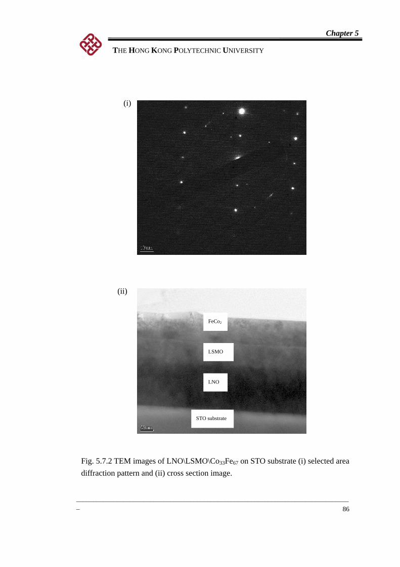
Chapter 5
THE HONG KONG POLYTECHNIC UNIVERSITY
_
86
(i)
(ii)
FeCo2
LSMO
LNO
STO substrate
Fig. 5.7.2 TEM images of LNO\LSMO\Co33Fe67 on STO substrate (i) selected area diffraction pattern and (ii) cross section image.
_________________________________________________________________________________

Chapter 5
THE HONG KONG POLYTECHNIC UNIVERSITY
__________________________________________________________________________________
87
5.8 Magnetic characterization of LNO\LSMO\Co33Fe67
VSM was used to study the magnetic properties of the samples. Hysteresis (M(H))
loops were measured at 100 K with the magnetic field applied parallel to the film plane
along the substrate’s [001] axis. Fig. 5.8.1 shows M(H) loops of Co33Fe67 (i) and
LNO\LSMO (ii). The coercivity values of Co33Fe67 and LSMO were 20 Oe and 105 Oe
respectively. The difference of coercivity values was large enough to obtain
well-defined parallel and anti-parallel configurations in the pseudo spin valve samples.
Fig. 5.8.2(i) shows the M(H) loop of LNO\LSMO\Co33Fe67 at 100 K. It clearly
shows two distinct coercive fields at 20 Oe and 100 Oe, corresponding to the Co33Fe67
and LSMO layers, respectively. In Section 5.7, we mentioned that an interface region
was observed between LSMO and Co33Fe67. This suggests that the interface region
acted as a spacer, which decoupled the LSMO and Co33Fe67 layers effectively.
Fig. 5.8.2(ii) shows the M(H) loop measured at 10 K and 50 K. By comparing with
Fig. 5.8.2(i), it reveals that the coercivity of both LSMO and Co33Fe67 were increased.
Also, well-established parallel and anti-parallel configurations of M(H) loop were still
obtained.
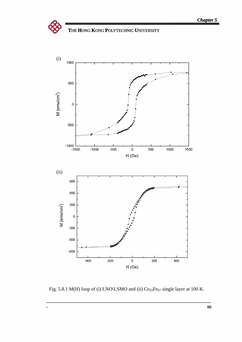
Chapter 5
THE HONG KONG POLYTECHNIC UNIVERSITY
_
88
Chapter 5
THE HONG KONG POLYTECHNIC UNIVERSITY
_
88
(i)
(ii)
Fig. 5.8.1 M(H) loop of (i) LNO\LSMO and (ii) Co33Fe67 single layer at 100 K.
__________________________________________________________________________________________________________________________________________________________________
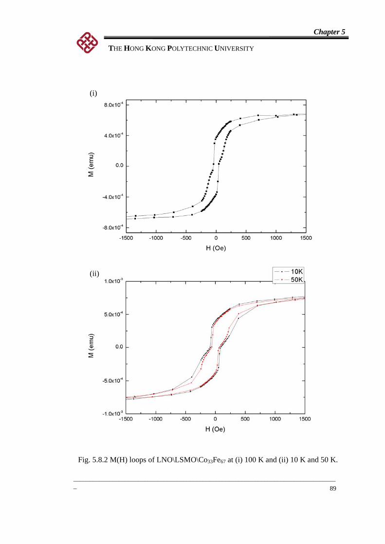
Chapter 5
THE HONG KONG POLYTECHNIC UNIVERSITY
_
89
(i)
(ii)
Fig. 5.8.2 M(H) loops of LNO\LSMO\Co33Fe67 at (i) 100 K and (ii) 10 K and 50 K.
_________________________________________________________________________________
Chapter 5
THE HONG KONG POLYTECHNIC UNIVERSITY
__________________________________________________________________________________
90
5.9 Magneto-transport characterization of LNO\LSMO
In Chapter 2, I introduced different types of MR. In this work, I aimed at
investigating the GMR effect of CPP pseudo spin valve structure. However, other types
of MR, such as AMR from the Co33Fe67 and LSMO layers, can contribute to the
observed MR. While the AMR effect is small for Co33Fe67 (less than 0.2 %) [5], it can
be substantial in polycrystalline LSMO films (up to 15 % at a field of 1500 Oe) [52].
Such a MR ratio can be comparable with that of the GMR effect. Therefore, the AMR
effect of LSMO films has to be checked.
To study the magneto-transport properties of LSMO, LNO\LSMO\Pt junctions
were fabricated (Fig. 5.9.1(i)). LNO films were deposited on LAO substrates as bottom
electrodes. Then LSMO layers were deposited through a thin stainless steel shadow
mask with 200 µm squares. Finally, Pt electrodes were deposited on top of LSMO, by
using the same shadow mask.
Chapter 5
THE HONG KONG POLYTECHNIC UNIVERSITY
__________________________________________________________________________________
91
Pt
LSMO
LNO
LAO substrate
(i)
Fig. 5.9.2 shows the MR measured with magnetic field applied parallel or
perpendicular to the junctions (Fig. 5.9.1(ii) and (iii)) at 20 K. Here, the MR is defined
as
)()()(
HcRHcRHR − (5.9.1)
where Hc is the coercivity. The maximum magnitude of MR obtained was smaller than
0.1 % (within the field range of ±1 kOe) in both configurations. However, the graph of
Fig. 5.9.1(i) Schematic diagram of a LNO\LSMO\Pt junction. Configurations for magneto-transport measurements: (ii) current perpendicular to magnetic field across the junction, (iii) current parallel to magnetic field across the junction.
LAO substrate
LNO
LSMO
Pt
I+ V+
V-I-
Magnetic field
LAO substrate
LNO
LSMO
Pt
I+ V+
I- V-
Magnetic field
(ii) (iii)
Chapter 5
THE HONG KONG POLYTECHNIC UNIVERSITY
__________________________________________________________________________________
92
MR against magnetic field (MR(H)) indicates that both measurements have shown
negative MR behaviour. As mentioned in Chapter 2, the sign of MR depends on the
applied current and magnetic field directions for AMR effect. That means the AMR
effect was not significant. One of possible reasons for the observation was due to the
spin-dependent scattering of polarized electrons at the grain boundaries, which is a
manifestation of the GMR effect [52].
Chapter 5
THE HONG KONG POLYTECHNIC UNIVERSITY
__________________________________________________________________________________
93
(i)
(ii)
Fig. 5.9.2 MR(H) of LSMO with (i) H applied parallel to the current, and (ii) H applied perpendicular to the current at 20K.
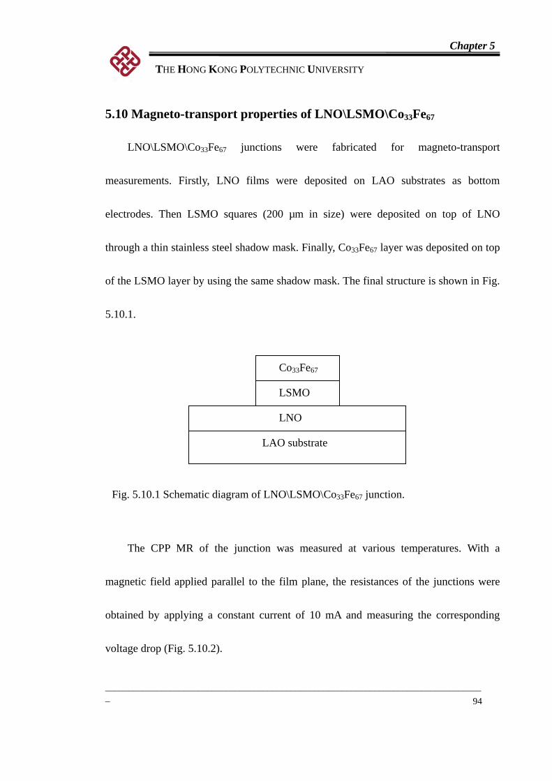
Chapter 5
THE HONG KONG POLYTECHNIC UNIVERSITY
__________________________________________________________________________________
94
5.10 Magneto-transport properties of LNO\LSMO\Co33Fe67
LNO\LSMO\Co33Fe67 junctions were fabricated for magneto-transport
measurements. Firstly, LNO films were deposited on LAO substrates as bottom
electrodes. Then LSMO squares (200 µm in size) were deposited on top of LNO
through a thin stainless steel shadow mask. Finally, Co33Fe67 layer was deposited on top
of the LSMO layer by using the same shadow mask. The final structure is shown in Fig.
5.10.1.
Co33Fe67
LSMO
LNO
LAO substrate
Fig. 5.10.1 Schematic diagram of LNO\LSMO\Co33Fe67 junction.
The CPP MR of the junction was measured at various temperatures. With a
magnetic field applied parallel to the film plane, the resistances of the junctions were
obtained by applying a constant current of 10 mA and measuring the corresponding
voltage drop (Fig. 5.10.2).
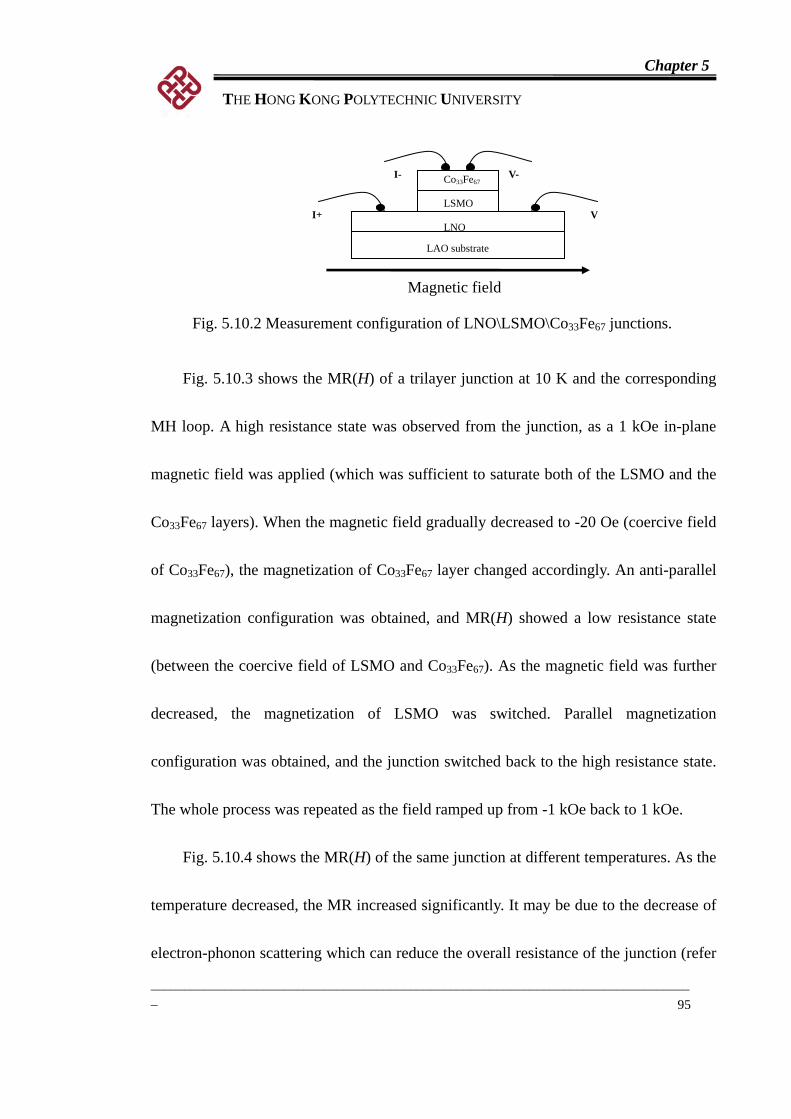
Chapter 5
THE HONG KONG POLYTECHNIC UNIVERSITY
__________________________________________________________________________________
95
LAO substrate
LNO
LSMO
Co33 67Fe
I+ V
V- I-
Magnetic field
Fig. 5.10.2 Measurement configuration of LNO\LSMO\Co33Fe67 junctions.
Fig. 5.10.3 shows the MR(H) of a trilayer junction at 10 K and the corresponding
MH loop. A high resistance state was observed from the junction, as a 1 kOe in-plane
magnetic field was applied (which was sufficient to saturate both of the LSMO and the
Co33Fe67 layers). When the magnetic field gradually decreased to -20 Oe (coercive field
of Co33Fe67), the magnetization of Co33Fe67 layer changed accordingly. An anti-parallel
magnetization configuration was obtained, and MR(H) showed a low resistance state
(between the coercive field of LSMO and Co33Fe67). As the magnetic field was further
decreased, the magnetization of LSMO was switched. Parallel magnetization
configuration was obtained, and the junction switched back to the high resistance state.
The whole process was repeated as the field ramped up from -1 kOe back to 1 kOe.
Fig. 5.10.4 shows the MR(H) of the same junction at different temperatures. As the
temperature decreased, the MR increased significantly. It may be due to the decrease of
electron-phonon scattering which can reduce the overall resistance of the junction (refer

Chapter 5
THE HONG KONG POLYTECHNIC UNIVERSITY
__________________________________________________________________________________
96
to Fig.5.10.5). Magnon scattering, which can be greatly suppressed at low temperatures
(< Tc), can reduce the GMR effect as mentioned in Section 2.2.3. An increase of spin
polarization with a decreasing temperature is also a possible reason of the MR
enhancement. At 10 K, a MR ratio of 1.65 % was obtained at 500 Oe, which was much
greater than that of a single layer of LSMO shown in previous section
From Fig 5.10.3, an inverse GMR behaviour was observed. Vouille et al. [17]
reported that inverse GMR effect can obtained by using two materials with different
signs of spin asymmetries. On the other hand, the sign of MR also depends on the
interfacial spin asymmetry [17, 53]. Spin polarization is defined by
↓↑
↓↑ −=nn
P + nn
(5.9.1)
where ni (i = ↑and ↓) is the density of state of the spin sub-band i at Fermi level. As
nce measurements, van de Veerdonk et al. [48] reported that an
inho
LSMO is a positive spin polarization material, I suggest that the inverse GMR of our
junction may be due to the negative spin polarization of either bulk Co33Fe67 or LSMO\
Co33Fe67 interface
In CPP resista
mogeneous current flow could induce a large apparent MR, if the junction
resistance was not much larger than the electrode resistance. Calculations by Ruotolo et
Chapter 5
THE HONG KONG POLYTECHNIC UNIVERSITY
__________________________________________________________________________________
97
al. [46] showed that LSMO (ρ = 1.2×10⁻⁶ Ωm at 4.2 K) junctions of area 100 µm×70 µm,
when used as the bottom electrode, could rule out any geometrical MR effect. For my
200-µm square junctions, I used LNO as the bottom electrode of the junction, with
resistivity smaller than LSMO. In my junction showed in Fig. 5.10.1, the junction
resistance (Rj) includes the resistance of LSMO and LSMO\Co33Fe67 interface. As the
resistance of LSMO was RLSMO = 66 Ω/sq and LNO electrode was RLNO = 8.9 Ω/sq,
corresponding to resistivity ρLSMO =3.3×10⁻⁶ Ωm and ρLNO =8.9×10⁻⁷ Ωm measured at
20 K. The ratio RLSMO/RLNO was 7.4. Thus, the ratio of Rj/Rlead was much larger than
that value. According to van de Veerdonk et al. [48], the ratio was large enough that the
geometrical effect could be neglected.
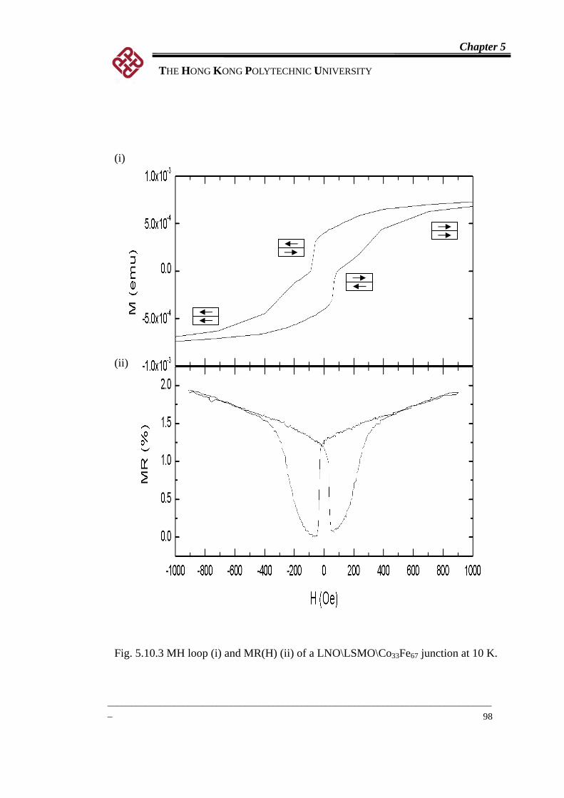
Chapter 5
THE HONG KONG POLYTECHNIC UNIVERSITY
_
98
(i)
(ii)
Fig. 5.10.3 MH loop (i) and MR(H) (ii) of a LNO\LSMO\Co33Fe67 junction at 10 K.
_________________________________________________________________________________
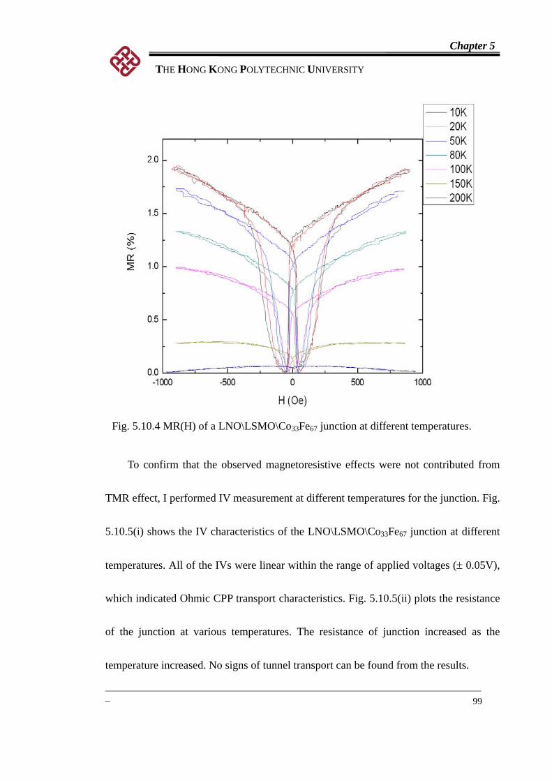
Chapter 5
THE HONG KONG POLYTECHNIC UNIVERSITY
__________________________________________________________________________________
99
Fig. 5.10.4 MR(H) of a LNO\LSMO\Co33Fe67 junction at different temperatures.
To confirm that the observed magnetoresistive effects were not contributed from
TMR effect, I performed IV measurement at different temperatures for the junction. Fig.
5.10.5(i) shows the IV characteristics of the LNO\LSMO\Co33Fe67 junction at different
temperatures. All of the IVs were linear within the range of applied voltages (± 0.05V),
which indicated Ohmic CPP transport characteristics. Fig. 5.10.5(ii) plots the resistance
of the junction at various temperatures. The resistance of junction increased as the
temperature increased. No signs of tunnel transport can be found from the results.
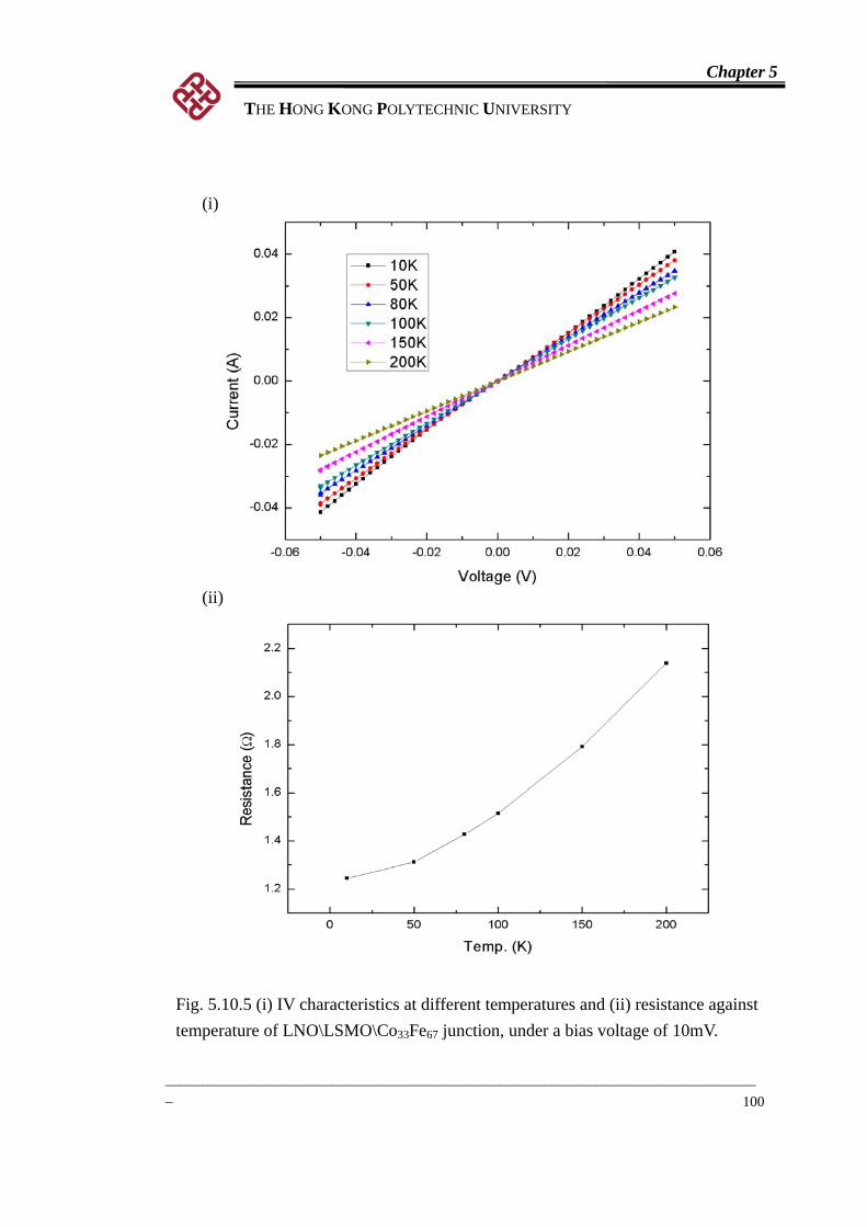
Chapter 5
THE HONG KONG POLYTECHNIC UNIVERSITY
__________________________________________________________________________________
100
Fig. 5.10.5 (i) IV characteristics at different temperatures and (ii) resistance against temperature of LNO\LSMO\Co33Fe67 junction, under a bias voltage of 10mV.
(i)
(ii)
Chapter 5
THE HONG KONG POLYTECHNIC UNIVERSITY
__________________________________________________________________________________
101
5.11 Summary
It has been shown that single-phased (100) LNO films could be epitaxially grown
on (100) LAO single crystal substrates. Also single-phased (100) LSMO films can be
cube-on-cube grown on (100) LNO with good crystallinity. I have fabricated
LNO\LSMO\Co33Fe67 junctions and investigated their magneto-transport behaviour. I
demonstrated the possibility of fabricating pseudo spin valves without using an extrinsic
spacer. The interface between LSMO and Co33Fe67 can be treated as an intrinsic spacer
in pseudo spin valve fabrication.
Chapter 6
THE HONG KONG POLYTECHNIC UNIVERSITY
__________________________________________________________________________________
102
CHAPTER 6
Conclusions
Post annealing of LSMO films
LSMO films have been fabricated on LAO single crystal substrates by PLD. From
the XRD measurements, it has been shown that single-phased (100) LSMO films could
be epitaxially grown on LAO(100) single crystal substrates with high crystallinity and
strong orientations. The peaks of resistance against temperature (R-T) profiles were
used to estimate the Curie temperatures of the films. R-T curves of as-grown LSMO
films had a transition from metallic-like to semiconducting-like resistance behaviour,
similar to results reported in literature.
The estimated Curie temperatures of LSMO films were shown to vary according to
deposition conditions, as well as annealing processes. I have investigated the effect of
different post annealing on the properties of LSMO films. The results indicated that the
stability of oxide films was highly dependent on the oxygen environment, annealing
steps and procedures.

Chapter 6
THE HONG KONG POLYTECHNIC UNIVERSITY
__________________________________________________________________________________
103
LNO\LSMO bilayers
I have fabricated LNO films on LAO single crystal substrates, serving as bottom
electrodes for GMR junctions. The XRD results showed that (100) LNO could be
epitaxially grown on (100) LAO single crystal substrates. Single-phased (100) LSMO
films can be cube-on-cube grown on top of (100) LNO films with good crystallinity.
The surface morphology of LNO and LNO\LSMO films were investigated by AFM.
The r.m.s. roughness of LNO and LNO\LSMO samples were about 0.4 nm and 3.1 nm,
respectively. The results indicated that smooth and continuous LNO thin films can be
grown on LAO, and roughness increased as LSMO was deposited on top of LNO.
Electrical resistances of the LNO films were measured in the temperature range
between 20 K and 380 K. The R-T curve of LNO film, which displayed metallic-like
behaviour, showed resistivity values that was at least one order of magnitude less than
that of LSMO films for the whole temperature range measured. Besides,
magneto-transport properties of LNO\LSMO bilayers were investigated. MR
measurements indicated that AMR was not significant, although GMR effect was
present due to spin-dependent scattering of polarized electron at grain boundaries.
Chapter 6
THE HONG KONG POLYTECHNIC UNIVERSITY
__________________________________________________________________________________
104
LNO\LSMO\Co33Fe67 trilayers
I have also fabricated LNO\LSMO\Co33Fe67 trilayers and investigated their
structural and magnetic properties, and magneto-transport behaviour. XRD could not
show characteristic peaks related to Co33Fe67. It could be due to the small thickness of
Co33Fe67, in combination with the fact that films deposited at room temperature were
polycrystalline. The latter suggestion was further supported by TEM study of a trilayer
sample with identical structure but deposited on STO(100) substrate. Selected area
electron diffraction pattern of the trilayer showed a clear ring, which indicated the
polycrystalline nature of Co33Fe67. An interface region between LSMO and Co33Fe67
was observed in the cross sectional TEM image of the trilayer sample.
VSM was used to study the magnetic properties of trilayer samples. The coercivity
values of Co33Fe67 and LSMO were 20 Oe and 105 Oe respectively. M(H) loop of
LNO\LSMO\Co33Fe67 at 100 K clearly showed two distinct coercive fields at 20 Oe and
100 Oe, corresponding to the Co33Fe67 and LSMO layers, respectively. This suggested
that the interface region acted as a spacer, which reduced the coupling between LSMO
and Co33Fe67 layers.
In magneto transport measurements, the excellent matching of MR(H) and MH
Chapter 6
THE HONG KONG POLYTECHNIC UNIVERSITY
__________________________________________________________________________________
105
loops helped to distinguish the parallel and anti parallel resistance states in the trilayer
sample, demonstrating the GMR behaviour. The inverse GMR of the junctions may be
due to either bulk Co33Fe67 or interface between two ferromagnetic layers with negative
spin polarization.
In conclusion, I have successfully demonstrated the fabrication of pseudo spin
valves without using extrinsic spacers. The interfaces between magnetic oxides and
metals can be treated as intrinsic spacers in pseudo spin valve fabrications. However,
the MR shown by the trilayer samples was small and observable only at low
temperatures. It may be due to the nature or the thickness of the interface layer. In order
to obtain higher MR ratios, more thorough understandings of the interface physics and
film growth processes are needed.
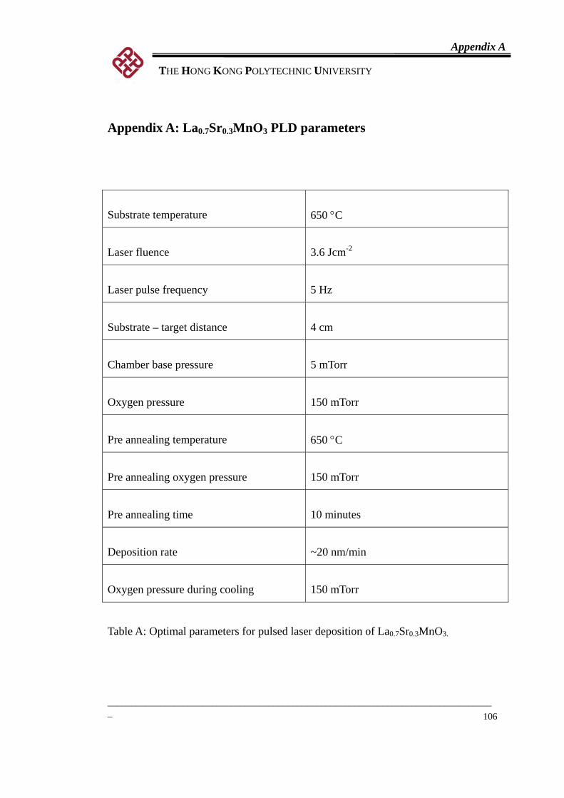
Appendix A
THE HONG KONG POLYTECHNIC UNIVERSITY
__________________________________________________________________________________
106
Appendix A: La0.7Sr0.3MnO3 PLD parameters
Substrate temperature 650 °C
Laser fluence 3.6 Jcm-2
Laser pulse frequency 5 Hz
Substrate – target distance 4 cm
Chamber base pressure 5 mTorr
Oxygen pressure 150 mTorr
Pre annealing temperature 650 °C
Pre annealing oxygen pressure 150 mTorr
Pre annealing time 10 minutes
Deposition rate ~20 nm/min
Oxygen pressure during cooling 150 mTorr
Table A: Optimal parameters for pulsed laser deposition of La0.7Sr0.3MnO3.
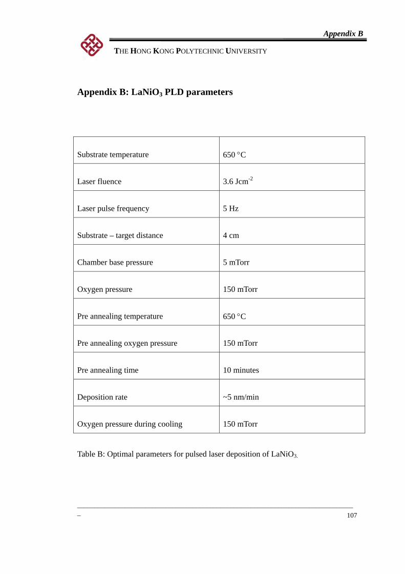
Appendix B
THE HONG KONG POLYTECHNIC UNIVERSITY
__________________________________________________________________________________
107
Appendix B: LaNiO3 PLD parameters
Substrate temperature 650 °C
Laser fluence 3.6 Jcm-2
Laser pulse frequency 5 Hz
Substrate – target distance 4 cm
Chamber base pressure 5 mTorr
Oxygen pressure 150 mTorr
Pre annealing temperature 650 °C
Pre annealing oxygen pressure 150 mTorr
Pre annealing time 10 minutes
Deposition rate ~5 nm/min
Oxygen pressure during cooling 150 mTorr
Table B: Optimal parameters for pulsed laser deposition of LaNiO3.
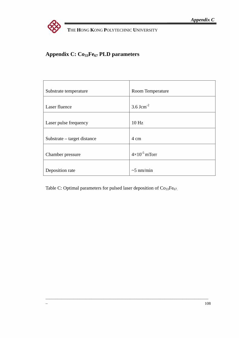
Appendix C
THE HONG KONG POLYTECHNIC UNIVERSITY
__________________________________________________________________________________
108
Appendix C: Co33Fe67 PLD parameters
Substrate temperature Room Temperature
Laser fluence 3.6 Jcm-2
Laser pulse frequency 10 Hz
Substrate – target distance 4 cm
Chamber pressure 4×10⁻⁵ mTorr
Deposition rate ~5 nm/min
Table C: Optimal parameters for pulsed laser deposition of Co33Fe67.
References
THE HONG KONG POLYTECHNIC UNIVERSITY
__________________________________________________________________________________
109
References
[1] R. J. Soulen, Jr., J. M. Byers, M. S. Osofsky, B. Nadgorny, T. Ambrose, S. F.
Cheng, P. R. Broussard, C. T. Tanaka, J. Nowak, J. S. Moodera, A. Barry, and J.
M. D. Coey, “Measuring the spin polarization of a metal with a superconducting
point contact”, Science 282, 85 (1998).
[2] J. M. Daughton, “GMR applications”, J. Magn. Magn. Mater. 192, 334-342 (1999).
[3] T. R. McGuire and R. I. Potter, “Anisotropic magnetoresistance in ferromagnetic
3d alloys”, IEEE Trans. Magn. 11, 1018-1038 (1975).
[4] M. Julliere, “Tunneling between ferromagnetic films”, Phys. Lett. A 54, 225-226
(1975).
[5] J. S. Moodera, L. R. Kinder, T. M. Wong, and R. Meservey, “Large
magnetoresistance at room temperature in ferromagnetic thin film tunnel
junctions”, Phys. Rev. Lett. 74, 3273-3276 (1995).
[6] Djayaprawira, D. David, K. Tsunekawa, M. Nagai, H. Maehara, S. Yamagata, N.
Watanabe, S. Yuasa, Y. Suzuki and K. Ando, “230% room-temperature
References
THE HONG KONG POLYTECHNIC UNIVERSITY
__________________________________________________________________________________
110
magnetoresistance in CoFeB/MgO/CoFeB magnetic tunnel junctions”, Appl. Phys.
Lett. 86, 092502 (2005).
[7] S. Jin, T. H. Tiefel, M. McCormack, R. A. Fastnacht, R. Ramesh, and L. H. Chen,
“Thousandfold change in resistivity in magnetoresistive La-Ca-Mn-O Films”,
Science 264, 413-415 (1994).
[8] K. I. Kobayashi, T. Kimura, H. Sawada, K. Terakura, and Y. Tokura, “Double
perovskites”, Nature 395, 677 (1998).
[9] M. N. Baibich, J. M. Broto, A. Fert, F. N. Van Dau, F. Petroff and P. Eitenne,
“Giant magnetoresistance of (001)Fe / (001)Cr magnetic superlattices”, Phys. Rev.
Lett. 61, 2472-2475 (1988).
[10] J. Mathon, “Exchange interactions and giant magnetoresistance in magnetic
multilayers”, Contemporary Physics 32, 143-156 (1991).
[11] M.M.H. Willekens, T.G.S.M. Rijks, H.J.M. Swagten and W.J.M. deJonge,
“Interface intermixing and magnetoresistance in Co/Cu spin valves with uncoupled
Co layers”, J. Appl. Phys. 78, 7202-7209 (1995).
References
THE HONG KONG POLYTECHNIC UNIVERSITY
__________________________________________________________________________________
111
[12] A. Ruotolo, “Focused ion beam patterning and imaging of novel spintronic devices
for digital magnetic data storage, magnetic field sensing and quantum computing”,
PhD Thesis, University of Naples, (2006).
[13] J. Mathon, “Ab initio calculation of the perpendicular giant magnetoresistance of
finite Co/Cu(001) and Fe/Cr(001) superlattices with fluctuating layer thicknesses”,
Phys. Rev. B 55, 960-969 (1997).
[14] S.S.P. Parkin, “Systematic variation of the strength and oscillation period of
indirect magnetic exchange coupling through the 3d, 4d, and 5d transition metals”,
Phys. Rev. Lett. 67, 3598 (1991)
[15] N. F. Mott, “Electrons in transition metals”, Advances in Physics 13, 325 (1964).
[16] J. F. Gregg, I. Petej, E. Jouguelet and C. Dennis, “Spin electronics” , J. Phys. D:
Appl. Phys. 35, R121-R155 (2002).
[17] A. Vouille, A. Barthelemy, F. Elokan Mpondo, A. Fert, P. A. Schroeder, S. Y. Hsu,
A. Reilly and R. Loloee, “Microscopic mechanisms of giant magnetoresistance”,
Phys. Rev. B 60, 6710-6722 (1999).
References
THE HONG KONG POLYTECHNIC UNIVERSITY
__________________________________________________________________________________
112
[18] B. Dieny, V. S. Speriosu, S. S. P. Parkin, B. A. Gurney, D. R. Wilhoit and D. Mauri,
“Giant magnetoresistive in soft ferromagnetic multilayers”, Phys. Rev. B 43,
1297-1300 (1991).
[19] J. Nogués, and I. K. Schuller, “Exchange bias”, J. Magn. Magn. Mater. 192,
203-232 (1999).
[20] W. S. Lew, A. Samad, S. P. Li, L. Lopez-Diaz, G. X. Cheng and J. A. C. Bland,
“Magnetic properties of epitaxial NiFe/Cu/Co spin-valve structures on GaAs(001)”,
J. Appl. Phys. 87, 5947-5949 (2000).
[21] W. Zou, H. N. G. Wadley, X. W. Zhou and R. A. Johnson, “Surfactant-mediated
growth of giant magnetoresistance multilayers”, Phys. Rev. B 64, 174418 (2001).
[22] G. H. Jonker and J. H. Van Santen, “Ferromagnetic compounds of manganese with
perovskite structure”, Physica 16, 337-349 (1950).
[23] J. H. Van Santen and G. H. Jonker, “Electrical conductivity of ferromagnetic
compounds of manganese with perovskite structure”, Physica 16, 599-600 (1950).
[24] R. Von Helmolt, J. Wecker, B. Holzapfel, L. Schultz and K. Samwer, “Giant
References
THE HONG KONG POLYTECHNIC UNIVERSITY
__________________________________________________________________________________
113
negative magnetoresistance in perovskitelike La2/3Ba1/3MnOx ferromagnetic films”,
Phys. Rev. Lett. 71, 2331-2333 (1993).
[25] Haghiri-Gosnet and J. Renard, “CMR manganites: physics, thin films and devices”,
J. Phys. D: Appl. Phys. 36, R127-R150 (2003).
[26] J. Fontcuberta, B. Martinez, A. Seffar, S. Pinol, J. L. Garcia-Munoz and X.
Obradors, “Colossal magnetoresistance of ferromagnetic manganites: structural
tuning and mechanisms”, Phys. Rev. Lett. 76, 1122-1125 (1996).
[27] P. Dai, J. Zhang, H. A. Mook, S. Liou, P. A. Dowben and E. W. Plummer,
“Experimental evidence for the dynamic Jahn-Teller effect in La0.65Ca0.35MnO3”,
Phys. Rev. B 54, R3694-R3697 (1996).
[28] A. Zener, “Interaction between the d-shells in the transition metals. II.
Ferromagnetic compounds of manganese with perovskite structure”, Phys. Rev. 82,
403-405 (1951).
[29] P. W. Anderson and H. Hasegawa, “Considerations on double exchange”, Phys.
Rev. 100, 675-681 (1955).
References
THE HONG KONG POLYTECHNIC UNIVERSITY
__________________________________________________________________________________
114
[30] R. A. De Groot, F. M. Mueller, P. G.. Engen and K. H. J. Buschow, “New class of
materials: half-metallic ferromagnets”, Phys. Rev. Lett. 50, 2024-2027 (1983).
[31] D. Dijkkamp, T. Venkatesan, X. D. Wu, S. A. Shaheen, N. Jisrawi, Y. H. Min-Lee,
“Preparation of Y-Ba-Cu oxide superconductor thin films using pulsed laser
evaporation from high Tc bulk material”, Appl. Phys. Lett. 51, 619-621 (1987).
[32] R. Ramesh, K. Luther, B. Wilkens, D. L. Hart, E. Wang, J. M. Tarascon, “Epitaxial
growth of ferroelectric bismuth titanate thin films by pulsed laser deposition”,
Appl. Phys. Lett. 57, 1505-1507 (1990).
[33] R. Von Helmolt, L. Haupt, K. Bärner, and U. Sondermann,
“Metal-semiconductor-transition and spin-glass properties of
La(2−x)/3Ba(1+x)/3Mn1−xCuxO3”, Solid State Communications, 82, 693-696 (1992).
[34] D. B. Chrisey and G. K. Hubler, Eds. Pulsed Laser Deposition of Thin Films; J.
Wiley: New York, 1994.
[35] R. K. Singh, O. W. Holland and J. Narayan, “Theoretical model for deposition of
superconducting thin films using pulsed laser evaporation technique”, J. Appl.
Phys. 68, 233-247 (1990).
References
THE HONG KONG POLYTECHNIC UNIVERSITY
__________________________________________________________________________________
115
[36] T. S. Lai, W. F. Liao, H. F. Cheng and I. N. Lin, “Epitaxial growth and
characteristics of the YBCO/STO/YBCO tunneling junctions”, C. J. Phys. 36, 2-11
(1998).
[37] T. Y. Yum, “The study of structural, dielectric and pyroelectric properties of SBN
compositional graded film”, M.Phil Thesis, The Hong Kong Polytechnic
University, (2005).
[38] B. Nadgorny, I. I. Mazin, M. Osofsky, R. J. Soulen, P. Broussard, R. M. Stroud, D.
J. Singh, V. G. Harris, A. Arsenov and Ya. Mukovskii, “Origin of high transport
spin polarization in La0.7Sr0.3MnO3: Direct evidence for minority spin states”, Phys.
Rev. B 63, 184433 (2001).
[39] J. Dho, N. H. Hur, I. S. Kim and Y. K. Park, “Oxygen pressure and thickness
dependent lattice strain in La0.7Sr0.3MnO3 films”, J. Appl. Phys. 94, 7670-7674
(2003).
[40] J. Z. Sun, D. W. Abraham, R. A. Rao and C. B. Eom, “Thickness-dependent
magnetotransport in ultrathin manganite films”, Appl. Phys. Lett. 74, 3017-3019
(1999).
References
THE HONG KONG POLYTECHNIC UNIVERSITY
__________________________________________________________________________________
116
[41] Y. S. Du, B. Wang, T. Li, D. B. Yu and H. Yan, “Effects of annealing procedures on
the structural and magnetic properties of epitaxial La0.7Sr0.3MnO3 films”, J. Magn.
Magn. Mater. 297, 88-92 (2006).
[42] C. Y. Lam, “Semiconducting properties of oxide thin films prepared by pulsed laser
deposition”, M.Phil Thesis, The Hong Kong Polytechnic University, (2004).
[43] J. R. Sun, H. W. Yeung, H. K. Wong, T. Zhu, and B. G. Shen, “Effects of vacuum
annealing on the transport property of La Sr MnO films”, The European Physical
Journal B - Condensed Matter and Complex Systems 35, 481-491 (2003).
[44] B. S. H. Pang, C. Bell, R. I. Tomov, J. H. Durrell, and M. G. Blamire, “Pseudo
spin-valve behavior in oxide ferromagnet/superconductor/ferromagnet trilayers”,
Phys. Lett. A 341, 313-319 (2005).
[45] Y. Lu, X. W. Li, G. Q. Gong, G. Xiao, A. Gupta and P. Lecoeur, “Large
magnetotunneling effect at low magnetic fields in micrometer-scale epitaxial
La0.67Sr0.33MnO3 tunnel junctions”, Phys. Rev. B 54, R8357-R8360 (1996).
[46] A. Ruotolo, A. Oropallo, F. Miletto Granozio, G. P. Pepe, P. Perna and U. Scotti di
Uccio, “Magnetic and magnetotransport properties of La0.7Sr0.3MnO3/Permalloy
References
THE HONG KONG POLYTECHNIC UNIVERSITY
__________________________________________________________________________________
117
heterostructures”, Appl. Phys. Lett. 88, 2504 (2006).
[47] M. P. Singh, B. Carvello and L. Ranno, “Giant magnetoresistance in an all-oxide
spacerless junction”, Appl. Phys. Lett. 89, 022504 (2006).
[48] R. J. M. Van de Veerdonk, J. Nowak, R. Meservey, J. S. Moodera and W. J. M. de
Jonge, “Current distribution effects in magnetoresistive tunnel junctions”, Appl.
Phys. Lett. 71, 2839-2841 (1997).
[49] J. Zhu, L. Zheng, Y. Zhang, X. H. Wei, W. B. Luo and Y. R. Li, “Fabrication of
epitaxial conductive LaNiO3 films on different substrates by pulsed laser ablation”,
Materials Chemistry and Physics 100, 451-456 (2006).
[50] R. P. Borges, W. Guichard, J. G. Lunney and J. M. D. Coey, “Magnetic and electric
"dead" layers in (La0.7Sr0.3)MnO3 thin films”, J. Appl. Phys. 89, 3868-3873 (2001).
[51] T. Fix, C. Ulhaq-Bouillet, S. Colis, A. Dinia, G. Bertoni and J. Verbeeck,
“Nanoscale analysis of interfaces in a metal/oxide/oxide trilayer obtained by pulsed
laser deposition”, Appl. Phys. Lett. 91, 023106 (2007).
[52] X. W. Li, A. Gupta, G. Xiao, and G. Q. Gong, “Low-field magnetoresistive
References
THE HONG KONG POLYTECHNIC UNIVERSITY
__________________________________________________________________________________
118
properties of polycrystalline and epitaxial perovskite manganite films”, Appl. Phys.
Lett. 71, 1124-1126 (1997).
[53] J. Bass and W. P. Pratt, “Current-perpendicular (CPP) magnetoresistance in
magnetic metallic multilayers”, J. Magn. Magn. Mater. 200, 274-289 (1999).