Embed Size (px)
Citation preview

THE GROWTH MECHANISM IN SELF-ASSEMBLY NANOSTRUCTURES OF
SILICON/SILICON DIOXIDE INTERFACE
FATIMA ALDAW IDREES
A thesis submitted in fulfilment
of the requirements for the award of the degree of
Doctor of Philosophy (Physics)
Faculty of Science
Universiti Teknologi Malaysia
FEBRUARY 2013

iii
Thanks for "ALLAH" guide me to succeed my work,
and thanks for my parents, siblings, nephews and my friends,
thanks for encourage me towards academic with pleasant experience.

iv
ACKNOWLEDGEMENTS
I am very pleased for those who support me to write this thesis. First of all, I
would like to express my sincerest appreciation to my supervisor, Prof. Dr. Samsudi
Sakrani, and my co-supervisor, Associate Prof. Dr. Zulkafli Othaman for their advice
and encouragement.
My further appreciation to my research “QuaSR” group members who had
supported me to success this project. Their assist and encouragement are inestimably
important. Next, I like to thanks all the lab assistants and science officers from
Physics Department of Science Faculty and Ibnu Sina Institute for Fundamental
Science Studies, UTM for their assist during my research Mr. Imam Sumpono, Mr.
Mohamad Nazri and Md. Wani from Ibnu Sina Institute, UTM, and Md. Norhayah,
Md. Junidah.
Also, I wish to thank the Ministry of Higher Education for providing part of
the financial support through FRSG funding 78416.
Last but not least, I would like to thank my dear parents, family members, my
sister Hala, brother Mohamed, nephews Ahmed and Awab for supporting me to pass
the troubles during my work.

v
ABSTRACT
Silicon nanodots is a common zero-dimensional nanomaterial investigated for
single-electron device applications in integrated circuits. The current study attempts
to look into the ever-popular silicon self-assembly nanodot grown on different
substrates, with emphasis on its growth theory and characterizations. Discrepancy in
its growth theories has led to misunderstanding and therefore innovative approaches
are presented in this study to clarify and resolve the existing problems. A radio-
frequency magnetron sputtering method was used for Silicon nanodots deposition,
with the following conditions: argon gas flow rate 5-10 sccm, substrate temperature
between 300-600 ºC, deposition time 7-20 minutes, and radio-frequency power
between 100-150 W. This research covers both experimental and simulation works
including the classical theory of nucleation. Generally, important parameters were
first calculated then simulated using computer programming, and finally matched in
order to estimate the values of critical energy ∆G*, critical radius r*, surface energy
γ, and free energy change per unit area ∆Gv. The associated Volmer-Weber growth
mode was then predicted. Observably, optimum growth parameters for the inception
of silicon nanodots were found to be at 600 ºC/10 minutes/100W formed on corning
glass substrate. Structural and optical properties have been characterized using
atomic force microscope AFM, energy-dispersive X-ray spectroscopy EDX, X-Ray
diffraction XRD, photoluminescence PL and scanning electron microscopy SEM. In
addition, the AFM characterization results show the existence of nanodots with the
estimated average size of 34.4 nm. The results from PL spectrum reveal the presence
of a peak which corresponds to a bandgap energy of 1.80 eV and this was attributed
to the quantum confinement of electron–hole pairs in quantum wells. A further
confirmation using EDX measurement was made which showed the existence of 0.48
at.% of silicon on the substrate. XRD analysis reveals the crystalline structure for
high temperature conditions due to orderly silicon nanodots formed on the substrate.
The results proved that the properties of silicon nanodots on quartz SiO2, corning
glass (7059) and silicon substrates were strongly dependent on the experimental
conditions.

vi
ABSTRAK
Bintik-nanosilikon merupakan satu bahan nano berdimensi sifar yang dikaji
bagi kegunaan peranti elektron tunggal dalam litar bersepadu. Kajian ini cuba
mendalami bahan yang semakin diminati di kenali sebagai bintik-nanosilikon yang
terbentuk-sendiri pada substrat berbeza, dengan tumpuan kepada teori pertumbuhan
dan penciriannya. Percanggahan mengenai teori pertumbuhan telah menyebabkan
kecelaruan dan oleh itu pendekatan yang lebih inovasi dipersembahkan dalam kajian
ini bagi meleraikan masalah sedia ada. Satu kaedah percikan frekuensi magnetron
telah digunakan bagi menghasilkan bintik-nanosilikon pada keadaan berikut: kadar
aliran gas argon 5-10 sccm, suhu substrat diantara 300-600 ºC, masa pemendapan 7-
20 minit, dan kuasa frekuensi-radio 100-150 W. Penyelidikan ini merangkumi
kedua-dua eksperimen dan kerja simulasi termasuk teori klasik mengenai
penukleusan. Pada dasarnya, parameter yang penting dikira terlebih dahulu ke
mudian di simulasi kan menggunakan program komputer dan akhirnya disepadankan
kedua-duanya bagi memperolehi nilai-nilai tenaga genting ∆G*, jejari genting r*,
tenaga permukan γ, dan perubahan tenaga bebas per unit luas ∆Gv. Mod
pertumbuhan Volmer-Weber kemudiannya boleh diramalkan daripada hasil tersebut.
Secara pemerhatian di dapati bahawa parameter pertumbuhan yang optimum bagi
bintik-nano silicon adalah 500 ºC/ 10 minit/ 100 W pada substrat kaca corning.
Pencirian sifat-sifat struktur dan optik telah di lakukan dengan menggunakan
mikroskop daya atom AFM, sinar-X sebaran elektron EDX, pembelauan sinar-X
XRD, luminesenfoto PL dan mikroskop electron imbasan SEM. Sebagai tambahan,
keputusan pencirian AFM telah menunjukkan tentang kewujudan bintik-nano dengan
anggaran saiz sekitar 34.4 nm. Keputusan spectrum PL pula memaparkan adanya
satu puncak dengan tenaga jalur jurang 1.80 eV yang boleh dikaitkan dengan
pemerangkapan kuantum bagi pasangan electron-lohong dalam perigi kuantum.
Seterusnya keputusan yang diperolehi telah di sahkan dengan menggunakan
pengukuran EDX dimana sebanyak 0.48 atom.% kandungan silikon wujud pada
permukaan substrat. Pemerhatian analisis XRD pula memperlihatkan struktur hablur
bagi suhu tinggi yang disebabkan oleh pembentukan bintik-nanosilikon yang lebih
teratur pada permukaan substrat, Semua keputusan di atas membuktikan bahawa
sifat-sifat bintik-nanosilikon pada substrat SiO2, kaca corning (7059) dan silikon
adalah sangat bergantung kepada keadaan eksperimen.

vii
TABLE OF CONTENTS
CHAPTER TITLE PAGE
DECLARATION
DEDICATION
ACKNOLEDGEMENTS
ABSTRACT
ABSTRAK
TABLE OF CONTENTS
LIST OF TABLES
LIST OF FIGURES
LIST OF ABBREVIATIONS
LIST OF SYMBOLS
LIST OF APPENDICES
ii
iii
iv
v
vi
vii
xi
xii
xvii
xix
xxiii
1 INTRODUCTION 1
1.1 Research Background 1
1.2 Statement of Problem 5
1.3 Research Objectives 9
1.4 Scope of The Study 10
1.5 Significance of The Study 11
2 LITERATURE REVIEW 12
2.1 Introduction 12
2.2 Bulk Material and Quantum Dots 12
2.3 Structure Properties of Silicon Nanocrystals 14
2.4 Optical Properties of Silicon Nanocrystals 15
2.5 The Quantum Well and Multilayers 20

viii
2.6 Classical Theory of Nucleation 26
2.6.1 Homogeneous Nucleation 28
2.6.2 Heterogeneous Nucleation: 33
2.7 The Growth Modes 35
2.8 Chemical Vapour Deposition (CVD)
2.9 Physical Vapour Deposition (PVD)
39
39
2.10 Radio Frequency Magnetron Sputtering 43
2.11 Sputtering Yield 47
2.12 Chapter summary 48
3 RESEARCH METHODOLOGY 49
3.1 Introduction 49
3.2 Simulation Program 49
3.3 Nanodots Growth Procedure 54
3.3.1 Sample Preparation 54
3.3.2 Quartz Substrate 55
3.3.3 Corning Glass (7059) Properties (Barium
Borosilicate)
56
3.3.4 Silicon Substrate 56
3.4 Radio Frequency Magnetron Sputtering System 57
3.5 High Vacuum Coater Setting Parameters 62
3.5.1 Si/SiO2 Thin Film Growth Parameters 62
3.5.2 Nanodots Growth Parameters 63
3.5.3 Rapid Thermal Annealing Parameters 67
3.6 QDs Measurements 68
3.6.1 Atomic Force Microscopy (AFM) 68
3.6.2 Photoluminescence (PL) 69
3.6.3 Energy Dispersive X-Ray Spectroscopy
(EDX)
72
3.6.4 X-ray Diffraction (XRD) 73
3.6.5 Scanning Electron Microscope (SEM) 77
3.7 Chapter Summary 78

ix
4 RESULTS AND DISCUSSIONS 79
4.1 Introduction 79
4.2 Simulation Result 80
4.3 Surface Morphology Analysis 84
4.4 Atomic Force Microscopy (AFM) Measurements 85
4.4.1 Quartz Substrate 85
4.4.2 Corning Glass Substrate 94
4.4.3 Silicon Substrate 102
4.4.4 Silicon Thin Film Annealing 108
4.5 The Growth of Si/SiO2 Thin Film 111
4.6 Scanning Electron Microscopy (SEM)
Measurement
112
4.7 Energy Dispersive X-ray Spectroscopy (EDX)
Measurement
114
4.7.1 Quartz Substrate 114
4.7.2 Corning Glass (7059) Substrate 116
4.7.3 Silicon Substrate 118
4.8 High Resolution X-ray Diffraction (HR-XRD) 120
4.9 Photoluminescence (PL) 124
4.9.1 Corning Glass (7059) Substrate 124
4.9.2 Silicon Substrate 128
4.9.3 Si/SiO2 Thin Film 132
4.10 Chapter Summary 138
5 CONCLUSION 140
5.1 Summary 140
5.2 Suggestions and Future Work 142
REFERENCES 143
Appendices A - B 153

x
LIST OF TABLES
TABLE NO TITLE PAGE
2.1 The four main dimensionality arrangements 18
3.1 The SiNDs growth parameters for quartz substrate at
fixed RF power = 100 W.
62
3.2 The SiNDs growth parameters for corning glass (7059)
substrate.
64
3.3 The SiNDs growth parameters for each SiO2 substrate 65
3.4 SiNDs and Si/SiO2 thin films annealing parameters
under N2 flow rate at fixed gas pressure 200 Pa.
66
3.5 Si thin films annealing parameters - N2 gas pressure
200 Pa. 67
4.1 Experimental parameters and simulation result 80
4.2 Average dots size and surface roughness with
deposition times.
88
4.3 Average dots size and surface roughness with substrate
temperature.
90
4.4 Average dots size and surface roughness with substrate
temperature.
100
4.5 Average dots size and surface roughness with
deposition times.
101
4.6 Average dots size and surface roughness with substrate 106

xi
temperature.
4.7 Average dots size and surface roughness with
deposition times.
107
4.8 Annealing temperature with islands density. 110
4.9 Atomic and weight composition of silicon thin film
deposition on quartz substrate at different deposition
times.
115
4.10 Atomic and weight composition of silicon grown on
corning glass (7059) substrate at different times of
deposition.
117
4.11 Atomic and weight composition of silicon grown on
silicon substrate at different deposition times.
119
4.12 Size of Si (100) nanocrystals as estimated from (400)
Bragg diffraction for samples deposited at various
deposition times.
123
4.13 Substrate annealing temperature and average grain size
with the surface roughness.
137

xii
LIST OF FIGURES
PAGE TITLE FIGURE NO
6 The crystalline and amorphous silicon thin film nanostructure. 1.1
7 Silicon thin film deposition and the growth parameters of RF
magnetron sputtering system.
8 The literature survey of radio frequency magnetron sputtering. 1.3
13 Meeting Bottom-up technique and top-down technique. 2.1
14 Electron-beam lithography processing for single-electron device
fabrication.
2.2
15 Silicon four valance electrons. 2.3
16 Electron’s orbit around the single nucleus. 2.4
17 Energy transition among VB and CB levels for: (a) bulk Si, (b)
Quantum dots.
2.5
19 (a) Si indirect and (b) GaAs direct energy gap. 2.6
20 The diagram of optical transition of SiO2/Si/SiO2 multilayers as a
quantum confinement in PL1 influenced by Si sublayer thickness
and (b) Si/SiO2 interface PL2.
2.7
22 PL spectrums obtained for MLs while only the Si sublayer
thickness varies.
2.8
23 PL spectrums for Si/SiO2 multilayers with varied Si layer
thickness: (a) – (c) 4.5 nm, (d) 3 nm, (e) 1.5 nm, also (a) as-
deposited, annealed at (b) 800 °C, and (c),(d),(e)1100 °C.
2.9
23 The XRD patterns of the Si/SiO2 multilayers annealed at as-
deposited 800–1100 °C.
2.10
24 The AFM images of the Ge/Si thin films growth at varied
sputtering powers: (a) 2 W/cm2; (b) 6 W/cm
2.
2.11
25 Normalized PL peaks for samples with SiNDs diameters from 1.8 2.12

xiii
to 7 nm.
25 PL spectrums for amorphous Si films grown at substrate
temperature 200 °C and filament temperatures: 1 – 1735 °C, 2 –
1785 °C and 3 – 1881 °C.
2.13
26 The atomic nucleation and deposition process. 2.14
27 (a) Homogeneous nucleation, (b) heterogeneous nucleation. 2.15
28 Configuration of microcrystallites by liquid. 2.16
31 Nucleation of nanocrystallites. (a) Variation of Δga vs.
temperature, Δga = 0 at Td. (b) Variation of ΔGf, free enthalpy of
nucleus formation, vs radius of nucleus.
2.17
33 Quantum dot formation and three surface energies. 2.18
36 Three growth modes (F-M, V-W and S-K mode). 2.19
39 PVD and CVD vapor deposition. 2.20
41 RF magnetron sputtering system. 2.21
49 The simulation procedure flow chart. 3.1
50 Software program via heterogeneous nucleation. 3.2
51 Heterogeneous nucleation software toolbar (plot graphs display). 3.3
51 Heterogeneous nucleation software toolbar (Goto display). 3.4
53 Software program via homogeneous nucleation. 3.5
55 (a) The three substrates of Silicon, corning glass (7059) and
quartz, (b) substrate holder with screw, (c) Purity of 99.99999%
SiO2 target, (d) Purity of 99.99999% Si target.
3.6
58 High Vacuum Chamber. 3.7
59 The substrate heater in HVC system. 3.8
60 Radio-frequency magnetron sputtering system. 3.9
61 Si/SiO2 thin films deposition flow chart. 3.10
62 SiNDs and SiO2 experimental procedure. 3.11
8 Schematic diagram AFM instrument. 3.12
71 Quantum well and quantum dot luminescence. 3.13
72 PL instrument structure. 3.14
73 (a) Emission of x-ray by an atom, (b) Elementary processes
visualized in the term of scheme.
3.15
74 Crystal diffraction of X-ray. 3.16

xiv
75 X-ray diffraction of crystal solid and liquid or amorphous solid. 3.17
76 Diffraction of X-ray beam by crystal. 3.18
77 SEM instrument structure.
81 (a) Simulation and (b) Experimental nanodots configuration result. 4.1
82 Critical energy versus temperature. 4.2
82 Critical radius versus temperature. 4.3
80 AFM topography image of blank Si wafer with RMS of 0.0532
nm.
4.4
84 AFM image for SiNDs grown on quartz substrate RF power 100
W, gas flow rate 5 Sccm and deposition times (a) 12, (b) 15 min
temperature of 200 °C (scan area 1000 nm).
4.5
85 AFM image for SiNDs deposited on quartz substrate RF power
100 W, gas flow rate 5 Sccm, deposition time 15 mins, substrate
temperature 200 °C with surface roughness 0.47 nm.
4.6
86 AFM image for SiNDs grown on quartz substrate RF power 100
W, gas flow rate 5 Sccm, deposition time 5 min temperature of
600 °C.
4.7
87 Average dots size and surface roughness versus substrate
temperature.
4.8
88 AFM image for SiNDs grown on quartz substrate at different
deposition times (a) 5, (b) 7, (c) 10, (d) 15 min, temperature of
200 °C, RF power 100 W and gas flow rate 5 Sccm.
4.9
89 Average dots size and surface roughness versus deposition time. 4.10
90 AFM image for SiNDs grown on quartz substrate at different
deposition times (a) 5, (b) 7, (c) 10, (d) 15 min, temperature of
200 °C, RF power 100 W and gas flow rate 10 Sccm.
4.11
92 AFM image for SiNDs grown on quartz substrate at different
deposition times (a) 5, (b) 7, (c) 10, (d) 15 min, temperature of
300 °C, RF power 100 W and gas flow rate 10 Sccm.
4.12
93 AFM image for SiNDs grown on quartz substrate at different
deposition times (a) 5, (b) 7, (c) 10, (d) 15 min, temperature of
300 °C, RF power 100 W and gas flow rate 5 Sccm.
4.13
94 AFM dot size measurement for SiNDs grown on corning glass 4.14

xv
substrate at deposition time of 10 min, temperature of 600 °C, RF
power 100 W and gas flow rate 5 Sccm.
95 AFM image for SiNDs grown on corning glass substrate at
different deposition times (a) 5, (b) 7, (c) 10, (d) 15 min,
temperature of 600 °C, RF power 150 W and gas flow rate 5 Sccm
at scan area 1000 nm.
4.15
96 AFM image for SiNDs grown on corning glass (7059) substrate at
different deposition times (a) 5, (b) 7, (c) 10, (d) 15 min,
temperature of 500 °C, RF power 100 W and gas flow rate 5
Sccm.
4.16
97 AFM image for SiNDs grown on corning glass (7059) substrate at
different deposition times (a) 5, (b) 7, (c) 10, (d) 15 min,
temperature of 400 °C, RF power 100 W and gas flow rate 5
Sccm.
4.17
98 AFM image for SiNDs grown on corning glass (7059) substrate at
different deposition times (a) 5, (b) 7, (c) 10, (d) 15 min,
temperature of 400 °C, RF power 150 W and gas flow rate 5
Sccm.
4.18
99 AFM image for SiNDs grown on corning glass substrate at
different deposition times (a) 5, (b) 7, (c) 10, (d) 15 min,
temperature of 400 °C, RF power 150 W and gas flow rate 10
Sccm.
4.19
100 Average dots size and surface roughness versus the Substrate
temperature.
4.20
101 Average dots size and surface roughness versus the deposition
times.
4.21
102 AFM (a) 3D Images (b) cross section for SiNDs grown at
temperature 600 °C, RF power 100 W and deposition time 10 min,
at scan area 500 nm.
4.22
103 AFM images of SiNDs grown on silicon substrate at different
deposition times (a) 5, (b) 7, (c) 10, (d) 15 min, temperature of
400 °C, RF power 100 W and gas flow rate 5 Sccm.
4.23
103 AFM image for SiNDs grown on silicon substrate at different 4.24

xvi
deposition times (a) 5, (b) 7, (c) 10, (d) 15 min, temperature of
500 °C, RF power 150 W and gas flow rate 5 Sccm.
105 AFM images of SiNDs grown on silicon substrate at different
deposition times (a) 5, (b) 7, (c) 10, (d) 15 min, temperature of
500 °C, RF power 100 W and gas flow rate 5 Sccm.
4.25
105 AFM images for SiNDs deposited on silicon substrate at 15 mins
deposition time, substrate temperature 500 °C, RF power 150 W
and gas flow rate 5 Sccm.
4.26
106 Average dots size and the surface roughness with substrate
temperature.
4.27
107 Average dots size and the surface roughness with substrate
deposition times.
4.28
109 AFM images of silicon NDs grown on silicon substrate: (a) before
annealing (5000 nm scan area), (b) before annealing (1000 nm
scan area), (c) after annealing for 5 min and 600 °C (5000 nm scan
area), (d) after annealing for 5 min and 600 °C (1000 nm scan
area) (e) after annealing for 10 min and 800 °C (5000 nm scan
area), (f) after annealing for 10 min and 800 °C (1000 nm scan
area).
4.29
110 AFM images of Si/SiO2 grown on silicon substrate at different
deposition times (a) as-SiO2 deposited, (b) 5, (c) 10, (d) 15 min
for Si, temperature of 400 °C, RF power 100 W and gas flow rate
5 Sccm.
4.30
112 Plan-view SEM image for Si/SiO2 multilayers grown on silicon
substrate: (a) Si nanoparticles view and (b) Si nanoparticles size
measurement at time of deposition 10 min temperature of 400 °C,
RF power 100 W and gas flow rate 10 Sccm.
4.31
113 Cross-section view SEM for Si/SiO2 multilayers grown on silicon
substrate at different deposition time 10 min (a) Si and (b)Si/SiO2
thin films thickness, temperature of 400 °C, RF power 100 W and
gas flow rate 10 Sccm.
4.32
114 EDX patterns of quartz substrate before silicon thin film
deposition.
4.33

xvii
115 EDX patterns of silicon nanodots growth on quartz substrate with
deposition time 10 min, substrate temperature 400 °C, and RF
power 100 W.
4.34
116 EDX patterns of corning glass substrate before silicon nanodots
deposition.
4.35
117 EDX patterns of Silicon nanodots growth on corning glass (7059)
substrate with deposition time 10 min, substrate temperature 400
°C and RF power 100 W.
4.36
118 EDX pattern of silicon substrate before silicon nanodots
deposition.
4.37
119 EDX patterns of silicon nanodots growth on silicon substrate with
deposition time 10 min, substrate temperature 400 °C, and RF
power 100 W.
4.38
120 XRD patterns of bulk crystalline Si. 4.39
121 XRD patterns of silicon substrate. 4.40
122 XRD patterns of SiNDs growth on silicon substrate at different
deposition times: (a) before deposition, (b) 8, (c) 10, (d) 15 min
and substrate temperature 450 °C, RF power 100 W, and gas flow
rate 5 sccm.
4.41
125 Photoluminescence characterization for SiNDs grown on corning
glass at time of deposition 5 min, RF power 100 W and different
temperature (a) 300, (b) 400, (c) 500, (d) 600 °C.
4.42
126 Photoluminescence characterization for SiNDs grown on corning
glass at time of deposition 15 min, RF power 100 W and different
temperature (a) 300, (b) 400, (c) 500, (d) 600 °C.
4.43
127 Photoluminescence characterization for SiNDs grown on corning
glass at growth temperature 500 °C, RF power 100 W and
different deposition times (a) 5, (b) 7, (c) 10, (d) 15 min
4.44
129 Photoluminescence characterization for SiNDs grown on silicon at
growth temperature 500 °C, RF power 100 W and different
deposition times (a) 5, (b) 7, (c) 10, (d) 15 min.
4.45
129 Photoluminescence characterization of SiNDs grown on silicon at
growth temperature 400 °C, RF power 100 W and different
4.46

xviii
deposition times (a) 7, (b) 10, (c) 15, (d) 20 min.
130 Photoluminescence characterization for SiNDs grown on silicon at
time of deposition 15 min, RF power 100 W and different
temperature (a) 300, (b) 400, (c) 450, (d) 500 °C.
4.47
131 Photoluminescence characterization for SiNDs grown at silicon
substrate and annealing at different temperature (a) as-deposit, (b)
500, (c) 600, (d) 700, (e) 800 °C.
4.48
133 Photoluminescence characterization for Si/SiO2 thin film grown
on silicon at growth temperature 500 °C, RF power 100 W and
different deposition times (a) 5, (b) 7, (c) 10, (d) 15 min.
4.49
134 Photoluminescence characterization for Si/SiO2 thin film grown
on silicon at growth temperature 600 °C, RF power 100 W and
different deposition times (a) 5, (b) 7, (c) 10, (d) 15 min.
4.50
135 Photoluminescence characterization for Si/SiO2 thin film grown
on silicon at time of deposition 15 min, RF power 100 W and
different temperature (a) 300, (b) 400, (c) 500, (d) 600 °C.
4.51
136 Photoluminescence characterization for Si/SiO2 thin film
annealing at different temperature (a) as-deposit, (b) 500, (c) 600,
(d) 700, (e) 800 °C.
4.52
137 Annealing temperature versus the energy gap for both Si and
Si/SiO2 samples.
4.53

xix
LIST OF ABBREVIATIONS
AFM - Atomic force microscope
AO - Atomic orbit
CB - Conduction band
CVD - Chemical vapor deposition
DC - Direct current
EBL - Electron beam lithography
EDX - Energy dispersive X-ray
FESEM - Field emission scanning electron microscope
F-M - Frank Vander Merwe
FWHM - Full width at half maximum
HRTEM - High resolution transmission electron microscope
HVC - High vacuum coater
ITRS - International technology roadmap of semiconductor
LC
- Loading circuit
LCD - Liquid crystal display
LPCVD - Low pressure chemical vapor deposition
MBE - Molecular beam epitaxy
ML - Multilayer
Mo - Molecular orbit
MosFETs - Metal oxide semiconductor field effect transistor
An - Nanoparticles
Nb3Ge - Niobium germanium
n - Number of atoms
0D - One dimension

xx
PL - Photoluminescence
PECVD - Plasma-enhanced chemical vapour deposition
PL - Photoluminescence
Ps - Porous silicon
PVD - Physical vapour deposition
QC - Quantum confinement
QW - Quantum well
RF - Radio frequency
RIE - Reactive ion etching
RMS - Root mean square
RTP - Rapid thermal annealing processing
S,P,D,F - Spherical orbit
SEM - Scanning electron microscope
SiNDs - Silicon nanodot
SiQDs - Silicon quantum dots
S-K - Stranski Krastanov
SiNWs - Silicon nanowire
TRE - Thermally reactive evaporation
3D - Three dimensions
TEM - Transmission electron microscope
2D - Two dimensions
UHV - Ultra high vacuum
VB - Valence band
VLSI - Very large scale integrated circuits
V-W - Volmer Weber
GIXRD - Grazing incidence X-ray diffraction
0D - Zero dimension
- Extreme programming

xxi
LIST OF SYMBOLS
a - New phase volume
Ar - Argon
Ar+ - Argon ion
a-Si - Amorphous silicon
at. % - Atomic percentage
c - Radius of nuclei
c*
hetro
- Critical radius for heterogeneous
c∗homo - Critical radius for homogenous
ci - Number of nuclei atoms
c0 - Number of liquid atoms
c-Si - Crystalline silicon
e- - Electron
Ec - Conduction energy
Eg - Energy bandgap
Ek - The kinetic energy
eV - Electron Volt
Ga - Gallium
As - Arsenide
Ge - Germanium
h, ħ - Planck’s constant
K - Boltzmann constant
k - Wavevector or momentum vector
Lh - Latent heat of the material fusion per unit of volume
m - Effective mass

xxii
N - Dimensionality
Nf freedom grades
Nc - Directions of confinement
Nf - Freedom grades
N2 - Nitrogen
O - Oxygen
RMS - Root mean square roughness
Si - Silicon
SiO - Silicon monoxide
SiO2 - Silicon dioxide
Si-O - Silicon oxide bond
sccm - Standard cubic centimeters per minute
T - Temperature
Td - Transition temperature or solidification temperature
2Ө - Diffraction angle (two-theta)
< - Less than
γ - Surface energy change per unit area
γS - Surface energy between the liquid-substrate
γN - Surface energy between the liquid-solid nucleus
γNS - Surface energy between the solid nucleus-substrate
ΔCv - Variation in specific heat
ΔCh
v - Variation in the specific heats at the melting point
∆E - Energy gap
ΔG - The total variation in free energy
ΔGa - Variation in free energy change per unit volume
ΔGc - Variation in free energy change per unit surface
Δga - Free enthalpy per unit volume
ΔGf - Net change of energy for homogenous nucleation
ΔG*
f - Critical energy for homogenous nucleation
Δha - Change in enthalpy
Δsa - Entropy change

xxiii
ΔT - Undercooling temperature
ө - Contact Angle
λ - Wavelength
π - Pi = 3.1415926
vo - Molecular volume
v - Velocity

xxiv
LIST OF APPENDICES
APPENDIX TITLE PAGE
A Photographs of Experimental Equipments 153
B Published Papers
156

CHAPTER 1
INTRODUCTION
1.1 Research Background
From the beginning of the last century, nanotechnology has become one of
the most common techniques promising for new artificial atoms having diameter less
than 100 nm to fabricate nanodevices into single integrated chip [1,2]. Now the
International Technology Roadmap of Semiconductors (ITRS) predicts that the
physical gate length of high performance metal oxide semiconductor field effect
transistor (MOSFETs) will reach sub 10 nm in 2016 [3]. Therefore, the fast
improvement in the fabrication techniques of silicon electronic devices and single
electron very large scale integrated circuits (VLSI) has been achieved. This has been
gradually developed by miniaturizing the device dimensions by exponential growth
of microelectronics capabilities. Currently, single electron transistor device was
reported using silicon self-assembled nanodots (NDs) and room temperature
characteristics have been measured. Consequently, there is a chance for using SiNDs
as a memory cell, due to the nanodots parallel to the multitunnel junction structure
that has strong changed of random background charges. On the other hand,
maintaining the conventional top-down methods improvement becomes very hard
due to the basic phenomena, scientific confines and cost effectiveness [4].
Thin film semiconductors devices around over decades have been fabricated
by a thin film deposited on a semiconductor substrate. However the integrated

2
electronic circuits system depends on electrical charges confined in the interfaces
between different materials with different electronic properties. This system created
by composite different materials of the thin film such as thin films deposition that
has the desired properties on substrate. The material structure applications at high
temperature depend on thin film methods to provide the suitable coating, increase the
efficiency and increase the material lifetime. The surface and near surface properties
are important in varying the functionality of the material (catalysis, deformation,
electrical and optical properties). Hence, rapidly growing of economics and
application require high performance, low cost, compact and reliable adaptable
devices that are driving the technology of thin film.
The fabrication of thin film microstructure must carry out the influences of
contaminations in the vapour phase, kinetic energy of the incident ions, base
pressure, deposition rate, nature of substrate material, substrate temperature; in
addition, its surface cleanliness, nanostructure. The deposited microstructure can
also be affected by energetic particles such as electron photon and ion bombardment.
Operating the growth parameters permits to avoid the defects in the depositing
polycrystalline film, as well as control the point of thin film thickness and grain size
in thin films, which is only possible in some cases with certain deposition process.
In integrated circuits a low resistivity film and high threshold current density is
required for interconnections by semiconducting films. All of these properties are
particularly influenced by the fault structure of the film, and in fact it depends on the
techniques used to fabricate the thin film [5].
The technique of thin film deposition has four stages. First, the essential
configuration of the vapor phase from the condensed phase and its properties. There
are some methods of vapor formation such as evaporation, sputtering, electron beam
evaporation and ion deposition. The second stage is the transport of ionized particles
from the target to the substrate. Also some techniques consider the reactivation of
evaporated atoms during the transport to the substrate such as reactive evaporation,
electron cyclotron resonance plasma assisted growth and other else. The most
important field of thin film fabrication is the study of the capability to form an
epitaxial thin film. This capability has exclusive control the formation, construction

3
and faults of the thin film. Thirdly, concerning those procedures that lead to
reorganize the coalescence on the substrate surface, or rearrange the structure of the
thin film to give the desired properties for the device. Some characteristics are
desired to fabricate the final microstructure of the thin film appearance indicates the
controlling of nanostructure and surface morphology of the thin films by set the
defects position as preferred or give them the desired crystal structure [5,6].
Self-assembled Si nanostructure deposition by using radio frequency
sputtering technique has much recommended for large-scale integrated circuits
fabrication. The production of silicon nanostructures has opportunity to use for
electrical devices. The magnetron sputtering method becomes one of the most
common methods for fabricating the silicon nanostructures due to high deposition
rate and safety currently [2]. In fact to make sufficient devices, it is important to
improve the methods which permit the commercial production of semiconductor thin
films. The usual ions transportation from target to substrate will establish the
regularity of that thin film. The real properties of the film are affected by the
substrate selected and its surface cleanliness. Moreover the nanostructure of the
films through deposition depends on different parameters, such as the substrate
temperature, ion energy and angle of incidence of the depositing particles [7].
Thin film techniques are important to produce nanoscale materials, such as
quantum wires, quantum dots and superlattices. All these structures make thin film
field not only more attractive material properties and process reliant, but also give
interesting novels to explain the material phenomena. Thin film properties are
clearly related to the existence of surface at two materials in close connection with
each other. Where the properties vary from bulk material, divides the amount of
atoms at any time on the surface on average 1010
atoms/m [5].
Nanostructure of materials and its properties (the electron and phonon states)
change radically as their size decrease in one or more dimensions to nanometer scale,
that have follow down almost the atomic energy levels [8]. Si nanodots are one of
typical materials used in nanotechnologies, because of their unique and useful

4
functions originating from quantized electron energy state [3]. The observed visible
luminescence at room temperature from Si gives attention to improve the electronic
and oscillation properties of silicon nanocrystals. The recognized electronic devices
motivates many investigations of different Si nanostructures using varied preparation
methods. Currently, research in nanocrystalline silicon nc-Si confirmed considerable
changes in the luminescence properties and energy levels, due to quantum
confinement caused by the miniaturized size of the particles and a collapse of k-
vector protection [9]. In addition, zero- and one dimensional nature of electronic
states in the individual SiNDs realizes new electronic and photonic properties, which
are not achieved with bulk silicon [3]. Nevertheless, the observations show some
disagreement with QC create from other phenomenon that may come from the PL.
However, the PL properties are clearly following the measured structure (composite,
ML, amorphous, crystalline, etc.) and also depend on the fabrication method [2].
In the practical applications, it is important to form high-density and
similarly-sized SiNDs. Although various formation techniques have been developed
so far, it is generally difficult to achieve high-density and nanometer-size with low
dispersion of distribution simultaneously. Silicon nanostructures can be formed on
non-Si substrates, such as glass and plastic, the Si-based bottom-up approach may
lead to high performance and large-area electronics [8].
The research area of nanostructure silicon fabrication methods have been
widely improved last time as the finding of room-temperature photoluminescence PL
function of porous silicon. The researchers were faithful to nanodots structures 0D
and to layered formations 2D for the construction of optoelectronic devices suitable
for the silicon structure, due to the strong mechanical performance and stable porous
silicon 1D. For explaining the combined materials consist of SiNDs embedded in
apparent and insulating matrix SiO2, they are usually prepared using plasma
enhanced chemical vapour deposition PECVD or by magnetron sputtering of Si+ ion
implantation in thermally grown silica. The ML structure clears more fitting than the
complex material, while it presents at least a confident of the nanoparticles size in the
formation method [2, 10]. Moreover, hard and costly equipment of molecular beam
epitaxy system which limits the number of multilayers. On the other hand, the

5
magnetron sputtering technique shows more improving of visible photoluminescence
Si/SiO2 [11].
The accurately controlled nanostructures can be fabricated easily using self-
assembly of atoms by operating the organic molecules as a structure block for
nanoscale devices which have more consideration. This bottom-up approach
changed the hard processes of the existing silicon top-down approach. Since the
conductivity of the organic molecular configurations is less than silicon conductivity,
the electron moving among the single molecule is mainly controlled by passing the
conduction. Silicon nanodots SiNDs and nanowires SiNWs can give a resolution to
these problems by assembling the involvements of both bottom-up approach and
optimum electron transport. Since silicon nanostructures can be grown on non-Si
substrates, such as glass and plastic, the silicon supported bottom-up techniques may
guide to fine properties and wide electronics applications. However, nanostructure
considers new electrical and photonic behaviors, which are not realized with bulk
silicon. Also interconnecting the bottom-up approach with the classic top-down Si
methods permit to investigate silicon nanoelectronics [5, 12].
1.2 Statement of Problem
Silicon nanostructure has two types: crystalline nanostructure which has
regular periodic arrangement of atoms in the lattice structure such as Poly crystalline
silicon, and amorphous that has dangling bonds and random arrangement of atoms
such as hydrogenated amorphous silicon as shows in Fig 1.1. This nanostructure
depends on the substrate temperature during thin film deposition. Therefore, high
substrate temperature causes the kinetic energy of atoms exceeding the surface
barrier and relocated during deposition; as a result, increase the surface roughness of
the thin film. Whereas, low temperature causes the sputtered atoms lose their kinetic
energy before catch the substrate and creates amorphous thin film nanostructure
[13,14].

6
Figure 1.1 The crystalline and amorphous silicon thin film nanostructure.
Silicon nanofabrication is essential to motivate nanotechnology [15]. The
real challenges in nanomaterials fabrication are the accuracy of the diameter and fine
identified shapes. To fabricate a nanodevice, considerations must be given to
nanoscale diameters, shapes, and properties of materials or components [16]. The
silicon thin film nanostructure grown by using RF-magnetron sputtering system is
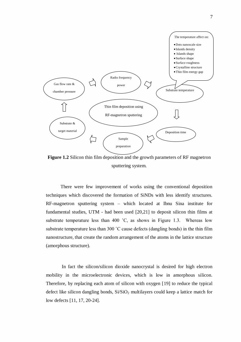
affected by the different growth parameters such as substrate temperature as shows in
Fig 1.2. However by changing the substrate temperature different nanodots
diameter, islands density, islands shape, surface roughness, crystalline structure and
optical properties could be obtained. It is essential to precise the size of the
nanoparticles, their density, and surface morphology, as the emission in visible scope
is clearly showed by a quantum confinement. Widely, the fabrication system applied
these values and the reduction of nanodots size follow by energy gap increasing
[17,18].
Silicon
Crystalline Silicon Amorphous Silicon
Porous Silicon
Nanocrystalline
Silicon
Poly Crystalline Si
Silicon
Hydrogenated
amorphous silicon
7
Figure 1.2 Silicon thin film deposition and the growth parameters of RF magnetron
sputtering system.
There were few improvement of works using the conventional deposition
techniques which discovered the formation of SiNDs with less identify structures.
RF-magnetron sputtering system – which located at Ibnu Sina institute for
fundamental studies, UTM - had been used [20,21] to deposit silicon thin films at
substrate temperature less than 400 ˚C, as shows in Figure 1.3. Whereas low
substrate temperature less than 300 ˚C cause defects (dangling bonds) in the thin film
nanostructure, that create the random arrangement of the atoms in the lattice structure
(amorphous structure).
In fact the silicon/silicon dioxide nanocrystal is desired for high electron
mobility in the microelectronic devices, which is low in amorphous silicon.
Therefore, by replacing each atom of silicon with oxygen [19] to reduce the typical
defect like silicon dangling bonds, Si/SiO2 multilayers could keep a lattice match for
low defects [11, 17, 20-24].
Radio frequency
power
Substrate temperature
Deposition time
Sample
preparation
Substrate &
target material
Gas flow rate &
chamber pressure
Thin film deposition using
RF-magnetron sputtering
system
The temperature affect on:
Dots nanoscale size
Islands density
Islands shape
Surface shape
Surface roughness
Crystalline structure
Thin film energy gap

8
Figure 1.3 The literature survey of radio frequency magnetron sputtering.
This study is involved which will result in quality of the SiNDs fabrication on
different substrates. The effect of temperature, chamber pressure, gas flow rate, and
RF-power on structural, optical and electrical properties of SiNDs growth has been
given attention so far. SiNDs deposited in plasma excitation radio frequency also
depend on these parameters. So by varying these parameters, the corresponding
structural and optical properties are expected to be significantly improved [7].
Therefore, to obtain silicon thin film with a high crystalline structure and high
surface roughness, it is proposed to increase the substrate temperature until 500 ˚C or
more.
Nucleation is a random process; in which the number of nuclei formed in a
fixed period of times is a random quantity and is subject to statistical laws.
However, the average values can be calculated and are subject to the kinetic theory
of nucleation. This research has been done to compare the simulation results with
the experimental works and confirm the classical theory of nucleation and growth
mode of Volmer- Weber. The formation of SiNDs can be predicted using a simple
model of the islands growth, where the atoms or vapours diffuse to each other
0
200
400
600
800
1000
1200
Tem
per
ature
(˚C
)
Deposition temperature
Annealing temperature

9
followed by agglomeration that form the nuclei of new phase. Thus, this research
describes the nucleation and growth of silicon nanodots for the vapour/liquid
transition with detailed analysis of parameters deduced from the theory and
experimental [25].
1.3 Research Objectives
The objectives of this research as to:
1. Reestablish the simulation works in order to confirm the classical theory of
nucleation and growth mode of Volmer- Weber.
2. Determine the optimum growth parameters of SiNDs and Si/SiO2 interface
for HVC system (deposition time, substrate temperature, gas flow rate, gas
pressure, and radio frequency power), as well as modify the HVC system.
3. Characterize silicon thin film structural properties of surface roughness and
nanndots size using AFM measurements follow by SEM measurement, and
determine the silicon atomic percentage that has deposit on the substrate by
used EDX measurements.
4. Characterize the energy gap (optical properties) of silicon thin film using PL
measurement to confirm the reduction of nanodots size follow by energy gap
increasing.
5. Characterize the grain (nanocrystal) size and silicon thin film crystalline
structure using XRD measurements.
10
1.4 Scope of the Study
This research explains the theoretical and simulation procedure of
heterogeneous nucleation. The simulation work represents the nucleation and growth
theory, including the transition from liquid-solid phase, also to prove the appearance
changing for net energy and nuclei size. The simulation program is conducted using
Microsoft Visual Basic 6.0 professional. As well as to determine the calculated
parameters using a computer programe are designed for a dome-like nucleus
assumed in Volmer-Weber growth theory.
Recently self-assembly technique to fabricate SiNDs is experimentally
carrying out by using radio frequency magnetron sputtering system for future
nanodevice applications. In this research, the quartz SiO2, corning glass (7059), and
silicon wafer have been chosen as substrates. Therefore, the experimental conditions
are identified at high substrate temperature of 600 ˚C in order to create silicon thin
film with high crystalline structure. Consequently, this deposition process is
performed using different growth parameters (deposition time, substrate temperature,
gas flow rate, gas pressure, and radio frequency power). SiNDs structural properties
are measured using AFM, EDX, SEM and XRD equipments following by optical
properties using PL measurement to calculate the energy gap of silicon thin film.

11
1.5 Significance of the Study
This study is essential to enhance the understanding of SiNDs growth
mechanism and its properties. The possibility to form a semiconductor thin film on
the surface of the glass substrates open a new aspect in understanding the structure,
electrical and optical properties of thin films. However these properties are attracting
researchers to fabricate various structural properties which are absolutely unlike the
naturally accessible properties [5].
Thin film deposition technique is adding new commercial devices and
allowing further characteristic in fabrication. Therefore it is a promising to improve
the devices utility and also keep the possessions materials wastes by the conventional
fabrication methods. In addition the quantum confinement of charge carriers
improves the field of nanostructure as influences the properties of materials. The key
to convergence the computing, communications and consumer electronics is the
optical, magnetic and electronic properties of thin films. It is apparent that thin film
has an important function to influence humanity in the future [5].
Recently, research related to Si nanostructure has been given consideration
and continuing trend towards integration of microelectronics and optoelectronics
devices. However, bulk Si has an indirect band-gap structure that limited its
application in optoelectronics for a very long time, due to the lower luminescence
efficiency [27]. Silicon becomes the preferred material for single-electron and
quantum electronic devices due to its unique structure, electrical and optical
properties. Recently SiNDs applications in electronics device is recommended and
agreed by the design of single memory and other devices requires the coulomb
blockade effect [16].

143
REFRENCES
1. Bryant, G.W. and G. Solomon, Optics of quantum dots and wires. 2005:
Artech House.
2. Ternon, F. Gourbilleau, R. Rizk, and C. Dufour, Si/SiO2 multilayers:
synthesis by reactive magnetron sputtering and photoluminescence emission.
Physica E: Low-dimensional Systems and Nanostructures, 2003. 16(3-4): p.
517-522.
3. Mizuta, H. and S. Oda, Bottom-up approach to silicon nanoelectronics.
Microelectronics Journal, 2008. 39(2): p. 171-176.
4. Zahi, H. Vergnes, B. Caussat, A. Estève, M. Djafari Rouhani, P. Mur, P.
Blaise, and E. Scheid, Towards multiscale modeling of Si nanocrystals
LPCVD deposition on SiO2: From ab initio calculations to reactor scale
simulations. Surface and Coatings Technology, 2007. 201(22-23): p. 8854-
8858.
5. SreeHarsha, Principles of physical vapor deposition of thin films. 2006:
Elsevier.
6. Cha, G. Kim, H.J. Doerr, and R.F. Bunshah, Effects of activated reactive
evaporation process parameters on the microhardness of polycrystalline
silicon carbide thin films. Thin Solid Films, 1994. 253(1-2): p. 212-217.
7. Yoo, C.S., Semiconductor manufacturing technology. 2008: World Scientific.
8. Henini, A. Patanè, A. Polimeni, A. Levin, L. Eaves, P.C. Main, and G. Hill,
Electrical and optical properties of self-assembled quantum dots.
Microelectronics Journal, 2002. 33(4): p. 313-318.
9. Sirenko, R. Fox, I.A. Akimov, X. Xi, S. Ruvimov, and Z. Liliental-Weber, In
situ Raman scattering studies of the amorphous and crystalline Si
nanoparticles. Solid State Communications, 2000. 113(10): p. 553-558.

144
10. Baron, T., F. Martin, P. Mur, C. Wyon, and M. Dupuy, Silicon quantum dot
nucleation on Si3N4, SiO2 and SiOxNy substrates for nanoelectronic devices.
Journal of Crystal Growth, 2000. 209(4): p. 1004-1008.
11. Gourbilleau, P. Voivenel, X. Portier, and R. Rizk, A novel method for the
deposition of Si-SiO2 superlattices. Microelectronics Reliability, 2000. 40(4-
5): p. 889-892.
12. Sun, and H.C. Kang, Synthesis and characterization of self-assembled ZnO
nano-dots grown on SiNx/Si(001) substrates by radio frequency magnetron
sputtering. Thin Solid Films, 2010. 518(22): p. 6522-6525.
13. S. Sakrani, F.A. Idrees, Z. Othaman, and A.K. Ismail, The Growth
Mechanism of Silicon Nanodots Synthesized by Sputtering Method. AIP
Conference Proceedings, 2011. 1341(1): p. 109-113.
14. Lopez Villanueva, J.A. Jimenez Tejada, A. Palma, S. Rodriguez Bolivar, and
J.E. Carceller. A simple model to analyze electron confinement and trapping
in silicon nanodots. in Electron Devices, 2005 Spanish Conference on. 2005.
15. Teo, X.H. Sun, Silicon-Based Low-Dimensional Nanomaterials and
Nanodevices. Chemical Reviews, 2007. 107(5): p. 1454-1532.
16. Xiao, S. Huang, J. Zheng, G. Xie, and Y. Xie, Optical characteristics of
Si/SiO2 multilayers prepared by magnetron sputtering. Microelectronic
Engineering, 2009. 86(11): p. 2342-2346.
17. Huang, Z. Xia, H. Xiao, J. Zheng, Y. Xie, and G. Xie, Structure and property
of Ge/Si nanomultilayers prepared by magnetron sputtering. Surface and
Coatings Technology, 2009. 204(5): p. 558-562.
18. Jung, Y.M. Jung, L.R. Shaginyan, and J.G. Han, Polycrystalline Si thin film
growth on glass using pulsed d.c. magnetron sputtering. Thin Solid Films,
2002. 420-421: p. 429-432.
19. Lewis, B. and J.C. Anderson, Nucleation and growth of thin films. 1978:
Academic Press.
20. L.Qie Jie, 2008, Silicon self-assembled nanodots prepared using radio
frequency magnetron sputtering, Master Thesis,Universiti Teknologi
Malasyia, Skudai.
21. Yeong Wai Woon, 2007, The formation structural and optical properties of
silicon nanocrystals embedded in silicon dioxide, Master Thesis, Universiti
Teknologi Malaysia, Skudai.

145
22. Charvet, R. Madelon, F. Gourbilleau, and R. Rizk, Ellipsometric
spectroscopy study of photoluminescent Si/SiO2 systems obtained by
magnetron co-sputtering. Journal of Luminescence, 1998. 80(1-4): p. 257-
261.
23. Ternon, F. Gourbilleau, X. Portier, P. Voivenel, and C. Dufour, An original
approach for the fabrication of Si/SiO2 multilayers using reactive magnetron
sputtering. Thin Solid Films, 2002. 419(1-2): p. 5-10.
24. Li, X.L. Wu, D.S. Hu, Y.M. Yang, T. Qiu, and J.C. Shen, Splitting of X-ray
diffraction peak in (Ge:SiO2)/SiO2 multilayers. Solid State Communications,
2004. 131(1): p. 21-25.
25. Aliberti, S.K. Shrestha, R. Teuscher, B. Zhang, M.A. Green, and G.J.
Conibeer, Study of silicon quantum dots in a SiO2 matrix for energy selective
contacts applications. Solar Energy Materials and Solar Cells, 2010. 94(11):
p. 1936-1941.
26. Xia, Z. and S. Huang, Structural and photoluminescence properties of silicon
nanocrystals embedded in SiC matrix prepared by magnetron sputtering.
Solid State Communications, 2010. 150(19-20): p. 914-918.
27. Kondo, T. Ueyama, E. Ikenaga, K. Kobayashi, A. Sakai, M. Ogawa, and S.
Zaima, Formation of high-density Si nanodots by agglomeration of ultra-thin
amorphous Si films. Thin Solid Films, 2008. 517(1): p. 297-299.
28. Ruzmetov, Y. Seo, L.J. Belenky, D.M. Kim, X. Ke, H. Sun, V.
Chandrasekhar, C.B. Eom, M.S. Rzchowski, and X. Pan, Epitaxial magnetic
perovskite nanostructures. Advanced Materials, 2005. 17(23): p. 2869-2872.
29. Ignac Capek, Slovak Academy of Sciences, Dúbravská cesta 9, Bratislava,
Slovakia, Chapter 1 Nanotechnology and nanomaterials, in Studies in
Interface Science, I. Capek, Editor. 2006, Elsevier. p. 1-69.
30. Diener, D. Kovalev, G. Polisski, and F. Koch, Luminescence properties of
two-photon excited silicon nanocrystals. Optical Materials, 2001. 17(1-2): p.
117-120.
31. Zhang, S. Shrestha, S.J. Huang, P. Aliberti, M.A. Green, and G. Conibeer,
Structural studies of multilayered Ge nanocrystals embedded in matrix
fabricated using magnetron sputtering. Energy Procedia, 2010. 2(1): p. 243-
250.

146
32. Teo, X.H. Sun, T.F. Hung, X.M. Meng, N.B. Wong, and S.T. Lee, Precision-
Cut Crystalline Silicon Nanodots and Nanorods from Nanowires and Direct
Visualization of Cross Sections and Growth Orientations of Silicon
Nanowires. Nano Letters, 2003. 3(12): p. 1735-1737.
33. A. Biswas, S. Bayer, A. Biris, T. Wang, E. Dervishi, F. Faupel, Advances in
top–down and bottom–up surface nanofabrication: Techniques, applications
and future prospects, Vol 170, Issues 1–2, 15 January 2012, Pages 2–27
34. Li, S.H. Chen, and H.L. Chen, Thermal-flow techniques for sub-35nm
contact-hole fabrication using Taguchi method in electron-beam lithography.
Microelectron. Eng., 2009. 86(11): p. 2170-2175.
35. Guo, E. Leobandung, L. Zhuang, and S.Y. Chou, Fabrication and
characterization of room temperature silicon single electron memory. Journal
of Vacuum Science & Technology B: Microelectronics and Nanometer
Structures, 1997. 15(6): p. 2840-2843.
36. Moliton, Solid-State Physics for Electronics. 2009: John Wiley & Sons.
37. Harrison, Quantum wells, wires, and dots: theoretical and computational
physics. 2000: John Wiley & Sons.
38. Schmid, G., Nanoparticles: from theory to application. 2004: Wiley-VCH.
39. Fox, Optical properties of solids. 2010: Oxford University Press.
40. Germanenko, S. Li, S.J. Silvers, and M.S. El-Shall, Characterization of
silicon nanocrystals and photoluminescence quenching in solution.
Nanostructured Materials, 1999. 12(5-8): p. 731-736.
41. Yu, X. Wang, W. Lu, S. Wang, Y. Bian, and G. Fu, Effects of substrate
temperature on microstructural and photoluminescent properties of
nanocrystalline silicon carbide films. Physica B: Condensed Matter, 2010.
405(6): p. 1624-1627.
42. Nayfeh, L. Mitas, Silicon Nanoparticles: New Photonic and Electronic
Material at the Transition Between Solid and Molecule, in Nanosilicon, K.
Vijay, Editor. 2008, Elsevier: Amsterdam. p. 1-78.
43. Eberl, O.G. Schmidt, O. Kienzle, and F. Ernst, Preparation and optical
properties of Ge and C-induced Ge quantum dots on Si. Thin Solid Films,
2000. 373(1-2): p. 164-169.
44. Chiquito, Y.A. Pusep, S. Mergulhão, J.C. Galzerani, and N.T. Moshegov,
Investigation of the InAs/GaAs self-assembled quantum dots using the
147
relationship between the capacitance and the density of states. Physica E:
Low-dimensional Systems and Nanostructures, 2001. 9(2): p. 321-325.
45. Dolino, D. Bellet, Variations in the lattice parameter of porous silicon
produced by wetting and vapour adsorption. Thin Solid Films, 1995. 255(1-
2): p. 132-134.
46. Charvet, R. Madelon, R. Rizk, B. Garrido, O. González-Varona, M. López,
A. Pérez-Rodríguez, and J.R. Morante, Substrate temperature dependence of
the photoluminescence efficiency of co-sputtered Si/SiO2 layers. Journal of
Luminescence, 1998. 80(1-4): p. 241-245.
47. Rebohle, J. von Borany, W. Skorupa, I.E. Tyschenko, and H. Fröb,
Photoluminescence and electroluminescence investigations at Ge-rich SiO2
layers. Journal of Luminescence, 1998. 80(1-4): p. 275-279.
48. Ma, L. Wang, K. Chen, W. Li, L. Zhang, Y. Bao, X. Wang, J. Xu, X. Huang,
and D. Feng, Blue light emission in nc-Si/SiO2 multilayers fabricated using
layer by layer plasma oxidation. Journal of Non-Crystalline Solids, 2002.
299-302(Part 1): p. 648-652.
49. Crupi, D. Corso, S. Lombardo, C. Gerardi, G. Ammendola, G. Nicotra, C.
Spinella, E. Rimini, and M. Melanotte, Memory effects in MOS devices based
on Si quantum dots. Materials Science and Engineering: C, 2003. 23(1-2): p.
33-36.
50. Xiaoli, S. Yi, G. Shulin, Z. Jianmin, Z. Youdou, S. Kenichi, I. Hiroki, and H.
Toshiro, Effects of interface traps in silicon-quantum-dots-based memory
structures. Physica E: Low-dimensional Systems and Nanostructures, 2000.
8(2): p. 189-193.
51. Puglisi, S. Lombardo, G. Ammendola, G. Nicotra, and C. Gerardi, Imaging of
Si quantum dots as charge storage nodes. Materials Science and Engineering:
C, 2003. 23(6-8): p. 1047-1051.
52. Lombardo, S. Coffa, C. Bongiorno, C. Spinella, E. Castagna, A. Sciuto, C.
Gerardi, F. Ferrari, B. Fazio, and S. Privitera, Correlation of dot size
distribution with luminescence and electrical transport of Si quantum dots
embedded in SiO2. Materials Science and Engineering B, 2000. 69-70: p. 295-
298.

148
53. Chen, Y. Ren, R.l. Xiong, Y.y. Zhao, and M. Lu, Modulation of the
photoluminescence of Si quantum dots by means of CO2 laser pre-annealing.
Applied Surface Science, 2010. 256(16): p. 5116-5119.
54. Reinig, B. Selle, F. Fenske, W. Fuhs, V. Alex, and M. Birkholz, Highly
oriented growth of polycrystalline silicon films on glass by pulsed magnetron
sputtering. Vol. 20. 2002: AVS. 2004-2006.
55. Torchynska, Photoluminescence of Si nanocrystallites in different types of
matrices. Journal of Non-Crystalline Solids, 2006. 352(23-25): p. 2484-2487.
56. Torchynska, T., J. Aguilar-Hernandez, M. Morales Rodriguez, C. Mejia-
Garcia, G. Contreras-Puente, F.G. Becerril Espinoza, B.M. Bulakh, L.V.
Scherbina, Y. Goldstein, A. Many, and J. Jedrzejewski, Comparative
investigation of photoluminescence of silicon wire structures and silicon
oxide films. Journal of Physics and Chemistry of Solids, 2002. 63(4): p. 561-
568.
57. Papon, J. Leblond, and P.H.E. Meijer, The physics of phase transitions:
concepts and applications. 2006: Springer-Verlag.
58. Myerson, R. Ginde, Crystals, crystal growth, and nucleation, in Handbook of
Industrial Crystallization (Second Edition), S.M. Allan, Editor. 2002,
Butterworth-Heinemann: Woburn. p. 33-65.
59. Spaepen, Homogeneous Nucleation and the Temperature Dependence of the
Crystal-Melt Interfacial Tension, in Solid State Physics, E. Henry and T.
David, Editors. 1994, Academic Press. p. 1-32.
60. Salk, D.E. Hagen, and C.K. Lutrus, Propensity rule in homogeneous
nucleation processes. Chemical Physics Letters, 1988. 146(6): p. 605-608.
61. Rao, B.J. Berne, Nucleation in finite systems: Theory and computer
simulation. Astrophysics and Space Science, 1979. 65(1): p. 39-46.
62. Mullin, Nucleation, in Crystallization (Fourth Edition). 2001, Butterworth-
Heinemann: Oxford. p. 181-215.
63. Cao, Nanostructures & nanomaterials: synthesis, properties & applications.
2004: Imperial College Press.
64. Idrees, F.A., S. Sakrani, and Z. Othaman, Formation and Characterization of
Silicon Self-assembled Nanodots. AIP Conference Proceedings, 2011.
1341(1): p. 324-327.

149
65. Priester, C. and M. Lannoo, Growth aspects of quantum dots. Current
Opinion in Solid State and Materials Science, 1997. 2(6): p. 716-721.
66. Le Thanh, V. and V. Yam, Superlattices of self-assembled Ge/Si(0 0 1)
quantum dots. Applied Surface Science, 2003. 212-213: p. 296-304.
67. Larsson, A. Elfving, P.O. Holtz, G.V. Hansson, and W.X. Ni, Luminescence
study of Si/Ge quantum dots. Physica E: Low-dimensional Systems and
Nanostructures, 2003. 16(3-4): p. 476-480.
68. Talalaev, G.E. Cirlin, A.A. Tonkikh, N.D. Zakharov, P. Werner, U. Gösele,
J.W. Tomm, and T. Elsaesser, Miniband-related 1.4-1.8 [mu]m
Luminescence of Ge/Si Quantum Dot Superlattices, in Handbook of Self
Assembled Semiconductor Nanostructures for Novel Devices in Photonics
and Electronics, H. Mohamed, Editor. 2008, Elsevier: Amsterdam. p. 324-
345.
69. Müller, O. Kirfel, A. Rastelli, H. von Känel, and D. Grützmacher, Successful
shape-preservation of Ge-clusters during Si-coverage at low temperature.
Materials Science and Engineering B, 2003. 101(1-3): p. 142-145.
70. Zhou, R.A. Johnson, and H.N.G. Wadley, Vacancy formation during vapor
deposition. Acta Materialia, 1997. 45(11): p. 4441-4452.
71. Wood, Thin-film optical filters: 3rd edition : H.A. Macleod; Thin Film Centre
Inc., Tuscon, Arizona & University of Arizona, USA, Institute of Physics
Publishing, 2001, 672pp, ISBN 0-7503-0688-2. Optics and Lasers in
Engineering, 2002. 37(6): p. 673-674.
72. Palmero, H. Rudolph, and F.H.P.M. Habraken, One-dimensional analysis of
the rate of plasma-assisted sputter deposition. Vol. 101. 2007: AIP. 083307.
73. Margaritondo, R. Joynt, M. Onellion, and A.V. Society, High Tc
superconducting thin films, devices, and applications, Atlanta, GA, 1988.
1989: American Institute of Physics.
74. Bach, D. Krause, Thin films on glass. 1997: Springer.
75. Shi, Functional thin films and functional materials: new concepts and
technologies. 2003: Springer.
76. Mattox, Physical Sputtering and Sputter Deposition (Sputtering), in
Handbook of Physical Vapor Deposition (PVD) Processing (Second Edition).
2010, William Andrew Publishing: Boston. p. 237-286.

150
77. Mattox, Film Characterization and Some Basic Film Properties, in
Handbook of Physical Vapor Deposition (PVD) Processing. 1998, William
Andrew Publishing: Westwood, NJ. p. 569-615.
78. Mattox, Vacuum Evaporation and Vacuum Deposition, in Handbook of
Physical Vapor Deposition (PVD) Processing. 1998, William Andrew
Publishing: Westwood, NJ. p. 288-342.
79. Behrisch, W. Eckstein, Sputtering by particle bombardment: experiments and
computer calculations from threshold to MeV energies. 2007: Springer.
80. Behrisch, K. Wittmaack, Sputtering by particle bombardment III:
characteristics of sputtered particles, technical applications. 1991: Springer-
Verlag.
81. Hattum, A.P. , H.R. W. M. Arnoldbik, and F.H.P.M. Habraken, Distinct
processes in radio-frequency reactive magnetron plasma sputter deposition
of silicon suboxide films. Journal of applied physics, 2007(124505): p. 102.
82. Licari, L.R. Enlow, Thin Film Processes, in Hybrid Microcircuit Technology
Handbook (Second Edition), J.L. James and R.E. Leonard, Editors. 1998,
William Andrew Publishing: Westwood, NJ. p. 63-103.
83. Kodigala, K. Subba Ramaiah, Structural Properties of I-III-VI2 Absorbers, in
Thin Films and Nanostructures. 2010, Academic Press. p. 115-194.
84. Benchiheb, M.S. Aida, and N. Attaf, Plasma optical emission spectroscopy
diagnostic during amorphous silicon thin films deposition by Rf sputtering
technique. Materials Science and Engineering: B, 2010. 172(2): p. 191-195.
85. Allen, D.J. Tildesley, Computer Simulation of Liquids. 1989: Oxford
University Press, USA.
86. S. Sakrani, L.Qie.Jie, Yussof Wahab, The formation of nanoscale clusters –
nanofilms / quantum dots predicted using a capillary model of nucleation.
Journal of Fundamental Sciences, 2005: p. 23-34.
87. Madras, B.J. McCoy, Temperature effects on the transition from nucleation
and growth to Ostwald ripening. Chemical Engineering Science, 2004.
59(13): p. 2753-2765.
88. Qin, Bubble formation in lattice Boltzmann immiscible shear flow. The
Journal of Chemical Physics, 2007. 126(11): p. 114506-5.

151
89. M. Ali, Growth and study of magnetostrictive FeSiBC thin films for device
applications, in Department of Physics & Astronomy. 1999, The University
of Sheffield.
90. Birkholz, P.F. Fewster, and C. Genzel, Thin film analysis by X-ray scattering.
2006: Wiley-VCH.
91. Birkholz, Principles of X-ray Diffraction, in Thin Film Analysis by X-Ray
Scattering. 2006, Wiley-VCH Verlag GmbH & Co. KGaA. p. 1-40.
92. Cullity, S.R. Stock, Elements of x-ray diffraction. 2001: Prentice Hall.
93. Samavati, A., F. Aldaw, S.K. Ghoshal, Z. Othaman, and S. Sakrani, Light
emitting germanium and silicon nanoislands grown by RF magnetron
sputtering. Journal of Ovonic Research. 8(3): p. 65-72.
94. Chen, Z. Jiao, M.H. Wu, C.H. Shek, C.M.L. Wu, and J.K.L. Lai,
Microstructural evolution of oxides and semiconductor thin films. Progress in
Materials Science, 2011. 56(7): p. 901-1029.
95. Hasegawa, M. Sakata, T. Inokuma, and Y. Kurata, Structural change of
polycrystalline silicon films with different deposition temperature. Journal of
applied physics, 1999. 85(7): p. 3844-3849.
96. Setyawan, M. Shimada, Y. Imajo, Y. Hayashi, and K. Okuyama,
Characterization of particle contamination in process steps during plasma-
enhanced chemical vapor deposition operation. Journal of Aerosol Science,
2003. 34(7): p. 923-936.
97. Mattox, 5 - Vacuum Evaporation and Vacuum Deposition, in Handbook of
Physical Vapor Deposition (PVD) Processing. 1998, William Andrew
Publishing: Westwood, NJ. p. 288-342.
98. De Los Santos, D. Lee, J. Seo, F.L. Leon, D.A. Bustamante, S. Suzuki, Y.
Majima, T. Mitrelias, A. Ionescu, and C.H.W. Barnes, Crystallization and
surface morphology of Au/SiO2 thin films following furnace and flame
annealing. Surface Science, 2009. 603(19): p. 2978-2985.
99. Chen, L. Lai, C.H. Shek, and H.D. Chen, Production of amorphous tin oxide
thin films and microstructural transformation induced by heat treatment.
Applied Physics A: Materials Science & Processing, 2005. 81(5): p. 1073-
1076.

152
100. Sun, H.C. Kang, Synthesis and characterization of self-assembled ZnO nano-
dots grown on SiNx/Si(001) substrates by radio frequency magnetron
sputtering. Thin Solid Films. 518(22): p. 6522-6525.
101. Germanenko, Effect of atmospheric oxidation on the electronic and
photoluminescence properties of silicon nanocrystals. Pure Appl. Chem,
2000, Vol. 72, Nos. 1–2, pp. 245–255.
102. Chen, H. Chang, A.-T. Chou, T.-M. Hsu, P.-S. Chen, Z. Pei, and L.-S. Lai,
Optical properties of stacked Ge/Si quantum dots with different spacer
thickness grown by chemical vapor deposition. Applied Surface Science,
2004. 224(1-4): p. 148-151.
103. Gfroerer, Photoluminescence in Analysis of Surfaces and Interfaces, in
Encyclopedia of Analytical Chemistry. 2006, John Wiley & Sons, Ltd.
104. Kenyon, P. Trwoga, C.W. Pitt, and G. Rehm, The origin of
photoluminescence from thin films of silicon-rich silica. Journal of applied
physics, 1996. 79(12): p. 9291-9300.
105. Ma, L. Wang, K. Chen, W. Li, L. Zhang, Y. Bao, X. Wang, J. Xu, X. Huang,
and D. Feng, Blue light emission in nc-Si/SiO2 multilayers fabricated using
layer by layer plasma oxidation. Journal of Non-Crystalline Solids, 2002.
299-302, Part 1(0): p. 648-652.
106. Chen, Z. Ma, X. Huang, J. Xu, W. Li, Y. Sui, J. Mei, and D. Zhu,
Comparison between light emission from Si/SiNX and Si/SiO2 multilayers:
role of interface states. Journal of Non-Crystalline Solids, 2004. 338-340(0):
p. 448-451.
107. Zheng, Y.H. Zuo, W. Wang, Y.L. Tao, C.L. Xue, B.W. Cheng, and Q.M.
Wang, Efficient emission and energy transfer in Si/Er-Si-O multilayer
structure. Materials Research Bulletin, 2011. 46(2): p. 262-265.
108. Fafard, Ventra, Massimiliano, Evoy, Stephane Heflin, James, Quantum-
Confined Optoelectronic Systems Introduction to Nanoscale Science and
Technology. 2004, Springer US. p. 443-483.