Embed Size (px)
Citation preview

Abstract-A new modification of the MNOS transistor results in sig- nificant advantages. It combines a depletion-mode channel with elec- trically separate electrodes over the memory portion and the fixed threshold portion of a step-gate device. This eliminates read disturb during interrogation; therefore, much longer retention is now possible. It also decreases access time within an LSI array. For block-written EAROM’s, a new form of dynamic inhibit makes memory array isola- tion unnecessary. These and other improvements obtained with this structure do not require new processes or a significant increase in size.
INTRODUCTION
T HE MOST FREQUENTLY USED technology for MNOS- LSI memory circuits, involving pchannel technology and
epi-junction isolation [ 11, has by now reached a high level of development. The limitations in this line of approach are apparent. The use of p-channel technology limits the operat- ing time. In addition, there is an irreducible conflict between retention [2] and access time. In order to minimize read dis- turb [2] and maximize retention, the voltage placed on the gate of the MNOS memory transistor should result in a mini- mum difference between stored threshold voltage and applied voltage. But it should be made as large as possible to reduce access time. A typical compromise in recently designed EAROM’s [3] results in a retention (at constant read) of 30 years and an access time increment due to the memory tran- sistor alone of about 500 ns. The limitation is more severe in RAM [4] circuits, where the need for access times below 1-ps limits the constant read retention to a few hours. A similar limitation exists with respect to endurance [2]. It is possible to increase endurance by decreasing the write field [2]. How- ever, in order to obtain the necessary output drive from the memory transistor, the read conditions must remain un- changed. With write and read voltage closer to each other in value, read disturb is increased and retention is reduced. The best that can be expected from present EAROM’s is an endur- ance of 108-109 [3], and from RAM circuits 1010-1012 [4]. In addition, the need for writing words independently of each other introduces the requirements of electrically separating the substrates of the peripheral circuits from the substrate of the memory array. This is accomplished with the help of an epitaxial junction isolated laterally by diffused walls, at the cost of two additional masking steps, and the yield losses associated with large junctions and the potential for emitter- collector-type short circuits.
Some of these problems were addressed in a recent paper by Schuermeyer and Young [5] and in an earlier paper by Tickle
Manuscript received December 12, 1978;revised March 15, 1979. The author was with Sperry Research Center, Sudbury, MA 01776.
He is now with Hewlett-Packard Laboratories, Palo Alto, CA 94304.
[9]. In it they proposed the use of present MNOS memory dielectrics in conjunction with rt-channel techrdogy. This would at once reduce th.e accws rime of the circuit due to the higher mobility of the electrons which are the carriers in this technology. In addition, they find that the us’e of the step- gate structure [6] with its fhed thresholkl enhancement gate characteristics in series, makes the use of -the depletion mode possible within a memory array. When used within the struc- ture of a flip-flop memory cell, their approach makes special memory substrate isolation tmnecessary. Their NOVCID- VINRAM configuration also :introduces a form of dynamic inhibit, although the step gate makes substrate isolation necessary.
In the following pages an (extension ‘of Schuermeyer and Young’s concepts will be proposed. Specifically, it involves the separation of the single-gate electrode used in a standard step-gate structure into two electrodes with one covering only the fixed-threshold regions of the device and the other only the memory region. Since the electrode over the fixed- threshold gate controls all acees,s to the memory device, this new structure is called the gat.ed-access transistor. The gated- access transistor makes far reaching improvements possible in the MNOS-LSI memory circuit technology.
The use of separately gated access t’o a depletion MNOS memory device at once elimina1.es the conflict between mini- mum read disturb and minimum access time. Reading may now be accomplished withalut any voltage placed on the memory gate; thus there is no read disturb and the maximum retention for a given dielectric is obtained. This means that there are now hundreds of years of retention for slower writ- ing devices and at least thirty years of retention for devices with a 1-ps write pulsewidth. The access time now depends both on the voltage placed across the access gate of the memory transistor and the actual value of the threshold volt- age stored. In practice, the access time has been reduced by at least a factor of five. A similar decoupling of read and write voltage now permits the utilization of devices with higher endurance. This is possible because the absence of any read disturb facilitates the use of devices with low write voltage.
The gated-access transistor also facilitates writing a two- dimensional EAROM array on an LSI chip without the need for substrate isolation. Thus processing now can be done with a minimum of steps, simultaneously reducing cost and increas- ing yield. In one approach proposed here a standard low- voltage self-aligned gate nchannel process, modified by the addition of a silicon nitride layer, is all that is necessary. This makes it particularly easy to integrate EAROM’s within micro- processor chips.
The new structure also has advantages in an environment
0018-9383/80/0100-0266$00.75 0 1980 IEEE

WEGENER: THE GATED-ACCESS MNOS MEMORY TRANSISTOR 261
requiring radiation hardness. It provides chemical protec- tion during processing to preserve the inherent hardness of Aubuchon [7] process oxide gates; it also permits the use of source-drain protection in a radiation environment without any problems due to positive potentials.
All of these advantages are obtained at no or only slight penalties in bit density. Processes to realize the required structure are, aside from the standard self-aligned n-type pro- cess, a p-type process which includes a depletion-type load and a polysilicon layer, and an n-type process with similar features.
STRUCTURE OF GATED-ACCESS TRANSISTOR In order to make the depletion transistors proposed here
individually addressable within an array of memory transistors on the same chip, access gates have to be provided to separate both source and drain from common connections within the array. This is accomplished most simply within the framework of the step-gate transistor [ 6 ] . In such a device, the two fixed- threshold regions located on either side of the memory region are turned on only when an interrogation voltage is placed on the gate electrode. But in the present device it is only the fixed threshold portions that need to be turned on: the depletion-type memory portion is in a conducting state even when the applied gate voltage is zero. If, therefore, the gate electrodes over the fixed threshold portion of the step gates are separated from the electrode over the memory portion, reading can be accomplished while the memory dielectric is under zero bias.
In a process which includes a polysilicon layer, the cross section of such a transistor assumes the configuration shown in Fig. 1. The two polysilicon gate portions are connected to a separate aluminum line above the plane of the cross section shown.
A particularly simple realization of this concept can be found in the combination of the self-aligned silicon-gate n-channel process with the memory dielectrics that have already been developed for p-channel MNOS memory transis- tors. These dielectrics store charges after writing that are equivalent to negative threshold voltages. But negative thresh- old voltages will turn n-channel IGFET’s permanently on: they result in depletion transistors. The self-aligned silicon gates automatically provide the separate electrodes for the access gates. The memory dielectrics referred to here may be any of those established by experience in actual fabrication of p-channel devices. Typically, they have a thin oxide layer (from 8-30 A), and a nitride layer of about 500 A.
n-CHANNEL PROCESS FOR GATED-ACCESS TRANSISTOR A representative self-aligned polysilicon-gate process might
start with a high-resistivity (20 S2 * cm) slice of p-type bulk silicon. A field isolation thermal oxide layer of 5000 A is then grown, and the areas where source-drain junctions and gate regions will be formed are etched clean of oxide by standard photoresist masking techniques. Next, a 1000-8 gate oxide is grown, followed by a threshold controlling ion implant that will place boron atoms at the interface between the 1000-14 oxide and the silicon. This is performed to adjust the voltage of the fixed-threshold devices. Next, polysilicon is deposited,
”.TYPE SILICON’ POLYS~LICON DEPLETION LAYER
Fig. 1 . The gatedaccess depletion MNOS memory transistor.
IN
pTYPE SUBSTRATE
Fig. 2. Detail of MIS structure lateral to the polysilicon gate when “standard” process is used.
followed with a deposited oxide layer; and it is removed in such a way that it remains as the gate electrode over all tran- sistor regions and wherever it is used as a second layer inter- connect, but it is definitely removed over the regions where source-drain junctions and doped silicon interconnects are going to be formed. The required doping function is then per- formed by an n+ ion implantation. By a third photoresist step contact holes are defined in bulk and polysilicon. Finally, aluminum is evaporated and patterned by photoresist etching in order to form contacts with all device and. interconnect regions, and to provide, by itself, a third layer of interconnect. Inversion at the surface can be prevented by a reverse substrate bias provided by an external power supply, or by a pumped charge generator.
This process requires only a minor modification to form an MNOS memory transistor. After the source-drain junction doping has been performed, another photoresist step results in the formation of a slot across the gate electrodes of the fixed threshold structures formed in anticipation of this step. The gate dielectric is then removed to bare the silicon. Next the memory dielectric is deposited. The normal process sequence then resumes with the photoresist etching of the contact openings. Thus an MNOS-LSI process based on the n-channel self-aligned gate process only requires two additional steps over the standard sequence: a masking step to define the memory gate locations, and the nitride deposition to form the memory dielectric.
PROCESS MODIFICATION There is a small probability for the existence of a structural
weakness in the proposed embodiment of the gated-access concept. This might arise in the region of the MIS structure formed by the sidewall of the silicon-gate electrode, the deposited silicon nitride and the aluminum electrode (Fig. 2 ) . There are two possible problems: The first is due to the fact that this structure will also act as a memory dielectric with potential endurance problems; the other is related to micro- scopic inhomogeneities that might be generated at the poly- silicon sidewall surface and in the nitride layer deposited over

268 IEEE TRANSACTIONS ON ELECTROS CEV'ICES, VITI,. ED-27, NO. 1 , JANUARY 1980
n.TYPE SILICON'
(I-TYPE SUBSTRATE
Fig. 3. Detail of MIS structure lateral to the polysilicon gate when local oxidation is used.
it. Both could lead to premature dielectric breakdown. If, in fact, such behavior is found, a simple modification in the process could prevent this problem. Immediately following the formation of the fixed threshold dielectric, a 1 0 0 4 layer of silicon nitride is deposited over it. This layer can be re- moved preferentially by phosphoric acid, when the gate dielectric is removed for the self-aligned diffusion step. After the slot in the polysilicon electrode has been formed to define the area of the memory dielectric, the exposed silicon nitride layer is left untouched. Next, 2000 A of thermal oxide are grown over the bare polysilicon electrode sidewall. The nitride layer will shield the oxide exposed in the memory gate region from further oxidation. Successive removal of nitride and 1000 A of oxide will bare the silicon where a memory gate will be located, but it will still leave 1000 A of oxide over the poly- silicon gate. Deposition of the memory dielectric will increase the total thickness of dielectric over the sidewall of the poly- silicon gate electrode so that the projected problem areas are unlikely to develop (Fig. 3).
DEMONSTRATION OF ABSENCE OF READ DISTURB In order to prove the expected independence of a depletion-
type MNOS memory transistor from read disturb effects an n-channel transistor having the standard annular (enclosed drain) configuration was provided with a 200: 1 memory dielectric [ l ] . Then the transistor was connected to ground with its source, substrate, and gate leads. The drain lead was connected to a resistor (1 ki2 in most cases), and the resistor was connected to a positive power supply voltage VDD. The voltage drop VD between source and drain was directly dis- played on a digital voltmeter. With a separately measured value of the k' [2] of the transistor, V i could be used to calculate the instantaneous threshold voltage of the transistor from the applicable drain current equation. A plot of both threshold voltage extremes of the transistor versus time is shown in Fig. 4. These two threshold voltage levels were obtained with write pulses of 10 ps at +25 V. As can be seen, the data points fall on the straight lines of a plot typical for zero (gate) bias retention. The transistors have, however, been under constant interrogation since the drain supply maintained a current through the depletion channel. This current was proportional to both the drain voltage and the threshold volt- age. For the 24 h of the retention measurements, the transis- tor with the largest drain voltage and threshold voltage had about 8.5 mA of dc passing through it. Inspection of Fig. 4 indicates that, as least for the first five orders of magnitude of retention, there is no discernible effect of the drain voltage
.10 -9 I VO: +1.5V = 0 , 15.0V = a, t10,OV = a tW: IO.%, tRO - 1010,
Fig. 4. Retention under continuous read condition of n-channel MNOS transistor.
magnitude. Extrapollation to longer time periods results in a projected threshold. voltage window of 2 V after an elapse of 10" s or 300 years, under constant interrogation. A retention curve obtained from a p-c'hannel enhancement transistor with the same 200 :1 dielectric under zero bias indicates a some- what shorter retention and a somewhat changed slope. Both are consistent with an explanation involving a reduced positive potential at the silicon/dielectric interface of the n-channel device due to the bu:k voltage that must be dropped across the depletion region. It should be pointed out that in a normally interrogated MNOS transistor, the condition causing the least disturb would be reading under constant current conditions. Under these most benign operating conditions the retention of the p-channel enhancement version is lo3 s. Thus the gated-access depletion-type MNOS transistor increases reten- tion under operating conditions by seven orders of magnitude for the same dielectric.
REDUCTION OF ACCESS TIME In currently used step-gate versions of the enhancement
transistors incorporating MNOS memory gate dielectrics, the problem in circuit design lies in a balanced tradeoff between maximum gate voltage VG to reduce access time by obtaining a large output current from the MNOS memory device, and a minimum difference between gate voltage and threshold volt- age, in order to minimize read disturb and, therefore, to maxi- mize retention. In the gated-access transistor structure, this problem does not exist. The access gates can be driven as hard as available voltage can make it possible and, in addition, the zero bias on-voltage, which is proportional to the threshold voltage, is significiantly larger than the VG - V, designed into present LSI arrays. This can be demonstrated by a simplified calculation. Fig. 5(a) shows a representation of a step-gate transistor as three transistors in series, with a common gate electrode. Fig. 5(b) shows a representation of the gated-access transistor. The major difference lies in the separate leads for the fixed threshold devices and the memory device.
In the Appendix, calculations are made of the current out- put of the two compound structures shown in Fig. 5(a) and (b). These calculations are done under constant current con- ditions for the step-gate transistor and under typical operating

WEGENER: THE GATED-ACCESS MNOS MEMORY TRANSISTOR 2 69
V G O ' V G N
P
'Dl "D2
(a)
'GO VGN p I
vDD
'Dl
@) Fig. 5 . Comparison of schematic representations of (a) stepped-gate
transistor and (b) gated-access transistor.
'D2
TABLE I CALCULATED ACCESS TIMES
StcD Gate Gated A c c m
V m = - 2 5 0 0 ns 100 ns
VT, = - 10 145 ns 60 ns
conditions for the gated-access transistor. The calculated out- put is proportional to the drain conductance (which is set to the identical value for both transistor types) and the applied gate voltages to obtain the desired read output. The latter results in a factor a by which the drain conductance is multi- plied. When these current values are substituted into a simpli- fied charging time expression, a comparison of the access times for step-gate and gated-access transistors can be made. This is shown in Table I. This table indicates that access time for the low threshold voltage state is the slower of the two and is im- proved by a factor of five. The faster of the two is also im- proved, although not as drastically. This is an additional ad- vantage since now over the complete life of information stored, the average access time does not change by more than f 20 percent.
FACILITATION OF LOW WRITE VOLTAGE The relatively high write voltage of 25 to 30 V required by
typical MNOS transistor types constitutes a barrier for a wider application of MNOS transistors. Within a system, the high voltage leads to the need of more expensive and nonstandard power supplies, and, in the use and control of this high volt- age, to higher power dissipation. The high voltage require- ment leads to lower yields during chip manufacture, since fewer junctions and dielectrics can be expected to meet the acceptance specifications. Finally, high write voltages limit the number of write-erase cycles that a given MNOS transistor itself can endure without unacceptable changes in electrical characteristics.
10-4 10-2 100 1 02 104 106
RETENTION ( s i
0 : ZERO BIAS RETENTION + = CONSTANT VOLTAGE RETENTION x = CONSTANT CURRENT RETENTION
Fig. 6 . Retention of low-write-voltage MNOS transistor.
I 1 1 1 1 1 1 1 1 I l I I I 1 1 1 1 I 1 1 1 1 1 1 1 1 I 1 1 1 1 1 1 1 1 I 1 I
0 - . . . . m . 177E - 15 V. 100 ps
I I 1 1 1 1 0 1 I I lI11111 1 11111111 I 1 1 1 1 1 1 1 1 I I I l l
105 106 107 lo8 109 I1010
WRlTElERASE CYCLES
Fig. 7. Endurance of low-write-voltage MNOS transistor.
While it is quite feasible to make memory dielectrics with write voltages that are significantly lower, the read disturb on such devices would be very large, since read voltage and write voltage would now have nearly identical values. But since there is no read potential placed on the memory electrode of the gated-access transistor, it is now possible to use low write voltage MNOS transistors in practical applications.
The retention characteristics of such a device are shown in Fig. 6 . The transistor was written with a +15-V, 100-ps write pulse. The zero bias retention [2] equivalent to the retention under constant read condition in a gated access transistor can be extrapolated to about 3 X lo' s, or one year. More tradi- tional modes of interrogation, such as constant voltage on the memory gate or constant current through the device channel, result in retentions of the order of 0.3 and 2 s, respectively.
The low write voltage capability was obtained by a modifica- tion of the properties of the memory dielectric, not by making a standard memory dielectric thinner. The thickness of this modified dielectric was a typical 430 A. Thus the field across the memory dielectric is significantly lower than in standard devices. This is reflected in the write-erase cycling (endur- ance) data shown in Fig. 7. Clearly, there are only negligible changes after nearly 10" cycles. An unmodified device with equivalent writing or retention characteristics but written at 25 V would have shown significant changes in characteristics after 10' cycles.
Thus the gated-access transistor structure makes possible the
use of low write voltage MNOS transistors, which reduces system power supply and dissipation requirements, improves process yield, and increases product life.
BLOCK WRITING SCHEME FOR EAROM REQUIRING NO
ARRAY SUBSTRATE ISOLATION Many currently designed and operating EAROM’s using
MNOS memory transistors require a block erase step to initiate writing. That means, that in order to change information on a given memory LSI chip, all information on that chip has to be wiped out first. After erasure, the information is written into the array word by word. Assuming that the internal organiza- tion of the chip involved 36 words, the writing of a typical EAROM would take upwards of 37 ms. This same chip still needs array substrate isolation to permit the use of a positive erase potential.
The writing scheme made possible by the gated-access tran- sistor utilizes a single write line that is common to every bit. This single line lies only over dielectric material (memory or field isolation), and it never comes in contact with the silicon of the chip. In this way it can carry electrical signals of both positive and negative polarities. These are supplied from a driver off chip. Since the write signals are the only high- voltage signals needed, the technology for the circuit itself may be a standard, relatively low-voltage, self-aligned silicon- gate n-channel type.
The concept that makes this advance possible involves the use of the temporary absence or presence of equilibrium charge in a potential well. It uses the same phenomena that have been used in CCD arrays. In the context of writing gated- access devices, it is done in the following manner.
First, the transistor is written in such a way that its memory portion forms a deep potential well. This is accomplished by placing a negative write voltage on the writing gate (the alu- minum electrode over the memory portion of the transistor in Fig. 1). This will result in a negative-threshold voltage extreme when the access gate (the polysilicon electrodes over the fixed threshold portions of the transistor) is held at zero potential and when the substrate is also held at zero potential.
Next, the deep potential well is either filled or emptied by first placing the appropriate voltage on source and drain, and then turning on the access gate. A filled well is generated by placing a zero potential on source and drain. Then electrons enter the channel region of the memory portion to neutralize the positive charges stored in the dielectric (which is repre- sented by the large negative threshold voltage). An empty well is generated by withdrawing such electrons. This is accom- plished by placing a positive voltage equal to or slightly greater than the absolute magnitude of the threshold voltage of the memory region on the source and drain. Once the well condi- tion has been set, the access gate must be turned off before the source-drain potential is changed. The third step consists of placing a positive write voltage on the writing gate. If the well was filled with electrons they will be drawn into the dielectric, thus neutralizing the positive charge stored in the dielectric, at least in part. In this way the threshold voltage is made less negative and the potential well much shallower. If the well was empty the space-charge region in the silicon will act as
additional. dielectric. Therefore, for thle duration ofihe write pulse no change in threshold voltage is expected.
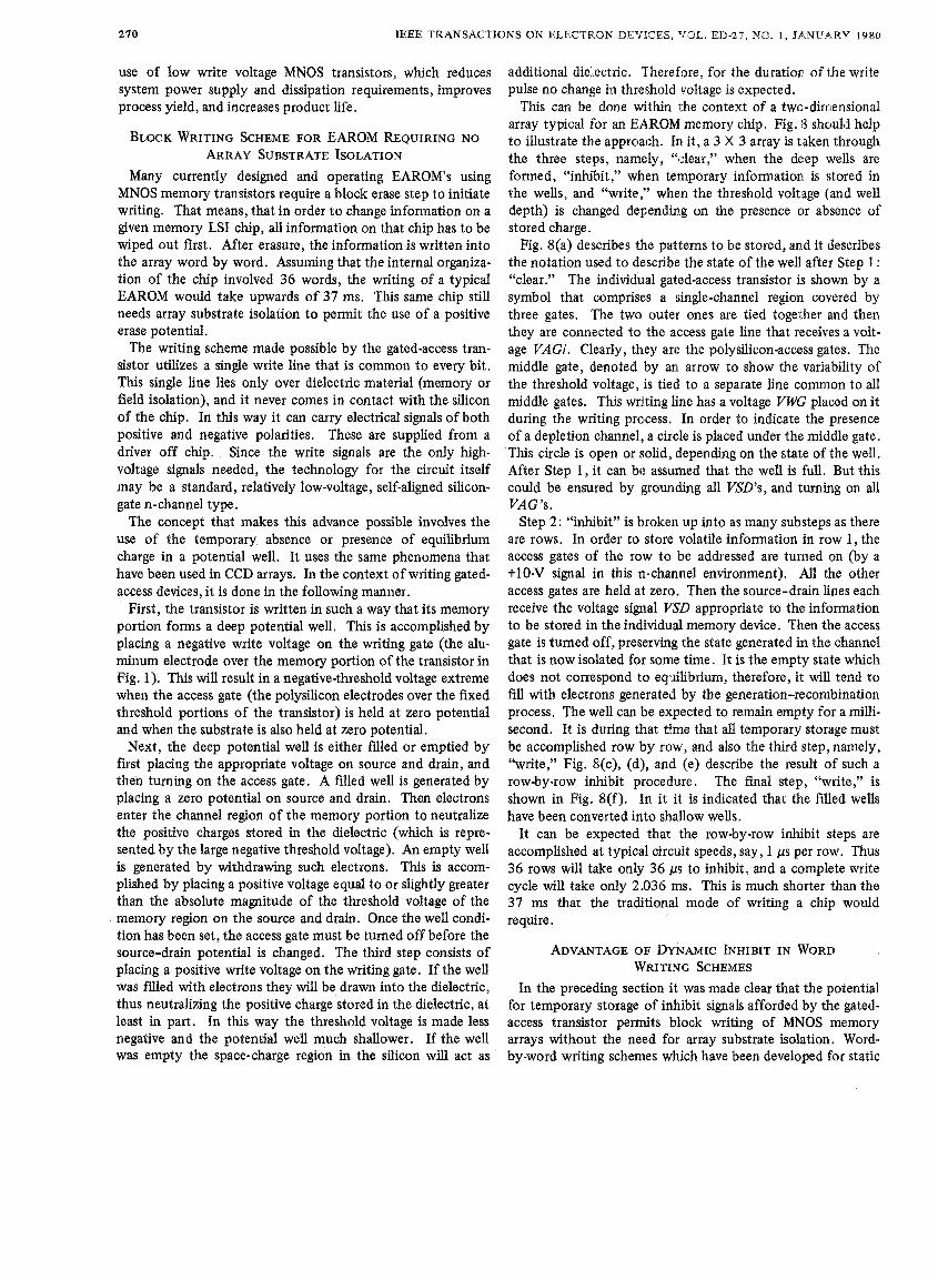
This can be done within rhe c0ntex.t of a two-dimensional array typical for an EA.ROM memory chip. Fig. 8 should help to illustrate the approach. In it, a 3 X 3 array is taken through the three steps, namely, “clear,” when the deep wells are formed, “inhibit,” when temporary informationl is stored in the wells, and “write,” whe,n the threshold voltage (:and well depth) is changed dependiag on the presence or ablsence of stored charge.
Fig. 8(a) describes the patterns to be stored, and it describes the notation used to describe; the state of the well after Step 1 : “clear.” The individual gated-access transistor is shown by a symbol that comprises a single-channel region covered by three gates. The two outer ones are tied together and then they are connected to the access gate line that receives a volt- age VAGi. Clearly, they art: the polysilicon-access gates. The middle gate, denoted by an arrow to show the variability of the threshold voltage, is tied to a separate line common to all middle gates. This writing line has a voltage VWG placed on it during the writing process. In order to indicate the presence of a depletion channel, a circle is placed under the middle gate. This circle is open or solid, depending on the state of the well. After Step 1, it can be assumed that the well is full. But this could be ensured by grounding all VSD’s, and turning on all VAG ’s.
Step 2: “inhibit” is broken up into as many substeps as there are rows. In order to store volatile information in row 1, the access gates of the row to be addressed are turned on (by a t l0-V signal in this n-channel environment). All the other access gates are held at zero. Then the source-drain lines each receive the voltage signal VSD appropriate to the information to be stored in the individual memory device. Then the access gate is turned off, preserving the state generated in the channel that is now isolated for some time. It is the empty state which does not correspond to equilibrium, therefore, it will tend to fill with electrons generated by the generation-recombination process. The well can be expected to remain empty for a milli- second. It is during that time that all temporary storage must be accomplished row by row, and also the third step, namely, “write,” Fig. 8(c), (d), and (e) describe the result of such a row-by-row inhibit procedure. The final step, “write,” is shown in Fig. 8(f). In it it is indicated that the filled wells have been converted into shallow wells.
It can be expected that the row-by-row inhibit steps are accomplished at typical circuit speeds, say, 1 ps per row. Thus 36 rows will take only 36 ps to inhibit, and a complete write cycle will take only 2.036 ms. This is much shorter than the 37 ms that the traditional mode of writing a chip would require.
ADVANTAGE OF DYNAMIC INHIBIT IN WORD WRITING SCHEMES
In the preceding section it was made clear that the potential for temporary storage of inhibit signals afforded by the gated- access transistor permits block writing of MNOS memory arrays without the need for array substrate isolation. Word- by-word writing schemes which have been developed for static

WEGENER: THE GATED-ACCESS MNOS MEMORY TRANSISTOR 271
PATTERN TO BE STORED
COLUMN: 1 2 3 ROW
I = DEEP WELL, VT = .1OV
r$ =SHALLOW WELL, VT = .2V
= DEEP WELL FILLED
o = DEEP WELL EMPTY
K =SHALLOW WELL
STORE VOLATILE DATA IN ROW 1 STEP 2.1:
V A G l = +1OV ALLOTHER VSDl = OV VOLTAGES= OV
VSD3 - +1OV VSD2 = OV
VAGl VWG
VAG2
VAG3
STEP 2.3: STORE VOLATILE DATA IN ROW 3
VSDl = OV VOLTAGES= OV VAG3 = +1OV ALLOTHER
VSD2 = t10V VSDB = +1OV
VAGl VWG
VAG2
VAG3
STEP 1: CLEAR
ALL OTHER VOLTAGE = OV VWG = -25V
VAG 1 VWG
VAG2
VAG3
STORE VOLATILE DATA IN ROW 2
VAG2 = t1OV ALLOTHER VSDl = OV VOLTAGES= OV VSDZ = +1OV VSDB = OV
VAGl VWG
VAG2
VAG3
VSDl VSD2 VSDS
(d)
STEP 3: WRITE
VWG = +25V A L L OTHER VOLTAGES = OV
VAGl VWG
VAG2
VAG3
Fig. 8. Illustration of writing scheme for 3 X 3 array. (a) Pattern and symbols used in description of writing scheme. (b)-(f) Non-epi writ- ing schemes.

2 7 2 IEEE TRANSACTIONS 03 ZLECTRObI DEVICES. VOL. ED-27, NO. 1 , JANUARY 1980
inhibit approaches can easily be adapted to utilize dynamic inhibit schemes with the gated-access device. If, for instance, the writing gate lines of each row in Fig. 8(c) are connected to their separate buffers, then the three-step write process of clear, inhibit, and write can be confined to a single addressed row without affecting other rows. The major advantage of this approach is the fact that the three-level gate buffer, which is commonly used to implement word writing with static inhibit, can now be decomposed into two separate two-level buffers. The buffer driving the access gate is a standard (low-voltage) circuit. The buffer driving the writing gate is the only high- voltage circuit necessary on the chip. Thus high-voltage and low-voltage circuits are clearly separated and can be designed using different structures and layout rules. Finally, the clear separation of writing and reading functions makes it possible to use the same chip as an RAM or an EAROM, or, as an ROM. The latter is possible if the chip is written off-line to contain the desired information and then used within the system with the write power supply voltage pad on the chip connected to gr0un.d.
IMPORTANT CONSIDERATIONS IN USING DYNAMIC INHIBIT
Writing is not quite as effective with the limited supply of electrons available from the filled well. This can be calculated in the following way. From [ 2 , eq. @)I, the write time t can be represented by
d B
d B t = ( en /x , ) 1 dVFE/ ( in - i o ) . (1)
When j , can be neglected, the current entering the dielectric from the silicon becomes the important factor in the write time. This current has the form j o =f(Eo) , where Eo is the field at the interface between silicon and memory dielectric. From [2, eq. (4)], Eo = YE,(VG - VFB). VG is the net volt- age applied between the silicon surface and the memory gate electrode. Returning to a consideration of writing with a filled well, it is clear that at time zero VG is equal to the applied voltage Vappl, since the well was referenced to zero. As nega- tive charge moves into the dielectric during the write process, however, this potential becomes more positive so that the driving force for writing diminishes. The loss of potential A V is proportional to the charge density u that has moved into the dielectric to change the threshold voltage. It is equal to the charge lost from the MIS capacitor represented by the gate electrode, the memory dielectric and the silicon surface. Using the notation from [ 2 ]
A V = -.[(x, t xo>/e,]. (2)
VG in [ 2 , eq. (4)] can be written as V,,,, - AV. Assuming x. to be much smaller than x,, we find that AV is nearly equal to VFB. Thus VG - V,,,, - VFB. Substituting this into [2, eq. (4)], we obtain
EO = ' Y E , ( Vappl - 2 VFB 1. (3)
It can be seen that the effective write field Eo decreases by twice the flat-band voltage change. This is in contrast to a
zero rekrence mdntajned by ground, where the effective write field E o decreases only by one increment of the flat-band volt- age. Reinembering that write time
,E:
13; t -" (e,,'x,> j- . w w d f ( E o ) (4)
we :seer that each value of t is associated with a final value of Eo. The same write time (terminated by the same final value of Eo) will result in a given value of VpB for the constant reference ground and 4 VF, for the filled well. Thus only half the voltage shift per given write pulse length can be expected.
The maximum amount of shift is limited by the number of electrons stored under the gate, which is equal to the number of chwges stored in the dielectric. Thus could be reduced to zero, given enough time. The change in reference potential of the gate due to charges transferred from the silicon into the dielectric can be reduced by a simple device. All that is neces- sany is an additional supply of charge that is referenced by the same access gate as the silicon under the memory gate. That supp1.y could be another n-diffused region contiguous with the memory gate. If it had the same area as the memory gate, a given. threshold voltage change would reduce the reference voltage 'by only f V,,, thus permitting a threshold voltage change of 3 of the VFB associated with a grounded reference for the same write pulselength.
A potential problem with dynamic inhibit may arise from the fact that the surface recombination velocity may be much higher at a memory dielectric-silicon interface than at a normal oxide. Thus empty-well storage may be much shorter than 1 ms, possibly prohibitively short. In that case, the depletion region will have to be formed by a doped region implant.ed under the memory gate. Now the empty well con- dition is maintained on a reverse-biased junction, which could be located in such a way that its characteristics are not af- fected by surface effects under the memory dielectric. The additional process step required for implantation can also be utilized for forming depletion loads. Thus an overall improve- ment in circuit operating speed will be obtained at the same time.
THE EFFECT OF PROCESS TECHNOLOGIES fill of the previous discussions assumed the combination of
the presently standard MNOS gate dielectric (with threshold voltage extremes near - 2 and -10 V) with an n-channel pro- cess. It is, however, conceivable that the same dielectric can be used within a p-channel process. This p-channel process must include two features: it must have a polysilicon gate and it must have provisions for a p-channel depletion device. Polysjllicon gates are necessary for the separation of writing and access function. The depletion channel should be formed, perhaps by implantation, under the memory dielectric. Its pinchoff voltage should be +10 V for a memory threshold voltage of -10 V. At zero applied bias, the depletion channel will be pinched off by the positive charges giving rise to the enhaincement device VT of -10 V. At the less negative thresh- old voltage extreme, the depletion channel will be C'on."
Dynamic inhibit is achieved in a manner similar to that de-

WEGENER: THE GATED-ACCESS MNOS MEMORY TRANSISTOR 213
scribed in a previous section. First, a positive write voltage is used to set the threshold voltage of the memory dielectric at -2 V. Then one of the two inhibit voltages is placed on source and drain while the access gate is on. Then the access gate is turned off while the inhibit potential is still valid. Finally, the negative write voltage pulse is used to conditionally modify the original -2-V threshold voltage. The two inhibit levels are : a) Source and drain at 0 V; this permits the full complement of holes in the p region (minus the small number repelled by the positive charges represented by the threshold voltage of -2 V. b) Source and drain at -10 V; this voltage will remove all positive charge from the p region, making it a space-charge region which will act as a dielectric. Thus here, as in the n-channel case, the zero-bias condition leads to a filled-well condition, but the clear and write potentials are reversed for n- and p-channel devices.
IMPROVED RADIATION HARDNESS It is expected that the self-aligned silicon-gate process will
result in improved hardness of the fixed-threshold dielectric even after the deposition of silicon nitride to form the mem- ory dielectric. Heretofore, this had resulted in some deteriora- tion of hardness due to contamination of the oxide during or after the nitride formation. The action of the polysilicon layer as a chemical barrier will eliminate this problem. Both step- gate and gated-access transistors share this improvement. The step gate, however, has a specific weakness: during writing, a large positive potential is placpd over both the fixed threshold and the memory portions of t6e device and this positive poten- tial will maximize threshold voltage changes due to radiation. In the gated-access transistor, this problem can be eliminated.
In the nonepi EAROM approach described in a previous section, the voltage on the access gate is never larger than what it is over any other fixed-threshold voltage device of the integrated circuit. Only on the write line does the voltage have a large positive value. The write line overlies only memory dielectric and field isolation regions. The memory dielectric has proven hardness under write conditions. The field regions under the write line should be isolated by polysilicon sheets which can either be electrically floating or they can be con- nected to ground, thus acting as field shields.
In statically inhibited structures utilizing array isolation, the access gate can be connected to the memory substrate during both writing and clearing. Thus there is always a net zero potential on the fixed threshold portion of the memory tran- sistor during either of the writing steps, and, therefore, changes under ionizing radiation will be smaller than in the rest of the circuit. The gated-access transistor, therefore, makes it possible to utilize the advantages of the step-gate transistor (higher source-drain breakdown voltage, and per- haps somewhat longer endurance) without incurring the penal- ties of reduced radiation hardness.
AREA PER BIT OF GATED-ACCESS MEMORY TRANSISTOR In the preceding sections the advantages of the gated-access
transistors have been extolled in considerable detail. This im- provement has to be bought at a price, and the price is a some- what increased area per bit due to the added control line. In
the following paragraphs, a comparison of three approaches to realizing the gated-access transistor will be made with the step- gate transistor.
In two of the three gatedaccess transistors the process assumed is the self-aligned silicon-gate n-channel MOS process. Only in the second one, an unrestricted (non self-aligned) polysilicon layer is considered. In order to understand the drawings to follow, it is necessary to inspect Fig. 9(a) which contains the key to the different area designations used in the layouts presented here. The first is the step-gate transistor (Fig. 9(b)) as formed by the self-aligned silicon-gate process. In order to permit a 0.2-mil-wide contact opening and a 0.1-mil clearance on either side, the length of the polysilicon covered fixed-threshold portion has to be made 0.4 mils. Otherwise, standard dimensions can be preserved. The gated- access transistor (Fig. 9(c)) is almost twice as wide as the step- gate transistor since the self-aligned polysilicon cannot cross source-drain lines, and, therefore, a second aluminum line parallel to the write line has to be used, and then the mini- mum spacing between the two lines has to be added. The non-self-aligned polysilicon version (Fig. 9(d)) is much smaller since the two lines are on different levels. In addition, no ohmic contact per bit is required. There is, however, a dense way of laying out the gated-access transistor without deviation from the self-aligned process. This utilizes an approach for a previously described MNOS circuit [8]. It involves separating the two fixed-gate electrodes and connecting them to different lines. One connects the left-hand gates to a common row line. The other connects the right-hand gates to a common column line. This column line is parallel with and permits or inter- dicts access to an adjacent source-drain line. This makes it possible to place memory gates between all source-drain lines, as shown in Fig. 9(c). While adjacent transistors on the same row share the same source-drain line, this line can be unequi- vocally assigned to either by turning on one appropriate column access gate and by turning off the other. Within the context of a memory array, all odd column access gates are con- nected together and all even gates are also connected together. In operation, these two gatelines are complementary address lines. When the even columns are to be operated, the even column gates are turned on and the odd column gates are turned off. When the odd column locations are to be inter- rogated then the odd column gates are turned on and the even column gates are turned off. This two-dimensional gated- access approach makes it possible to utilize the space used up normally for field isolation between the source-drain lines of adjacent columns.
In these four layouts, relatively easy layout rules have been observed. These require minimum widths and spacings of 0.4 mils for aluminum lines, minimum widths and spacings of 0.3 mils for polysilicon lines, minimum contact widths of 0.2 mils, and misalignment tolerances of 0.1 mil. The mini- mum widths and spacings of diffused lines are 0.3 and 0.5 mils, respectively.
There are now several established high-volume production processes in the industry which employ 0.2-mil widths and spacings for all layers, a minimum width for contact openings of 0.1 mil, and a misalignment tolerance of 0.05 mil. Using

274
@ ALUMINUM LINE
POI.YSILICON LAIER
FIXED THRESHOLD GATE DIELECTRIC
MEMORY GATE DIELECTRIC
COVERED BY FIELD DIELECTRIC BULK (p.TYPE I SILICON
OPllNlNG FOR OHMIC CONTACT BE lWEEN PDLYSILICON AND ALUMINUM 0 ~ ~ E E ~ ~ s ~ ~ ~ S D . l MILS
i I 1.0 r n l i l
i ‘ i ’
I
Fig. 9. Approaches to realizing the gated-access transistor.
the latter rules, the four device structures discussed before were also laid out and measured. For comparison, the result of these layouts are given in Table 11.
Inspection of this table confirms that without further adorn- ment, the gated-access transistor occupies nea.rly twice the area of the step-gate transistor in the self-aligned gate process. Departing from this process to permit continuous polysilicon lines results in nearly identical device areas for step- and gated- access transistors. But the same can be achieved by using the self-aligned gate process, and reorganizing access lines and ad- dressing to utilize the two-dimensional version of the gated- access transistor. Thus from the standpoint of the memory device array density, the two-dimensional version of the gated-access transistor represents the most desirable combina-
tion of properties. Inspection of the layouts in Fig. 9(c), (d), and (e) indicates that there is enough room for a charge- storage junction contiguous to the memory gate, should such a feature be desired for more efficient writing.
NOVCID’S AND VINRA”S All the memory cells proposed by Schuermeyer and Young
[5] can be modified to incorporate the gated-access feature. Thus the advantages of non-epi block writing and zero read disturb interrogation can be utilized using the NOVCID and the flip-flop cells in both EAROM and VINRAM applications. The use of the gated-access NOVCID cell would have two major advantages. First, the density of a NOVCID array is identical to the two-dimensional gated-access transistor array

WEGENER: THE GATED-ACCESS MNOS MEMORY TRANSISTOR 275
TABLE I1 EFFECT OF LAYOUT RULES ON DEVICES AREAS OF MNOS
TRANSISTOR TYPES
Dcvice Area in SliIs2
"Easy" 0.2 SIil Layout Rules Lnyout Rules
Self-aligned poly step-gate transistor 1.98 0.60
Self-aligned poly-gated access umsistor 3.40 1.08
Unrestricted poly-gated access transistor 2.00 0.78
Two-dimensional gated-access transistor 2.01 0.72
if a standard self-aligned polysilicon process is used. If a double-poly process is available, an even higher density should be realizable. In addition, all the background and design ex- perience in the address and sense circuitry accumulated in the development of the single-transistor volatile RAM'S will be applicable, since electrically the NOVCID cell and RAM cell will be almost identical. When used as an EAROM, the NOVCID cell will require a precharge step for the whole array which can be accomplished during the part of the access time that is needed to route the interrogation signal to the cell to be addressed.
SUMMARY The gated-access memory transistor is similar to a step-gate
MNOS memory transistor. It is more advanced in two re- spects: its memory region operates in the depletion mode ; and the gate electrodes over the fixed threshold portion of the transistor are insulated from and operated separately from the gate electrode over the memory portion. This has dramatic consequences. Since there is no read disturb, retention in- creases by many orders of magnitude. Devices writing at 10;~s speeds store information under continuous interrogation for 300 years. The lower write voltages possible also improve endurance for a given retention by several orders of magni- tude. The access-time delay due to the memory transistor itself is reduced by as much as a factor of five. In EAROM'S block writing and dynamic inhibit facilitate a much less com- plex chip process, since an isolating expitaxial junction and wall are no longer necessary. Thus both cost and yield are improved simultaneously. The gated-access structure promises greater radiation hardness both from materials-related and operational causes. The proposed structure is suitable for both n- and pchannel MOS techniques, with only minor modifica- tions. All this is accomplished at a negligible decrease in bit density.
APPENDIX In the following calculations, the triode equation for the
transistors are used, which requires that VG - VT be larger than VDD. This is a convenience for easier comparison and may not be as strictly applicable in many specific circuits. In the quantities referred to later, the subscript 0 refers to gate and threshold voltages associated with the fixed threshold transistors, and the subscript N refers to the gate and threshold voltages associated with the memory transistors.
Referring to Fig. S(a) and (b)
and
Substituting 7) into 4) results, after some rearrangements, in
We will compare the drive capability of the (enhancement- type) step-gate transistor at its two threshold voltage extremes VTN = -2 and VTN = -10, with those of the gated access (depletion-type) transistor.
Step-Gate Transistor Assume constant current sensing for maximum retention
at

216 IEEE TRANSACTTONS C9T ELECTRON DEVICES, VOL. ED-27, IVW. I, , n x . u . - - . . .
Gated-Access Transistor Assume that VGN - 0, and VG, is maximum - + l o , at
VTN = - 2 , VGN = 0, V&J =
VT, = t 2 by fiat k&/kh - 2
Clearly, all results have the form of I = k;vVDD a, where a includes the effects of the particular transistor.structure and operating mode. In order to translate these current values into a measure of access time, let us assume that the memory tran- sistor has to charge up a capacitance C, of 5.3 pF, which is typical for a bit-line plus sense-amplifier sense node. To a rough approximation, the charging time is given by
t c s v ~ ~ / I = CslkXLy
where
k b = p n EN W / X N L pn = 500 cm2/V * s electron mobility EN = 5.3 X F/cm2 permittivity of silicon nitride
(W/L) = width to length ratio of transistor, set equal to 1 .O XN = thickness of nitride = 500
k b = 5.3 X A/V2 t = 10-71a.
For the specific examples used here, VD, may not be larger than 1 V. For this reason, the “body-effect” threshold volt- age correction can be considered negligible. Larger VDD’S (necessitating the use of the pentode equation) would increase the currents of elements with large VG - VT. Thus the calcu- lated short times would become even shorter, making the results presented here conservative estimates.
REFERENCES [ l ] Among others: R. Lodi, W. Moberg, and H. A. R. Wegener, “A
1280 bit MNOS RAM,” in 1972 Government Microcircuit Applica- tions Conf., Dig. of Tech. Papers, pp. 412-419,1972.
[2] “IEEE standard definitions, symbols and characterization of metal-nitride-oxide field-effect transistors,” IEEE Std. 581-1978.
[3] R. J. Lodi, H. A. R. Wegener, M. B. Borovicka, B. B. Kosicki, T. A. Pogemiller, M. Eklund, “MNOS-BORAM memory character- ization,” IEEE J. Solid-state Circuits, vol. SC-11, no. 5 , pp. 622- 630,1976.
[4] P. Marraffino, R. Newman, H. A. R. Wegener, M. B. Borovicka, E. T. Lewis, and R. J. Lodi, “Radiation-hardened MNOS RAM technology,” IEEE Trans. Electron Devices, vol. ED-25, no. 8, pp.
1.51 F. Schuermeyer and C. Young, “Memory cells for n-channel MNOS arrays,” paper 6.2 presented at the 1st Nonvolatile Semi- conductor Memory Workshop, Vail, CO, 1976.
[6] J. R. Cricchi, F. C. Blaha, and M. D. Fitzpatrick, “The drain and source protected MNOS memory device and memory endurance,” in Tech. Dig. Int. Electron Devices Meet. (Washington, DC, 1973),
[7] K. G. Aubuchon, “Radiation hardening of p-MOS devices by opti- mization of thermal Si02 gate insulator,” IEEE Trans. Nucl. Sci., vol. NS-18,110. 6, pp. 117-126, Dec. 1971.
[8] M. L. Lonky, J. L. Fagan, J. P. Victorey, and F. L. Schuermeyer, “VINRAM and MOS/MNOS RAM,” in Nat. Aerospace Electronics Conf: 1977, NAECONRec., p. 628,1977.
[9] A. C. Tickle, “The depletion shielding transistors,” paper 4.2 pre- sented at WESCON 1972, Los Angeles, CA, 1972.
1054-1060,1978.
pp. 126-127.