Embed Size (px)
Citation preview

RSC Advances
PAPER
Ope
n A
cces
s A
rtic
le. P
ublis
hed
on 0
1 A
ugus
t 201
7. D
ownl
oade
d on
11/
8/20
21 6
:31:
52 P
M.
Thi
s ar
ticle
is li
cens
ed u
nder
a C
reat
ive
Com
mon
s A
ttrib
utio
n 3.
0 U
npor
ted
Lic
ence
.
View Article OnlineView Journal | View Issue
The effect of vac
aDepartment of Physics, Adnan Menderes U
[email protected]; Fax: +90 256213bDepartment of Physics Engineering, AnkaracNanotechnology Application and Research C
Aydın, Turkey
Cite this: RSC Adv., 2017, 7, 37815
Received 5th May 2017Accepted 8th July 2017
DOI: 10.1039/c7ra05099b
rsc.li/rsc-advances
This journal is © The Royal Society of C
ancies and the substitution of p-block atoms on single-layer buckled germaniumselenide
F. Ersan,a H. Arkinb and E. Akturk *ac
Single-layer GeSe is a new candidate in the two-dimensional family of materials. In our recent study, we
showed that GeSe can form a stable buckled honeycomb structure (b-GeSe) and is a semiconductor
with a 2.29 eV band gap. This paper investigates the effect of point defects of both hole (Ge, Se) and
substitution doping of p-block elements, in single-layer b-GeSe, based on first principles plane wave
calculations within spin-polarized density functional theory. In the case of the substitution process, we
present an extensive analysis of the effects of substituting atoms (Al, As, Cl, P, C, N, Ge or Se, Si, B, F, Ga
and S) on the electronic and magnetic properties of the b-GeSe phase. Our results show that
nonmagnetic and semiconducting b-GeSe can be half-metallized by Ge vacancies, while it remains
a semiconductor with Se vacancies with a decreasing band gap value. The results of the substitution
process can be categorized by the group number in the periodic table. b-GeSe remains a nonmagnetic
semiconductor upon the substitution of defects with group IVA and VIA atoms on either the Ge or Se
position of the b-GeSe structure. On the other hand, the results show that the influence of group IIIA
and VIIA atoms is obvious, as these atoms raise the net magnetic moments (1 mB to 3 mB) of the new b-
GeSe system. In particular, the system shows half-metallicity when the Se atoms are replaced with group
IIIA atoms. The system has a net magnetic moment when substituting group VA atoms for Se atoms,
whereas it does not when substituting them for Ge atoms (except for N). We believe that these results
are useful for the further functionalization of b-GeSe with point defects.
1 Introduction
The two dimensional single-layer (SL) hexagonal structures ofgroup IV or V elements1–10 and other hexagonal boron nitrideanalogs of group IV–IV, III–V and II–VI compounds11–14 haveunusual electronic, mechanical and thermal properties. Thesearch for a contender for graphene has led to the prediction/synthesis of new single-layer, crystalline nanostructures whichdo not exist in nature. In contrast to the zero band gap of thehoneycomb lattices of group IV elements, the single-layerstructures of group V elements such as nitrogene,15 phosphor-ene,16–18 arsenene,19–21 antimonene22 and bismuthene23 aresemiconductors, and they were found to be stable and theoptical, mechanical and electronic23,24 properties were investi-gated. Owing to the direct or indirect band gap properties, thesesingle-layer structures can be promising materials for digitalcircuits and light emitting diodes. Recently, GeSe and GeSnanosheets were synthesized, and GeS nanoribbons were also
niversity, 09100 Aydın, Turkey. E-mail:
5379; Tel: +90 2562130835
University, 06100 Ankara, Turkey
enter, Adnan Menderes University, 09010
hemistry 2017
fabricated.25,26 Theoretical studies show that these nano-structures are similar in structure to phosphorene, and theyhave semiconducting behaviour.27 However, F. O. von Rohr et al.obtained a new form of the GeSe nanostructure, labeled as b-GeSe.28 This new structure has an uncommon boat conforma-tion, and has a 0.5 eV band gap for its bulk form and 0.9 eV forits monolayer.28 Furthermore, in our recent study, the hexag-onal structure of stable b-GeSe29 was predicted by means of rstprinciples calculations.
Recent experimental and computational studies havedemonstrated that the interesting properties of bare SLstructures can be modied through adsorption and substitu-tion processes.14,30–33 The band gap of single-layers can becontrolled through the substitution of subatoms, and moreimportantly, it can be tuned for different nanoscale applica-tions.34–37 In this respect, the substitution of atoms in SL-GeSeis highly attractive and gives rise to important changes.Phosphorene-like GeSe and GeS structures (aw-GeS/Se) canexhibit metallic behaviour when substituted with light, non-metallic atoms.38 While aw-GeSe has a 0.99 eV indirect bandgap, b-GeSe has a 2.29 eV indirect band gap. This new form ofGeSe and its new electronic structure may be useful for futureelectronic devices. With this motivation, in this manuscript,we investigated the effects of the substitution process on the
RSC Adv., 2017, 7, 37815–37822 | 37815

RSC Advances Paper
Ope
n A
cces
s A
rtic
le. P
ublis
hed
on 0
1 A
ugus
t 201
7. D
ownl
oade
d on
11/
8/20
21 6
:31:
52 P
M.
Thi
s ar
ticle
is li
cens
ed u
nder
a C
reat
ive
Com
mon
s A
ttrib
utio
n 3.
0 U
npor
ted
Lic
ence
.View Article Online
physical properties of buckled single-layer GeSe. We foundthat single atom substitution changed the bare single-layerproperties signicantly. Nonmagnetic b-GeSe gains a netmagnetic moment from the substitution of certain atoms.Nonmagnetic and semiconducting b-GeSe can be half-metallized, and it also gains magnetization with Ge vacan-cies of 2 mB per unit cell, whereas it remains a semiconductorwith Se vacancies. In addition, the results of the substitutionprocess can be categorized by the group number of thesubstituted atoms. We believe that the functionalization of b-GeSe with point defects appears to be a promising way toextend the applications of single-layer GeSe.
Fig. 1 Top and side views of the atomic configuration of the (4 � 4)supercells of the b-GeSe phase, considered for vacancies and thesubstitution process, and the corresponding projected density ofstates for the pristine b-GeSe single-layer. Zero energy is set to theFermi level, shown by a dashed line.
2 Computational methodology
Our predictions were obtained from rst principles plane-wavecalculations within density functional theory (DFT) usingprojector augmented wave (PAW) potentials.39 The exchange–correlation potential was approximated with the generalizedgradient approximation (GGA) using Perdew–Burke–Ernzerhof(PBE) parametrization.40 All numerical results were obtainedusing Quantum Espresso soware.41 A plane-wave basis set withthe kinetic energy cutoff ħ2(k + G)2/2m ¼ 500 eV was used.Pseudopotentials with 4s23d104p4 and 4s23d104p2 valence elec-tron congurations were used for the Se and Ge atoms,respectively. All structures were treated using periodic boundaryconditions. The Brillouin zone (BZ) was sampled in k-spacewithin the Monkhorst–Pack scheme42 using the (25 � 25 � 1)and (9� 9� 1) special mesh points for the (1� 1) and (4� 4) b-GeSe cells, respectively. All atomic positions and latticeconstants were optimized using the BFGS quasi-Newton algo-rithm,43 where the total energy and forces are minimized. Theconvergence criteria for energy was chosen as 10�6 eV betweentwo consecutive steps. The maximum Hellmann–Feynmanforces acting on each atom were less than 0.01 eV A�1 uponionic relaxation. The maximum pressure on the unit cell wasless than 0.5 kbar. The Gaussian-type Fermi-level smearingmethod was used with a smearing width of 0.01 eV. To preventinteraction between the periodically repeating b-GeSe layers,a vacuum spacing of 20 A was chosen. On-site Coulomb inter-actions were neglected in the present work, but due to the d-orbitals in the valence electron congurations, the inclusionof the Hubbard-U parameter in the calculations may have aninuence on the electronic structures. We also performeda band structure calculation for bare b-GeSe using the Heyd–Scuseria–Ernzerhof (HSE) hybrid functional.44 For this calcula-tion we used norm conserving-type pseudopotentials, and theelectronic exchange–correlation functional was simulated usingthe GGA with Becke–Lee–Yang–Parr parametrisation.45 Themixing rate of the HF exchange potential was 0.25 and thescreening length of HSE was 0.106 A�1. We considered the spin–orbit coupling (SOC) effect of the electronic structure of b-GeSe,and the calculated results indicate that the SOC effect hasa negligible impact on the energy band structure of b-GeSe.Therefore, our following calculations do not include the SOCeffect.
37816 | RSC Adv., 2017, 7, 37815–37822
3 Results and discussion3.1 Bare single-layer b-GeSe
For the sake of comparison, we rst present a brief discussionon the structural and electronic properties of single-layerbuckled germanium selenide. To prove the stability of SL-GeSe, we calculated its cohesive energies per pair of atoms,dened as follows:
Ecoh ¼ EGe + ESe � EGeSe, (1)
where EGe, ESe and EGeSe are the total energies of an isolatedsingle Ge atom, an isolated single Se atom and a Ge–Se pair in b-GeSe, respectively. The cohesive energy of b-GeSe was calculatedas 4.02 eV per Ge–Se pair, and this value is very similar for othersingle-layer structures which are stable and manufacturedsuccessfully, including its asymmetric washboard counterpart,aw-GeSe, which has a cohesive energy of 4.37 eV. These valuesare clear evidence that b-GeSe is also a strongly bondednetwork. Additionally, phonon dispersion calculations werecarried out in our recent study to show the stability of b-GeSe.29
The lattice constants of the optimized hexagonal structure inequilibrium are a ¼ b ¼ 3.68 A and the bond distance betweenGe and Se atoms is dGe–Se ¼ 2.57 A. The atomic conguration ofb-GeSe and the total and orbital projected partial density ofstates (PDOS) in a wide energy range are depicted in Fig. 1. Theground state of the b-GeSe phase was found to be a nonmag-netic semiconductor, with an indirect band gap of Eg ¼ 2.29 eV,calculated using the PBE functional. Aer SOC correction of thePBE results, the band gap became 2.33 eV, which increased to3.36 eV in the HSE calculations. The energy bands of pristine b-GeSe near the Fermi level region are largely dominated by the p-
This journal is © The Royal Society of Chemistry 2017
Paper RSC Advances
Ope
n A
cces
s A
rtic
le. P
ublis
hed
on 0
1 A
ugus
t 201
7. D
ownl
oade
d on
11/
8/20
21 6
:31:
52 P
M.
Thi
s ar
ticle
is li
cens
ed u
nder
a C
reat
ive
Com
mon
s A
ttrib
utio
n 3.
0 U
npor
ted
Lic
ence
.View Article Online
states of the Ge and of Se atoms. The s-states of Ge are alsoremarkable, around 1.7 eV below the Fermi level. The Ge-4porbitals give rise to a pronounced peak above the Fermi level,whereas the Ge-4p orbitals decrease below the Fermi level andthe Se p-states become dominant. According to Lowdin46 anal-ysis, 0.11 electrons transfer from Ge to Se.
3.2 Substitutions in single-layer b-GeSe
In this paper, we consider the effect of single Al, As, Cl, P, C, N,Ge or Se, Si, B, F, Ga and S atoms, which were found to modifythe properties of different 2D materials: graphene,47 silicene,48
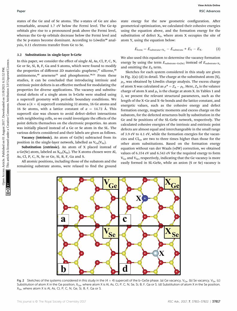
antimonene,49 arsenene31 and phosphorene.50,51 From thesestudies, it can be concluded that introducing intrinsic andextrinsic point defects is an effective method for modulating theproperties for diverse applications. The vacancy and substitu-tional defects of a single atom in b-GeSe were studied usinga supercell geometry with periodic boundary conditions. Wechose a (4 � 4) supercell containing 32 atoms, 16 Ge atoms and16 Se atoms, with a lattice constant of a ¼ 14.72 A. Thissupercell size was chosen to avoid defect–defect interactionswith neighboring cells, so we could investigate the effects of thepoint defects themselves on the electronic properties. An atomwas initially placed instead of a Ge or Se atom in the SL. Thevarious defects considered and their labels are given as follows.
Vacancy (intrinsic). An atom of Ge(Se) subtracted from itsposition in the single-layer network, labelled as VGe(VSe).
Substitution (extrinsic). An atom of X placed instead ofa Ge(Se) atom, labeled as XGe(XSe). The X atoms chosen were Al,As, Cl, P, C, N, Se or Ge, Si, B, F, Ga and S.
All atomic positions, including those of the subatom and theremaining substrate atoms, were relaxed to nd the ground
Fig. 2 Sketches of the systems considered in this study in the (4 � 4) supSubstitution of atom X in the Ge position, XGe, where atom X is Al, As, Cl,XSe, where atom X is Al, As, Cl, P, C, N, Ge, Si, B, F, Ga or S.
This journal is © The Royal Society of Chemistry 2017
state energy for the new geometric conguration. Aergeometrical optimization, we calculated their cohesive energiesusing the equation above, and the formation energy for thesubstitution of defect XY, where atom X occupies the site ofatom Y, using the equation below:
Eform ¼ Esubstrate+XY� Esubstrate + EY � EX. (2)
We also used this equation to determine the vacancy formationenergy by using the term Esubstrate–Ge(Se) instead of Esubstrate+XY
and omitting the EX term.Sketches for each system considered in this study are given
in Fig. 2(a)–(d) in detail. The charge at the substituted atom (X),rL, was obtained by Lowdin charge analysis. The excess chargeof atom X was calculated as r*¼ ZA � rL. Here, ZA is the valancecharge of atom X and rL is the charge at atom X. In Tables 1 and2, we present the relevant structural parameters, such as thelength of the X–Ge and X–Se bonds and the lattice constant, andenergetic values, such as the cohesive energy and defectformation energy, magnetic moments and excess charge on thesubatom, for the defected structures built by substitution in theGe and Se positions of the SL-GeSe network, respectively. Thecalculated cohesive energies of the intrinsic and extrinsic pointdefects are almost equal and interchangeable in the small rangeof 3.9 eV to 4.1 eV, while the formation energies for the vacan-cies and ClGe are two to three times higher than those for theother atom substitutions. Based on the formation energyequation without van der Waals (vdW) correction, we obtainedvalues of 6.354 eV and 6.543 eV for the required energy to formVGe and VSe, respectively, indicating that the Ge vacancy is moreeasily formed in SL-GeSe, while an anion (S or Se) vacancy is
ercell of the b-GeSe phase. (a) Ge vacancy, VGe. (b) Se vacancy, VSe. (c)P, C, N, Se, Si, B, F, Ga or S. (d) Substitution of atom X in the Se position,
RSC Adv., 2017, 7, 37815–37822 | 37817

Table 1 Calculated parameters for atom substitutions in the (4� 4) supercells of GeSe in the Ge position. Ecoh is the cohesive energy; Eform is theformation energy; a is the lattice constant (NC indicates that the lattice constant is not changed), which is the same as in the bare single-layer;d(X–Ge) and d(X–Se) are the bond distances between the substituted (X) and Ge and Se atoms in b-GeSe, respectively (for VGe, the bond distancesare given for Se–Ge and Se–Se); m is the local magneticmoment (NM indicates a nonmagnetic system); r* is the excess charge on the substitutedatom, obtained by subtracting the charge on the substituted atom from its valence charge (a negative sign indicates excess electrons). For VGe,the excess charges on the atoms around the vacancy are given in the table
System Ecoh (eV) Eform (eV) a (A) d(X–Ge) (A) d(X–Se) (A) m (mB) r* (e)
VGe 3.946 6.354 NC 2.50 3.67 2.00 �0.05BGe 4.037 0.895 14.62 3.83 1.99 1.00 �0.37AlGe 3.995 2.170 NC 3.68 2.45 1.00 0.22GaGe 3.965 3.211 NC 3.74 2.51 1.00 0.04CGe 4.053 1.496 14.52 3.52 2.08 NM �0.58SiGe 4.036 0.856 14.67 3.65 2.47 NM 0.10NGe 4.026 1.268 14.58 3.58 2.07 0.48 �0.57PGe 3.998 2.073 NC 3.63 2.39 NM 0.07AsGe 3.985 2.497 NC 3.64 2.54 NM 0.13SGe 3.967 3.127 14.65 3.36 2.26 NM �0.04SeGe 3.949 3.632 NC 3.44 2.40 NM 0.08FGe 3.943 3.903 14.66 3.14 1.84 1.00 �0.41ClGe 3.879 5.934 NC 3.68 3.01 3.00 �0.33
RSC Advances Paper
Ope
n A
cces
s A
rtic
le. P
ublis
hed
on 0
1 A
ugus
t 201
7. D
ownl
oade
d on
11/
8/20
21 6
:31:
52 P
M.
Thi
s ar
ticle
is li
cens
ed u
nder
a C
reat
ive
Com
mon
s A
ttrib
utio
n 3.
0 U
npor
ted
Lic
ence
.View Article Online
more favorable for SL-GaS and -GaSe.52,53 The Ge vacancy doesnot change the supercell lattice constant, while the Se vacancycauses a small structural shrink. Upon Ge vacancy formation,three dangling bonds remain surrounding the vacancy, with0.07 A smaller Ge–Se bond lengths than those in the bare single-layer. Because of these dangling bonds, three unpaired elec-trons exist in the atoms surrounding the vacancy, and they formone bonding and one antibonding orbital. Due to spin-polarization, unoccupied antibonding states occur above theFermi level, as illustrated in Fig. 4. The new system has a localmagnetic moment of 2 mB, in addition to ferromagnetism, andhalf-metallicity occurs upon Ge vacancy formation. In contrastto the Ge vacancy, aer relaxation, the GeSe lattice constant ofthe supercell becomes 0.14 A smaller than that of the bare one.This atomic replacement is called the pseudo Jahn–Teller
Table 2 Calculated parameters for atom substitutions in the (4� 4) supeformation energy; a is the lattice constant (NC indicates that the lattice cd(X–Ge) and d(X–Se) are the bond distances between the substituted (X) anare given for Ge–Ge and Se–Ge); m is the local magnetic moment (Nsubstituted atom, obtained by subtracting the charge on the substitutedtrons). For VSe, the excess charges on the atoms around the vacancy are
System Ecoh (eV) Eform (eV) a (A)
VSe 3.975 6.543 14.58BSe 4.010 1.458 14.65AlSe 3.912 3.284 NCGaSe 3.939 3.743 NCCSe 4.078 0.136 14.62SiSe 4.007 1.519 NCGeSe 3.990 1.927 NCNSe 4.099 1.676 14.60PSe 4.033 0.696 NCAsSe 4.013 1.335 NCSSe 4.043 0.439 14.65FSe 3.996 1.939 14.64ClSe 3.953 3.325 NC
37818 | RSC Adv., 2017, 7, 37815–37822
effect,54 and it induces a nonmagnetic system, whereas thesystem has a magnetic moment before relaxation according toLiebs theorem. Another way to tune the electronic andmagneticproperties of the system is to change the carrier density bycreating impurities in the bare system. For this investigation wechose p-block elements. These atoms can be categorized for theGe(Se) host atom as follows: (1) fewer p electrons than theGe(Se) atom, (2) isovalency with Ge(Se) and (3) more p electronsthan Ge(Se).
We started our investigation on substituted atoms in the Geposition. Aer optimization following substitutional doping,local defects and reconstructions occur in single-layer b-GeSe.Some of the substituted atoms change the lattice constant andcreate new bond lengths around the defects, and these valuesare given in Table 1. The cohesive energies and formation
rcells of GeSe in the Se position. Ecoh is the cohesive energy; Eform is theonstant is not changed), which is the same as in the bare single-layer;d Ge and Se atoms in b-GeSe, respectively (for VSe, the bond distancesM indicates a nonmagnetic system); r* is the excess charge on theatom from its valence charge (a negative sign indicates excess elec-given in the table
d(X–Ge) (A) d(X–Se) (A) m (mB) r* (e)
2.94 2.59 NM 0.082.10 3.66 1.00 �0.362.59 3.84 1.00 0.282.60 3.86 1.00 0.092.03 3.66 NM �0.462.45 3.77 NM 0.192.52 3.79 NM 0.142.02 3.66 1.00 �0.582.42 3.70 1.00 �0.032.52 3.72 1.00 0.042.45 3.64 NM �0.152.37 3.61 1.00 �0.442.49 3.56 1.00 �0.16
This journal is © The Royal Society of Chemistry 2017

Fig. 3 Cohesive energy, defect formation energy and magneticmoments for the vacancy systems (VGe and VSe) and X atomsubstituted systems (X¼ Al, As, Cl, P, C, N, Se or Ge, Si, B, F, Ga and S) inthe Ge position and Se position in the (4 � 4) supercell of the b-GeSephase.
Paper RSC Advances
Ope
n A
cces
s A
rtic
le. P
ublis
hed
on 0
1 A
ugus
t 201
7. D
ownl
oade
d on
11/
8/20
21 6
:31:
52 P
M.
Thi
s ar
ticle
is li
cens
ed u
nder
a C
reat
ive
Com
mon
s A
ttrib
utio
n 3.
0 U
npor
ted
Lic
ence
.View Article Online
energies for all of the considered systems are given in Fig. 3. Asevident in Fig. 3 and Table 1, the cohesive energies decreasewith an increase in period for the same group number, while theformation energies increase. These results are as expected, aswith an increasing atomic radius and decreasing electronega-tivity of the dopant atoms, the doping feasibility becomesharder with the increasing period, and binding will be weakerand the cohesive energy will decrease. In accordance with theseresults, the formation energies of defects with atoms B, C, N andSi in the Ge position in the network are lower than those of theother atoms and vacancies. These differences can indicate that
This journal is © The Royal Society of Chemistry 2017
these point defects may be more dominant defects during thefabrication of single-layer b-GeSe. To investigate the change inthe electronic structure of the new systems, we calculated theirelectronic partial density of states (PDOS) and their bandstructures, as illustrated in Fig. 4 and 5. According to ourextensive calculations, the substitution of group IIIA atoms onGe sites yields a magnetic semiconductor material (m¼ 1 mB), asseen in Fig. 4 and 5. By increasing the atomic radius, impuritystates in the spin-up channel slip below the Fermi level, andalso the conduction bands move to the upper energy levels. Asseen in the gures, the impurity states are composed of the p-orbitals of the dopants (B, Al, Ga, etc.) and the p-orbitals ofthe Se atoms, which are around the defects. All group IIIAdopant systems show n-type semiconductor properties for thespin-down channels, therefore charge transfer becomes easierthan in the bare GeSe state. When C or Si are substituted on a Gesite, as seen in Table 1, the cohesive energies of the system areclosest to the cohesive energy of bare GeSe, because they havethe same number of valence electrons. If we compare the totaldensity of states of GeSe with that of CGe and SiGe, we can seesimilarities in the general trends of the DOS, and also theirband structures are the same except for the impurity states.Again, with an increase in the atomic radius, the impurity statesgo to deeper energy levels. Although the atomic radii arechanging, the nonmagnetic semiconductor properties areconserved because C and Si possess the same number of valenceelectrons as the Ge atom. For example, when the dopants havethree more electrons from the host Ge atom, such as in groupVIIA, the system attains a magnetic moment and GeSe becomesa magnetic semiconductor. As seen in the FGe part of Fig. 5,there is one shallow state in both of the spin-up and downstates, which lies near the conduction band minimum (CBM).For FGe and ClGe, there are donor bands instead of donor statesin the spin-up states in the vicinity of the Fermi level. If the rstBohr radius is large, these kinds of band occur due to the donororbital overlapping, even though the doping ratio is low.Different to the other mentioned dopants, GeSe can showmetallic behavior with a doped atom in the Ge position whichhas one more valence electron than the Ge atom, such as atomsfrom group VA. By substituting N, P or As atoms into a Ge site,impurity bands occur in the Fermi level due to the p-orbitals ofthe dopants and Se atoms around the defect. In addition, Ndoping on a Ge site raises the magnetic moment of the systemby 0.5 mB.
We also investigated the substitution of the same atoms inthe Se position. As seen in Fig. 3, similar trends for theformation (cohesive) energy values are valid for the XSe struc-tures. Their values increase (decrease) with an increasingperiod. The most dominant defect is the CSe defect, and thesubstitution of an S atom instead of a Se atom is anotherfavorable defect type with a lower formation energy. Similar tothe XGe defect, some of the XSe structures have smaller latticeconstants than that of the bare GeSe structure. We did notencounter a structure that was larger than bare GeSe. Thissituation can be attributed to our selection of dopant atoms,which are all light elements. We suppose that the GeSestructure will be enlarged with heavy elements. Similar to XGe,
RSC Adv., 2017, 7, 37815–37822 | 37819

Fig. 4 Total (shown by black lines), subatom and atoms around the defect projected density of states for a single atom, substituted in the Geposition, in the (4 � 4) supercell of the b-GeSe phase. Zero energy is set to the Fermi level, EF, shown by dashed dotted lines.
RSC Advances Paper
Ope
n A
cces
s A
rtic
le. P
ublis
hed
on 0
1 A
ugus
t 201
7. D
ownl
oade
d on
11/
8/20
21 6
:31:
52 P
M.
Thi
s ar
ticle
is li
cens
ed u
nder
a C
reat
ive
Com
mon
s A
ttrib
utio
n 3.
0 U
npor
ted
Lic
ence
.View Article Online
substituted atoms in the Se position change the electronicstructure and cause localized states in the fundamental bandgap or resonance states in the band continua of b-GeSe.However, different to XGe, there are many half metallicsystems for the XSe defect type. Group IIIA doping gives rise to
Fig. 5 Total (shown by black lines), subatom and atoms around thedefect projected density of states for a single atom, substituted in theGe position, in the (4 � 4) supercell of the b-GeSe phase. Bandstructures are also illustrated in the vicinity of the Fermi level. Zeroenergy is set to the Fermi level, EF, shown by dashed dotted lines.
37820 | RSC Adv., 2017, 7, 37815–37822
localized states in the fundamental band gap of GeSe. B, Aland Ga doping yields similar band structures with differentband gap values, so we only give the GaSe band structure (seeFig. 6). As seen in Fig. 7, there are half-occupied acceptorbands in the Fermi level, and one unoccupied acceptor statenear the VBM for the spin-up channel. These acceptor bandsand state become nearly 0.1 eV lower in energy, and the systemshows semiconductor properties for the spin-down channel.C, Si or Ge doping in the Se position gives similar electronicstructures to each other, and the new systems display p-typenonmagnetic semiconductor properties due to the shallowstates near the CBM. When we substituted group VA atoms inthe Se position, we attained magnetic (m ¼ 1 mB) semi-conductor materials resulting from the one extra hole in thecrystals. PDOS are given in Fig. 6, and we also plot the bandstructure of PSe and illustrate it in Fig. 7. NSe and AsSe also havesimilar bands. As is evident in Fig. 7, there is one occupied andunoccupied impurity state in the spin-up and spin-downchannels, respectively. All group VA doped systems are p-type semiconductors for the spin-down state. Replacing Sewith S atoms almost does not change the electronic structureof GeSe, and only the degeneracy decreases due to a very smallstructural shrink. If we add dopants which have one moreelectron than Se, such as F and Cl, the systems have a 1 mB
magnetic moment and show half-metallicity properties for Fdoping, while remaining a semiconductor for Cl doping.
This journal is © The Royal Society of Chemistry 2017

Fig. 7 Total (shown by black lines), subatom and atoms around thedefect projected density of states for a single atom, substituted in theSe position, in the (4 � 4) supercell of the b-GeSe phase. Bandstructures are also illustrated in the vicinity of the Fermi level. Zeroenergy is set to the Fermi level, EF, shown by dashed dotted lines.
Fig. 6 Total (shown by black lines), subatom and atoms around thedefect projected density of states for a single atom, substituted in theSe position, in the (4� 4) supercell of the b-GeSe phase. Zero energy isset to the Fermi level, EF, shown by dashed dotted lines.
Paper RSC Advances
Ope
n A
cces
s A
rtic
le. P
ublis
hed
on 0
1 A
ugus
t 201
7. D
ownl
oade
d on
11/
8/20
21 6
:31:
52 P
M.
Thi
s ar
ticle
is li
cens
ed u
nder
a C
reat
ive
Com
mon
s A
ttrib
utio
n 3.
0 U
npor
ted
Lic
ence
.View Article Online
4 Conclusions
In conclusion, we present a theoretical study on the effects ofpoint defects in single-layer b-GeSe, systematically studied bymeans of rst principles plane-wave calculations within densityfunctional theory. On the basis of the DFT results, bare SL-GeSeis a stable buckled honeycomb structure with semiconductingbehavior and is nonmagnetic. Our calculations show thata magnetism of 2 mB can be induced by a single Ge vacancy inthe b-GeSe phase, but a Se vacancy does not induce any
This journal is © The Royal Society of Chemistry 2017
magnetization in the system. Aer the substitution process,some of the atoms give rise to magnetic states, so b-GeSe canattain magnetism and can have a half-metallic, metallic orsemiconductor character. The calculated cohesive energiesrange from 3.9 eV to 4.1 eV, which shows that all of theconsidered dopants can strongly interact with SL-GeSe. Ourresults show that the group number is the most importantfactor to determine the magnetic and electronic structure ofdoped GeSe. If we doped b-GeSe with atoms which have oddnumbers of valence electrons, the doped GeSe would attaina magnetic moment resulting from the remaining one unpairedelectron or hole in the crystal. If we doped b-GeSe with evenvalence number dopants, the doped GeSe would remaina semiconductor, but would show a p- or n-type character. Webelieve that these results are useful for the further functionali-zation of b-GeSe with point defects.
References
1 K. S. Novoselov, Science, 2004, 306, 666–669.2 K. S. Novoselov, A. K. Geim, S. V. Morozov, D. Jiang,M. I. Katsnelson, I. V. Grigorieva, S. V. Dubonos andA. A. Firsov, Nature, 2005, 438, 197–200.
3 A. A. Balandin, S. Ghosh, W. Bao, I. Calizo, D. Teweldebrhan,F. Miao and C. N. Lau, Nano Lett., 2008, 8, 902–907.
4 S. Ghosh, I. Calizo, D. Teweldebrhan, E. P. Pokatilov,D. L. Nika, A. A. Balandin, W. Bao, F. Miao and C. N. Lau,Appl. Phys. Lett., 2008, 92, 151911.
5 Y. Zhang, Y.-W. Tan, H. L. Stormer and P. Kim, Nature, 2005,438, 201–204.
6 E. Durgun, S. Tongay and S. Ciraci, Phys. Rev. B: Condens.Matter Mater. Phys., 2005, 72, 075420.
7 S. Cahangirov, M. Topsakal, E. Akturk, H. Sahin andS. Ciraci, Phys. Rev. Lett., 2009, 102, 236804.
8 P. Vogt, P. De Padova, C. Quaresima, J. Avila,E. Frantzeskakis, M. C. Asensio, A. Resta, B. Ealet andG. Le Lay, Phys. Rev. Lett., 2012, 108, 155501.
9 V. O. Ozçelik, E. Durgun and S. Ciraci, J. Phys. Chem. Lett.,2014, 5, 2694–2699.
10 Y. Xu, B. Yan, H.-J. Zhang, J. Wang, G. Xu, P. Tang, W. Duanand S.-C. Zhang, Phys. Rev. Lett., 2013, 111, 136804.
11 H. Sahin, S. Cahangirov, M. Topsakal, E. Bekaroglu,E. Akturk, R. T. Senger and S. Ciraci, Phys. Rev. B: Condens.Matter Mater. Phys., 2009, 80, 155453.
12 M. Topsakal, S. Cahangirov, E. Bekaroglu and S. Ciraci, Phys.Rev. B: Condens. Matter Mater. Phys., 2009, 80, 235119.
13 J. N. Coleman, M. Lotya, A. O’Neill, S. D. Bergin, P. J. King,U. Khan, K. Young, A. Gaucher, S. De and R. J. E. A. Smith,Science, 2011, 331, 568–571.
14 C. Ataca, H. Sahin and S. Ciraci, J. Phys. Chem. C, 2012, 116,8983–8999.
15 V. O. Ozçelik, O. U. Akturk, E. Durgun and S. Ciraci, Phys.Rev. B: Condens. Matter Mater. Phys., 2015, 92, 125420.
16 Z. Zhu and D. Tomanek, Phys. Rev. Lett., 2014, 112, 176802.17 Y. Aierken, D. Çakir, C. Sevik and F. M. Peeters, Phys. Rev. B:
Condens. Matter Mater. Phys., 2015, 92, 081408.
RSC Adv., 2017, 7, 37815–37822 | 37821

RSC Advances Paper
Ope
n A
cces
s A
rtic
le. P
ublis
hed
on 0
1 A
ugus
t 201
7. D
ownl
oade
d on
11/
8/20
21 6
:31:
52 P
M.
Thi
s ar
ticle
is li
cens
ed u
nder
a C
reat
ive
Com
mon
s A
ttrib
utio
n 3.
0 U
npor
ted
Lic
ence
.View Article Online
18 D. Çakir, C. Sevik and F. M. Peeters, Phys. Rev. B: Condens.Matter Mater. Phys., 2015, 92, 165406.
19 C. Kamal and M. Ezawa, Phys. Rev. B: Condens. Matter Mater.Phys., 2015, 91, 085423.
20 D. Kecik, E. Durgun and S. Ciraci, Phys. Rev. B: Condens.Matter Mater. Phys., 2016, 94, 205409.
21 D. Kecik, E. Durgun and S. Ciraci, Phys.Rev. B: Condens.Matter Mater. Phys., 2016, 94, 205410.
22 O. U. Akturk, V. O. Ozҫelik and S. Ciraci, Phys. Rev. B:Condens. Matter Mater. Phys., 2015, 91, 235446.
23 E. Akturk, O. U. Akturk and S. Ciraci, Phys. Rev. B: Condens.Matter Mater. Phys., 2016, 94, 014115.
24 S. Zhang, Z. Yan, Y. Li, Z. Chen and H. Zeng, Angew. Chem.,Int. Ed., 2015, 54, 3112–3115.
25 B. Mukherjee, Y. Cai, H. R. Tan, Y. P. Feng, E. S. Tok andC. H. Sow, ACS Appl. Mater. Interfaces, 2013, 5, 9594–9604.
26 C. Lan, C. Li, Y. Yin, H. Guo and S. Wang, J. Mater. Chem. C,2015, 3, 8074–8079.
27 Y. Hu, S. Zhang, S. Sun, M. Xie, B. Cai and H. Zeng, Appl.Phys. Lett., 2015, 107, 122107.
28 F. O. von Rohr, H. Ji, F. A. Cevallos, T. Gao, N. P. Ong andR. J. Cava, J. Am. Chem. Soc., 2017, 139, 2771–2777.
29 H. Arkin and E. Akturk, Appl. Surf. Sci., 2016, 390, 185–189.30 C. Ataca and S. Ciraci, J. Phys. Chem. C, 2011, 115, 13303–
13311.31 F. Ersan, E. Akturk and S. Ciraci, J. Phys. Chem. C, 2016, 120,
14345–14355.32 E. Bekaroglu, M. Topsakal, S. Cahangirov and S. Ciraci, Phys.
Rev. B: Condens. Matter Mater. Phys., 2010, 81, 075433.33 B. Xu, J. Yin, Y. D. Xia, X. G. Wan and Z. G. Liu, Appl. Phys.
Lett., 2010, 96, 143111.34 A. Gokҫe and E. Akturk, Appl. Surf. Sci., 2015, 332, 147–151.35 M.-Y. Liu, Y. Huang, Q.-Y. Chen, C. Cao and Y. He, Sci. Rep.,
2016, 6, 29114.36 F. Ersan, A. G. Gokҫe and E. Akturk, Appl. Surf. Sci., 2016,
389, 1–6.
37822 | RSC Adv., 2017, 7, 37815–37822
37 F. Ersan, G. Gokoglu and E. Akturk, J. Phys.: Condens. Matter,2014, 26, 325303.
38 Y. Ding and Y. Wang, Phys. Chem. Chem. Phys., 2016, 18,23080–23088.
39 P. E. Blochl, Phys. Rev. B: Condens. Matter Mater. Phys., 1994,50, 17953.
40 J. P. Perdew, K. Burke and M. Ernzerhof, Phys. Rev. Lett.,1996, 77, 3865.
41 P. Giannozzi, S. Baroni, N. Bonini, M. Calandra, R. Car,C. Cavazzoni, D. Ceresoli, G. L. Chiarotti, M. Cococcioniand I. E. A. Dabo, J. Phys.: Condens. Matter, 2009, 21, 395502.
42 H. J. Monkhorst and J. D. Pack, Phys. Rev. B: Condens. MatterMater. Phys., 1976, 13, 5188–5192.
43 C. G. Broyden, IMA J. Appl. Math., 1970, 6, 76–90.44 A. V. Krukau, O. A. Vydrov, A. F. Izmaylov and G. E. Scuseria,
J. Chem. Phys., 2006, 125, 224106.45 C. Hartwigsen, S. Goedecker and J. Hutter, Phys. Rev. B:
Condens. Matter Mater. Phys., 1998, 58, 3641–3662.46 P.-O. Lowdin, J. Chem. Phys., 1950, 18, 365–375.47 K. T. Chan, J. B. Neaton and M. L. Cohen, Phys. Rev. B:
Condens. Matter Mater. Phys., 2008, 77, 235430.48 X. Lin and J. Ni, Phys. Rev. B: Condens. Matter Mater. Phys.,
2012, 86, 075440.49 O. Uzengi Akturk, E. Akturk and S. Ciraci, Phys. Rev. B:
Condens. Matter Mater. Phys., 2016, 93, 035450.50 G. Wang, R. Pandey and S. P. Karna, Appl. Phys. Lett., 2015,
106, 173104.51 H. Zheng, H. Yang, H. Wang, X. Du and Y. Yan, J. Magn.
Magn. Mater., 2016, 408, 121–126.52 L. Ao, H. Y. Xiao, X. Xiang, S. Li, K. Z. Liu, H. Huang and
X. T. Zu, Phys. Chem. Chem. Phys., 2015, 17, 10737–10748.53 T. Cao, Z. Li and S. G. Louie, Phys. Rev. Lett., 2015, 114,
236602.54 B. Bersuker, J. Phys.: Conf. Ser., 2017, 833, 012001.
This journal is © The Royal Society of Chemistry 2017