Embed Size (px)
Citation preview

The anatomy of the Gunn laserS. Chung and N. Balkan Citation: J. Appl. Phys. 104, 073101 (2008); doi: 10.1063/1.2977719 View online: http://dx.doi.org/10.1063/1.2977719 View Table of Contents: http://jap.aip.org/resource/1/JAPIAU/v104/i7 Published by the American Institute of Physics. Related ArticlesHigh beta lasing in micropillar cavities with adiabatic layer design Appl. Phys. Lett. 102, 052114 (2013) Portable optical-resolution photoacoustic microscopy with a pulsed laser diode excitation Appl. Phys. Lett. 102, 053704 (2013) Electro-optical and lasing properties of hybrid quantum dot/quantum well material system for reconfigurablephotonic devices Appl. Phys. Lett. 102, 053110 (2013) Laser emissions from one-dimensional photonic crystal rings on silicon-dioxide Appl. Phys. Lett. 102, 051103 (2013) High-brightness tapered quantum cascade lasers Appl. Phys. Lett. 102, 053503 (2013) Additional information on J. Appl. Phys.Journal Homepage: http://jap.aip.org/ Journal Information: http://jap.aip.org/about/about_the_journal Top downloads: http://jap.aip.org/features/most_downloaded Information for Authors: http://jap.aip.org/authors
Downloaded 11 Feb 2013 to 155.245.46.3. Redistribution subject to AIP license or copyright; see http://jap.aip.org/about/rights_and_permissions

The anatomy of the Gunn laserS. Chung1 and N. Balkan2,a�
1Department of Nano-Optics, Korea Polytechnic University, 2121 Jeongwang-dong, Shiheung City,Gyeonggi-do 429-793, Republic of Korea2Department of Computing and Electronic Systems Engineering, University of Essex, Colchester CO4 3SQ,United Kingdom
�Received 14 April 2008; accepted 11 July 2008; published online 1 October 2008�
A monopolar GaAs Fabry–Pérot cavity laser based on the Gunn effect is studied bothexperimentally and theoretically. The light emission occurs via the band-to-band recombination ofimpact-ionized excess carriers in the propagating space-charge �Gunn� domains.Electroluminescence spectrum from the cleaved end-facet emission of devices withGa1−xAlxAs �x=0.32� waveguides shows clearly a preferential mode at a wavelength around 840nm at T=95 K. The threshold laser gain is assessed by using an impact ionization coefficientresulting from excess carriers inside the high-field domain. © 2008 American Institute of Physics.�DOI: 10.1063/1.2977719�
I. INTRODUCTION
We have shown recently that light is emitted from activeregion of a GaAs Gunn diode due to band-to-band recombi-nation of impact-ionized carriers created by the high electricfield in the propagating space-charge domains.1 We also re-ported the correlation between the spontaneous emission in-tensity and the device length2 and predicted that the sponta-neous emission may evolve into stimulated emission when itis placed in a Fabry–Pérot �FP� cavity.3
In this paper we present our results of the currentdensity–electric field �J-F� and electroluminescence �EL�intensity–electric field �L-F� characteristics together with theEL spectra of stimulated emission from the Gunn device. Wealso present the theoretical analysis and Monte Carlo simu-lation of the light emission mechanism invoking a combina-tion of well-established physical phenomena, including thedrift velocity saturation, impact ionization, and populationinversion in GaAs.
II. EXPERIMENTAL
The waveguided sample used in the studies had a n-typeGaAs active layer sandwiched betweenAlxGa1−xAs /GaAs �x=0.32� wave-guiding layers. TheGaAs active layer had a carrier concentration of n=4.8�1017 cm−3 and a layer thickness of 1 �m. The wave-guiding layers and device structure together with contactconfiguration are shown in Figs. 1�a� and 1�b�. The modifieddumb-bell pattern shown in Fig. 1�b� was developed duringour studies to provide emission facets without the introduc-tion of loss regions that may occur as a result of contactdiffusion in a conventional two terminal device.
Voltage pulses of duration ranging between 85 and 105ns with a duty cycle less than 0.015% were applied along thedevice. The applied electric field was deduced from the volt-age drop, taking into account aspect ratio of active region asdescribed in Sec. III, between electrodes of the sample di-
vided by its length. The current flow through the device wasdetermined by measuring the voltage across a 50 � resistorplaced in series with the device. The light emitted from thesample was collected by an antireflective lens and dispersedusing a 1/3 m monochromator �Bentham, M 300EA, 830grooves/mm� which was fitted with bilateral straight slits, thewidth of which was variable between 10 �m and 8 mm. Thespectra were detected using a cooled GaAs photomultiplier�Hamamatsu, R1767�. The data were averaged and capturedusing a digital oscilloscope �Tektronix, TDS2012� with abandwidth of 100 MHz.
III. RESULTS
In order to determine correctly the threshold field fornegative differential resistance �NDR� aspect ratio of the ac-
a�Electronic addresses: [email protected] and [email protected].
(a)
(b)
FIG. 1. �Color online� Wafer structure and device geometry of Gunn-effectlaser; �a� waveguided structure and �b� FP device. The in-plane and verticalarrows in �a� indicate end-edge emission and top-surface emission,respectively.
JOURNAL OF APPLIED PHYSICS 104, 073101 �2008�
0021-8979/2008/104�7�/073101/9/$23.00 © 2008 American Institute of Physics104, 073101-1
Downloaded 11 Feb 2013 to 155.245.46.3. Redistribution subject to AIP license or copyright; see http://jap.aip.org/about/rights_and_permissions
tive region w /L should be taken into account. This is becausethe electric field calculated from the voltage drop along theactive layer may be different from the true value for largeaspect ratios. Assuming the uniform electric field along theconduction channel, the general expression for resistance isgiven by4
R =L
���S=
L
���wt=
1
���rt, �1�
where the cross-sectional area of active layer is S=w� t withthe width w and the thickness t. � is the medium conductiv-ity and r is the aspect ratio of active area defined by r=w /L.
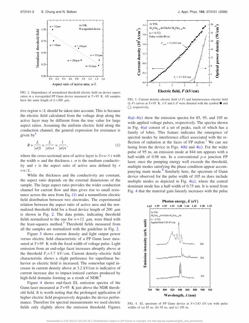
While the thickness and the conductivity are constant,the aspect ratio depends on the external dimensions of thesample. The large aspect ratio provides the wider conductionchannel for current flow and thus gives rise to small resis-tance across the area from Eq. �1� and a nonuniform electricfield distribution between two electrodes. The experimentalrelation between the aspect ratio of active area and the nor-malized threshold field for a fixed device length of 200 �mis shown in Fig. 2. The data points, indicating thresholdfields normalized to the one for w=12 �m, were fitted withthe least-squares method.5 Threshold fields measured fromall the samples are normalized with the guideline in Fig. 2.
Figure 3 shows current density and light output powerversus electric field characteristic of a FP Gunn laser mea-sured at T=95 K with the fixed width of voltage pulse. Lightemission from an end-edge facet increases abruptly above atthe threshold Fi=3.7 kV /cm. Current density–electric fieldcharacteristic shows a slight preference for superlinear be-havior as electric field is increased. The somewhat rapid in-crease in current density above at 3.2 kV/cm is indicative ofcurrent increase due to impact-ionized carriers produced byhigh-field domains forming as a result of NDR.6
Figure 4 shows end-facet EL emission spectra of theGunn laser measured at T=95 K just above the NDR thresh-old field. It is worth noting that the prolonged application ofhigher electric field progressively degrades the device perfor-mance. Therefore for spectral measurements we used electricfields only slightly above the emission threshold. Figures
4�a�–4�c� show the emission spectra for 85, 95, and 105 nswide applied voltage pulses, respectively. The spectra shownin Fig. 4�a� consist of a set of peaks, each of which has afamily of lobes. This feature indicates the emergence ofspectral modes by interference effect associated with the re-flection of radiation at the faces of FP etalon.7 We can seelasing from the device in Figs. 4�b� and 4�c�. For the widerpulse of 95 ns, an emission mode at 844 nm appears with ahalf-width of 0.98 nm. In a conventional p-n junction FPlaser, once the pumping energy well exceeds the threshold,multiple modes satisfying the phase condition appear accom-panying main mode.8 Similarly here, the spectrum of Gunndevice observed for the pulse width of 105 ns does includemultiple modes as depicted in Fig. 4�c�, where the centraldominant mode has a half-width of 0.75 nm. It is noted fromFig. 4 that the material gain linearly increases with the pulse
FIG. 2. Dependence of normalized threshold electric field on device aspectratios in a waveguided FP Gunn device measured at T=95 K. All sampleshave the same length of L=200 �m. FIG. 3. Current density–electric field �J-F� and luminescence–electric field
�L-F� curves at T=95 K. J-F and L-F were denoted with the symbol � and�, respectively.
FIG. 4. EL spectrum of FP Gunn device at F=3.83 kV /cm with pulsewidths of �a� 85 ns, �b� 95 ns, and �c� 105 ns.
073101-2 S. Chung and N. Balkan J. Appl. Phys. 104, 073101 �2008�
Downloaded 11 Feb 2013 to 155.245.46.3. Redistribution subject to AIP license or copyright; see http://jap.aip.org/about/rights_and_permissions

width at the fixed voltage, indicative of the good controlla-bility of the pulse width on gain relating to light emission. Itis because the impact-ionized excess carrier density in aGunn device is proportional to the transit number of the do-main, which, in turn, is defined by the voltage pulse width.Hence the impact-ionized carrier density and the correspond-ing gain can be effectively controlled by a pulse width. Incontrast, the applied field gives rise to the significant in-creases in the gain even with small amount over a NDRthreshold. This might lead rightly to device degradation. Thedisadvantage of electric field operation is due to surgical cur-rent increase by considerable impact ionization made bymultiple domains. Once the carrier multiplication processstarts the current increases rapidly and the control over thedevice is lost leading to the destruction of the device due toexcessive Joule heating.
IV. THEORETICAL MODEL
A. Electron transport model by Monte Carlotechnique „Ref. 9…
In order to determine theoretically the onset of lightemission, hence the NDR threshold, electron transport char-acteristics at high electric fields in GaAs were investigatedusing a Monte Carlo technique that took into account of theionized-impurity and phonon scatterings in the parabolic �and L valleys.1 The phonon scattering mechanisms permittedin the simulation are acoustic, optical, equivalent intervalley�EI�, and nonequivalent intervalley �NEI�. Simulation pro-cesses are described as follows.
Range and parameters. The simulation is accomplished
in the range of electric fields between 0 and 10 kV/cm. Theproper convergence of data is achieved by giving 2000 as thenumber of a real scattering events and using 100 V/cm as anelectric field interval. Phonon energies and phonon occupa-tion ratios for optical, EI, and NEI scattering are deducedfrom the respective phonon frequencies given in Table I.
Calculation. In a central valley, the rates of each scatter-ing event can be estimated by using the proper equationsgiven by Casey and Panish.8 All the phonon scattering ratesare calculated with the meshed energies �E� involving pho-non energy changes, i.e., E+�� for phonon absorption andE−�� for phonon emission. Ionized impurity scattering doesnot invoke an energy loss since it is an elastic scattering.Hence the given meshed energy E is taken into account forthe scattering.
Initialization. It is assumed that an electron drift alongthe kz axis in the �k� ,kz� coordinate k space, where k� repre-sents the sum of kx and ky vectors, remains fixed during anelectron flight. The simulation is commenced with an arbi-trary initial electron energy and position in k space. The ar-bitrary position does not have an influence on the final elec-tron position if a number of drift events are occurredsubsequently.
Selection process. The drift of an electron is terminatedby a “scattering channel selection” process. The scatteringchannel selection is carried out by comparing a number gen-erated randomly by the program with the normalized scatter-ing rates. The comparison procedures are made with intra-valley and, then, intervalley scatterings in order. The rate ofthe first intravalley scattering, i.e., ionized-impurity scatter-ing, 1 is produced by being normalized with the total scat-
TABLE I. Bulk GaAs material parameters used int he calculations.
Parameter Value Unit
Density, �a 5.3176 g /cm3
Velocity of sound, sb 5.24�105 cm/sHigh frequency dielectric constant at T=300 K and95 Kc
10.8862/10.6906 –
�=10.6�1+9�10−5T�Static dielectric constant, at T=300 K and 95 Kc 12.8464/12.5414 –�=12.4�1+1.2�10−4T�Polar optical phonon frequency, �0
c 5.211�1013 rad·s−1
Equivalent intervally phonon frequency, �ec 4.4058�1013 rad·s−1
Non-equivalent intervally phonon frequency, ��c 4.2235�1013 rad·s−1
Acoustic deformation potential in central � valley, Dacc 7 eV
Acoustic deformation potential in satellite L valley, Dasc 9.2 eV
Equivalent intervalley coupling constant, De,L-Ld 10 eV/cm
Non-equivalent intervalley coupling constant, Dn,�-Ld 10 eV/cm
Central valley effective mass,mc
� �m0=9.1095�10−31 kg�e0.067m0 kg
Satellite valley effective mass, ms� �m0=9.1095
�10−31 kg�e0.35m0 kg
Number of equivalent L�111� valleysf 4 –
aO. Madelung, Semiconductors-Basic Data, 2nd ed. �Springer, Berlin, 1996�, p. 104.bO. Madelung, Semiconductors-Basic Data, 2nd ed. �Springer, Berlin, 1996�, p. 108.cM. A. Littlejohn, J. R. Hauser, and T. H. Glisson, 48�11�, p. 4587 �1977�.dS. Adachi, GaAs and Related Materias: Bulk Semiconducting and Superlattice Properties �World Scientific,Singapore, 19940.eA. D. Boardman, Physics Program �John Wiley & Sons, Chichester, 1980�, p. 355–410.fS. M. Sze, Physics and Semiconductor Devices �John Wiley & Sons, New York, 1981�, p. 647.
073101-3 S. Chung and N. Balkan J. Appl. Phys. 104, 073101 �2008�
Downloaded 11 Feb 2013 to 155.245.46.3. Redistribution subject to AIP license or copyright; see http://jap.aip.org/about/rights_and_permissions
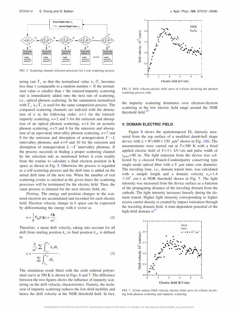
tering rate �s so that the normalized value 1 /�s becomesless than 1 comparable to a random number r. If the normal-ized value is smaller than r the ionized-impurity scatteringrate is immediately added onto the next rate of scattering,i.e., optical phonon scattering. In the summation normalizedwith �s, 2 /�s is used for the same comparison process. Thecompared scattering channels are indexed with the denota-tion of n as the following order: n=1 for the ionized-impurity scattering, n=2 and 3 for the emission and absorp-tion of an optical phonon scattering, n=4 for an acousticphonon scattering, n=5 and 6 for the emission and absorp-tion of an equivalent intervalley phonon scattering, n=7 and8 for the emission and absorption of nonequivalent �→Lintervalley phonons, and n=9 and 10 for the emission andabsorption of nonequivalent L→� intervalley phonons. Ifthe process succeeds in finding a proper scattering channelby the selection rule as mentioned before it exits readilyfrom the routine to calculate a final electron position in kspace as shown in Fig. 5. Otherwise the process is regardedas a self-scattering process and the drift time is added on theinitial drift time of the next run. When the number of realscattering events is satisfied at the given times the scatteringprocesses will be terminated for the electric field. Then, thesame process is initiated for the next electric field, etc.
Plotting. The energy and position changes in the scat-tered electron are accumulated and recorded for each electricfield. Electron velocity change in k space can be expressedby differentiating the energy with k vector as
v =1
��kE�k� =
�k
m�. �2�
Therefore, a mean drift velocity, taking into account for alldrift from starting position kzi to final position kzf, is definedas
v =
�
m� ��kzi
kzf
kzdkz
��kzi
kzf
dkz
. �3�
The simulation result fitted with the sixth ordered polyno-mial curve at 300 K is shown in Figs. 6 and 7. The differencebetween the two figures shows the influence of impurity scat-tering on the drift velocity characteristics. Namely, the inclu-sion of impurity scattering reduces the low-field mobility andhence the drift velocity at the NDR threshold field. In fact,
the impurity scattering dominates over electron-electronscattering at the low electric field range around the NDRthreshold field.10
V. DOMAIN ELECTRIC FIELD
Figure 8 shows the spatiotemporal EL intensity mea-sured from the top surface of a modified dumb-bell shapedevice with L�W=600�150 �m2 shown in Fig. 1�b�. Themeasurements were carried out at T=300 K with a fixedapplied electric field of F=3.1 kV /cm and pulse width oftpulse=80 ns. The light emission from the device was col-lected by a cleaved Franck-Condon/parity conserving typesingle mode optical fiber with a 9 �m inner core diameter.The traveling time, i.e., domain transit time, was calculatedwith a sample length and a domain velocity vd=1.4�107 cm /s at NDR threshold shown in Fig. 7. The lightintensity was measured from the device surface as a functionof the propagating distance of the traveling domain from thecathode. The light intensity increases linearly during the do-main transit. Higher light intensity corresponding to higherexcess carrier density is created by impact ionization throughthe traveling domain field. A time-dependent potential of thehigh-field domain is11
FIG. 5. Scattering channel selection processes for a real scattering process.
FIG. 6. Drift velocity-electric field curve of n-GaAs involving the phononscattering process only.
FIG. 7. �Color online� Drift velocity–electric field curve of n-GaAs involv-ing both phonon scattering and impurity scattering.
073101-4 S. Chung and N. Balkan J. Appl. Phys. 104, 073101 �2008�
Downloaded 11 Feb 2013 to 155.245.46.3. Redistribution subject to AIP license or copyright; see http://jap.aip.org/about/rights_and_permissions

dVD
dt� �
FR
Fd
�v�FR� − v�F��dF , �4�
where VD is the domain potential. For the steady state,dVD /dt=0 and Eq. �4� satisfies the “equal areas rule,”12
where two closed regions made by electron drift velocity-applied field �solid line� and domain drift velocity-domainfield �dashed-dotted line� curves are equal in Fig. 9�a�. Whenthe current due to the applied field is increased from zero tothe NDR threshold, the high-field domain is nucleated andcontinues to grow at an ever-increasing rate because electronvelocity outside the domain v�FR� does not decrease owingto the constant current injection while domain velocity v�Fd�is retarded by randomly distributed local imperfection in thesemiconductor. It results in the change in time-dependentdomain potential, i.e., dVD /dt�0 in Eq. �4�. Therefore whenelectric fields above the NDR threshold are applied to theGunn device, a propagating domain across the device willgrow in the domain field as shown in Fig. 8 and the equalareas rule is not valid anymore because of the area inequalitybetween two regions. We use Eq. �4� to define the “unequalareas rule.” The electric field in the depletion region �deple-tion field� is13
Fdep =en0x
, �5�
where Fdep is the depletion field. With the assumption ofquite a small diffusion coefficient, the accumulation layerhas a finite thickness and electric field inside, Facc. Maximumdomain electric field satisfies Fdep=Facc at the interface be-tween the accumulation layer and the depletion region.Therefore the relation is given by
enaccdacc
=
en0ddep
, �6�
where ddep and dacc are the thicknesses of depletion regionand accumulation layer, respectively. nacc is the electron den-sity in the accumulation layer. Integration over the thicknessincluding accumulation and depletion region produces do-main potential difference Vd as
Vd =en0ddep
2
2, �7�
where the thickness of the accumulation layer dacc is negli-gible compared to that of the depletion region ddep, and thus,
FIG. 8. �Color online� Spatiotemporal dynamics of a Gunn device withlongitudinal length of 600 �m. The solid and dot lines indicate the bestlinear fit for the data from 0 to 430 �m �marked by a bold arrow� and theguideline for those from 430 to 600 �m, respectively.
FIG. 9. Electric-field-dependent domain field curves drawn by �a� equalareas rule and �b� unequal areas rule at T=95 K. The solid and dashed-dotted lines of �a� indicates a drift velocity–electric field outside the domainproduced by Monte Carlo technique and a drift velocity–electric field insidethe domain, respectively. FR, FA, and Fd indicate electric field outside thedomain, applied electric field, and electric field inside the domain. The insetof �b� shows the magnified view of domain fields near NDR threshold field,F=3 kV /cm. For an example, the arrows in the inset of �b� indicate thedomain field �Fd=100 kV /cm� and the corresponding drift velocity �vd
=2.561 153�107 cm /s�.
073101-5 S. Chung and N. Balkan J. Appl. Phys. 104, 073101 �2008�
Downloaded 11 Feb 2013 to 155.245.46.3. Redistribution subject to AIP license or copyright; see http://jap.aip.org/about/rights_and_permissions

dacc+ddepddep. Thus the electric field difference Fd−FR be-tween the domain field and the field outside the domain isgiven by a single differentiation as
Fd − FR =en0ddep
. �8�
Substituting Eq. �8� into Eq. �7�,
Vd =�Fd − FR�2
2en0. �9�
The domain potential is actually the difference between abias potential and the device potential in the rest of domainand thus is given by
Vd = Vb − FRl , �10�
where Vb is the applied voltage and l is the device length.Substituting Eq. �10� into Eq. �9�,
Fd − FR = �Vb − FRl�2en0
�1/2
. �11�
The dashed-dotted line of Fig. 9�a� shows the low tem-perature �T=95 K� electric-field-dependent domain fieldcurves of GaAs �n=4.8�1017 cm−3� drawn by equal areasrule, which describes a stable high-field domain. The maxi-mum drift velocity is vd=2.561 16�107 cm /s at F=3.1 kV /cm. As the applied electric field �FA� is increasedthe electric field inside the domain �Fd� increased along theguideline drawn by the equal areas rule �dashed-dotted� andthe electric field outside the domain �FR� decreased. The pri-mary curve in Fig. 9�b� was drawn by unequal areas rule, i.e.,Eq. �11�, which describes an unstable high-field domain. Asthe drift velocity reaches to the maximum value, vd
=2.561 16�107 cm /s the domain field estimated by un-equal areas rule increases rapidly and readily exceeds overFd100 kV /cm, which is the onset of impact ionization.Therefore the unequal areas rule is more appropriate for ex-plaining light emission of the Gunn device due to impactionization.
VI. IMPACT IONIZATION COEFFICIENT
The relationship between light emission intensity andimpact ionization coefficient is straightforward as shown byothers.14,15 Lucky-drift theory16 gives an analytic expressionfor the ionization coefficient, .
In the simple parabolic bands,
=1
x�e−x + e−2rx2
− e−x
1 − 2rx�
+ PTe−x�1−�� + e−2rx2�1−�� − e−x�1−��
1 − 2rx��� , �12�
where x is a ratio of effective energy loss per collision toionization threshold energy x=Ei /eF. Ei is the thresholdenergy for ionization, F is the applied field, and is thescattering mean free path. PT is PT=1−exp�−2rx�x−3�� forx�3 and � is �= PT /2rx2. For a better fit to the experimentaldata a simple multiplicative factor � is introduced to Eq. �12�as17
=�
x�1 − ��e−x�1−�� + e−2rx2�1−�� − e−x�1−��
1 − 2rx��
+�PT
xe−x�1−�� + e−2rx2�1−�� − e−x�1−��
1 − 2rx�� , �13�
where �=E0 /Ei with the injection energy E0.Using Eq. �13�, we fitted the experimental data by
Singh18 in Fig. 10. We used the following parameters: thephonon occupation number nphonon=0.483, the ratio of effec-tive energy loss per collision to threshold energy r=0.009 38, the mean free path =40 Å, and the simple mul-tiplicative fitting factor �=0.12. It is noted that a thresholdfield for impact ionization is Fth=125 kV /cm where thenumber of electron-hole pairs generated by an electron perunit traveling distance, i.e., ionization coefficient, is a unity.
VII. EXCESS CARRIER DENSITY
In order to evaluate the decay and multiplication rate ofexcess carriers and to find the lasing threshold carrier den-sity, we need to determine the multiplication factor and re-combination rate in a Gunn device. With a prior assumptionof no change in ionization rate during a domain transit, theexcess carrier density nex is given by19
nex = �0
L
n0�x� edx , �14�
where n0, e, and L are the background electron density,ionization coefficient, and the device length, respectively.For a device operated by a pulse width longer than the do-main transit time, a multiplicative factor �, representing amultiplication term of the domain repetition rate �fT� and thepulse width �tpulse�, should be taken into account with a car-rier loss rate of exp�−ttr /�r�. Then nex is given as
nex = n0 eL� exp�− ttr/�r� , �15�
where ttr is the domain transit time and �r is the radiativerecombination time. To avoid unnecessary complexity with
FIG. 10. �Color online� Impact ionization coefficients for electron in GaAsat 300 K. The open circles indicate experimental data suggested by Singh�Ref. 18� and the solid line is the theoretical curve of a lucky-drift modelwith a soft threshold �Eq. �13�� and the dotted line is the same curve with ahard threshold �Eq. �12��.
073101-6 S. Chung and N. Balkan J. Appl. Phys. 104, 073101 �2008�
Downloaded 11 Feb 2013 to 155.245.46.3. Redistribution subject to AIP license or copyright; see http://jap.aip.org/about/rights_and_permissions
excess carrier dependent-recombination time we employ therecombination time defined under the fixed excess carrierdensity nex=n0. The bulk recombination rate U depends non-linearly on the excess carrier density,20
U = A�n − n0� + B�pn − p0n0� + Cp�p2n − p02n0�
+ Cn�pn2 − p0n02� , �16�
where n=n0+nex and p= p0+ pex. n0 and p0 indicate the back-ground electron and hole densities, respectively. If we as-sume that nex= pex, Eq. �16� can be simplified to
U Anex + B�p0 + n0 + nex�nex
+ Cp�p02 + 2p0nex + nex
2 �nex + Cn�n02 + 2n0nex + nex
2 �nex.
�17�
The recombination lifetime is defined as
�r = nex/U . �18�
From Eqs. �17� and �18�, � becomes
�r �A + B�p0 + n0 + nex� + Cp�p02 + 2p0nex + nex
2 �
+ Cn�n02 + 2n0nex + nex
2 ��−1. �19�
The second term, indicating the radiative recombination life-time, is21
�r = �B�p0 + n0 + nex��−1, �20�
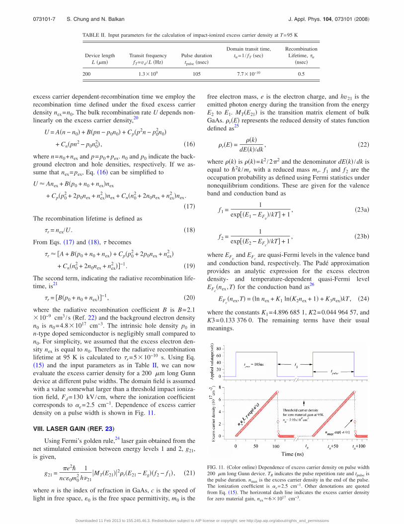
where the radiative recombination coefficient B is B=2.1�10−9 cm3 /s �Ref. 22� and the background electron densityn0 is n0=4.8�1017 cm−3. The intrinsic hole density p0 inn-type doped semiconductor is negligibly small compared ton0. For simplicity, we assumed that the excess electron den-sity nex is equal to n0. Therefore the radiative recombinationlifetime at 95 K is calculated to �r=5�10−10 s. Using Eq.�15� and the input parameters as in Table II, we can nowevaluate the excess carrier density for a 200 �m long Gunndevice at different pulse widths. The domain field is assumedwith a value somewhat larger than a threshold impact ioniza-tion field, Fd=130 kV /cm, where the ionization coefficientcorresponds to e=2.5 cm−1. Dependence of excess carrierdensity on a pulse width is shown in Fig. 11.
VIII. LASER GAIN „REF. 23…
Using Fermi’s golden rule,24 laser gain obtained from thenet stimulated emission between energy levels 1 and 2, g21,is given,
g21 =�e2�
nc0m02
1
h�21�MT�E21��2�r�E21 − Eg��f2 − f1� , �21�
where n is the index of refraction in GaAs, c is the speed oflight in free space, 0 is the free space permittivity, m0 is the
free electron mass, e is the electron charge, and hv21 is theemitted photon energy during the transition from the energyE2 to E1. MT�E21� is the transition matrix element of bulkGaAs. �r�E� represents the reduced density of states functiondefined as25
�r�E� =��k�
dE�k�/dk, �22�
where ��k� is ��k�=k2 /2�2 and the denominator dE�k� /dk isequal to �2k /mr with a reduced mass mr. f1 and f2 are theoccupation probability as defined using Fermi statistics undernonequilibrium conditions. These are given for the valenceband and conduction band as
f1 =1
exp��E1 − EFv�/kT� + 1
, �23a�
f2 =1
exp��E2 − EFc�/kT� + 1
, �23b�
where EFvand EFc
are quasi-Fermi levels in the valence bandand conduction band, respectively. The Padé approximationprovides an analytic expression for the excess electrondensity- and temperature-dependent quasi-Fermi levelEFc
�nex ,T� for the conduction band as26
EFc�nex,T� = �ln nex + K1 ln�K2nex + 1� + K3nex�kT , �24�
where the constants K1=4.896 685 1, K2=0.044 964 57, andK3=0.133 376 0. The remaining terms have their usualmeanings.
TABLE II. Input parameters for the calculation of impact-ionized excess carrier density at T=95 K
Device lengthL ��m�
Transit frequencyfT=vd /L �Hz�
Pulse durationtpulse �nsec�
Domain transit time,ttr=1 / fT �sec�
RecombinationLifetime, �tr
�nsec�
200 1.3�109 105 7.7�10−10 0.5
FIG. 11. �Color online� Dependence of excess carrier density on pulse width200 �m long Gunn device. TR indicates the pulse repetition rate and tpulse isthe pulse duration. nmax is the excess carrier density in the end of the pulse.The ionization coefficient is e=2.5 cm−1. Other denotations are quotedfrom Eq. �15�. The horizontal dash line indicates the excess carrier densityfor zero material gain, nex6�1017 cm−3.
073101-7 S. Chung and N. Balkan J. Appl. Phys. 104, 073101 �2008�
Downloaded 11 Feb 2013 to 155.245.46.3. Redistribution subject to AIP license or copyright; see http://jap.aip.org/about/rights_and_permissions
The charge neutrality condition �n= p� can be used forthe calculation of EFv
�p ,T� in the valence band. E1 of Eq.�23a� and E2 of Eq. �23b� are defined with assumption ofparabolic bands and the k-selection rule as
E1 = Ev − �E21 − Eg�mr
mv, �25a�
E2 = Ec − �E21 − Eg�mr
mc. �25b�
Taking into account energy uncertainty of the electron statescausing energy broadening, optical gain is determined withintegration over transitions contributing to the gain at thespecific photon energy E=hv0,
g�hv0� =� gmax�E21��f2 − f1�L�hv0 − E21�dE21, �26�
where gmax�Ecv� is the maximum material gain given in Eq.�21� and L�hv0−Ecv� is a Lorentzian lineshape function.
When losses in the cavity are taken into account thethreshold gain required for the lasing condition, �g�th, can beobtained as follows:27
��g�th = i + �1/L�ln�1/r1r2� , �27�
where the average internal loss of a cavity is i10 cm−1
and the mean mirror intensity reflection coefficient forGaAs-air interface is R=r1r20.32. Taking the optical con-finement �=1 and the device length L=200 �m, we find thelasing threshold gain ��g�th=67 cm−1.
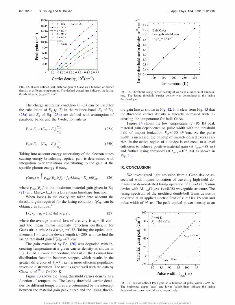
The gain evaluated by Eq. �26� was degraded with in-creasing temperature at a given carrier density as shown inFig. 12. At a lower temperature, the tail of the Fermi–Diracdistribution function becomes steeper, which results in thegreater difference of f2− f1, i.e., a more efficient populationinversion distribution. The results agree well with the data byChow et al.26 at T=300 K.
Figure 13 shows the lasing threshold carrier density as afunction of temperature. The lasing threshold carrier densi-ties for different temperatures are determined by the interceptbetween the material gain peak curve and the lasing thresh-
old gain line as shown in Fig. 12. It is clear from Fig. 13 thatthe threshold carrier density is linearly increased with in-creasing the temperature for bulk GaAs.
Figure 14 shows the low temperature �T=95 K� peakmaterial gain dependence on pulse width with the thresholdfield of impact ionization Fth=130 kV /cm. As the pulsewidth is increased, the buildup of impact-ionized excess car-riers in the active region of a device is enhanced to a levelsufficient to achieve positive material gain �at tpulse=88 ns�and further lasing threshold �at tpulse=105 ns� as shown inFig. 14.
IX. CONCLUSION
We investigated light emission from a Gunn device as-sociated with impact ionization of traveling high-field do-mains and demonstrated lasing operation of a GaAs FP Gunndevice with Al1−xBGaxAs �x=0.38� waveguide structure. Thelasing spectrum of the modified dumb-bell Gunn device isobserved at an applied electric field of F�3.83 kV /cm andpulse width of 95 ns. The peak optical power density at an
FIG. 12. �Color online� Peak material gain of GaAs as a function of carrierdensity at different temperatures. The dashed-dotted line indicates the lasingthreshold gain, �g�th=67 cm−1.
FIG. 13. Threshold lasing carrier density of GaAs as a function of tempera-ture. The lasing threshold carrier density was determined at the lasingthreshold gain.
FIG. 14. �Color online� Peak gain as a function of pulse width T=95 K.The horizontal upper �dash� and lower �solid� lines indicate the lasingthreshold and zero material gain, respectively.
073101-8 S. Chung and N. Balkan J. Appl. Phys. 104, 073101 �2008�
Downloaded 11 Feb 2013 to 155.245.46.3. Redistribution subject to AIP license or copyright; see http://jap.aip.org/about/rights_and_permissions

applied field of F=3.83 kV /cm is around 13.5 W /cm2 cor-responding to an emitted power of P=25.4 �W. Lasingfrom the Gunn device is due to band-to-band radiative re-combination of impact-ionized carriers inside high-field do-mains. A theoretical assessment showed that a threshold ex-cess carrier density for an inverted population distribution iscorrelated with an applied pulse width and electric field. Anumerical and analytic quantitative account of a lasingmodel was given using the following procedure:
�1� obtain the electron drift velocity-electric field curve us-ing the Monte Carlo method,
�2� obtain the maximum domain field from the unequal ar-eas rule,
�3� obtain the ionization rate from the theoretical curve, de-fined by the lucky-drift model, fitting the experimentaldata,
�4� model the initial buildup of light emission taking intoaccount the domain frequency, the accumulation effectof the additional excess carriers in the accumulationlayer of the domain, and the spontaneous recombinationrate in GaAs, and
�5� obtain the maximum material gain as a function of theapplied pulse width by using the gain spectrum includ-ing a lineshape function.
ACKNOWLEDGMENTS
We are grateful to the University of Essex for supportingthe project through the RPF.
1J. S. Heeks, IEEE Trans. Electron Devices 13, 68 �1966�.2N. Balkan and M. Hostut, Physica B �Amsterdam� 272, 291 �1999�.3S. Chung, A. Boland-Thoms, J. Y. Wah, N. Balkan, and B. K. Ridley,
Semicond. Sci. Technol. 19, S400 �2004�.4W. H. Hayt, Jr., Engineering Electromagnetics �McGraw-Hill, New York,1985�, p. 136.
5E. Kreyszig, Advanced Engineering Mathematics, 6th ed. �Wiley, NewYork, 1981�, p. 1029.
6B. K. Ridley, Semicond. Sci. Technol. 3, 542 �1988�.7C. H. Gooch, Gallium Arsenide Lasers �Wiley, London, 1969�, p. 104.8H. C. Casey, Jr. and M. B. Panish, Heterostructure Lasers �Academic,New York, 1978�, pp. 178–179.
9W. Fawcett, A. D. Boardman, and S. Swain, J. Phys. Chem. Solids 31,1963 �1970�.
10H. D. Rees, J. Phys. Chem. Solids 30, 643 �1969�.11H. L. Hartnagel, Gunn-Effect Logic Devices, 1st ed. �Heinemann Educa-
tional Books, London, 1973�, p. 25.12P. N. Butcher, W. Fawcett, and C. Hilsum, Br. J. Appl. Phys. 17, 841
�1966�.13H. L. Hartnagel, Gunn-Effect Logic Devices, 1st ed. �Heinemann Educa-
tional Books, London, 1973�, Chap. 2.14N. Balkan, B. K. Ridley, and A. J. Vickers, Negative Differential Resis-
tance and Instabilities in 2-D semiconductors �Plenum, New York, 1993�,pp. 215–249.
15E. Zanoni, L. Vendrame, P. Pavan, M. Manfredi, S. Bigliardi, R. Malik,and C. Canali, Appl. Phys. Lett. 62, 402 �1993�.
16B. K. Ridley, J. Phys. C 16, 3373 �1983�.17B. K. Ridley, J. Phys. C 16, 4733 �1983�.18J. Singh, Semiconductor Optoelectronics: Physics and Technology
�McGraw-Hill, Singapore, 1995�, p. 147.19P. P. Bohn and G. J. Herskowitz, IEEE Trans. Electron Devices 19, 14
�1972�.20R. N. Hall, Proc. Inst. Electr. Eng. 106B, 923 �1960�.21D. K. Schroder, Semiconductor Material and Device Characterization
�Wiley, New York, 1990�, p. 361.22Y. P. Varshni, Phys. Status Solidi 19, 459 �1967�.23L. A. Coldren and S. W. Corzine, Diode Lasers and Photonic Integrated
Circuits �Wiley, New York, 1995�, pp. 112–136.24Ibid, p. 508, 1995.25P. S. Zory, Jr., Quantum Well Lasers �Academic, San Diego, 1993�, p. 34.26W. W. Chow, S. W. Koch, and M. Sargent III, Semiconductor-Laser Phys-
ics �Springer-Verlag, Berlin, 1994�, p. 47.27L. A. Coldren and S. W. Corzine, Diode Lasers and Photonic Integrated
Circuits �Wiley, New York, 1995�, p. 39.
073101-9 S. Chung and N. Balkan J. Appl. Phys. 104, 073101 �2008�
Downloaded 11 Feb 2013 to 155.245.46.3. Redistribution subject to AIP license or copyright; see http://jap.aip.org/about/rights_and_permissions