Embed Size (px)
Citation preview
1 of 31
FORM DT-030 Iss 3 Product Specification | Product No: DMT070WSNLNT0-1A REV. A ©2018 Densitron Technologies Limited. All rights reserved. Proprietary data
TFT LCD DISPLAY MODULE
Product Specification
Customer Standard
Product Number
DMT070WSNLNT0-1A
Customer Part Number
Customer Approval
Date:
Internal Approvals
Product Mgr Doc. Control Electr. Eng.
Luo Luo Filip Kaczorowski Filip Kaczorowski
Date: 09/08/2018 Date: 09/08/18 Date: 09/08/18

2 of 31
FORM DT-030 Iss 3 Product Specification | Product No: DMT070WSNLNT0-1A REV. A ©2018 Densitron Technologies Limited. All rights reserved. Proprietary data
Revision Record
Rev. Date Page Chapt. Comment ECR no.
A 09/08/18 -- -- Initial Release

3 of 31
FORM DT-030 Iss 3 Product Specification | Product No: DMT070WSNLNT0-1A REV. A ©2018 Densitron Technologies Limited. All rights reserved. Proprietary data
Table of Contents
1.0 GENERAL DESCRIPTION 5
1.1 Introduction 5
1.2 Main Features 5
2.0 MECHANICAL SPECIFICATION 6
2.1 Mechanical Characteristics 6
2.2 Mechanical Drawing 7
3.0 ELECTRICAL SPECIFICATION 8
3.1 Absolute Maximum Ratings 8 3.1.1 TFT 8
3.2 Electrical Characteristics 8
3.4 Interface Pin Assignment 9
3.5 Block Diagram 12
3.6 Timing Characteristics 13 3.6.1 AC Electrical Characteristics 13 3.6.2 Input Clock and Data Timing Diagram 13 3.6.3 DC Electrical Characteristics 14 3.6.4 Timing 14 3.6.5 Data Input Format 15 3.6.6 Reset Timing Characteristics 15
4.0 OPTICAL SPECIFICATION 17
4.1 Optical Characteristics 17
5.0 LED BACKLIGHT SPECIFICATION 19
5.1 LED Backlight Characteristics 19
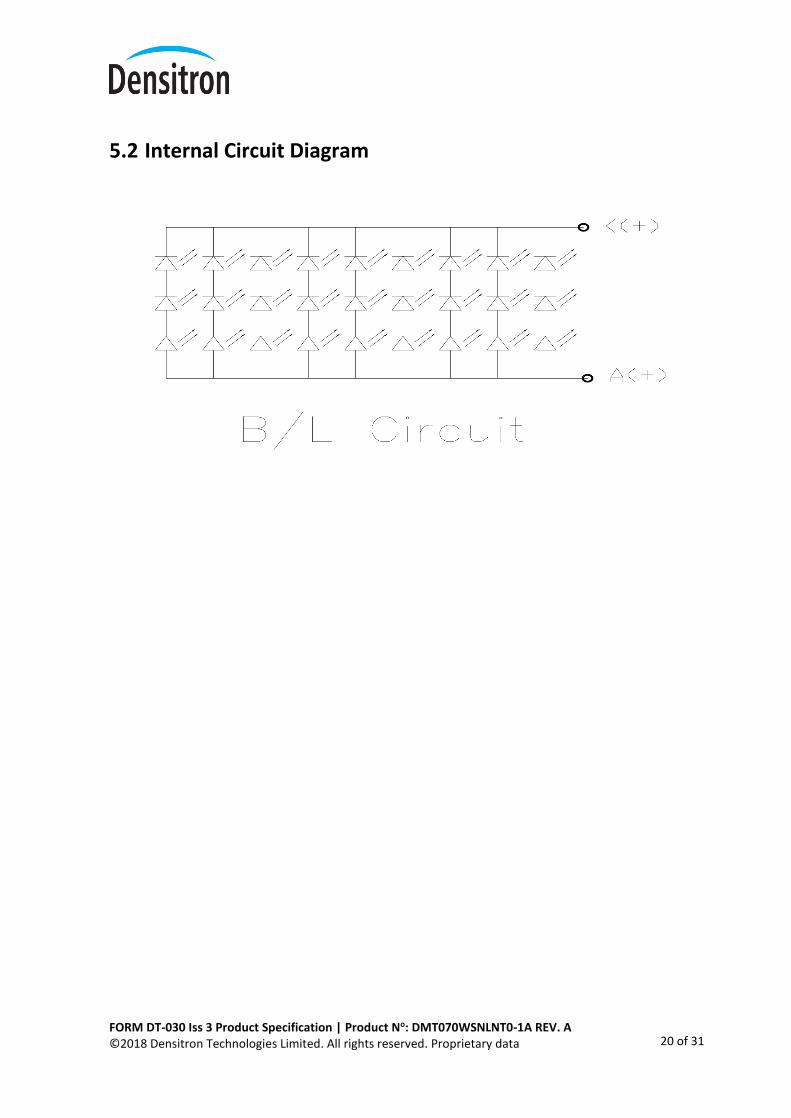
5.2 Internal Circuit Diagram 20
6.0 QUALITY ASSURANCE SPECIFICATION 21
6.1 Delivery Inspection Standards 21

4 of 31
FORM DT-030 Iss 3 Product Specification | Product No: DMT070WSNLNT0-1A REV. A ©2018 Densitron Technologies Limited. All rights reserved. Proprietary data
6.1.1 Inspection Conditions 21 6.1.2 Environmental Conditions 21 6.1.3 Sampling Conditions 21 6.1.4 Zone Definition 22 6.1.5 Basic Principle 22 6.1.6 Inspection Criteria 23
6.2 Dealing with Customer Complaints 27 6.2.1 Non-conforming Analysis 27 6.2.2 Handling of Non-conforming Displays 27
7.0 RELIABILITY SPECIFICATION 28
7.1 Reliability Tests 28
8.0 HANDLING PRECAUTIONS 29
8.1 Handling Precautions 29
8.2 Storage Precautions 30
8.3 Designing Precautions 30
8.4 Operation Precautions 31
8.5 Other Precautions 31

5 of 31
FORM DT-030 Iss 3 Product Specification | Product No: DMT070WSNLNT0-1A REV. A ©2018 Densitron Technologies Limited. All rights reserved. Proprietary data
1.0 General Description
1.1 Introduction This is a colour active matrix TFT (Thin Film Transistor) LCD (liquid crystal display) that uses amorphous silicon TFT as a switching device. This module is composed of a Transmissive type TFT-
LCD Panel, driver circuit, capacitance touch panel back-light unit. The resolution of a 7.0” TFT-LCD contains 1024x600 pixels and can display up to 16.7M colours.
1.2 Main Features
Item Contents
Screen Size 7.0” Diagonal
Display Format 1024 x RGB x 600 Dots
N° of Colour 262K/16.7M
Overall Dimensions 165.00 mm (H) x 100.00 mm (V) x 5.8 mm (D)
Active Area 154.21 mm (H) x 85.92 mm (V)
Display Mode Transmissive / Normally Black
Viewing Direction All round
TFT Interface 6/8Bit LVDS
Touch mode Ten points and Gestures
TFT Driver IC EK73215& EK79001
Backlight Type LED, White, 27 chips
Operating Temperature -20C ~ +70°C
Storage Temperature -30°C ~ +80°C
ROHS Compliant to 2011/65/EU

6 of 31
FORM DT-030 Iss 3 Product Specification | Product No: DMT070WSNLNT0-1A REV. A ©2018 Densitron Technologies Limited. All rights reserved. Proprietary data
2.0 Mechanical Specification
2.1 Mechanical Characteristics
Item Characteristic Unit
Display Format 1024 x RGB x 600 Dots Dots
Overall Dimensions 165.00 mm (H) x 100.00 mm (V) x 5.8 mm (D) mm
Active Area 154.21 mm (H) x 85.92 mm (V) mm
Pixel Pitch 0.1506 (H) x 0.1432 (V) mm
Weight 142 g

7 of 31
FORM DT-030 Iss 3 Product Specification | Product No: DMT070WSNLNT0-1A REV. A ©2018 Densitron Technologies Limited. All rights reserved. Proprietary data
2.2 Mechanical Drawing

8 of 31
FORM DT-030 Iss 3 Product Specification | Product No: DMT070WSNLNT0-1A REV. A ©2018 Densitron Technologies Limited. All rights reserved. Proprietary data
3.0 Electrical Specification
3.1 Absolute Maximum Ratings
3.1.1 TFT
Item Symbol Min. Max. Unit Note
Power Supply Voltage VDD -0.3 3.6 V 1
Operating Temperature TOP -20 +70 °C -
Storage Temperature TST -30 +80 °C -
(Ta=25 VSS=0V) Note 1: If the absolute maximum rating of even is one of the above parameters is exceeded even momentarily, the quality of the product may be degraded. Absolute maximum ratings, therefore, specify the values exceeding which the product may be physically damaged. Be sure to use the product within the range of the absolute maximum ratings.
3.2 Electrical Characteristics
Item Symbol Min. Typ. Max. Unit
Supply Voltage VDD 3.0 3.3 3.6 V
Normal mode Current IDD -- 120 -- mA
High Level Input VIH 0.7xVDD - VDD V
Low Level Input VIL GND - 0.3xVDD V
High Level Output VOH VDD-0.4 - VDD V
Low Level Output VOL GND - 0.4 V

9 of 31
FORM DT-030 Iss 3 Product Specification | Product No: DMT070WSNLNT0-1A REV. A ©2018 Densitron Technologies Limited. All rights reserved. Proprietary data
3.4 Interface Pin Assignment
No. Symbol Function
1 NC Not Connected. These pins are left not connected.
2 VDD Digital supply voltage.
3 VDD Digital supply voltage.
4 NC Not Connected. These pins are left not connected.
5 RESET Global reset pin. Active low to ender reset state.
6 STBYB
Standby mode, Normally puled high STBYB = ‘1’, normal mode operation STBYB = ‘0’, timing controller, source driver will turn off, all output are High-Z
7 GND Ground of Logic Circuit. This is a ground pin, to be connected to external ground.
8 RXIN0- Negative LVDS differential data input.
9 RXIN0+ Positive LVDS differential data input.
10 GND Ground of Logic Circuit. This is a ground pin, to be connected to external ground.
11 RXIN1- Negative LVDS differential data input.
12 RXIN1+ Positive LVDS differential data input.
13 GND Ground of Logic Circuit. This is a ground pin, to be connected to external ground.
14 RXCLKIN- Negative LVDS differential clock input.
15 RXCLKIN+ Positive LVDS differential clock input.
16 GND Ground of Logic Circuit. This is a ground pin, to be connected to external ground.
17 RXIN2- Negative LVDS differential data input.
18 RXIN2+ Positive LVDS differential data input.
19 GND Ground of Logic Circuit. This is a ground pin, to be connected to external ground.
20 RXIN3- Negative LVDS differential data input.
21 RXIN3+ Positive LVDS differential data input.

10 of 31
FORM DT-030 Iss 3 Product Specification | Product No: DMT070WSNLNT0-1A REV. A ©2018 Densitron Technologies Limited. All rights reserved. Proprietary data
No. Symbol Function
22 GND Ground of Logic Circuit. This is a ground pin, to be connected to external ground.
23 NC Not Connected. These pins are left not connected.
24 NC Not Connected. These pins are left not connected.
25 GND Ground of Logic Circuit. This is a ground pin, to be connected to external ground.
26 NC Not Connected. These pins are left not connected.
27 DIMO
Backlight dimmer signal for external controller. DIMO = ‘0’, Turn off external backlight controller DIMO = ‘1’, Logical control signal to turn on external backlight controller NOTE: If CABC OFF, DIMO = DIMI. Else DIMO is controlled by CABC If not used leave open.
28 SELB Input data format selection. SLEB = ‘0’, 8-Bit LVDS. SLEB = ‘1’ 6-Bit LVDS.
29 NC Not Connected. These pins are left not connected.
30 GND Ground of Logic Circuit. This is a ground pin, to be connected to external ground.
31 LED- LED backlight Negative Supply pin. These pins are to be connected to external source.
32 LED- LED backlight Negative Supply pin. These pins are to be connected to external source.
33 L/R Horizontal shift direction. (Note 1)
34 U/D Vertical shift direction. (Note 1)
35 NC Not Connected. These pins are left not connected.
36 NC Not Connected. These pins are left not connected.
37 NC Not Connected. These pins are left not connected.
38 NC Not Connected. These pins are left not connected.
39 LED+ LED backlight Positive Supply pin. These pins are to be connected to external source.

11 of 31
FORM DT-030 Iss 3 Product Specification | Product No: DMT070WSNLNT0-1A REV. A ©2018 Densitron Technologies Limited. All rights reserved. Proprietary data
No. Symbol Function
40 LED+ LED backlight Positive Supply pin. These pins are to be connected to external source.
Note 1: When L/R=’0’, set right to left scan direction. When L/R=’1’, set left to right scan direction. When U/D=’0’, set top to bottom scan direction. When U/D=’1’ set bottom to top scan direction.

12 of 31
FORM DT-030 Iss 3 Product Specification | Product No: DMT070WSNLNT0-1A REV. A ©2018 Densitron Technologies Limited. All rights reserved. Proprietary data
3.5 Block Diagram

13 of 31
FORM DT-030 Iss 3 Product Specification | Product No: DMT070WSNLNT0-1A REV. A ©2018 Densitron Technologies Limited. All rights reserved. Proprietary data
3.6 Timing Characteristics 3.6.1 AC Electrical Characteristics
Parameter Symbol Min. Typ. Max. Unit Clock frequency RxFCLK 40.8 51.2 67.2 MHz
Input data skew margin TRSKM 500 - - ps
Clock high time TLVCH - 4/(7x RxFCLK ) - ns
Clock low time TLVCL - 3/(7x RxFCLK) - ns
3.6.2 Input Clock and Data Timing Diagram

14 of 31
FORM DT-030 Iss 3 Product Specification | Product No: DMT070WSNLNT0-1A REV. A ©2018 Densitron Technologies Limited. All rights reserved. Proprietary data
3.6.3 DC Electrical Characteristics Parameter Symbol Min. Max. Unit Remark
Differential input high Threshold voltage
RxVTH - +0.1 V RXVCM1.2V
Differential input low Threshold voltage
RxVTL -0.1 - V
Input voltage range (singled-end)
RxVIN 0 2.4 V
Differential input common mode voltage
RxVCM |VID|/2 2.4-|VID|/2 V
Differential voltage |VID| 0.2 0.6 V
Differential input leakage current
RVxliz -10 +10 µA
3.6.4 Timing
Parameter Symbol Min. Typ. Max. Unit Remark
Clock frequency fclk 40.8 51.2 67.2 MHz Frame rate
=60Hz
Horizontal display area
thd 1024 DCLK
HS period time th 1114 1344 1400 DCLK
HS Blanking thb 90 320 376 DCLK
Vertical display area
tvd 600 H
VS period time tv 610 635 800 H
VS Blanking thb 10 35 200 H

15 of 31
FORM DT-030 Iss 3 Product Specification | Product No: DMT070WSNLNT0-1A REV. A ©2018 Densitron Technologies Limited. All rights reserved. Proprietary data
3.6.5 Data Input Format • 6-Bit LVDS input
• 8-Bit LVDS input
Note: Support DE timing mode only, SYNC mode not supported.
3.6.6 Reset Timing Characteristics

16 of 31
FORM DT-030 Iss 3 Product Specification | Product No: DMT070WSNLNT0-1A REV. A ©2018 Densitron Technologies Limited. All rights reserved. Proprietary data
Note 1: The reset cancel includes also required time for loading ID bytes. VCOM setting and other settings from EEPROM to registers. This loading is done every time when there is HW reset cancel time (tRT) within 5 ms after rising edge of RESX. Note 2: Spike due to an electrostatic discharge on RESX line dose not because irregular system reset according to the table below:
Note 3: During the resetting period, the display will be blanked (The display is entering blanking sequence, which maximum time is 120ms, when reset starts in Sleep Out-mode. The display remains the blank state in Sleep In-mode.) and then return to default condition for Hardware Reset. Note 4: Spike rejection also applies during a valid reset pulse as shown below:
Note 5: When reset applied during Sleep in Mode. Note 6: When reset applied during Sleep out Mode. Note 7: It is necessary to wait 5msec after releasing RESX before sending commands. Also Sleep Out command cannot be sent for 120msec.

17 of 31
FORM DT-030 Iss 3 Product Specification | Product No: DMT070WSNLNT0-1A REV. A ©2018 Densitron Technologies Limited. All rights reserved. Proprietary data
4.0 Optical Specification
4.1 Optical Characteristics Measuring instruments: LCD-5100, Eldim, Topcon BM-7 Driving condition: VDD = 3.3V, VSS = 0V Backlight: IF = 75mA Measured temperature: Ta = 25°C
Characteristics Symbol Conditions Min Typ Max Unit Note
Response time TR+TF θ=Ф=0° Normal
Viewing Angle
- 25 40 ms 2
Contrast Ratio CR 600 800 - - 3
Uniformity S(%) - 50 - %
Vie
win
g A
ngl
e Left θL
CR≥10
- 85 -
deg 4 Right θR - 85 -
Up θU - 85 -
Down θD - 85 -
Co
lou
r C
hro
mat
icit
y
Red Rx
CR≥10
0.5758 0.6158 0.6558
- 5
Ry 0.2915 0.3315 0.3715
Green Gx 0.2907 0.3315 0.3715
Gy 0.5345 0.5745 0.6145
Blue Bx 0.1066 0.1466 0.1866
By 0.0738 0.1138 0.1538
White Wx 0.2668 0.0368 0.3468
Wy 0.2984 0.3384 0.3784
Option View Direction All

18 of 31
FORM DT-030 Iss 3 Product Specification | Product No: DMT070WSNLNT0-1A REV. A ©2018 Densitron Technologies Limited. All rights reserved. Proprietary data
Note Item Test method
1 Setup
The display should be stabilised at a given temperature for 30 minutes to avoid abrupt temperature change during measuring. To stabilise the luminance, measurements should be executed after lighting the backlight for 30 minutes in a windless room.
2 Response time
Measure output signal waveform by the luminance meter when raster of window pattern is changed from white to black and from black to white.
3 Contrast ratio
Measure maximum brightness and minimum brightness at the centre of the screen by displaying raster or window pattern. Then calculate the ratio between these two values. Brightness of unselected position (white) Contrast Ratio (CR) = Brightness of selected position (black)
4 Viewing angle Horizontal θ Vertical Ø
Move the luminance meter from right to left and up and down and determinate the angles where contrast ratio is 10
5 Colour chromaticity Measure chromaticity coordinates x and y of CIE1931 colorimetric system
6 Brightness distribution
(Brightness distribution) = 100 x B/A % A: max. brightness of the 9 points B: min. brightness of the 9 points

19 of 31
FORM DT-030 Iss 3 Product Specification | Product No: DMT070WSNLNT0-1A REV. A ©2018 Densitron Technologies Limited. All rights reserved. Proprietary data
5.0 LED Backlight Specification
5.1 LED Backlight Characteristics The back-light system is edge-lighting type with 27 chips LED
Characteristics Symbol Min Typ. Max Unit Note
Forward Current IF 180 270 - mA -
Forward Voltage VF - 9.6 - V -
LCM Luminance at 180mA LV 350 420 - Cd/m2 3
LCM Luminance at 270mA LV 550 600 - Cd/m2 3
LED life time Hr - 50000 - Hour 1,2
Uniformity Avg 80 - - % 3
Note 1: LED life time (Hr) can be defined as the time in which it continues to operate under the condition: Ta=25±3 ℃, typical IL value indicated in the above table until the brightness becomes less than 50%. Note 2: The “LED life time” is defined as the module brightness decrease to 50% original brightness at Ta=25℃ and IL=80mA. The LED lifetime could be decreased if operating IL is larger than 80mA. The constant current driving method is suggested. Note 3: Luminance Uniformity of these 9 points is defined as below:
20 of 31
FORM DT-030 Iss 3 Product Specification | Product No: DMT070WSNLNT0-1A REV. A ©2018 Densitron Technologies Limited. All rights reserved. Proprietary data
5.2 Internal Circuit Diagram

21 of 31
FORM DT-030 Iss 3 Product Specification | Product No: DMT070WSNLNT0-1A REV. A ©2018 Densitron Technologies Limited. All rights reserved. Proprietary data
6.0 Quality Assurance Specification
6.1 Delivery Inspection Standards
6.1.1 Inspection Conditions Inspection distance: 30 cm - 50cm Viewing angle: ±45°
6.1.2 Environmental Conditions Ambient temperature: 25°C ± 5°C Ambient humidity: 65±10% RH Ambient illumination: 300~700 lux
6.1.3 Sampling Conditions 1. Lot size: quantity of shipment lot per model 2. Sampling method:
Sampling plan GB/T 2828-2003
Normal inspection, Class II
AQL Major Defect 0.65%
Minor Defect 1.5%
No. Items to be inspected
Criteria Classification
of defects
1 Functional defects
1) No display, Open or miss line 2) Display abnormally, Short 3) Backlight no lighting, abnormal lighting. 4) TP no function Major
2 Missing Missing component
3 Outline dimension Overall outline dimension beyond the
drawing is not allowed
4 Colour tone Colour unevenness, refer to limited sample
Minor 5 Spot Line defect
Light dot, Dim spot, Polarizer bubble; Polarizer accidented spot.
6 Soldering appearance Good soldering, peeling off is not allowed.
7 LCD/Polarizer/TP Black/White spot/line, scratch, crack, etc.

22 of 31
FORM DT-030 Iss 3 Product Specification | Product No: DMT070WSNLNT0-1A REV. A ©2018 Densitron Technologies Limited. All rights reserved. Proprietary data
6.1.4 Zone Definition
Zone A: Effective Viewing Area (Character or Digit can be seen) Zone B: Viewing Area except Zone A Zone C: Outside (ZoneA+ZoneB) which can’t be seen after assembly by customer. Zone D: IC Bonding Area Note: Generally, visual defects in Zone C can be ignored when it doesn’t affect product function or appearance after assembly by customer.
6.1.5 Basic Principle A set of sample to indicate the limit of acceptable quality level shall be discussed should a dispute occur.

23 of 31
FORM DT-030 Iss 3 Product Specification | Product No: DMT070WSNLNT0-1A REV. A ©2018 Densitron Technologies Limited. All rights reserved. Proprietary data
6.1.6 Inspection Criteria
Number Items Criteria (mm)
1.0 LCD Crack/ Broken
Note: X: Length Y: Width Z: Height L: Length of ITO T: Height of LCD
(1) The edge of
LCD broken
X Y Z
≤3.0mm <Inner border line of the seal
≤T
(2) LCD corner broken
X Y Z
≤3.0mm ≤L ≤T
(3) LCD crack

24 of 31
FORM DT-030 Iss 3 Product Specification | Product No: DMT070WSNLNT0-1A REV. A ©2018 Densitron Technologies Limited. All rights reserved. Proprietary data
Number Items Criteria (mm)
2.0 Spot defects
Φ=(X+Y)/2
① Light dot (LCD/TP/Polarizer black/white spot, light dot, pinhole, dent, stain)
Size (mm) Zone Acceptable Qty
A B C
Φ≤0.10 Ignore
Ignore 0.10<Φ≤0.25 4(distance≧10mm)
0.25<Φ≤0.35 3
Φ>0.4 0
②Dim spot (LCD/TP/Polarizer dim dot, light leakage, dark spot)
Size (mm) Zone Acceptable Qty
A B C
Φ≤0.1 Ignore
Ignore 0.10<Φ≤0.25 4(distance≧10mm)
0.25<Φ≤0.35 3
Φ>0.40 0
③ Polarizer accidented spot
Size (mm) Zone Acceptable Qty
A B C
Φ≤0.2 Ignore
Ignore 0.3<Φ≤0.5 3(distance≧10mm)
Φ>0.5 1
④ Pixel bad points (light dot, Dim dot, colour dot)
Size (mm) Zone Acceptable Qty
A B C
Φ≤0.15 Ignore
Ignore 0.2<Φ≤0.3 2(distance≧1
0mm)
Φ>0.4 1
⑤ Polarizer Bubble
Size (mm) Zone Acceptable Qty
A B C
Φ≤0.2 Ignore
Ignore 0.3<Φ≤0.4 4(distance≧10mm)
0.4<Φ≤0.5 3
Φ>0.5 1
X
Y

25 of 31
FORM DT-030 Iss 3 Product Specification | Product No: DMT070WSNLNT0-1A REV. A ©2018 Densitron Technologies Limited. All rights reserved. Proprietary data
3.0 Line
defect (LCD/TP/ Polarizer
black/ white line,
scratch, stain)
Width (mm) Length (mm) Acceptable Qty
A B C
Φ≤0.05 Ignore Ignore
Ignore 0.05<W≤0.06 L≤5.0 N≤2
0.07<W≤0.08 L≤4.0 N≤2
0.08<W Define as spot defect
4.0 SMT
Do not allow: missing parts, solderless connection, cold solder joint, miss match, the positive and negative polarity oppose
5.0 Display colour & Brightne
ss
1. Colour: Measuring the colour coordinates, The measurement standard according to the datasheet or samples
2. Brightness: Measuring the brightness of White screen, The measurement standard according to the datasheet or Samples
6.0 LCD Mura
By 5% ND filter invisible
7.0 RTP Related
TP bubble / accidented spot
Size Φ(mm)
Zone Acceptable Qty
A B C
Φ≤0.1 Ignore
Ignore 0.1<Φ≤0.25 4(distance≧ 10mm)
0.25<Φ≤0.35 3
0.4<Φ 1
TP film scratch
Width(mm) Length (mm)
Acceptable Qty
A B C
Φ≤0.05 Ignore Ignore
Ignore 0.05<W≤0.06 L≤5.0 N≤3
0.07<W≤0.08 L≤4.0 N≤2
0.08<W Define as spot defect
Assembly deflection
Beyond the edge of backlight ≤0.2mm
Bulge (undulation
included)
The ITO film plumped below 0.40mm is acceptable

26 of 31
FORM DT-030 Iss 3 Product Specification | Product No: DMT070WSNLNT0-1A REV. A ©2018 Densitron Technologies Limited. All rights reserved. Proprietary data
Number Items Criteria (mm)
5.0 RTP Related
Newton Ring
Newton Ring area>1/3 TP area not acceptable Newton Ring area≤1/3 TP area acceptable
TP corner broken X: length Y: Width Z: Height
X Y Z
X≤3.0mm
Y≤3.0mm
Z< LCD thickness
Circuitry broken is not allowed
TP edge broken X: length Y: Width Z: Height
X Y Z
X≤6.0mm
Y≤2.0mm
Z< LCD thickness
Circuitry broken is not allowed
• Criteria (functional items)
Number Items Criteria
1 No display Not allowed
2 Missing segment Not allowed
3 Short Not allowed
4 Backlight no lighting Not allowed
5 TP no function Not allowed

27 of 31
FORM DT-030 Iss 3 Product Specification | Product No: DMT070WSNLNT0-1A REV. A ©2018 Densitron Technologies Limited. All rights reserved. Proprietary data
6.2 Dealing with Customer Complaints
6.2.1 Non-conforming Analysis Purchaser should supply Densitron with detailed data of non-conforming sample. After accepting it, Densitron should complete the analysis in two weeks from receiving the sample. If the analysis cannot be completed on time, Densitron must inform the purchaser.
6.2.2 Handling of Non-conforming Displays If any non-conforming displays are found during customer acceptance inspection which Densitron is clearly responsible for, return them to Densitron. Both Densitron and customer should analyse the reason and discuss the handling of non-conforming displays when the reason is not clear. Equally, both sides should discuss and come to agreement for issues pertaining to modification of Densitron quality assurance standard.

28 of 31
FORM DT-030 Iss 3 Product Specification | Product No: DMT070WSNLNT0-1A REV. A ©2018 Densitron Technologies Limited. All rights reserved. Proprietary data
7.0 Reliability Specification
7.1 Reliability Tests
Test Item Test Condition Sample
Size
High Temperature Operation Ta= 70°C 96 h 3pcs
Low Temperature Operation Ta = -20°C 96 h 3pcs
High Temperature Storage Tp = 80°C 96 h 3pcs
Low Temperature Storage Tp = -30°C 96 h 3pcs
High Temperature & High Humidity Storage
60°C, 90% RH 96 h 3pcs
Thermal Shock (Non-operation) -30℃,30 min ↔ 80℃,30 min,
Change time:5min 20CYC. 3pcs
ESD test C=150pF, R=330,5points/panel
Air: ±8KV, 5times; Contact: ±6KV, 5 times; (Environment: 15℃~35℃, 30%~60%).
3pcs
Vibration (Non-operation)
Frequency range:10~55Hz, Stroke:1.5mm Sweep:10Hz~55Hz~10Hz 2 hours for each
direction of X.Y.Z. (6 hours for total) (Package
condition).
3pcs
Box Drop Test 1 Corner 3 Edge 6 faces,
80 cm (Medium Box) 1 box
Note: Ta = ambient temperature, Tp= panel temperature Notes: 1. No dew condensation to be observed. 2. The function test shall be conducted after 4 hours storage at the normal temperature and humidity after removed from the test chamber. 3. No cosmetic or functional defects should be allowed. 4. Total current consumption should be less than twice the initial value.

29 of 31
FORM DT-030 Iss 3 Product Specification | Product No: DMT070WSNLNT0-1A REV. A ©2018 Densitron Technologies Limited. All rights reserved. Proprietary data
8.0 Handling Precautions
8.1 Handling Precautions
1) Since the display panel is being made of glass, do not apply mechanical impacts such us dropping from a high position.
2) If the display panel is broken by some accident and the internal organic substance leaks out, be careful not to inhale nor lick the organic substance.
3) If the liquid crystal touches your skin or clothes, wash it off immediately using soap and plenty of water
4) If pressure is applied to the display surface or its neighbourhood of the display module, the cell structure may be damaged and be careful not to apply pressure to these sections.
5) The polarizer covering the surface of the display module is soft and easily scratched. Please be careful when handling the display module.
6) When the surface of the polarizer of the display module has soil, clean the surface. It takes advantage of by using following adhesion tape.
a. Scotch Mending Tape No. 810 or an equivalent 2. Never try to breathe upon the soiled surface nor wipe the surface using cloth containing
solvent such as ethyl alcohol, since the surface of the polarizer will become cloudy. 3. Also, pay attention that the following liquid and solvent may spoil the polarizer:
• Water
• Ketone
• Aromatic Solvents 7) Hold the display module very carefully when placing it into the system housing. Do not
apply excessive stress or pressure to display module. And, do not over bend the film with electrode pattern layouts. These stresses will influence the display performance. Also, secure sufficient rigidity for the outer cases.
8) Do not apply stress to the LSI chips and the surrounding molded sections. 9) Do not disassemble nor modify the display module. 10) Do not apply input signals while the logic power is off. 11) Pay sufficient attention to the working environments when handing display modules to
prevent occurrence of element breakage accidents by static electricity.
• Be sure to make human body grounding when handling display modules.
• Be sure to ground tools to use or assembly such as soldering irons.
• To suppress generation of static electricity, avoid carrying out assembly work under dry environments.
30 of 31
FORM DT-030 Iss 3 Product Specification | Product No: DMT070WSNLNT0-1A REV. A ©2018 Densitron Technologies Limited. All rights reserved. Proprietary data
• Protective film is being applied to the surface of the display panel of the display module. Be careful since static electricity may be generated when exfoliating the protective film.
12) Protection film is being applied to the surface of the display panel and removes the protection film before assembling it. If the display module has been stored for a long period of time, residue adhesive material of the protection film may remain on the surface of the display panel after removed of the film. In such case, remove the residue material by the method introduced in the above Section 5).
13) If electric current is applied when the display module is being dewed or when it is placed under high humidity environments, the electrodes may be corroded and be careful to avoid the above.
8.2 Storage Precautions
1) When storing display modules, put them in static electricity preventive bags avoiding exposure to direct sun light nor to lights of fluorescent lamps, etc. and, also, avoiding high temperature and high humidity environments or low temperature (less than 0°C) environments. (We recommend you to store these modules in the packaged state when they were shipped from Densitron) At that time, be careful not to let water drops adhere to the packages or bags nor let dewing occur with them.
2) If electric current is applied when water drops are adhering to the surface of the display module, when the display module is being dewed or when it is placed under high humidity environments, the electrodes may be corroded and be careful about the above.
8.3 Designing Precautions 1) The absolute maximum ratings are the ratings which cannot be exceeded for display
module, and if these values are exceeded, panel damage may be happen. 2) To prevent occurrence of malfunctioning by noise, pay attention to satisfy the VIL and VIH
specifications and, at the same time, to make the signal line cable as short as possible. 3) We recommend you to install excess current preventive unit (fuses, etc.) to the power
circuit (VDD). (Recommend value: 0.5A) 4) Pay sufficient attention to avoid occurrence of mutual noise interference with the
neighbouring devices. 5) As for EMI, take necessary measures on the equipment side basically. 6) When fastening the display module, fasten the external plastic housing section. 7) If power supply to the display module is forcibly shut down by such errors as taking out the
main battery while the display panel is in operation, we cannot guarantee the quality of this display module.

31 of 31
FORM DT-030 Iss 3 Product Specification | Product No: DMT070WSNLNT0-1A REV. A ©2018 Densitron Technologies Limited. All rights reserved. Proprietary data
8.4 Operation Precautions
1) It is indispensable to drive the display within the specified voltage limit since excessive voltage shortens its life.
2) Direct current causes an electrochemical reaction with remarkable deterioration of the display quality. Consider prevent direct current during ON/OFF timing and during operation.
3) Response time is extremely delayed at temperatures lower than the operating temperature range while, at high temperatures, displays become dark. However, this phenomenon is reversible and does not mean a malfunction or a display that has been permanently damaged.
4) To protect display modules from performance drops by static electricity rapture, etc., do not touch the following sections whenever possible while handling the display modules.
• Pins and electrodes
• Pattern layouts such as the FPC 5) When the driver is being exposed (COG), semiconductor elements change their
characteristics when light is radiated according to the principle of the solar battery. Consequently, if the driver is exposed to light, malfunctioning may occur.
• Design the product and installation method so that the driver may be shielded from light in actual usage.
• Design the product and installation method so that the driver may be shielded from light during the inspection processes.
6) Although the display module stores the operation state data by the commands and the indication data, when excessive external noise, etc. enters the module, the internal status may be changed. It therefore is necessary to take appropriate measures to suppress noise generation or to protect from influences of noise on the system design.
7) We recommend you construct its software to make periodical refreshment of the operation statuses (re-setting of the commands and re-transference of the display data) to cope with catastrophic noise.
8.5 Other Precautions
1) Request the qualified companies to handle industrial wastes when disposing of the display modules. Or, when burning them, be sure to observe the environmental and hygienic laws and regulations.