Embed Size (px)
Citation preview

Terahertz Travelling Wave Amplifier Design using Ballistic Deflection Transistor
Huan Wang1, 2, Jean-François Millithaler1, Ronald W.Knepper2, Martin Margala1
1University of Massachusetts, 1 University Ave., Lowell, MA USA 2Boston University, 8 Saint Mary’s Street, Boston, MA USA
1E-mail: [email protected]
Abstract In this paper, we present a Terahertz (THz) Travelling-
Wave-Amplifier (TWA) design using a Ballistic Deflection Transistor (BDT). The BDT is an emerging functional device based on InGaAs/InAlAs/InP, which can operate at THz frequencies. A transistor model is proposed, based on data provided by Monte Carlo simulation. We have developed a new nearly lossless THz transmission line (0.46dB/mm over 0.8-1.5THz simulated in ANSYS HFSS), called Parallel Plate Dielectric Waveguide with Signal line (PPDWS), and we are able to design a 24-stage BDT TWA with an ADS simulated gain over 10dB at 1-1.5THz. This THz BDT amplifier design opens up new possibilities by increasing the speed by 100 times compared to existing technologies.
Keywords Terahertz, Travelling-Wave-Amplifier, BDT, PPDWS
1. Introduction These recent years have a seen a growing interest in
Terahertz (THz) frequencies. Because of the high frequency (0.3-3THz), this radiation has some unique characteristics: (1) the ability to penetrate most insulators such as paper and plastic; (2) the capability to carry large amount of data; (3) the possibility to reach Terabit per second. Therefore THz technologies are highly attractive in sensing[1], imaging [2], biomedical [3], telecommunications [4] and so on.
The main technology challenge is to reach the THz domain that is located between the operating regions of traditional electronics and optics in the electromagnetic spectrum. Although we have existing technologies such as standard millimeter-wave devices and infrared photonic devices, neither of them are suitable for THz operations. For THz sources, the present approach is frequency multiplexing from microwave sources or down-conversion from the optical domain using photo-misers. None of these methods is efficient, so the resulting output power of current available THz sources is very low. In addition there is a lack of suitable THz band amplifiers with sufficient gain and low noise temperature. By reviewing all the existing research, the results of sub-millimeter integrated (S-MMIC) circuit design is shown in Table 1. BDT devices are reported to be operated at more than 1THz (fT≥1.2THz) [13].Through the comparison with all the other reported S-MMIC amplifier design results, none of them are able to reach the real 1 THz region. We propose here to use a novel transistor based amplifier, which theoretically has a gain of more than 10 dB over 1 THz. Our simulation results show that the Ballistic Deflection Transistor (BDT) is very competitive with the existing
technologies. The highest frequency performing HEMT based amplifier in the list show a working frequency at 850GHz with a gain of 6dB, which is almost 2 times less than our projected gain for BDT based amplifier working at 1THz.
Table 1: Comparison of reported S-MMIC amplifiers and our proposed work
Frequency(THz) Gain(dB) Substrate Device Ref. 0.29 17.3 InP HBT [5] 0.32 15 InP HEMT [6]
0.325 20 InP HBT [7] 0.3 17 InP HEMT [8]
0.46 16.1 GaAs mHEMT [9] 0.55 10 InP HEMT [10] 0.65 20 InP HBT [11] 0.85 6 InP HEMT [12]
1 >10 InP BDT This work
Important electrical quantities necessary for this research, like transconductance (gm), internal capacitance and contact resistance, have been determined by means of Monte Carlo (MC) simulation. Our MC software can correctly reproduce the complex non-linear bell-shape I-V characteristic of the BDT and is of great importance for this work. In order to build the entire TWA system, a nearly lossless THz transmission line called the Parallel Plate Dielectric Waveguide with Signal Line (PPDWS) [14] is developed. We study the results in Advanced Design System (ADS).
2. Ballistic Deflection Transistor The BDT is an interesting device based on an
InGaAs/InAlAs heterostructure, which provides a two-dimensional electronic gas (2DEG) layer. An etching process is used to fabricate the transistor, leading to a unique form with three different drains, two lateral gates, in push-pull configuration, and a strategically placed deflector. Electrons are moving in a confined un-doped environment, with a velocity of the order of 108 cm/s, more than 2.5 × faster than electron transport in silicon. Lateral electric fields will steer these carriers to one drain or the other, leading to an increase of current in one side and a lower current in the other side. As the device is symmetric, when gate polarization changed we obtain an inverse behavior. The top drain behaves like a constant pull-up potential used to accelerate the electrons from the source toward the central deflector. Nanometric dimensions and materials allow the electrons to travel in a quasi-ballistic manner at room
978-1-5386-1214-9/18/$31.00 ©2018 IEEE 201 19th Int'l Symposium on Quality Electronic Design
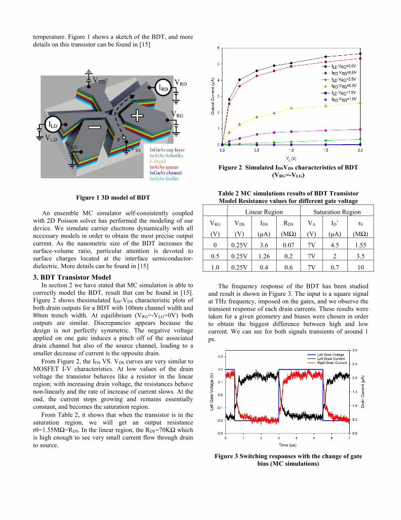
temperature. Figure 1 shows a sketch of the BDT, and more details on this transistor can be found in [15]
Figure 1 3D model of BDT An ensemble MC simulator self-consistently coupled
with 2D Poisson solver has performed the modeling of our device. We simulate carrier electrons dynamically with all necessary models in order to obtain the most precise output current. As the nanometric size of the BDT increases the surface-volume ratio, particular attention is devoted to surface charges located at the interface semiconductor-dielectric. More details can be found in [15]
3. BDT Transistor Model In section 2 we have stated that MC simulation is able to correctly model the BDT, result that can be found in [15]. Figure 2 shows thesimulated IDS-VDS characteristic plots of both drain outputs for a BDT with 100nm channel width and 80nm trench width. At equilibrium (VRG=-VLG=0V) both outputs are similar. Discrepancies appears because the design is not perfectly symmetric. The negative voltage applied on one gate induces a pinch off of the associated drain channel but also of the source channel, leading to a smaller decrease of current is the opposite drain. From Figure 2, the IDS VS. VDS curves are very similar to MOSFET I-V characteristics. At low values of the drain voltage the transistor behaves like a resistor in the linear region; with increasing drain voltage, the resistances behave non-linearly and the rate of increase of current slows. At the end, the current stops growing and remains essentially constant, and becomes the saturation region. From Table 2, it shows that when the transistor is in the saturation region, we will get an output resistance r0=1.55MΩ=RDS. In the linear region, the RDS=70KΩ which is high enough to see very small current flow through drain to source.
Figure 2 Simulated IDSVDS characteristics of BDT
(VRG=-VLG)
Table 2 MC simulations results of BDT Transistor Model Resistance values for different gate voltage
Linear Region Saturation Region
VRG
(V)
VDS
(V)
IDS
(μA)
RDS
(MΩ)
VA
(V)
ID’
(μA)
r0
(MΩ)
0 0.25V 3.6 0.07 7V 4.5 1.55
0.5 0.25V 1.26 0.2 7V 2 3.5
1.0 0.25V 0.4 0.6 7V 0.7 10
The frequency response of the BDT has been studied and result is shown in Figure 3. The input is a square signal at THz frequency, imposed on the gates, and we observe the transient response of each drain currents. These results were taken for a given geometry and biases were chosen in order to obtain the biggest difference between high and low current. We can see for both signals transients of around 1 ps.
Figure 3 Switching responses with the change of gate bias (MC simulations)

In Figure 3, we are able to extract the data for calculating the internal capacitance of the BDT. With a transient time of 1ps, the frequency response is 1THz.
, (1)
In equation (1), CGD and CGS are the gate to drain and gate to source capacitance, IRD is the right drain current. From Figure 3, we are able to get the change of the left gate voltage VLG in 0.3ps is 0.4V, the change of the right drain current is 1.5μA, then the CGD,GS=1.125aF.
Figure 4 Simple transistor model of BDT
Figure 4 presents the simple transistor model of BDT with AC analysis. D1 and D2 represent the left drain and right drain. G1 is the left gate, and G2 is the right gate. As the structure itself is symmetrical, we get Cg1d1=Cg1s=Cg2d2=Cg2s=1aF, Rd1s=Rd2s=1MΩ. The gm is in the range of 30μS to 200μS [14], depending on the different channel width of the BDT.
4. THz BDT Amplifier Design
Figure 5 A single-stage BDT amplifier
To compensate for the small gm of BDT devices, it is
critical to achieve high resonance Q at both inputs and outputs of the amplifier. Figure 5 shows a single-stage amplifier using BDT transistor. It is driving an RC load that is typical in on chip applications. Considering TL1, TL2, TL3 and TL4 are ideal THz transmission lines matched to 50Ω, by implementing the transistor model from Figure 4, we are able to build and simulate the circuits in ADS simulator.
In Figure 6 (a) for a single BDT amplifier with a gm of 200μA/V, there is only a loss; in Figure 6 (b) by connecting 48 BDTs in parallel, we come close to achieving a necessary gain. But they show a great potential as a broadband device. In order to obtain a higher gain, more BDTs can be added in parallel. As the footprint of the BDT is 1μm×1μm, the size allows us to add more. Although we are not able to analyze
the nonlinearity of the amplifier, it is believed that because of the inherent linearity of ballistic transport, it will be better than CMOS or HEMT.
Figure 6 (a) Power gain of the single BDT amplifier
Figure 6 (b) Power gain of 48 BDTs in parallel
In order to achieve larger output power, power
combining is very important. The best option is to apply the Travelling-Wave-Amplifier (TWA) structure, in which output signals from multiple devices are synchronously combined on the single output transmission line. In addition to higher output power, a TWA circuit can achieve a larger bandwidth, because the input/output impedance is lowered to the characteristic impedance of the loaded transmission line.
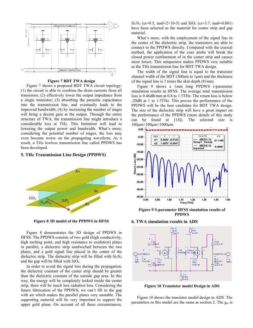
Figure 7 BDT TWA design Figure 7 shows a proposed BDT TWA circuit topology:
(1) the circuit is able to combine the drain currents from all transistors; (2) effectively lower the output impedance from a single transistor; (3) absorbing the parasitic capacitance into the transmission line, and eventually leads to the improved bandwidth; (4) by increasing the number of stages will bring a decent gain at the output. Through the entire structure of TWA, the transmission line might introduce a considerable loss at THz. This limitation will lead to lowering the output power and bandwidth. What’s more, considering the potential number of stages, the loss may even become worse on the propagating waveform. As a result, a THz lowloss transmission line called PPDWS has been developed.
5. THz Transmission Line Design (PPDWS)
Figure 8 3D model of the PPDWS in HFSS
Figure 8 demonstrates the 3D design of PPDWS in
HFSS. The PPDWS consists of two gold (high conductivity, high melting point, and high resistance to oxidation) plates in parallel, a dielectric strip sandwiched between the two plates, and a gold signal line placed in the center of the dielectric strip. The dielectric strip will be filled with Si3N4 and the gap will be filled with SiO2.
In order to avoid the signal loss during the propagation, the dielectric constant of the center strip should be greater than the dielectric constant of the outside gap area. In this way, the energy will be completely locked inside the center strip, there will be much less radiation loss. Considering the future fabrication of the PPDWS, we can’t fill in the gap with air which makes the parallel plates very unstable. The supporting material will be very important to support the upper gold plane. On account of all these circumstances,
Si3N4 (εr=9.5, tanδ=2×10⁻⁵) and SiO2 (εr=3.7, tanδ=0.001) have been selected as the material for center strip and gap material.
What’s more, with the employment of the signal line in the center of the dielectric strip, the transistors are able to connect to the PPDWS directly. Compared with the coaxial method, the application of the coax probe will break the closed power confinement of in the center strip and causes more losses. This uniqueness makes PPDWS very suitable as the THz transmission line for BDT TWA design.
The width of the signal line is equal to the transistor channel width of the BDT (300nm to 1μm) and the thickness of the signal line is 3 times the skin depth (81nm).
Figure 9 shows a 1mm long PPDWS s-parameter simulation results in HFSS. The average total transmission loss is 0.46dB/mm at 0.8 to 1.5THz. The return loss is below -20dB at 1 to 1.5THz. This proves the performance of the PPDWS will be the best candidate for BDT TWA design. The size of the dielectric strip will have a great impact on the performance of the PPDWS (more details of this study can be found at [14]). The selected size is 100μm×100μm×1000μm.
Figure 9 S-parameter HFSS simulation results of PPDWS
6. TWA simulation results in ADS
Figure 10 Transistor model Design in ADS
Figure 10 shows the transistor model design in ADS. The
parameters in this model are the same as section 2. The gm is

in the range of 30μS to 200μS. By importing the PPDWS design from HFSS we are able to build the following TWA structure presented in Figure 11.
Figure 11 24-stage TWA design with PPDWS Figure 11 shows the entire 24-stage TWA circuit design.
The drain lines and gate lines are composed of 25 segments of 20μm PPDWS. Between the drain lines and gate lines are the 24 stage of BDTs. Each stage consists of 48BDTs in parallel. As PPDWS has already been matched to 50Ω, we have the load impedance of 50Ω on both ends. It has a footprint around 524μm×48μm. Figure 12(a) shows the power gain simulation results of a gm=30μS, Figure 12 (b) shows the power gain simulation results of a gm=200μS.
Figure 12 (a) 24-stage gain with gm=30μS
Figure 12 (b) 24-stage gain with gm=200μS
We are not able to get enough gain out with smaller gm=30μS, but with a larger gm=200μS, we are able to obtain a 16.8dB power gain at 1.5THz, and the average gain at 1-2THz will be more than 10dB. Thanks to the small size of and low internal capacitance of BDTs, we are able to increase the number of stages to compensate for the low gm.
Figure 13 (a) shows the simulation results of a 48-stage TWA with a gm=30μS, Figure 13 (b) shows the simulation results of a 48-stage TWA with a gm=200μS. Here we find a 6dB gain increase for both conditions. Even with a low gm
we are still able to get decent gain about 6dB at 1.5THz; with a higher gm we are able to achieve result of 22.5dB gain at 1.5THz, and the average will be more than 15dB at 1-2THz. The footprint for a 48-stage TWA is 1028μm×48μm, which is still very small and has the potential to increase the number of stages to increase the gain. The simulation results verify the potential of the BDT TWA system and we are able to achieve much higher gain than we predicted in section 1.
Figure 13 (a) 48-stage gain with gm=30μS
Figure 13 (b) 48-stage gain with gm=200μS
7. Conclusion In conclusion a novel TWA design using the BDTs is
developed to be operated at more than 1THz, because of the

high operating frequency and high speed of BDT. We presented a lowloss THz transmission line we developed called the PPDWS to be used in the THz BDT TWA design. With its excellent performance, a low 0.46dB/mm transmission loss at 0.8-1.5THz, we are able to use the PPDWS to solve the power loss during the signal propagating in THz. We built the entire BDT TWA system in ADS, with imported PPDWS from HFSS, achieving a gain of 6dB at 1.5THz for gm=30μS, and a gain of 22.5dB at 1.5THz for gm=200μS. These results show a promising future for BDTs to be used to construct a traveling wave amplifier in the THz region. For this project we only focus on the performance of the amplifier, the cost is not considered in our project.
8. References
[1] Yan, Guofeng. et al., “Resonant THz sensor for paper
quality monitoring using THz fiber Bragg gratings.” Optics Letters, vol. 38, no. 13, 2013, pp. 2200–2202.
[2] J. F. Federici et al., “THz imaging and sensing for security applications-explosives, weapons and drugs,” Semicond. Sci. & Tech., no.20, S266-S280, 2005.
[3] X. Yang et al., “Biomedical Applications of Terahertz Spectroscopy and Imaging,” Trends in Biotech., vol.34, no.10, Oct. 2016
[4] I. F. Akyildiz et al., “Terahertz band: Next Frontier for wireless communications,” Physical Communication 12 (2014) 16-32
[5] K. Eriksson, V. Vassilev and H. Zirath, "H-band MMIC amplifiers in 250 nm InP DHBT," 2012 19th International Conference on Microwaves, Radar & Wireless Communications, Warsaw, 2012, pp. 744-747.
[6] A. Tessmann, A. Leuther, H. Massler, M. Kuri and R. Loesch, "A Metamorphic 220-320 GHz HEMT Amplifier MMIC," 2008 IEEE Compound Semiconductor Integrated Circuits Symposium, Monterey, CA, 2008, pp. 1-4.
[7] J. B. Hacker, Y. M. Lee, H. J. Park, J. S. Rieh and M. Kim, "A 325 GHz InP HBT Differential-Mode Amplifier," in IEEE Microwave and Wireless Components Letters, vol. 21, no. 5, pp. 264-266, May 2011
[8] H. Matsumura et al., "250–290 GHz amplifier in 75-nm InP HEMT technology using inverted microstrip transmission line," 2013 International Conference on Indium Phosphide and Related Materials (IPRM), Kobe, 2013, pp. 1-2.
[9] M. Schlechtweg et al., "Millimeter-wave circuits and modules up to 500 GHz based on metamorphic HEMT technology for remote sensing and wireless communication applications," 2011 IEEE 9th International New Circuits and systems conference, Bordeaux, 2011, pp. 269-272.
[10] W. R. Deal et al., "Scaling of InP HEMT Cascode Integrated Circuits to THz Frequencies," 2010 IEEE Compound Semiconductor Integrated Circuit Symposium (CSICS), Monterey, CA, 2010, pp. 1-4.
[11] J. Hacker, M. Urteaga, M. Seo, A. Skalare and R. Lin, "InP HBT amplifier MMICs operating to 0.67 THz," 2013 IEEE MTT-S International Microwave Symposium Digest (MTT), Seattle, WA, 2013, pp. 1-3.
[12] W. R. Deal, K. Leong, A. Zamora, V. Radisic and X. B. Mei, "Recent progress in scaling InP HEMT TMIC technology to 850 GHz," 2014 IEEE MTT-S International Microwave Symposium (IMS2014), Tampa, FL, 2014, pp. 1-3.
[13] V. Kaushal et al. “A Study of Geometry Effects on the Performance of Ballistic Deflection Transistor.” IEEE Transactions on Nanotechnology, vol. 9, no. 6, 2010, pp. 723–733.
[14] H. Wang, et al. “A Design of Terahertz Parrallel Plate Dielectric Waveguide with Signal line inserted for Ballistic Deflection Transistor Travelling Wave Amplifier.” Journal of Physics: Conference Series, Vol.906 012024, 2017.
[15] J. F. Milithaler, et al. “Study of surface charges in ballistic deflection transistors.” Nanotechnology, 2015 Dec 4;26(48):485202.