Embed Size (px)
Citation preview

Temperature-Dependent Thermal Boundary Conductance ofMonolayer MoS2 by Raman ThermometryEilam Yalon,† Ozgur Burak Aslan,‡,∇ Kirby K. H. Smithe,† Connor J. McClellan,†
Saurabh V. Suryavanshi,† Feng Xiong,†,○ Aditya Sood,§,∥ Christopher M. Neumann,† Xiaoqing Xu,⊥
Kenneth E. Goodson,§ Tony F. Heinz,‡,∇ and Eric Pop*,†,∥,#
†Department of Electrical Engineering, ‡Department of Applied Physics, §Department of Mechanical Engineering, ∥Department ofMaterials Science & Engineering, ⊥Stanford Nanofabrication Facility, and #Precourt Institute for Energy, Stanford University,Stanford, California 94305, United States∇SLAC National Accelerator Laboratory, Menlo Park, California 94025, United States
*S Supporting Information
ABSTRACT: The electrical and thermal behavior of nano-scale devices based on two-dimensional (2D) materials is oftenlimited by their contacts and interfaces. Here we report thetemperature-dependent thermal boundary conductance(TBC) of monolayer MoS2 with AlN and SiO2, usingRaman thermometry with laser-induced heating. The temper-ature-dependent optical absorption of the 2D material iscrucial in such experiments, which we characterize here for thefirst time above room temperature. We obtain TBC ∼ 15 MWm−2 K−1 near room temperature, increasing as ∼ T0.65 in the range 300−600 K. The similar TBC of MoS2 with the two substratesindicates that MoS2 is the “softer” material with weaker phonon irradiance, and the relatively low TBC signifies that suchinterfaces present a key bottleneck in energy dissipation from 2D devices. Our approach is needed to correctly perform Ramanthermometry of 2D materials, and our findings are key for understanding energy coupling at the nanoscale.
KEYWORDS: thermal boundary conductance (TBC), 2D materials, MoS2, Raman thermometry, optical absorption,aluminum nitride (AlN), Kapitza length
■ INTRODUCTION
Thermal interfaces are expected to dominate energy dissipationin 2D semiconductor devices, and their characterization andunderstanding have become essential.1,2 For example, drivecurrents in state-of-the-art 2D devices are critically limited bytheir heat dissipation capabilities,3,4 which are determined bythermal interfaces.1 Moreover, understanding the fundamentalsof heat flow across interfaces, namely, the thermal boundaryconductance (TBC), is an ongoing challenge in the thermalphysics of materials and calls for advances in existingexperimental techniques.5,6
Among existing techniques, Raman thermometry is attractiveto study 2D material thermal interfaces due to its materialselectivity. Raman thermometry enables unprecedented (nano-meter-scale) resolution along the laser path by simultaneouslymeasuring the temperature of several Raman-active materials,even monolayers like graphene and h-BN.7 Yet, characterizationof thermal properties requires not only a measurement of thetemperature but also an accurate definition of the input powerdensity and a suitable thermal model. With Ramanthermometry the temperature is measured optically, but theinput power could be either electrical1,7−9 or optical.10−14 TheJoule input power in electrical heating experiments is well-defined, but it requires fabricating high-quality devices that
carry high current densities sufficient to induce measurableJoule heating.1 These requirements limit the materials andstructures that can be used. The optical heating experiment,which simply requires increasing the Raman laser powerapplied to the sample, can readily be carried out on differentmaterials and stacks. Nevertheless, a challenge of the Ramanoptical heating experiment is to accurately define the relevantinput power and its density. Moreover, it is crucial tounderstand the heat dissipation mechanism in such experi-ments, as discussed below.We previously measured the TBC of monolayer (1L) MoS2
transistors on SiO2 by Raman thermometry with directelectrical self-heating (during transistor operation), finding G= 14 ± 4 MW m−2 K−1 near room temperature in exfoliatedand chemical vapor deposited (CVD) films.1 Recently, Yasaei etal.15 measured a larger value of G = 26 ± 7 MW m−2 K−1,however, by indirect heating across the MoS2 from a Ti/Auheater on top. These values are within reasonable agreement,given the uncertainties of the measurements. Our previouslymeasured TBC is equivalent to a Kapitza length LK ∼ 90 nm of
Received: August 4, 2017Accepted: October 20, 2017Published: October 20, 2017
Research Article
www.acsami.orgCite This: ACS Appl. Mater. Interfaces 2017, 9, 43013−43020
© 2017 American Chemical Society 43013 DOI: 10.1021/acsami.7b11641ACS Appl. Mater. Interfaces 2017, 9, 43013−43020

SiO2 (where kSiO2≈ 1.4 W m−1 K−1) at room temperature,
often dominating the thermal resistance of MoS2 devices.Here we measure the TBC of monolayer CVD-grown MoS2
on both SiO2 and AlN via direct optical heating, as a function oftemperature. Both interfaces (MoS2−SiO2 and MoS2−AlN)show very similar values of TBC (∼15 MW m−2 K−1), inagreement with our electrical heating experiments.1 MoS2−AlN−Si test structures highlight the unique material selectivityof the Raman technique, allowing us to simultaneously measurethe temperature of all three materials in the stack. In addition,the MoS2−SiO2 TBC is found to increase as Tn (n ∼ 0.65) inthe range from 25 to 300 °C. This finding is not unexpecteddue to the (positive) temperature dependence of the phononspecific heat, but it is in contrast with a previous study thatneglected the temperature dependence of the absorption.11
Here we take into account the T-dependent absorption of theMoS2, reporting it for the first time above room temperature.We also present a thermal model of the laser heatingexperiment for supported MoS2, emphasizing that the measure-ment is sensitive to the TBC but not to the thermalconductivity of the 2D film (k2D) when the lateral thermal
healing length is small compared to the laser spot size. Ourfindings provide important insights to understand heat transferacross 2D material interfaces, with implications for all optical,electronic, and thermoelectric devices based on such nanoma-terials.
■ RESULTS AND DISCUSSION
Raman and Temperature Calibration. Figure 1 showsthe measured MoS2 films, their Raman spectra, and temper-ature calibrations. MoS2 films were directly grown by CVD16
(see Methods) onto thin SiO2 (Figure 1a) and AlN17 (Figure1b) films on Si substrates. (To the best of our knowledge, thisalso represents the first demonstration of MoS2 grown by CVDdirectly onto AlN.) Section 1 of the Supporting Informationincludes TBC measurements of exfoliated 1L MoS2 showingsimilar results. The optical images in Figure 1a,b show large 1Ltriangular crystals (∼50 μm on SiO2 and ∼30 μm on AlN) withsmall (∼0.5 μm) bilayer regions.18 All Raman measurementswere carried out on the 1L MoS2 areas, as verified by theirRaman spectra (see ref 1).
Figure 1. Monolayer MoS2 Raman and temperature calibration. Optical image of CVD-grown MoS2 on (a) SiO2(94 nm)−Si and (b) on AlN(185nm)−Si showing large triangular crystals and small bilayer spots (∼0.5 μm in size). The measurements were carried out only on the 1L MoS2. (c) T-dependent Raman spectra at varying stage temperatures of the 1L MoS2 on SiO2(94 nm)−Si. (d) Simultaneous Raman spectra of MoS2 on AlN(185nm) on Si(substrate). The inset shows the AlN peaks, which have a weaker Raman signal compared with the Si and MoS2. Raman shift vs stagetemperature calibration of (e) MoS2 A1′ peak, (f) the Si substrate peak, and (g) AlN E2
2 peak. The absorbed laser power was kept below 20 μW in theMoS2 to avoid measurable laser heating during the calibration.
Figure 2. Laser heating experiment and thermal model. (a) Schematic sample structure and measurement setup. The thermal boundary resistance(=1/TBC) at the MoS2−SiO2 interface is highlighted. (b) Simulated temperature rise during laser heating in the 2D axisymmetric finite elementmodel. (c) Normalized power density and temperature rise in the MoS2 film vs radial coordinate for G = 15 MW m−2 K−1 and thermal conductivityk2D = 100 W m−1 K−1 illustrating a small thermal healing length (LH ∼ 80 nm) compared to the laser beam size (r0 ∼ 300 nm). The short LH resultsin the insensitivity of the measurement to the thermal conductivity of the 2D material (see Supporting Information, section 2).
ACS Applied Materials & Interfaces Research Article
DOI: 10.1021/acsami.7b11641ACS Appl. Mater. Interfaces 2017, 9, 43013−43020
43014

The Raman spectra of MoS2 on SiO2 vs stage temperatureare shown in Figure 1c, and the spectrum of MoS2 on AlN atroom T is shown in Figure 1d. The temperature calibration ofpeak shift vs stage temperature for MoS2 A1′, Si longitudinaloptical (LO), and AlN E2
2 modes, which served asthermometers, are shown in Figure 1e−g. For our AlN film,the weaker E2
2 mode is chosen as thermometer, due to its largermeasured temperature coefficient (χ = 0.022 cm−1/°C, wherethe mode frequency dependence is ω(T) = ω0 + χT) comparedwith the A1(TO) mode (χ < 0.01 cm−1/°C). The laser intensitywas kept low (Pabs < 20 μW) during the calibration to avoidmeasurable heating by the laser.Laser Heating. To better understand the heat dissipation in
our experiment, we model the laser heating (schematic shownin Figure 2a) using a finite element thermal simulation (withCOMSOL Multiphysics). The Fourier heat diffusion equationis solved with cylindrical coordinates (2D axisymmetricconfiguration) and a Gaussian-shaped beam heat source. Thesimulated temperature rise in the sample is shown in Figure 2b.The bottom of the substrate is held at ambient temperature(isothermal boundary condition) and other surface boundariesare thermally insulating (adiabatic boundary condition). Thethermal properties of the substrate are well-known, includingtheir temperature dependence around room temperature. Thethermal conductivity of doped silicon can be expressed as kSi ≈3 × 10⁴/T W m−1 K−1, the thermal conductivity of SiO2 is kSiO2
≈ ln(T0.52) − 1.6 W m−1 K−1 (where T is in Kelvin), and theTBC between the two is GSi−SiO2
≈ 600 MW m−2 K−1
(following refs 1, 19−23). The heating profile is proportionalto the laser spot size and the heat is dissipated mostly in thecross-plane direction into the Si substrate, typical for supportedfilms as discussed below.The Raman laser heating technique was originally developed
for bulk materials, where the thermal conductivity could beextracted,24 and was later extended to suspended 2D films.10,25
In suspended structures, the heat flows radially “in-plane” fromthe laser spot toward the supported part of the film, where theheat is sunk “cross-plane” (into the substrate). Thiscombination of in-plane and cross-plane heat flow enablesextracting both the thermal conductivity of the 2D film (k2D)and the TBC with the supporting substrate. The separationbetween the two unknown parameters is obtained by varyingthe laser spot size.10 By contrast, in supported 2D films, typicallythe lateral thermal healing length is small compared with thelaser spot size (see below); thus, the heat flows predominatelyin the cross-plane direction into the substrate and is thereforeprimarily sensitive to the TBC of the 2D film with the substrate.The heat dissipation mechanism can be understood by
comparing the heated area (laser spot) with the lateral thermalhealing length LH = (k2Dt2D/g )
1/2 (see, e.g., ref 26), where k2Dand t2D are the thermal conductivity and thickness of the 2Dfilm, respectively, and g is the total thermal conductance to thesubstrate per unit area. LH quantifies the characteristic lengthscale over which the heat travels laterally before sinking to thesubstrate and is on the order of ∼80 nm for 1L MoS2 onSiO2(94 nm)−Si (assuming k2D ∼ 100 W m−1 K−1,11,12,27 t2D =0.615 nm, g = 5 MW m−2 K−1), much shorter than the laserspot (r0 > ∼300 nm). This is illustrated in Figure 2c, whichcompares the simulated input power and the temperatureprofile in the MoS2. Section 2 of the Supporting Informationshows a similar comparison for different values of TBC and k2D.We therefore set k2D = 50 W m−1 K−1 in our thermal model12,27
and validated that the extracted TBC values were insensitive(within measurement uncertainty) to changes of k2D in therange 20−120 W m−1 K−1. Given these inputs to the finiteelement thermal model, the MoS2−SiO2 TBC remains a singlefitting parameter.We note that the laser spot size dominates the uncertainty of
the measurement and it is useful to vary the spot size during theheating experiment by sweeping the z-position of the objectivein order to reduce that uncertainty (∼10% in spot radius,equivalent to ∼20% in spot area; see the SupportingInformation, section 3). The uncertainty in spot size iscomparable to the LH, further signifying the insensitivity ofthe measurement to the in-plane thermal conductivity.
Absorbed Laser Power. The temperature in our experi-ment is measured by converting the Raman peak shifts duringlaser heating to temperature, using the calibrations shown inFigure 1. In addition to the temperature measurement, theextraction of TBC requires the characterization of absorbedlaser power in the supported MoS2 film, including itstemperature dependence. The absorbed power is obtainedhere by multiplying the incident laser power by the absorptionof a free-standing 1L MoS2 and by the enhancement factor ofthe substrate, as discussed below. We note that the opticalabsorption of MoS2 as a function of temperature is measuredand reported here for the first time over the 25−300 °Ctemperature range.Due to the strong interferences of multiple light reflections in
the 1L MoS2−SiO2−Si structure, it is difficult to directlymeasure the absorption of the supported film. We thereforeestimate the absorption of our 1L MoS2 on SiO2−Si bymultiplying the free-standing 1L MoS2 absorption by awavelength-dependent factor, the intensity of the electric field(of the electromagnetic wave of the laser) at the top surface ofSiO2−Si substrate relative to the intensity of the incident electricfield (namely, the enhancement factor of the SiO2−Si stack).The free-standing absorption is obtained by measuring the (T-dependent) absorption of 1L MoS2 on quartz, where the quartzdielectric function is known (see Methods). The enhancementfactor is calculated by the transfer matrix method28 using therefractive indices of the materials in the stack, which are knownat room temperature, and we assume that these reflections donot change significantly with T.Figure 3a displays four selected absorption spectra at selected
stage temperatures between 25 and 300 °C. Both A and Bexcitons red-shift from ∼1.82 and 1.97 eV to ∼1.75 and 1.88eV, respectively. Such red-shifts with increasing temperature aretypically found due to reduced overlap in the orbitals formingthe bands in the thermally expanded crystals. Figure 3a alsoshows that the absorption changes significantly near the A andB excitons. The 1L MoS2 absorption is obtained by averagingover two measured samples at commonly used laser wave-lengths of 488, 515, 532, and 633 nm and fitting them to alinear function of T (dashed lines in Figure 3b). It is evidentthat in green lasers, for instance, the absorption at 250 °C isincreased by ∼30% compared with its room temperature value.Overlooking this ∼30% increase in the absorbed power canresult in an underestimation of the TBC (and thermalconductivity in suspended films) of the 2D material inRaman thermometry experiments. These temperature-depend-ent absorption results are essential for calculating the absorbedlaser power of 1L MoS2 for Raman thermometry or otheroptoelectronic applications above room temperature.
ACS Applied Materials & Interfaces Research Article
DOI: 10.1021/acsami.7b11641ACS Appl. Mater. Interfaces 2017, 9, 43013−43020
43015

Figure 3c shows the calculated enhancement factor of theSiO2 (with thickness tox) on Si substrate, and Figure 3d showsthe absorption spectra of 1L MoS2 and the Si substrate, as wellas the reflected light of the MoS2−SiO2(94 nm)−Si stack. Mostof the laser power is absorbed in the Si substrate (within anabsorption depth, here ∼0.65 μm at wavelength λ = 532 nm),heating it above the ambient temperature in spite of itsrelatively large thermal conductivity (see the SupportingInformation, section 4).Thermal Boundary Conductance and Its Temperature
Dependence. Figure 4 summarizes the results of themeasured TBC of 1L MoS2 with SiO2 and AlN. Thetemperature rise vs absorbed power in the MoS2 on SiO2(thickness tox) on Si, with tox = 31 nm (blue) and 94 nm (red),is shown in Figure 4a. The laser spot size (r0) is characterized insection 3 of the Supporting Information, and the absorbedpower is calculated as described in Figure 3. The error bars inmeasured temperatures are from the uncertainty in Ramanmeasurement and peak fitting, and the error bars of absorbedpower are obtained by propagating error from uncertainty inthe three factors mentioned earlier: incident laser power,absorption, and enhancement factor.The temperature measured by Raman thermometry is
defined as follows10
∫∫
=
∞ −
∞ −T
T r r r
r r
( ) e d
e d
r r
r rm0
/
0/
20
2
20
2
(1)
where r0 is the beam radius. The TBC acts as a single fittingparameter in the thermal model discussed earlier and it isextracted for each measured temperature, given the inputpower and spot size (for details on the measured beam radius,see the Supporting Information, section 3).
The extracted TBCs are presented in Figure 4b for differentMoS2 temperatures. The stage temperature varied between 25and 200 °C. The results in Figure 4b include samples with andwithout a thin AlOx capping layer (see Methods), showing nomeasurable difference. The error bars of the TBC are obtainedfrom the uncertainty in the measured thermal resistance, whichis a function of the measured temperature, calculated absorbedpower, and the measured spot size. The MoS2−SiO2 interfaceaccounts for more than 50% of the thermal resistance of theMoS2−SiO2(94 nm)−Si stack, and more than 70% for the stackwith 31 nm SiO2. The magnitude and uncertainties of the Si−SiO2 interface thermal properties19,21,23 are small comparedwith the error bars in our measurement. The MoS2−SiO2 TBCshows a weak increase with temperature over the measuredrange, from 25 to 300 °C. The black dashed line is given by G =0.37T0.65 (in MW m−2 K−1, with T in K), and the TBCincreases by ∼40% in the measured temperature range.We emphasize here the importance of measuring the
temperature-dependent absorption of the MoS2. Section 5 ofthe Supporting Information shows that the thermal resistancewith respect to the incident laser power increases withtemperature, which might lead one to conclude that the TBCdecreases with increasing temperature,11 a physically unlikelyresult, as we discuss below. The reason for this apparentincrease of the thermal resistance is the increase in absorptionof the optical power with temperature (for the 532 nm laser,Figure 3a,b). By taking this effect into account, we find that thethermal resistance with respect to the absorbed power shows aminor decrease with temperature, and hence, the TBC slightlyincreases with temperature, as shown in Figure 4b.The TBC typically follows the temperature dependence of
the specific heat, which at low temperatures (T ≪ ΘD, whereΘD is the lower Debye temperature of the two materials
Figure 3. Optical absorption of monolayer MoS2. (a) Absorption of free-standing 1L MoS2 vs laser energy at temperatures from 25 to 300 °C. Twotypical visible Raman laser lines are indicated by dashed black lines (532 and 633 nm), and the excitonic peaks are labeled. (b) The temperaturedependence of optical absorption in free-standing 1L MoS2 (markers) and linear fits (dashed lines) for typical Raman laser lines: 488, 515, 532, and633 nm. Note that the absorption can change by more than ∼30% between room temperature and ∼250 °C. (c) Colormap of the substrateenhancement factor, defined as the intensity of the electric field (on SiO2−Si substrate) relative to the intensity of the incident electric field for laserwavelengths in the range of 400−800 nm and varying SiO2 thickness in the range of 10−400 nm. (d) Calculated absorption spectra of 1L MoS2 onSiO2(94 nm)−Si (red) and the Si substrate (dark blue) and the fraction of the light reflected (gray). Dielectric functions used for the calculation inpart d are taken from ref 29. The absorbed laser power in a supported 2D film is calculated as Pabs = PinαfE, where Pin is the incident laser power, αf isthe absorption of the free-standing film, and E is the enhancement factor of the substrate.
ACS Applied Materials & Interfaces Research Article
DOI: 10.1021/acsami.7b11641ACS Appl. Mater. Interfaces 2017, 9, 43013−43020
43016
forming the interface) takes the form ∝Td/m, where d is thedimensionality of the material with phonon dispersion ω ∼ qm,q being the phonon wavevector (see ref 2). At hightemperatures (T > ΘD) the specific heat approaches a constant,and the TBC likewise is expected to saturate. Thus, atintermediate temperatures, in the transition between these tworegimes, the TBC can be expected to increase more weakly, as∝Tn (where 0 ≤ n < d/m).5,30 In the case of 2D materials, thegraphene−SiO2 TBC was studied in the range from 50 to 500K and showed an increase with T up to ∼300 K, where theTBC saturates.31,32 In light of the higher ΘD of graphene33,34
than MoS2 we expect that the TBC of MoS2−SiO2 should havea weak temperature dependence for intermediate temperaturesas well, which is what we observe experimentally (Figure 4b).We also examined the TBC of monolayer MoS2 with AlN, as
shown in Figure 4c,d. The crystalline AlN layer has ameasurable Raman signal, whose temperature dependence canbe calibrated, as shown in Figure 1d,g. The absorbed power inthe MoS2 is obtained as outlined earlier, with the relevantenhancement factor calculated for the AlN(185 nm)−Si stack(Supporting Information, section 6). The measured temper-atures of the MoS2 (red), AlN (blue), and Si (black) in theRaman laser heating experiment are shown in Figure 4c as afunction of the absorbed power in the MoS2 film.The differential temperature measurement of all three
materials in the stack allows us to estimate the MoS2−AlNTBC as well as the thermal conductivity of the AlN film. In thiscase, the MoS2−AlN TBC is obtained from the temperaturedifference across the interface and kAlN is obtained from theAlN temperature (see the note in next paragraph on the AlN-SiTBC). This emphasizes the exceptional capability of the Ramantechnique to measure thermal interfaces without prior knowl-
edge of the thermal properties of the materials in the stack,thanks to its material selectivity. The dashed lines in Figure 4crepresent the thermal resistance of MoS2 and AlN in the laserheating experiment calculated from the model presented inFigure 2, with TBC = 15 MW m−2 K−1 and kAlN = 60 W m−1
K−1 (averaged between 300 and 400 K) with a laser spot radiusof r0 = 200 nm (measured for the objective used in thisexperiment, magnification 100×, NA = 0.9). The simulatedtemperature profile along the z-axis when the absorbed powerin the MoS2 is Pabs,MoS2 = 480 μW is shown in Figure 4d.We note that the temperature rise in the Si is not due to the
absorbed power in the MoS2, but rather due to the powerabsorbed by Si itself (Pabs,Si = 6.2 mW) within its absorptiondepth of ∼0.65 μm at the 532 nm laser wavelength35 (gray areain Figure 4d). In the Si substrate, both the absorbed power(heating) and the Raman signal (measured ΔT) originate fromthe Si surface. The absorbed power decays exponentially withthe absorption depth, whereas the substrate is 500 μm thick.The uncertainty in the measured thermal conductivity of theAlN is relatively large, since its temperature rise is low relativeto the uncertainty in Raman temperature measurement. Yet themeasured thermal resistance is dominated by the MoS2−AlNTBC, and therefore, the uncertainty in the measured TBC iscomparable to the one measured in MoS2−SiO2, in spite of therelatively large error in the measured kAlN. The simulatedtemperature profile shown in Figure 4d is insensitive (<3%error) to the AlN−Si TBC (in the range TBC > 10 MW m−2
K−1), since the AlN is mostly heated by the Si substrate in thiscase.An important result presented in Figure 4 is that the
measured TBCs between monolayer, CVD-grown MoS2, andtwo different materials, (1) amorphous SiO2 and (2) crystalline
Figure 4. TBC of monolayer MoS2 and its temperature dependence. (a) Measured temperature rise of 1L MoS2 on 31 nm (blue) and 94 nm (red)SiO2 on Si substrate vs absorbed laser power. Calculated absorbed power takes into account the measured temperature-dependent absorption ofMoS2 (Figure 3a,b) and reflections from the substrate, given the exact oxide thicknesses (Figure 3c). Slope of the dashed lines is the thermalresistance of each sample. (b) Measured TBC vs MoS2 temperature, weakly increasing up to ∼600 K. The extracted MoS2−SiO2 TBC is 17 ± 5 MWm−2 K−1 (averaged between 300 and 400 K) and the dashed black line shows Tn dependence with n = 0.65. (c) Measured temperature rise of MoS2(red) on AlN (blue) and Si (black) as a function of the absorbed power in the MoS2. The temperature of each material in the stack is measuredindependently by its Raman signal. The temperature rise of the Si is due to the absorbed power in the Si (see Figure 3d and Supporting Information,section 4). (d) Simulated temperature rise (Gaussian weighted across laser spot size) in the sample along the z-axis, at an absorbed power of 480μW. The gray area represents the absorption depth of the highly doped Si substrate, where the Si temperature is measured (and where power isabsorbed). The extracted MoS2−AlN TBC is 15 ± 4 MW m−2 K−1 (averaged between 300 and 400 K) and the estimated thermal conductivity of theAlN film is kAlN = 60 ± 15 W m−1 K−1.
ACS Applied Materials & Interfaces Research Article
DOI: 10.1021/acsami.7b11641ACS Appl. Mater. Interfaces 2017, 9, 43013−43020
43017

AlN, are very similar. It is interesting to note that the TBCbetween 1L MoS2 and hBN also showed similar values (∼17MW m−2 K−1) in a recent study.36 Furthermore, the measuredTBC values of MoS2−SiO2 and MoS2−sapphire interfacesreported in ref 15 are within a comparable range. Thesefindings suggest that the TBC is dominated by the materialwith the weaker energy irradiance across the interface (hereMoS2), as was recently proposed in ref 5. The energy irradianceis proportional to the specific heat and (cross-plane) carriervelocity and is expected to be lower in MoS2 compared withhBN, AlN, and SiO2.
37−39 (We note that the top few nm of ourAlN film could be oxidized during MoS2 growth, formingAlOxNy at the interface with MoS2.)The lower value of the TBC obtained here and in ref 1 (by
direct optical or electrical heating of the MoS2) compared withthe TBC reported in ref 15 (the MoS2 being heated indirectly bya metal on top) could be due to an “internal thermalresistance”40−42 between high-frequency optical phonon (OP)modes and low-frequency modes. If the TBC is dominated bylow-frequency modes, the interfacial thermal transport has twomain contributions: (i) an internal thermal resistance betweenthe OP modes that are excited (electrically or optically) and thelow-frequency modes and (ii) an external thermal resistancebetween the low-frequency modes in the MoS2 and thesubstrate. An indirect heating experiment probes only the latter(external) contribution to the thermal resistance, while theresult obtained here, in a direct heating experiment, is therelevant one for devices where the power is dissipated withinthe MoS2 film or device.The Raman thermometry method with optical heating can
also be applied, in principle, to multilayer (ML) films, if thetemperature-dependent absorption and Raman shifts of thespecific ML can be determined. We can also estimate theinternal TBC between individual layers of a bulk (or thick ML)film, by normalizing the cross-plane bulk thermal conductivityof MoS2 (∼2 W/m/K)43 by the layer thickness (∼0.615 nm).The internal TBC between MoS2 layers is thus ∼3 GW m−2
K−1, two orders of magnitude higher than the TBC with thesubstrate (for comparison, the interlayer thermal conductanceof bulk graphite2 is ∼18 GW m−2 K−1). In other words, theMoS2−SiO2 TBC is equivalent to ∼200 layers, or a Kapitzalength corresponding to ∼130 nm thick bulk MoS2. However,in thinner MoS2 films quasi-ballistic cross-plane transporteffects37 must be considered to properly account for theinterplay of the TBC and that of the internal thermal resistance,which could be the subject of future work.
■ CONCLUSIONSIn summary, we measured the temperature-dependent TBC of1L MoS2−SiO2, and the TBC of MoS2−AlN by Ramanthermometry with optical heating. We identified some criticalpoints in the analysis of the laser heating experiment: (1)understanding the heat dissipation that is dominated by cross-plane transport across the interface and (2) characterization ofthe absorbed power density, including measurement of the T-dependent absorption and measurement of the laser spot size atvarying offsets of the focal plane. Near room temperature, weobtain similar values of the 1L MoS2−SiO2 TBC as previouslymeasured by electrical heating, equivalent to a Kapitza length of∼90 nm SiO2. Knowledge of the T-dependent absorption α(T)is essential to extract the correct T-dependent thermalproperties in such optical heating experiments. Taking intoaccount the measured α(T), we find that the TBC weakly
increases with temperature in the range 25−300 °C, in contrastto a previous study.11
We characterized the TBC of MoS2−AlN by leveraging thesimultaneous temperature measurement of all three materials inthe stack (MoS2−AlN−Si), as uniquely enabled by the Ramantechnique. The obtained MoS2−AlN TBC is similar to that ofthe 1L MoS2−SiO2 measured here and 1L MoS2−hBNmeasured in an earlier study,36 suggesting that the TBC ofthese interfaces is limited by the MoS2, which has lower (cross-plane) Debye temperature and phonon irradiance. Our findingsare essential to interpret Raman thermometry experiments andto understand the heat dissipation in all optoelectronic devicesbased on 2D materials.
■ METHODSMaterial Growth. We study monolayer MoS2 grown by CVD on
SiO2 (tox = 31 or 94 nm), as well as AlN (185 nm), both on Sisubstrates (p+, electrical resistivity of 1−5 mΩ cm). A subset of theMoS2−SiO2(94 nm)−Si samples were capped by ∼15 nm AlOx, asdescribed in ref 1. More details can be found in ref 16. The 185 nmthick AlN was grown by MOCVD on the Si substrate immediatelyafter an HF dip to remove the native oxide. The dislocation density inthe AlN film is expected to be ∼109 cm−2 due to the lattice mismatchand polarity difference.17 The MoS2 was deposited by CVD at 850 °Cdirectly on the AlN, in a process similar to the one described in refs 16and 18.
Characterization. Raman spectroscopy was carried out using aHoriba LabRam Revolution HR instrument with a 532 nm laser, 1800l/mm grating, and two different objectives: a 100× long workingdistance (LWD) objective with numerical aperture NA = 0.6 and a100× objective with NA = 0.9. Temperature calibration was done witha Linkam THMS600 stage in ambient air. The peak position of eachRaman mode was fitted to a single Lorentzian line shape. Aftercalibrating Raman peak shifts vs temperature on a hot stage (Figure 1),we increase the applied laser power, and the MoS2 temperature wasmeasured by converting the Raman peak shifts (of MoS2, Si, and AlN)to temperature rise (the measured temperature is a weighted Gaussianacross the laser spot).10
The absorption of CVD-grown 1L MoS2 on a quartz substrate wasmeasured at temperatures from 25 up to 300 °C in the LinkamTHMS600 stage. We studied two samples for all temperatures andcalculated the absorption spectra of free-standing 1L MoS2 from thesemeasurements.44−46
■ ASSOCIATED CONTENT*S Supporting InformationThe Supporting Information is available free of charge on theACS Publications website at DOI: 10.1021/acsami.7b11641.
Sections detailing the TBC of exfoliated MoS2, thesensitivity of laser heating to thermal conductivity ofsupported 2D film, the laser spot, the heating byabsorbed power in Si substrate, the thermal resistanceof incident vs absorbed power, and the enhancementfactor of AlN−Si substrate (PDF)
■ AUTHOR INFORMATIONCorresponding Author*E-mail: [email protected] Yalon: 0000-0001-7965-459XKirby K. H. Smithe: 0000-0003-2810-295XConnor J. McClellan: 0000-0002-8733-9968Christopher M. Neumann: 0000-0002-4705-9478Eric Pop: 0000-0003-0436-8534
ACS Applied Materials & Interfaces Research Article
DOI: 10.1021/acsami.7b11641ACS Appl. Mater. Interfaces 2017, 9, 43013−43020
43018

Present Address○F.X.: Department of Electrical & Computer Engineering,University of Pittsburgh, Pittsburgh, PA 15261, USA.
NotesThe authors declare no competing financial interest.
■ ACKNOWLEDGMENTS
We thank Pawel Keblinski for fruitful discussions. Weacknowledge the Stanford Nanofabrication Facility (SNF)and Stanford Nano Shared Facilities (SNSF) for enablingdevice fabrication and measurements. This work was supportedin part by National Science Foundation (NSF) EFRI 2-DAREgrant 1542883, by the NSF Center for Power Optimization ofElectro-Thermal Systems (POETS) under grant EEC-1449548,by the NSF DMREF grant 1534279, by the Stanford SystemXAlliance, by NSF DMR-1411107 (O.B.A.), and by theDepartment of Energy, Office of Science, Basic EnergySciences, Materials Sciences and Engineering Division, underContract DE-AC02-76SF00515 (T. F. H.). E.Y. acknowledgespartial support from Ilan Ramon Fulbright Fellowship and fromthe Andrew and Erna Finci Viterbi Foundation. K.K.H.S.acknowledges partial support from the Stanford GraduateFellowship (SGF) program and NSF Graduate ResearchFellowship under Grant No. DGE-114747.
■ REFERENCES(1) Yalon, E.; McClellan, C. J.; Smithe, K. K.; Munoz Rojo, M.; Xu,R. L.; Suryavanshi, S. V.; Gabourie, A. J.; Neumann, C. M.; Xiong, F.;Farimani, A. B.; Pop, E. Energy Dissipation in Monolayer MoS2Electronics. Nano Lett. 2017, 17, 3429−3433.(2) Pop, E.; Varshney, V.; Roy, A. K. Thermal Properties ofGraphene: Fundamentals and Applications. MRS Bull. 2012, 37 (12),1273−1281.(3) Suryavanshi, S. V.; Pop, E. S2DS: Physics-Based Compact Modelfor Circuit Simulation of Two-Dimensional Semiconductor DevicesIncluding Non-Idealities. J. Appl. Phys. 2016, 120 (22), 224503.(4) McClellan, C. J.; Yalon, E.; Smithe, K. K. H.; Suryavanshi, S. V.;Pop, E. Effective N-Type Doping of Monolayer MoS2 by AlOx. IEEEDevice Research Conference (DRC) 2017 , DOI: 10.1109/DRC.2017.7999392.(5) Monachon, C.; Weber, L.; Dames, C. Thermal BoundaryConductance: A Materials Science Perspective. Annu. Rev. Mater. Res.2016, 46, 433−463.(6) Yue, Y.; Zhang, J.; Xie, Y.; Chen, W.; Wang, X. Energy CouplingAcross Low-Dimensional Contact Interfaces at The Atomic Scale. Int.J. Heat Mass Transfer 2017, 110, 827−844.(7) Chen, C.-C.; Li, Z.; Shi, L.; Cronin, S. B. Thermal interfaceconductance across a graphene/hexagonal boron nitride hetero-junction. Appl. Phys. Lett. 2014, 104 (8), 081908.(8) Freitag, M.; Steiner, M.; Martin, Y.; Perebeinos, V.; Chen, Z.;Tsang, J. C.; Avouris, P. Energy Dissipation in Graphene Field-EffectTransistors. Nano Lett. 2009, 9 (5), 1883−1888.(9) Yue, Y.; Zhang, J.; Wang, X. Micro/Nanoscale Spatial ResolutionTemperature Probing for the Interfacial Thermal Characterization ofEpitaxial Graphene on 4H - SiC. Small 2011, 7 (23), 3324−3333.(10) Cai, W.; Moore, A. L.; Zhu, Y.; Li, X.; Chen, S.; Shi, L.; Ruoff, R.S. Thermal Transport in Suspended and Supported MonolayerGraphene Grown by Chemical Vapor Deposition. Nano Lett. 2010,10 (5), 1645−1651.(11) Taube, A.; Judek, J.; Lapin ska, A.; Zdrojek, M. Temperature-Dependent Thermal Properties of Supported MoS2 Monolayers. ACSAppl. Mater. Interfaces 2015, 7 (9), 5061−5065.(12) Zhang, X.; Sun, D.; Li, Y.; Lee, G.-H.; Cui, X.; Chenet, D.; You,Y.; Heinz, T. F.; Hone, J. C. Measurement of Lateral and InterfacialThermal Conductivity of Single-and Bilayer MoS2 and MoSe2 Using
Refined Optothermal Raman Technique. ACS Appl. Mater. Interfaces2015, 7 (46), 25923−25929.(13) Judek, J.; Gertych, A. P.; Swiniarski, M.; Lapinska, A.; Duzynska,A.; Zdrojek, M. High Accuracy Determination of The ThermalProperties of Supported 2D Materials. Sci. Rep. 2015, 5, 12422.(14) Lin, Z.; Liu, C.; Chai, Y. High Thermally Conductive andElectrically Insulating 2D Boron Nitride Nanosheet for Efficient HeatDissipation of High-Power Transistors. 2D Mater. 2016, 3 (4),041009.(15) Yasaei, P.; Foss, C. J.; Karis, K.; Behranginia, A.; El-Ghandour,A. I.; Fathizadeh, A.; Olivares, J.; Majee, A. K.; Foster, C. D.; Khalili-Araghi, F.; Aksamija, Z.; Salehi-Khojin, A. Interfacial ThermalTransport in Monolayer MoS2- and Graphene-Based Devices. Adv.Mater. Interfaces 2017, 4, 1700334.(16) Smithe, K. K. H.; English, C. D.; Suryavanshi, S. V.; Pop, E.Intrinsic Electrical Transport and Performance Projections ofSynthetic Monolayer MoS2 Devices. 2D Mater. 2017, 4 (1), 011009.(17) Xu, X.; Zhong, J.; So, H.; Norvilas, A.; Sommerhalter, C.;Senesky, D. G.; Tang, M. Wafer-Level MOCVD Growth of AlGaN/GaN-on-Si HEMT Structures with Ultra-High Room Temperature2DEG Mobility. AIP Adv. 2016, 6 (11), 115016.(18) Smithe, K. K.; Suryavanshi, S. V.; Munoz Rojo, M.; Tedjarati, A.D.; Pop, E. Low Variability in Synthetic Monolayer MoS2 Devices.ACS Nano 2017, 11 (8), 8456−8463.(19) Chien, H.-C.; Yao, D.-J.; Huang, M.-J.; Chang, T.-Y. ThermalConductivity Measurement and Interface Thermal ResistanceEstimation Using SiO2 Thin Film. Rev. Sci. Instrum. 2008, 79 (5),054902.(20) Asheghi, M.; Kurabayashi, K.; Kasnavi, R.; Goodson, K. E.Thermal Conduction in Doped Single-Crystal Silicon Films. J. Appl.Phys. 2002, 91 (8), 5079−5088.(21) Dorgan, V. E.; Bae, M.-H.; Pop, E. Mobility and SaturationVelocity in Graphene on SiO2. Appl. Phys. Lett. 2010, 97 (8), 082112.(22) Lee, S.-M.; Cahill, D. G. Heat Transport in Thin DielectricFilms. J. Appl. Phys. 1997, 81 (6), 2590−2595.(23) Kimling, J.; Philippi-Kobs, A.; Jacobsohn, J.; Oepen, H. P.;Cahill, D. G. Thermal Conductance of Interfaces With AmorphousSiO2 Measured by Time-Resolved Magneto-Optic Kerr-EffectThermometry. Phys. Rev. B: Condens. Matter Mater. Phys. 2017, 95(18), 184305.(24) Perichon, S.; Lysenko, V.; Remaki, B.; Barbier, D.;Champagnon, B. Measurement of Porous Silicon Thermal Con-ductivity by Micro-Raman Scattering. J. Appl. Phys. 1999, 86 (8),4700−4702.(25) Balandin, A. A.; Ghosh, S.; Bao, W.; Calizo, I.; Teweldebrhan,D.; Miao, F.; Lau, C. N. Superior Thermal Conductivity of Single-Layer Graphene. Nano Lett. 2008, 8 (3), 902−907.(26) Pop, E. Energy Dissipation and Transport in Nanoscale Devices.Nano Res. 2010, 3 (3), 147−169.(27) Yan, R.; Simpson, J. R.; Bertolazzi, S.; Brivio, J.; Watson, M.;Wu, X.; Kis, A.; Luo, T.; Hight Walker, A. R.; Xing, H. G. ThermalConductivity of Monolayer Molybdenum Disulfide Obtained fromTemperature-Dependent Raman Spectroscopy. ACS Nano 2014, 8(1), 986−993.(28) Byrnes, S. J. Multilayer Optical Calculations. arXiv preprint,arXiv:1603.02720 [physics.comp-ph], 2016.(29) Li, Y.; Chernikov, A.; Zhang, X.; Rigosi, A.; Hill, H. M.; van derZande, A. M.; Chenet, D. A.; Shih, E.-M.; Hone, J.; Heinz, T. F.Measurement of The Optical Dielectric Function of MonolayerTransition-Metal Dichalcogenides: MoS2, MoSe2, WS2, and WSe2.Phys. Rev. B: Condens. Matter Mater. Phys. 2014, 90 (20), 205422.(30) Swartz, E. T.; Pohl, R. O. Thermal Boundary Resistance. Rev.Mod. Phys. 1989, 61 (3), 605.(31) Koh, Y. K.; Bae, M.-H.; Cahill, D. G.; Pop, E. Heat ConductionAcross Monolayer and Few-Layer Graphenes. Nano Lett. 2010, 10(11), 4363−4368.(32) Chen, Z.; Jang, W.; Bao, W.; Lau, C.; Dames, C. ThermalContact Resistance Between Graphene and Silicon Dioxide. Appl.Phys. Lett. 2009, 95 (16), 161910.
ACS Applied Materials & Interfaces Research Article
DOI: 10.1021/acsami.7b11641ACS Appl. Mater. Interfaces 2017, 9, 43013−43020
43019

(33) Komatsu, K. Theory of The Specific Heat of Graphite II. J. Phys.Soc. Jpn. 1955, 10 (5), 346−356.(34) Andersson, O. E.; Prasad, B.; Sato, H.; Enoki, T.; Hishiyama, Y.;Kaburagi, Y.; Yoshikawa, M.; Bandow, S. Structure and ElectronicProperties of Graphite Nanoparticles. Phys. Rev. B: Condens. MatterMater. Phys. 1998, 58 (24), 16387.(35) Jellison, G. E., Jr; Modine, F. A.; White, C. W.; Wood, R. F.;Young, R. T. Optical Properties of Heavily Doped Silicon Between 1.5and 4.1 eV. Phys. Rev. Lett. 1981, 46 (21), 1414.(36) Liu, Y.; Ong, Z.-Y.; Wu, J.; Zhao, Y.; Watanabe, K.; Taniguchi,T.; Chi, D.; Zhang, G.; Thong, J. T.; Qiu, C.-W.; Hippalgaonkar, K.Thermal Conductance of the 2D MoS2/h-BN and Graphene/h-BNInterfaces. Sci. Rep. 2017, 7, 43886.(37) Li, Z.; Liu, Y.; Lindsay, L.; Xu, Y.; Duan, W.; Pop, E., SizeDependence and Ballistic Limits of Thermal Transport in AnisotropicLayered Two-Dimensional Materials. preprint arXiv:1711.02772(2017).(38) Wakabayashi, N.; Smith, H.; Nicklow, R. Lattice Dynamics ofHexagonal MoS2 Studied by Neutron Scattering. Phys. Rev. B 1975, 12(2), 659.(39) Ho, C.; Wu, C.; Huang, Y.; Liao, P.; Tiong, K. TemperatureDependence of Energies and Broadening Parameters of The Band-Edge Excitons of Mo1−xWxS2 Single Crystals. J. Phys.: Condens. Matter1998, 10 (41), 9317.(40) Hu, L.; Desai, T.; Keblinski, P. Determination of InterfacialThermal Resistance at The Nanoscale. Phys. Rev. B: Condens. MatterMater. Phys. 2011, 83 (19), 195423.(41) Shen, M.; Schelling, P. K.; Keblinski, P. Heat TransferMechanism Across Few-Layer Graphene by Molecular Dynamics.Phys. Rev. B: Condens. Matter Mater. Phys. 2013, 88 (4), 045444.(42) Steiner, M.; Freitag, M.; Perebeinos, V.; Tsang, J. C.; Small, J. P.;Kinoshita, M.; Yuan, D.; Liu, J.; Avouris, P. Phonon Populations andElectrical Power Dissipation in Carbon Nanotube Transistors. Nat.Nanotechnol. 2009, 4 (5), 320−324.(43) Liu, J.; Choi, G.-M.; Cahill, D. G. Measurement of TheAnisotropic Thermal Conductivity of Molybdenum Disulfide by TheTime-Resolved Magneto-Optic Kerr Effect. J. Appl. Phys. 2014, 116(23), 233107.(44) Mak, K. F.; Sfeir, M. Y.; Wu, Y.; Lui, C. H.; Misewich, J. A.;Heinz, T. F. Measurement of The Optical Conductivity of Graphene.Phys. Rev. Lett. 2008, 101 (19), 196405.(45) McIntyre, J.; Aspnes, D. Differential Reflection Spectroscopy ofVery Thin Surface Films. Surf. Sci. 1971, 24 (2), 417−434.(46) Buckley, R.; Beaglehole, D. Absorptance of Thin Films. Appl.Opt. 1977, 16 (9), 2495−2499.
ACS Applied Materials & Interfaces Research Article
DOI: 10.1021/acsami.7b11641ACS Appl. Mater. Interfaces 2017, 9, 43013−43020
43020

Yalon et al. Supporting Information S-1
Supporting Information
Temperature Dependent Thermal Boundary Conductance of
Monolayer MoS2 by Raman Thermometry
Eilam Yalon1, Özgür Burak Aslan2, Kirby K. H. Smithe1, Connor J. McClellan1, Saurabh V. Surya-
vanshi1, Feng Xiong1,3, Aditya Sood4,5, Christopher M. Neumann1, Xiaoqing Xu6, Kenneth E.
Goodson4, Tony F. Heinz2, and Eric Pop1,5,7,*
1Department of Electrical Engineering, Stanford University, Stanford, CA 94305, USA. 2Depart-
ment of Applied Physics, Stanford University, Stanford, CA 94305, USA & SLAC National Accel-
erator Laboratory, Menlo Park, CA 94025, USA.3Present address: Department of Electrical &
Computer Engineering, University of Pittsburgh, Pittsburgh, PA 15261, USA. 4Department of Me-
chanical Engineering, Stanford University, Stanford, CA 94305, USA. 5Department of Materials
Science & Engineering, Stanford University, Stanford, CA 94305, USA. 6Stanford Nanofabrication
Facility, Stanford University, Stanford, CA 94305, USA. 7Precourt Institute for Energy, Stanford
University, Stanford, CA 94305, USA. *E-mail: [email protected]
Table of Contents
1. TBC of exfoliated MoS2
2. Sensitivity of laser heating to thermal conductivity of supported 2D film
3. Laser spot
4. Heating by absorbed power in Si substrate
5. Thermal resistance of incident vs. absorbed power
6. Enhancement factor of AlN-Si substrate

Yalon et al. Supporting Information S-2
1. TBC of exfoliated MoS2
Figure S1 compares the thermal boundary conductance (TBC) of monolayer (1L) MoS2-SiO2, pre-
pared by chemical vapor deposition (CVD, black) and exfoliation (red). Evidently, there is no
measurable difference between the CVD and exfoliated samples. We note that the CVD samples
were directly grown onto the SiO2-Si substrate (at 850 oC, see Ref. 1 ) while the exfoliated samples
were prepared at room temperature from bulk MoS2 on identical substrates. These results suggest
that any residual strain from the high-temperature growth of MoS2 has little, if any, effect on the
TBC of this material with SiO2.
Figure S1 | Temperature dependent thermal boundary conductance (TBC) of exfoliated (red)
and CVD-grown (black) 1L MoS2 with SiO2.
2. Sensitivity of laser heating to thermal conductivity of supported 2D film
Figure S2 shows the simulated temperature rise in 1L MoS2 on SiO2(90 nm)-Si vs. laser spot size,
for different values of TBC and in-plane MoS2 thermal conductivity (k2D). The figure illustrates
the (in)sensitivity of the laser heating experiment (with varying spot size) to the in-plane thermal
conductivity. It is evident that for TBC > ~ 5 MWm-2K-1 and spot sizes > ~ 300 nm, as in the
experiment discussed in the main text, the measurement is insensitive to the thermal conductivity
of a monolayer transition metal dichalcogenide (where k2D < ~ 100 Wm-1K-1),2-3 and therefore its
k2D cannot be reliably extracted. The k2D values shown in Figure S2 are chosen to be in the range
of those previously measured for 1L MoS2 (see e.g. Ref. 2) and are varied in the simulation by
more than an order of magnitude to examine the (in)sensitivity of our measurement to k2D.
For high thermal conductivity 2D materials such as graphene and hBN, where k2D is ~ 10 larger
compared with MoS2,4-8 the thermal healing length (see Results and Discussion Section in the main
text) could be ~ 3 longer (if the TBC is similar). In this case the sensitivity of the measurement
to k2D improves, but not significantly. A more reliable extraction of k2D requires that the thermal
healing length should be few times larger than the laser spot size, which can be obtained by sus-
pending the 2D film.
0 50 100 150 200 250 3000
10
20
30
T (C)
TB
C (
MW
m-2K
-1)
00
10
20
30
TB
C (
MW
m-2
K-1
)
50 100 150 200 250 300
T ( C)
CVD
exfoliated

Yalon et al. Supporting Information S-3
Figure S2 | Sensitivity of laser heating to thermal conductivity of supported 1L MoS2. Simu-
lated temperature rise in 1L MoS2 on SiO2(90 nm)-Si vs. spot radius with different values of TBC
= (a) 15 (b) 10 (c) 5 and (d) 1 MWm-2K-1 and thermal conductivity k2D = 10 (red), 50 (green), and
150 (blue) Wm-1K-1 of the MoS2. The absorbed laser power is normalized to induce ΔTmax = 100 °C
in each panel.
3. Laser spot
The Raman thermometry technique was historically extended from bulk samples9 to suspended
2D films,10 which required varying the spot size in order to extract two fitting parameters: the in-
plane thermal conductivity of the 2D film (k2D) and the thermal boundary conductance (TBC) at
the edges where the film is supported.11
Our measurement of fully-supported 2D films, however, is sensitive almost entirely to a single
parameter: the TBC (see Figure S2). It is therefore, in principle, possible to extract the TBC from
a single measurement. However, the laser spot size dominates the uncertainty of the measurement
and it is useful to vary the spot size during the heating experiment, e.g. by sweeping the z-position
of the objective.
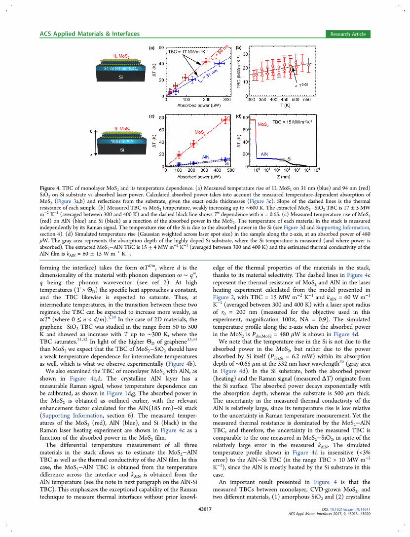
Figure S3 displays our characterization of the laser spot shape and size. We carry out the knife
edge experiment11-12 illustrated in Figure S3a, where the laser beam is scanned along the x-axis
across a sharp edge that blocks the Raman signal, such as a nearby metal film (> ~ 20 nm thick).
200 400 600 800 10000
20
40
60
80
100
Spot Radius (nm)
T
(K
)
TBC = 5 MWm-2K-1
TBC = 10 MWm-2K-1TBC = 15 MWm-2K-1
TBC = 1 MWm-2K-1
k2D=10 W/m/K
k2D=150 W/m/K
k2D=50 W/m/K
k2D=10 W/m/K
k2D=150 W/m/K
k2D=50 W/m/K
k2D=10 W/m/K
k2D=150 W/m/K
k2D=50 W/m/K
k2D=10 W/m/K
k2D=150 W/m/K
k2D=50 W/m/K
200 400 600 800
Spot radius (nm)
10000
20
40
60
ΔT
( C
)
100
0
ΔT
( C
)
200 400 600 800
Spot radius (nm)
1000
200 400 600 800
Spot radius (nm)
1000 200 400 600 800
Spot radius (nm)
1000
ΔT
( C
)
ΔT
( C
)
80
20
40
60
100
80
0
20
40
60
100
80
0
20
40
60
100
80
Yalon et al. Supporting Information S-4
The Gaussian shape of the laser intensity yields a decay of the integrated Raman signal area fol-
lowing the form of the complementary error function (erfc) as the laser is scanned across the
metal edge (Figure S3 b-c). The spot radius can be extracted by fitting an erfc to the measured
integrated area (Figure 3c). We repeat the knife edge method for varying offsets in the z-axis to
find the focal plane and the minimum spot size (shown in Figure S3b-c after correction to set r0
at z=0). We find that in a single measurement the spot size could vary due to small offsets in the
z-axis from the focal plane and we carry out the laser heating experiment at varying z-offsets to
reduce this uncertainty in our measurement. We note that r0 at the focal plane (z=0) is defined
here as in Ref. 11 via I exp(-r2/r02), where I is the Raman intensity. Our r0 = √2/3 srad ≈ 0.5srad,
where srad = 3σ of a Gaussian profile I exp(-r2/2σ2). The measured srad ≈ 600 nm and the dif-
fraction limited spot radius is 0.61λ/N.A = 540 nm.
The good agreement between the measured area and the fitted erfc shown in Figure S3c confirms
the Gaussian shape of the laser at varying offsets in the z-position. We extract the spot radius at
each z-position and plot the extracted spot radii vs. offset in z to find the minimum spot size as
shown in Figure S3d. We note that for each power input of the laser heating experiment we sweep
the z-offset to reduce the uncertainty in the laser spot size. The uncertainty in the laser spot size is
10% of the spot radius (shown in Figure S3d), resulting in 20% error in spot area. This uncertainty
in spot area is a leading factor in the uncertainty of the measured TBC (see main text). It is also
evident that the thermal healing length of 1L MoS2 on SiO2 (where G ~ 15 MWm-2K-1 and k2D <
~ 100 Wm-1K-1 following refs 2-3, 13) is comparable to the uncertainty in the spot size, further
signifying the insensitivity of the measurement to the in-plane thermal conductivity within that
range (k2D ~ 100 Wm-1K-1), as discussed above.
Figure S3 | Laser beam shape and spot size. (a) Schematic of the “knife edge” experiment12 with
varying spot size. The laser is scanned in the x-axis across a sharp edge of a metal that blocks the
-2 -1 0 1 20
0.2
0.4
0.6
0.8
1
1.2
z offset (m)
Spot
Radiu
s (
m)
x
z
-2 -1 0 1 20
0.2
0.4
0.6
0.8
1
x (m)
Are
a (
a.u
.)
22 2
0r = r +a z
r0=300 30 nm
A erfc(x/r(z))
|z|
|z|
2r0
X (µm) Z offset (µm)
-2 -1 0 1 2
Sp
ot
rad
ius (
µm
)
0
0.2
0.4
0.6
0.8
1
1.2
-2 -1 0 1 2
Are
a (
a.u
.)
0
0.2
0.4
0.6
0.8
1
X (µm)
-2 -1 0 1 2-2
-1
0
1
2
Z o
ffse
t (µ
m)
1
0.2
0.4
0.6
0.8
metal1L MoS2
SiO2
Si
Yalon et al. Supporting Information S-5
Raman signal. The spot size is varied by defocusing the laser spot (offset in the z-axis). (b) x-z
map of the MoS2 integrated Raman signal intensity (normalized). White dashed line is a guide to
the eye representing the bounds (horizontal axis) of the spot size for each z-offset. (c) The meas-
ured integrated area vs. position along the x-axis and fit to complementary error function (erfc) for
different offsets from the focal plane in z (same data as in b). (d) Extracted spot radii (blue symbols)
from the erfc fits shown in (c) as a function of the offset in z. Dashed black line is a fit to the spot
radius dependence on z, with extracted minimum radius r0 = 300 ± 30 nm. The parameter a = 0.48
± 0.02 extracted by the fit in (d) is proportional to the N.A (=0.6) of the objective.
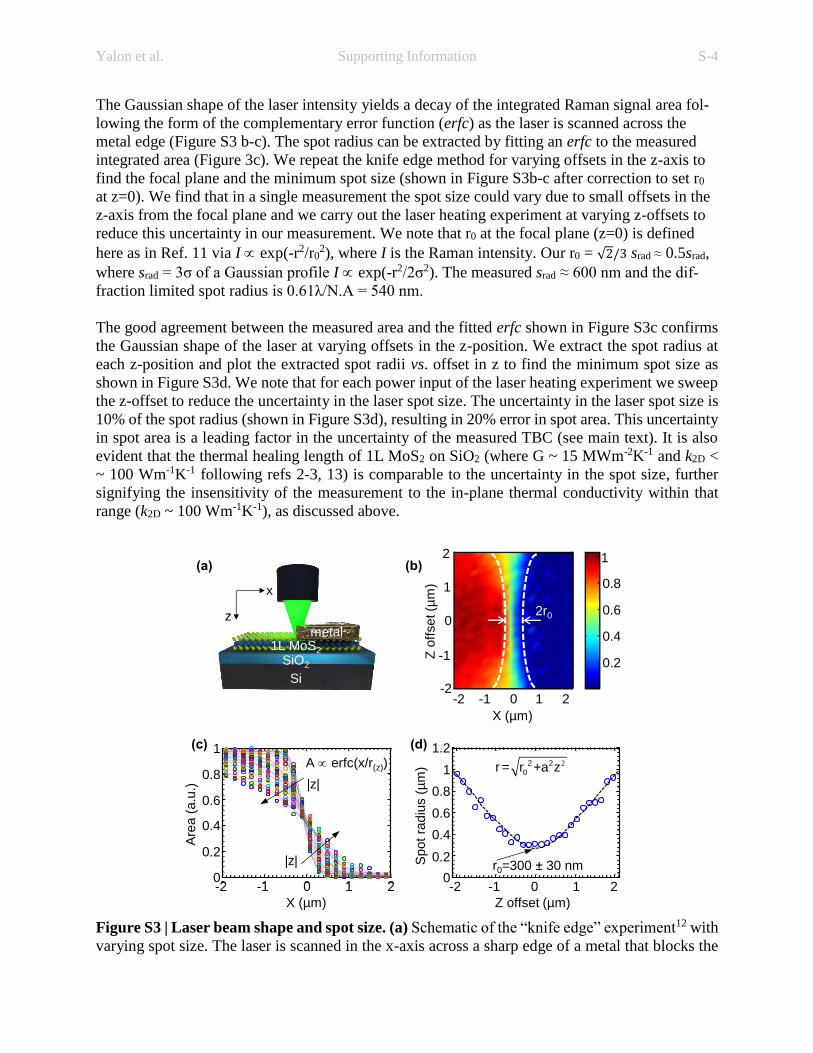
4. Heating by absorbed power in Si substrate
Thanks to the material selectivity of the Raman technique, we obtained the temperature rise in the
Si substrate during the laser heating experiment (see for example Figure 4c in the main text). The
Si substrate heats due to absorbing a fraction of the incident laser power, rather than being heated
by the MoS2. As a result, the MoS2 film is also further heated by the Si substrate as illustrated in
the simulation shown in Figure S4. It is therefore important to consider the measured Si tempera-
ture in the analysis of the TBC. The absorbed power in the Si substrate is modeled as a heat source
with a Gaussian beam shape in the radial direction and exponentially decaying intensity (Beer-
Lambert law for the absorption) in the z-axis with an absorption depth of 0.65 µm.14
Figure S4 | Absorbed power and heating of Si substrate. (a) Simulated absorbed power density
in the Si substrate during laser heating experiment. The total absorbed power is 2 mW, the laser
spot size at the Si surface is 300 nm and the absorption depth is 0.65 µm.14 To highlight the effect
of heating from the Si substrate, no absorbed power is assumed at the 2D film in this simulation.
(b) Simulated temperature profile for the power input described in (a), for which only the Si sub-
strate absorbs power. The temperature rise at the 2D film as a result of the substrate heating is
similar to the temperature rise at the top surface of the Si with some heat spreading in the SiO2.
Power input Temperature profile
Si
90 nm SiO2
2D film
P (mW/µm3)
10
5
0
2
4
6
8
10
ΔT ( C)
100 200 300 400400
500
600
700
800
SiO2 thickness (nm)
Wavele
ngth
(nm
)
0
5
10
15
20
15
20
100 200 300 400400
500
600
700
800
SiO2 thickness (nm)
Wavele
ngth
(nm
)
0
2
4
6
8
10
12
0
12

Yalon et al. Supporting Information S-6
Figure S5 | Temperature rise of MoS2 with vs. without heating from Si substrate. Simulated
temperature rise (ΔT) during laser heating experiment with absorbed power in (a) the MoS2 only
(no absorbed power in the Si substrate), and (b) both MoS2 and Si. It is evident that the absorbed
power in the Si substrate heats the MoS2 film (also shown in Figure S4), and therefore the meas-
ured temperature of the heated Si substrate must be used in the analysis of the TBC.
5. Thermal resistance of incident vs. absorbed power
Figure S6 compares the temperature rise in the laser heating experiment of 1L MoS2 with respect
to the incident and absorbed laser power. The thermal resistance of the 1L MoS2 (slope) seemingly
increases with temperature when considered with respect to the incident laser power. However,
when the temperature-dependent absorption is taken into account, the thermal resistance with re-
spect to the absorbed laser power slightly decreases, indicating that the TBC slightly increases
with temperature as reported in Figure 4 of the main text.
Figure S6 | Thermal resistance with respect to incident vs. absorbed laser power. Measured
temperature rise in CVD 1L MoS2 on SiO2(94 nm)-Si at varying stage temperatures: 25 (blue),
100 (purple), and 175 ºC (red) with respect to (a) incident, and (b) absorbed laser power. The
comparison shows that the thermal resistance of the 1L MoS2 (slope, dashed line) increases with
temperature with respect to the incident laser power, but slightly decreases with temperature with
respect to the absorbed power. The different trend is obtained due to the increased optical absorp-
tion of the MoS2 at 532 nm with temperature, see Figure 3b in main text.
0 0.5 10
0.2
0.4
0.6
0.8
1
0
20
40
60
80
No absorption in Si With absorption in Si0
20
40
60
80
ΔT ( C)ΔTmax = 90 CΔTmax = 79 C
0 2 40
20
40
60
80
100
120
Laser Power (mW)
T
(K
)
0 0.2 0.4 0.6 0.80
20
40
60
80
100
120
Absorbed Power (mW)
T
(K
)
Tstage= 25 C
Tstage= 175 CTstage= 25 C
Tstage= 175 C
0
20
40
60
ΔT
( C
) 80
100
120
0 2 4
Incident laser power (mW)
0
20
40
60
ΔT
( C
) 80
100
120
0
Absorbed power (mW)
0.2 0.4 0.6 0.8

Yalon et al. Supporting Information S-7
6. Enhancement factor of AlN-Si substrate
The intensity of the electric field of the electromagnetic wave from the laser on a given substrate
relative to the intensity of the incident electric field (of the electromagnetic wave from the laser),
termed here the enhancement factor is required to obtain the absorbed power in the supported
MoS2 film, and its calculation for SiO2-Si is shown in Figure 3 of the main text. We use transfer
matrix method for the calculations. Figure S7 below shows the enhancement factor of the AlN(185
nm)-Si stack vs. wavelength. The value 0.91 is obtained at 532 nm (shown in green) and was used
for the calculation of the absorbed power in the 1L MoS2 on AlN-Si shown in Figure 4 of the main
text.
Figure S7 | Calculated enhancement factor of AlN(185 nm)-Si substrate. Calculated enhance-
ment factor of AlN(185 nm)-Si substrate vs. wavelength. The value of 0.91 for wavelength 532
nm (laser line used in this study) is indicated and was used to calculate the power absorbed by the
1L MoS2 on AlN(185 nm)-Si substrate shown in Figure 4 of the main text.
Supporting Information References:
1. Smithe, K. K. H.; English, C. D.; Suryavanshi, S. V.; Pop, E., Intrinsic Electrical Transport
and Performance Projections of Synthetic Monolayer MoS2 Devices. 2D Mater. 2017, 4 (1),
011009.
2. Yan, R.; Simpson, J. R.; Bertolazzi, S.; Brivio, J.; Watson, M.; Wu, X.; Kis, A.; Luo, T.;
Hight Walker, A. R.; Xing, H. G., Thermal Conductivity of Monolayer Molybdenum Disulfide
Obtained from Temperature-Dependent Raman Spectroscopy. ACS Nano 2014, 8 (1), 986-993.
3. Zhang, X.; Sun, D.; Li, Y.; Lee, G.-H.; Cui, X.; Chenet, D.; You, Y.; Heinz, T. F.; Hone,
J. C., Measurement of Lateral and Interfacial Thermal Conductivity of Single-and Bilayer MoS2
and MoSe2 Using Refined Optothermal Raman Technique. ACS Appl. Mater. Interfaces 2015, 7
(46), 25923-25929.
4. Seol, J. H.; Jo, I.; Moore, A. L.; Lindsay, L.; Aitken, Z. H.; Pettes, M. T.; Li, X.; Yao, Z.;
Huang, R.; Broido, D., Two-Dimensional Phonon Transport in Supported Graphene. Science 2010,
328 (5975), 213-216.
5. Sadeghi, M. M.; Jo, I.; Shi, L., Phonon-Interface Scattering in Multilayer Graphene on an
Amorphous Support. Proc. Natl. Acad. Sci. 2013, 110 (41), 16321-16326.
400 500 600 700 8000
0.2
0.4
0.6
0.8
1
Wavelength (nm)
Enhancem
ent
532 nm
0.91

Yalon et al. Supporting Information S-8
6. Zhou, H.; Zhu, J.; Liu, Z.; Yan, Z.; Fan, X.; Lin, J.; Wang, G.; Yan, Q.; Yu, T.; Ajayan, P.
M., High Thermal Conductivity of Suspended Few-Layer Hexagonal Boron Nitride Sheets. Nano
Res. 2014, 7 (8), 1232-1240.
7. Sichel, E.; Miller, R.; Abrahams, M.; Buiocchi, C., Heat Capacity and Thermal
Conductivity of Hexagonal Pyrolytic Boron Nitride. Phys. Rev. B 1976, 13 (10), 4607.
8. Jo, I.; Pettes, M. T.; Kim, J.; Watanabe, K.; Taniguchi, T.; Yao, Z.; Shi, L., Thermal
Conductivity and Phonon Transport in Suspended Few-Layer Hexagonal Boron Nitride. Nano Lett.
2013, 13 (2), 550-554.
9. Perichon, S.; Lysenko, V.; Remaki, B.; Barbier, D.; Champagnon, B., Measurement of
Porous Silicon Thermal Conductivity by Micro-Raman Scattering. J. Appl. Phys. 1999, 86 (8),
4700-4702.
10. Balandin, A. A.; Ghosh, S.; Bao, W.; Calizo, I.; Teweldebrhan, D.; Miao, F.; Lau, C. N.,
Superior Thermal Conductivity of Single-Layer Graphene. Nano Lett. 2008, 8 (3), 902-907.
11. Cai, W.; Moore, A. L.; Zhu, Y.; Li, X.; Chen, S.; Shi, L.; Ruoff, R. S., Thermal Transport
in Suspended and Supported Monolayer Graphene Grown by Chemical Vapor Deposition. Nano
Lett. 2010, 10 (5), 1645-1651.
12. Mauck, M., Knife-edge profiling of Q-Switched Nd: YAG Laser Beam and Waist. Appl.
Opt. 1979, 18 (5), 599-600.
13. Yalon, E.; McClellan, C. J.; Smithe, K. K.; Munoz Rojo, M.; Xu, R. L.; Suryavanshi, S.
V.; Gabourie, A. J.; Neumann, C. M.; Xiong, F.; Farimani, A. B.; Pop, E., Energy Dissipation in
Monolayer MoS2 Electronics. Nano Lett. 2017, 17, 3429–3433.
14. Jellison Jr, G. E.; Modine, F. A.; White, C. W.; Wood, R. F.; Young, R. T., Optical
Properties of Heavily Doped Silicon Between 1.5 and 4.1 eV. Phys. Rev. Lett. 1981, 46 (21), 1414.