Embed Size (px)
Citation preview

Technical Report July 29, 2011
A Practicable Method for Thickness Estimation of Ultrathin Layers from XPS Data with UNIFIT 2011 P. Streubel, R. Hesse, L. Makhova, J. Schindelka and R. Denecke
Wilhelm-Ostwald-Institut für Physikalische und Theoretische Chemie, Universität Leipzig, Linnéstr. 2, D-04103 Leipzig, Germany
Abstract The thickness of laterally homogeneous films in the range of few nm may be estimated by quantitative analysis of XPS measurements of two substrate signals of photoelectron peaks of the covered substrate at different kinetic energies with fixed experimental conditions. Intensities of the pure substrate elements are not required. The method is tested by measurements on a generated Fe/Cu model system and studies of industrially produced GaAs-oxide layers. The easy analysis of the XPS data using the software UNIFIT 2011 with predetermined spectrometer transmission functions is demonstrated. The usefulness of the presented method for practical layer thickness estimation is shown.
Keywords XPS, Photoelectron spectroscopy, Layer thickness, Quantification, Spectrum analysis, Substrate signals, Processing software, UNIFIT
__________________________________________________________________________
P. Streubel, R. Hesse*, L. Makhova, J. Schindelka, R. Denecke Wilhelm-Ostwald-Institut für Physikalische and Theoretische Chemie, Universität Leipzig, Linnéstr. 2, D-04103 Leipzig, Germany. e-mail: [email protected]

2
Introduction The determination of the thickness of ultrathin layers on solids, e.g. metals or oxides on semiconductors, is very important for development of processes and production control. In many cases the thickness of protection or contamination layers at the surface is in the range of less than 1 nm up to 10 nm. This is the information depth of x-ray photoelectron spectroscopy (XPS) with typical excitation energies of about 1.5 keV. XPS does not permit exclusively the analysis of the chemical composition of surfaces and their contaminations. Additionally, the thickness of films with well known structures can be determined. For the most commonly used method of thickness determination of thin films the intensity ratio of photoelectron peaks of the layer and the substrate is applied. In the present work we recommend the more practicable method for thickness estimation of ultrathin layers by XPS using two peaks at different energies of a single substrate element only. This method is rarely applied. We use the improved quantitative XPS analysis with predetermined spectrometer transmission functions. Furthermore we use the attenuation length of the photoelectrons considering the elastic scattering of these electrons instead of the generally applied inelastic mean free path of the photoelectrons. The easy operation applying this method, implemented in the processing software UNIFIT 2011, is demonstrated. Two different sample systems are tested. The advantages and disadvantages of the method are discussed. Method of thickness estimation by substrate intensities For the thickness estimation of a layer A on a substrate B the influence of the layer thickness, the energy dependent attenuation length, or the emission angle of the photoelectrons on their photoemission intensities are used. In the simple case of a homogeneous layer of the thickness d of the element A on a substrate B the layer and the substrate intensities IA or IB are given [1] by:
−−= ∞ θλ cos
exp1,AA
AA
dII (1)
−= ∞ θλ cos
exp,AB
BB
dII (2)
where IA∞ and IB∞ are the intensities of the pure bulk elements A and B. λA,A and λB,A are the inelastic mean free paths (better: the attenuation lengths AL considering the elastic scattering of the photoelectrons) of the electrons in A (second index letter) emitted by the element A or B (first index letter). The emission angle θ of the electrons is given with respect to the surface normal (polar angle). Eqs. 1 and 2 are defined according to the following assumptions:
- The samples are homogeneous and flat. - The interfaces are abrupt. - The samples are fine-grained or amorphous, which means that the photoelectrons do not
show interference effects. In order to reduce the uncertainties of the thickness estimation, evaluation methods using the intensity ratios, e.g. IA/IB, are mostly preferred [2, 3]. For the most commonly used method of thickness determination of thin films the intensity ratio IA/IB of photoelectron peaks of the layer A and the substrate B is applied (Method 1) [2]:
3
)]cos/(exp[
)]}cos/(exp[1{
,
,
θλθλ
ABB
AAA
B
A
dI
dI
I
I
−−−
=∞
∞ (3)
with the intensity ratio of the bulk elements A and B [3]
BBBBB
AAAAA
B
A
TN
TN
I
I
,
,
λσλσ
=∞
∞ (4)
where N is the atomic density, σ is the ionization cross-section of the observed photoelectron line and T is the transmission function of the spectrometer (also called intensity/energy response function [IERF]). With the corrected intensity [3]
T
II
σλ=' (5)
the ratio is given by
)]cos/(exp[
)]}cos/(exp[1{
'
'
,
,
θλθλ
ABB
AAA
B
A
dN
dN
I
I
−−−
= (6)
With the approximation λA,A ≈ λB,A = λ [2, 4], we can write for the layer thickness d:
+=
+=
∞
∞ 1lncos1'
'lncos
AB
BA
AB
BA
II
II
NI
NId θλθλ (7)
The accuracy of d using Eq. 7 is affected by NB/NA or by IB∞/IA∞. Especially for a more complex layer the atomic density NA of the element A in the layer or the intensity IA∞ of a bulk reference sample of the layer cannot be determined easily [2]. Furthermore, the approximation for λ can impinge on the accuracy of d. Recently, a multiline method was tested to improve the accuracy of Method 1 [4]. Two different lines of the Ni overlayer and one line of the Au substrate were measured. Jablonski and Zemek [4] expect that this procedure is more accurate due to the fact that the systematic errors are averaged. Appropriate thickness results based on a simpler experiment may be expected by using substrate intensities only of two different photoelectron peaks of the same element at the energies E1 and E2, exhibiting sufficiently large differences in λ. This method (Method 2) was recommended by M. Ebel et al. [5] and S. Hofmann [6] and applied by R. W. Bernstein et al. [7], O. M. Mikhailik et al. [8] and Ts. Mihailova et al. [9]. We have tested the Method 2 in this paper. Thereby the improved quantitative XPS analysis using the predetermined spectrometer transmission function [3] was applied. From Eq. 2 the intensity ratio of the two substrate peaks is given by
)cos)(/exp()(
)cos)(/exp()(
)(
)(
22
11
2
1
θλθλ
EdEI
EdEI
EI
EI
AB
AB
B
B
−⋅−⋅
=∞
∞ (8)
where λA(Ei) is the attenuation length of the substrate electrons with kinetic energy Ei in the overlayer (element) A. The ratio of the measured intensities of the bulk material B for E1 and E2 is given by

4
)()()(
)()()(
)(
)(
222
111
2
1
ETEE
ETEE
EI
EI
BBB
BBB
B
B
λσλσ
=∞
∞ (9)
With the definition of the corrected intensity I’ of the electron peak from Eq. 5 the ratio of the corrected measured intensities of the pure bulk element B becomes I’ B∞(E1)/ I’ B∞(E2) = 1 and that of the covered substrate B
)cos)(/exp(
)cos)(/exp(
)('
)('
2
1
2
1
θλθλ
Ed
Ed
EI
EI
A
A
B
B
−−
= (10)
Finally the equation for the determination of d is:
)('
)('ln
)()(
)()(cos
2
1
21
21
EI
EI
EE
EEd
B
B
AA
AA
λλλλθ
−= (11)
Therefore, the estimation of the film thickness of a covered sample using Method 2 requires only the intensities IB(E1) and IB(E2) of the substrate measured at the same experimental conditions. The measurement of the pure bulk substrate is not necessary. Additionally, the influences due to changes in elastic electron scattering and roughness of the sample are minimised. The atomic density ratio of layer and substrate NA/NB in Eq. 7, hardly determined with satisfying accuracy [2], is also eliminated. Uncertainties of d arising from Eq. 11 are determined mainly by the uncertainty of λ in the “λ term” λA(E1)·λA(E2)/[λA(E1)-λA(E2). The value of λ is strongly affected by the electron scattering and overlayer composition and density. We used the average practical effective attenuation length Lave [10] instead of λA in Eq. 11. Lave considering the elastic scattering of electrons seems to be the best approximation for practical use of the electron effective attenuation length (EAL). We have tested Lave for a Ni layer on Au substrate. This layer system was investigated by Jablonski and Zemek [4] with a reliable, but time-consuming Monte Carlo calculation of EAL. We found with Eq. 2 and λAu,Ni = Lave = 13.4 Å for Au 4f photoelectrons in Ni a good agreement of the d values (no more than 10% difference compared to the results of Jablonski and Zemek [4] in their Table 5). Method 2 using an excitation energy of about 1.5 keV is limited to very thin layers (d ≤ 3λ ≈ 3 nm) by the quotient λA(E1)·λA(E2)/[λA(E1)-λA(E2)] with suffiently large λ differences. Thicknesses up to 20 nm could be estimated with High Kinetic Energy XPS (HIKE-XPS) utilizing the increase of the λ values. The determination of the corrected intensities I’ B(E1)/I’ B(E2) in Eq. 11 with Eqs. 4 and 5 requires a well calibrated electron transmission function T(E) [3] of the spectrometer. Furthermore the σ(E) values calculated by Scofield [11] are used for the sensitivity factor σ·λ·T. For the λ values the approximation [3] λ ≈ 0.103 E0.745 (12) gives with the quotient λB(E2)/λB(E1) satisfying results for the corrected intensities I’ B(E1)/I’ B(E2). This was shown by Hesse et al. [3] for a test sample and was tested in the analytical practice of our laboratory, too. Generally, the use of ratios T(E2)/T(E1), σ(E2)/σ(E1) and λB(E2)/λB(E1) reduces the uncertainty of the corrected intensities. Not all chemical elements have two available photoelectron lines at two different energies within the available energy range. In such a case the second peak can be an appropriate Auger line I∞(E2). The relevant σAuger(E2) value can be determined from Eq. 9 with the known σ(E1),

5
λ(E1) and T(E1) of the measured photoelectron intensity I∞(E1) and λ(E2) and T(E2) of the measured Auger peak intensity I∞(E2) of the pure bulk substrate B:
)()(
)()()(
)(
)()(
22
111
1
22 ETE
ETEE
EI
EIEAuger λ
λσσ∞
∞= (13)
An alternative way is using the variable excitation energy of a synchrotron source to create intensity values for two different kinetic energies for a single core level. With the Method 2 by tuning the excitation energy (Excitation-energy resolved XPS, ERXPS) already depth profiles were created based on an extensive calculation, [12, 13]. A data treatment algorithm has been developed in which intensity information acquired for different excitation energies was modelled with hypothetical depth distribution functions of the species studied. For excitation with Al Kα or Mg Kα sources the difference E1 – E2 should be between 300 and 1200 eV and the “λ term” λA(E1) λA(E2)/ [λA(E1)-λA(E2)] should be between 4 and 30 Å to obtain a valuable intensity quotient I’(E1)/I’(E2) using Eq. 11. These conditions are not given for all elements of the periodic table. However, more than 60 chemical elements can create a substrate with these conditions.
Experimental Samples For testing Method 2 two layer systems were selected:
i) a generated model system of Fe layers on Cu substrate and ii) an industrially produced series of oxidized GaAs(100) samples.
i) The Fe/Cu samples were generated in situ by electron beam evaporation of Fe on a Cu foil in the preparation chamber of the photoelectron spectrometer. The Cu metallic foil was cleaned ex situ by hydrochloric acid, rinsed with ethanol and cleaned in an ultrasonic bath. After installation in the UHV preparation chamber the Cu foil was sputtered for 5 minutes with 5 keV Ar+ ions. The iron layer was evaporated step by step from iron powder (99.998 %, Alfa Aesar). The evaporation rate of Fe was estimated with Method 2 to about 3 Å/min. ii) An n-type GaAs(100) substrate covered with a native oxide layer was oxidized additionally by UV-ozone ex situ at different UV exposing times: 10, 45 and 90 s. A low carbon contamination was always found. Spectrometer The measurements were performed using an X-ray photoelectron spectrometer VG ESCALAB 220 iXL. This spectrometer is equipped with a model 220 analyser and a set of six channel electron multipliers. The 180° analyser is equipped with one magnetic and six electrostatic lenses and two mechanical apertures. In this work, the energy scale was calibrated to ±0.02 eV (ISO 15472). The charge correction for the GaAs samples was estimated with C 1s = 285.0 eV. The instrument was operated in the CAE mode (constant ∆E) at pass energies of 50 eV and 10 eV. The angle of the X-ray sources with respect to the surface normal was 55° for the Al/Mg Twin and 58° for the Al Mono. The base pressure during all experiments was 5·10-8 Pa. The transmission functions T(E) of the spectrometer for different pass energies and lens modes were determined by the quantified peak-area approach (QPA) [3]. The number of scans is varied between 3 and 5, but was equal for different spectra of an experiment. In order to minimise the time-drift error of
6
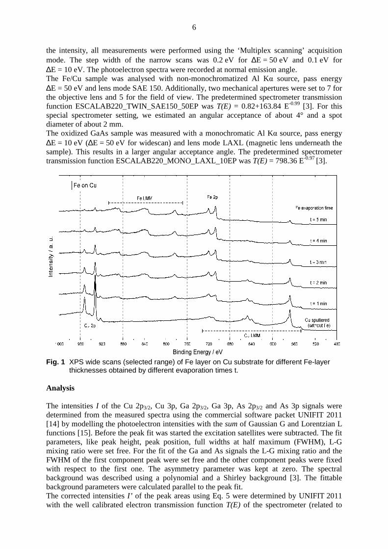
the intensity, all measurements were performed using the ‘Multiplex scanning’ acquisition mode. The step width of the narrow scans was 0.2 eV for ∆E = 50 eV and 0.1 eV for ∆E = 10 eV. The photoelectron spectra were recorded at normal emission angle. The Fe/Cu sample was analysed with non-monochromatized Al Kα source, pass energy ∆E = 50 eV and lens mode SAE 150. Additionally, two mechanical apertures were set to 7 for the objective lens and 5 for the field of view. The predetermined spectrometer transmission function ESCALAB220_TWIN_SAE150_50EP was T(E) = 0.82+163.84 E-0.99 [3]. For this special spectrometer setting, we estimated an angular acceptance of about 4° and a spot diameter of about 2 mm. The oxidized GaAs sample was measured with a monochromatic Al Kα source, pass energy ∆E = 10 eV (∆E = 50 eV for widescan) and lens mode LAXL (magnetic lens underneath the sample). This results in a larger angular acceptance angle. The predetermined spectrometer transmission function ESCALAB220_MONO_LAXL_10EP was T(E) = 798.36 E-0.97 [3].
Fig. 1 XPS wide scans (selected range) of Fe layer on Cu substrate for different Fe-layer
thicknesses obtained by different evaporation times t. Analysis The intensities I of the Cu 2p3/2, Cu 3p, Ga 2p3/2, Ga 3p, As 2p3/2 and As 3p signals were determined from the measured spectra using the commercial software packet UNIFIT 2011 [14] by modelling the photoelectron intensities with the sum of Gaussian G and Lorentzian L functions [15]. Before the peak fit was started the excitation satellites were subtracted. The fit parameters, like peak height, peak position, full widths at half maximum (FWHM), L-G mixing ratio were set free. For the fit of the Ga and As signals the L-G mixing ratio and the FWHM of the first component peak were set free and the other component peaks were fixed with respect to the first one. The asymmetry parameter was kept at zero. The spectral background was described using a polynomial and a Shirley background [3]. The fittable background parameters were calculated parallel to the peak fit. The corrected intensities I’ of the peak areas using Eq. 5 were determined by UNIFIT 2011 with the well calibrated electron transmission function T(E) of the spectrometer (related to
7
E = 1000 eV) [3], σ(E) values of Scofield (related to σ for C 1s) [11] and approximated λ values [3] according to Eq.12.
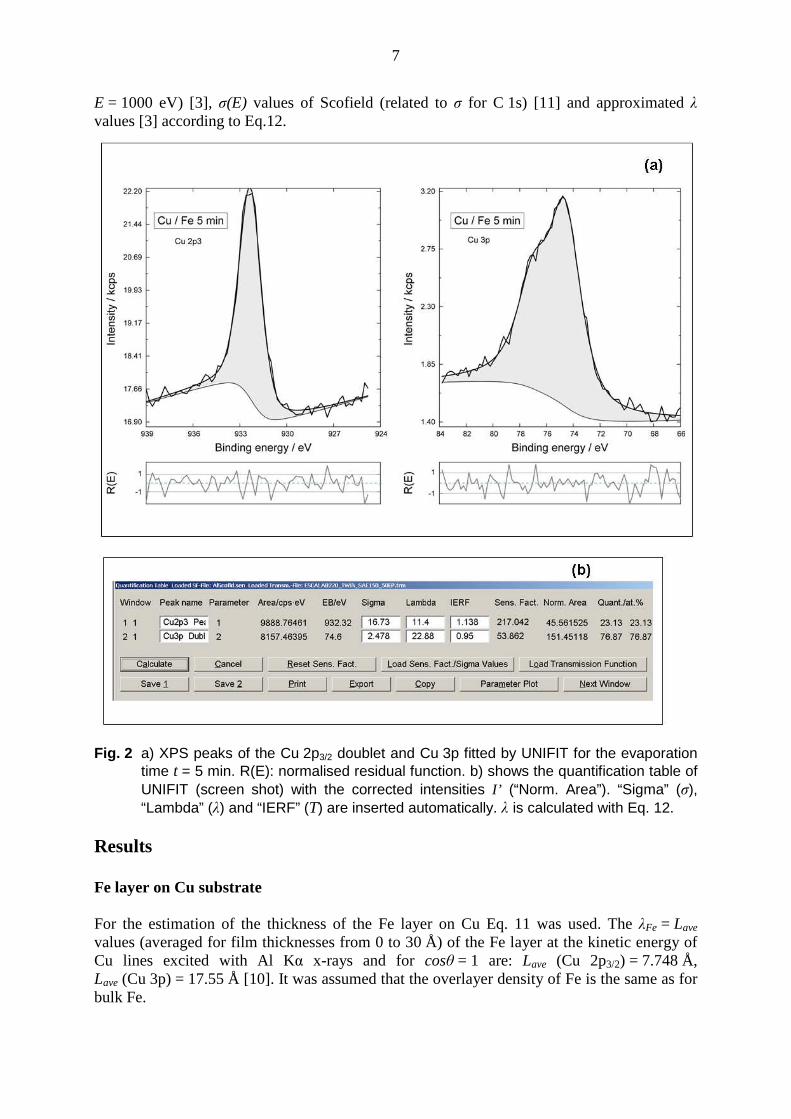
Fig. 2 a) XPS peaks of the Cu 2p3/2 doublet and Cu 3p fitted by UNIFIT for the evaporation
time t = 5 min. R(E): normalised residual function. b) shows the quantification table of UNIFIT (screen shot) with the corrected intensities I’ (“Norm. Area”). “Sigma” (σ), “Lambda” (λ) and “IERF” (T) are inserted automatically. λ is calculated with Eq. 12.
Results Fe layer on Cu substrate For the estimation of the thickness of the Fe layer on Cu Eq. 11 was used. The λFe = Lave values (averaged for film thicknesses from 0 to 30 Å) of the Fe layer at the kinetic energy of Cu lines excited with Al Kα x-rays and for cosθ = 1 are: Lave (Cu 2p3/2) = 7.748 Å, Lave (Cu 3p) = 17.55 Å [10]. It was assumed that the overlayer density of Fe is the same as for bulk Fe.
8
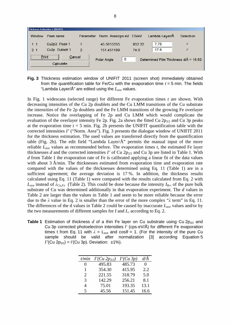
Fig. 3 Thickness estimation window of UNIFIT 2011 (screen shot) immediately obtained
from the quantification table for Fe/Cu with the evaporation time t = 5 min. The fields “Lambda Layer/Å” are edited using the Lave values.
In Fig. 1 widescans (selected range) for different Fe evaporation times t are shown. With decreasing intensities of the Cu 2p doublets and the Cu LMM transitions of the Cu substrate the intensities of the Fe 2p doublets and the Fe LMM transitions of the growing Fe overlayer increase. Notice the overlapping of Fe 2p and Cu LMM which would complicate the evaluation of the overlayer intensity Fe 2p. Fig. 2a shows the fitted Cu 2p3/2 and Cu 3p peaks at the evaporation time t = 5 min. Fig. 2b presents the UNIFIT quantification table with the corrected intensities I’ (“Norm. Area”). Fig. 3 presents the dialogue window of UNIFIT 2011 for the thickness estimation. The used values are transferred directly from the quantification table (Fig. 2b). The edit field “Lambda Layer/Å” permits the manual input of the more reliable Lave values as recommended before. The evaporation times t, the estimated Fe layer thicknesses d and the corrected intensities I’ of Cu 2p3/2 and Cu 3p are listed in Table 1. With d from Table 1 the evaporation rate of Fe is calibrated applying a linear fit of the data values with about 3 Å/min. The thicknesses estimated from evaporation time and evaporation rate compared with the values of the thicknesses determined using Eq. 11 (Table 1) are in a sufficient agreement; the average deviation is 17 %. In addition, the thickness results calculated using Eq. 11 (Table 1) were compared with the results calculated from Eq. 2 with Lave instead of λCu,Fe (Table 2). This could be done because the intensity IB∞ of the pure bulk substrate of Cu was determined additionally in that evaporation experiment. The d values in Table 2 are larger than the values in Table 1 and seem to be more reliable because the error due to the λ value in Eq. 2 is smaller than the error of the more complex “λ term” in Eq. 11. The differences of the d values in Table 2 could be caused by inaccurate Lave values and/or by the two measurements of different samples for I and I∞ according to Eq. 2. Table 1 Estimation of thickness d of a thin Fe layer on Cu substrate using Cu 2p3/2 and
Cu 3p corrected photoelectron intensities I’ (cps·eV/Å) for different Fe evaporation times t from Eq. 11 with λ = Lave and cosθ = 1. (For the intensity of the pure Cu sample should be valid after normalization [3] according Equation 5 I’ (Cu 2p3/2) = I’(Cu 3p). Deviation: ±1%).
t/min I’(Cu 2p3/2) I’(Cu 3p) d/Å 495.83 485.73 0 0
1 354.30 415.95 2.2 2 221.55 318.79 5.0 3 142.29 256.21 8.1 4 75.01 193.35 13.1 5 45.56 151.45 16.6

9
Table 2 Estimation of thickness d of a thin Fe layer on Cu substrate for different Fe evaporation times t from Eq. 2 with λ = Lave and cosθ = 1. For I’ see Table 1.
t/min d/Å with I’(Cu 2p3/2)
d/Å with I’(Cu 3p)
0 0 0 1 2.6 2.7 2 6.2 7.4 3 9.7 11.2 4 14.6 16.2 5 18.5 20.5
Fig. 4 Change of the fitted XPS peak Ga 2p3/2
for different ozone-exposition times t of GaAs(100).
Thin oxide layer on GaAs(100) substrate The layer of oxidized GaAs is a mixture of different oxidation products of GaAs and a carbon contamination. The Lave values [10] can be determined approximately only for a GaAs layer and not for the overlayer of the complex composition. We assumed that the difference of composition and density between GaAs and the overlayer do only have a small influence on the electron attenuation (as found for a Ga2O3 overlayer). The Lave values (averaged for film thicknesses from 0 to 30 Å) for photoelectrons of Ga and As with Al Kα excitation and

10
cosθ = 1 are: Lave (Ga 2p3/2) = 8.057 Å, Lave (Ga 3d) = 25.64 Å, Lave (As 2p3/2) = 4.769 Å and Lave (As 3d) = 25.30 Å [10].
Fig. 5 XPS widescan GaAs(100) with overlayer after ozone exposition with t = 45 s. The modification of the GaAs surface after different ozone-exposition times, indicated by the changing Ga 2p3/2 signal, is shown in Fig. 4. The small GaO and Ga2O3 peaks of the very thin oxide layer at the beginning increase with the ozone-exposition time whereas the GaAs peaks decrease. The Figs. 4 and 6 represent plots of the measured spectra of GaAs with an ozone-oxidation time of 45 s (GaAs / Ozone 45 s). The widescan (Fig. 5) shows the large energy difference between the 3d and 2p3/2 peaks of Ga and As favourable to overlayer thickness determination and also a small C 1s peak originating from contamination. The fit of the 2p3/2 and 3d peaks of Ga and As displays different chemical species of Ga and As. The Ga oxidation products of GaAs are indentified as GaO and Ga2O3, the As oxidation products of GaAs as As, AsO, As2O3 and As2O5. As examples the fitted spectra for the ozone-exposition time of 45 s are shown (Fig. 6a-d). The chemical shifts are in good agreement with the studies of Flynn and McIntyre [16] and Schaufuss et al. [17]. The peak areas I’ (“Norm. Area”) used for the quantification are taken from the quantification tables of the fitted spectra of Ga, As, O and C (examples of the UNIFIT quantification tables for the ozone-exposition time of 45 s: Tables 3 and 4). Due to the very low kinetic energy E (large binding energy EB) and therefore the high surface sensitivity (small λ) of the Ga 2p3/2 and As 2p3/2 peaks, relatively large peaks for the components of oxidation are obtained from the peak fit (Figs. 6b and d, Table 4). In contrast, the components of oxidation estimated from the fit of the Ga 3d and As 3d peaks (Figs. 6a and c, Table 3) are significantly lower. For estimation of the thickness d the values “Norm. Area” (corrected intensity I’ ) of the GaAs substrate components of the peak fit of the Ga 3d, Ga 2p3/2, As 3d and As 2p3/2 spectra are used. Fig. 7 shows the screen shot of the thickness estimation dialogue of UNIFIT 2011. The used values of I’ (“Norm. Area”) and EB are transferred directly from the quantification table presenting the layer thickness for the ozone-exposition time t = 45 s (Tables 3 and 4). The default values in the field “Lambda Layer/Å” were substituted by the more reliable Lave values, the λ values of the non selected peaks were set to 0.

11
Fig. 6 Fitted XPS peaks of GaAs(100) with overlayer after ozone-exposition time t = 45 s,
a) Ga 3d doublets, b) Ga 2p3/2 peaks, c) As 3d doublets and d) As 2p3/2 peaks. The estimated thicknesses d of the overlayers (oxides and carbon contamination) on GaAs substrate are shown in Table 5. Four samples with different ozone oxidation times (0, 10, 45 and 90 s) were investigated. The layer thickness values d are estimated with the GaAs substrate components of Ga 3d and Ga 2p3/2 (Fig. 6a and b) as well as the As 3d and As 2p3/2 peaks (Fig. 6c and d). The fairly good agreement between the Ga and As results demonstrates the usefulness of the presented method (Table 5). The remarkable deviation between the d values obtained from the Ga and As peaks in the case of 0 and 90 s ozone treatment could be caused by the peak-fit uncertainties of the Ga and As peaks containing three or five single peaks, by the small kinetic energy E(As 2p3/2) inducing uncertainties of λ in Eq. 12 used for I’ and/or by a non ideal interface. In practice, the rounded average of both results calculated using Ga and As peaks should reduce the error. Furthermore one has to take into account that the accuracy of the absolute values of d is influenced by the overlayer density usually deficient known. The thickness estimation of the overlayer on GaAs according to Eq. 2 is not possible because pure GaAs was not available and is difficult to prepare. For more insight in the possible layer structure we tried to prove the thickness of the carbon contamination. It is assumed that the carbon found (Tables 3 and 4: -CH2, -CO-) forms the
(a) (b)
(c) (d)
12
contamination layer on the top of the sample covering the layer of the oxidation products of GaAs. For estimation of the thickness d of the carbon layer the sum of I’ of all Ga or As components is used. Lave (averaged for film thicknesses from 0 to 10 Å) are determined for the Ga and As photoelectrons with Al Kα excitation and cosθ = 1 in a carbon layer: Lave (Ga 2p3/2) = 11.47 Å, Lave (Ga 3d) = 35.12 Å, Lave (As 2p3/2) = 6.245 Å and Lave (As 3d) = 34.69 Å [10]. Table 3 Atomic concentrations and the corrected intensities I’ (“Norm.Area”) calculated from
the As 3d (Fig. 6c), Ga 3d (Fig. 6a), C 1s and O 1s peaks of a GaAs sample after 45 s ozone oxidation (from the quantification table of UNIFIT; Quant./at.%: homogeneous sample assumed).
Peak name
EB / eV Norm. Area
Quant. / at.%
As 3d GaAs 41.4 54.84 21.76 27.52 As 3d As 42.8 0.77 0.31 As 3d AsO 44.3 3.73 1.48 As 3d As2O3 44.8 6.09 2.42 As 3d As2O5 46.0 3.91 1.55 Ga 3d GaAs 19.6 60.07 23.84 29.54 Ga 3d GaO 20.2 8.92 3.54 Ga 3d Ga2O3 21.1 5.44 2.16 C 1s -CH2- 284.9 19.31 7.66 15.45 C 1s -C*H2-C-O- 285.4 9.75 3.87 C 1s -C-O- 286.7 9.87 3.92 O 1s Oxide 1 531.5 46.24 18.35 27.50 O 1s Oxide 2 532.5 23.06 9.15
Table 4 Atomic concentrations and the corrected intensities I’ (“Norm.Area”) from the
As 2p3/2 (Fig. 6d), Ga 2p3/2 (Fig. 6b), C 1s and O 1s peaks of a GaAs sample after 45 s ozone oxidation (from the quantification table of UNIFIT; Quant./at.%: homogeneous sample assumed).
Peak name
EB / eV Norm. Area
Quant. / at.%
As 2p3/2 GaAs 1323.3 10.99 5.34 22.33 As 2p3/2 As 1324.7 1.72 0.83 As 2p3/2 AsO 1326.1 12.21 5.93 As 2p3/2 As2O3 1326.8 13.67 6.63 As 2p3/2 As2O5 1327.8 7.43 3.60 Ga 2p3/2 GaAs 1117.7 27.09 13.15 25.15 Ga 2p3/2 GaO 1118.6 15.86 7.70 Ga 2p3/2 Ga2O3 1119.2 8.86 4.30 C 1s -CH2- 284.9 19.31 9.37 18.89 C 1s -C*H2-C-O- 285.4 9.75 4.73 C 1s -C-O- 286.7 9.87 4.79 O 1s Oxide 1 531.5 46.24 22.44 33.63 O 1s Oxide 2 532.5 23.06 11.19

13
Fig. 7 Thickness estimation window of UNIFIT 2011 (screen shot) with the determined layer
thickness of the GaAs overlayer for ozone-exposition time t = 45 s from Ga 2p3/2 and Ga 3d. The fields “Lambda Layer/Å” for the GaAs component are edited using the Lave values. The λ values of the non selected peaks were set to 0.
The results are shown in Table 6 and in Fig. 8. The carbon layer thickness is in the same order of magnitude as the layer of the oxidation products of GaAs. Before the ozone treatment the carbon layer is thicker than the layer of the oxidation products of GaAs. With the ozone treatment the thickness of the carbon layer decreases and that of the oxidation products of GaAs increases. Conclusions We promote a rarely applied method of thickness estimation of very thin homogeneous overlayers from XPS data for practicable application. In contrast to other methods the relative intensities of two photoelectron lines of one element of the substrate at different energies are used only [5]. The overlayer thickness d on the covered substrate is obtained with UNIFIT 2011 immediately from the concentration table of the fitted peaks using a predetermined spectrometer transmission function [3]. The measurement of the pure bulk substrate is not necessary. The easy handling of the thickness calculation with the software UNIFIT 2011 was shown. Table 5 Estimation of the thickness d of a thin overlayer (oxidation products of GaAs and
carbon contamination) on GaAs substrate using the corrected photoelectron intensities I’ (cps·eV/Å) of the GaAs component of Ga 2p3/2, Ga 3d, As 2p3/2 and As 3d for different ozone treatment times t from Eq. 11 with λ = Lave and cosθ = 1.
The d values derived from Ga and As spectra are averaged and rounded to d .
t/s I’(Ga 3d, GaAs)
I’(Ga 2p3/2, GaAs)
d/Å I’(As 3d, GaAs)
I’(As 2p3/2, GaAs)
d/Å rounded d /Å
0 58.28 35.26 5.90 54.63 15.44 7.43 7 10 62.10 34.92 6.76 55.92 15.96 7.37 7 45 60.07 27.09 9.35 54.84 10.99 9.44 9 90 45.35 19.73 9.78 39.40 4.74 12.45 11

14
Table 6 Estimation of the thickness d of a thin carbon contamination overlayer (-CH2-,
-C-O-) on the layer of oxidation products of GaAs and on GaAs substrate using the corrected photoelectron intensities I’ (cps·eV/Å) of all Ga and As components of Ga 2p3/2 and Ga 3d as well as As 2p3/2 and As 3d for different ozone treatment times t from Eq. 11 with λ = Lave and cosθ = 1. The d values derived from Ga and As
spectra are averaged and rounded to d .
Fig. 8 Scheme of estimated thicknesses of the carbon contamination layer (-CH2-, -C-O-)
and the layer of the oxidation products of GaAs for different ozone treatment (see Tables 5 and 6).
Uncertainties of the thickness estimation are affected by non ideal layer/substrate systems and errors of the inelastic mean free paths (electron effective-attenuation lengths) λ of the photoelectrons. We recommend the NIST electron effective-attenuation length values [10], which include the elastic scattering effects. Unfortunately, not all chemical elements have two usable photoelectron lines with a sufficiently large energy separation. If only one photoelectron line is available, an appropriate Auger line may be used. The required ionization cross-section of the Auger line is determined easily with the software UNIFIT 2011. In this manner more than 60 elements of the periodic table of the elements may be suitable as a substrate for the thickness estimation experiments. The usefulness of the method was demonstrated by means of two examples. The results for a model system of evaporated Fe layers on Cu substrate estimated using the intensities of the Cu 3p and Cu 2p3/2 peaks from the covered sample only (Eq. 11) were compared with the results from Cu 3p and Cu 2p3/2 intensities of both the covered and pure bulk Cu substrate
t/s I’(Ga 3d) I’(Ga 2p3/2) d/Å I’(As 3d) I’(As 2p3/2) d/Å rounded d /Å
0 68.42 48.38 5.9 63.34 41.84 3.2 4.5 10 72.46 54.85 4.7 66.69 48.62 2.4 3.5 45 74.43 51.81 6.2 69.34 46.02 3.1 4.5 90 65.34 56.74 2.4 58.39 45.39 1.9 2
15
(Eq. 2). The thicknesses agree fairly well, also with the results applying evaporation time and evaporation rate of Fe. An applied sample series of modified GaAs(100) substrates with an oxidic overlayer obtained by ozone oxidation was tested as a second example. The thicknesses of the inhomogeneous layer of oxidation products of GaAs and of the carbon contamination calculated with the Ga and As peaks agree fairly well with each other. A deviation may be caused by sample inhomogenities as well as Lave and peak fit uncertainties. For estimation of the thickness d for the carbon layer only the sum of I’ of all Ga or As components is used. The carbon layer thickness is in the same order of magnitude as the layer of the oxidation products of GaAs. Realistic samples with inhomogeneous layer structure, special overlayer density, broadened interface and surface roughness decrease the accuracy of the absolute results. But the order of magnitude of d and the change of d in dependence on the treatment of the sample give informative results for technology. In the case of GaAs with an overlayer only the recommended method was applicable because the primary sample was already covered by a thin oxide layer and pure GaAs was not available and is difficult to prepare. The comparisons demonstrate a satisfying agreement of the results and with it the usefulness of the presented method for practical application.
Acknowledgements The authors thank the reviewers for the useful comments and suggestions. References 1. Seah MP (1983) p 211 In: Briggs D, Seah MP(eds.), Practical Surface Analysis, John
Wiley, Chichester 2. Seah MP, Spencer SJ (2002) Surf Interface Anal 33:640 3. Hesse R, Streubel P, Szargan R (2005) Surf Interface Anal 37:589 4. Jablonski A, Zemek J (2009) Surf Interface Anal 41:193 5. Ebel MF (1980) Surf Interface Anal 2:173 6. Hofmann S (1983) p 168 In: Briggs D, Seah MP (eds.), Practical Surface Analysis, John
Wiley, Chichester 7. Bernstein RW, Grepstad JK (1989) Surf Interface Anal 14:109 8. Mikhailik OM, Pankratov YuV, Bakai EA, Senkevich AI, Shpak AP (1995) J Electron
Spectrosc Related Phenom 76:695 9. Mihailova Ts, Velchev N, Krastev V, Marinova Ts (1997) Appl Surf Sci 120:213 10. Powell CJ, Jablonski A (2001) NIST Electron Effective-Attenuation-Length Database
Version 1.0, Standard Reference Database 82, US Department of Commerce, National Institute of Standards and Technology, Gaithersburg, Maryland
11. Scofield JH (1976) J Electron Spectrosc Related Phenom 8:129 12. Zier M, Oswald S, Reiche S, Wetzig K (2007) Microchim Acta 156:99 13. Merzlikin SV, Tolkachev NN, Strunskus T, Witte G, Glogowski T, Wöll C, Grünert W
(2008) Surf Sci 602:755 14. Hesse R (2010) UNIFIT FOR WINDOWS: Spectrum Processing, Analysis and
Presentation Software for Photoelectron Spectra, Version 2011, Leipzig http://www.unifit-software.de. Accessed Oct 2010
15. Hesse R, Streubel P, Szargan R (2007) Surf Interface Anal 39:381 16. Flynn BJ, McIntyre NS (1990) Surf Interface Anal 15:19 17. Schaufuss AG, Nesbitt HW, Scaini MJ, Hoechst H, Bancroft GM, Szargan R (2000)
Amer Miner 85:1754