Embed Size (px)
Citation preview

Technical DataAdvance Information
MSC8101/DRev. 4, 8/2002
Networking Digital Signal Processor
(mask set 2K42A)
Figure 1. MSC8101 Block Diagram
UTOPIA
OtherPeripherals
MII
TDMs
CPM
MC
C /
UA
RT
/ H
DLC
/ T
rans
pare
nt /
Eth
erne
t / F
ast E
ther
net /
AT
M /
SC
C
PITSystem Protection
Reset ControlClock Control
SIU
8/16-bitHost
SC140
PowerManagement Clock/PLL 64-bit XA Data Bus
128-bit P-Bus
64-bit XB Data Bus
Extended Core
Interface
64-bit Local Bus
64-bit System Bus
Core
•••
Ser
ial I
nter
face
and
TS
A
3 × FCC
4 × SCC
SPI
I2C
2 × MCC
2 × SMC
Interrupt
Timers
Baud Rate
Parallel I/O
Generators
Controller
Dual PortedRAM
ProgramSequencer
AddressRegister
File
Data ALURegister
File
AddressALU
DataALU
64/32-bitSystemBus
Interrupts
EOnCE™JTAG
2 × SDMA
RISC
Interface
DMAEngine
Bridge
Q2PPCBridge
BootROM
SRAM512 KB
128-bit QBus
MEMC
L1 Interface
HDI16
MEMC
PIC
EFCOP
SIC_EXT
SICInterrupts
The Motorola MSC8101 16-bit Digital Signal Processor (DSP) is the first member of the family of DSPs based on the StarCore™ SC140 DSP core. The MSC8101 is offered in three core speed levels: 250, 275, and 300 MHz.
The Motorola MSC8101 DSP is a very versatile device that integrates the high-performance SC140 four-ALU (Arithmetic Logic Unit) DSP core along with 512 KB of on-chip memory, a Communications Processor Module (CPM), a 64-bit bus, a very flexible System Integration Unit (SIU), and a 16-channel DMA engine on a single device. With its four-ALU core, the MSC8101 can execute up to four multiply-accumulate (MAC) operations in a single clock cycle. The MSC8101 CPM is a 32-bit RISC-based communications protocol engine that can network to Time-Division Multiplexed (TDM) highways, Ethernet, and
Asynchronous Transfer mode (ATM) backbones. The MSC8101 60x-compatible bus interface facilitates its connection to multi-master system architectures. The very large on-chip memory, 512 KB, reduces the need for off-chip program and data memories. The MSC8101 offers 1500 DSP MMACS (1200 core and 300 EFCOP) or 3600 RISC MIPS performance using an internal 300 MHz clock with a 1.6 V core and independent 3.3 V input/output (I/O). MSC8101 power dissipation is estimated at less than 0.6 W. Figure 1 shows a block diagram of the MSC8101 processor.
Note: This document contains information on a new product. Specifications and information herein are subject to change without notice.

ii
Table of ContentsMSC8101 Features............................................................................................................................................. iiiTarget Applications ............................................................................................................................................ ivProduct Documentation...................................................................................................................................... iv
Chapter 1 Signal/ Connection Descriptions1.1 Signal Groupings.............................................................................................................................................. 1-11.2 Power Signals................................................................................................................................................... 1-41.3 Clock Signals ................................................................................................................................................... 1-51.4 Reset, Configuration, and EOnCE Event Signals ............................................................................................ 1-61.5 System Bus, HDI16, and Interrupt Signals ...................................................................................................... 1-81.6 Memory Controller Signals............................................................................................................................ 1-161.7 Communications Processor Module (CPM) Ports ......................................................................................... 1-181.8 JTAG Test Access Port Signals...................................................................................................................... 1-451.9 Reserved Signals ............................................................................................................................................ 1-46
Chapter 2 Specifications2.1 Introduction ...................................................................................................................................................... 2-12.2 Absolute Maximum Ratings ............................................................................................................................ 2-12.3 Recommended Operating Conditions .............................................................................................................. 2-22.4 Thermal Characteristics ................................................................................................................................... 2-22.5 DC Electrical Characteristics ........................................................................................................................... 2-32.6 Clock Configuration......................................................................................................................................... 2-42.7 AC Timings ...................................................................................................................................................... 2-7
Chapter 3 Packaging3.1 Pin-Out and Package Information.................................................................................................................... 3-13.2 FC-PBGA Package Description....................................................................................................................... 3-13.3 FC-PBGA Package Mechanical Drawing...................................................................................................... 3-32
Chapter 4 Design Considerations4.1 Thermal Design Considerations....................................................................................................................... 4-14.2 Electrical Design Considerations ..................................................................................................................... 4-24.3 Power Considerations....................................................................................................................................... 4-24.4 Layout Practices ............................................................................................................................................... 4-4
Index
Ordering Information, Disclaimer, and Contact Information .................................................................. Back Cover
Data Sheet ConventionsOVERBAR Used to indicate a signal that is active when pulled low (For example, the RESET pin is active when
low.)
“asserted” Means that a high true (active high) signal is high or that a low true (active low) signal is low
“deasserted” Means that a high true (active high) signal is low or that a low true (active low) signal is highExamples: Signal/Symbol Logic State Signal State Voltage
PIN True Asserted VIL/VOL
PIN False Deasserted VIH/VOH
PIN True Asserted VIH/VOH
PIN False Deasserted VIL/VOL
Note: Values for VIL, VOL, VIH, and VOH are defined by individual product specifications.

iii
MSC8101 Features• SC140 Core
— Architecture optimized for efficient C/C++ code compilation — Four 16-bit ALUs and two 32-bit AGUs — 1200 DSP MIPS, 1200 MMACS, 3000 RISC MIPS, running at 300 MHz — Very low power dissipation—less than 0.25 W for the core running full speed at 1.6 V — Variable-Length Execution Set (VLES) execution model — JTAG/Enhanced OnCE debug port
• 150 MHz Communications Processor Module (CPM)— Programmable protocol machine using a 32-bit RISC engine — 155 Mbps ATM interface (including AAL 0/1/2/5) — 10/100 Mbit Ethernet interface — Up to four E1/T1 interfaces or one E3/T3 interface and one E1/T1 interface — HDLC support up to T3 rates, or 256 channels
• 100 MHz 64- or 32-bit Wide Bus Interface — Support for bursts for high efficiency — Glueless interface to 60x-compatible bus systems — Multi-master support
• Enhanced Filter Coprocessor (EFCOP)— Independently and concurrently executes long filters (such as echo cancellation) — Runs at 300 MHz and provides 300 MMACS performance
• Programmable Memory Controller — Control for up to eight banks of external memory — User-programmable machines (UPM) allowing glueless interface to various memory types
(SRAM, DRAM, EPROM, and Flash memory) and other user-definable peripherals — Dedicated pipelined SDRAM memory interface
• Large On-Chip SRAM — 256K 16-bit words (512 KB) — Unified program and data space configurable by the application — Word and byte addressable
• DMA Controller — 16 DMA channels, FIFO based, with burst capabilities — Sophisticated addressing capabilities
• Small Foot Print Package — 17 mm × 17 mm plastic package
• Very Low Power Consumption — Estimated power consumption of 570 mW for the entire device — Separate power supply for internal logic (1.6 V) and for I/O (3.3 V)
• Enhanced 16-bit Parallel Host Interface (HDI16) — Supports a variety of microcontroller, microprocessor, and DSP bus interfaces
• Phase-Lock Loops (PLLs)— System PLL— CPM DPLLs (SCC and SCM)
• Process Technology — Uses 0.13 micron copper interconnect process technology

iv
Target ApplicationsThe MSC8101 targets applications requiring very high performance, very large amounts of on-chip memory, and such networking capabilities as:
• Third-generation wideband wireless infrastructure systems • Packet Telephony systems • Multi-channel modem banks • Multi-channel xDSL
Product DocumentationThe documents listed in Table 1 are required for a complete description of the MSC8101 and are necessary to design properly with the part. Documentation is available from the following sources (see back cover for detailed information):
• A local Motorola distributor• A Motorola semiconductor sales office• A Motorola Literature Distribution Center• The World Wide Web (WWW)
Table 1. MSC8101 Documentation
Name Description Order Number
MSC8101 Technical Data
MSC8101 features list and physical, electrical, timing, and package specifications
MSC8101/D
MSC8101 User’s Guide
Detailed functional description of the MSC8101 memory configuration, operation, and register programming
MSC8101UG/D
MSC8101 Pocket Guide
Quick reference information for application development. MSC8101PG/D
MSC8101 Reference Manual
Detailed description of the MSC8101 processor core and instruction set
MSC8101RM/D
SC140 DSP Core Reference Manual
Detailed description of the SC140 family processor core and instruction set
MNSC140DSPCORERM/D
Application Notes Documents describing specific applications or optimized device operation including code examples
See the MSC8101 product website

1-1
Chapter 1
Signal/ Connection Descriptions
1.1 Signal GroupingsThe MSC8101 external signals are organized into functional groups, as shown in Table 1-1, Figure 1-1, and Figure 1-2. Table 1-1 lists the functional groups, the number of signal connections in each group, and references the table that gives a detailed listing of multiplexed signals within each group. Figure 1-1 shows MSC8101 external signals organized by function. Figure 1-2 indicates how the parallel input/output (I/O) ports signals are multiplexed. Because the parallel I/O design supported by the MSC8101 Communications Processor Module (CPM) is a subset of the parallel I/O signals supported by the MPC8260 device, port pins are not numbered sequentially.
Table 1-1. MSC8101 Functional Signal Groupings
Functional GroupNumber of
Signal Connections
Detailed Description
Power (VCC, VDD, and GND) 80 Table 1-1 on page 1-4
Clock 6 Table 1-2 on page 1-5
Reset, Configuration, and EOnCE 11 Table 1-3 on page 1-6
System Bus, HDI16, and Interrupts 133 Table 1-4 on page 1-8
Memory Controller 27 Table 1-2 on page 1-16
Communications Processor Module (CPM) Input/Output Parallel Ports
Port A 26 Table 1-3 on page 1-19
Port B 14 Table 1-4 on page 1-27
Port C 18 Table 1-5 on page 1-32
Port D 8 Table 1-6 on page 1-42
JTAG Test Access Port 5 Table 1-7 on page 1-45
Reserved (denotes connections that are always reserved) 5 Table 1-8 on page 1-46

1-2
Signal Groupings
POWER
60x
BUS
32 ↔ A[0–31]VDD → 14 5 ↔ TT[0–4]
VDDH → 25 4 ↔ TSIZ[0–3]VCCSYN → 1 1 ↔ TBST
VCCSYN1 → 1 1 ↔ IRQ1 GBL3 → Reserved BADDR[29–31] IRQ[2–3, 5]
GND → 37 1 ↔ BRGNDSYN → 1 1 ↔ BG
GNDSYN1 → 1 1 ↔ ABB IRQ21 ↔ TS
CPM
I/O
PORTS
1 ↔ AACK1 ← ARTRY
For the signals multiplexed on
Ports A–D, see Figure 1-2
Port A 1 ↔ DBGPA[31–6] ↔ 26 1 ↔ DBB IRQ3
32 ↔ D[0–31]Port B HDI16 Signals
PB[31–18] ↔ 14 16 ↔ D[32–47] HD[0–15]4 ↔ D[48–51] HA[0–3]
Port C 1 ↔ D52 HCS1PC[31–22, 15–12, 7–4] ↔ 18 Single DS Double DS
1 ↔ D53 HRW HRD/HRDPort D 1 ↔ D54 HDS/HDS HWR/HWR
PD[31–29, 19–16, 7] ↔ 8 Single HR Double HR1 ↔ D55 HREQ/HREQ HTRQ/HTRQ
JTAG
1 ↔ D56 HACK/HACK HRRQ/HRRQTMS → 1 1 ↔ D57 HDSPTDI → 1 1 ↔ D58 HDDS
TCK → 1 1 ↔ D59 H8BITTRST → 1 1 ↔ D60 HCS2TDO ← 1 4 ↔ D[61–63] Reserved
1 ← Reserved DP0 Reserved EXT_Br2
EOnCE Event RESETConfiguration 1 ↔ IRQ1 DP1 IRQ1 EXT_BG2
EED ↔ 1 1 ↔ IRQ2 DP2 Reserved EXT_DBG2EE0 DBREQ ↔ 1 1 ↔ IRQ3 DP3 Reserved EXT_BR3EE1 HPE ↔ 1 1 ↔ IRQ4 DP4 DREQ3 EXT_BG3
EE[2–3] ↔ 2 1 ↔ IRQ5 DP5 DREQ4 EXT_DBG3EE[4–5] BTM[0–1] ↔ 2 1 ↔ IRQ6 DP6 DACK3 IRQ6
PORESET → 1 1 ↔ IRQ7 DP7 DACK4 IRQ7RSTCONF → 1 1 ↔ TA
HRESET ↔ 1 1 ↔ TEASRESET ↔ 1 1 ← NMI
1 → NMI_OUT1 ↔ PSDVAL1 ↔ IRQ7 INT_OUT
MEMC
8 → CS[0–7]CLKIN → 1 1 → BCTL1
BNKSEL[0–2] TC[0–2] MODCK[1–3] → 3 2 → BADDR[27–28]CLKOUT ← 1 1 → ALE
DLLIN → 1 1 → BCTL08 → PWE[0–7] PSDDQM[0–7] PBS[0–7]1 → PSDA10 PGPL01 → PSDWE PGPL11 → POE PSDRAS PGPL2
TEST → 1 1 → PSDCAS PGPL3THERM[1–2] ↔ 2 1 ↔ PGTA PUPMWAIT PPBS PGPL4
SPARE1, SPARE5 ↔ 2 1 → PSDAMUX PGPL5
Note: Refer to the System Interface Unit (SIU) chapter in the MCS8101 Reference Manual for details on how to configure these pins.
Figure 1-1. MSC8101 External Signals

1-3
Signal GroupingsFCC1
ATM/UTOPIA
MPHY Master
mux pollor Slave
MPHY Masterdir. poll
FCC1
Ethernet MII
HDLC/ transp.
HDLC
Serial Nibble GPIO
TXENB COL PA31
TXCLAV TXCLAV0 CRS RTS PA30TXSOC TX_ER PA29RXENB TX_EN PA28RXSOC RX_DV PA27
RXCLAV RXCLAV0 RX_ER SDMA PA26TXD0 MSNUM0 PA25TXD1 MSNUM1 PA24TXD2 PA23TXD3 PA22TXD4 TXD3 TXD3 PA21TXD5 TXD2 TXD2 PA20TXD6 TXD1 TXD1 PA19TXD7 TXD0 TXD TXD0 PA18RXD7 RXD0 RXD RXD0 PA17RXD6 RXD1 RXD1 PA16RXD5 RXD2 RXD2 PA15RXD4 RXD3 RXD3 PA14RXD3 MSNUM2 PA13RXD2 SI1 MSNUM3 PA12RXD1 TDMA1 MSNUM4 PA11RXD0 SMC2 Serial Nibble MSNUM5 PA10
SMTXD L1TXD L1TXD0 PA9FCC2 SMRXD L1RXD L1RXD0 PA8
Ethernet MII
HDLC/ transp.
HDLC SMSYN L1TSYNC/GRANT SI2 PA7
Serial Nibble SCC2 L1RSYNC TDMB2 PA6TX_ER RXD L1TXD PB31RX_DV TXD L1RXD PB30TX_EN L1RSYNC PB29RX_ER RTS RTS/TENA L1TSYNC/GRANT PB28
COLTDMC2L1TXD
PB27
CRS L1RXD PB26TXD3 TXD3 L1TXD3 L1TSYNC/GRANT PB25TXD2 TXD2 L1RXD3 L1RSYNC PB24
TXD1 TXD1 L1RXD2TDMD2L1TXD
PB23
TXD0 TXD TXD0 L1RXD1 L1RXD PB22RXD0 RXD RXD0 L1TXD2 L1TSYNC/GRANT PB21
RXD1 RXD1 L1TXD1 L1RSYNC I2C PB20
RXD2 RXD2 SDA PB19RXD3 RXD3 SCL BRGs Clocks Timers PB18
Ext. Req. BRG1O CLK1 TGATE1 PC31EXT1 BRG2O CLK2 TOUT1 PC30
SCC1CTS/CLSN
BRG3O CLK3 TIN2 PC29
CTS/CLSN SIU Timer Input BRG4O CLK4TIN1/
TOUT2PC28
CLK5 BRG5O CLK5 TGATE2 PC27TMCLK BRG6O CLK6 TOUT3 PC26
DMADACK2
BRG7O CLK7 TIN4 PC25
Ext. Req. DREQ2 BRG8O CLK8TIN3/
TOUT4PC24
EXT2 DACK1 CLK9 PC23SCC1 LIST1 DREQ1 CLK10 PC22
TXADDR0 CTS/CLSN SMTXD PC15RXADDR0 CD/RENA LIST2 PC14TXADDR1 CTS/CLSN LIST4 PC13RXADDR1 FCC1 CD/RENA LIST3 PC12
TXADDR2TXADDR2/ TXCLAV1
CTS LIST1 PC7
RXADDR2RXADDR2/ RXCLAV1
CD LIST2 PC6
FCC2 SMC1
CTS SMTXD LIST3 PC5CD SMRXD LIST4 PC4
RXD DRACK1/DONE1 PD31TXD DRACK2/DONE2 PD30
RXADDR3 RXCLAV2 RTS/TENA SPI PD29TXADDR4 TXCLAV3 SPISEL BRG1O PD19RXADDR4 RXCLAV3 SPICLK PD18
RXPRTY SPIMOSI BRG2O PD17TXPRTY SPIMISO PD16
TXADDR3 TXCLAV2 SMSYN PD7
Figure 1-2. CPM Port A–D Pin Multiplexed Functionality

1-4
Power Signals
1.2 Power Signals
Table 1-1. Power and Ground Signal Inputs
Power Name Description
VDD Internal Logic PowerVDD dedicated for use with the device core. The voltage should be well-regulated and the input should be provided with an extremely low impedance path to the VDD power rail.
VDDH Input/Output PowerThis source supplies power for the I/O buffers. The user must provide adequate external decoupling capacitors.
VCCSYN System PLL PowerVCC dedicated for use with the system Phase Lock Loop (PLL). The voltage should be well-regulated and the input should be provided with an extremely low impedance path to the VCC power rail.
VCCSYN1 SC140 PLL PowerVCC dedicated for use with the SC140 core PLL. The voltage should be well-regulated and the input should be provided with an extremely low impedance path to the VCC power rail.
GND System GroundAn isolated ground for the internal processing logic. This connection must be tied externally to all chip ground connections, except GNDSYN and GNDSYN1. The user must provide adequate external decoupling capacitors.
GNDSYN System PLL GroundGround dedicated for system PLL use. The connection should be provided with an extremely low-impedance path to ground.
GNDSYN1 SC140 PLL Ground 1Ground dedicated for SC140 core PLL use. The connection should be provided with an extremely low-impedance path to ground.

1-5
Clock Signals
1.3 Clock Signals
Table 1-2. Clock Signals
Signal Name
Type Signal Description
CLKIN Input Clock InPrimary clock input to the MSC8101 PLL.
MODCK1
TC0
BNKSEL0
Input
Output
Output
Clock Mode Input 1Defines the operating mode of internal clock circuits.
Transfer Code 0Supplies information that can be useful for debugging bus transactions initiated by the MSC8101.
Bank Select 0Selects the SDRAM bank when the MSC8101 is in 60x-compatible bus mode.
MODCK2
TC1
BNKSEL1
Input
Output
Output
Clock Mode Input 2Defines the operating mode of internal clock circuits.
Transfer Code 1Supplies information that can be useful for debugging bus transactions initiated by the MSC8101.
Bank Select 1Selects the SDRAM bank when the MSC8101 is in 60x-compatible bus mode.
MODCK3
TC2
BNKSEL2
Input
Output
Output
Clock Mode Input 3Defines the operating mode of internal clock circuits.
Transfer Code 2Supplies information that can be useful for debugging bus transactions initiated by the MSC8101.
Bank Select 2Selects the SDRAM bank when the MSC8101 is in 60x-compatible bus mode.
CLKOUT Output Clock OutThe system bus clock.
DLLIN Input DLLINSynchronizes with an external device.

1-6
Reset, Configuration, and EOnCE Event Signals
1.4 Reset, Configuration, and EOnCE Event Signals
Table 1-3. Reset, Configuration, and EOnCE Event Signals
Signal Name Type Signal Description
DBREQ
EE01
Input
Input
Output
Debug RequestDetermines whether to go into SC140 Debug mode when PORESET is deasserted.
Enhanced OnCE (EOnCE) Event 0After PORESET is deasserted, you can configure EE0 as an input (default) or an output.
Debug request, enable Address Event Detection Channel 0, or generate one of the EOnCE events.
Detection by Address Event Detection Channel 0. Used to trigger external debugging equipment.
HPE
EE11
Input
Input
Output
Host Port EnableWhen this pin is asserted during PORESET, the Host port is enabled, the system data bus is 32 bits wide, and the Host must program the reset configuration word.
EOnCE Event 1After PORESET is deasserted, you can configure EE1 as an input (default) or an output.
Enable Address Event Detection Channel 1 or generate one of the EOnCE events.
Debug Acknowledge or detection by Address Event Detection Channel 1. Used to trigger external debugging equipment.
EE21
Input
Output
EOnCE Event 2After PORESET is deasserted, you can configure EE2 as an input (default) or an output.
Enable Address Event Detection Channel 2 or generate one of the EOnCE events or enable the Event Counter.
Detection by Address Event Detection Channel 2. Used to trigger external debugging equipment.
EE31
Input
Output
EOnCE Event 3After PORESET is deasserted, you can configure EE3 as an input (default) or an output. See the Emulation and Debug chapter in the SC140 DSP Core Reference Manual for details on the ERCV Register.
Enable Address Event Detection Channel 3 or generate one of the EOnCE events.
EOnCE Receive Register (ERCV) was read by the DSP. Used to trigger external debugging equipment.

1-7
Reset, Configuration, and EOnCE Event Signals
BTM[0–1]
EE41
EE51
Input
Input
Output
Input
Output
Boot Mode 0–1Determines the MSC8101 boot mode when PORESET is deasserted. See the Emulation and Debug chapter in the SC140 DSP Core Reference Manual for details on how to set these pins.
EOnCE Event 4After PORESET is deasserted, you can configure EE4 as an input (default) or an output. See the Emulation and Debug chapter in the SC140 DSP Core Reference Manual for details on the ETRSMT Register.
Enable Address Event Detection Channel 4 or generate one of the EOnCE events
EOnCE Transmit Register (ETRSMT) was written by the DSP. Used to trigger external debugging equipment.
EOnCE Event 5After PORESET is deasserted, you can configure EE5 as an input (default) or an output.
Enable Address Event Detection Channel 5.
Detection by Address Event Detection Channel 5. Used to trigger external debugging equipment.
EED1
Input
Output
Enhanced OnCE (EOnCE) Event DetectionAfter PORESET is deasserted, you can configure EED as an input (default) or output:
Enable the Data Event Detection Channel.
Detection by the Data Event Detection Channel. Used to trigger external debugging equipment.
PORESET Input Power-On ResetWhen asserted, this line causes the MSC8101 to enter power-on reset state.
RSTCONF Input Reset ConfigurationUsed during reset configuration sequence of the chip. A detailed explanation of its function is provided in the “Power-On Reset Flow” and “Hardware Reset Configuration” sections of the MSC8101 Reference Manual.
HRESET Input Hard ResetWhen asserted, this open-drain line causes the MSC8101 to enter hard reset state.
SRESET Input Soft ResetWhen asserted, this open-drain line causes the MSC8101 to enter soft reset state.
Note: See the Emulation and Debug chapter in the SC140 DSP Core Reference Manual for details on how to configure these pins.
Table 1-3. Reset, Configuration, and EOnCE Event Signals (Continued)
Signal Name Type Signal Description

1-8
System Bus, HDI16, and Interrupt Signals
1.5 System Bus, HDI16, and Interrupt SignalsThe system bus, HDI16, and interrupt signals are grouped together because they use a common set of signal lines. Individual assignment of a signal to a specific signal line is configured through registers in the System Interface Unit (SIU) and the Host Interface (HDI16). Table 1-4 describes the signals in this group.
Note: To boot from the host interface, the HDI16 must be enabled by pulling up the HPE signal line during PORESET. If the HPE signal is pulled up, the configuration word must then be loaded from the host. The configuration word must set the Internal Space Port Size bit in the Bus Control Register (BCR[ISPS]) to change the system data bus width from 64 bits to 32 bits and reassign the upper 32 bits to their HDI16 functions. Never set the Host Port Enable (HEN) bit in the Host Port Control Register (HPCR) to enable the HDI16, unless the bus size is first changed from 64 bits to 32 bits by setting the BCR[ISPS] bit. Otherwise, unpredictable operation may occur.
Although there are eight interrupt request (IRQ) connections to the core processor, there are multiple external lines that can connect to these internal signal lines. After reset, the default configuration includes two IRQ1 and two IRQ7 input lines. The designer must select one line for each required interrupt and reconfigure the other external signal line or lines for alternate functions.
Table 1-4. System Bus, HDI16, and Interrupt Signals
Signal Data Flow Description
A[0–31] Input/Output Address BusWhen the MSC8101 is in external master bus mode, these pins function as the address bus. The MSC8101 drives the address of its internal bus masters and responds to addresses generated by external bus masters. When the MSC8101 is in Internal Master Bus mode, these pins are used as address lines connected to memory devices and are controlled by the MSC8101 memory controller.
TT[0–4] Input/Output Bus Transfer TypeThe bus master drives these pins during the address tenure to specify the type of transaction.
TSIZ[0–3] Input/Output Transfer SizeThe bus master drives these pins with a value indicating the number of bytes transferred in the current transaction.
TBST Input/Output Bus Transfer BurstThe bus master asserts this pin to indicate that the current transaction is a burst transaction (transfers four quad words).
IRQ1
GBL
Input
Input/Output
Interrupt Request 11
One of eight external lines that can request a service routine, via the internal interrupt controller, from the SC140 core.
Global1
When a master within the chip initiates a bus transaction, it drives this pin. When an external master initiates a bus transaction, it should drive this pin. Assertion of this pin indicates that the transfer is global and it should be snooped by caches in the system.

1-9
System Bus, HDI16, and Interrupt Signals
Reserved
BADDR29
IRQ2
Output
Output
Input
The primary configuration is reserved.
Burst Address 291
One of five outputs of the memory controller. These pins connect directly to memory devices controlled by the MSC8101 memory controller.
Interrupt Request 21
One of eight external lines that can request a service routine, via the internal interrupt controller, from the SC140 core.
Reserved
BADDR30
IRQ3
Output
Output
Input
The primary configuration is reserved.
Burst Address 301
One of five outputs of the memory controller. These pins connect directly to memory devices controlled by the MSC8101 memory controller.
Interrupt Request 31
One of eight external lines that can request a service routine, via the internal interrupt controller, from the SC140 core.
Reserved
BADDR31
IRQ5
Output
Output
Input
The primary configuration is reserved.
Burst Address 311
One of five outputs of the memory controller. These pins connect directly to memory devices controlled by the MSC8101 memory controller.
Interrupt Request 51
One of eight external lines that can request a service routine, via the internal interrupt controller, from the SC140 core.
BR Input/OutputOutput
Input
Bus Request2
An output when an external arbiter is used. The MSC8101 asserts this pin to request ownership of the bus.
An input when an internal arbiter is used. An external master should assert this pin to request bus ownership from the internal arbiter.
BG Input/OutputOutput
Input
Bus Grant2
An output when an internal arbiter is used. The MSC8101 asserts this pin to grant bus ownership to an external bus master.
An input when an external arbiter is used. The external arbiter should assert this pin to grant bus ownership to the MSC8101.
ABB
IRQ2
Input/OutputOutput
Input
Input
Address Bus Busy1
The MSC8101 asserts this pin for the duration of the address bus tenure. Following an address acknowledge (AACK) signal, which terminates the address bus tenure, the MSC8101 deasserts ABB for a fraction of a bus cycle and then stops driving this pin.
The MSC8101 does not assume bus ownership as long as it senses that this pin is asserted by an external bus master.
Interrupt Request 21
One of the eight external lines that can request a service routine, via the internal interrupt controller, from the SC140 core.
Table 1-4. System Bus, HDI16, and Interrupt Signals (Continued)
Signal Data Flow Description

1-10
System Bus, HDI16, and Interrupt Signals
TS Input/Output Bus Transfer StartSignals the beginning of a new address bus tenure. The MSC8101 asserts this signal when one of its internal bus masters (SC140 core or DMA) begins an address tenure. When the MSC8101 senses this pin being asserted by an external bus master, it responds to the address bus tenure as required (snoop if enabled, access internal MSC8101 resources, memory controller support).
AACK Input/Output Address AcknowledgeA bus slave asserts this signal to indicate that it identified the address tenure. Assertion of this signal terminates the address tenure.
ARTRY Input Address RetryAssertion of this signal indicates that the bus transaction should be retried by the bus master. The MSC8101 asserts this signal to enforce data coherency with its internal cache and to prevent deadlock situations.
DBG Input/OutputOutput
Input
Data Bus Grant2
An output when an internal arbiter is used. The MSC8101 asserts this pin as an output to grant data bus ownership to an external bus master.
An input when an external arbiter is used. The external arbiter should assert this pin as an input to grant data bus ownership to the MSC8101.
DBB
IRQ3
Input/OutputOutput
Input
Input
Data Bus Busy1
The MSC8101 asserts this pin as an output for the duration of the data bus tenure. Following a TA, which terminates the data bus tenure, the MSC8101 deasserts DBB for a fraction of a bus cycle and then stops driving this pin.
The MSC8101 does not assume data bus ownership as long as it senses DBB is asserted by an external bus master.
Interrupt Request 31
One of the eight external lines that can request a service routine, via the internal interrupt controller, from the SC140 core.
D[0–31] Input/Output Data Bus Most Significant WordIn write transactions the bus master drives the valid data on this bus. In read transactions the slave drives the valid data on this bus. In Host Port Disabled mode, these 32 bits are part of the 64-bit data bus. In Host Port Enabled mode, these bits are used as the bus in 32-bit mode.
D[32–47]
HD[0–15]
Input/Output
Input/Output
Data Bus Bits 32–47In write transactions the bus master drives the valid data on this bus. In read transactions the slave drives the valid data on this bus.
Host Data 2 When the HDI16 interface is enabled, these signals are lines 0-15 of the bidirectional tri-state data bus.
D[48–51]
HA[0–3]
Input/Output
Input
Data Bus Bits 48–51In write transactions the bus master drives the valid data on these pins. In read transactions the slave drives the valid data on these pins.
Host Address Line 0–3 3
When the HDI16 interface bus is enabled, these lines address internal host registers.
Table 1-4. System Bus, HDI16, and Interrupt Signals (Continued)
Signal Data Flow Description

1-11
System Bus, HDI16, and Interrupt Signals
D52
HCS1
Input/Output
Input
Data Bus Bit 52In write transactions the bus master drives the valid data on this pin. In read transactions the slave drives the valid data on this pin.
Host Chip Select3
When the HDI16 interface is enabled, this is one of the two chip-select pins. The HDI16 chip select is a logical OR of HCS1 and HCS2.
D53
HRW
HRD/HRD
Input/Output
Input
Input
Data Bus Bit 53In write transactions the bus master drives the valid data on this pin. In read transactions the slave drives the valid data on this pin.
Host Read Write Select3 When the HDI16 interface is enabled in Single Strobe mode, this is the read/write input (HRW).
Host Read Strobe3
When the HDI16 is programmed to interface with a double data strobe host bus, this pin is the read data strobe Schmitt trigger input (HRD/HRD). The polarity of the data strobe is programmable.
D54
HDS/HDS
HWR/HWR
Input/Output
Input
Input
Data Bus Bit 54In write transactions the bus master drives the valid data on this pin. In read transactions the slave drives the valid data on this pin.
Host Data Strobe3
When the HDI16 is programmed to interface with a single data strobe host bus, this pin is the data strobe Schmitt trigger input (HDS/HDS). The polarity of the data strobe is programmable.
Host Write Data Strobe3
When the HDI16 is programmed to interface with a double data strobe host bus, this pin is the write data strobe Schmitt trigger input (HWR/HWR). The polarity of the data strobe is programmable.
D55
HREQ/HREQ
HTRQ/HTRQ
Input/Output
Output
Output
Data Bus Bit 55In write transactions the bus master drives the valid data on this pin. In read transactions the slave drives the valid data on this pin.
Host Request3
When the HDI16 is programmed to interface with a single host request host bus, this pin is the host request output (HREQ/HREQ). The polarity of the host request is programmable. The host request may be programmed as a driven or open-drain output.
Transmit Host Request3
When the HDI16 is programmed to interface with a double host request host bus, this pin is the transmit host request output (HTRQ/HTRQ). The signal can be programmed as driven or open drain. The polarity of the host request is programmable.
Table 1-4. System Bus, HDI16, and Interrupt Signals (Continued)
Signal Data Flow Description

1-12
System Bus, HDI16, and Interrupt Signals
D56
HACK/HACK
HRRQ/HRRQ
Input/Output
Output
Output
Data Bus Bit 56 In write transactions the bus master drives the valid data on this pin. In read transactions the slave drives the valid data on this pin.
Host Acknowledge3
When the HDI16 is programmed to interface with a single host request host bus, this pin is the host acknowledge Schmitt trigger input (HACK). The polarity of the host acknowledge is programmable.
Receive Host Request3
When the HDI16 is programmed to interface with a double host request host bus, this pin is the receive host request output (HRRQ/HRRQ). The signal can be programmed as driven or open drain. The polarity of the host request is programmable.
D57
HDSP
Input/Output
Input
Data Bus Bit 57In write transactions the bus master drives the valid data on this pin. In read transactions the slave drives the valid data on this pin.
Host Data Strobe Polarity3
When the HDI16 interface is enabled, this pin is the host data strobe polarity (HDSP).
D58
HDDS
Input/Output
Input
Data Bus Bit 58In write transactions the bus master drives the valid data on this pin. In read transactions the slave drives the valid data on this pin.
Host Dual Data Strobe3 When the HDI16 interface is enabled, this pin is the host dual data strobe (HDDS).
D59
H8BIT
Input/Output
Input
Data Bus Bit 59In write transactions the bus master drives the valid data on this pin. In read transactions the slave drives the valid data on this pin.
H8BIT3 When the HDI16 interface is enabled, this bit determines if the interface is in 8-bit or 16-bit mode.
D60
HCS2
Input/Output
Input
Data Bus Bit 60In write transactions the bus master drives the valid data on this pin. In read transactions the slave drives the valid data on this pin.
Host Chip Select 3
When the HDI16 interface is enabled, this is one of the two chip-select pins. The HDI16 chip select is a logical OR of HCS1 and HCS2.
D[61–63]
Reserved
Input/Output Data Bus Bits 61–63Used only in 60x-mode-only mode. In write transactions the bus master drives the valid data on this bus. In read transactions the slave drives the valid data on this bus.
These dedicated signals are reserved when the HDI16 is enabled.3
Table 1-4. System Bus, HDI16, and Interrupt Signals (Continued)
Signal Data Flow Description
1-13
System Bus, HDI16, and Interrupt Signals
Reserved
DP0
EXT_BR2
Input
Input/Output
Input
The primary configuration is reserved.
Data Parity 01
The agent that drives the data bus also drives the data parity signals. The value driven on the data parity zero pin should give odd parity (odd number of ones) on the group of signals that includes data parity 0 and D[0–7].
External Bus Request 21,2
An external master asserts this pin to request bus ownership from the internal arbiter.
IRQ1
DP1
EXT_BG2
Input
Input/Output
Output
Interrupt Request 11
One of eight external lines that can request a service routine, via the internal interrupt controller, from the SC140 core.
Data Parity 11
The agent that drives the data bus also drives the data parity signals. The value driven on the data parity one pin should give odd parity (odd number of ones) on the group of signals that includes data parity 1 and D[8–15].
External Bus Grant 21,2
The MSC8101 asserts this pin to grant bus ownership to an external bus master.
IRQ2
DP2
EXT_DBG2
Input
Input/Output
Output
Interrupt Request 21
One of eight external lines that can request a service routine, via the internal interrupt controller, from the SC140 core.
Data Parity 21
The agent that drives the data bus also drives the data parity signals. The value driven on the data parity two pin should give odd parity (odd number of ones) on the group of signals that includes data parity 2 and D[16–23].
External Data Bus Grant 21,2 The MSC8101 asserts this pin to grant data bus ownership to an external bus master.
IRQ3
DP3
EXT_BR3
Input
Input/Output
Input
Interrupt Request 31
One of eight external lines that can request a service routine, via the internal interrupt controller, from the SC140 core.
Data Parity 31
The agent that drives the data bus also drives the data parity signals. The value driven on the data parity three pin should give odd parity (odd number of ones) on the group of signals that includes data parity 3 and D[24–31].
External Bus Request 31,2
An external master asserts this pin to request bus ownership from the internal arbiter.
Table 1-4. System Bus, HDI16, and Interrupt Signals (Continued)
Signal Data Flow Description

1-14
System Bus, HDI16, and Interrupt Signals
IRQ4
DP4
DREQ3
EXT_BG3
Input
Input/Output
Input
Output
Interrupt Request 41
One of eight external lines that can request a service routine, via the internal interrupt controller, from the SC140 core.
Data Parity 41
The agent that drives the data bus also drives the data parity signals. The value driven on the data parity four pin should give odd parity (odd number of ones) on the group of signals that includes data parity 4 and D[32–39].
DMA Request 31
An external peripheral uses this pin to request DMA service.
External Bus Grant 31,2
The MSC8101 asserts this pin to grant bus ownership to an external bus master.
IRQ5
DP5
DREQ4
EXT_DBG3
Input
Input/Output
Input
Output
Interrupt Request 51
One of eight external lines that can request a service routine, via the internal interrupt controller, from the SC140 core.
Data Parity 51
The agent that drives the data bus also drives the data parity signals. The value driven on the data parity five pin should give odd parity (odd number of ones) on the group of signals that includes data parity 5 and D[40–47].
DMA Request 41
An external peripheral uses this pin to request DMA service.
External Data Bus Grant 31,2
The MSC8101 asserts this pin to grant data bus ownership to an external bus master.
IRQ6
DP6
DACK3
Input
Input/Output
Output
Interrupt Request 61
One of eight external lines that can request a service routine, via the internal interrupt controller, from the SC140 core.
Data Parity 61
The agent that drives the data bus also drives the data parity signals. The value driven on the data parity six pin should give odd parity (odd number of ones) on the group of signals that includes data parity 6 and D[48–55].
DMA Acknowledge 31
The DMA drives this output to acknowledge the DMA transaction on the bus.
IRQ7
DP7
DACK4
Input
Input/Output
Output
Interrupt Request 71
One of eight external lines that can request a service routine, via the internal interrupt controller, from the SC140 core.
Data Parity 71
The master or slave that drives the data bus also drives the data parity signals. The value driven on the data parity seven pin should give odd parity (odd number of ones) on the group of signals that includes data parity 7 and D[56–63].
DMA Acknowledge1
The DMA drives this output to acknowledge the DMA transaction on the bus.
TA Input/Output Transfer AcknowledgeIndicates that a data beat is valid on the data bus. For single beat transfers, assertion of TA indicates the termination of the transfer. For burst transfers, TA is asserted four times to indicate the transfer of four data beats with the last assertion indicating the termination of the burst transfer.
Table 1-4. System Bus, HDI16, and Interrupt Signals (Continued)
Signal Data Flow Description

1-15
System Bus, HDI16, and Interrupt Signals
TEA Input/Output Transfer Error AcknowledgeIndicates a bus error. masters within the MSC8101 monitor the state of this pin. The MSC8101 internal bus monitor can assert this pin if it identifies a bus transfer that is hung.
NMI Input Non-Maskable Interrupt When an external device asserts this line, the MSC8101 NMI input is asserted.
NMI_OUT Output Non-Maskable InterruptDriven from the MSC8101 internal interrupt controller. Assertion of this output indicates that a non-maskable interrupt, pending in the MSC8101 internal interrupt controller, is waiting to be handled by an external host.
PSDVAL Input/Output Data ValidIndicates that a data beat is valid on the data bus. The difference between the TA pin and PSDVAL is that the TA pin is asserted to indicate data transfer terminations while the PSDVAL signal is asserted with each data beat movement. Thus, when TA is asserted, PSDVAL is asserted, but when PSDVAL is asserted, TA is not necessarily asserted. For example when the SDMA initiates a double word (2x64 bits) transfer to a memory device that has a 32-bit port size, PSDVAL is asserted three times without TA, and finally both pins are asserted to terminate the transfer.
IRQ7
INT_OUT
Input
Output
Interrupt Request 71
One of eight external lines that can request a service routine, via the internal interrupt controller, from the SC140 core.
Interrupt Output1
Driven from the MSC8101 internal interrupt controller. Assertion of this output indicates that an unmasked interrupt is pending in the MSC8101 internal interrupt controller.
Notes: 1. See the System Interface Unit (SIU) chapter in the MCS8101 Reference Manual for details on how to configure these pins.
2. When used as the bus control arbiter for the system bus, the MSC8101 can support up to three external bus masters. Each master uses its own set of Bus Request, Bus Grant, and Data Bus Grant signals (BR/BG/DBG, EXT_BR2/EXT_BG2/EXT_DBG2, and EXT_BR3/EXT_BG3/EXT_DBG3). Each of these signal sets must be configured to indicate whether the external master is or is not a MSC8101 master device. See the Bus Configuration Register (BCR) description in the System Interface Unit (SIU) chapter in the MCS8101 Reference Manual for details on how to configure these pins. The second and third set of pins is defined by EXT_xxx to indicate that they can only be used with external master devices. The first set of pins (BR/BG/DBG) have a dual function. When the MSC8101 is not the bus arbiter, these signals (BR/BG/DBG) are used by the MSC8101 to obtain master control of the bus.
3. See the Host Interface (HDI16) chapter in the MCS8101 Reference Manual for details on how to configure these pins.
Table 1-4. System Bus, HDI16, and Interrupt Signals (Continued)
Signal Data Flow Description

1-16
Memory Controller Signals
1.6 Memory Controller SignalsRefer to the Memory Controller chapter in the MSC8101 Reference Manual (MSC8101RM/D) for detailed information about configuring these signals.
Table 1-2. Memory Controller Signals
Signal Data Flow
Description
CS[0–7] Output Chip SelectEnable specific memory devices or peripherals connected to MSC8101 buses.
BCTL1 Output Buffer Control 1Controls buffers on the data bus. Usually used with BCTL0. The exact function of this pin is defined by the value of SIUMCR[BCTLC]. See the System Interface Unit (SIU) chapter in the MS8101 Technical Reference manual for details.
BADDR[27–28] Output Burst Address 27–28Two of five outputs of the memory controller. These pins connect directly to memory devices controlled by the MSC8101 memory controller.
ALE Output Address Latch EnableControls the external address latch used in external master bus configuration.
BCTL0 Output Buffer Control 0Controls buffers on the data bus. The exact function of this pin is defined by the value of SIUMCR[BCTLC]. See the System Interface Unit (SIU) chapter in the MS8101 Technical Reference manual for details.
PWE[0–7]
PSDDQM[0–7]
PBS[0–7]
Output
Output
Output
Bus Write EnableOutputs of the bus General-Purpose Chip-select Machine (GPCM). These pins select byte lanes for write operations.
Bus SDRAM DQMOutputs of the SDRAM control machine. These pins select specific byte lanes of SDRAM devices.
Bus UPM Byte SelectOutputs of the User-Programmable Machine (UPM) in the memory controller. These pins select specific byte lanes during memory operations. The timing of these pins is programmed in the UPM. The actual driven value depends on the address and size of the transaction and the port size of the accessed device.
PSDA10
PGPL0
Output
Output
Bus SDRAM A10Output from the bus SDRAM controller. This pin is part of the address when a row address is driven. It is part of the command when a column address is driven.
Bus UPM General-Purpose Line 0One of six general-purpose output lines of the UPM. The values and timing of this pin are programmed in the UPM.
PSDWE
PGPL1
Output
Output
Bus SDRAM Write EnableOutput from the bus SDRAM controller. This pin should connect to the SDRAM WE input signal.
Bus UPM General-Purpose Line 1One of six general-purpose output lines from the UPM. The values and timing of this pin are programmed in the UPM.

1-17
Memory Controller Signals
POE
PSDRAS
PGPL2
Output
Output
Output
Bus Output EnableOutput of the bus GPCM. Controls the output buffer of memory devices during read operations.
Bus SDRAM RASOutput from the bus SDRAM controller. This pin should connect to the SDRAM Row Address Strobe (RAS) input signal.
Bus UPM General-Purpose Line 2One of six general-purpose output lines from the UPM. The values and timing of this pin are programmed in the UPM.
PSDCAS
PGPL3
Output
Output
Bus SDRAM CASOutput from the bus SDRAM controller. This pin should connect to the SDRAM Column Address Strobe (CAS) input signal.
Bus UPM General-Purpose Line 3One of six general-purpose output lines from the UPM. The values and timing of this pin are programmed in the UPM.
PGTA
PUPMWAIT
PPBS
PGPL4
Input
Input
Output
Output
GPCM TATerminates transactions during GPCM operation. Requires an external pull up resistor for proper operation.
Bus UPM WaitInput to the UPM. An external device can hold this pin high to force the UPM to wait until the device is ready for the operation to continue.
Bus Parity Byte SelectIn systems in which data parity is stored in a separate chip, this output is the byte-select for that chip.
Bus UPM General-Purpose Line 4One of six general-purpose output lines from the UPM. The values and timing of this pin are programmed in the UPM.
PSDAMUX
PGPL5
Output
Output
Bus SDRAM Address MultiplexerControls the SDRAM address multiplexer when the MSC8101 is in External Master mode.
Bus UPM General-Purpose Line 5One of six general-purpose output lines from the UPM. The values and timing of this pin are programmed in the UPM.
Table 1-2. Memory Controller Signals (Continued)
Signal Data Flow
Description

1-18
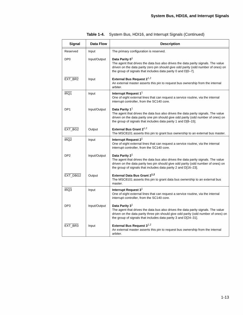
Communications Processor Module (CPM) Ports
1.7 Communications Processor Module (CPM) PortsThe MSC8101 CPM supports a subset of signals included in the MPC8260. The following sections describe the functionality of the signals in the MSC8101.
• The MSC8101 CPM includes the following set of communication controllers:• Two full-duplex Fast Serial Communications Controllers (FCCs) that support:
— Asynchronous Transfer Mode (ATM) through a UTOPIA 8 interface (FCC1 only)—The MSC8101 can operate as one of the following:
° UTOPIA slave device
° UTOPIA multi-PHY master device using direct polling for up to 4 PHY devices
° UTOPIA multi-PHY master device using multiplex polling that can address up to 31 PHY devices at addresses 0–30 (address 31 is reserved as a null port).
— IEEE 802.3/Fast Ethernet through a Media-Independent Interface (MII)— High-Level Data Link Control (HDLC) Protocol:
° Serial mode—Transfers data one bit at a time
° Nibble mode—Transfers data four bits at a time— Transparent mode serial operation
• One FCC that operates with the TSA only• Two Multi-Channel Controllers (MCCs) that together can handle up to 256 HDLC/transparent
channels at 64 Kbps each, multiplexed on up to four TDM interfaces• Two full-duplex serial communications controllers (SCCs) that support the following protocols:
— IEEE 802.3/Fast Ethernet through a Media-Independent Interface (MII)— HDLC Protocol:
° Serial mode—Transfers data one bit at a time
° Nibble mode—Transfers data four bits at a time— Synchronous Data Link Control (SDLC)— LocalTalk (HDLC-based local area network protocol)— Universal Asynchronous Receiver/Transmitter (UART)— Synchronous UART (1x clock mode)— Binary Synchronous (BISYNC) communication— Transparent mode serial operation
• Two additional SCCs that operate with the TSA only• Two full-duplex Serial Management Controllers (SMCs) that support the following protocols:
— General Circuit Interface (GCI)/Integrated Services Digital Network (ISDN) monitor and C/I channels (TSA only)
— UART— Transparent mode serial operation
• Serial Peripheral Interface (SPI) support for master or slave operation• Inter-Integrated Circuit (I2C) bus controller• Time-Slot Assigner (TSA) that supports multiplexing from any of the SCCs, FCCs, SMCs, and two
MCCs onto four time-division multiplexed (TDM) interfaces. The TSA uses two Serial Interfaces (SI1 and SI2). SI1 uses TDMA1 which supports both serial and nibble mode. SI2 does not support nibble mode and includes TDMB2, TDMC2, and TDMD2 which operate only in serial mode.
The individual sets of externals signals associated with a specific protocol and data transfer mode are multiplexed across any or all of the ports, as shown in Figure 1-2. The following sections provide detailed descriptions of the signals supported by Ports A–Port D.

1-19
Communications Processor Module (CPM) Ports
1.7.1 Port A Signals
Table 1-3. Port A Signals
NameDedicated I/O Data
DirectionDescriptionGeneral-
Purpose I/O
Peripheral Controller: Dedicated Signal
Protocol
PA31 FCC1: TXENBUTOPIA master
FCC1: TXENBUTOPIA slave
FCC1: COLMII
Output
Input
Input
FCC1: UTOPIA Master Transmit EnableIn the ATM UTOPIA interface supported by FCC1, TXENB is asserted by the MSC8101 (UTOPIA master PHY) when there is valid transmit cell data (TXD[0–7]).
FCC1: UTOPIA Slave Transmit EnableIn the ATM UTOPIA interface supported by FCC1, TXENB is asserted by an external UTOPIA master PHY when there is valid transmit cell data (TXD[0–7]).
FCC1: Media Independent Interface Collision Detect In the MII interface supported by FCC1, COL is asserted by an external fast Ethernet PHY.
PA30 FCC1: TXCLAVUTOPIA slave
FCC1: TXCLAVUTOPIA master, or
FCC1: TXCLAV0 UTOPIA master, Multi-PHY, direct polling
FCC1: RTSHDLC, Serial and Nibble
FCC1: CRSMII
Output
Input
Input
Output
Input
FCC1: UTOPIA Slave Transmit Cell AvailableIn the ATM UTOPIA interface supported by FCC1, TXCLAV is asserted by the MSC8101 (UTOPIA slave PHY) when the MSC8101 can accept one complete ATM cell.
FCC1: UTOPIA Master Transmit Cell Available In the ATM UTOPIA interface supported by FCC1, TXCLAV is asserted by an external UTOPIA slave PHY to indicate that it can accept one complete ATM cell.
FCC1: UTOPIA Master Transmit Cell Available Multi-PHY Direct PollingIn the ATM UTOPIA interface supported by FCC1, TXCLAV0 is asserted by an external UTOPIA slave PHY using direct polling to indicate that it can accept one complete ATM cell.
FCC1: Request To SendIn the standard modem interface signals supported by FCC1 (RTS, CTS, and CD). RTS is asynchronous with the data. RTS is typically used in conjunction with CD. The MSC8101 FCC1 transmitter requests the receiver to send data by asserting RTS low. The request is accepted when CTS is returned low.
FCC1: Media Independent Interface Carrier Sense In the MII interface supported by FCC1. CRS is asserted by an external fast Ethernet PHY. It indicates activity on the cable.

1-20
Communications Processor Module (CPM) Ports
PA29 FCC1: TXSOCUTOPIA master
FCC1: TXSOCUTOPIA slave
FCC1: TX_ERMII
Output
Input
Output
FCC1: UTOPIA Transmit Start of CellIn the ATM UTOPIA interface supported by FCC1. TXSOC is asserted by the MSC8101 (UTOPIA master PHY) when TXD[0–7] contains the first valid byte of the cell.
FCC1: UTOPIA Transmit Start of CellIn the ATM UTOPIA interface supported by FCC1. TXSOC is asserted by the external UTOPIA master PHY when TXD[0–7] contains the first valid byte of the cell.
FCC1: Media Independent Interface Transmit ErrorIn the MII interface supported by FCC1. TX_ER is asserted by the MSC8101 to force propagation of transmit errors.
PA28 FCC1: RXENBUTOPIA master
FCC1: RXENBUTOPIA slave
FCC1: TX_ENMII
Output
Input
Output
FCC1: UTOPIA Master Receive EnableIn the ATM UTOPIA interface supported by FCC1. (UTOPIA master) RXENB is asserted by the MSC8101 (UTOPIA master PHY) to indicate that RXD[0–7] and RXSOC are to be sampled at the end of the next cycle. RXD[0–7] and RXSOC are enabled only in cycles following those with RXENB asserted.
FCC1: UTOPIA Master Receive EnableIn the ATM UTOPIA interface supported by FCC1. (UTOPIA slave) RXENB is an input asserted by an external PHY to indicate that RXD[0–7] and RXSOC is to be sampled at the end of the next cycle. RXD[0–7] and RXSOC are enabled only in cycles following those with RXENB asserted.
FCC1: Media Independent Interface Transmit EnableIn the MII interface supported by FCC1. TX_EN is asserted by the MSC8101 when transmitting data.
PA27 FCC1: RXSOCUTOPIA master
FCC1: RXSOCUTOPIA slave
FCC1: RX_DVMII
Input
Output
Input
FCC1: UTOPIA Receive Start of CellAsserted by an external PHY when RXD[0–7] contains the first valid byte of the cell.
FCC1: UTOPIA Receive Start of CellAsserted by the MSC8101 (UTOPIA slave) for an external PHY when RXD[0–7] contains the first valid byte of the cell.
FCC1: Media Independent Interface Receive Data Valid In the MII interface supported by FCC1. RX_DV is an input asserted by an external fast Ethernet PHY. RX_DV indicates that valid data is being sent. The presence of carrier sense but not RX_DV indicates reception of broken packet headers, probably due to bad wiring or a bad circuit.
Table 1-3. Port A Signals (Continued)
NameDedicated I/O Data
DirectionDescriptionGeneral-
Purpose I/O
Peripheral Controller: Dedicated Signal
Protocol

1-21
Communications Processor Module (CPM) Ports
PA26 FCC1: RXCLAVUTOPIA slave
FCC1: RXCLAVUTOPIA master, or
RXCLAV0 UTOPIA master, Multi-PHY, direct polling
FCC1: RX_ERMII
Output
Input
Input
Input
FCC1: UTOPIA Slave Receive Cell AvailableIn the ATM UTOPIA interface supported by FCC1. RXCLAV is asserted by the MSC8101 (UTOPIA slave PHY) when one complete ATM cell is available for transfer.
FCC1: UTOPIA Master Receive Cell AvailableIn the ATM UTOPIA interface supported by FCC1. RXCLAV is asserted by an external PHY when one complete ATM cell is available for transfer.
FCC1: UTOPIA Master Receive Cell Available 0 Direct PollingIn the ATM UTOPIA interface supported by FCC1, RXCLAV0 is asserted by an external PHY when one complete ATM cell is available for transfer.
FCC1: Media Independent Interface Receive Error In the MII interface and supported by FCC1. RX_ER is asserted by an external fast Ethernet PHY. This signal indicates a receive error, which often indicates bad wiring.
PA25 FCC1: TXD0UTOPIA
SDMA: MSNUM0
Output
Output
FCC1: UTOPIA Transmit Data Bit 0In the ATM UTOPIA interface supported by FCC1. The MSC8101 outputs ATM cell octets (UTOPIA interface data) on TXD[0–7]. TXD7 is the most significant bit. TXD0 is the least significant bit. When no ATM data is available, idle cells are inserted. A cell is 53 bytes.
Module Serial Number Bit 0MSNUM[0–4] of is the sub-block code of the current peripheral controller using SDMA. MSNUM5 indicates which section, transmit (0) or receive (1), is active during the transfer.
PA24 FCC1: TXD1UTOPIA
SDMA: MSNUM1
Output
Output
FCC1: UTOPIA Transmit Data Bit 1In the ATM UTOPIA interface supported by FCC1. The MSC8101 outputs ATM cell octets (UTOPIA interface data) on TXD[0–7]. TXD7 is the most significant bit. TXD0 is the least significant bit. When no ATM data is available, idle cells are inserted. A cell is 53 bytes.
Module Serial Number Bit 1MSNUM[0–4] of is the sub-block code of the current peripheral controller using SDMA. MSNUM5 indicates which section, transmit (0) or receive (1), is active during the transfer.
PA23 FCC1: TXD2UTOPIA
Output FCC1: UTOPIA Transmit Data Bit 2TXD[0–7] is part of the ATM UTOPIA interface supported by FCC1. The MSC8101 outputs ATM cell octets (UTOPIA interface data) on TXD[0–7]. TXD7 is the most significant bit. TXD0 is the least significant bit. When no ATM data is available, idle cells are inserted. A cell is 53 bytes.
Table 1-3. Port A Signals (Continued)
NameDedicated I/O Data
DirectionDescriptionGeneral-
Purpose I/O
Peripheral Controller: Dedicated Signal
Protocol

1-22
Communications Processor Module (CPM) Ports
PA22 FCC1: TXD3UTOPIA
Output FCC1: UTOPIA Transmit Data Bit 3TXD[0–7] is part of the ATM UTOPIA interface supported by FCC1. The MSC8101 outputs ATM cell octets (UTOPIA interface data) on TXD[0–7]. TXD7 is the most significant bit. TXD0 is the least significant bit. When no ATM data is available, idle cells are inserted. A cell is 53 bytes.
PA21 FCC1: TXD4UTOPIA
FCC1: TXD3MII and HDLC nibble
Output
Output
FCC1: UTOPIA Transmit Data Bit 4TXD[0–7] is part of the ATM UTOPIA interface supported by FCC1. The MSC8101 outputs ATM cell octets (UTOPIA interface data) on TXD[0–7]. TXD7 is the most significant bit. TXD0 is the least significant bit. When no ATM data is available, idle cells are inserted. A cell is 53 bytes.
FCC1: MII and HDLC Nibble Transmit Data Bit 3TXD[3–0] supports MII and HDLC nibble modes in FCC1. TXD3 is the most significant bit. TXD0 is the least significant bit.
PA20 FCC1: TXD5UTOPIA
FCC1: TXD2MII and HDLC nibble
Output
Output
FCC1: UTOPIA Transmit Data Bit 5TXD[0–7] is part of the ATM UTOPIA interface supported by FCC1. The MSC8101 outputs ATM cell octets (UTOPIA interface data) on TXD[0–7]. TXD7 is the most significant bit. TXD0 is the least significant bit. When no ATM data is available, idle cells are inserted. A cell is 53 bytes.
FCC1: MII and HDLC Nibble Transmit Data Bit 2TXD[3–0] is supported by MII and HDLC nibble modes in FCC1. TXD3 is the most significant bit. TXD0 is the least significant bit.
PA19 FCC1: TXD6UTOPIA
FCC1: TXD1MII and HDLC nibble
Output
Output
FCC1: UTOPIA Transmit Data Bit 6TXD[0–7] is part of the ATM UTOPIA interface supported by FCC1. The MSC8101 outputs ATM cell octets (UTOPIA interface data) on TXD[0–7]. TXD7 is the most significant bit. TXD0 is the least significant bit. When no ATM data is available, idle cells are inserted. A cell is 53 bytes.
FCC1: MII and HDLC Nibble Transmit Data Bit 1 TXD[3–0] is supported by MII and HDLC transparent nibble modes in FCC1. TXD3 is the most significant bit. TXD0 is the least significant bit.
Table 1-3. Port A Signals (Continued)
NameDedicated I/O Data
DirectionDescriptionGeneral-
Purpose I/O
Peripheral Controller: Dedicated Signal
Protocol

1-23
Communications Processor Module (CPM) Ports
PA18 FCC1: TXD7UTOPIA
FCC1: TXD0MII and HDLC nibble
FCC1: TXDHDLC serial and transparent
Output
Output
Output
FCC1: UTOPIA Transmit Data Bit 7.TXD[0–7] is part of the ATM UTOPIA interface supported by FCC1. The MSC8101 outputs ATM cell octets (UTOPIA interface data) on TXD[0–7]. TXD7 is the most significant bit. TXD0 is the least significant bit. When no ATM data is available, idle cells are inserted. A cell is 53 bytes.
FCC1: MII and HDLC Nibble Transmit Data Bit 0 TXD[3–0] is supported by MII and HDLC nibble modes in FCC1. TXD3 is the most significant bit. TXD0 is the least significant bit.
FCC1: HDLC Serial and Transparent Transmit Data BitThe TXD serial bit is supported by HDLC serial and transparent modes in FCC1.
PA17 FCC1: RXD7UTOPIA
FCC1: RXD0MII and HDLC nibble
FCC1: RXDHDLC serial and transparent
Input
Input
Input
FCC1: UTOPIA Receive Data Bit 7.RXD[0–7] is part of the ATM UTOPIA interface supported by FCC1. The MSC8101 inputs ATM cell octets (UTOPIA interface data) on RXD[0–7]. RXD7 is the most significant bit. RXD0 is the least significant bit. When no ATM data is available, idle cells are inserted. A cell is 53 bytes. To support Multi-PHY configurations, RXD[0–7] is tri-stated, enabled only when RXENB is asserted.
FCC1: MII and HDLC Nibble Receive Data Bit 0 RXD[3–0] is supported by MII and HDLC nibble mode in FCC1. RXD3 is the most significant bit. RXD0 is the least significant bit.
FCC1: HDLC Serial and Transparent Receive Data BitThe RXD serial bit is supported by HDLC and transparent by FCC1.
PA16 FCC1: RXD6UTOPIA
FCC1: RXD1MII and HDLC nibble
Input
Input
FCC1: UTOPIA Receive Data Bit 6.RXD[0–7] is part of the ATM UTOPIA interface supported by FCC1. The MSC8101 inputs ATM cell octets (UTOPIA interface data) on RXD[0–7]. RXD7 is the most significant bit. RXD0 is the least significant bit. When no ATM data is available, idle cells are inserted. A cell is 53 bytes. To support Multi-PHY configurations, RXD[0–7] is tri-stated, enabled only when RXENB is asserted.
FCC1: MII and HDLC Nibble Receive Data Bit 1 RXD[3–0] is supported by MII and HDLC nibble mode in FCC1. RXD3 is the most significant bit. RXD0 is the least significant bit.
Table 1-3. Port A Signals (Continued)
NameDedicated I/O Data
DirectionDescriptionGeneral-
Purpose I/O
Peripheral Controller: Dedicated Signal
Protocol

1-24
Communications Processor Module (CPM) Ports
PA15 FCC1: RXD5UTOPIA
RXD2MII and HDLC nibble
Input
Input
FCC1: UTOPIA Receive Data Bit 5In the ATM UTOPIA interface supported by FCC1. The MSC8101 inputs ATM cell octets (UTOPIA interface data) on RXD[0–7]. RXD7 is the most significant bit. RXD0 is the least significant bit. When no ATM data is available, idle cells are inserted. A cell is 53 bytes. To support Multi-PHY configurations, RXD[0–7] is tri-stated, enabled only when RXENB is asserted.
FCC1: MII and HDLC Nibble Receive Data Bit 2 RXD[3–0] is supported by MII and HDLC nibble mode in FCC1. RXD3 is the most significant bit. RXD0 is the least significant bit.
PA14 FCC1: RXD4UTOPIA
FCC1: RXD3MII and HDLC nibble
Input
Input
FCC1: UTOPIA Receive Data Bit 4.In the ATM UTOPIA interface supported by FCC1. The MSC8101 inputs ATM cell octets (UTOPIA interface data) on RXD[0–7]. RXD7 is the most significant bit. RXD0 is the least significant bit. When no ATM data is available, idle cells are inserted. A cell is 53 bytes. To support Multi-PHY configurations, RXD[0–7] is tri-stated, enabled only when RXENB is asserted.
FCC1: MII and HDLC Nibble Receive Data Bit 3RXD[3–0] is supported by MII and HDLC nibble mode in FCC1. RXD3 is the most significant bit. RXD0 is the least significant bit.
PA13 FCC1: RXD3UTOPIA
SDMA: MSNUM2
Input
Output
FCC1: UTOPIA Receive Data Bit 3In the ATM UTOPIA interface supported by FCC1. The MSC8101 inputs ATM cell octets (UTOPIA interface data) on RXD[0–7]. RXD7 is the most significant bit. RXD0 is the least significant bit. A cell is 53 bytes. To support Multi-PHY configurations, RXD[0–7] is tri-stated, enabled only when RXENB is asserted.
Module Serial Number Bit 2MSNUM[0–4] is the sub-block code of the current peripheral controller using SDMA. MSNUM5 indicates which section, transmit (0) or receive (1), is active during the transfer.
PA12 FCC1: RXD2UTOPIA
SDMA: MSNUM3
Input
Output
FCC1: UTOPIA Receive Data Bit 2In the ATM UTOPIA interface supported by FCC1. The MSC8101 inputs ATM cell octets (UTOPIA interface data) on RXD[0–7]. RXD7 is the most significant bit. RXD0 is the least significant bit. A cell is 53 bytes. To support Multi-PHY configurations, RXD[0–7] is tri-stated, enabled only when RXENB is asserted.
Module Serial Number Bit 3MSNUM[0-4] of is the sub-block code of the current peripheral controller using SDMA. MSNUM5 indicates which section, transmit (0) or receive (1), is active during the transfer.
Table 1-3. Port A Signals (Continued)
NameDedicated I/O Data
DirectionDescriptionGeneral-
Purpose I/O
Peripheral Controller: Dedicated Signal
Protocol

1-25
Communications Processor Module (CPM) Ports
PA11 FCC1: RXD1UTOPIA
SDMA: MSNUM4
Input
Output
FCC1: UTOPIA RX Receive Data Bit 1In the ATM UTOPIA interface supported by FCC1. The MSC8101 inputs ATM cell octets (UTOPIA interface data) on RXD[0–7]. RXD7 is the most significant bit. RXD0 is the least significant bit. A cell is 53 bytes. To support Multi-PHY configurations, RXD[0–7] is tri-stated, enabled only when RXENB is asserted.
Module Serial Number Bit 4MSNUM[0–4] of is the sub-block code of the current peripheral controller using SDMA. MSNUM5 indicates which section, transmit (0) or receive (1) is active during the transfer.
PA10 FCC1: RXD0UTOPIA
SDMA: MSNUM5
Input
Output
FCC1: UTOPIA RX Receive Data Bit 0In the ATM UTOPIA interface supported by FCC1. The MSC8101 inputs ATM cell octets (UTOPIA interface data) on RXD[0–7]. RXD7 is the most significant bit. RXD0 is the least significant bit. A cell is 53 bytes. To support Multi-PHY configurations, RXD[0–7] is tri-stated, enabled only when RXENB is asserted.
Module Serial Number Bit 5MSNUM[0–4] of is the sub-block code of the current peripheral controller using SDMA. MSNUM5 indicates which section, transmit (0) or receive (1), is active during the transfer.
PA9 SMC2: SMTXD
SI1 TDMA1: L1TXD0TDM nibble
Output
Output
SMC2: Serial Management Transmit DataSupported by SMC2. The SMC interface consists of SMTXD, SMRXD, SMSYN, and a clock. Not all signals are used for all applications. SMCs are full-duplex ports that supports three protocols or modes: UART, transparent, or general-circuit interface (GCI). See also PC15.
Time-Division Multiplexing A1: Layer 1 Transmit Data Bit 0In the TDMA1 interface supported by SI1. L1TXD3 is the most significant bit. L1TXD0 is the least significant bit in nibble mode. TDMA1 transmits nibble data out L1TXD[0–3].
Table 1-3. Port A Signals (Continued)
NameDedicated I/O Data
DirectionDescriptionGeneral-
Purpose I/O
Peripheral Controller: Dedicated Signal
Protocol

1-26
Communications Processor Module (CPM) Ports
PA8 SMC2: SMRXD
SI1 TDMA1: L1RXD0TDM nibble
SI1 TDMA1: L1RXDTDM serial
Input
Input
Input
SMC2: Serial Management Receive DataSupported by SMC2. The SMC interface consists of SMTXD, SMRXD, SMSYN, and a clock. Not all signals are used for all applications. SMCs are full-duplex ports that supports three protocols or modes: UART, transparent, or general-circuit interface (GCI).
Time-Division Multiplexing A1: Layer 1 Nibble Receive Data Bit 0In the TDMA1 interface supported by SI1. L1RXD3 is the most significant bit. L1RXD0 is the least significant bit in nibble mode. TDMA1 receives nibble data from L1RXD[0–3].
Time-Division Multiplexing A1: Layer 1 Serial Receive DataIn the TDMA1 interface supported by SI1. TDMA1 receives serial data from L1RXD.
PA7 SMC2: SMSYN
SI1 TDMA1: L1TSYNC/GRANTTDM nibble and TDM serial
Input
Input
SMC2: Serial Management SynchronizationThe SMC interface consists of SMTXD, SMRXD, SMSYN, and a clock. Not all signals are used for all applications. SMCs are full-duplex ports that supports three protocols or modes: UART, transparent, or general-circuit interface (GCI).
Time-Division Multiplexing A1: Layer 1 Transmit Synchronization/GrantIn the TDMA1 interface supported by SI1, this is the synchronizing signal for the transmit channel. If Grant Mode is enabled this bit is sampled as the Grant bit for IDL mode access for the D channel. See the Serial Interface with Time-Slot Assigner chapter in the MSC8101 Technical Reference manual.
PA6 SI1 TDMA1: L1RSYNCTDM nibble and TDM serial
Input Time-Division Multiplexing A1: Layer 1 Receive Synchronization.In the TDMA1 interface supported by SI1, this is the synchronizing signal for the receive channel.
Table 1-3. Port A Signals (Continued)
NameDedicated I/O Data
DirectionDescriptionGeneral-
Purpose I/O
Peripheral Controller: Dedicated Signal
Protocol

1-27
Communications Processor Module (CPM) Ports
1.7.2 Port B Signals
Table 1-4. Port B Signals
NameDedicated I/O Data
DirectionDescriptionGeneral-
Purpose I/O
Peripheral Controller: Dedicated I/O
Protocol
PB31 FCC2: TX_ERMII
SCC2: RXD
SI2 TDMB2: L1TXDTDM serial
Output
Input
Output
FCC2: Media Independent Interface Transmit ErrorIn the MII interface supported by FCC2. TX_ER is asserted by the MSC8101 to force propagation of transmit errors.
SCC2: Receive DataSupported by SCC2. SCC2 receives serial data from RXD.
Time-Division Multiplexing B2: Layer 1 Transmit DataIn the TDMB2 interface supported by SI2. L1TXD supports serial mode. TDMB2 transmits serial data out of L1TXD.
PB30 SCC2: TXD
FCC2: RX_DVMII
SI2 TDMB2: L1RXDTDM serial
Output
Input
Input
SCC2: Transmit Data. Supported by SCC2. SCC2 transmits serial data out of TXD.
FCC2: Media Independent Interface Receive Data Valid In the MII interface supported by FCC2, RX_DV is asserted by an external fast Ethernet PHY. RX_DV indicates that valid data is being sent. The presence of carrier sense, but not RX_DV, indicates reception of broken packet headers, probably due to bad wiring or a bad circuit.
Time-Division Multiplexing B2: Layer 1 Receive DataIn the TDMB2 interface supported by SI2. L1RXD supports serial mode. TDMB2 receives serial data from L1RXD.
PB29 FCC2: TX_ENMII
SI2 TDMB2: L1RSYNCTDM serial
Output
Input
FCC2: Media Independent Interface Transmit EnableIn the MII interface supported by FCC2. TX_EN is asserted by the MSC8101 when transmitting data.
Time-Division Multiplexing B2: Layer 1 Receive SynchronizationIn the TDMB2 interface supported by SI2, this is the synchronizing signal for the receive channel.

1-28
Communications Processor Module (CPM) Ports
PB28 FCC2: RTSHDLC serial, HDLC nibble, and transparent
FCC2: RX_ERMII
SCC2: RTS, TENA
SI2 TDMB2: L1TSYNC/GRANTTDM serial
Output
Input
Output
Input
FCC2: Request to SendOne of the standard modem interface signals supported by FCC2 (RTS, CTS, and CD). RTS is asynchronous with the data. RTS is typically used in conjunction with CD. The MSC8101 FCC2 transmitter requests the receiver to send data by asserting RTS low. The request is accepted when CTS is returned low.
FCC2: Media Independent Interface Receive ErrorIn the MII interface supported by FCC2, RX_ER is asserted by an external fast Ethernet PHY. This signal indicates a receive error, which often indicates bad wiring.
SCC2: Request to Send, Transmit EnableTypically used in conjunction with CD supported by SCC2. The MSC8101 SCC2 transmitter requests the receiver to send data by asserting RTS low. The request is accepted when CTS is returned low. TENA is the signal used in Ethernet mode.
Time-Division Multiplexing B2: Layer 1 Transmit SynchronizationIn the TDMB2 interface supported by SI2, this is the synchronizing signal for the transmit channel. If Grant Mode is enabled this bit is sampled as the Grant bit for IDL mode access for the D channel. See the Serial Interface with Time-Slot Assigner chapter in the MSC8101 Technical Reference manual.
PB27 FCC2: COLMII
SI2 TDMC2: L1TXDTDM serial
Input
Output
FCC2: Media Independent Interface Collision DetectIn the MII interface supported by FCC2. COL is asserted by an external fast Ethernet PHY.
Time-Division Multiplexing C2: Layer 1 Transmit DataIn the TDMC2 interface supported by SI2. L1TXD supports serial mode. TDMC2 transmits serial data out of L1TXD.
PB26 FCC2: CRSMII
SI2 TDMC2: L1RXDTDM serial
Input
Input
FCC2: Media Independent Interface Carrier Sense InputIn the MII interface, CRS is asserted by an external fast Ethernet PHY. This signal indicates activity on the cable.
Time-Division Multiplexing C2: Layer 1 Receive DataIn the TDMC2 interface supported by SI2. L1RXD supports serial mode. TDMC2 receives serial data from L1RXD.
Table 1-4. Port B Signals (Continued)
NameDedicated I/O Data
DirectionDescriptionGeneral-
Purpose I/O
Peripheral Controller: Dedicated I/O
Protocol

1-29
Communications Processor Module (CPM) Ports
PB25 FCC2: TXD3MII and HDLC nibble
SI1 TDMA1: L1TXD3TDM nibble
SI2 TDMC2: L1TSYNC/GRANTTDM serial
Output
Output
Input
FCC2: MII and HDLC Nibble Transmit Data Bit 3Supported by MII and HDLC nibble mode in FCC2. TXD3 is the most significant bit. TXD0 is the least significant bit.
Time-Division Multiplexing A1: Nibble Layer 1 Transmit Data Bit 3TDMA1 transmits nibble data out of L1TXD[0–3]. L1TXD3 is the most significant bit and L1TXD0 is the least significant bit in nibble mode.
Time-Division Multiplexing C2: Layer 1 Transmit SynchronizationIn the TDMC2 interface supported by SI2, this is the synchronizing signal for the transmit channel. If Grant Mode is enabled, this bit is sampled as the Grant bit for IDL mode access for the D channel. See the Serial Interface with Time-Slot Assigner chapter in the MSC8101 Technical Reference manual.
PB24 FCC2: TXD2 MII and HDLC nibble
SI1 TDMA1: L1RXD3nibble
SI2 TDMC2: L1RSYNCserial
Output
Input
Input
FCC2: MII and HDLC Nibble: Transmit Data Bit 2 Supported by MII and HDLC nibble mode in FCC2. TXD3 is the most significant bit. TXD0 is the least significant bit.
Time-Division Multiplexing A1: Nibble Layer 1 Receive Data Bit 3TDMA1 receives nibble data into L1RXD[0–3]. L1RXD3 is the most significant bit and L1RXD0 is the least significant bit in nibble mode.
Time-Division Multiplexing C2: Layer 1 Receive SynchronizationIn the TDMC2 interface supported by SI2, this is the synchronizing signal for the receive channel.
PB23 FCC2: TXD1MII and HDLC nibble
SI1 TDMA1: L1RXD2TDM nibble
SI2 TDMD2: L1TXDTDM serial
Output
Input
Output
FCC2: MII and HDLC Nibble: Transmit Data Bit 1Supported by MII and HDLC nibble mode in FCC2. TXD3 is the most significant bit. TXD0 is the least significant bit.
Time-Division Multiplexing A1: Nibble Layer 1 Receive Data Bit 2In the TDMA1 interface supported by SI1. TDMA1 supports bit and nibble modes. L1RXD3 is the most significant bit. L1RXD0 is the least significant bit in nibble mode. TDMA1 receives nibble data from L1RXD[0–3].
Time-Division Multiplexing D2: Layer 1 Transmit DataIn the TDMD2 interface supported by SI2. L1TXD supports serial mode. TDMA1 transmits serial data out of L1TXD.
Table 1-4. Port B Signals (Continued)
NameDedicated I/O Data
DirectionDescriptionGeneral-
Purpose I/O
Peripheral Controller: Dedicated I/O
Protocol

1-30
Communications Processor Module (CPM) Ports
PB22 FCC2: TXD0MII and HDLC nibble
FCC2: TXDHDLC serial and transparent
SI1 TDMA1: L1RXD1TDM nibble
SI2 TDMD2: L1RXDTDM serial
Output
Output
Input
Input
FCC2: MII and HDLC Nibble Transmit Data Bit 0TXD[0–3] is supported by MII and HDLC nibble mode in FCC2. TXD3 is the most significant bit. TXD0 is the least significant bit.
FCC2: HDLC Serial and Transparent Transmit DataTXD is supported by HDLC serial mode and transparent mode in FCC2.
Time-Division Multiplexing A1: Nibble Layer 1 Receive Data Bit 1In the TDMA1 interface supported by SI1. TDMA1 supports bit and nibble modes. L1RXD3 is the most significant bit. L1RXD0 is the least significant bit in nibble mode. TDMA1 receives nibble data from L1RXD[0–3].
Time-Division Multiplexing D2: Layer 1 Receive DataIn the TDMD2 interface supported by SI2. TDMD2 supports serial mode. TDMD2 receives serial data from L1RXD.
PB21 FCC2: RXD0MII and HDLC nibble
FCC2: RXDHDLC serial and transparent
SI1 TDMA1: L1TXD2TDM nibble
SI2 TDMD2: L1TSYNC/GRANTTDM serial
Input
Input
Output
Input
FCC2: MII and HDLC Nibble Receive Data Bit 0 RXD[0–3] is supported by MII and HDLC nibble mode in FCC2. RXD3 is the most significant bit. RXD0 is the least significant bit.
FCC2: HDLC Serial and Transparent Receive DataSupported by HDLC serial mode and transparent mode in FCC2.
Time-Division Multiplexing A1: Nibble Layer 1 Transmit Data Bit 2In the TDMA1 interface supported by SI1. TDMA1 supports bit and nibble modes. L1TXD3 is the most significant bit. L1TXD0 is the least significant bit in nibble mode. TDMA1 transmits nibble data out of L1TXD[0–3].
Time-Division Multiplexing D2: Layer 1 Transmit Synchronize DataIn the TDMD2 interface supported by SI2, this is the synchronizing signal for the transmit channel. If Grant Mode is enabled this bit is sampled as the Grant bit for IDL mode access for the D channel. See the Serial Interface with Time-Slot Assigner chapter in the MSC8101 Technical Reference manual.
Table 1-4. Port B Signals (Continued)
NameDedicated I/O Data
DirectionDescriptionGeneral-
Purpose I/O
Peripheral Controller: Dedicated I/O
Protocol

1-31
Communications Processor Module (CPM) Ports
PB20 FCC2: RXD1MII and HDLC nibble
SI1 TDMA1: L1TXD1TDM nibble
SI2 TDMD2: L1RSYNCTDM serial
Input
Output
Input
FCC2: MII and HDLC Nibble: Receive Data Bit 1RXD[0–3] is supported by MII and HDLC nibble mode in FCC2. RXD3 is the most significant bit. RXD0 is the least significant bit.
Time-Division Multiplexing A1: Nibble Layer 1 Transmit Data Bit 1In the TDMA1 interface supported by SI1. TDMA1 supports bit and nibble modes. L1TXD3 is the most significant bit. L1TXD0 is the least significant bit in nibble mode. TDMA1 transmits nibble data out of L1TXD[0–3].
Time-Division Multiplexing D2: Layer 1 Receive Synchronize DataIn the TDMD2 interface supported by SI2, this is the synchronizing signal for the receive channel.
PB19 FCC2: RXD2 MII and HDLC nibble
I2C: SDA
Input
Input/ Output
FCC2: MII and HDLC Nibble Receive Data Bit 2RXD[0–3] is supported by MII and HDLC nibble mode in FCC2. RXD3 is the most significant bit. RXD0 is the least significant bit.
I2C: Inter-Integrated Circuit Serial DataThe I2C interface comprises two signals: serial data (SDA) and serial clock (SDA). The I2C controller uses a synchronous, multimaster bus that can connect several integrated circuits on a board. Clock rates run up to 520 kHz@25 MHz system clock.
PB18 FCC2: RXD3MII and HDLC nibble
I2C: SCL
Input
Input/ Output
FCC2: MII and HDLC Nibble Receive Data Bit 3RXD[0–3] is supported by MII and HDLC nibble mode in FCC2. RXD3 is the most significant bit. RXD0 is the least significant bit.
I2C: Inter-Integrated Circuit Serial ClockThe I2C interface comprises two signals: serial data (SDA) and serial clock (SDA). The I2C controller uses a synchronous, multimaster bus that can connect several integrated circuits on a board. Clock rates run up to 520 kHz@25 MHz system clock.
Table 1-4. Port B Signals (Continued)
NameDedicated I/O Data
DirectionDescriptionGeneral-
Purpose I/O
Peripheral Controller: Dedicated I/O
Protocol

1-32
Communications Processor Module (CPM) Ports
1.7.3 Port C Signals
Table 1-5. Port C Signals
NameDedicated I/O Data
DirectionDescriptionGeneral-
Purpose I/O
Peripheral Controller: Dedicated I/O
Protocol
PC31 BRG1O
CLK1
TIMER1/2: TGATE1
Output
Input
Input
Baud-Rate Generator 1 OutputThe CPM supports up to 8 BRGs. The BRGs can be used internally by the bank-of-clocks selection logic and/or provide an output to one of the 8 BRG pins. BRG1O can be the internal input to the SIU timers. When CLK5 is selected (see PC27 below), it is the source for BRG1O which is the default input for the SIU timers. See the System Interface Unit (SIU) chapter in the MSC8101 Technical Reference manual for additional information. If CLK5 is not enabled, BRG1O uses an internal input. If TMCLK is enabled (see PC26 below), the BRG1O input to the SIU timers is disabled.
Clock 1The CPM supports up to 10 clock input pins. The clocks are sent to the bank-of-clocks selection logic, where they can be routed to the controllers.
Timer 1/2: Timer Gate 1The timers can be gated/restarted by an external gate signal. There are two gate signals: TGATE1 controls timer 1 and/or 2 and TGATE2 controls timer 3 and/or 4.
PC30 BRG2O
CLK2
Timer1: TOUT1
EXT1
Output
Input
Output
Input
Baud-Rate Generator 2 OutputThe CPM supports up to 8 BRGs. The BRGs can be used internally by the bank-of-clocks selection logic and/or provide an output to one of the 8 BRG pins.
Clock 2The CPM supports up to 10 clock input pins. The clocks are sent to the bank-of-clocks selection logic, where they can be routed to the controllers.
Timer 1: Timer Out 1The timers (Timer[1–4]) can output a signal on a timer output (TOUT[1–4]) when the reference value is reached. This signal can be an active-low pulse or a toggle of the current output. The output can also connect internally to the input of another timer, resulting in a 32-bit timer.
External Request 1External request input line 1 asserts an internal request to the CPM processor. The signal can be programmed as level- or edge-sensitive, and also has programmable priority. Refer to the RISC Controller Configuration Register (RCCR) description in the Chapter 17 of the MSC8101 Reference Manual for programming information. There are no current microcode applications for this request line. It is reserved for future development.

1-33
Communications Processor Module (CPM) Ports
PC29 BRG3O
CLK3
TIN2
SCC1: CTS, CLSN
Output
Input
Input
Input
Baud-Rate Generator 3 OutputThe CPM supports up to 8 BRGs. The BRGs can be used internally by the bank-of-clocks selection logic and/or provide an output to one of the 8 BRG pins.
Clock 3The CPM supports up to 10 clock input pins. The clocks are sent to the bank-of-clocks selection logic, where they can be routed to the controllers.
Timer Input 2A timer can have one of the following sources: another timer, system clock, system clock divided by 16 or a timer input. The CPM supports up to 4 timer inputs. The timer inputs can be captured on the rising, falling or both edges.
SCC1: Clear to Send, CollisionTypically used in conjunction with RTS. The MSC8101 SCC1 transmitter sends out a request to send data signal (RTS). The request is accepted when CTS is returned low. CLSN is the signal used in Ethernet mode. See also PC15.
PC28 BRG4O
CLK4
TIN1
Timer2: TOUT2
SCC2: CTS, CLSN
Output
Input
Input
Output
Input
Baud-Rate Generator 4 OutputThe CPM supports up to 8 BRGs. The BRGs can be used internally by the bank-of-clocks selection logic and/or provide an output to one of the 8 BRG pins.
Clock 4The CPM supports up to 10 clock input pins. The clocks are sent to the bank-of-clocks selection logic, where they can be routed to the controllers.
Timer Input 1A timer can have one of the following sources: another timer, system clock, system clock divided by 16 or a timer input. The CPM supports up to 4 timer inputs. The timer inputs can be captured on the rising, falling or both edges.
Timer 2: Timer Output 2The timers (Timer[1–4]) can output a signal on a timer output (TOUT[1–4]) when the reference value is reached. This signal can be an active-low pulse or a toggle of the current output. The output can also be connected internally to the input of another timer, resulting in a 32-bit timer.
SCC2: Clear to Send, CollisionTypically used in conjunction with RTS. The MSC8101 SCC2 transmitter sends out a request to send data signal (RTS). The request is accepted when CTS is returned low. CLSN is the signal used in Ethernet mode. See also PC13.
Table 1-5. Port C Signals (Continued)
NameDedicated I/O Data
DirectionDescriptionGeneral-
Purpose I/O
Peripheral Controller: Dedicated I/O
Protocol
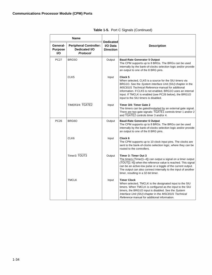
1-34
Communications Processor Module (CPM) Ports
PC27 BRG5O
CLK5
TIMER3/4: TGATE2
Output
Input
Input
Baud-Rate Generator 5 OutputThe CPM supports up to 8 BRGs. The BRGs can be used internally by the bank-of-clocks selection logic and/or provide an output to one of the 8 BRG pins.
Clock 5When selected, CLK5 is a source for the SIU timers via BRG1O. See the System Interface Unit (SIU) chapter in the MSC8101 Technical Reference manual for additional information. If CLK5 is not enabled, BRG1O uses an internal input. If TMCLK is enabled (see PC26 below), the BRG1O input to the SIU timers is disabled.
Timer 3/4: Timer Gate 2The timers can be gated/restarted by an external gate signal. There are two gate signals: TGATE1 controls timer 1 and/or 2 and TGATE2 controls timer 3 and/or 4.
PC26 BRG6O
CLK6
Timer3: TOUT3
TMCLK
Output
Input
Output
Input
Baud-Rate Generator 6 OutputThe CPM supports up to 8 BRGs. The BRGs can be used internally by the bank-of-clocks selection logic and/or provide an output to one of the 8 BRG pins.
Clock 6The CPM supports up to 10 clock input pins. The clocks are sent to the bank-of-clocks selection logic, where they can be routed to the controllers.
Timer 3: Timer Out 3The timers (Timer[1–4]) can output a signal on a timer output (TOUT[1–4]) when the reference value is reached. This signal can be an active-low pulse or a toggle of the current output. The output can also connect internally to the input of another timer, resulting in a 32-bit timer.
Timer ClockWhen selected, TMCLK is the designated input to the SIU timers. When TMCLK is configured as the input to the SIU timers, the BRG1O input is disabled. See the System Interface Unit (SIU) chapter in the MSC8101 Technical Reference manual for additional information.
Table 1-5. Port C Signals (Continued)
NameDedicated I/O Data
DirectionDescriptionGeneral-
Purpose I/O
Peripheral Controller: Dedicated I/O
Protocol

1-35
Communications Processor Module (CPM) Ports
PC25 BRG7O
CLK7
TIN4
DMA: DACK2
Output
Input
Input
Output
Baud-Rate Generator 7 OutputThe CPM supports up to 8 BRGs. The BRGs can be used internally by the bank-of-clocks selection logic and/or provide an output to one of the 8 BRG pins.
Clock 7The CPM supports up to 10 clock input pins. The clocks are sent to the bank-of-clocks selection logic, where they can be routed to the controllers.
Timer Input 4A timer can have one of the following sources: another timer, system clock, system clock divided by 16 or a timer input. The CPM supports up to 4 timer inputs. The timer inputs can be captured on the rising, falling or both edges.
DMA: Data Acknowledge 2DACK2, DREQ2, DRACK2 and DONE2 belong to the SIU DMA. DONE2 and DRACK2 are signals on the same pin and therefore cannot be used simultaneously. There are two sets of DMA pins associated with the PIO ports.
PC24 BRG8O
CLK8
TIN3
Timer4: TOUT4
DMA: DREQ2
Output
Input
Input
Output
Input
Baud-Rate Generator 8 OutputThe CPM supports up to 8 BRGs. The BRGs can be used internally by the bank-of-clocks selection logic and/or provide an output to one of the 8 BRG pins.
Clock 8The CPM supports up to 10 clock input pins. The clocks are sent to the bank-of-clocks selection logic, where they can be routed to the controllers.
Timer Input 3A timer can have one of the following sources: another timer, system clock, system clock divided by 16, or a timer input. The CPM supports up to four timer inputs. The timer inputs can be captured on the rising, falling, or both edges.
Timer 4: Timer Out 4The timers (Timer1–4]) can output a signal on a timer output (TOUT[1–4]) when the reference value is reached. This signal can be an active-low pulse or a toggle of the current output. The output can also be connected internally to the input of another timer, resulting in a 32-bit timer.
DMA: Data Request 2DACK2, DREQ2, DRACK2, and DONE2 belong to the SIU DMA. DONE2 and DRACK2 are signals on the same pin and therefore cannot be used simultaneously. There are two sets of DMA pins associated with the PIO ports.
Table 1-5. Port C Signals (Continued)
NameDedicated I/O Data
DirectionDescriptionGeneral-
Purpose I/O
Peripheral Controller: Dedicated I/O
Protocol

1-36
Communications Processor Module (CPM) Ports
PC23 CLK9
DMA: DACK1
EXT2
Input
Output
Input
Clock 9 The CPM supports up to 10 clock input pins. The clocks are sent to the bank-of-clocks selection logic, where they can be routed to the controllers.
DMA: Data Acknowledge 1DACK1, DREQ1, DRACK1, and DONE1 belong to the SIU DMA. DONE1 and DRACK1 are signals on the same pin and therefore cannot be used simultaneously. There are two sets of DMA pins associated with the PIO ports.
External Request 2External request input line 2 asserts an internal request to the CPM processor. The signal can be programmed as level- or edge-sensitive, and also has programmable priority. Refer to the RISC Controller Configuration Register (RCCR) description in the Chapter 17 of the MSC8101 Reference Manual for programming information. There are no current microcode applications for this request line. It is reserved for future development.
PC22 SI1: L1ST1
CLK10
DMA: DREQ1
Output
Input
Input/ Output
Serial Interface 1: Layer 1 Strobe 1In the time-slot assigner supported by SI1. The MSC8101 time-slot assigner supports up to four strobe outputs that can be asserted on a bit or byte basis. The strobe outputs are useful for interfacing to other devices that do not support the multiplexed interface or for enabling/disabling three-state I/O buffers in a multiple-transmitter architecture. These strobes can also generate output wave forms for such applications as stepper-motor control.
Clock 10The CPM supports up to 10 clock input pins. The clocks are sent to the bank-of-clocks selection logic, where they can be routed to the controllers.
DMA: Request 1DACK1, DREQ1, DRACK1, and DONE1 belong to the SIU DMA. DONE1 and DRACK1 are signals on the same pin and therefore cannot be used simultaneously. There are two sets of DMA pins associated with the PIO ports.
Table 1-5. Port C Signals (Continued)
NameDedicated I/O Data
DirectionDescriptionGeneral-
Purpose I/O
Peripheral Controller: Dedicated I/O
Protocol

1-37
Communications Processor Module (CPM) Ports
PC15 SMC2: SMTXD
SCC1: CTS/CLSN
FCC1: TXADDR0UTOPIA master
FCC1: TXADDR0UTOPIA slave
Output
Input
Output
Input
SMC2: Serial Management Transmit DataSupported by SMC2. The SMC interface consists of SMTXD, SMRXD, SMSYN, and a clock. Not all signals are used for all applications. SMCs are full-duplex ports that support three protocols or modes: UART, transparent, or general-circuit interface (GCI). See also PA9.
SCC1: Clear To Send, CollisionTypically used in conjunction with RTS. The MSC8101 SCC1 transmitter sends out a request to send data signal (RTS). The request is accepted when CTS is returned low. CLSN is the signal used in Ethernet mode. See also PC29.
FCC1: UTOPIA Master Transmit Address Bit 0In the ATM UTOPIA master interface supported by FCC1, this is transmit address bit 0.
FCC1: UTOPIA Slave Transmit Address Bit 0In the ATM UTOPIA slave interface supported by FCC1, this is transmit address bit 0.
PC14 SI1: L1ST2
SCC1: CD, RENA
FCC1: RXADDR0UTOPIA master
FCC1: RXADDR0UTOPIA slave
Output
Input
Output
Input
Serial Interface 1: Layer 1 Strobe 2In the time-slot assigner supported by SI1. The MSC8101 time-slot assigner supports up to four strobe outputs that can be asserted on a bit or byte basis. The strobe outputs are useful for interfacing to other devices that do not support the multiplexed interface or for enabling/disabling three-state I/O buffers in a multiple-transmitter architecture. These strobes can also be generate output wave forms for such applications as stepper-motor control.
SCC1: Carrier Detect, Receive EnableTypically used in conjunction with RTS supported by SCC1. The MSC8101 SCC1 transmitter requests the receiver to send data by asserting RTS low. The request is accepted when CTS is returned low.
FCC1: UTOPIA Multi-PHY Master Receive Address Bit 0In the ATM UTOPIA master interface supported by FCC1, this is receive address bit 0.
FCC1: UTOPIA Multi-PHY Slave Receive Address Bit 0In the ATM UTOPIA slave interface supported by FCC1, this is receive address bit 0.
Table 1-5. Port C Signals (Continued)
NameDedicated I/O Data
DirectionDescriptionGeneral-
Purpose I/O
Peripheral Controller: Dedicated I/O
Protocol

1-38
Communications Processor Module (CPM) Ports
PC13 SI1: L1ST4
SCC2: CTS,CLSN
FCC1:TXADDR1UTOPIA master
FCC1: TXADDR1UTOPIA slave
Output
Input
Output
Input
Serial Interface 1: Layer 1 Strobe 4In the time-slot assigner supported by SI1. The MSC8101 time-slot assigner supports up to four strobe outputs that can be asserted on a bit or byte basis. The strobe outputs are useful for interfacing to other devices that do not support the multiplexed interface or for enabling/disabling three-state I/O buffers in a multiple-transmitter architecture. These strobes can also generate output wave forms for such applications as stepper-motor control.
SCC2: Clear to Send, CollisionTypically used in conjunction with RTS. The MSC8101 SCC2 transmitter sends out a request to send data signal (RTS). The request is accepted when CTS is returned low. CLSN is the signal used in Ethernet mode. See also PC28.
FCC1: UTOPIA Multi-PHY Master Transmit Address Bit 1In the ATM UTOPIA master interface supported by FCC1, this is transmit address bit 1.
FCC1: UTOPIA Multi-PHY Slave Transmit Address Bit 1In the ATM UTOPIA slave interface supported by FCC1, this is transmit address bit 1.
PC12 SI1: L1ST3
SCC2: CD, RENA
FCC1: RXADDR1UTOPIA master
FCC1: RXADDR1UTOPIA slave
Output
Input
Output
Input
Serial Interface 1: Layer 1 Strobe 3In the time-slot assigner supported by SI1. The MSC8101 time-slot assigner supports up to four strobe outputs that can be asserted on a bit or byte basis. The strobe outputs are useful for interfacing to other devices that do not support the multiplexed interface or for enabling/disabling three-state I/O buffers in a multiple-transmitter architecture. These strobes can also generate output wave forms for such applications as stepper-motor control.
SCC2: Carrier Detect, Request EnableTypically used in conjunction with RTS supported by SCC2. The MSC8101 SCC2 transmitter requests to the receiver that it sends data by asserting RTS low. The request is accepted when CTS is returned low.
FCC1: UTOPIA Multi-PHY Master Receive Address Bit 1In the ATM UTOPIA master interface supported by FCC1, this is receive address bit 1.
FCC1: UTOPIA Multi-PHY Slave Receive Address Bit 1In the ATM UTOPIA slave interface supported by FCC1, this is receive address bit 1.
Table 1-5. Port C Signals (Continued)
NameDedicated I/O Data
DirectionDescriptionGeneral-
Purpose I/O
Peripheral Controller: Dedicated I/O
Protocol

1-39
Communications Processor Module (CPM) Ports
PC7 SI2: L1ST1
FCC1: CTSHDLC serial, HDLC nibble,and transparent
FCC1: TXADDR2UTOPIA master
FCC1: TXADDR2UTOPIA slave
FCC1: TXCLAV1 UTOPIA multi-PHY master, direct polling
Output
Input
Output
Input
Input
Serial Interface 2: Strobe 1In the time-slot assigner supported by SI2. The MSC8101 time-slot assigner supports up to four strobe outputs that can be asserted on a bit or byte basis. The strobe outputs are useful for interfacing to other devices that do not support the multiplexed interface or for enabling/disabling three-state I/O buffers in a multiple-transmitter architecture. These strobes can also generate output wave forms for such applications as stepper-motor control.
FCC1: Clear To SendIn the standard modem interface signals supported by FCC1 (RTS, CTS, and CD). CTS is asynchronous with the data.
FCC1: UTOPIA Multi-PHY Master Transmit Address Bit 2 In the ATM UTOPIA master interface supported by FCC1, this is transmit address bit 2.
FCC1: UTOPIA Multi-PHY Slave Transmit Address Bit 2 In the ATM UTOPIA slave interface supported by FCC1 using multiplexed polling, this is transmit address bit 2.
FCC1: UTOPIA Multi-PHY Master Transmit Cell Available 1 Direct PollingIn the ATM UTOPIA master interface supported by FCC1 using direct polling, TXCLAV1 is asserted by an external UTOPIA slave PHY to indicate that it can accept one complete ATM cell.
Table 1-5. Port C Signals (Continued)
NameDedicated I/O Data
DirectionDescriptionGeneral-
Purpose I/O
Peripheral Controller: Dedicated I/O
Protocol

1-40
Communications Processor Module (CPM) Ports
PC6 SI2: L1ST2
FCC1: CDHDLC serial, HDLC nibble,and transparent
FCC1: RXADDR2UTOPIA master
FCC1: RXADDR2UTOPIA slave
FCC1: RXCLAV1 UTOPIA multi-PHY master, direct polling
Output
Input
Output
Input
Input
Serial Interface 2: Layer 1 Strobe 2In the time-slot assigner supported by SI2. The MSC8101 time-slot assigner supports up to four strobe outputs that can be asserted on a bit or byte basis. The strobe outputs are useful for interfacing to other devices that do not support the multiplexed interface or for enabling/disabling three-state I/O buffers in a multiple-transmitter architecture. These strobes can also generate output wave forms for such applications as stepper-motor control.
FCC1: Carrier DetectIn the standard modem interface signals supported by FCC1 (RTS, CTS, and CD). CD is an input asynchronous with the data.
FCC1: UTOPIA Multi-PHY Master Receive Address Bit 2In the ATM UTOPIA master interface supported by FCC1, this is receive address bit 2.
FCC1: UTOPIA Slave Receive Address Bit 2In the ATM UTOPIA slave interface supported by FCC1 using multiplexed polling, this is receive address bit 2.
FCC1: UTOPIA Multi-PHY Master Receive Cell Available 1 Direct PollingIn the ATM UTOPIA master interface supported by FCC1 using direct polling, RXCLAV1 is asserted by an external PHY when one complete ATM cell is available for transfer.
PC5 SMC1: SMTXD
SI2: L1ST3
FCC2: CTSHDLC serial, HDLC nibble,and transparent
Output
Output
Input
SMC1: Transmit DataSupported by SMC1. The SMC interface consists of SMTXD, SMRXD, SMSYN, and a clock. Not all signals are used for all applications. SMCs are full-duplex ports that supports three protocols or modes: UART, transparent, or general-circuit interface (GCI).
Serial Interface 2: Layer 1 Strobe 3In the time-slot assigner supported by SI2. The MSC8101 time-slot assigner supports up to four strobe outputs that can be asserted on a bit or byte basis. The strobe outputs are useful for interfacing to other devices that do not support the multiplexed interface or for enabling/disabling three-state I/O buffers in a multiple-transmitter architecture. These strobes can also generate output wave forms for such applications as stepper-motor control.
FCC2: Clear To SendIn the standard modem interface signals supported by FCC2 (RTS, CTS, and CD). CTS is asynchronous with the data.
Table 1-5. Port C Signals (Continued)
NameDedicated I/O Data
DirectionDescriptionGeneral-
Purpose I/O
Peripheral Controller: Dedicated I/O
Protocol

1-41
Communications Processor Module (CPM) Ports
PC4 SMC1: SMRXD
SI2: L1ST4
FCC2: CDHDLC serial, HDLC nibble,and transparent
Input
Output
Input
SMC1: Receive DataSupported by SMC1. The SMC interface consists of SMTXD, SMRXD, SMSYN, and a clock. Not all signals are used for all applications. SMCs are full-duplex ports that supports three protocols or modes: UART, transparent, or general-circuit interface (GCI).
Serial Interface 2: Layer 1 Strobe 4In the time-slot assigner supported by SI2. The MSC8101 time-slot assigner supports up to four strobe outputs that can be asserted on a bit or byte basis. The strobe outputs are useful for interfacing to other devices that do not support the multiplexed interface or for enabling/disabling three-state I/O buffers in a multiple-transmitter architecture. These strobes can also generate output wave forms for such applications as stepper-motor control.
FCC2: Carrier DetectIn the standard modem interface signals supported by FCC2 (RTS, CTS and CD). CD is asynchronous with the data.
Table 1-5. Port C Signals (Continued)
NameDedicated I/O Data
DirectionDescriptionGeneral-
Purpose I/O
Peripheral Controller: Dedicated I/O
Protocol

1-42
Communications Processor Module (CPM) Ports
1.7.4 Port D Signals
Table 1-6. Port D Signals
NameDedicated I/O Data
DirectionDescriptionGeneral-
Purpose I/O
Peripheral Controller: Dedicated I/O
Protocol
PD31 SCC1: RXD
DMA: DRACK1
DMA: DONE1
Input
Output
Input/ Output
SCC1: Receive DataSupported by SCC1. SCC1 receives serial data from RXD.
DMA: Data Request Acknowledge 1DACK1, DREQ1, DRACK1, and DONE1 belong to the SIU DMA. DONE1 and DRACK1 are signals on the same pin and therefore cannot be used simultaneously. There are two sets of DMA pins associated with the PIO ports.
DMA: Done 1DACK1, DREQ1, DRACK1, and DONE1 belong to the SIU DMA. DONE1 and DRACK1 are signals on the same pin and therefore cannot be used simultaneously. There are two sets of DMA pins associated with the PIO ports.
PD30 SCC1: TXD
DMA: DRACK2
DMA: DONE2
Output
Output
Input/ Output
SCC1: Transmit DataSupported by SCC1. SCC1 transmits serial data out of TXD.
DMA: Data Request Acknowledge 2DACK2, DREQ2, DRACK2, and DONE2 belong to the SIU DMA. DONE2 and DRACK2 are signals on the same pin and therefore cannot be used simultaneously. There are two sets of DMA pins associated with the PIO ports.
DMA: Done 2DACK2, DREQ2, DRACK2, and DONE2 belong to the SIU DMA. DONE2 and DRACK2 are signals on the same pin and therefore cannot be used simultaneously. There are two sets of DMA pins associated with the PIO ports.
PD29 SCC1: RTS, TENA
FCC1: RXADDR3UTOPIA master
FCC1: RXADDR3UTOPIA slave
FCC1: RXCLAV2 UTOPIA multi-PHY master, direct polling
Output
Output
Input
Input
SCC1: Request to Send, Transmit EnableTypically used in conjunction with CD supported by SCC2. The MSC8101 SCC1 transmitter requests the receiver to send data by asserting RTS low. The request is accepted when CTS is returned low. TENA is the signal used in Ethernet mode.
FCC1: UTOPIA Multi-PHY Master Receive Address Bit 3In the ATM UTOPIA master interface supported by FCC1 using multiplexed polling, this is receive address bit 3.
FCC1: UTOPIA Slave Receive Address Bit 3 In the ATM UTOPIA slave interface supported by FCC1 using multiplexed polling, this is receive address bit 3.
FCC1: UTOPIA Multi-PHY Master Receive Cell Available 2 Direct PollingIn the ATM UTOPIA master interface supported by FCC1 using direct polling, RXCLAV2 is asserted by an external PHY when one complete ATM cell is available for transfer.

1-43
Communications Processor Module (CPM) Ports
PD19 FCC1: TXADDR4UTOPIA master
FCC1: TXADDR4UTOPIA slave
FCC1: TXCLAV3 UTOPIA multi-PHY master, direct polling
BRG1O
SPI: SPISEL
Output
Input
Input
Output
Input
FCC1: Multi-PHY Master Transmit Address Bit 4 Multiplexed PollingIn the ATM UTOPIA master interface supported by FCC1 using multiplexed polling, this is transmit address bit 4.
FCC1: UTOPIA Slave Transmit Address Bit 4In the ATM UTOPIA slave interface supported by FCC1 using multiplexed polling, this is transmit address bit 4.
FCC1: UTOPIA Multi-PHY master Transmit Cell Available 3 Direct PollingIn the ATM UTOPIA master interface supported by FCC1 using direct polling, TXCLAV3 is asserted by an external UTOPIA slave PHY to indicate that it can accept one complete ATM cell.
Baud Rate Generator 1 OutputThe CPM supports up to 8 BRGs. The BRGs can be used internally by the bank-of-clocks selection logic and/or provide an output to one of the 8 BRG pins. BRG1O can be the internal input to the SIU timers. When CLK5 is selected (see PC27 above), it is the source for BRG1O which is the default input for the SIU timers. See the System Interface Unit (SIU) chapter in the MSC8101 Technical Reference manual for additional information. If CLK5 is not enabled, BRG1O uses an internal input. If TMCLK is enabled (see PC26 above), the BRG1O input to the SIU timers is disabled.
SPI: SelectThe SPI interface comprises four signals: master out slave in (SPIMOSI), master in slave out (SPIMISO), clock (SPICLK) and select (SPISEL). The SPI can be configured as a slave or master in single- or multiple-master environments. SPISEL is the enable input to the SPI slave. In a multimaster environment, SPISEL (always an input) detects an error when more than one master is operating. SPI masters must output a slave select signal to enable SPI slave devices by using a separate general-purpose I/O signal. Assertion of an SPI SPISEL while it is master causes an error.
Table 1-6. Port D Signals (Continued)
NameDedicated I/O Data
DirectionDescriptionGeneral-
Purpose I/O
Peripheral Controller: Dedicated I/O
Protocol

1-44
Communications Processor Module (CPM) Ports
PD18 FCC1: RXADDR4UTOPIA master
FCC1: RXADDR4 UTOPIA slave
FCC1: RXCLAV3 UTOPIA multi-PHY master, direct polling
SPI: SPICLK
Output
Input
Input
Input/ Output
FCC1: UTOPIA Master Receive Address Bit 4 In the ATM UTOPIA master interface supported by FCC1 using multiplexed polling, this is receive address bit 4.
FCC1: UTOPIA Slave Receive Address Bit 4In the ATM UTOPIA slave interface supported by FCC1, this is the receive address bit 4.
FCC1: UTOPIA Multi-PHY Master Receive Cell Available 3 Direct PollingIn the ATM UTOPIA master interface supported by FCC1 using direct polling, RXCLAV3 is asserted by an external PHY when one complete ATM cell is available for transfer.
SPI: ClockThe SPI interface comprises four signals: master out slave in (SPIMOSI), master in slave out (SPIMISO), clock (SPICLK) and select (SPISEL). The SPI can be configured as a slave or master in single- or multiple-master environments. SPICLK is a gated clock, active only during data transfers. Four combinations of SPICLK phase and polarity can be configured. When the SPI is a master, SPICLK is the clock output signal that shifts received data in from SPIMISO and transmitted data out to SPIMOSI.
PD17 BRG2O
FCC1: RXPRTYUTOPIA
SPI: SPIMOSI
Output
Input
Input/ Output
Baud Rate Generator 2 OutputThe CPM supports up to 8 BRGs. The BRGs can be used internally to the MSC8101 and/or provide an output to one of the 8 BRG pins.
FCC1: UTOPIA Receive ParityIn the ATM UTOPIA interface supported by FCC1, this is the odd parity bit for RXD[0–7].
SPI: Master Output Slave InputThe SPI interface comprises our signals: master out slave in (SPIMOSI), master in slave out (SPIMISO), clock (SPICLK) and select (SPISEL). The SPI can be configured as a slave or master in single- or multiple-master environments. When the SPI is a slave, SPICLK is the clock input that shifts received data in from SPIMOSI and transmitted data out through SPIMISO.
PD16 FCC1: TXPRTYUTOPIA
SPI: SPIMISO
Output
Input/ Output
FCC1: UTOPIA Transmit ParityIn the ATM UTOPIA interface supported by FCC1, this is the odd parity bit for TXD[0–7].
SPI: Master Input Slave OutputThe SPI interface comprises four signals: master out slave in (SPIMOSI), master in slave out (SPIMISO), clock (SPICLK), and select (SPISEL). The SPI can be configured as a slave or master in single- or multiple-master environments. When the SPI is a slave, SPICLK is the clock input that shifts received data in from SPIMOSI and transmitted data out through SPIMISO.
Table 1-6. Port D Signals (Continued)
NameDedicated I/O Data
DirectionDescriptionGeneral-
Purpose I/O
Peripheral Controller: Dedicated I/O
Protocol

1-45
JTAG Test Access Port Signals
1.8 JTAG Test Access Port SignalsThe MSC8101 supports the standard set of Test Access Port (TAP) signals defined by IEEE 1149.1 Standard Test Access Port and Boundary-Scan Architecture specification and described in Table 1-7.
PD7 SMC1: SMSYN
FCC1: TXADDR3UTOPIA master
FCC1: TXADDR3UTOPIA slave
FCC1: TXCLAV2 UTOPIA multi-PHY master, direct polling
Input
Output
Input
Input
SMC1: Serial Management SynchronizationSupported by SMC1. SMSYN is an input. The SMC interface consists of SMTXD, SMRXD, SMSYN and a clock. Not all signals are used for all applications. SMCs are full-duplex ports that supports three protocols or modes: UART, transparent or general-circuit interface (GCI).
FCC1: UTOPIA Master Transmit Address Bit 3 In the ATM UTOPIA master interface supported by FCC1 using multiplexed polling, this is transmit address bit 3.
FCC1: UTOPIA Slave Transmit Cell Available 2 In the ATM UTOPIA slave interface supported by FCC1 using multiplexed polling, this is transmit address bit 3.
FCC1: UTOPIA Multi-PHY Master Transmit Cell Available 2 Direct PollingIn the ATM UTOPIA master interface supported by FCC1 using direct polling, TXCLAV2 is asserted by an external UTOPIA slave PHY to indicate that it can accept one complete ATM cell.
Table 1-7. JTAG Test Access Port Signals
Signal Name
Type Signal Description
TCK Input Test Clock— A test clock signal for synchronizing JTAG test logic.
TDI Input Test Data Input— A test data serial signal for test instructions and data. TDI is sampled on the rising edge of TCK and has an internal pull-up resistor.
TDO Output Test Data Output— A test data serial signal for test instructions and data. TDO can be tri-stated. The signal is actively driven in the shift-IR and shift-DR controller states and changes on the falling edge of TCK.
TMS Input Test Mode Select— Sequences the test controller’s state machine, is sampled on the rising edge of TCK, and has an internal pull-up resistor.
TRST Input Test Reset— Asynchronously initializes the test controller, has an internal pull-up resistor, and must be asserted after power up.
Table 1-6. Port D Signals (Continued)
NameDedicated I/O Data
DirectionDescriptionGeneral-
Purpose I/O
Peripheral Controller: Dedicated I/O
Protocol

1-46
Reserved Signals
1.9 Reserved SignalsTable 1-8. Reserved Signals
Signal Name Type Signal Description
TEST Input Test Used for manufacturing testing. You must connect this input to GND.
THERM[1–2] — Leave disconnected.
SPARE1, 5 — Spare Pins Leave disconnected for backward compatibility with future revisions of this device.

2-1
Chapter 2
Specifications
2.1 IntroductionThis document contains detailed information on power considerations, DC/AC electrical characteristics, and AC timing specifications for the MSC8101 communications processor. For additional information, see the MSC8101 Reference Manual.
Note: The MSC8101 electrical specifications are preliminary and many are from design simulations. These specifications may not be fully tested or guaranteed at this early stage of the product life cycle. Finalized specifications will be published after thorough characterization and device qualifications have been completed.
2.2 Absolute Maximum Ratings
In calculating timing requirements, adding a maximum value of one specification to a minimum value of another specification does not yield a reasonable sum. A maximum specification is calculated using a worst case variation of process parameter values in one direction. The minimum specification is calculated using the worst case for the same parameters in the opposite direction. Therefore, a “maximum” value for a specification never occurs in the same device with a “minimum” value for another specification; adding a maximum to a minimum represents a condition that can never exist.
Table 2-1 describes the maximum electrical ratings for the MSC8101.
CAUTION
This device contains circuitry protecting against damage due tohigh static voltage or electrical fields; however, normal precautionsshould be taken to avoid exceeding maximum voltage ratings.Reliability is enhanced if unused inputs are tied to an appropriatelogic voltage level (for example, either GND or VCC).
Table 2-1. Absolute Maximum Ratings2
Rating Symbol Value Unit
Core supply voltage3 VDD –0.2 to 1.7 V
PLL supply voltage3 VCCSYN –0.2 to 1.7 V
I/O supply voltage3 VDDH –0.2 to 3.6 V
Input voltage3 VIN (GND – 0.2) to 3.6 V
Maximum operating temperature range4 TJ 0 to 120 °C
Storage temperature range TSTG –55 to +150 °C

2-2
Recommended Operating Conditions
2.3 Recommended Operating Conditions Table 2-2 lists recommended operating conditions. Proper device operation outside of these conditions is not guaranteed.
2.4 Thermal CharacteristicsTable 2-3 describes thermal characteristics of the MSC8101.
Notes: 1. Functional operating conditions are given in Table 2-2.2. Absolute maximum ratings are stress ratings only, and functional operation at the maximum is not
guaranteed. Stress beyond the listed limits may affect device reliability or cause permanent damage.3. The input voltage must not exceed the I/O supply VDDH by more than 2.5 V at any time, including
during power-on reset. In turn, VDDH can exceed VDD/VCCSYN by more than 3.3 V during power-on reset, but for no more than 100 ms. VDDH should not exceed VDD/VCCSYN by more than 2.1 V during normal operation. VDD/VCCSYN must not exceed VDDH by more than 0.4 V at any time, including during power-on reset. See Section 4.2, Electrical Design Considerations, on page 4-2 for more information.
4. Section 4.1, Thermal Design Considerations, on page 4-1 includes a formula for computing the chip junction temperature (TJ).
Table 2-2. Recommended Operating Conditions
Rating Symbol Value Unit
SC140 Core supply voltage VDD 1.5 to 1.7 V
PLL supply voltage VCCSYN 1.5 to 1.7 V
I/O supply voltage VDDH 3.135 to 3.465 V
Input voltage VIN –0.2 to VDDH + 0.2 V
Operating temperature range TJ 0 to 105 °C
Table 2-3. Thermal Characteristics
Characteristic SymbolFC-PBGA
17 × 17mmUnit
Junction-to-ambient1, 2 RθJA or θJA 52 °C/W
Junction-to-ambient, four-layer board1, 3 RθJA or θJA 25 °C/W
Junction-to-board (bottom)4 RθJB or θJB 22 °C/W
Junction-to-case (top)5 RθJC or θJC 0.3 °C/W
Junction-to-package (top)6 ψJT 0.3 °C/W
Table 2-1. Absolute Maximum Ratings2 (Continued)
Rating Symbol Value Unit

2-3
DC Electrical Characteristics
See Section 4.1, Thermal Design Considerations, on page 4-1 for details on these characteristics.
2.5 DC Electrical CharacteristicsThis section describes the DC electrical characteristics for the MSC8101. The measurements in Table 2-4 assume the following system conditions:
• TJ = 0 – 100 °C• VDD = 1.6 V ± 5% VDC• VDDH = 3.3 V ± 5% VDC• GND = 0 VDC
Note: The leakage current is measured for nominal VDDH and VDD or both VDDH and VDD must vary in the same direction (for example, both VDDH and VDD vary by ± 5 percent).
Notes: 1. Junction temperature is a function of on-chip power dissipation, package thermal resistance, mounting site (board) temperature, ambient temperature, air flow, power dissipation of other components on the board, and board thermal resistance.
2. Per SEMI G38-87 and EIA/JESD51-2 with the single layer (1s) board horizontal.3. Per JESD51-6 with the boards horizontal.4. Thermal resistance between the die and the printed circuit board per JESD 51-8.5. Indicates the average thermal resistance between the die and the case top surface as measured by the
cold plate method (MIL SPEC-883 Method 1012.1) with the cold plate temperature used for case temperature.
6. Thermal characterization parameter indicating the temperature difference between package top and the junction temperature, per EIA/JESD51-2.
Table 2-4. DC Electrical Characteristics
Characteristic Symbol Min Max Unit
Input high voltage, all inputs except CLKIN VIH 2.0 3.465 V
Input low voltage VIL GND 0.8 V
CLKIN input high voltage VIHC 2.5 3.465 V
CLKIN input low voltage1 VILC GND 0.8 V
Input leakage current, VIN = VDDH IIN — 10 µA
Tri-state (high impedance off state) leakage current, VIN = VDDH
IOZ — 10 µA
Signal low input current, VIL = 0.4 V IL — –4.0 mA
Signal high input current, VIH = 2.0 V IH — 4.0 mA
Output high voltage, IOH = –2 mA, except open drain pins VOH 2.4 — V
Output low voltage, IOL= 3.2 mA VOL — 0.4 V
Notes: 1. The optimum CLKIN duty cycle is obtained when: VILC = VDDH – VIHC.
Table 2-3. Thermal Characteristics (Continued)
Characteristic SymbolFC-PBGA
17 × 17mmUnit

2-4
Clock Configuration
2.6 Clock ConfigurationThe following sections provide a general description of clock configuration. Because the clock circuitry is still undergoing development and is subject to change, the current configuration limitations are described in AN2194 Clock Mode Selection for MSC8101 Mask Sets. The referenced application note will be updated when new information becomes available.
2.6.1 Valid Clock ModesTable 2-6 shows the maximum frequency values for each rated core frequency (250, 275, or 300 MHz). The user must ensure that maximum frequency values are not exceeded.
Six bit values map the MSC8101 clocks to one of the valid configuration mode options. Each option determines the CLKIN, SC140 core, system bus, SCC clock, CPM, and CLKOUT frequencies. The six bit values are derived from three dedicated input pins (MODCK[1–3]) and three bits from the reset configuration word (MODCK_H). To configure the SPLL pre-division factor, SPLL multiplication factor, and the frequencies for the SC140 core, SCC clocks, CPM parallel I/O ports, and system buses, the MODCK[1–3] pins are sampled and combined with the MODCK_H values when the internal power-on reset (internal PORESET) is deasserted. Clock configuration changes only when the internal PORESET signal is deasserted.
The following factors are configured:
• SPLL pre-division factor (SPLL PDF)• SPLL multiplication factor (SPLL MF)• Bus post-division factor (Bus DF)
Table 2-5. Typical Power Dissipation
Characteristic Symbol Typical Unit
Core power dissipation at 300 MHz PCORE 350 mW
CPM power dissipation at 150 MHz PCPM 240 mW
SIU power dissipation at 100 MHz PSIU 80 mW
Core leakage power PLCO 3 mW
Input/Output Ports leakage power PLCP 6 mW
SIU leakage power PLSI 2 mW
Table 2-6. Maximum Frequencies
Characteristic Maximum Frequency in MHz
Core Frequency 250 275 300
CPM Frequency (CPMCLK) 125 137.5 150
Bus Frequency (BCLK) 50 68.75 75
Serial Communication Controller Clock Frequency (SCLK) 62.5 68.75 75
Baud Rate Generator Clock Frequency (BRGCLK) 62.5 68.75 75
External Clock Output Frequency (CLKOUT) 50 68.75 75
2-5
Clock Configuration
The SCC division factor (SCC DF) is fixed at 4 and the CPM division factor (CPM DF) is fixed at 2. The BRG division factor (BRG DF) is configured through the System Clock Control Register (SCCR) and can be 4, 16 (default after reset), 64, or 256.
Note: Refer to AN2288/D Clock Mode Selection for MSC8101 Mask Set 2K42A for details on clock configuration.
2.6.2 Clocks Programming ModelThis section describes the clock registers in detail. The registers discussed are as follows:
• System Clock Control Register (SCCR)• System Clock Mode Register (SCMR)
2.6.2.1 System Clock Control Register
The SCCR is memory-mapped into the SIU register map of the MSC8101.
Bit 0 1 2 3 4 5 6 7 8 9 10 11 12 13 14 15
—
TYPE R/W
RESET —
16 17 18 19 20 21 22 23 24 25 26 27 28 29 30 31
— DFBRG
TYPE R/W
RESET —
Figure 2-1. System Clock Control Register (SCCR)—0x10C80
Table 2-7. SCCR Bit Descriptions
NameBit No.
Defaults
Description SettingsPORESET
Hard Reset
—0–29
— — Reserved
DFBRG30–31
01 Unaffected Division Factor for the BRG Clock Defines the BRGCLK frequency. Changing this value does not result in a loss of lock condition.
00 Divide by 401 Divide by 16 (default value)10 Divide by 6411 Divide by 256

2-6
Clock Configuration
2.6.2.2 System Clock Mode Register
SCMR is a read-only register that is updated during power-on reset (PORESET) and provides the mode control signals to the PLLs, DLL, and clock logic. This register reflects the currently defined configuration settings. For details of the available setting options, see AN2194.
Bit 0 1 2 3 4 5 6 7 8 9 10 11 12 13 14 15
— COREPDF COREMF BUSDF CPMDF
TYPE R
RESET —
16 17 18 19 20 21 22 23 24 25 26 27 28 29 30 31
SPLLPDF SPLLMF — DLLDIS —
TYPE R
RESET —
Figure 2-2. System Clock Mode Register (SCMR)—0x10C88
Table 2-8. SCMR Bit Descriptions
NameBit No.
Defaults
Description SettingsPORESET
Hard Reset
—0–1
— — Reserved
COREPDF2–3
Configuration Pins
Unaffected Core PLL Pre-Division Factor 00 CPLL PDF= 101 CPLL PDF= 210 CPLL PDF= 311 CPLL PDF= 4
COREMF4–7
Configuration Pins
Unaffected Core Multiplication Factor 0101 MF = 100110 MF = 12All other combinations not used.
BUSDF8–11
Configuration Pins
Unaffected 60x Bus Division Factor 0010 Bus DF = 30011 Bus DF = 40100 Bus DF = 5All other combinations not used.
CPMDF12–15
Configuration Pins
Unaffected CPM Division Factor 0001 CPM DF = 2All other combinations are not used.
SPLLPDF16–19
Configuration Pins
Unaffected SPLL Pre-Division Factor 0000 SPLL PDF = 10001 SPLL PDF = 20010 SPLL PDF = 30011 SPLL PDF = 4All other combinations not used

2-7
AC Timings
2.7 AC TimingsThe following sections include illustrations and tables of clock diagrams, signals, and parallel I/O outputs and inputs. AC timings are based on a 50 pF load, except where noted otherwise, and 50 Ω transmission line.
2.7.1 Clocking and Timing Characteristics
SPLLMF20–23
Configuration Pins
Unaffected SPLL Multiplication Factor 0110 SPLL MF = 120111 SPLL MF = 141000 SPLL MF = 161001 SPLL MF = 181010 SPLL MF = 201011 SPLL MF = 221100 SPLL MF = 241101 SPLL MF = 261110 SPLL MF = 281111 SPLL MF = 30All other combinations not used
—24
— — Reserved
DLLDIS25
Configuration Pins
Unaffected DLL Disable 0 DLL operation is enabled1 DLL is disabled
—26–31
— — Reserved
Table 2-9. System Clock Parameters
Characteristic Minimum Maximum Unit
Phase Jitter between BCLK and DLLIN — 0.5 ns
CLKIN frequency1,2 18 75 MHz
CLKIN slope — 5 ns
DLLIN slope — 2 ns
CLKOUT frequency jitter — (0.01 × CLKOUT) + CLKIN jitter ns
Delay between CLKOUT and DLLIN — 5 ns
Notes: 1. Low CLKIN frequency causes poor PLL performance. Choose a CLKIN frequency high enough to keep the frequency after the predivider (SPLLMFCLK) higher than 18 MHz.
2. CLKIN should have a 50% ± 5% duty cycle.
Table 2-8. SCMR Bit Descriptions (Continued)
NameBit No.
Defaults
Description SettingsPORESET
Hard Reset

2-8
AC Timings
2.7.2 Reset TimingThe MSC8101 has several inputs to the reset logic:
• Power-on reset (PORESET)• External hard reset (HRESET)• External soft reset (SRESET)
Asserting an external PORESET causes concurrent assertion of an internal PORESET signal, HRESET, and SRESET. When the external PORESET signal is deasserted, the MSC8101 samples several configuration pins:
• RSTCONF—determines whether the MSC8101 is a master (0) or slave (1) device• DBREQ—determines whether to operate in normal mode (0) or invoke the SC140 debug mode (1)• HPE—disable (0) or enable (1) the host port (HDI16)• BTM[0–1]—boot from external memory (00) or the HDI16 (01)
All these reset sources are fed into the reset controller, which takes different actions depending on the source of the reset. The reset status register indicates the last sources to cause a reset. Table 2-11 describes reset causes.
Table 2-10. Clock Ranges
Clock Symbol
Maximum Rated Core Frequency
All Max. Values for SC140 Clock Rating of:
Min 250 MHz 275 MHz 300 MHz
Input Clock CLKIN 18 MHz 62.5 68.75 MHz 75 MHz
SPLL MF Clock SPLLMFCLK 18 MHz 20.83 22.9 MHz 25 MHz
Bus BCLK 18 MHz 62.5 MHz 68.75 MHz 75 MHz
Output CLKOUT 43.2 MHz 62.5 MHz 68.75 MHz 75 MHz
Serial Communications Controller SCLK 18 MHz 62.5 MHz 68.75 MHz 75 MHz
Communications Processor Module
CPMCLK 36 MHz 125 MHz 137.5 MHz 150 MHz
SC140 Core DSPCLK 72 MHz 250 MHz 275 MHz 300 MHz
Baud Rate Generator• For BRG DF = 4• For BRG DF = 16 (default)• For BRG DF = 64• For BRG DF = 256
BRGCLK36 MHz9 MHz
2.25 MHz562.5 KHz
62.5 MHz15.63 MHz3.91 MHz976.6 KHz
68.75 MHz17.19 MHz4.30 MHz1.07 MHz
75 MHz18.75 MHz4.69 MHz1.17 MHz
Table 2-11. Reset Causes
Name Direction Description
Power-on reset(PORESET)
Input PORESET initiates the power-on reset flow that resets all the MSC8101s and configures various attributes of the MSC8101, including its clock mode.
Hard reset (HRESET)
Input/Output The MSC8101 can detect an external assertion of HRESET only if it occurs while the MSC8101 is not asserting reset. During HRESET, SRESET is asserted. HRESET is an open-drain pin.
Soft reset (SRESET)
Input/Output The MSC8101 can detect an external assertion of SRESET only if it occurs while the MSC8101 is not asserting reset. SRESET is an open-drain pin.

2-9
AC Timings
2.7.2.1 Reset OperationThe reset control logic determines the cause of a reset, synchronizes it if necessary, and resets the appropriate logic modules. The memory controller, system protection logic, interrupt controller, and parallel I/O pins are initialized only on hard reset. Soft reset initializes the internal logic while maintaining the system configuration. The MSC8101 has two mechanisms for reset configuration: host reset configuration and hardware reset configuration.
2.7.2.2 Power-On Reset FlowAsserting the PORESET external pin initiates the power-on reset flow. PORESET should be asserted externally for at least 16 input clock cycles after external power to the MSC8101 reaches at least 2/3 VCC. As Table 2-12 shows, the MSC8101 has five configuration pins, four of which are multiplexed with the SC140 core EONCE Event (EE[0–1], EE[4–5]) pins and the fifth of which is the RSTCONF pin. These pins are sampled at the rising edge of PORESET. In addition to these configuration pins, three (MODCK[1–3]) pins are sampled by the MSC8101. The signals on these pins and the MODCK_H value in the Hard Reset Configuration Word determine the PLL locking mode, by defining the ratio between the DSP clock, the bus clocks, and the CPM clock frequencies.
Table 2-12. External Configuration Signals
Pin Description Settings
RSTCONF Reset ConfigurationInput line sampled by the MSC8101 at the rising edge of PORESET.
0 Reset Configuration Master.1 Reset Configuration Slave.
DBREQ/ EE0
EONCE Event Bit 0Input line sampled after SC140 core PLL locks. Holding EE0 high when PORESET is deasserted puts the SC140 core into Debug mode.
0 SC140 core starts the normal processing mode after reset.
1 SC140 core enters Debug mode immediately after reset.
HPE/EE1 Host Port EnableInput line sampled at the rising edge of PORESET. If asserted, the Host port is enabled, the system data bus is 32-bit wide, and the Host must program the reset configuration word.
0 Host port disabled (hardware reset configuration enabled).
1 Host port enabled.
BTM[0–1]/EE[4–5]
Boot ModeInput lines sampled at the rising edge of PORESET, which determine the MSC8101 Boot mode.
00 MSC8101 boots from external memory.01 MSC8101 boots from HDI16.10 Reserved.11 Reserved.
Table 2-13. Reset Timing
No. Characteristics Expression Min Max Unit
1 Required external PORESET duration minimum• CLKIN = 18 MHz• CLKIN = 75 MHz
16 / CLKIN888.8213.3
——
nsns
2 Delay from deassertion of external PORESET to deassertion of internal PORESET• CLKIN = 18 MHz• CLKIN = 75 MHz
1024 / CLKIN
56.8913.65
µsµs
3 Delay from deassertion of internal PORESET to SPLL lock• SPLLMFCLK = 18 MHz• SPLLMFCLK = 25 MHz
800 / SPLLMFCLK44.432.0
µsµs

2-10
AC Timings
2.7.2.3 Host Reset ConfigurationHost reset configuration allows the host to program the reset configuration word via the Host port after PORESET is deasserted, as described in the MSC8101 Reference Manual. The MSC8101 samples the signals described in Table 2-12 one the rising edge of PORESET when the signal is deasserted.
If HPE is sampled high, the host port is enabled. In this mode the RSTCONF pin must be pulled up. The device extends the internal PORESET until the host programs the reset configuration word register. The host must write four 8-bit half-words to the Host Reset Configuration Register address to program the reset configuration word, which is 32 bits wide. For more information, see the MSC8101 Reference Manual. The reset configuration word is programmed before the internal PLL and DLL in the MSC8101 are locked. The host must program it after the rising edge of the PORESET input. In this mode, the host must have its own clock that does not depend on the MSC8101 clock. After the PLL and DLL are locked, HRESET remains asserted for another 512 bus clocks and is then released. The SRESET is released three bus clocks later (see Figure 2-3).
4 Delay from SPLL lock to DLL lock• DLL enabled
— BCLK = 18 MHz— BCLK = 75 MHz
• DLL disabled
3073 / BLCK
—
170.7240.97
0.0
µsµsns
5 Delay from SPLL lock to HRESET deassertion• DLL enabled
— BCLK = 18 MHz— BCLK = 75 MHz
• DLL disabled— BCLK = 18 MHz— BCLK = 75 MHz
3585 / BLCK
512 / BLCK
199.1747.5
28.46.83
µsµs
µsµs
6 Delay from SPLL lock to SRESET deassertion• DLL enabled
— BCLK = 18 MHz— BCLK = 75 MHz
• DLL disabled— BCLK = 18 MHz— BCLK = 75 MHz
3588 / BLCK
515 / BLCK
199.3347.84
28.616.87
µsµs
µsµs
Note: Value given for lowest possible CLKIN frequency 18 MHz to ensure proper initialization of reset sequence.
Table 2-13. Reset Timing (Continued)
No. Characteristics Expression Min Max Unit

2-11
AC Timings
2.7.2.4 Hardware Reset ConfigurationHardware reset configuration is enabled if HPE is sampled low at the rising edge of PORESET. The value driven on RSTCONF while PORESET changes from assertion to deassertion determines the MSC8101 configuration. If RSTCONF is deasserted (driven high) while PORESET changes, the MSC8101 acts as a configuration slave. If RSTCONF is asserted (driven low) while PORESET changes, the MSC8101 acts as a configuration master. Section 2.7.2.4, Hardware Reset Configuration, explains the configuration sequence and the terms “configuration master” and “configuration slave.”
Directly after the deassertion of PORESET and choice of the reset operation mode as configuration master or configuration slave, the MSC8101 starts the configuration process. The MSC8101 asserts HRESET and SRESET throughout the power-on reset process, including configuration. Configuration takes 1024 CLOCKIN cycles, after which MODCK[1–3] are sampled to determine the MSC8101’s working mode.
Next, the MSC8101 halts until the SPLL locks. The SPLL locks according to MODCK[1–3], which are sampled, and to MODCK_H taken from the Reset Configuration Word. SPLL locking time is 800 reference clocks, which is the clock at the output of the SPLL Pre-divider. After the SPLL is locked, all the clocks to the MSC8101 are enabled. If the DLLDIS bit in the reset configuration word is reset, the DLL starts the locking process after the SPLL is locked. During PLL and DLL locking, HRESET and SRESET are asserted. HRESET remains asserted for another 512 BUS clocks and is then released. The SRESET is released three bus clocks later. If the DLLDIS bit in the reset configuration word is set, the DLL is bypassed and there is no locking process, thus saving the DLL locking time. Figure 2-4 shows the power-on reset flow.
Figure 2-3. Host Reset Configuration Timing
PORESET
Internal
HRESET
Input
Output (I/O)
SRESETOutput (I/O)
HRESET/SRESET are extended for 512/515 BUS clocks, respectively, from PLL and DLL lock
PLL locks after 800 SPLLMFCLKs and DLL locks 3073 BUS clocks after PLL is locked.When DLL is disabled, reset period is shortened by DLL lock time.
RSTCONF, HPE
pins are sampledHRM, BTM
Any time
Host programs
WordMODCK_H bitsare ready for PLL.
MODCK[1–3] pinsare sampled.
PORESET
Reset Configuration
1
2 3 54
6
asserted formin 16CLKIN.
PLL locked DLL locked

2-12
AC Timings
2.7.3 System Bus Access Timing
2.7.3.1 Core Data TransfersGenerally, all MSC8101 bus and system output signals are driven from the rising edge of the reference clock (REFCLK), which is DLLIN or, if the DLL is disabled, CLKOUT. Memory controller signals, however, trigger on four points within a REFCLK cycle. Each cycle is divided by four internal ticks: T1, T2, T3, and T4. T1 always occurs at the rising edge of REFCLK (and T3 at the falling edge), but the spacing of T2 and T4 depends on the PLL clock ratio selected, as Table 2-14 shows.
Figure 2-4. Hardware Reset Configuration Timing
Table 2-14. Tick Spacing for Memory Controller Signals
PLL Clock RatioTick Spacing (T1 Occurs at the Rising Edge of REFCLK)
T2 T3 T4
1:2, 1:3, 1:4, 1:5, 1:6 1/4 REFCLK 1/2 REFCLK 3/4 REFCLK
1:2.5 3/10 REFCLK 1/2 REFCLK 8/10 REFCLK
1:3.5 4/14 REFCLK 1/2 REFCLK 11/14 REFCLK
PORESET
PORESET Internal
HRESET
Input
SRESET
RSTCONF is sampled for master/slave determination
MODCK[1–3] are sampled. MODCK_H bits are ready for PLL.
HRESET/SRESET are extended for 512/515 bus clocks, respectively, from PLL and DLL Lock time.
In reset configuration mode: reset configuration sequence occurs in this period. PLL locks after
800 SPLLMFCLKs. DLL locks 3073 bus clocks after PLL is locked.When DLL is disabled, reset period is shortened by 3073 bus clocks.
Output (I/O)
Output (I/O)
1
asserted formin 16CLKIN.
2 3 4
PLL locked DLL locked
5
6

2-13
AC Timings
Figure 2-5 is a graphical representation of Table 2-14.
Note: The UPM machine and GPCM machine outputs change on the internal tick determined by the memory controller programming; the AC specifications are relative to the internal tick. SDRAM machine outputs change only on the REFCLK rising edge.
Figure 2-5. Internal Tick Spacing for Memory Controller Signals
Table 2-15. AC Characteristics for SIU Inputs
Number Characteristic Value Units
10 Hold time for all signals after REFCLK rising edge 0.5 ns
11 AACK/ARTRY/TA/TEA/DBG/BG/BR setup time before REFCLK rising edge 5 ns
12 Data bus setup time before REFCLK rising edgea. Normal modeb. ECC and parity mode
4.556
nsns
14 DP setup time before REFCLK rising edge 6 ns
15 Setup time before REFCLK rising edge for all other signals 4 ns
Note: Input specifications are measured from the TTL signal level (0.8 or 2.0 V) relative to the REFCLK rising edge.
Table 2-16. AC Characteristics for SIU Outputs
Number Characteristic Maximum Minimum Units
31 PSDVAL/TEA/TA delay from REFCLK rising edge 9 1.0 ns
32a Address bus/Address attributes/GBL delay from REFCLK rising edge
8.5 1.0 ns
32b BADDR delay from REFCLK rising edge 10 1.0 ns
33a Data bus delay from REFCLK rising edge 8.5 1.0 ns
33b DP delay from REFCLK rising edge 10 1.0 ns
34 Memory controller signals/ALE delay from REFCLK rising edge 5.5 1.0 ns
35 All other signals delay from REFCLK rising edge 6 1.0 ns
Note: Output specifications are measured from the 1.4 V level of the REFCLK rising edge to the TTL signal level (0.8 or 2.0 V).
REFCLK
T1 T2 T3 T4
REFCLK
T1 T2 T3 T4
for 1:2.5
for 1:3.5
REFCLK
T1 T2 T3 T4
for 1:2, 1:3, 1:4, 1:5, 1:6

2-14
AC Timings
2.7.3.2 DMA Data TransfersTable 2-17 describes the DMA signal timing.
Figure 2-6. Bus Signals
Table 2-17. DMA Signals
Number Characteristic Minimum Maximum Units
72 DREQ setup time before REFCLK falling edge 6 — ns
73 DREQ hold time after REFCLK falling edge 0.5 — ns
74 DONE setup time before REFCLK rising edge 9 — ns
75 DONE hold time after REFCLK rising edge 0.5 — ns
76 DACK/DRACK/DONE delay after REFCLK rising edge 0.5 9 ns
REFCLK
AACK/ARTRY/TA/TEA/DBG/BG/BR
DATA bus
All other inputs
PSDVAL/TEA/TA
Address bus/Address attributes/GBL
Data bus
10
10
1015
12
11
DP input
1014
31
BADDR
32a
32b
DP output
33a
33b
Memory controller/ALE
34
All other outputs
35

2-15
AC Timings
The DREQ signal is synchronized with the falling edge of REFCLK. DONE timing is relative to the rising edge of REFCLK. To achieve fast response, a synchronized peripheral should assert DREQ according to the timings in Table 2-17. Figure 2-7 shows synchronous peripheral interaction.
2.7.4 HDI16 Signals
Figure 2-7. DMA Signals
Table 2-18. Host Interface (HDI16) Timing1, 2
Number Characteristics3 Expression Min Max Unit
44a Read data strobe assertion width4
HACK read assertion widthTC + 3.3 6.6 — ns
44b Read data strobe deassertion width4
HACK read deassertion widthTC + 3.3 6.6 — ns
44c Read data strobe deassertion width4 after “Last Data Register” reads5,6, or between two consecutive CVR, ICR, or ISR reads7
HACK deassertion width after “Last Data Register” reads5,6
(2.5 × TC) + 3.3 11.6 — ns
45 Write data strobe assertion width8
HACK write assertion widthTC + 3.3 6.6 — ns
46 Write data strobe deassertion width8
HACK write deassertion width after ICR, CVR and Data Register writes5 (2.5 × TC) + 3.3 11.6 — ns
47 Host data input setup time before write data strobe deassertion8
Host data input setup time before HACK write deassertion— 3.3 — ns
48 Host data input hold time after write data strobe deassertion8
Host data input hold time after HACK write deassertion— 3.3 — ns
49 Read data strobe assertion to output data active from high impedance4
HACK read assertion to output data active from high impedance
— 3.3 — ns
50 Read data strobe assertion to output data valid4 HACK read assertion to output data valid
(1.5 × TC) + 3.3 — 8.25 ns
REFCLK
DREQ
DONE Input
DACK/DONE/DRACK Outputs
73
72
7475
76

2-16
AC Timings
Figure 2-8 and Figure 2-9 show HDI16 read signal timing. Figure 2-10 and Figure 2-11 show HDI16 write signal timing.
51 Read data strobe deassertion to output data high impedance4 HACK read deassertion to output data high impedance
— — 3.3 ns
52 Output data hold time after read data strobe deassertion4 Output data hold time after HACK read deassertion — 3.3 — ns
53 HCS[1–2] assertion to read data strobe assertion4 TC + 3.3 3.3 — ns
54 HCS[1–2] assertion to write data strobe assertion8 TC + 3.3 3.3 — ns
55 HCS[1–2] assertion to output data valid TC + 3.3 — 6.6 ns
56 HCS[1–2] hold time after data strobe deassertion9 — 0.0 — ns
57 HA[0–3], HRW setup time before data strobe assertion9
• Read• Write
—0
3.3——
nsns
58 HA[0–3], HRW hold time after data strobe deassertion9 — 3.3 — ns
61 Delay from read data strobe deassertion to host request deassertion for “Last Data Register” read4, 5, 10 (2.5 × TC) + 3.3 — 11.6 ns
62 Delay from write data strobe deassertion to host request deassertion for “Last Data Register” write5,8,10 (2.5 × TC) + 3.3 — 11.6 ns
63 Delay from DMA HACK (OAD=0) or Read/Write data strobe(OAD=1) deassertion to HREQ assertion. (2.5 × TC) + 3.3 11.6 ns
64 Delay from DMA HACK (OAD=0) or Read/Write data strobe(OAD=1) assertion to HREQ deassertion (3.5 × TC) + 3.3 — 14.9 ns
Notes: 1. TC = 1/ DSPCLK. At 300 MHz, TC = 3.3 ns2. In the timing diagrams below, the controls pins are drawn as active low. The pin polarity is
programmable.3. VCC = 3.3 V ± 0.3 V; TJ = –40°C to +100 °C, CL = 50 pF4. The read data strobe is HRD/HRD in the dual data strobe mode and HDS/HDS in the single data
strobe mode.5. In 64-bit mode, The “last data register” is the register at address $7, which is the last location to be
read or written in data transfers. This is RX0/TX0 in the little endian mode (HBE = 0), or RX3/TX3 in the big endian mode (HBE = 1).
6. This timing is applicable only if a read from the “last data register” is followed by a read from the RXL, RXM, or RXH registers without first polling RXDF or HREQ bits, or waiting for the assertion of the HREQ/HREQ signal.
7. This timing is applicable only if two consecutive reads from one of these registers are executed.8. The write data strobe is HWR in the dual data strobe mode and HDS in the single data strobe mode.9. The data strobe is host read (HRD/HRD) or host write (HWR/HWR) in the dual data strobe mode and
host data strobe (HDS/HDS) in the single data strobe mode.10. The host request is HREQ/HREQ in the single host request mode and HRRQ/HRRQ and
HTRQ/HTRQ in the double host request mode. HRRQ/HRRQ is deasserted only when HOTX fifo is empty, HTRQ/HTRQ is deasserted only if HORX fifo is full (treat as level Host Request).
Table 2-18. Host Interface (HDI16) Timing1, 2 (Continued)
Number Characteristics3 Expression Min Max Unit

2-17
AC Timings
Figure 2-8. Read Timing Diagram, Single Data Strobe
Figure 2-9. Read Timing Diagram, Double Data Strobe
HDS
HA[0–3]
HCS[1–2]
HD[0–15]
50
55 44c
44b
44a
53
52
5857
51
49
61
56
HREQ (single host request)
HRW
5758
HRRQ (double host request)
HRD
HA[0–3]
HCS[1–2]
HD[0–15]
50
55 44a
44b
44a
53
52
5857
51
49
56
61HREQ (single host request)
HRRQ (double host request)

2-18
AC Timings
Figure 2-10. Write Timing Diagram, Single Data Strobe
Figure 2-11. Write Timing Diagram, Double Data Strobe
HDS
HA[0–3]
HCS[1–2]
HD[0–15]
47
46
45
54
5857
56
HRW
5758
48
62HREQ (single host request)
HTRQ (double host request)
HWR
HA[0–3]
HCS[1–2]
HD[0–15]
47
46
45
54
48
5857
56
62HREQ (single host request)
HTRQ (double host request)

2-19
AC Timings
Figure 2-12 shows Host DMA read timing.
Figure 2-13 shows Host DMA write timing.
Figure 2-12. Host DMA Read Timing Diagram
Figure 2-13. Host DMA Write Timing Diagram
RX[0–3]
Read
DataValid
64
42
63
43
5150
49 52
(Output)
HREQ
HACK or
HWR, HDS,
HRD (Input)
HD[0–15]
(Output)
TX[0–3] Write
DataValid
6364
4645
4748
(Output)
HREQ
HACK or
HWR, HDS,
HRD (Input)
HD[0–15]
(Output)

2-20
AC Timings
2.7.5 CPM Timings
Table 2-19. CPM Input Characteristics
No. Characteristic Typical Unit
16 FCC input setup time before low-to-high clock transitiona. internal clock (BRGxO)b. external clock (serial clock input)
105
nsns
17 FCC input hold time after low-to-high clock transitiona. internal clock (BRGxO)b. external clock (serial clock input)
03
nsns
18 SCC/SMC/SPI/I2C input setup time before low-to-high clock transitiona. internal clock (BRGxO)b. external clock (serial clock input)
205
nsns
19 SCC/SMC/SPI/I2C input hold time after low-to-high clock transitiona. internal clock (BRGxO)b. external clock (serial clock input)
05
nsns
20 TDM input setup time before low-to-high serial clock transition 20 ns
21 TDM input hold time after low-to-high serial transition 20 ns
22 PIO/TIMER/DMA input setup time before low-to-high serial clock transition 10 ns
23 PIO/TIMER/DMA input hold time after low-to-high serial clock transition 3 ns
Note: FCC, SCC, SMC, SPI, I2C are Non-Multiplexed Serial Interface signals.
Table 2-20. CPM Output Characteristics
No. Characteristic Min Max Unit
36 FCC output delay after low-to-high clock transitiona. internal clock (BRGxO)b. external clock (serial input clock)
02
618
nsns
38 SCC/SMC/SPI/I2C output delay after low-to-high clock transitiona. internal clock (BRGxO)b. external clock (serial input clock)
00
2030
nsns
40 TDM output delay after low-to-high serial clock transition 5 35 ns
42 PIO/TIMER/DMA output delay after low-to-high serial clock transition 1 14 ns
Note: FCC, SCC, SMC, SPI, I2C are Non-Multiplexed Serial Interface signals.
Figure 2-14. FCC Internal Clock Diagram
BRGxO
FCC inputs
FCC outputs
16a17a
36a

2-21
AC Timings
Figure 2-15. FCC External Clock Diagram
Figure 2-16. SCC/SMC/SPI/I2C Internal Clock Diagram
Figure 2-17. SCC/SMC/SPI/I2C External Clock Diagram
Figure 2-18. TDM Signal Diagram
Figure 2-19. PIO, Timer, and DMA Signal Diagram
Serial input clock
FCC inputs
FCC outputs
16b
17b
36b
BRGxO
SCC/SMC/SPI/I2C inputs
SCC/SMC/SPI/I2C outputs
18a
19a
38a
Serial input clock
SCC/SMC/SPI/I2C inputs
SCC/SMCSPI/I2C outputs
18b19b
38b
Serial input clock
TDM inputs
TDM outputs
20 21
40
REFCLK
PIO/TIMER/DMA inputs
PIO/TIMER/DMA outputs
22
23
42

2-22
AC Timings
Note: The timing values listed are preliminary and refer to minimum system timing requirements. Actual implementation requires conformance to the specific protocol requirements. Refer to Chapter 1 to identify the specific input and output signals associated with the referenced internal controllers and supported communication protocols. For example, FCC1 supports ATM/Utopia operation in slave mode, multi-PHY master direct polling mode, and multi-PHY master multiplexed polling mode and each of these modes supports its own set of signals; the direction (input or output) of some of the shared signal names depends on the selected mode.
2.7.6 EE Signals
Figure 2-20 shows the signal behavior of the EE pins.
2.7.7 JTAG Signals
Table 2-21. EE Pins Timing
Number Characteristics Type Minimum
65 EE pins as inputs Asynchronous 4 DSPCLKs
66 EE pins as outputs Synchronous to DSPCLK 1 DSPCLK
Notes: 1. DSPCLK is the SC140 core clock. The ratio between DSPCLK and CLKOUT is configured during power-on-reset. See AN2194 for details.
2. Direction of the EE pins is configured in the EE_CTRL register of the EOnCE (See the SC140 Core Reference Manual, MNSC140DSPCORERM/D).
3. Refer to Table 1-3 on page 1-6 for detailed information about EE pin functionality.
Figure 2-20. EE Pins Timing
Table 2-22. JTAG Timing
No. CharacteristicsAll frequencies
Unit Min Max
500 TCK frequency of operation 0.0 40.0 MHz
501 TCK cycle time 25.0 — ns
502 TCK clock pulse width measured at 1.6 V 12.5 — ns
503 TCK rise and fall times 0.0 3.0 ns
508 TMS, TDI data set-up time 6.0 — ns
509 TMS, TDI data hold time 3.0 — ns
EEi, EED out
EEi, EED in
65
66

2-23
AC Timings
510 TCK low to TDO data valid 0.0 5.0 ns
511 TCK low to TDO high impedance 0.0 5.0 ns
512 TRST assert time 100.0 — ns
513 TRST set-up time to TCK low 40.0 — ns
Figure 2-21. Test Clock Input Timing Diagram
Figure 2-22. Test Access Port Timing Diagram
Table 2-22. JTAG Timing (Continued)
No. CharacteristicsAll frequencies
Unit Min Max
TCK(Input)
VM VMVIHVIL
501
502 502
503503
TCK
(Input)
TDI
(Input)
TDO(Output)
TDO(Output)
TDO(Output)
VIH
VIL
Input Data Valid
Output Data Valid
Output Data Valid
TMS
508 509
510
511
510

2-24
AC Timings
Figure 2-23. TRST Timing Diagram
TCK(Input)
TRST
(Input)
513
512

3-1
Chapter 3
Packaging
3.1 Pin-Out and Package InformationThis sections provides information about the MSC8101 package, including diagrams of the package pinouts and tables showing how the signals discussed in Chapter 1 are allocated. The MSC8101 is available in a 332-pin Flip Chip-Plastic Ball Grid Array (FC-PBGA).
3.2 FC-PBGA Package DescriptionFigure 3-1 and Figure 3-2 show top and bottom views of the FC-PBGA package, including pinouts. Table 3-1 lists the MSC8101 signals alphabetically by signal name. Connections with multiple names are listed individually by each name. Signals with programmable polarity are shown both as signals which are asserted low (default) and high (i.e., NAME/NAME). Table 3-2 lists the signals numerically by pin number. Each pin number is listed once with the various signals that are multiplexed to it. For simplicity, signals with programmable polarity are shown in this table only with their default name (asserted low).

3-2
FC-PBGA Package Description
Figure 3-1. MSC8101 Flip Chip Plastic Ball Grid Array (FC-PBGA), Top View
1 3 42 5 6 7 8 10 141312119
B
C
D
E
F
G
H
N
M
L
J
K
P
A
Top View
T
U
15 16
V
W
EE1
PA29
PA28
18 1917
THERM
IRQ1
PA31
PB30
TDO
EE4
PA27
PB27
PC25
PC24
PC22
PB21
PB23
PA21
IRQ5
EE0
PD30
PD29
DP0
IRQ3
TMS
PD31
EED
EE3
PB28
PC26
PA25
PA24
SPARE
PB22
PD19
PA18
PB19
D1
THERM
PC30
PC29
IRQ4
D0
TRST
PC31
EE5
EE2
PC28
PB26
PB25
PB24
PA22
PA20
PC15
PA15
PD18
D4
IRQ2
VDD
PB29
D2
D3
TCK
PB31
VDD
VDDH
VDD
VDDH
VDD
PA23
PB18
PA17
PC12
SRESET
PD16
D7
IRQ6
GND
VDDH
D5
D6
VDDH
GND
GND
VDD
GND
GND
PC23
PB20
PA19
PC13
NMI_
PO
NMI
D17
D14
PA30
GND
D15
D16
D12
GND
GND
D13
PC27
PA16
PD17
GND
VDDH
VCC
GND
VCC
GND
D11
D8
GND
GND
D9
D10
GND
TDI
IRQ7
VDDH
GND
PA26
GND
GND
VDDH
PC14
HRESET
TEST
RST
D22
D19
D20
D21
GND
D18
VDDH
CLKIN
DLL_IN
VDD
CLK
PA11
PA14
PA13
D62
PWE5
PSDA
PWE1
D61
PWE6
TEA
BR
PWE7
PSDA
CS1
CS5
A28
A23
A19
A16
A9
A7
A11
D27
D24
D25
D26
D23
GND
VDD
GND
GND
VDDH
PA12
PD7
PA9
PA10
D32
D29
D30
D31
GND
D28
VDDH
PC6
PC4
VDDH
PC7
PA7
PC5
PA8
D37
D34
D35
D36
D33
GND
VDDH
TSIZ3
GND
VDD
PA6
ABB
INT
SPARE
D42
D39
D40
D41
GND
D38
VDD
TT1
GND
VDDH
AACK
BG
ARTRY
D46
D43
TA
GND
D44
D45
PSD
BADDR
GND
VDDH
CS6
A21
TT0
GND
VDD
TS
TBST
D51
D48
GND
PWE2
D49
D50
GND
BADDR
PSD
D47
GND
A26
A1
GND
VDDH
A3
TT3
TT4
TT2
D55
D52
VDDH
GND
D53
D54
VDDH
GND
GND
VDDH
GND
GND
VDDH
GND
VDDH
VDDH
A2
A0
A4
D60
D57
VDDH
VDDH
D58
D59
VDDH
VDD
VDD
D56
VDD
CS0
VDDH
VDD
A15
A12
A6
A5
A8
D63
GBL
PGTA
PWE0
DBB
DBG
MOD
ALE
MOD
CS3
CS7
A30
A27
A24
A20
A13
A10
A17
R
2
10
MODCK1
CK2
CK3
31 30
MUX
CS2
1
SYN1 OUT
5CONF SYN1
OUT SYN
RESET SYN
VAL
BADDR
BADDR
BADDR
POE
PWE4
BCTL0
PSD
28
29
27
CAS
PWE3
BCTL1
CS4
A31
A29
A25
A22
A14
A18
WE
1 3 42 5 6 7 8 10 141312119 15 16 18 1917
B
C
D
E
F
G
H
N
M
L
J
K
P
A
T
U
V
W
R
_OUT
MSC8101
1
TSIZ1TSIZ2
TSIZ0
Note: Signal names in this figure are the default signals after reset, except for signals C2, C19, D1, D2, D18, E1, F3, H13, H14, and W11 which show the second configuration signal name.
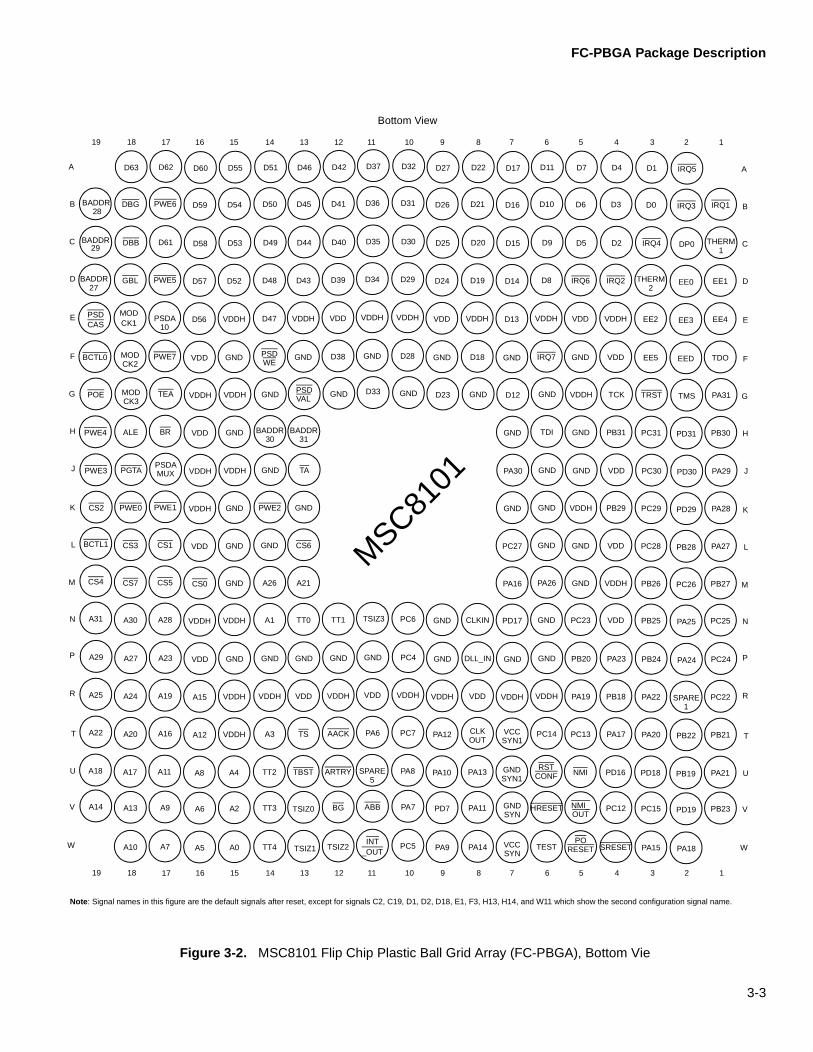
3-3
FC-PBGA Package Description
Figure 3-2. MSC8101 Flip Chip Plastic Ball Grid Array (FC-PBGA), Bottom Vie
134 256781014 13 12 11 9
B
C
D
E
F
G
H
N
M
L
J
K
P
A
Bottom View
T
U
1516
V
W
EE1
PA29
PA28
1819 17
THERM
IRQ1
PA31
PB30
TDO
EE4
PA27
PB27
PC25
PC24
PC22
PB21
PB23
PA21
IRQ5
EE0
PD30
PD29
DP0
IRQ3
TMS
PD31
EED
EE3
PB28
PC26
PA25
PA24
SPARE
PB22
PD19
PA18
PB19
D1
THERM
PC30
PC29
IRQ4
D0
TRST
PC31
EE5
EE2
PC28
PB26
PB25
PB24
PA22
PA20
PC15
PA15
PD18
D4
IRQ2
VDD
PB29
D2
D3
TCK
PB31
VDD
VDDH
VDD
VDDH
VDD
PA23
PB18
PA17
PC12
SRESET
PD16
D7
IRQ6
GND
VDDH
D5
D6
VDDH
GND
GND
VDD
GND
GND
PC23
PB20
PA19
PC13
NMI_
PO
NMI
D17
D14
PA30
GND
D15
D16
D12
GND
GND
D13
PC27
PA16
PD17
GND
VDDH
VCC
GND
VCC
GND
D11
D8
GND
GND
D9
D10
GND
TDI
IRQ7
VDDH
GND
PA26
GND
GND
VDDH
PC14
HRESET
TEST
RST
D22
D19
D20
D21
GND
D18
VDDH
CLKIN
DLL_IN
VDD
CLK
PA11
PA14
PA13
D62
PWE5
PSDA
PWE1
D61
PWE6
TEA
BR
PWE7
PSDA
CS1
CS5
A28
A23
A19
A16
A9
A7
A11
D27
D24
D25
D26
D23
GND
VDD
GND
GND
VDDH
PA12
PD7
PA9
PA10
D32
D29
D30
D31
GND
D28
VDDH
PC6
PC4
VDDH
PC7
PA7
PC5
PA8
D37
D34
D35
D36
D33
GND
VDDH
GND
VDD
PA6
ABB
INT
SPARE
D42
D39
D40
D41
GND
D38
VDD
TT1
GND
VDDH
AACK
BG
ARTRY
D46
D43
TA
GND
D44
D45
PSD
BADDR
GND
VDDH
CS6
A21
TT0
GND
VDD
TS
TBST
D51
D48
GND
PWE2
D49
D50
GND
BADDR
PSD
D47
GND
A26
A1
GND
VDDH
A3
TT3
TT4
TT2
D55
D52
VDDH
GND
D53
D54
VDDH
GND
GND
VDDH
GND
GND
VDDH
GND
VDDH
VDDH
A2
A0
A4
D60
D57
VDDH
VDDH
D58
D59
VDDH
VDD
VDD
D56
VDD
CS0
VDDH
VDD
A15
A12
A6
A5
A8
D63
GBL
PGTA
PWE0
DBB
DBG
MOD
ALE
MOD
CS3
CS7
A30
A27
A24
A20
A13
A10
A17
R
1
2
10
MODCK1
CK2
CK3
3130
MUX
CS2
1
SYN1OUT
5 CONFSYN1
OUTSYN
RESETSYN
VAL
BADDR
BADDR
BADDR
POE
PWE4
BCTL0
PSD
28
29
27
CAS
PWE3
BCTL1
CS4
A31
A29
A25
A22
A14
A18
WE
134 256781014 13 12 11 915161819 17
B
C
D
E
F
G
H
N
M
L
J
K
P
A
T
U
V
W
R
_OUT
MSC81
01
TSIZ1
TSIZ3
TSIZ0
TSIZ2
Note: Signal names in this figure are the default signals after reset, except for signals C2, C19, D1, D2, D18, E1, F3, H13, H14, and W11 which show the second configuration signal name.

3-4
FC-PBGA Package Description
Table 3-1. MSC8101 Signal Listing By Name
Signal Name Number
A0 W15
A1 N14
A2 V15
A3 T14
A4 U15
A5 W16
A6 V16
A7 W17
A8 U16
A9 V17
A10 W18
A11 U17
A12 T16
A13 V18
A14 V19
A15 R16
A16 T17
A17 U18
A18 U19
A19 R17
A20 T18
A21 M13
A22 T19
A23 P17
A24 R18
A25 R19
A26 M14
A27 P18
A28 N17
A29 P19
A30 N18
A31 N19
AACK T12

3-5
FC-PBGA Package Description
ABB V11
ALE H18
ARTRY U12
BADDR27 D19
BADDR28 B19
BADDR29 C19
BADDR30 H14
BADDR31 H13
BCTL0 F19
BCTL1 L19
BG V12
BNKSEL0 E18
BNKSEL1 F18
BNKSEL2 G18
BR H17
BRG1O H3
BRG1O V2
BRG2O J3
BRG2O N7
BRG3O K3
BRG4O L3
BRG5O L7
BRG6O M2
BRG7O N1
BRG8O P1
BTM0 E1
BTM1 F3
CD for FCC1 N10
CD for FCC2 P10
CD/RENA for SCC1 T6
CD/RENA for SCC2 V4
CLK1 H3
CLK2 J3
Table 3-1. MSC8101 Signal Listing By Name (Continued)
Signal Name Number

3-6
FC-PBGA Package Description
CLK3 K3
CLK4 L3
CLK5 L7
CLK6 M2
CLK7 N1
CLK8 P1
CLK9 N5
CLK10 R1
CLKIN N8
CLKOUT T8
COL for FCC1 G1
COL for FCC2 M1
CRS for FCC1 J7
CRS for FCC2 M3
CS0 M16
CS1 L17
CS2 K19
CS3 L18
CS4 M19
CS5 M17
CS6 L13
CS7 M18
CTS for FCC1 T10
CTS for FCC2 W10
CTS/CLSN for SCC1 K3
CTS/CLSN for SCC1 V3
CTS/CLSN for SCC2 L3
CTS/CLSN for SCC2 T5
D0 B3
D1 A3
D2 C4
D3 B4
D4 A4
Table 3-1. MSC8101 Signal Listing By Name (Continued)
Signal Name Number

3-7
FC-PBGA Package Description
D5 C5
D6 B5
D7 A5
D8 D6
D9 C6
D10 B6
D11 A6
D12 G7
D13 E7
D14 D7
D15 C7
D16 B7
D17 A7
D18 F8
D19 D8
D20 C8
D21 B8
D22 A8
D23 G9
D24 D9
D25 C9
D26 B9
D27 A9
D28 F10
D29 D10
D30 C10
D31 B10
D32 A10
D33 G11
D34 D11
D35 C11
D36 B11
D37 A11
Table 3-1. MSC8101 Signal Listing By Name (Continued)
Signal Name Number

3-8
FC-PBGA Package Description
D38 F12
D39 D12
D40 C12
D41 B12
D42 A12
D43 D13
D44 C13
D45 B13
D46 A13
D47 E14
D48 D14
D49 C14
D50 B14
D51 A14
D52 D15
D53 C15
D54 B15
D55 A15
D56 E16
D57 D16
D58 C16
D59 B16
D60 A16
D61 C17
D62 A17
D63 A18
DACK1 N5
DACK2 N1
DACK3 D5
DACK4 F6
DBB C18
DBG B18
DBREQ D2
Table 3-1. MSC8101 Signal Listing By Name (Continued)
Signal Name Number

3-9
FC-PBGA Package Description
DLLIN P8
DP0 C2
DP1 B1
DP2 D4
DP3 B2
DP4 C3
DP5 A2
DP6 D5
DP7 F6
DRACK1/DONE1 H2
DRACK2/DONE2 J2
DREQ1 R1
DREQ2 P1
DREQ3 C3
DREQ4 A2
EE0 D2
EE1 D1
EE2 E3
EE3 E2
EE4 E1
EE5 F3
EED F2
EXT_BG2 B1
EXT_BG3 C3
EXT_BR2 C2
EXT_BR3 B2
EXT_DBG2 D4
EXT_DBG3 A2
EXT1 H3
EXT2 N5
GBL D18
GND F11
GND F13
Table 3-1. MSC8101 Signal Listing By Name (Continued)
Signal Name Number

3-10
FC-PBGA Package Description
GND F15
GND F5
GND F7
GND F9
GND G10
GND G12
GND G14
GND G6
GND G8
GND H15
GND H5
GND H7
GND J14
GND J5
GND J6
GND K13
GND K15
GND K6
GND K7
GND L14
GND L15
GND L5
GND L6
GND M15
GND M5
GND N6
GND N9
GND P11
GND P12
GND P13
GND P14
GND P15
GND P6
Table 3-1. MSC8101 Signal Listing By Name (Continued)
Signal Name Number

3-11
FC-PBGA Package Description
GND P7
GND P9
GNDSYN V7
GNDSYN1 U7
H8BIT B16
HA0 D14
HA1 C14
HA2 B14
HA3 A14
HACK/HACK E16
HCS1/HCS1 D15
HCS2/HCS2 A16
HD0 A10
HD1 G11
HD2 D11
HD3 C11
HD4 B11
HD5 A11
HD6 F12
HD7 D12
HD8 C12
HD9 B12
HD10 A12
HD11 D13
HD12 C13
HD13 B13
HD14 A13
HD15 E14
HDDS C16
HDS/HDS B15
HDSP D16
HPE D1
HRD/HRD C15
Table 3-1. MSC8101 Signal Listing By Name (Continued)
Signal Name Number

3-12
FC-PBGA Package Description
HREQ/HREQ A15
HRESET V6
HRRQ/HRRQ E16
HRW C15
HTRQ/HTRQ A15
HWR/HWR B15
INT_OUT W11
IRQ1 B1
IRQ1 D18
IRQ2 C19
IRQ2 D4
IRQ2 V11
IRQ3 B2
IRQ3 C18
IRQ3 H14
IRQ4 C3
IRQ5 A2
IRQ5 H13
IRQ6 D5
IRQ7 F6
IRQ7 W11
L1RSYNC for SI1 TDMA1 T11
L1RSYNC for SI2 TDMB2 K4
L1RSYNC for SI2 TDMC2 P3
L1RSYNC for SI2 TDMD2 P5
L1RXD for SI1 TDMA1 Serial U10
L1RXD for SI2 TDMB2 H1
L1RXD for SI2 TDMC2 M3
L1RXD for SI2 TDMD2 T2
L1RXD0 for SI1 TDMA1 Nibble U10
L1RXD1 for SI1 TDMA1 Nibble T2
L1RXD2 for SI1 TDMA1 Nibble V1
L1RXD3 for SI1 TDMA1 Nibble P3
Table 3-1. MSC8101 Signal Listing By Name (Continued)
Signal Name Number

3-13
FC-PBGA Package Description
L1TSYNC/GRANT for SI1 TDMA1 V10
L1TSYNC/GRANT for SI2 TDMB2 L2
L1TSYNC/GRANT for SI2 TDMC2 N3
L1TSYNC/GRANT for SI2 TDMD2 T1
L1TXD for SI1 TDMA1 Serial W9
L1TXD for SI2 TDMB2 H4
L1TXD for SI2 TDMC2 M1
L1TXD for SI2 TDMD2 V1
L1TXD0 for SI1 TDMA1 Nibble W9
L1TXD1 for SI1 TDMA1 Nibble P5
L1TXD2 for SI1 TDMA1 Nibble T1
L1TXD3 for SI1 TDMA1 Nibble N3
LIST1 for SI1 R1
LIST1 for SI2 T10
LIST2 for SI1 T6
LIST2 for SI2 N10
LIST3 for SI1 V4
LIST3 for SI2 W10
LIST4 for SI1 T5
LIST4 for SI2 P10
MODCK1 E18
MODCK2 F18
MODCK3 G18
MSNUM0 N2
MSNUM1 P2
MSNUM2 U8
MSNUM3 T9
MSNUM4 V8
MSNUM5 U9
NMI U5
NMI_OUT V5
PA6 T11
PA7 V10
Table 3-1. MSC8101 Signal Listing By Name (Continued)
Signal Name Number

3-14
FC-PBGA Package Description
PA8 U10
PA9 W9
PA10 U9
PA11 V8
PA12 T9
PA13 U8
PA14 W8
PA15 W3
PA16 M7
PA17 T4
PA18 W2
PA19 R5
PA20 T3
PA21 U1
PA22 R3
PA23 P4
PA24 P2
PA25 N2
PA26 M6
PA27 L1
PA28 K1
PA29 J1
PA30 J7
PA31 G1
PB18 R4
PB19 U2
PB20 P5
PB21 T1
PB22 T2
PB23 V1
PB24 P3
PB25 N3
PB26 M3
Table 3-1. MSC8101 Signal Listing By Name (Continued)
Signal Name Number

3-15
FC-PBGA Package Description
PB27 M1
PB28 L2
PB29 K4
PB30 H1
PB31 H4
PBS0 K18
PBS1 K17
PBS2 K14
PBS3 J19
PBS4 H19
PBS5 D17
PBS6 B17
PBS7 F17
PC4 P10
PC5 W10
PC6 N10
PC7 T10
PC12 V4
PC13 T5
PC14 T6
PC15 V3
PC22 R1
PC23 N5
PC24 P1
PC25 N1
PC26 M2
PC27 L7
PC28 L3
PC29 K3
PC30 J3
PC31 H3
PD7 V9
PD16 U4
Table 3-1. MSC8101 Signal Listing By Name (Continued)
Signal Name Number

3-16
FC-PBGA Package Description
PD17 N7
PD18 U3
PD19 V2
PD29 K2
PD30 J2
PD31 H2
PGPL0 E17
PGPL1 F14
PGPL2 G19
PGPL3 E19
PGPL4 J18
PGPL5 J17
PGTA J18
POE G19
PORESET W5
PPBS J18
PSDA10 E17
PSDAMUX J17
PSDCAS E19
PSDDQM0 K18
PSDDQM1 K17
PSDDQM2 K14
PSDDQM3 J19
PSDDQM4 H19
PSDDQM5 D17
PSDDQM6 B17
PSDDQM7 F17
PSDRAS G19
PSDVAL G13
PSDWE F14
PUPMWAIT J18
PWE0 K18
PWE1 K17
Table 3-1. MSC8101 Signal Listing By Name (Continued)
Signal Name Number

3-17
FC-PBGA Package Description
PWE2 K14
PWE3 J19
PWE4 H19
PWE5 D17
PWE6 B17
PWE7 F17
Reserved A17
Reserved A18
Reserved C2
Reserved C17
Reserved C19
Reserved H14
Reserved H13
RSTCONF U6
RTS for FCC1 J7
RTS for FCC2 L2
RTS/TENA for SCC1 K2
RTS/TENA for SCC2 L2
RX_DV for FCC1 M1
RX_DV for FCC2 H1
RX_ER for FCC1 M3
RX_ER for FCC2 L2
RXADDR0 for FCC1 UTOPIA 8 T6
RXADDR1 for FCC1 UTOPIA 8 V4
RXADDR2 for FCC1 UTOPIA 8 N10
RXADDR2/RXCLAV1 for FCC1 UTOPIA 8 N10
RXADDR3 for FCC1 UTOPIA 8 K2
RXADDR4 for FCC1 UTOPIA 8 U3
RXCLAV for FCC1 UTOPIA 8 M3
RXCLAV0 for FCC1 UTOPIA 8 M3
RXCLAV2 for FCC1 UTOPIA 8 K2
RXCLAV3 for FCC1 UTOPIA 8 V4
RXD for FCC1 transparent/HDLC serial T4
Table 3-1. MSC8101 Signal Listing By Name (Continued)
Signal Name Number

3-18
FC-PBGA Package Description
RXD for FCC2 transparent/HDLC serial T1
RXD for SCC1 H2
RXD for SCC2 H4
RXD0 for FCC1 MII/HDLC nibble T4
RXD0 for FCC1 UTOPIA 8 U9
RXD0 for FCC2 MII/HDLC nibble T1
RXD1 for FCC1 MII/HDLC nibble M7
RXD1 for FCC1 UTOPIA 8 V8
RXD1 for FCC2 MII/HDLC nibble P5
RXD2 for FCC1 MII/HDLC nibble W3
RXD2 for FCC1 UTOPIA 8 T9
RXD2 for FCC2 MII/HDLC nibble U2
RXD3 for FCC1 MII/HDLC nibble W8
RXD3 for FCC1 UTOPIA 8 U8
RXD3 for FCC2 MII/HDLC nibble R4
RXD4 for FCC1 UTOPIA 8 W8
RXD5 for FCC1 UTOPIA 8 W3
RXD6 for FCC1 UTOPIA 8 M7
RXD7 for FCC1 UTOPIA 8 T4
RXENB for FCC1 K1
RXPRTY for FCC1 UTOPIA 8 N7
RXSOC for FCC1 M1
SCL R4
SDA U2
SMRXD for SMC1 P10
SMRXD for SMC2 U10
SMSYN for SMC1 V9
SMSYN for SMC2 V10
SMTXD for SMC1 W10
SMTXD for SMC2 W9
SMTXD for SMC2 V3
SPARE1 R2
SPARE5 U11
Table 3-1. MSC8101 Signal Listing By Name (Continued)
Signal Name Number

3-19
FC-PBGA Package Description
SPICLK U3
SPIMISO U4
SPIMOSI N7
SPISEL V2
SRESET W4
TA J13
TBST U13
TC0 E18
TC1 F18
TC2 G18
TCK G4
TDI H6
TDO F1
TEA G17
TEST W6
TGATE1 H3
TGATE2 L7
THERM1 C1
THERM2 D3
TIN1/TOUT2 L3
TIN2 K3
TIN3/TOUT4 P1
TIN4 N1
TMCLK M2
TMS G2
TOUT1 J3
TOUT3 M2
TRST G3
TS T13
TSIZ0 V13
TSIZ1 W13
TSIZ2 W12
TSIZ3 N11
Table 3-1. MSC8101 Signal Listing By Name (Continued)
Signal Name Number

3-20
FC-PBGA Package Description
TT0 N13
TT1 N12
TT2 U14
TT3 V14
TT4 W14
TX_EN for FCC1 MII K1
TX_EN for FCC2 MII K4
TX_ER for FCC1 MII J1
TX_ER for FCC2 MII H4
TXADDR0 for FCC1 UTOPIA 8 V3
TXADDR1 for FCC1 UTOPIA 8 T5
TXADDR2 for FCC1 UTOPIA 8 T10
TXADDR2 for FCC1 UTOPIA 8 T10
TXADDR3 for FCC1 UTOPIA 8 V9
TXADDR4 for FCC1 UTOPIA 8 V2
TXCLAV for FCC1 UTOPIA 8 J7
TXCLAV0 for FCC1 UTOPIA 8 J7
TXCLAV1 for FCC1 UTOPIA 8 T10
TXCLAV2 for FCC1 UTOPIA 8 V9
TXCLAV3 for FCC1 UTOPIA 8 V2
TXD for FCC1 transparent/HDLC serial W2
TXD for FCC2 transparent/HDLC serial T2
TXD for SCC1 J2
TXD for SCC2 H1
TXD0 for FCC1 MII/HDLC nibble W2
TXD0 for FCC1 UTOPIA 8 N2
TXD0 for FCC2 MII/HDLC nibble T2
TXD1 for FCC1 MII/HDLC nibble R5
TXD1 for FCC1 UTOPIA 8 P2
TXD1 for FCC2 MII/HDLC nibble V1
TXD2 for FCC1 MII/HDLC nibble T3
TXD2 for FCC1 UTOPIA 8 P4
TXD2 for FCC2 MII/HDLC nibble P3
Table 3-1. MSC8101 Signal Listing By Name (Continued)
Signal Name Number

3-21
FC-PBGA Package Description
TXD3 for FCC1 MII/HDLC nibble U1
TXD3 for FCC1 UTOPIA 8 R3
TXD3 for FCC2 MII/HDLC nibble N3
TXD4 for FCC1 UTOPIA 8 U1
TXD5 for FCC1 UTOPIA 8 T3
TXD6 for FCC1 UTOPIA 8 R5
TXD7 for FCC1 UTOPIA 8 W2
TXENB for FCC1 G1
TXPRTY for FCC1 UTOPIA 8 U4
TXSOC for FCC1 J1
VCCSYN W7
VCCSYN1 T7
VDD E12
VDD E5
VDD E9
VDD F16
VDD F4
VDD H16
VDD J4
VDD L16
VDD L4
VDD N4
VDD P16
VDD R11
VDD R13
VDD R8
VDDH E10
VDDH E11
VDDH E13
VDDH E15
VDDH E4
VDDH E6
VDDH E8
Table 3-1. MSC8101 Signal Listing By Name (Continued)
Signal Name Number

3-22
FC-PBGA Package Description
VDDH G15
VDDH G16
VDDH G5
VDDH J15
VDDH J16
VDDH K16
VDDH K5
VDDH M4
VDDH N15
VDDH N16
VDDH R10
VDDH R12
VDDH R14
VDDH R15
VDDH R6
VDDH R7
VDDH R9
VDDH T15
Table 3-2. MSC8101 Signal Listing by Pin Designator
Number Signal Name
A2 IRQ5 / DP5 / DREQ4 / EXT_DBG3
A3 D1
A4 D4
A5 D7
A6 D11
A7 D17
A8 D22
A9 D27
A10 D32 / HD0
A11 D37 / HD5
A12 D42 / HD10
A13 D46 / HD14
A14 D51 / HA3
Table 3-1. MSC8101 Signal Listing By Name (Continued)
Signal Name Number

3-23
FC-PBGA Package Description
A15 D55 / HREQ / HTRQ
A16 D60 / HCS2
A17 D62 / Reserved
A18 D63 / Reserved
B1 IRQ1 / DP1 / EXT_BG2
B2 IRQ3 / DP3 / EXT_BR3
B3 D0
B4 D3
B5 D6
B6 D10
B7 D16
B8 D21
B9 D26
B10 D31
B11 D36 / HD4
B12 D41 / HD9
B13 D45 / HD13
B14 D50 / HA2
B15 D54 / HDS / HWR
B16 D59 / H8BIT
B17 PWE6 / PSDDQM6 / PBS6
B18 DBG
B19 BADDR28
C1 THERM1
C2 Reserved / DP0 / EXT_BR2
C3 IRQ4 / DP4 / DREQ3 / EXT_BG3
C4 D2
C5 D5
C6 D9
C7 D15
C8 D20
C9 D25
C10 D30
C11 D35 / HD3
C12 D40 / HD8
C13 D44 / HD12
C14 D49 / HA1
C15 D53 / HRW / HRD
Table 3-2. MSC8101 Signal Listing by Pin Designator (Continued)
Number Signal Name

3-24
FC-PBGA Package Description
C16 D58 / HDDS
C17 D61
C18 DBB / IRQ3
C19 BADDR29 / IRQ2
D1 HPE / EE1
D2 DBREQ / EE0
D3 THERM2
D4 IRQ2 / DP2 / EXT_DBG2
D5 IRQ6 / DP6 / DACK3
D6 D8
D7 D14
D8 D19
D9 D24
D10 D29
D11 D34 / HD2
D12 D39 / HD7
D13 D43 / HD11
D14 D48 / HA0
D15 D52 / HCS1
D16 D57 / HDSP
D17 PWE5 / PSDDQM5 / PBS5
D18 IRQ1 / GBL
D19 BADDR27
E1 BTM0 / EE4
E2 EE3
E3 EE2
E4 VDDH
E5 VDD
E6 VDDH
E7 D13
E8 VDDH
E9 VDD
E10 VDDH
E11 VDDH
E12 VDD
E13 VDDH
E14 D47 / HD15
E15 VDDH
Table 3-2. MSC8101 Signal Listing by Pin Designator (Continued)
Number Signal Name

3-25
FC-PBGA Package Description
E16 D56 / HACK / HRRQ
E17 PSDA10 / PGPL0
E18 MODCK1 / TC0 / BNKSEL0
E19 PSDCAS / PGPL3
F1 TDO
F2 EED
F3 BTM1 / EE5
F4 VDD
F5 GND
F6 IRQ7 / DP7 / DACK4
F7 GND
F8 D18
F9 GND
F10 D28
F11 GND
F12 D38 / HD6
F13 GND
F14 PSDWE / PGPL1
F15 GND
F16 VDD
F17 PWE7 / PSDDQM7 / PBS7
F18 MODCK2 / TC1 / BNKSEL1
F19 BCTL0
G1 PA31 / FCC1:UTOPIA8:TXENB / FCC1:MII:COL
G2 TMS
G3 TRST
G4 TCK
G5 VDDH
G6 GND
G7 D12
G8 GND
G9 D23
G10 GND
G11 D33 / HD1
G12 GND
G13 PSDVAL
G14 GND
G15 VDDH
Table 3-2. MSC8101 Signal Listing by Pin Designator (Continued)
Number Signal Name

3-26
FC-PBGA Package Description
G16 VDDH
G17 TEA
G18 MODCK3 / TC2 / BNKSEL2
G19 POE / PSDRAS / PGPL2
H1 PB30 / FCC2:MII:RX_DV / SCC2:TXD / TDBM2:L1RXD
H2 PD31 / SCC1:RXD / DRACK1 / DONE1
H3 PC31 / BRG1O / CLK1 / TGATE1
H4 PB31 / FCC2:MII:TX_ER / SCC2:RXD / TDMB2:L1TXD
H5 GND
H6 TDI
H7 GND
H13 Reserved / BADDR31 / IRQ5
H14 Reserved / BADDR30 / IRQ3
H15 GND
H16 VDD
H17 BR
H18 ALE
H19 PWE4 / PSDDQM4 / PBS4
J1 PA29 / FCC1:UTOPIA8:TXSOC / FCC1:MII:TX_ER
J2 PD30 / SCC1:TXD / DMA:DRACK2/DONE2
J3 PC30 / EXT1 / BRG2O / CLK2 / TOUT1
J4 VDD
J5 GND
J6 GND
J7 PA30 / FCC1:UTOPIA8:TXCLAV / FCC1:UTOPIA8:TXCLAV0 / FCC1:MII:CRS / FCC1:HDLC and transparent:RTS
J13 TA
J14 GND
J15 VDDH
J16 VDDH
J17 PSDAMUX / PGPL5
J18 PGTA / PUPMWAIT / PPBS / PGPL4
J19 PWE3 / PSDDQM3 / PBS3
K1 PA28 / FCC1:UTOPIA8:RXENB / FCC1:MII:TX_EN
K2 PD29 / FCC1:UTOPIA8:RXADDR3 / FCC1:UTOPIA8:RXCLAV2 / SCC1:RTS/TENA
K3 PC29 / SCC1:CTS / SCC1:CLSN / BRG3O / CLK3 / TIN2
K4 PB29 / FCC2:MII:TX_EN / TDMB2:L1RSYNC
Table 3-2. MSC8101 Signal Listing by Pin Designator (Continued)
Number Signal Name

3-27
FC-PBGA Package Description
K5 VDDH
K6 GND
K7 GND
K13 GND
K14 PWE2 / PSDDQM2 / PBS2
K15 GND
K16 VDDH
K17 PWE1 / PSDDQM1 / PBS1
K18 PWE0 / PSDDQM0 / PBS0
K19 CS2
L1 PA27 / FCC1:UTOPIA8:RXSOC / FCC1:MII:RX_DV
L2 PB28 / FCC2:RX_ER / FCC2:HDLC:RTS / SCC2:RTS/TENA / TDMB2:L1TSYNC
L3 PC28 / SCC2:CTS/CLSN / BRG4O / CLK4 / TIN1/TOUT2
L4 VDD
L5 GND
L6 GND
L7 PC27 / CLK5 / BRG5O / TGATE2
L13 CS6
L14 GND
L15 GND
L16 VDD
L17 CS1
L18 CS3
L19 BCTL1
M1 PB27 / FCC2:MII:COL / TDMC2:L1TXD
M2 PC26 / TMCLK / BRG6O / CLK6 / TOUT3
M3 PB26 / FCC2:MII:CRS / TDMC2:L1RXD
M4 VDDH
M5 GND
M6 PA26 / FCC1:UTOPIA8:RXCLAV / FCC1:UTOPIA8:RXCLAV0 / FCC1:MII:RX_ER
M7 PA16 / FCC1:UTOPIA8:RXD6 / FCC1:MII and HDLC nibble:RXD1
M13 A21
M14 A26
M15 GND
M16 CS0
M17 CS5
M18 CS7
Table 3-2. MSC8101 Signal Listing by Pin Designator (Continued)
Number Signal Name

3-28
FC-PBGA Package Description
M19 CS4
N1 PC25 / DMA:DACK2 / BRG7O / CLK7 / TIN4
N2 PA25 / FCC1:UTOPIA8:TXD0 / SDMA:MSNUM0
N3 PB25 / FCC2:MII and HDLC nibble:TXD3 / TDMA1:nibble:L1TXD3 / TDMC2:L1TSYNC/GRANT
N4 VDD
N5 PC23 / EXT2 / DMA:DACK1 / CLK9
N6 GND
N7 PD17 / FCC1:UTOPIA8:RXPRTY / SPI:SPIMOSI / BRG2O
N8 CLKIN
N9 GND
N10 PC6 / FCC1:UTOPIA8:RXADDR2 / FCC1:UTOPIA8:RXADDR2/RXCLAV1 / FCC1:CD / SI2:LIST2
N11 TSIZ3
N12 TT1
N13 TT0
N14 A1
N15 VDDH
N16 VDDH
N17 A28
N18 A30
N19 A31
P1 PC24 / DMA:DREQ2 / BRG8O / CLK8 / TIN3/TOUT4
P2 PA24 / FCC1:UTOPIA8:TXD1 / SDMA:MSNUM1
P3 PB24 / FCC2:MII and HDLC nibble:TXD3 / TDMA1:nibble:L1RXD3 / TDMC2:L1RSYNC
P4 PA23 / FCC1:UTOPIA8:TXD2
P5 PB20 / FCC2:MII and HDLC nibble:RXD1 / TDMA1:nibble:L1TXD1 / TDMD2:L1RSYNC
P6 GND
P7 GND
P8 DLLIN
P9 GND
P10 PC4 / FCC2:CD / SMC1:SMRXD / SI2:LIST4
P11 GND
P12 GND
P13 GND
P14 GND
P15 GND
Table 3-2. MSC8101 Signal Listing by Pin Designator (Continued)
Number Signal Name

3-29
FC-PBGA Package Description
P16 VDD
P17 A23
P18 A27
P19 A29
R1 PC22 / SI1:LIST1 / DREQ1 / CLK10
R2 SPARE1
R3 PA22 / FCC1:UTOPIA8:TXD3
R4 PB18 / FCC2:MII and HDLC nibble:RXD3 / I2C:SCL
R5 PA19 / FCC1:UTOPIA8:TXD6 / FCC1:MII and HDLC nibble:TXD1
R6 VDDH
R7 VDDH
R8 VDD
R9 VDDH
R10 VDDH
R11 VDD
R12 VDDH
R13 VDD
R14 VDDH
R15 VDDH
R16 A15
R17 A19
R18 A24
R19 A25
T1 PB21 / FCC2:MII and HDLC nibble:RXD0 / FCC2:transparent and HDLC serial:RXD /TDMA1:nibble:L1TXD2 /
TDMD2:L1TSYNC/GRANT
T2 PB22 / FCC2:MII and HDLC nibble TXD0 / FCC2:transparent and HDLC serial TXD /TDMA1:nibble L1RXD1 /
TDMD2:L1RXD
T3 PA20 / FCC1:UTOPIA8 TXD5 / FCC1:MII and HDLC nibble TXD2
T4 PA17 / FCC1:UTOPIA8 RXD7 / FCC1:MII and HDLC nibble RXD0 / FCC1:transparent and HDLC serial RXD
T5 PC13 / FCC1:UTOPIA8:TXADDR1 / SCC2:CTS/CLSN / SI1:LIST4
T6 PC14 / FCC1:UTOPIA8:RXADDR0 / SCC1:CD/RENA / SI1:LIST2
T7 VCCSYN1
T8 CLKOUT
T9 PA12 / FCC1:UTOPIA8:RXD2 / SDMA:MSNUM3
T10 PC7 / FCC1:UTOPIA8:TXADDR2 / FCC1:UTOPIA8:TXADDR2/TXCLAV1 / FCC1:CTS / SI1:LIST1
T11 PA6 / TDMA1:L2RSYNC
Table 3-2. MSC8101 Signal Listing by Pin Designator (Continued)
Number Signal Name

3-30
FC-PBGA Package Description
T12 AACK
T13 TS
T14 A3
T15 VDDH
T16 A12
T17 A16
T18 A20
T19 A22
U1 PA21 / FCC1:TXD4 / FCC1:MII and HDLC nibble TXD3
U2 PB19 / FCC2:MII and HDLC nibble RXD2 / I2C:SDA
U3 PD18 / FCC1:UTOPIA8:RXADDR4 / FCC1:UTOPIA8:RXCLAV3 / SPI:SPICLK
U4 PD16 / FCC1:UTOPIA8:TXPRTY / SPI:SPIMISO
U5 NMI
U6 RSTCONF
U7 GNDSYN1
U8 PA13 / FCC1:UTOPIA8:RXD3 / SDMA:MSNUM2
U9 PA10 / FCC1:UTOPIA8:RXD0 / SDMA:MSNUM5
U10 PA8 / SMC2:SMRXD / TDMA1:serial L1RXD / TDMA1:nibble L1RXD0
U11 SPARE5
U12 ARTRY
U13 TBST
U14 TT2
U15 A4
U16 A8
U17 A11
U18 A17
U19 A18
V1 PB23 / FCC2:MII and HDLC nibble:TXD1 / TDMA1:nibble:L1RXD2 / TDMD2:L1TXD
V2 PD19 / FCC1:UTOPIA8:TXADDR4 / FCC1:UTOPIA:TXCLAV3 / SPI:SPISEL / BRG1O
V3 PC15 / FCC1:UTOPIA8:TXADDR0 / SCC1:CTS/CLSN / SMC2:SMTXD
V4 PC12 / FCC1:UTOPIA8:RXADDR1 / SCC2:CD/RENA / SI1:LIST3
V5 NMI_OUT
V6 HRESET
V7 GNDSYN
V8 PA11 / FCC1:UTOPIA8:RXD1 / SDMA:MSNUM4
V9 PD7 / FCC1:UTOPIA8:TXADDR3 / FCC1:UTOPIA8:TXCLAV2 / SMC1:SMSYN
Table 3-2. MSC8101 Signal Listing by Pin Designator (Continued)
Number Signal Name

3-31
FC-PBGA Package Description
V10 PA7 / SMC2:SMSYN / TDMA1:L1TSYNC/GRANT
V11 ABB / IRQ2
V12 BG
V13 TSIZ0
V14 TT3
V15 A2
V16 A6
V17 A9
V18 A13
V19 A14
W2 PA18 / FCC1:UTOPIA8:TXD7 / FCC1:MII and HDLC nibble:TXD0 /FCC1:transparent and HDLC serial:TXD
W3 PA15 / FCC1:UTOPIA8:RXD5 / FCC1:MII and HDLC nibble:RXD2
W4 SRESET
W5 PORESET
W6 TEST
W7 VCCSYN
W8 PA14 / FCC1:UTOPIA8 RXD4 / FCC1:MII and HDLC nibble:RXD3
W9 PA9 / SMC2:SMTXD / TDMA1:serial:L1TXD /TDMA1:nibble:L1TXD0
W10 PC5 / FCC2:CTS / SMC1:SMTXD / SI2:LIST3
W11 IRQ7 / INT_OUT
W12 TSIZ2
W13 TSIZ1
W14 TT4
W15 A0
W16 A5
W17 A7
W18 A10
Table 3-2. MSC8101 Signal Listing by Pin Designator (Continued)
Number Signal Name

3-32
FC-PBGA Package Mechanical Drawing
3.3 FC-PBGA Package Mechanical Drawing
Figure 3-3. MSC8101 Mechanical Information, 332-pin FC-PBGA Package
DIM MIN MAXMillimeters
AA1A2A3b 0.40 0.60D
D1D2 10.35 10.55eEE1 14.40 REFE2 9.30 9.50
Notes:1. Dimensions and tolerancing per
ASME Y14.5, 1994.
2. Dimensions in millimeters.
3. Dimension b is the maximum solder ball diameter measured parallel to Datum A.
4. Primary Datum A and the seating plane are defined by the spherical crowns of the solder balls.
CASE 1169-01
17.00 BSC0.80 BSC
14.40 REF17.00 BSC
0.80 0.920.90 1.100.30 0.50— 2.60

4-1
Chapter 4
Design Considerations
4.1 Thermal Design ConsiderationsThe average chip-junction temperature, TJ, in °C can be obtained from the following:
Equation 1: TJ = TA + (PD • θJA)
where
TA = ambient temperature °C
θJA = package thermal resistance, junction to ambient, °C/W
PD = PINT + PI/O in W
PINT = IDD × VDD in W—chip internal power
PI/O = power dissipation on output pins in W—user determined
The user should set TA and PD such that TJ does not exceed the maximum operating conditions. In case TJ is too high, the user should either lower the ambient temperature or the power dissipation of the chip.

4-2
Electrical Design Considerations
4.2 Electrical Design ConsiderationsThe input voltage must not exceed the I/O supply VDDH by more than 2.5 V at any time, including during power-on reset. In turn, VDDH can exceed VDD/VCCSYN by more than 3.3 V during power-on reset, but for no more than 100 ms. VDDH should not exceed VDD/VCCSYN by more than 2.1 V during normal operation. VDD/VCCSYN must not exceed VDDH by more than 0.4 V at any time, including during power-on reset. Therefore the recommendation is to use "bootstrap" diodes between the power rails, as shown in Figure 4-1..
Select the bootstrap diodes such that a nominal VDD/VCCSYN is sourced from the VDDH power supply until the VDD/VCCSYN power supply becomes active. In Figure 4-1., four MUR420 Schottky barrier diodes are connected in series; each has a forward voltage (VF) of 0.6 V at high currents, so these diodes provide a 2.4 V drop, maintaining 0.9 V on the 1.6 V power line. Once the core/PLL power supply stabilizes at 1.6 V, the bootstrap diodes will be reverse biased with negligible leakage current. The VF should be effective at the current levels required by the processor. Do not use diodes with a nominal VF that drops too low at high current.
4.3 Power ConsiderationsThe internal power dissipation consists of three components:
PINT = PCORE + PSIU + PCPM
The power dissipation depends on the operating frequency of the different portions of the chip. The numbers given in Table 4-1 refer to 300 MHz core frequency, 150 MHz CPM frequency, and 100 MHz SIU frequency.
To determine the power dissipation at a given frequency, the following equations should be applied:
PCORE (f) = ((PCORE – PLCO)/300) × f + PLCO
PSIU (f) = ((PSIU – PLSI)/100) × f + PLSI
PCPM (f) = ((PCPM – PLCP)/150) × f + PLCP
Where f is the operating frequency in MHz and all power numbers are in mW.
To determine a total power dissipation in a specific application, the following equation should be applied for each I/O output pin:
Equation 2: P = C × VDDH2 × f × 10–3
Where: P = power in mW, C = load capacitance in pF, f = output switching frequency in MHz.
Figure 4-1. Bootstrap Diodes for Power-Up Sequencing
I/O Power
Core/PLLSupply
MUR420
MUR420
MUR420
MUR420
3.3 V (VDDH)
1.6 V (VDD/VCCSYN)

4-3
Power Considerations
For an application in which external data memory is used in a 32-bit single bus mode and no other outputs are active, the core runs at 200 MHz, the CPM runs at 100 MHz and the SIU runs at 50 MHz, power dissipation is calculated as follows:
Assumptions:
• External data memory is accessed every second cycle with 10% of address pins switching.• External data memory writes occurs once every eight cycles with 50% of data pins switching.• Each address and data pin has a 30 pF total load at the pin.• The application operates at VDDH = 3.3 V.
Since the address pins switch once at every second cycle, the address pins frequency is a quarter of the bus frequency (that is, 25 MHz).
For the same reason the data pins frequency is 3.125 MHz.
Calculating internal power:
PCORE (200) = ((PCORE – PLCO)/300) × 200 + PLCO =((250 – 3) / 300 × 200 + 3=168
PSIU (50) = ((PSIU – PLSI) / 100) × 50 + PLSI = ((70 – 2) / 100) × 50 + 2 = 36PCPM (100) = ((PCPM – PLCP) / 150) × 100 + PLCP = ((210 – 6) / 150) × 100 + 6 = 142PINT = PCORE(200) + PSIU(50) + PCPM(100) =168 + 36 + 142 = 346
PD = PINT + PI/O = 346 + 67 = 413
Maximum allowed ambient temperature is:
TA = TJ – (PD × θJA)
Table 4-1. Power Dissipation
Pins# of pins switching
× C × VDDH2 × f × 10–3 Power in mW
AddressData, HRD, HRW
CLKOUT
4 341
× 30× 30× 30
× 3.32
× 3.32
× 3.32
× 12.5 × 10–3
× 3. 125 × 10–3
× 50 × 10–3
16.2534.75
16
Total PI/O 67

4-4
Layout Practices
4.4 Layout PracticesEach VCC and VDD pin on the MSC8101 should be provided with a low-impedance path to the board’s power supply. Similarly, each GND pin should be provided with a low-impedance path to ground. The power supply pins drive distinct groups of logic on the chip. The VCC power supply should be bypassed to ground using at least four 0.1 µF by-pass capacitors located as closely as possible to the four sides of the package. The capacitor leads and associated printed circuit traces connecting to chip VCC, VDD, and GND should be kept to less than half an inch per capacitor lead. A four-layer board is recommended, employing two inner layers as VCC and GND planes.
All output pins on the MSC8101 have fast rise and fall times. Printed circuit board (PCB) trace interconnection length should be minimized in order to minimize undershoot and reflections caused by these fast output switching times. This recommendation particularly applies to the address and data busses. Maximum PCB trace lengths of six inches are recommended. Capacitance calculations should consider all device loads as well as parasitic capacitances due to the PCB traces. Attention to proper PCB layout and bypassing becomes especially critical in systems with higher capacitive loads because these loads create higher transient currents in the VCC, VDD, and GND circuits. Pull up all unused inputs or signals that will be inputs during reset. Special care should be taken to minimize the noise levels on the PLL supply pins.
There are 2 pairs of PLL supply pins: VCCSYN-GNDSYN and VCCSYN1-GNDSYN1. Each pair supplies one PLL. To ensure internal clock stability, filter the power to the VCCSYN and VCCSYN1 inputs with a circuit similar to the one in Figure 4-2.. To filter as much noise as possible, place the circuit as close as possible to VCCSYN and VCCSYN1. The 0.01-µF capacitor should be closest to VCCSYN and VCCSYN1, followed by the 10-µF capacitor, the 10-nH inductor, and finally the 10-Ω resistor to VDD. These traces should be kept short and direct.
GNDSYN and GNDSYN1 should be provided with an extremely low impedance path to ground and should be bypassed to VCCSYN and VCCSYN1, respectively, by a 0.01-µF capacitor located as close as possible to the chip package. The user should also bypass GNDSYN and GNDSYN1 to VCCSYN and VCCSYN1 with a 0.01-µF capacitor as closely as possible to the chip package
Figure 4-2. VCCSYN and VCCSYN1 Bypass
VDD
0.01 µF10 µF
VCCSYN
10Ω 10nH

Index
Index-1
A
AC timings 2-7Address Acknowledge signal 1-10Address Bus Busy signal 1-9Address Bus signal 1-8Address Latch Enable (ALE) 1-16Address Retry signal 1-10applications iv
B
block diagram iBoot Mode 0–1 (BTM[0–1]) signals 1-7Buffer Control 0 (BCTL0) 1-16Buffer Control 1 (BCTL1) 1-16Burst Address 27–28 (BADDR[27–28]) 1-16Burst Address 29 signal 1-9Burst Address 30 signal 1-9BUS DF 2-4Bus Grant signal 1-9Bus Output Enable signal 1-17Bus Parity Byte Select signal 1-17Bus Request signal 1-9Bus SDRAM A10 signal 1-16Bus SDRAM Address Multiplexer signal 1-17Bus SDRAM CAS signal 1-17Bus SDRAM RAS signal 1-17Bus SDRAM Write Enable signal 1-16Bus Transfer Start signal 1-10Bus UPM General-Purpose Line 0 signal 1-16Bus UPM General-Purpose Line 1 signal 1-16Bus UPM General-Purpose Line 2 signal 1-17Bus UPM General-Purpose Line 3 signal 1-17Bus UPM General-Purpose Line 4 signal 1-17Bus UPM General-Purpose Line 5 signal 1-17Bus UPM Wait signal 1-17Bus Write Enable (PWE[0–7]) 1-16
C
capabilities ivChip Select (CS0–7) 1-16clock 1-5
JTAG 2-23operation 2-8
clocksSystem Clock Control Register (SCCR) 2-5System Clock Mode Register (SCMR) 2-5
Communications Processor Module (CPM) iii
coprocessor iiiCPM inputs 2-20
D
Data Bus 1-11Data Bus Bit 32–47 signals 1-10Data Bus Bit 48–51 signals 1-10Data Bus Bit 52 signal 1-11Data Bus Bit 53 signal 1-11Data Bus Bit 54 signal 1-11Data Bus Bit 55 signal 1-11Data Bus Bit 56 signal 1-12Data Bus Bit 57 signal 1-12Data Bus Bit 58 signal 1-12Data Bus Bit 59 signal 1-12Data Bus Bit 60 signal 1-12Data Bus Bit 61–63 signals 1-12Data Bus Busy signal 1-10Data Bus Grant signal 1-10Data Bus Most Significant Word (D[0–31]) 1-10Data Parity 0 (DP0) 1-13Data Parity 1 (DP1) 1-13Data Parity 2 (DP2) 1-13Data Parity 3 (DP3) 1-13Data Parity 4 (DP4) 1-14Data Parity 5 (DP5) 1-14Data Parity 6 (DP6) 1-14Data Parity 7 (DP7) 1-14Data Valid (PSDVAL) 1-15DC electrical characteristics 2-3Debug Request (DBREQ) signal 1-6design considerations
electrical 4-2layout practices 4-4power 4-2power dissipation 4-3thermal 4-1
DMA Acknowledge 3 (DACK3) 1-14DMA Acknowledge 4(DACK4) 1-14DMA controller iiiDMA Request 3 (DREQ3) 1-14DMA Request 4 (DREQ4) 1-14documentation iv
E
EE signals 2-22electrical characteristics
DC 2-3

Index
Index-2
enhanced filter coprocessor iiiEOnCE Event 0(EE0) signal 1-6EOnCE Event 1(EE1) signal 1-6EOnCE Event 2EE2) signal 1-6EOnCE Event 3 (EE3) signal 1-6EOnCE Event 4 (EE4) signal 1-7EONCE Event 5 (EE5) signal 1-7EOnCE Event Detection (EED) signal 1-7External Bus Grant 2 (EXT_BG2) 1-13External Bus Grant 3 (EXT_BG3) 1-14External Bus Request 3 (EXT_BR3) 1-13External Data Bus Grant 2 (EXT_DBG2) 1-13External Data Bus Grant 3 (EXT_DBG3) 1-14External PPC Bus Request 2 (EXT_BR2) 1-13
F
FCC internal clock diagram 2-20FC-PBGA
mechanical drawing 3-32features
150 MHz Communications Processor Module (CPM) iii
DMA controller iiienhanced 16-bit parallel Host Interface
(HID16) iiiEnhanced Filter Coprocessor iiion-chip SRAM iiiPLLs iiiPowerPC bus interface iiiprocess technology iiiprogrammable memory controller iiiSC140 core iiismall foot print package iiivery low power consumption iii
filter coprocessor iiifrequencies
maximum 2-4functional signal groups 1-1
G
Global signal 1-8GPCM TA signal 1-17
H
H8BIT (H8BIT) 1-12HDI08 timing 2-15HID16 iiiHost Acknowledge (HACK) 1-12
Host Address Line 0 signal 1-10Host Chip Select signal 1-11Host Data signal 1-10Host Data Strobe (HDS) 1-11Host Data Strobe Polarity (HDSP) 1-12Host Dual Data Strobe (HDDS) 1-12host interface iiiHost Interface timing 2-15Host Port Enable(HPE) signal 1-6Host Read Strobe signal 1-11Host Read Write Select signal 1-11Host Request (HREQ) 1-11Host Write Data Strobe (HWR) 1-11HRESET 1-7
I
input voltage 2-1inputs
CPM 2-20SIU 2-13
Interrupt Output (INT_OUT) 1-15Interrupt Request 1 (IRQ1) 1-13Interrupt Request 2 (IRQ2) 1-9, 1-13Interrupt Request 3 (IRQ3) 1-9, 1-10, 1-13Interrupt Request 4 (IRQ4) 1-14Interrupt Request 5 (IRQ5) 1-9, 1-14Interrupt Request 6 (IRQ6) 1-14Interrupt Request 7 (IRQ7) 1-14, 1-15
J
JTAG Portreset timing diagram 2-24timing 2-22
JTAG signals 2-22junction temperature 2-1
L
layout practices 4-4
M
maximum frequencies 2-4maximum ratings 2-1maximum ratings, 2-1MSC8101
block diagram idescription i

Index
Index-3
N
networking capabilities ivNon-Maskable Interrupt (NMI) 1-15Non-Maskable Interrupt Output(NMI_OUT) 1-15non-multiplexed bus timings
read 2-17write 2-18
O
outputsSIU 2-13
P
package iiiFC-PBGA description 3-32
pinoutbottom view 3-3top view 3-2
PIO, timer, and DMA signal diagram 2-21PLLs iiiPORESET 1-7power 1-4power considerations 4-2power consumption iiipower dissipation 4-3power-on reset flow 2-9PowerPC bus interface iiiprocess technology iiiproduct documentation ivprogrammable memory controller iii
R
Receive Host Request (HRRQ) 1-12reset
actions 2-9determine the PLL locking mode 2-9external configuration signals
Boot Mode 2-9EONCE Event Bit 0 2-9Host Port Enable 2-9Reset Configuration 2-9
hard reset 2-9hardware reset configuration 2-9host reset configuration 2-9PORESET 2-10power-on reset flow 2-9
program reset configuration word via the Host port 2-10
reset causes 2-8reset sources 2-8RSTCONF 2-11soft reset 2-9
RSTCONF 1-7
S
SC140 core iiiSCC/SMC/SPI/I2C external clock diagram 2-21SCC/SMC/SPI/I2C internal clock diagram 2-21SDRAM DQM (PSDDQM[0–7]) 1-16signal groupings 1-1signals 1-1
EE 2-22external 1-2JTAG 2-22memory controller
tick spacing 2-12multiplexed 1-1
signals, externalAddress Acknowledge (AACK) 1-10Address Bus (A[0–31]) 1-8Address Bus Busy (ABB) 1-9Address Retry (ARTRY) 1-10Burst Address 29 (BADDR29) 1-9Burst Address 30 (BADDR30) 1-9Bus Grant 1-9Bus Grant (BG) 1-9Bus Output Enable (POE) 1-17Bus Parity Byte Select (PPBS) 1-17Bus request signal (BR) 1-9Bus SDRAM A10 (PSDA10) 1-16Bus SDRAM Address Multiplexer
(PSDAMUX) 1-17Bus SDRAM CAS (PSDCAS) 1-17Bus SDRAM RAS (PSDRAS) 1-17Bus SDRAM Write Enable (PSDWE) 1-16Bus Transfer Start (TS) 1-10Bus UPM General Purpose Line 1
(PGPL1) 1-16Bus UPM General-Purpose Line 0
(PGPL0) 1-16Bus UPM General-Purpose Line 2
(PGPL2) 1-17Bus UPM General-Purpose Line 3
(PGPL3) 1-17Bus UPM General-Purpose Line 4 1-17

Index
Index-4
Bus UPM General-Purpose Line 4 (PGPL4) 1-17
Bus UPM General-Purpose Line 5 (PGPL5) 1-17
Data Bus Bit 48–51 (D[48–51]) 1-10Data Bus Bit 52 (D52) 1-11Data Bus Bit 53 (D53) 1-11Data Bus Bit 54 (D54) 1-11Data Bus Bit 55 (D55) 1-11Data Bus Bit 56 (D56) 1-12Data Bus Bit 57 (D57) 1-12Data Bus Bit 58 (D58) 1-12Data Bus Bit 59 (D59) 1-12Data Bus Bit 60 (D60) 1-12Data Bus Bit 61–63 (D[61–63]) 1-12Data Bus Bits 32–47 (D[32–47] ) 1-10Data Bus Busy (DBB) 1-10Data Bus Grant (DBG) 1-10Global (GBL) 1-8GPCM TA (PGTA) 1-17Host Address Line 0 (HA0) 1-10Host Chip Select (HCS) 1-11Host Data (H[0–15]) 1-10Host Read Strobe (HRD) 1-11Host Read Write Select 1-11Interrupt Request 1 (IRQ1) 1-13Interrupt Request 2 (IRQ2) 1-9, 1-13Interrupt Request 3 (IRQ3) 1-9, 1-10, 1-13Interrupt Request 4 (IRQ4) 1-14Interrupt Request 5 (IRQ5) 1-9, 1-14Interrupt Request 6 (IRQ6) 1-14Interrupt Request 7 (IRQ7) 1-14, 1-15Spare Pins (SPARE1, 5) 1-46
signals, external Bus UPM Wait (PUPMWAIT) 1-17
SIU inputs 2-13SIU outputs 2-13Spare Pins signal 1-46SPLL MF 2-4SPLL multiplication factor 2-4SPLL PDF 2-4SRAM iiiSRESET 1-7storage temperature 2-1supply voltage 2-1System Clock Control Register (SCCR) 2-5System Clock Mode Register (SCMR) 2-6
T
TAP timing diagram 2-23target applications ivTDM signal diagram 2-21Test Clock (TCK) input timing diagram 2-23thermal
design considerations 4-1thermal characteristics 2-2timing
interrupt 2-9mode select 2-9Reset 2-9Stop 2-9
timingsAC 2-7EE pins 2-22
Transfer Acknowledge (TA) 1-14Transfer Error Acknowledge (TEA) 1-15Transmit Host Request (HTRQ) 1-11
U
UPM Byte Select (PBS) 1-16

MSC8101/D
HOW TO REACH US:
USA/EUROPE/LOCATIONS NOT LISTED:
Motorola Literature Distribution; P.O. Box 5405, Denver, Colorado 80217 1-303-675-2140 or 1-800-441-2447
JAPAN:
Motorola Japan Ltd.; SPS, Technical Information Center, 3-20-1, Minami-Azabu Minato-ku, Tokyo 106-8573 Japan81-3-3440-3569
ASIA/PACIFIC:
Motorola Semiconductors H.K. Ltd.; Silicon Harbour Centre, 2 Dai King Street, Tai Po Industrial Estate, Tai Po, N.T., Hong Kong852-26668334
TECHNICAL INFORMATION CENTER:
1-800-521-6274
HOME PAGE:
http://www.motorola.com/semiconductors
Information in this document is provided solely to enable system and software implementers to use
Motorola products. There are no express or implied copyright licenses granted hereunder to design
or fabricate any integrated circuits or integrated circuits based on the information in this document.
Motorola reserves the right to make changes without further notice to any products herein. Motorola
makes no warranty, representation or guarantee regarding the suitability of its products for any
particular purpose, nor does Motorola assume any liability arising out of the application or use of any
product or circuit, and specifically disclaims any and all liability, including without limitation
consequential or incidental damages. “Typical” parameters which may be provided in Motorola data
sheets and/or specifications can and do vary in different applications and actual performance may
vary over time. All operating parameters, including “Typicals” must be validated for each customer
application by customer’s technical experts. Motorola does not convey any license under its patent
rights nor the rights of others. Motorola products are not designed, intended, or authorized for use as
components in systems intended for surgical implant into the body, or other applications intended to
support or sustain life, or for any other application in which the failure of the Motorola product could
create a situation where personal injury or death may occur. Should Buyer purchase or use Motorola
products for any such unintended or unauthorized application, Buyer shall indemnify and hold
Motorola and its officers, employees, subsidiaries, affiliates, and distributors harmless against all
claims, costs, damages, and expenses, and reasonable attorney fees arising out of, directly or
indirectly, any claim of personal injury or death associated with such unintended or unauthorized use,
even if such claim alleges that Motorola was negligent regarding the design or manufacture of the part.
Motorola and the Stylized M Logo are registered in the U.S. Patent and Trademark Office. OnCE and digital dna are trademarks of Motorola, Inc. All other product or service names are the property of their respective owners. Motorola, Inc. is an Equal Opportunity/Affirmative Action Employer.
© Motorola, Inc. 2001, 2002
Ordering InformationConsult a Motorola Semiconductor sales office or authorized distributor to determine product availability and place an order.
PartSupply Voltage
Package TypePin
Count
Core Frequency
(MHz)Order Number
MSC8101 1.6 V core3.3 V I/O
Flip Chip Plastic Ball Grid Array (FC-PBGA) 332 250 XC8101M1250C
275 XC8101M1375C
300 TBD