Embed Size (px)
Citation preview

AD
VA
NC
E I
NF
OR
MA
TIO
N
I2CSoftware Control Port
SDA
SCL
ADR
MCLK
LRCLK
SCLK
DAC
DAC
Processing
EQHigh / Low Pass FilterSpeaker
Enhancement &
Protection
SPK_OUTA+
SPK_OUTA-
BST_A+
BST_A-
SPK_OUTB+
BST_B+
BST_B-
SPK_OUTB-
DACSDIN
DA
C_D
VD
D
DAC
Ultra-Low Distortion
Closed-Loop Class-D Amplifiers
24-bit, Up to 96kHz
CDSP CoreEQ, High / Low Pass Filter,
Speaker Enhancement & Protection DAC
LC Filter
PV
DD
GV
DD
DA
C_A
VD
D
DAC_MUTE
I2S / TDMAudio Port
32, 44.1, 48, 96kHz
SDOUT
RE
SE
T_A
MP
FA
ULT
CLIP
_OT
W
LC Filter
Product
Folder
Order
Now
Technical
Documents
Tools &
Software
Support &Community
An IMPORTANT NOTICE at the end of this data sheet addresses availability, warranty, changes, use in safety-critical applications,intellectual property matters and other important disclaimers. ADVANCE INFORMATION for pre-production products; subject tochange without notice.
TAS3251SLASEG6 –MAY 2018
TAS3251 175-W Stereo, 350-W Mono Ultra-HD Digital-Input Class-D Amplifier withAdvanced DSP Processing
1
1 Features1• Flexible Audio Inputs
– I2S, TDM, Left-Justified, Right-Justified– 32 kHz, 44.1 kHz, 48 kHz, 96 kHz– Supports 3-Wire Digital Input (No MCLK)
• Total Output Power at 10% THD+N– 175-W Stereo into 4 Ω in BTL Configuration– 220-W Stereo into 3 Ω in BTL Configuration– 350-W Mono into 2 Ω in PBTL Configuration
• Total Output Power at 1% THD+N– 140-W Stereo into 4 Ω in BTL Configuration– 175-W Stereo into 3 Ω in BTL Configuration– 285-W Mono into 2 Ω in PBTL Configuration
• Advanced Integrated Closed-Loop Design– Ultra Low 0.01% THD+N at 1 W into 4 Ω– <0.01% THD+N to Clipping– 60 dB PSRR (BTL, No Input Signal)– <95 µV Output Noise (A-Weighted)– >108 dB SNR (A-Weighted)
• Fixed-Function Processing Features– SmartEQ (15x BiQuads)– Crossover EQ (2x 5 BiQuads)– 3-Band Advanced DRC + AGL– Dynamic EQ and SmartBass– Sample Rate Conversion
• Control Features– I2C Software Mode Control– Address Select Pin
• 90% Efficient Class-D Operation (4 Ω)• Wide 12-V to 36-V Supply Voltage Operation• Integrated Protection with Error Reporting:
Undervoltage, Cycle-by-cycle Current Limit, ShortCircuit, Clipping detection, OvertemperatureWarning and Shutdown and DC SpeakerProtection
2 Applications• Bluetooth and WiFi Speakers• Soundbars• Subwoofers• Bookshelf Stereo Systems• Professional and Public Address (PA) Speakers• Active Crossover and Two-Way Speakers
3 DescriptionTAS3251 is a digital-input, high-performance Class-Daudio amplifier that enables true premium soundquality with Class-D efficiency. The digital front-endfeatures a high-performance Burr-Brown™ DAC withintegrated DSP for advanced audio processing,including SmartAmp and SmartEQ. The first high-power single-chip solution reduces overall systemsolution size and cost. The DSP is supported by TIPurePath™ Console Graphical tuning software forquick and easy speaker tuning and control. TheClass-D power stage features advanced integratedfeedback and proprietary high-speed gate drive errorcorrection for ultra-low distortion and noise across theaudio band. The device operates in AD-mode andcan drive up to 2 x 175 W into 4 Ω load and 2 x 220W into 3 Ω load.
Device InformationPART NUMBER PACKAGE BODY SIZE (NOM)
TAS3251 HSSOP (56) 18.41 mm × 7.49 mm
(1) For all available packages, see the orderable addendum atthe end of the data sheet.
Simplified Schematic

AD
VA
NC
E IN
FO
RM
AT
ION
2
TAS3251SLASEG6 –MAY 2018 www.ti.com
Product Folder Links: TAS3251
Submit Documentation Feedback Copyright © 2018, Texas Instruments Incorporated
Table of Contents1 Features .................................................................. 12 Applications ........................................................... 13 Description ............................................................. 14 Revision History..................................................... 25 Device Comparison Table ..................................... 36 Pin Configuration and Functions ......................... 47 Specifications......................................................... 7
7.1 Absolute Maximum Ratings ...................................... 77.2 ESD Ratings.............................................................. 77.3 Recommended Operating Conditions....................... 87.4 Thermal Information .................................................. 87.5 Amplifier Electrical Characteristics............................ 97.6 DAC Electrical Characteristics ................................ 117.7 Audio Characteristics (BTL) .................................... 127.8 Audio Characteristics (PBTL).................................. 127.9 MCLK Timing .......................................................... 137.10 Serial Audio Port Timing – Slave Mode................ 137.11 Serial Audio Port Timing – Master Mode.............. 137.12 I2C Bus Timing –Standard .................................... 147.13 I2C Bus Timing –Fast............................................ 147.14 Timing Diagrams................................................... 157.15 Typical Characteristics .......................................... 17
8 Detailed Description ............................................ 218.1 Overview ................................................................. 218.2 Functional Block Diagram ....................................... 218.3 Feature Description................................................. 228.4 Device Functional Modes........................................ 518.5 Programming........................................................... 538.6 Register Maps ......................................................... 64
9 Application and Implementation ...................... 1019.1 Typical Applications ............................................. 101
10 Power Supply Recommendations ................... 10810.1 Power Supplies ................................................... 108
11 Layout................................................................. 11111.1 Layout Guidelines ............................................... 11111.2 Layout Examples................................................. 112
12 Device and Documentation Support ............... 11512.1 Device Support.................................................... 11512.2 Community Resources........................................ 11612.3 Trademarks ......................................................... 11612.4 Electrostatic Discharge Caution.......................... 11612.5 Glossary .............................................................. 116
13 Mechanical, Packaging, and OrderableInformation ......................................................... 116
4 Revision HistoryNOTE: Page numbers for previous revisions may differ from page numbers in the current version.
DATE REVISION NOTESMay 2018 * Initial release.

AD
VA
NC
E I
NF
OR
MA
TIO
N
3
TAS3251www.ti.com SLASEG6 –MAY 2018
Product Folder Links: TAS3251
Submit Documentation FeedbackCopyright © 2018, Texas Instruments Incorporated
5 Device Comparison Table
DEVICE NAME DESCRIPTION AUDIO INPUTINTERFACE
PADLOCATION
TAS3251 175-W Stereo, 350-W Mono Ultra-HD Digital-Input Class-D Amplifier with AdvancedDSP Processing Digital Top
TAS3245 115-W Stereo, 230-W Mono Ultra-HD Digital-Input Class-D Amplifier with AdvancedDSP Processing Digital Top
TAS5782M 30-W Stereo, 60-W Mono Digital-Input Class-D Amplifier with Advanced DSPProcessing Digital Bottom
TPA3244 60-W Stereo, 100-W Peak Ultra-HD Pad-Down Class-D Amplifier Analog BottomTPA3245 115-W Stereo, 230-W Mono Ultra-HD Analog-Input Class-D Amplifier Analog TopTPA3250 70-W Stereo, 130-W Peak Ultra-HD Pad-Down Class-D Amplifier Analog BottomTPA3251 175-W Stereo, 350-W Mono Ultra-HD Analog-Input Power Stage Analog TopTPA3255 315-W Stereo, 600-W Mono Ultra-HD Analog-Input Class-D Amplifier Analog Top

AD
VA
NC
E IN
FO
RM
AT
ION
1DAC_OUTB+ 56 DAC_AVDD
2DAC_OUTB- 55 AGND
3DAC_OUTA- 54 SDA
4DAC_OUTA+ 53 SCL
5CPVSS 52 XPU
6CN 51 SDOUT
7GND 50 MCLK
8CP 49 SCLK
9DAC_DVDD 48 SDIN
10DGND 47 LRCK
11DVDD_REG 46 ADR
12GVDD_A 45 DAC_MUTE
13GND 44 BST_A+
14MODE 43 BST_A-
15SPK_INA+ 42 GND
16SPK_INA- 41 SPK_OUTA+
17OC_ADJ 40 PVDD_A
18FREQ_ADJ 39 SPK_OUTA-
19OSC_IOM 38 GND
20OSC_IOP 37 GND
21DVDD 36 SPK_OUTB+
22GND 35 PVDD_B
23AVDD 34 SPK_OUTB-
24C_START 33 GND
25SPK_INB+ 32 BST_B+
26SPK_INB- 31 BST_B-
27RESET_AMP 30 GVDD_B
28FAULT 29 CLIP_OTW
Not to scale
Thermal
Pad
4
TAS3251SLASEG6 –MAY 2018 www.ti.com
Product Folder Links: TAS3251
Submit Documentation Feedback Copyright © 2018, Texas Instruments Incorporated
6 Pin Configuration and Functions
DKQ Package56-Pin HSSOP with PowerPAD™
Top View

AD
VA
NC
E I
NF
OR
MA
TIO
N
5
TAS3251www.ti.com SLASEG6 –MAY 2018
Product Folder Links: TAS3251
Submit Documentation FeedbackCopyright © 2018, Texas Instruments Incorporated
(1) I=Input, O=Output, I/O= Input/Output, P=Power, G=Ground
Pin FunctionsPIN
TYPE (1) DESCRIPTIONNO. NAME
1 DAC_OUTB+ O Differential DAC output B+.
2 DAC_OUTB- O Differential DAC output B-.
3 DAC_OUTA- O Differential DAC output A-.
4 DAC_OUTA+ O Differential DAC output A+.
5 CPVSS P –3.3 V negative charge pump supply output for DAC. Connect 1 µF ceramic capacitor to GND. Refer to section:Power Supply Recommendations
6 CN P Negative pin for capacitor connection used in the line-driver charge pump. Connect 1 µF ceramic capacitor fromCN to CP. Refer to section: Power Supply Recommendations
7 GND G Ground pin for device.
8 CP P Positive pin for capacitor connection used in the line-driver charge pump. Connect 1 µF capacitor from CN toCP. Refer to section: Power Supply Recommendations
9 DAC_DVDD P DAC power supply input for digital logic and charge pump. Connect 3.3 V and a 1 uF ceramic capacitor to GND.Refer to section: DAC_DVDD and DAC_AVDD Supplies
10 DGND G Ground reference for digital circuitry. Connect this pin to the system ground.
11 DVDD_REG P
DAC voltage regulator output derived from DAC_DVDD supply for use for internal digital circuitry (1.8 V). Thispin is provided as a connection point for filtering capacitors for this supply and must not be used to power anyexternal circuitry. Connect 1 µF ceramic capacitor to GND. Refer to section: DAC_DVDD and DAC_AVDDSupplies
12 GVDD_A P Gate drive supply input for amplifier channel A. Connect 12 V and a 0.1 µF capacitor to GND. Refer to section:GVDD_X Supply
13 GND G Ground pin for device.
14 MODE I Output configuration mode selection. BTL = 0, PBTL = 1. Refer to table: Mode Selection Pins
15 SPK_INA+ I Input signal for half-bridge A+.
16 SPK_INA- I Input signal for half-bridge A-.
17 OC_ADJ I / O Over-Current threshold programming pin. Refer to section: Overload and Short Circuit Current Protection
18 FREQ_ADJ I / O Oscillator frequency programming pin. Refer to section: Oscillator for Output Power Stage
19 OSC_IOM I / O PWM switching oscillator synchronization interface. Optional. Do not connect if unused. Refer to section:Oscillator Synchronization and Slave Mode
20 OSC_IOP O PWM switching oscillator synchronization interface. Optional. Do not connect if unused. Refer to section:Oscillator Synchronization and Slave Mode
21 DVDD P Internal voltage regulator, amplifier digital section. Connect 1 µF ceramic capacitor to GND. Refer to section:VDD Supply
22 GND G Ground pin for device.
23 AVDD P Internal voltage regulator, amplifier analog section. Connect 1 µF ceramic capacitor to GND. Refer to section:VDD Supply
24 C_START O Startup ramp, requires a charging capacitor to GND. Connect 10 nF to GND for best pop prevention. Refer tosection: Pop and Click Free Startup and Shutdown
25 SPK_INB+ I Input signal for half-bridge B+.
26 SPK_INB- I Input signal for half-bridge B-.
27 RESET_AMP I Device reset, active low. Use for amplifier reset and mute. Refer to section: Output Power Stage Reset
28 FAULT O Shutdown signal, open drain; active low. Internal pull-up resistor to DVDD. Do not connect if unused. Refer tosection: Device Output Stage Protection System
29 CLIP_OTW O Clipping warning and over-temperature warning; open drain; active low. Internal pull-up resistor to DVDD. Do notconnect if unused. Refer to section: Device Output Stage Protection System
30 GVDD_B P Gate drive supply input for amplifier channel B. Connect 12 V and a 0.1 µF capacitor to GND. Refer to section:GVDD_X Supply
31 BST_B- P HS bootstrap supply (BST), external 0.033 μF capacitor to SPK_OUTB-. Refer to section: BST Supply
32 BST_B+ P HS bootstrap supply (BST), external 0.033 μF capacitor to SPK_OUTB+. Refer to section: BST Supply
33 GND G Ground pin for device.
34 SPK_OUTB- O Output, half bridge B-.
35 PVDD_B P PVDD supply for channel B. Connect large bulk capacitor and 1 µF ceramic decoupling capacitor to GND andplace near pin. Refer to section: PVDD Supply
36 SPK_OUTB+ O Output, half bridge B+.
37 GND G Ground pin for device.
38 GND G Ground pin for device.

AD
VA
NC
E IN
FO
RM
AT
ION
6
TAS3251SLASEG6 –MAY 2018 www.ti.com
Product Folder Links: TAS3251
Submit Documentation Feedback Copyright © 2018, Texas Instruments Incorporated
Pin Functions (continued)PIN
TYPE (1) DESCRIPTIONNO. NAME
39 SPK_OUTA- O Output, half bridge A-.
40 PVDD_A P PVDD supply for channel A. Connect large bulk capacitor and 1 µF ceramic decoupling capacitor to GND andplace near pin. Refer to section: PVDD Supply
41 SPK_OUTA+ O Output, half bridge A+.
42 GND G Ground pin for device.
43 BST_A- P HS bootstrap supply (BST), external 0.033 μF capacitor to SPK_OUTA-. Refer to section: BST Supply
44 BST_A+ P HS bootstrap supply (BST), external 0.033 μF capacitor to SPK_OUTA+. Refer to section: BST Supply
45 DAC_MUTE I Hardware controlled DAC mute function. Pull low (connected to DGND) to mute the device and pull high(connected to DAC_DVDD) to unmute the device. Refer to section: Mute with DAC_MUTE or Clock Error
46 ADR I Sets the LSB of the I2C address to 0 if pulled to GND, to 1 if pulled to DAC_DVDD. Refer to table: SlaveAddress Select
47 LRCK ILeft-Right Word (I2S) or Frame (TDM) select clock for digital audio signal. In I2S, LJ, and RJ, this corresponds tothe left channel and right channel boundary. In TDM mode, this corresponds to the frame sync boundary. Referto section: Serial Audio Port
48 SDIN I Audio data serial port, data in. Refer to section: Serial Audio Port
49 SCLK I Serial or bit clock for the digital signal that is active on the input data line of the serial data port. Refer to section:Serial Audio Port
50 MCLK I Master clock used for internal clock tree and sub-circuit and state machine clocking. Refer to section: SerialAudio Port
51 SDOUT I / O Audio data serial port, data output. Refer to section: SDOUT Port and Hardware Control Pin
52 XPU I External pull-up, logic level pin. For normal operation, this pin should be connected directly to 3.3 V (DAC_DVDDor DAC_AVDD).
53 SCL I I2C serial control port clock. Refer to section: I2C Communication Port
54 SDA I / O I2C serial control port data. Refer to section: I2C Communication Port
55 AGND G Ground reference for analog circuitry. Connect to system ground.
56 DAC_AVDD P DAC power supply input for DAC internal analog circuitry. Connect 3.3 V and a 1 uF ceramic capacitor to GND.Refer to section: DAC_DVDD and DAC_AVDD Supplies
PowerPAD™ G Ground, connect to grounded heat sink.
Table 1. Mode Selection PinsOutput
Configuration Input Mode MODE Pin SPK_INB+Pin SPK_INB- Pin Description
2 x BTL 2N + 1 0 X X Stereo BTL output configuration
1 x PBTL 2N + 1 1 0 0
Paralleled BTL configuration pre-filter orpost-filter. Connect SPK_INB+ andINPUT_B- to GND with no DC blockingcapacitor.
Table 2. I2C Device Slave AddressADR Pin Hex Binary
07-bit Address 0x4A 1001 0107-bit Address + Write Bit 0x94 1001 01007-bit Address + Read Bit 0x95 1001 0101
17-bit Address 0x4B 1001 0117-bit Address + Write Bit 0x96 1001 01107-bit Address + Read Bit 0x97 1001 0111

AD
VA
NC
E I
NF
OR
MA
TIO
N
7
TAS3251www.ti.com SLASEG6 –MAY 2018
Product Folder Links: TAS3251
Submit Documentation FeedbackCopyright © 2018, Texas Instruments Incorporated
(1) Stresses beyond those listed under Absolute Maximum Ratings may cause permanent damage to the device. Theseare stress ratingsonly, and functional operation of the device at these or any other conditionsbeyond those indicated under Recommended OperatingConditions is not implied. Exposure to absolute-maximum-rated conditions forextended periods may affect device reliability.
(2) These voltages represents the DC voltage + peak AC waveformmeasured at the terminal of the device in all conditions..
7 Specifications
7.1 Absolute Maximum RatingsFree-air room temperature 25°C (unless otherwise noted) (1)
MIN MAX UNIT
Supply Voltage
PVDD_X to GND (2) -0.3 50 VBST_X to GVDD_X (2) -0.3 50 VBST_X to GND (2) -0.3 62.5 VVDD to GND -0.3 13.2 VGVDD_X to GND (2) -0.3 13.2 VDVDD to GND -0.3 4.2 VAVDD to GND -0.3 8.5 VDAC_DVDD, DAC_AVDD -0.3 3.9 V
Analog Interface PinsSPK_OUTX to GND (2) -0.3 50 VSPK_INX to GND -0.3 7 V
Digital Interface Pins
OC_ADJ, MODE, OSC_IOP, OSC_IOM, FREQ_ADJ, C_START toGND -0.3 4.2 V
RESET_AMP, FAULT, CLIP_OTW to GND -0.3 4.2 VContinuous sink current RESET_AMP, FAULT, CLIP_OTW to GND 9 mAADR, DAC_MUTE, LRCK, MCLK, SCL, SCLK, SDA, SDIN, SDOUT,XPU to GND -0.5 VDAC_DVDD +
0.5V
TJOperating junction temperature range, power die -40 165 °COperating junction temperature, digital die -40 125 °C
Tstg Storage temperature range -40 150 °C
(1) JEDEC document JEP155 states that 2000-V HBM allows safemanufacturing with a standard ESD control process.(2) JEDEC document JEP157 states that 500-V CDM allows safemanufacturing with a standard ESD control process.
7.2 ESD RatingsVALUE UNIT
V(ESD)Electrostaticdischarge
Human-body model (HBM), per ANSI/ESDA/JEDEC JS-001 (1) ±2000V
Charged-device model (CDM), per JEDEC specification JESD22-C101 (2) ±500

AD
VA
NC
E IN
FO
RM
AT
ION
8
TAS3251SLASEG6 –MAY 2018 www.ti.com
Product Folder Links: TAS3251
Submit Documentation Feedback Copyright © 2018, Texas Instruments Incorporated
(1) DAC_DVDD referenced digital pins include: ADR, LRCK, MCLK, DAC_MUTE, SCL, SCLK, SDA, SDIN, SDOUT and XPU.(2) Front-end (DAC and DSP) pins should be referenced to DAC_DVDD. Power stage digital pins should be referenced to DVDD.(3) All TAS3251 ground pins should be referenced to the system ground.
7.3 Recommended Operating ConditionsFree-air room temperature 25°C (unless otherwise noted)
MIN TYP MAX UNIT
PVDD_X Half-bridge supply DC supply voltage 12 36 38 V
GVDD_X Supply for logic regulators and gate-drivecircuitry DC supply voltage 10.8 12 13.2 V
VDD Digital regulator supply voltage DC supply voltage 10.8 12 13.2 V
DAC_AVDD Power supply for DAC internal analog circuitry. DC supply voltage 2.9 3.3 3.63 V
DAC_DVDD (1) DAC digital power supply and power supply forcharge pump DC supply voltage 2.9 3.3 3.63 V
RL(BTL)Load impedance Output filter inductance within
recommended value range2.7 4
ΩRL(PBTL) 1.6 2
LOUT(BTL)Output filter inductance Minimum output inductance at
IOC5
μHLOUT(PBTL) 5
FPWM
PWM frame resistor tolerance selectable forAM interference avoidance; 1% Resistortolerance
Nominal 575 600 625
kHzAM1 475 500 525
AM2 430 450 470
R(FREQ_ADJ) PWM frame rate programming resistor
Nominal; Master mode 9.9 10 10.1
kΩAM1; Master mode 19.8 20 20.2
AM2; Master mode 29.7 30 30.3
CPVDD PVDD close decoupling capacitors 1.0 μF
ROC Over-current programming resistor Resistor tolerance = 5% 22 30 kΩ
ROC(LATCHED) Over-current programming resistor Resistor tolerance = 5% 47 64 kΩ
V(FREQ_ADJ)Voltage on FREQ_ADJ pin for slave modeoperation Slave mode 3.3 V
VIH(DigIn)Input logic high for DAC_DVDD referenceddigital inputs (1) (2)
0.9 ×VDAC_DVDD
VDAC_DVDD V
VIL(DigIn)Input logic low for DAC_DVDD referenceddigital inputs (1) (3) VDAC_DVDD 0 0.1 ×
VDAC_DVDDV
TJ Junction temperature 0 125 °C
(1) For more information about traditional and new thermalmetrics, see the Semiconductor and ICPackage Thermal Metrics applicationreport.
7.4 Thermal Information
THERMAL METRIC (1)
TAS3251
UNITDKQ 56-PIN (HSSOP)JEDEC STANDARD 4-
LAYER PCBRθJA Junction-to-ambient thermal resistance 47.8 °C/WRθJC(top) Junction-to-case (top) thermal resistance 0.3 °C/WRθJB Junction-to-board thermal resistance 24.2 °C/WψJT Junction-to-top characterization parameter 0.2 °C/WψJB Junction-to-board characterization parameter 20.6 °C/WRθJC(bot) Junction-to-case (bottom) thermal resistance n/a °C/W

AD
VA
NC
E I
NF
OR
MA
TIO
N
9
TAS3251www.ti.com SLASEG6 –MAY 2018
Product Folder Links: TAS3251
Submit Documentation FeedbackCopyright © 2018, Texas Instruments Incorporated
(1) Specified by design.
7.5 Amplifier Electrical CharacteristicsPVDD_X = 36 V, GVDD_X = 12 V, VDD = 12 V, TC (Case temperature) = 75°C, fs = 600 kHz, unless otherwise specified.
PARAMETER TEST CONDITIONS MIN TYP MAX UNIT
AMPLIFIER INTERNAL VOLTAGE REGULATOR AND CURRENT CONSUMPTION
DVDD Voltage regulator for internal use VDD = 12 V 3 3.3 3.6 V
AVDD Voltage regulator for internal use VDD = 12 V 7.8 V
IGVDD_A + GVDD_B + VDD GVDD and VDD supply current50% duty cycle 90 mA
Reset mode 19 mA
IPVDD_X PVDD idle current50% duty cycle with recommendedoutput filter 20 mA
Reset mode, no switching 0.0048 mA
ANALOG INPUTS
RIN Input resistance 24 kΩ
VINMaximum input voltage swing,SPK_INx pins 7 V
IINMaximum input current, SPK_INxpins 1 mA
G Inverting voltage gain Amplifier VOUT/VIN 20 dB
AMPLIFIER OSCILLATOR
fOSC(IO+)
Nominal, Master Mode FPWM × 6 3.45 3.6 3.75 MHz
AM1, Master Mode FPWM × 6 2.85 3 3.15 MHz
AM2, Master Mode FPWM × 6 2.58 2.7 2.82 MHz
VIH High level input voltage 1.86 V
VIL Low level input voltage 1.45 V
OUTPUT-STAGE MOSFETs
RDS(on)
Drain-to-source resistance, low-side(LS)
TJ = 25°C, Includes metallizationresistance, GVDD = 12 V 60 100 mΩ
Drain-to-source resistance, high-side(HS)
TJ = 25°C, Includes metallizationresistance, GVDD = 12 V 60 100 mΩ
AMPLIFIER I/O PROTECTION
Vuvp,VDD,GVDDUndervoltage protection limit,GVDD_X and VDD 9.5 V
Vuvp,VDD, GVDD,hystUndervoltage protection hysteresis,GVDD_X and VDD 0.6 V
OTW Over-temperature warning,CLIP_OTW (1) 115 125 135 °C
OTWhystTemperature drop required to removeOTW event on CLIP_OTW 25 °C
OTE Over-temperature error 145 155 165 °C
OTE-OTW(differential) OTE - OTW differential 30 °C
OTEhystA reset is required to clear an OTEevent 25 °C
OLPC Overload protection counter for CB3Cmode
FPWM = 600 kHz (1024 PWM cyclesfor all FPWM) 1.7 ms
IOC Overcurrent limit for CB3C modeResistor – programmable, nominalpeak current in 1Ω load, ROCP = 22kΩ
14 A
IOC(LATCHED) Overcurrent limit for latched mode Resistor – programmable, peakcurrent in 1Ω load, ROCP = 47kΩ 14 A
IDCspkrDC speaker protection currentthreshold BTL current imbalance threshold 1.5 A
IOCT Overcurrent response time Time from switching transition toflip-state induced by overcurrent 150 ns
IPDOutput pulldown current of each half-bridge
Connected when RESET is active toprovide bootstrap charge 3 mA

AD
VA
NC
E IN
FO
RM
AT
ION
10
TAS3251SLASEG6 –MAY 2018 www.ti.com
Product Folder Links: TAS3251
Submit Documentation Feedback Copyright © 2018, Texas Instruments Incorporated
Amplifier Electrical Characteristics (continued)PVDD_X = 36 V, GVDD_X = 12 V, VDD = 12 V, TC (Case temperature) = 75°C, fs = 600 kHz, unless otherwise specified.
PARAMETER TEST CONDITIONS MIN TYP MAX UNIT
AMPLIFIER STATIC DIGITAL SPECIFICATIONS
VIH High-level input voltage MODE, OSC_IOP, OSC_IOM,RESET_AMP 1.9 V
VIL Low-level input voltage MODE, OSC_IOP, OSC_IOM,RESET_AMP 0.8 V
Ilkg Input leakage current MODE, OSC_IOP, OSC_IOM,RESET_AMP 100 μA
AMPLIFIER OTW/SHUTDOWN (FAULT)
RINT_PUInternal pullup resistance, CLIP_OTWto DVDD, FAULT to DVDD 20 26 32 kΩ
VOH High-level output voltage Internal pullup resistor 3 3.3 3.6 V
VOL Low-level output voltage IO = 4 mA 200 500 mV
Device fanout CLIP_OTW, FAULT No external pullup 30 devices

AD
VA
NC
E I
NF
OR
MA
TIO
N
11
TAS3251www.ti.com SLASEG6 –MAY 2018
Product Folder Links: TAS3251
Submit Documentation FeedbackCopyright © 2018, Texas Instruments Incorporated
(1) DAC_DVDD referenced digital pins include: ADR, LRCK, MCLK, DAC_MUTE, SCL, SCLK, SDA, SDIN, SDOUT and XPU.(2) A unit of fS indicates that the specification is the value listed in the table multiplied by the sample rate of the audio used in the TAS3251
device.
7.6 DAC Electrical CharacteristicsFree-air room temperature 25°C (unless otherwise noted)
PARAMETER TEST CONDITIONS MIN TYP MAX UNITDIGITAL I/O
VIH1
Input logic high threshold forDAC_DVDD referenced digitalinputs (1)
70% VDAC_DVDD
VIL1
Input logic low threshold forDAC_DVDD referenced digitalinputs (1)
30% VDAC_DVDD
IIH1
Input logic high current level forDAC_DVDD referenced digitalinput pins (1)
VIN(DigIn) = VDAC_DVDD 10 µA
IIL1
Input logic low current level forDAC_DVDD referenced digitalinput pins (1)
VIN(DigIn) = 0 V –10 µA
VOH(DigOut) Output logic high voltage level (1) IOH = 4 mA 80% VDAC_DVDD
VOL(DigOut) Output logic low voltage level (1) IOH = –4 mA 22% VDAC_DVDD
I2C CONTROL PORT
CL(I2C)Allowable load capacitance foreach I2C Line 400 pF
fSCL(fast) Support SCL frequency No wait states, fast mode 400 kHzfSCL(slow) Support SCL frequency No wait states, slow mode 100 kHz
VNH
Noise margin at High level foreach connected device (includinghysteresis)
0.2 ×VDAC_DVDD
V
MCLK AND PLL SPECIFICATIONSDMCLK Allowable MCLK duty cycle 40% 60%fMCLK Supported MCLK frequencies Up to 50 MHz 128 512 fS (2)
fPLL PLL input frequency
Clock divider uses fractional divideD > 0, P = 1 6.7 20
MHzClock divider uses integer divideD = 0, P = 1 1 20
SERIAL AUDIO PORT
tDLYRequired LRCK/FS to SCLK risingedge delay 5 ns
DSCLK Allowable SCLK duty cycle 40% 60%fS Supported input sample rates 8 96 kHzfSCLK Supported SCLK frequencies 32 64 fS (2)
fSCLK SCLK frequency Either master mode or slave mode 24.576 MHz

AD
VA
NC
E IN
FO
RM
AT
ION
12
TAS3251SLASEG6 –MAY 2018 www.ti.com
Product Folder Links: TAS3251
Submit Documentation Feedback Copyright © 2018, Texas Instruments Incorporated
(1) SNR is calculated relative to 1% THD+N outputlevel.(2) Actual system idle losses also are affected by core losses of output inductors.
7.7 Audio Characteristics (BTL)PCB and system configuration are in accordance with recommended guidelines. Audio frequency = 1 kHz, PVDD_X = 36 V,GVDD_X = 12 V, RL = 4 Ω, fS = 600 kHz, ROC = 22 kΩ, TC= 75°C, Output Filter: LDEM = 10 μH, CDEM = 1 µF, MODE = 0,AES17 + AUX-0025 measurement filters, unless otherwise noted.
PARAMETER TEST CONDITIONS MIN TYP MAX UNIT
PO Power output per channel
RL = 3 Ω, 10% THD+N 220
WRL = 4 Ω, 10% THD+N 175RL = 3 Ω, 1% THD+N 175RL = 4 Ω, 1% THD+N 140
THD+N Total harmonic distortion + noise 1 W 0.008 %
Vn Output integrated noise A-weighted, AES17 filter,input capacitor grounded 95 μV
|VOS| Output offset voltage Inputs AC coupled to GND 20 60 mVSNR Signal-to-noise ratio (1) 108 dBDNR Dynamic range 110 dB
PidlePower dissipation due to Idle losses(IPVDD_X)
PO = 0, 4 channelsswitching (2) 0.75 W
(1) SNR is calculated relative to 1% THD+N output level.(2) Actual system idle losses are affected by core losses of output inductors.
7.8 Audio Characteristics (PBTL)PCB and system configuration are in accordance with recommended guidelines. Audio frequency = 1 kHz, PVDD_X = 36 V,GVDD_X = 12 V, RL = 2 Ω, fS = 600 kHz, ROC = 22 kΩ, TC= 75°C, Output Filter: LDEM = 10 μH, CDEM = 1 µF, MODE = 1,outputs paralleled after LC filter, AES17 + AUX-0025 measurement filters, unlessotherwise noted.
PARAMETER TEST CONDITIONS MIN TYP MAX UNIT
PO Power output per channel
RL = 2 Ω, 10% THD+N 355
W
RL = 3 Ω, 10% THD+N 250RL = 4 Ω, 10% THD+N 195RL = 2 Ω, 1% THD+N 285RL = 3 Ω, 1% THD+N 200RL = 4 Ω, 1% THD+N 155
THD+N Total harmonic distortion + noise 1 W 0.009 %
Vn Output integrated noise A-weighted, AES17 filter,input capacitor grounded 95 μV
SNR Signal to noise ratio (1) A-weighted 108 dBDNR Dynamic range A-weighted 108 dB
PidlePower dissipation due to idle losses(IPVDD_X)
PO = 0, 4 channelsswitching (2) 0.75 W

AD
VA
NC
E I
NF
OR
MA
TIO
N
13
TAS3251www.ti.com SLASEG6 –MAY 2018
Product Folder Links: TAS3251
Submit Documentation FeedbackCopyright © 2018, Texas Instruments Incorporated
7.9 MCLK TimingSee Figure 1.
PARAMETER MIN MAX UNITtMCLK MCLK period 20 1000 nstMCLKH MCLK pulse width, high 9 nstMCLKL MCLK pulse width, low 9 ns
7.10 Serial Audio Port Timing – Slave ModeSee Figure 2.
PARAMETER MIN MAX UNITfSCLK SCLK frequency 1.024 MHztSCLK SCLK period 40 nstSCLKL SCLK pulse width, low 16 nstSCLKH SCLK pulse width, high 16 nstSL SCLK rising to LRCK/FS edge 8 nstLS LRCK/FS Edge to SCLK rising edge 8 nstSU Data setup time, before SCLK rising edge 8 nstDH Data hold time, after SCLK rising edge 8 nstDFS Data delay time from SCLK falling edge 15 ns
7.11 Serial Audio Port Timing – Master ModeSee Figure 3.
PARAMETER MIN MAX UNITtSCLK SCLK period 40 nstSCLKL SCLK pulse width, low 16 nstSCLKH SCLK pulse width, high 16 nstLRD LRCK/FS delay time from to SCLK falling edge –10 20 nstSU Data setup time, before SCLK rising edge 8 nstDH Data hold time, after SCLK rising edge 8 nstDFS Data delay time from SCLK falling edge 15 ns

AD
VA
NC
E IN
FO
RM
AT
ION
14
TAS3251SLASEG6 –MAY 2018 www.ti.com
Product Folder Links: TAS3251
Submit Documentation Feedback Copyright © 2018, Texas Instruments Incorporated
7.12 I2C Bus Timing –StandardMIN MAX UNIT
fSCL SCL clock frequency 400 kHztBUF Bus free time between a STOP and START condition 4.7 µstLOW Low period of the SCL clock 4.7 µstHI High period of the SCL clock 4 µstRS-SU Setup time for (repeated) START condition 4.7 µstS-HD Hold time for (repeated) START condition 4 µstD-SU Data setup time 250 nstD-HD Data hold time 0 900 nstSCL-R Rise time of SCL signal 20 + 0.1CB 1000 ns
tSCL-R1Rise time of SCL signal after a repeated START condition and after anacknowledge bit 20 + 0.1CB 1000 ns
tSCL-F Fall time of SCL signal 20 + 0.1CB 1000 nstSDA-R Rise time of SDA signal 20 + 0.1CB 1000 nstSDA-F Fall time of SDA signal 20 + 0.1CB 1000 nstP-SU Setup time for STOP condition 4 µs
7.13 I2C Bus Timing –FastSee Figure 4.
MIN MAX UNITfSCL SCL clock frequency 400 kHztBUF Bus free time between a STOP and START condition 1.3 µstLOW Low period of the SCL clock 1.3 µstHI High period of the SCL clock 600 nstRS-SU Setup time for (repeated)START condition 600 nstRS-HD Hold time for (repeated)START condition 600 nstD-SU Data setup time 100 nstD-HD Data hold time 0 900 nstSCL-R Rise time of SCL signal 20 + 0.1CB 300 ns
tSCL-R1Rise time of SCL signal after a repeated START condition and after anacknowledge bit 20 + 0.1CB 300 ns
tSCL-F Fall time of SCL signal 20 + 0.1CB 300 nstSDA-R Rise time of SDA signal 20 + 0.1CB 300 nstSDA-F Fall time of SDA signal 20 + 0.1CB 300 nstP-SU Setup time for STOP condition 600 nstSP Pulse width of spike suppressed 50 ns

AD
VA
NC
E I
NF
OR
MA
TIO
N
SCLK(Input)
0.5 × DVDD
tSCLKH
0.5 × DVDD
tSCLKL
tSCLK tSL
tSU tDH
0.5 × DVDD
0.5 × DVDD
tDFS
tLS
LRCK/FS(Input)
DATA(Input)
DATA(Output)
"L"
"H" 0.7 × VDVDD
tMCLKH
tMCLKL tMCLK
0.3 × VDVDD
15
TAS3251www.ti.com SLASEG6 –MAY 2018
Product Folder Links: TAS3251
Submit Documentation FeedbackCopyright © 2018, Texas Instruments Incorporated
7.14 Timing DiagramsThis section contains timing diagrams for I2C and I2S / TDM.
Figure 1. Timing Requirements for MCLK Input
Figure 2. MCLK Timing Diagram in Slave Mode

AD
VA
NC
E IN
FO
RM
AT
ION
SDA
SCL
STARTRepeatedSTART STOP
tD-SU
tLOW.
tSCL-R.
tHI.
tS-HD.
tBUF.
tSCL-F.
tD-HD
tRS-HD
tRS-SU
tSDA-R tSDA-F tP-SU
tSP
tBCL
LRCK/FS(Input)
SCLK(Input)
DATA(Input)
DATA(Output)
tSCLK. tBCL
tSCLK
tDH
tDFS
tLRD
0.5 × DVDD
0.5 × DVDD
0.5 × DVDD
0.5 × DVDD
tSU
16
TAS3251SLASEG6 –MAY 2018 www.ti.com
Product Folder Links: TAS3251
Submit Documentation Feedback Copyright © 2018, Texas Instruments Incorporated
Timing Diagrams (continued)
Figure 3. MCLK Timing Diagram in Master Mode
Figure 4. I2C Communication Port Timing Diagram

AD
VA
NC
E I
NF
OR
MA
TIO
N
2 Channel Output Power - W
Pow
er L
oss
- W
0 100 200 300 400 4500
25
50
75
D007D007
3 :4 :8 :
2 Channel Output Power - W
Effi
cien
cy -
%
1
10
100
10m 100m 1 10 100 500
D006D006
3 :4 :8 :
PVDD - Supply Voltage - V
PO
- O
utpu
t Pow
er -
W
10 15 20 25 30 35 400
40
80
120
160
200
240
D004D004
3 :4 :8 :
PVDD - Supply Voltage - V
PO
- O
utpu
t Pow
er -
W
10 15 20 25 30 35 400
40
80
120
160
200
D005D005
3 :4 :8 :
Po - Output Power - W
TH
D+
N -
Tot
al H
arm
onic
Dis
tort
ion
+ N
oise
- %
0.001
0.01
0.1
1
10
10m 100m 1 10 100 300
D001D001
3 :4 :8 :
f - Frequency - Hz
TH
D+
N -
Tot
al H
arm
onic
Dis
tort
ion
+ N
oise
- %
0.00050.001
0.01
0.1
1
10
20 20k100 1k 10k
D002D002
1 W20 W75 W
17
TAS3251www.ti.com SLASEG6 –MAY 2018
Product Folder Links: TAS3251
Submit Documentation FeedbackCopyright © 2018, Texas Instruments Incorporated
7.15 Typical Characteristics
7.15.1 BTL ConfigurationAll Measurements taken at audio frequency = 1 kHz, PVDD_X = 36 V, GVDD_X = 12 V, RL = 4 Ω, fS = 600 kHz,ROC = 22 kΩ, TC = 75°C, Output Filter: LDEM = 10 μH, CDEM = 1 µF, MODE = 0, AES17 + AUX-0025measurement filters, unless otherwise noted.
TC = 75°C
Figure 5. Total Harmonic Distortion+Noise vs OutputPower
RL = 4 Ω TC = 75°C
Figure 6. Total Harmonic Distortion+Noise vs Frequency
THD+N = 10% TC = 75°C
Figure 7. Output Power vs Supply Voltage
THD+N = 1% TC = 75°C
Figure 8. Output Power vs Supply Voltage
TC = 75°C
Figure 9. Efficiency vs Output PowerTC = 75°C
Figure 10. Power Loss vs Output Power

AD
VA
NC
E IN
FO
RM
AT
ION
TC - Case Temperature - qC
PO
- O
utpu
t Pow
er -
W
0 25 50 75 1000
50
100
150
200
250
D008D008
3 :4 :8 :
f - Frequency - Hz
Noi
se A
mpl
itude
- d
B
-160
-140
-120
-100
-80
-60
-40
-20
0
5k 10k 20k0 25k 30k15k 35k 40k 45k48k
D009D009
4 :
18
TAS3251SLASEG6 –MAY 2018 www.ti.com
Product Folder Links: TAS3251
Submit Documentation Feedback Copyright © 2018, Texas Instruments Incorporated
BTL Configuration (continued)
THD+N = 10%
Figure 11. Output Power vs Temperature
TC = 75°C VREF = 25.46 V FFT = 16384AUX-0025 filter 80 kHz analyzer BW
Figure 12. Noise vs Frequency

AD
VA
NC
E I
NF
OR
MA
TIO
N
Output Power - W
Effi
cien
cy -
%
1
10
100
10m 100m 1 10 100 500
D015
TC = 75qC
D015
2 :3 :4 :
Output Power - W
Pow
er L
oss
- W
0 100 200 300 4000
25
50
75
D016D016
2 :3 :4 :
PVDD - Supply Voltage - V
PO
- O
utpu
t Pow
er -
W
10 15 20 25 30 35 400
40
80
120
160
200
240
280
320
360
D013D013
2 :3 :4 :
PVDD - Supply Voltage - V
PO
- O
utpu
t Pow
er -
W
10 15 20 25 30 35 400
50
100
150
200
250
300
D014D014
2 :3 :4 :
Po - Output Power - W
TH
D+
N -
Tot
al H
arm
onic
Dis
tort
ion
+ N
oise
- %
0.001
0.01
0.1
1
10
10m 100m 1 10 100 400
D010D010
2 :3 :4 :
f - Frequency - Hz
TH
D+
N -
Tot
al H
arm
onic
Dis
tort
ion
+ N
oise
- %
0.001
0.01
0.1
1
10
20 20k100 1k 10k
D011D011
1 W50 W150 W
19
TAS3251www.ti.com SLASEG6 –MAY 2018
Product Folder Links: TAS3251
Submit Documentation FeedbackCopyright © 2018, Texas Instruments Incorporated
7.15.2 PBTL ConfigurationAll Measurements taken at audio frequency = 1 kHz, PVDD_X = 36 V, GVDD_X = 12 V, RL = 2 Ω, fS = 600 kHz,ROC = 22 kΩ, TC = 75 °C, Output Filter: LDEM = 10 μH, CDEM = 1 µF, MODE = 1, outputs paralleled after LC filter,AES17 + AUX-0025 measurement filters, unless otherwise noted.
TC = 75°C
Figure 13. Total Harmonic Distortion+Noise vs OutputPower
RL = 3 Ω TC = 75°C
Figure 14. Total Harmonic Distortion+Noise vs Frequency
THD+N = 10% TC = 75°C
Figure 15. Output Power vs Supply Voltage
THD+N = 1% TC = 75°C
Figure 16. Output Power vs Supply Voltage
TC = 75°C
Figure 17. Efficiency vs Output Power
TC = 75°C
Figure 18. Power Loss vs Output Power

AD
VA
NC
E IN
FO
RM
AT
ION
TC - Case Temperature - qC
PO
- O
utpu
t Pow
er -
W
0 25 50 75 1000
50
100
150
200
250
300
350
D027D017
2 :3 :4 :
f - Frequency - Hz
Noi
se A
mpl
itude
- d
B
-160
-140
-120
-100
-80
-60
-40
-20
0
5k 10k 20k0 25k 30k15k 35k 40k 45k48k
D018D018
2 :
20
TAS3251SLASEG6 –MAY 2018 www.ti.com
Product Folder Links: TAS3251
Submit Documentation Feedback Copyright © 2018, Texas Instruments Incorporated
PBTL Configuration (continued)
THD+N = 10%
Figure 19. Output Power vs Temperature
TC = 75°C VREF = 25.46 V FFT = 16384AUX-0025 filter 80 kHz analyzer BW
Figure 20. Noise vs Frequency

AD
VA
NC
E I
NF
OR
MA
TIO
N
SPK_OUTB+
SPK_OUTB-
SPK_OUTA+
SPK_OUTA-
SCLK
SDIN
MCLK
LRCK/FS
DA
C_D
VD
D
GV
DD
PV
DD
FR
EQ
_AD
JD
AC
_OU
TA
±
DA
C_O
UT
B±
SP
K_I
NB
±
SP
K_I
NA
±
SD
OU
T
CP
CN
DV
DD
_RE
G
CP
VS
S
Analogto
PWM Modulator
Gate Drives
Full Bridge Power Stage
AOutput Current
Monitoring and
ProtectionFull Bridge Power Stage
B
Gate Drives
Closed Loop Class D Amplifier
1.8-V Regulator
Internal Voltage Supplies
Charge Pump
Serial Audio Port
µCDSP
Selectable Process Flows
DAC
DAC
Internal Control Registers and State Machines
Clock Monitoring and Error Protection
Die TemperatureMonitoring and Protection
AD
R
SD
A
SC
L
FA
ULT
Error ReportingSDOUT
AV
DD
Internal Voltage Supplies
RE
SE
T_A
MP
DV
DD
MO
DE
Control Registers & Error Reporting
CLIP
_OT
W
OS
C_I
OM
OS
C_I
OP
Oscillator Sync
C_S
TA
RT
DA
C_M
UT
E
RE
SE
T
21
TAS3251www.ti.com SLASEG6 –MAY 2018
Product Folder Links: TAS3251
Submit Documentation FeedbackCopyright © 2018, Texas Instruments Incorporated
8 Detailed Description
8.1 OverviewThe TAS3251 device integrates four main building blocks into a single cohesive device that maximizes soundquality, flexibility, and ease of use. These include:
• Burr-Brown™ stereo audio DAC with a highly flexible serial audio port• µCDSP, TI's latest audio processing core with a pre-programmed DSP audio process flows• High-Performance, Ultra-HD Closed-loop Class-D amplifier capable of operating in stereo or mono• An I2C control port for communication and control of the device
The device requires three power supplies for proper operation. A 3.3 V rail for the low voltage circuitry and DAC,a 12 V rail for the amplifier gate-drive, and PVDD which is required to provide power to the output stage of theaudio amplifier. The operating range for these supplies is shown in the Recommended Operating Conditions.
The communication and control interface for the device uses I2C. A speaker amplifier fault output is also providedto notify a system controller of the occurrence of an overtemperature, overcurrent or undervoltage event.
The µCDSP audio processing core is pre-programmed with configurable DSP programs. The PurePath™Console 3 software with the TAS3251 App available on TI.com provides the tools to control and tune the pre-programmed audio process flows.
8.2 Functional Block Diagram

AD
VA
NC
E IN
FO
RM
AT
ION
LRCK/FS
Serial Audio Interface(Input)
µCDSP(including
interpolator)
DeltaSigma
Modulator
Current Segments
I to VLine
Driver
fS (24-bit)
16 fS (24-bit)
128 fS (~8-bit)
+
OSRCKDSPCK DACCK
Charge Pump
CPCK
AudioIn
AudioOut
22
TAS3251SLASEG6 –MAY 2018 www.ti.com
Product Folder Links: TAS3251
Submit Documentation Feedback Copyright © 2018, Texas Instruments Incorporated
8.3 Feature Description
8.3.1 Power-on-Reset (POR) FunctionThe TAS3251 device has a power-on reset function. The power-on reset feature resets all of the registers to theirdefault configuration as the device is powering up. When the low-voltage power supply used to power DVDD,AVDD, and CPVDD exceeds the POR threshold, the device sets all of the internal registers to their defaultvalues and holds them there until the device receives valid MCLK, SCLK, and LRCK/FS toggling for a period ofapproximately 4 ms. After the toggling period has passed, the internal reset of the registers is removed and theregisters can be programmed via the I2C Control Port.
8.3.2 Enable DeviceTo enable the device and play audio after power is applied write the following to the device over I2C. book 0x00,page 0x00, register 0x02 to 0x00. The following is a sample script for enabling the device:
w 90 00 00 # Go to page 0w 90 7f 00 # Go to book 0w 90 02 00 # Enable device
8.3.3 DAC and DSP ClockingThe TAS3251 front-end (DAC and DSP) has flexible systems for clocking. Internally, the device requires anumber of clocks, mostly at related clock rates to function correctly. All of these clocks can be derived from theSerial Audio Interface in one form or another. See section Oscillator for Output Power Stagefor setting the outputstage oscillator and switching frequency.
Figure 21. Audio Flow with Respective Clocks
Figure 21 shows the basic data flow at basic sample rate (fS). When the data is brought into the serial audiointerface, the data is processed, interpolated and modulated to 128 × fS before arriving at the current segmentsfor the final digital to analog conversion.
Figure 22 shows the clock tree.

AD
VA
NC
E I
NF
OR
MA
TIO
N
SCLK
PLLK × R/P
K = J.DJ = 1,2,3,«..,62,63D= 0000,0001,«.,9998,9999R= 1,2,3,4,«.,15,16P= 1,2,«.,127,128
SREF(P0-R13)
MC
LK/
PLL
Mux
GPIO
MCLK
PLLCKIN PLLCK
MCLK
PLLEN(P0-R4)
DA
C C
LK
Sou
rce
Mux
DDAC(P0-R28)
Divider
DDSP (P0-R27)Divider
GPIO
MCLK
Divider
Divider
SDAC(P0-R14)
DACCK (DAC Clock )
Divideby 2
MUX
I16E (P0-R34)
OSRCK(OversamplingRatio Clock )
DNCP (P0-R29)
CPCK (Charge Pump Clock )
DOSR(P0-R30)
23
TAS3251www.ti.com SLASEG6 –MAY 2018
Product Folder Links: TAS3251
Submit Documentation FeedbackCopyright © 2018, Texas Instruments Incorporated
Feature Description (continued)
Figure 22. TAS3251 Clock Distribution Tree
The Serial Audio Interface typically has 4 connection pins which are listed as follows:• MCLK (System Master Clock)• SCLK (Serial or Bit Clock)• LRCK/FS (Left-Right Word Clock and Frame Sync)• SDIN (Input Data)• SDOUT can be used to output pre- or post-processed DSP data for use externally (See the SDOUT Port and
Hardware Control Pins section)
The device has an internal PLL that is used to take either MCLK or SCLK and create the higher rate clocksrequired by the DSP and the DAC clock.
In situations where the highest audio performance is required, bringing MCLK to the device along with SCLK andLRCK/FS is recommended. The device should be configured so that the PLL is only providing a clock source tothe DSP. All other clocks are then a division of the incoming MCLK. To enable the MCLK as the main sourceclock, with all others being created as divisions of the incoming MCLK, set the DAC CLK source mux (SDAC inFigure 22) to use MCLK as a source, rather than the output of the MCLK/PLL mux.
8.3.3.1 Internal Clock Error Notification (CLKE)When a clock error is detected on the incoming data clock, the TAS3251 device switches to an internal oscillatorand continues to the drive the DAC, while attenuating the data from the last known value. Once this process iscomplete, the DAC outputs will be hard muted to the ground and the Class-D PWM output will stop switching.The clock error can be monitored at B0-P0-R94 and R95. The clock error status bits are non-latching, except forMCLK halted B0-P0-R95-D[4] which is cleared when read.

AD
VA
NC
E IN
FO
RM
AT
ION
SCLK
LRCK/FS
MCLK
DividerQ1 = 1...128
Audio Related System Clock (MCLK)
DividerQ1 = 1...128
SCLKO (Bit Clock Output In Master Mode)
LRCK/FS (LR Clock or Frame Sync Output In Master Mode
24
TAS3251SLASEG6 –MAY 2018 www.ti.com
Product Folder Links: TAS3251
Submit Documentation Feedback Copyright © 2018, Texas Instruments Incorporated
Feature Description (continued)8.3.4 Serial Audio Port
8.3.4.1 Clock Master Mode from Audio Rate Master ClockIn Master Mode, the device generates bit clock and left-right and frame sync clock and outputs them on theappropriate pins. To configure the device in master mode, first put the device into reset, then use registersSCLKO and LRKO (P0-R9). Then reset the LRCK/FS and SCLK divider counters using bits RSCLK and RLRK(P0-R12). Finally, exit reset.
Figure 23 shows a simplified serial port clock tree for the device in master mode.
Figure 23. Simplified Clock Tree for MCLK Sourced Master Mode
In master mode, MCLK is an input and SCLK and LRCK/FS are outputs. SCLK and LRCK/FS are integerdivisions of MCLK. Master mode with a non-audio rate master clock source requires external GPIO’s to use thePLL in standalone mode. The PLL should be configured to ensure that the on-chip processor can be driven atthe maximum clock rate. The master mode of operation is described in the section.
When used with audio rate master clocks, the register changes that should be done include switching the deviceinto master mode, and setting the divider ratio. An example of the master mode of operations is using 24.576MHz MCLK as a master clock source and driving the SCLK and LRCK/FS with integer dividers to create 48 kHzsample rate clock output. In master mode, the DAC section of the device is also running from the PLL output.The TAS3251 device is able to meet the specified audio performance while using the internal PLL. However,using the MCLK CMOS oscillator source will have less jitter than the PLL.
To switch the DAC clocks (SDAC in the Figure 22) the following registers should be modified• Clock Tree Flex Mode (P253-R63 and P253-R64)• DAC and OSR Source Clock Register (P0-R14). Set to 0x30 (MCLK input, and OSR is set to whatever the
DAC source is)• The DAC clock divider should be 16 fS.
– 16 × 48 kHz = 768 kHz– 24.576 MHz (MCLK in) / 768 kHz = 32– Therefore, the divide ratio for register DDAC (P0-R28) should be set to 32. The register mapping gives
0x00 = 1, therefore 32 must be converter to 0x1F (31dec).
8.3.4.2 Clock Slave Mode with 4-Wire Operation (SCLK, MCLK, LRCK/FS, SDIN)The TAS3251 device requires a system clock to operate the digital interpolation filters and advanced segmentDAC modulators. The system clock is applied at the MCLK input and supports up to 50 MHz. The TAS3251device system-clock detection circuit automatically senses the system-clock frequency. Common audio samplingfrequencies in the bands of 32 kHz, (44.1 – 48 kHz), (88.2 – 96 kHz) are supported.
NOTEValues in the parentheses are grouped when detected, for example, 88.2 kHz and 96 kHzare detected as double rate, 32 kHz, 44.1 kHz and 48 kHz are detected as single rate andso on.

AD
VA
NC
E I
NF
OR
MA
TIO
N
25
TAS3251www.ti.com SLASEG6 –MAY 2018
Product Folder Links: TAS3251
Submit Documentation FeedbackCopyright © 2018, Texas Instruments Incorporated
Feature Description (continued)In the presence of a valid bit MCLK, SCLK and LRCK/FS, the device automatically configures the clock tree andPLL to drive the miniDSP as required.
The sampling frequency detector sets the clock for the digital filter, Delta Sigma Modulator (DSM) and theNegative Charge Pump (NCP) automatically. Table 3 shows examples of system clock frequencies for commonaudio sampling rates.
MCLK rates that are not common to standard audio clocks, between 1 MHz and 50 MHz, are supported byconfiguring various PLL and clock-divider registers directly. In slave mode, auto clock mode should be disabledusing P0-R37. Additionally, the user can be required to ignore clock error detection if external clocks are notavailable for some time during configuration, or if the clocks presented on the pins of the device are invalid. Theextended programmability allows the device to operate in an advanced mode in which the device becomes aclock master and drive the host serial port with LRCK/FS and SCLK, from a non-audio related clock (forexample, using a setting of 12 MHz to generate 44.1 kHz [LRCK/FS] and 2.8224 MHz [SCLK]).
Table 3 shows the timing requirements for the system clock input. For optimal performance, use a clock sourcewith low phase jitter and noise. For MCLK timing requirements, refer to the Serial Audio Port Timing – MasterMode section.
Table 3. System Master Clock Inputs for Audio Related Clocks
SAMPLINGFREQUENCY
SYSTEM CLOCK FREQUENCY (fMCLK) (MHz)
64 fS 128 fS 192 fS 256 fS 384 fS 512 fS
8 kHz
See
1.024 1.536 2.048 3.072 4.096
16 kHz 2.048 3.072 4.096 6.144 8.192
32 kHz 4.096 6.144 8.192 12.288 16.384
44.1 kHz 5.6488 8.4672 11.2896 16.9344 22.5792
48 kHz 6.144 9.216 12.288 18.432 24.576
88.2 kHz 11.2896 16.9344 22.5792 33.8688 45.1584
96 kHz 12.288 18.432 24.576 36.864 49.152
8.3.4.3 Clock Slave Mode with SCLK PLL to Generate Internal Clocks (3-Wire PCM)
8.3.4.3.1 Clock Generation Using the PLL
The TAS3251 device supports a wide range of options to generate the required clocks as shown in Figure 22.
The clocks for the PLL require a source reference clock. This clock is sourced as the incoming SCLK or MCLK, aGPIO can also be used.
The source reference clock for the PLL reference clock is selected by programming the SRCREF value on P0-R13, D[6:4]. The TAS3251 device provides several programmable clock dividers to achieve a variety of samplingrates. See Figure 22.
If PLL functionality is not required, set the PLLEN value on P0-R4, D[0] to 0. In this situation, an external masterclock is required.
Table 4. PLL Configuration RegistersCLOCK MULTIPLEXER
REGISTER FUNCTION BITSSREF PLL Reference B0-P0-R13-D[6:4]DDSP clock divider B0-P0-R27-D[6:0]DSCLK External SCLK Div B0-P0-R32-D[6:0]DLRK External LRCK/FS Div B0-P0-R33-D[7:0]

AD
VA
NC
E IN
FO
RM
AT
ION
PLLCKIN x R x J.D
PLLCK =
P
PLLCKIN x R x K
or PLLCK =
P
26
TAS3251SLASEG6 –MAY 2018 www.ti.com
Product Folder Links: TAS3251
Submit Documentation Feedback Copyright © 2018, Texas Instruments Incorporated
8.3.4.3.2 PLL Calculation
The TAS3251 device has an on-chip PLL with fractional multiplication to generate the clock frequency requiredby the Digital Signal Processing blocks. The programmability of the PLL allows operation from a wide variety ofclocks that may be available in the system. The PLL input (PLLCKIN) supports clock frequencies from 1 MHz to50 MHz and is register programmable to enable generation of required sampling rates with fine precision.
The PLL is enabled by default. The PLL can be enabled by writing to P0-R4, D[0]. When the PLL is enabled, thePLL output clock PLLCK is given by Equation 1:
where• R = 1, 2, 3,4, ... , 15, 16• J = 4,5,6, . . . 63, and D = 0000, 0001, 0002, . . . 9999• K = [J value].[D value]• P = 1, 2, 3, ... 15 (1)
R, J, D, and P are programmable. J is the integer portion of K (the numbers to the left of the decimal point), whileD is the fractional portion of K (the numbers to the right of the decimal point, assuming four digits of precision).
8.3.4.3.2.1 Examples:• If K = 8.5, then J = 8, D = 5000• If K = 7.12, then J = 7, D = 1200• If K = 14.03, then J = 14, D = 0300• If K = 6.0004, then J = 6, D = 0004
When the PLL is enabled and D = 0000, the following conditions must be satisfied:• 1 MHz ≤ ( PLLCKIN / P ) ≤ 20 MHz• 64 MHz ≤ (PLLCKIN x K x R / P ) ≤ 100 MHz• 1 ≤ J ≤ 63
When the PLL is enabled and D ≠ 0000, the following conditions must be satisfied:• 6.667 MHz ≤ PLLCLKIN / P ≤ 20 MHz• 64 MHz ≤ (PLLCKIN x K x R / P ) ≤ 100 MHz• 4 ≤ J ≤ 11• R = 1
When the PLL is enabled,• fS = (PLLCLKIN × K × R) / (2048 × P)• The value of N is selected so that fS × N = PLLCLKIN x K x R / P is in the allowable range.
Example: MCLK = 12 MHz and fS = 44.1 kHz, (N=2048)Select P = 1, R = 1, K = 7.5264, which results in J = 7, D = 5264
Example: MCLK = 12 MHz and fS = 48.0 kHz, (N=2048)Select P = 1, R = 1, K = 8.192, which results in J = 8, D = 1920
Values are written to the registers in Table 5.
Table 5. PLL RegistersDIVIDER FUNCTION BITS
PLLE PLL enable P0-R4, [0]PPDV PLL P P0-R20, [3:0]PJDV PLL J P0-R21, [5:0]
PDDV PLL DP0-R22, [5:0]P0-R23, [7:0]
PRDV PLL R P0-R24, [3:0]

AD
VA
NC
E I
NF
OR
MA
TIO
N
27
TAS3251www.ti.com SLASEG6 –MAY 2018
Product Folder Links: TAS3251
Submit Documentation FeedbackCopyright © 2018, Texas Instruments Incorporated
Table 6. PLL Configuration RecommendationsEQUATIONS DESCRIPTIONfS (kHz) Sampling frequencyRMCLK Ratio between sampling frequency and MCLK frequency (MCLK frequency = RMCLK x sampling frequency)MCLK (MHz) System master clock frequency at MCLK input (pin 20)PLL VCO (MHz) PLL VCO frequency as PLLCK in Figure 22P One of the PLL coefficients in Equation 1PLL REF (MHz) Internal reference clock frequency which is produced by MCLK / PM = K × R The final PLL multiplication factor computed from K and R as described in Equation 1K = J.D One of the PLL coefficients in Equation 1R One of the PLL coefficients in Equation 1PLL fS Ratio between fS and PLL VCO frequency (PLL VCO / fS)DSP fS Ratio between operating clock rate and fS (PLL fS / NMAC)NMAC The clock divider value in Table 4DSP CLK (MHz) The operating frequency as DSPCK in Figure 22MOD fS Ratio between DAC operating clock frequency and fS (PLL fS / NDAC)MOD f (kHz) DAC operating frequency as DACCK inNDAC DAC clock divider value in Table 4
DOSR OSR clock divider value in Table 4 for generating OSRCK in Figure 22. DOSR must be chosen so that MOD fS / DOSR =16 for correct operation.
NCP NCP (negative charge pump) clock divider value in Table 4CP f Negative charge pump clock frequency (fS × MOD fS / NCP)
% ErrorPercentage of error between PLL VCO / PLL fS and fS (mismatch error).• This value is typically zero but can be non-zero especially when K is not an integer (D is not zero).• This value can be non-zero only when the TAS3251 device acts as a master.
The previous equations explain how to calculate all necessary coefficients and controls to configure the PLL.Table 7 provides for easy reference to the recommended clock divider settings for the PLL as a Master Clock.
AD
VA
NC
E IN
FO
RM
AT
ION
TAS3251SLASEG6 –MAY 2018 www.ti.com
28
Product Folder Links: TAS3251
Submit Documentation Feedback Copyright © 2018, Texas Instruments Incorporated
Table 7. Recommended Clock Divider Settings for PLL as Master ClockfS
(kHz) RMCLKMCLK(MHz)
PLL VCO(MHz) P PLL REF
(MHz) M = K×R K = J×D R PLL fS DSP fS NMAC DSP CLK(MHz) MOD fS
MOD f(kHz) NDAC DOSR % ERROR NCP CP f
(kHz)
8
128 1.024 98.304 1 1.024 96 48 2 12288 1024 12 8.192 768 6144 16 48 0 4 1536
192 1.536 98.304 1 1.536 64 32 2 12288 1024 12 8.192 768 6144 16 48 0 4 1536
256 2.048 98.304 1 2.048 48 48 1 12288 1024 12 8.192 768 6144 16 48 0 4 1536
384 3.072 98.304 3 1.024 96 48 2 12288 1024 12 8.192 768 6144 16 48 0 4 1536
512 4.096 98.304 3 1.365 72 36 2 12288 1024 12 8.192 768 6144 16 48 0 4 1536
768 6.144 98.304 3 2.048 48 48 1 12288 1024 12 8.192 768 6144 16 48 0 4 1536
1024 8.192 98.304 3 2.731 36 36 1 12288 1024 12 8.192 768 6144 16 48 0 4 1536
1152 9.216 98.304 9 1.024 96 48 2 12288 1024 12 8.192 768 6144 16 48 0 4 1536
1536 12.288 98.304 9 1.365 72 36 2 12288 1024 12 8.192 768 6144 16 48 0 4 1536
2048 16.384 98.304 9 1.82 54 54 1 12288 1024 12 8.192 768 6144 16 48 0 4 1536
3072 24.576 98.304 9 2.731 36 36 1 12288 1024 12 8.192 768 6144 16 48 0 4 1536
11.025
128 1.4112 90.3168 1 1.411 64 32 2 8192 1024 8 11.2896 512 5644.8 16 32 0 4 1411.2
192 2.1168 90.3168 3 0.706 128 32 4 8192 1024 8 11.2896 512 5644.8 16 32 0 4 1411.2
256 2.8224 90.3168 1 2.822 32 32 1 8192 1024 8 11.2896 512 5644.8 16 32 0 4 1411.2
384 4.2336 90.3168 3 1.411 64 32 2 8192 1024 8 11.2896 512 5644.8 16 32 0 4 1411.2
512 5.6448 90.3168 3 1.882 48 48 1 8192 1024 8 11.2896 512 5644.8 16 32 0 4 1411.2
768 8.4672 90.3168 3 2.822 32 32 1 8192 1024 8 11.2896 512 5644.8 16 32 0 4 1411.2
1024 11.2896 90.3168 3 3.763 24 24 1 8192 1024 8 11.2896 512 5644.8 16 32 0 4 1411.2
1152 12.7008 90.3168 9 1.411 64 32 2 8192 1024 8 11.2896 512 5644.8 16 32 0 4 1411.2
1536 16.9344 90.3168 9 1.882 48 48 1 8192 1024 8 11.2896 512 5644.8 16 32 0 4 1411.2
2048 22.5792 90.3168 9 2.509 36 36 1 8192 1024 8 11.2896 512 5644.8 16 32 0 4 1411.2
3072 33.8688 90.3168 9 3.763 24 24 1 8192 1024 8 11.2896 512 5644.8 16 32 0 4 1411.2
16
64 1.024 98.304 1 1.024 96 48 2 6144 1024 6 16.384 384 6144 16 24 0 4 1536
128 2.048 98.304 1 2.048 48 48 1 6144 1024 6 16.384 384 6144 16 24 0 4 1536
192 3.072 98.304 1 3.072 32 32 1 6144 1024 6 16.384 384 6144 16 24 0 4 1536
256 4.096 98.304 1 4.096 24 24 1 6144 1024 6 16.384 384 6144 16 24 0 4 1536
384 6.144 98.304 3 2.048 48 48 1 6144 1024 6 16.384 384 6144 16 24 0 4 1536
512 8.192 98.304 3 2.731 36 36 1 6144 1024 6 16.384 384 6144 16 24 0 4 1536
768 12.288 98.304 3 4.096 24 24 1 6144 1024 6 16.384 384 6144 16 24 0 4 1536
1024 16.384 98.304 3 5.461 18 18 1 6144 1024 6 16.384 384 6144 16 24 0 4 1536
1152 18.432 98.304 3 6.144 16 16 1 6144 1024 6 16.384 384 6144 16 24 0 4 1536
1536 24.576 98.304 9 2.731 36 36 1 6144 1024 6 16.384 384 6144 16 24 0 4 1536
2048 32.768 98.304 9 3.641 27 27 1 6144 1024 6 16.384 384 6144 16 24 0 4 1536
3072 49.152 98.304 9 5.461 18 18 1 6144 1024 6 16.384 384 6144 16 24 0 4 1536

AD
VA
NC
E IN
FO
RM
AT
ION
TAS3251www.ti.com SLASEG6 –MAY 2018
29
Product Folder Links: TAS3251
Submit Documentation FeedbackCopyright © 2018, Texas Instruments Incorporated
Table 7. Recommended Clock Divider Settings for PLL as Master Clock (continued)fS
(kHz) RMCLKMCLK(MHz)
PLL VCO(MHz) P PLL REF
(MHz) M = K×R K = J×D R PLL fS DSP fS NMAC DSP CLK(MHz) MOD fS
MOD f(kHz) NDAC DOSR % ERROR NCP CP f
(kHz)
22.05
64 1.4112 90.3168 1 1.411 64 32 2 4096 1024 4 22.5792 256 5644.8 16 16 0 4 1411.2
128 2.8224 90.3168 1 2.822 32 32 1 4096 1024 4 22.5792 256 5644.8 16 16 0 4 1411.2
192 4.2336 90.3168 3 1.411 64 32 2 4096 1024 4 22.5792 256 5644.8 16 16 0 4 1411.2
256 5.6448 90.3168 1 5.645 16 16 1 4096 1024 4 22.5792 256 5644.8 16 16 0 4 1411.2
384 8.4672 90.3168 3 2.822 32 32 1 4096 1024 4 22.5792 256 5644.8 16 16 0 4 1411.2
512 11.2896 90.3168 3 3.763 24 24 1 4096 1024 4 22.5792 256 5644.8 16 16 0 4 1411.2
768 16.9344 90.3168 3 5.645 16 16 1 4096 1024 4 22.5792 256 5644.8 16 16 0 4 1411.2
1024 22.5792 90.3168 3 7.526 12 12 1 4096 1024 4 22.5792 256 5644.8 16 16 0 4 1411.2
1152 25.4016 90.3168 9 2.822 32 32 1 4096 1024 4 22.5792 256 5644.8 16 16 0 4 1411.2
1536 33.8688 90.3168 9 3.763 24 24 1 4096 1024 4 22.5792 256 5644.8 16 16 0 4 1411.2
2048 45.1584 90.3168 9 5.018 18 18 1 4096 1024 4 22.5792 256 5644.8 16 16 0 4 1411.2
32
32 1.024 98.304 1 1.024 96 48 2 3072 1024 3 32.768 192 6144 16 12 0 4 1536
48 1.536 98.304 1 1.536 64 16 4 3072 1024 3 32.768 192 6144 16 12 0 4 1536
64 2.048 98.304 1 2.048 48 24 2 3072 1024 3 32.768 192 6144 16 12 0 4 1536
128 4.096 98.304 1 4.096 24 24 1 3072 1024 3 32.768 192 6144 16 12 0 4 1536
192 6.144 98.304 3 2.048 48 48 1 3072 1024 3 32.768 192 6144 16 12 0 4 1536
256 8.192 98.304 2 4.096 24 24 1 3072 1024 3 32.768 192 6144 16 12 0 4 1536
384 12.288 98.304 3 4.096 24 24 1 3072 1024 3 32.768 192 6144 16 12 0 4 1536
512 16.384 98.304 3 5.461 18 18 1 3072 1024 3 32.768 192 6144 16 12 0 4 1536
768 24.576 98.304 3 8.192 12 12 1 3072 1024 3 32.768 192 6144 16 12 0 4 1536
1024 32.768 98.304 3 10.923 9 9 1 3072 1024 3 32.768 192 6144 16 12 0 4 1536
1152 36.864 98.304 9 4.096 24 24 1 3072 1024 3 32.768 192 6144 16 12 0 4 1536
1536 49.152 98.304 6 8.192 12 12 1 3072 1024 3 32.768 192 6144 16 12 0 4 1536
44.1
32 1.4112 90.3168 1 1.411 64 32 2 2048 1024 2 45.1584 128 5644.8 16 8 0 4 1411.2
64 2.8224 90.3168 1 2.822 32 16 2 2048 1024 2 45.1584 128 5644.8 16 8 0 4 1411.2
128 5.6448 90.3168 1 5.645 16 16 1 2048 1024 2 45.1584 128 5644.8 16 8 0 4 1411.2
192 8.4672 90.3168 3 2.822 32 32 1 2048 1024 2 45.1584 128 5644.8 16 8 0 4 1411.2
256 11.2896 90.3168 2 5.645 16 16 1 2048 1024 2 45.1584 128 5644.8 16 8 0 4 1411.2
384 16.9344 90.3168 3 5.645 16 16 1 2048 1024 2 45.1584 128 5644.8 16 8 0 4 1411.2
512 22.5792 90.3168 3 7.526 12 12 1 2048 1024 2 45.1584 128 5644.8 16 8 0 4 1411.2
768 33.8688 90.3168 3 11.29 8 8 1 2048 1024 2 45.1584 128 5644.8 16 8 0 4 1411.2
1024 45.1584 90.3168 3 15.053 6 6 1 2048 1024 2 45.1584 128 5644.8 16 8 0 4 1411.2

AD
VA
NC
E IN
FO
RM
AT
ION
TAS3251SLASEG6 –MAY 2018 www.ti.com
30
Product Folder Links: TAS3251
Submit Documentation Feedback Copyright © 2018, Texas Instruments Incorporated
Table 7. Recommended Clock Divider Settings for PLL as Master Clock (continued)fS
(kHz) RMCLKMCLK(MHz)
PLL VCO(MHz) P PLL REF
(MHz) M = K×R K = J×D R PLL fS DSP fS NMAC DSP CLK(MHz) MOD fS
MOD f(kHz) NDAC DOSR % ERROR NCP CP f
(kHz)
48
32 1.536 98.304 1 1.536 64 32 2 2048 1024 2 49.152 128 6144 16 8 0 4 1536
64 3.072 98.304 1 3.072 32 16 2 2048 1024 2 49.152 128 6144 16 8 0 4 1536
128 6.144 98.304 1 6.144 16 16 1 2048 1024 2 49.152 128 6144 16 8 0 4 1536
192 9.216 98.304 3 3.072 32 32 1 2048 1024 2 49.152 128 6144 16 8 0 4 1536
256 12.288 98.304 2 6.144 16 16 1 2048 1024 2 49.152 128 6144 16 8 0 4 1536
384 18.432 98.304 3 6.144 16 16 1 2048 1024 2 49.152 128 6144 16 8 0 4 1536
512 24.576 98.304 3 8.192 12 12 1 2048 1024 2 49.152 128 6144 16 8 0 4 1536
768 36.864 98.304 3 12.288 8 8 1 2048 1024 2 49.152 128 6144 16 8 0 4 1536
1024 49.152 98.304 3 16.384 6 6 1 2048 1024 2 49.152 128 6144 16 8 0 4 1536
96
32 3.072 98.304 1 3.072 32 16 2 1024 512 2 49.152 64 6144 16 4 0 4 1536
48 4.608 98.304 3 1.536 64 32 2 1024 512 2 49.152 64 6144 16 4 0 4 1536
64 6.144 98.304 1 6.144 16 8 2 1024 512 2 49.152 64 6144 16 4 0 4 1536
128 12.288 98.304 2 6.144 16 16 1 1024 512 2 49.152 64 6144 16 4 0 4 1536
192 18.432 98.304 3 6.144 16 16 1 1024 512 2 49.152 64 6144 16 4 0 4 1536
256 24.576 98.304 4 6.144 16 16 1 1024 512 2 49.152 64 6144 16 4 0 4 1536
384 36.864 98.304 6 6.144 16 16 1 1024 512 2 49.152 64 6144 16 4 0 4 1536
512 49.152 98.304 8 6.144 16 16 1 1024 512 2 49.152 64 6144 16 4 0 4 1536

AD
VA
NC
E I
NF
OR
MA
TIO
N
31
TAS3251www.ti.com SLASEG6 –MAY 2018
Product Folder Links: TAS3251
Submit Documentation FeedbackCopyright © 2018, Texas Instruments Incorporated
8.3.4.4 Serial Audio Port – Data Formats and Bit DepthsThe serial audio interface port is a 3-wire serial port with the signals LRCK/FS (pin 25), SCLK (pin 23), and SDIN(pin 24). SCLK is the serial audio bit clock, used to clock the serial data present on SDIN into the serial shiftregister of the audio interface. Serial data is clocked into the TAS3251 device on the rising edge of SCLK.TheLRCK/FS pin is the serial audio left/right word clock or frame sync when the device is operated in TDM Mode.
Table 8. TAS3251 device Audio Data Formats, Bit Depths and Clock Rates
FORMAT DATA BITS MAXIMUM LRCK/FSFREQUENCY (kHz) MCLK RATE (fS) SCLK RATE (fS)
I2S/LJ/RJ 32, 24, 20, 16 Up to 96 128 to 3072 (≤ 50 MHz) 64, 48, 32
TDM/DSP 32, 24, 20, 16Up to 48 128 to 3072 125, 256
96 128 to 512 125, 256
The TAS3251 device requires the synchronization of LRCK/FS and system clock, but does not require a specificphase relation between LRCK/FS and system clock.
If the relationship between LRCK/FS and system clock changes more than ±5 MCLK, internal operation isinitialized within one sample period and analog outputs are forced to the bipolar zero level until re-synchronization between LRCK/FS and system clock is completed.
If the relationship between LRCK/FS and SCLK are invalid more than 4 LRCK/FS periods, internal operation isinitialized within one sample period and analog outputs are forced to the bipolar zero level until re-synchronization between LRCK/FS and SCLK is completed.
8.3.4.4.1 Data Formats and Master/Slave Modes of Operation
The TAS3251 device supports industry-standard audio data formats, including standard I2S and left-justified.Data formats are selected via Register (P0-R40). All formats require binary two's complement, MSB-first audiodata; up to 32-bit audio data is accepted. The data formats are detailed in Figure 24 through Figure 29.
The TAS3251 device also supports right-justified and TDM/DSP data. I2S, LJ, RJ, and TDM/DSP are selectedusing Register (P0-R40). All formats require binary 2s complement, MSB-first audio data. Up to 32 bits areaccepted. Default setting is I2S and 24 bit word length. The I2S slave timing is shown in Figure 3.
shows a detailed timing diagram for the serial audio interface.
In addition to acting as a I2S slave, the TAS3251 device can act as an I2S master, by generating SCLK andLRCK/FS as outputs from the MCLK input. Table 9 lists the registers used to place the device into Master orSlave mode. Please refer to the Serial Audio Port Timing – Master Mode section for serial audio Interface timingrequirements in Master Mode. For Slave Mode timing, please refer to to the Serial Audio Port Timing – SlaveMode section.
Table 9. I2S Master Mode RegistersREGISTER FUNCTION
P0-R9-B0, B4, and B5 I2S Master mode selectP0-R32-D[6:0]
SCLK divider and LRCK/FS dividerP0-R33-D[7:0]

AD
VA
NC
E IN
FO
RM
AT
ION
DATA
LRCK/FS
DATA
DATA
SLCK
161521 161521
24232 242321
323121 323121
1
«
1 tS .
«
« ««
Left-channel Right-channel
« « «
«
«
««
Audio data word = 16-bit, SLCK = 32, 48, 64fS
Audio data word = 24-bit, SLCK = 48, 64fS
Audio data word = 32-bit, SLCK = 64fS
MSB LSB
MSB LSB
MSB LSB
MSB LSB
MSB MSBLSB LSB
LRCK/FS
DATA 161521 161521
DATA 21 242 21 2423
DATA 21 3231 21 3231
Audio data word = 16-bit, SLCK = 32, 48, 64fS
Audio data word = 24-bit, SLCK = 48, 64fS
Audio data word = 32-bit, SLCK = 64fS
1 tS .
« « « « « «
Left-channel
««
««
Right-channel
LSB MSB LSB
MSB LSB MSB LSB
MSB
MSB MSB
««
LSB LSB
SLCK
32
TAS3251SLASEG6 –MAY 2018 www.ti.com
Product Folder Links: TAS3251
Submit Documentation Feedback Copyright © 2018, Texas Instruments Incorporated
Figure 24. Left Justified Audio Data Format
I2S Data Format; L-channel = LOW, R-channel = HIGH
Figure 25. I2S Audio Data Format

AD
VA
NC
E I
NF
OR
MA
TIO
N
LRCK/FS
- ,
21 3231 21 3231 1
1
1
«
1 /fS .
161521 161521
« « « «
21 2423 21 2423
Audio data word = 16-bit, Offset = 0
SLCK
DATA
DATA
DATA
Audio data word = 24-bit, Offset = 0
Audio data word = 32-bit, Offset = 0
Data Slot 1MSB LSB MSB LSB
Data Slot 2
« «
« «
«
MSB LSB
«
MSB LSBData Slot 1
MSB LSB
LSB
LRCK/FS
DATA
DATA
DATA 21 3231 21 3231
1 /fS .
« « « « « «
Left-channel Right-channel
MSB MSB
««
LSB LSB
SLCK
Audio data word = 24-bit, SLCK = 48, 64fS
Audio data word = 32-bit, SLCK = 64fS
Audio data word = 16-bit, SLCK = 32, 48, 64fS
161521 «
MSB LSB
161521 «
MSB LSB
21 242«
MSB LSB
21 2423«
MSB LSB
33
TAS3251www.ti.com SLASEG6 –MAY 2018
Product Folder Links: TAS3251
Submit Documentation FeedbackCopyright © 2018, Texas Instruments Incorporated
Right Justified Data Format; L-channel = HIGH, R-channel = LOW
Figure 26. Right Justified Audio Data Format
TDM/DSP Data Format with OFFSET = 0In TDM Modes, Duty Cycle of LRCK/FS should be 1x SCLK at minimum. Rising edge is considered frame start.
Figure 27. TDM/DSP 1 Audio Data Format

AD
VA
NC
E IN
FO
RM
AT
ION
LRCK/FS
21 3231 21 3231
«
1 /fS .
161521 161521
« « « «
21 2423 21 2423
Audio data word = 16-bit, Offset = n
SLCK
DATA
DATA
DATA
Audio data word = 24-bit, Offset = n
Audio data word = 32-bit, Offset = n
Data Slot 1MSB LSB MSB LSB
Data Slot 2
« «
« «
«
MSB LSB
«
MSB LSBData Slot 1
MSB LSB
LSB
Data Slot 2
Data Slot 1 Data Slot 2
OFFSET = n
LRCK/FS
21 3231 21 3231 1
1
1
«
1 /fS .
161521 161521
« « « «
21 2423 21 2423
Audio data word = 16-bit, Offset = 1
SLCK
DATA
DATA
DATA
Audio data word = 24-bit, Offset = 1
Audio data word = 32-bit, Offset = 1
Data Slot 1MSB LSB MSB LSB
Data Slot 2
« «
« «
«
MSB LSB
«
MSB LSBData Slot 1
MSB LSB
LSB
Data Slot 2
Data Slot 1 Data Slot 2
OFFSET = 1
34
TAS3251SLASEG6 –MAY 2018 www.ti.com
Product Folder Links: TAS3251
Submit Documentation Feedback Copyright © 2018, Texas Instruments Incorporated
TDM/DSP Data Format with OFFSET = 1In TDM Modes, Duty Cycle of LRCK/FS should be 1x SCLK at minimum. Rising edge is considered frame start.
Figure 28. TDM/DSP 2 Audio Data Format
TDM/DSP Data Format with OFFSET = NIn TDM Modes, Duty Cycle of LRCK/FS should be 1x SCLK at minimum. Rising edge is considered frame start.
Figure 29. TDM/DSP 3 Audio Data Format

AD
VA
NC
E I
NF
OR
MA
TIO
N
35
TAS3251www.ti.com SLASEG6 –MAY 2018
Product Folder Links: TAS3251
Submit Documentation FeedbackCopyright © 2018, Texas Instruments Incorporated
8.3.4.5 Input Signal Sensing (Power-Save Mode)The TAS3251 device has a zero-detect function. The zero-detect function can be applied to both channels ofdata as an AND function or an OR function, via controls provided in the control port in P0-R65-D[2:1].ContinuousZero data cycles are counted by LRCK/FS, and the threshold of decision for analog mute can be set by P0-R59,D[6:4] for the data which is clocked in on the left frame of an I2S signal or Slot 1 of a TDM signal and P0-R59,D[2:0] for the data which is clocked in on the right frame of an I2S signal or Slot 2 of a TDM signal as shown inTable 11. Default values are 0 for both channels.
Table 10. Zero Detection ModeATMUTECTL VALUE FUNCTION
Bit : 20 Zero data triggers for the two channels for zero detection are
ORed together.
1 (Default) Zero data triggers for the two channels for zero detection areANDed together.
Bit : 10
Zero detection and analog mute are disabled for the dataclocked in on the right frame of an I2S signal or Slot 2 of aTDM signal.
1 (Default) Zero detection analog mute are enabled for the data clocked inon the right frame of an I2S signal or Slot 2 of a TDM signal.
Bit : 00 Zero detection analog mute are disabled for the data clocked
in on the left frame of an I2S signal or Slot 1 of a TDM signal.
1 (Default) Zero detection analog mute are enabled for the data clocked inon the left frame of an I2S signal or Slot 1 of a TDM signal.
Table 11. Zero Data Detection TimeATMUTETIML OR ATMA NUMBER OF LRCK/FS CYCLES TIME at 48 kHz
0 0 0 1024 21 ms0 0 1 5120 106 ms0 1 0 10240 213 ms0 1 1 25600 533 ms1 0 0 51200 1.066 secs1 0 1 102400 2.133 secs1 1 0 256000 5.333 secs1 1 1 512000 10.66 secs
8.3.5 Volume Control
8.3.5.1 DAC Digital Gain ControlA basic DAC digital gain control with range between 24 dB and –103 dB and mute is available on each channelsby P0-R61-D[7:0] for SPK_OUTB± and P0-R62-D[7:0] for SPK_OUTA±. These volume controls all have 0.5 dBstep programmability over most gain and attenuation ranges. Table 12 lists the detailed gain versus programmedsetting for the basic volume control. Volume can be changed for both SPK_OUTB± and SPK_OUTA± at thesame time or independently by P0-R61-D[1:0] . When D[1:0] set 00 (default), independent control is selected.When D[1:0] set 01, SPK_OUTA± accords with SPK_OUTB± volume. When D[1:0] set 10, SPK_OUTA± volumecontrols the volume for both channels. To set D[1:0] to 11 is prohibited.
Table 12. DAC Digital Gain Control SettingsGAIN
SETTING BINARY DATA GAIN(dB) COMMENTS
0 0000-0000 24.0 Positive maximum1 0000-0001 23.5...
.
.
.
.
.
.46 0010-1110 1.0

AD
VA
NC
E IN
FO
RM
AT
ION
36
TAS3251SLASEG6 –MAY 2018 www.ti.com
Product Folder Links: TAS3251
Submit Documentation Feedback Copyright © 2018, Texas Instruments Incorporated
Table 12. DAC Digital Gain ControlSettings (continued)
GAINSETTING BINARY DATA GAIN
(dB) COMMENTS
47 0010-1111 0.548 0011-0000 0.0 No attenuation (default)49 0011-0001 –0.550 0011-0010 –1.051 0011-0011 –1.5...
.
.
.
.
.
.253 1111-1101 –102.5254 1111-1110 –103 Negative maximum255 1111-1111 – Negative infinite (Mute)
Ramp-up frequency and ramp-down frequency can be controlled by P0-R63, D[7:6] and D[3:2] as shown inTable 13. Also ramp-up step and ramp-down step can be controlled by P0-R63, D[5:4] and D[1:0] as shown inTable 14.
Table 13. Ramp Up or Down FrequencyRAMP UP
SPEED EVERY N fS COMMENTS RAMP DOWNFREQUENCY EVERY N fS COMMENTS
00 1 Default 00 1 Default01 2 01 210 4 10 411 Direct change 11 Direct change
Table 14. Ramp Up or Down StepRAMP UP
STEP STEP dB COMMENTS RAMP DOWNSTEP STEP dB COMMENTS
00 4.0 00 –4.001 2.0 01 –2.010 1.0 Default 10 –1.0 Default11 0.5 11 –0.5
8.3.5.1.1 Emergency Volume Ramp Down
Emergency ramp down of the volume is provided for situations such as I2S clock error and power supply failure.Ramp-down speed is controlled by P0-R64-D[7:6]. Ramp-down step can be controlled by P0-R64-D[5:4]. Defaultis ramp-down by every fS cycle with –4dB step.

AD
VA
NC
E I
NF
OR
MA
TIO
NGPIOx MuxMux
GPIOx Input State Monitoring(P0-R119)
To µCDSP
GPIOx Output InversionP0-R87
GPIOx Output EnableP0-R8
Internal Data(P0-R82)
Off (low)DSP GPIOx outputRegister GPIOx output (P0-R86)Auto mute flag (Both A and B)Auto mute flag (Channel B)Auto mute flag (Channel A)Clock invalid flagSerial Audio Data OutputAnalog mute flag for BAnalog mute flag for APLL lock flagCharge Pump ClockUnder voltage flag 1Under voltage flag 2PLL output/4
GPIOx Output SelectionP0-R82
To Clock Tree
37
TAS3251www.ti.com SLASEG6 –MAY 2018
Product Folder Links: TAS3251
Submit Documentation FeedbackCopyright © 2018, Texas Instruments Incorporated
8.3.6 SDOUT Port and Hardware Control PinThe TAS3251 device contains a versatile GPIO port (SDOUT pin), allowing signals to be passed from the systemto the device or sent from the device to the system. This pin can be used for advanced clocking features, to passinternal signals to the system or accept signals from the system for use inside the device by a given processflow. The SDOUT pin supports serial data out and the features described in Figure 30. The register map can beused to configure the function of the SDOUT pin.
Here are a few key registers to enable the SDOUT pin:• Page 0, Register 7, Bit 0 (SDSL) - select if SDOUT data is pre-DSP or post-DSP processing.• Page 0, Register 9, Bit 5 (SDDIR) - select the SDOUT pin as input or output.• See register map for more details to configure the SDOUT pin function.
Figure 30. SDOUT GPIO Port

AD
VA
NC
E IN
FO
RM
AT
ION
9
SDA
SCL St
Start condition
1–7 8 1–8 9 1–8 9 9 Sp
Stop condition
Slave address R/W ACK DATA ACK DATA ACK ACK
R/W: Read operation if 1; otherwise, write operation ACK: Acknowledgement of a byte if 0 DATA: 8 bits (byte)
38
TAS3251SLASEG6 –MAY 2018 www.ti.com
Product Folder Links: TAS3251
Submit Documentation Feedback Copyright © 2018, Texas Instruments Incorporated
8.3.7 I2C Communication PortThe TAS3251 device supports the I2C serial bus and the data transmission protocol for standard and fast modeas a slave device. Because the TAS3251 register map spans several books and pages, the user must select thecorrect book and page before writing individual register bits or bytes. Changing from book to book isaccomplished by first changing to page 0x00 by writing 0x00 to register 0x00 and then writing the book numberto register 0x7f of page 0. Changing from page to page is accomplished via register 0x00 on each page. Theregister value selects the register page, from 0 to 255.
8.3.7.1 Slave Address
Table 15. I2C Slave AddressMSB LSB
1 0 0 1 0 1 ADR R/ W
The TAS3251 device has 7 bits for the slave address. The last bit of the address byte is the device select bitwhich can be selected by setting the ADR pin either high or low. A maximum of two devices can be connectedon the same bus at one time, which gives two options: 0x94 and 0x96. See table Table 16 for more details. EachTAS3251 device responds when it receives the slave address.
Table 16. I2C Address Configuration using ADR PinADR Pin / Bit I2C SLAVE ADDRESS + [R/W]
0 0x941 0x96
8.3.7.2 Register Address Auto-Increment ModeAuto-increment mode allows multiple sequential register locations to be written to or read back in a singleoperation, and is especially useful for block write and read operations. The TAS3251 device supports auto-increment mode automatically. Auto-increment stops at page boundries.
8.3.7.3 Packet ProtocolA master device must control packet protocol, which consists of start condition, slave address, read/write bit,data if write or acknowledge if read, and stop condition. The TAS3251 device supports only slave receivers andslave transmitters.
Figure 31. Packet Protocol
Table 17. Write Operation - Basic I2C FrameworkTransmitter M M M S M S M S S MData Type St slave address R/ ACK DATA ACK DATA ACK ACK Sp
Table 18. Read Operation - Basic I2C FrameworkTransmitter M M M S S M S M M MData Type St slave address R/ ACK DATA ACK DATA ACK NACK Sp

AD
VA
NC
E I
NF
OR
MA
TIO
N
39
TAS3251www.ti.com SLASEG6 –MAY 2018
Product Folder Links: TAS3251
Submit Documentation FeedbackCopyright © 2018, Texas Instruments Incorporated
M = Master Device; S = Slave Device; St = Start Condition Sp = Stop Condition
8.3.7.4 Write RegisterA master can write to any TAS3251 device registers using single or multiple accesses. The master sends aTAS3251 device slave address with a write bit, a register address with auto-increment bit, and the data. If auto-increment is enabled, the address is that of the starting register, followed by the data to be transferred. When thedata is received properly, the index register is incremented by 1 automatically. When the index register reaches0x7F, the next value is 0x0. Table 19 shows the write operation.
Table 19. Write OperationTransmitter M M M S M S M S M S S M
Data Type St slave addr W ACK inc regaddr ACK write
data 1 ACK writedata 2 ACK ACK Sp
M = Master Device; S = Slave Device; St = Start Condition Sp = Stop Condition; W = Write; ACK = Acknowledge
8.3.7.5 Read RegisterA master can read the TAS3251 device register. The value of the register address is stored in an indirect indexregister in advance. The master sends a TAS3251 device slave address with a read bit after storing the registeraddress. Then the TAS3251 device transfers the data which the index register points to. When auto-increment isenabled, the index register is incremented by 1 automatically. When the index register reaches 0x7F, the nextvalue is 0x0. Table 20 lists the read operation.
Table 20. Read OperationTransmitter M M M S M S M M M S S M M M
Data Type St slaveaddr W ACK inc reg
addr ACK Sr slaveaddr R ACK data ACK NACK Sp
M = Master Device; S = Slave Device; St = Start Condition; Sr = Repeated start condition; Sp = Stop Condition;W = Write; R = Read; NACK = Not acknowledge

AD
VA
NC
E IN
FO
RM
AT
ION
40
TAS3251SLASEG6 –MAY 2018 www.ti.com
Product Folder Links: TAS3251
Submit Documentation Feedback Copyright © 2018, Texas Instruments Incorporated
8.3.7.6 DSP Book, Page, and Register UpdateThe DSP memory is arranged in books, pages, and registers. Each book has several pages and each page hasseveral registers.
8.3.7.6.1 Book and Page Change
To change the book, the user must be on page 0x00. In register 0x7f on page 0x00 you can change the book.On page 0x00 of each book, register 0x7f is used to change the book. Register 0x00 of each page is used tochange the page. To change a book first write 0x00 to register 0x00 to switch to page 0 then write the booknumber to register 0x7f on page 0. To change between pages in a book, simply write the page number toregister 0x00.
8.3.7.6.2 Swap Flag
The swap flag is used to copy the audio coefficient from the host memory to the DSP memory. The swap flagfeature is important to maintain the stability of the BQs. A BQ is a closed-loop system with 5 coefficients. Toavoid instability in the BQ in an update transition between two different filters, update all five parameters withinone audio sample. The interal swap flag insures all 5 coefficients for each filter are transferred from host memoryto DSP memory occurs within an audio sample. The swap flag stays high until the full host buffer is transferred toDSP memory. Updates to the Host buffer should not be made while the swap flag is high.
All writes to book 0x8C at pages above page 0x1B and register 0x58 require the swap flag. The swap flag islocated in book 0x8C, page 0x05page 0x01, and register 0x7C and must be set to 0x00 00 00 01 for a swap.
8.3.7.6.3 Example Use
The following is a sample script for using the DSP host memory to change the fine volume on the device on I2Cslave address 0x90 to the default value of 0 dB:
w 90 00 00 #Go to page 0w 90 7f 8C #Change the book to 0x8Cw 90 00 21 #Go to page 0x21w 90 34 40 00 00 00 #Fine volume Leftw 90 38 40 00 00 00 #Fine volume Rights#Run the swap flag for the DSP to work on the new coefficientsw 90 00 00 #Go to page 0w 90 7f 8C #Change the book to 0x8Cw 90 00 05 #Go to page 0x05w 90 7C 00 00 00 01 #Swap flag
8.3.8 Pop and Click Free Startup and ShutdownThe output power stage PWM generator minimizes pop and click with a unique turn on and turn off behavior. Thesequence ramps up the PWM switching to the full PVDD voltage using the timing capacitor on the C_START pin.It is recommended to use a 10 nF capacitor from the C_START pin to GND for best pop and click performance.The startup time can be lengthened by increasing the capacitance up to 470 nF.
8.3.9 Integrated Oscillator for Output Power StageThe amplifier power stage of the uses a built in oscillator that can be trimmed by an external resistor from theFREQ_ADJ pin to GND. Changes in the oscillator frequency should be made with resistor values specified inRecommended Operating Conditions while RESET is low. See section DAC and DSP Clocking for configuringthe clocks for the digital front-end (DAC and DSP).
To reduce interference problems while using a radio receiver tuned within the AM band, the switching frequencycan be changed from nominal to lower or higher values. These values should be chosen such that the nominaland the alternate switching frequencies together result in the fewest cases of interference throughout the AMband. The oscillator frequency can be selected by the value of the FREQ_ADJ resistor connected to GND inmaster mode.

AD
VA
NC
E I
NF
OR
MA
TIO
N
41
TAS3251www.ti.com SLASEG6 –MAY 2018
Product Folder Links: TAS3251
Submit Documentation FeedbackCopyright © 2018, Texas Instruments Incorporated
8.3.9.1 Oscillator Synchronization and Slave ModeThe TAS3251 supports synchronizing the internal oscillator and output switching frequency of multiple TAS3251devices for managing the power supply, electro-magnetic interference and preventing audio beating. For slavemode operation, turn off the oscillator of the slave by pulling the FREQ_ADJ pin to DVDD. This configures theOSC_IOM and OSC_IOP pins as inputs to be slaved from an external differential clock. In a master/slave systeminter-channel delay is automatically added to the PWM between audio channels, which can be seen with allchannels switching at different times. This will not influence the audio output, but only the switch timing tominimize noise coupling between audio channels through the power supply. Inter-channel delay is needed tooptimize audio performance and to get better operating conditions for the power supply. The inter-channel delaywill be set up for a slave device depending on the polarity of the OSC_IOM and OSC_IOP connection as follows:• Slave 1 Mode has positive polarity with the master device. Master OSC_IOP and the slave OSC_IOP are
connected. Master OSC_IOM and the slave OSC_IOM are connected.• Slave 2 Mode has reverse polarity with the master device. Master OSC_IOP and the slave OSC_IOM are
connected. Master OSC_IOM and the slave OSC_IOP are connected.
Multiple slaves can be connected to one master TAS3251. If more than 2 slaves are used it is best to alternatethe slave modes so that adjacent devices are configured in different slave modes. The inter-channel delay forinterleaved channel idle switching is given in the table below for the master/slave and output configuration modesin degrees relative to the PWM frame.
Table 21. Master/Slave Inter Channel Delay SettingsMaster MODE = 0, 2 x BTL mode MODE = 1, 1 x PBTL mode
SPK_OUTA+ 0° 0°SPK_OUTA- 180° 180°SPK_OUTB+ 60° 0°SPK_OUTB- 240° 180°
Slave 1SPK_OUTA+ 60° 60°SPK_OUTA- 240° 240°SPK_OUTB+ 120° 60°SPK_OUTB- 300° 240°
Slave 2SPK_OUTA+ 30° 30°SPK_OUTA- 210° 210°SPK_OUTB+ 90° 30°SPK_OUTB- 270° 210°

AD
VA
NC
E IN
FO
RM
AT
ION
42
TAS3251SLASEG6 –MAY 2018 www.ti.com
Product Folder Links: TAS3251
Submit Documentation Feedback Copyright © 2018, Texas Instruments Incorporated
8.3.10 Device Output Stage Protection SystemThe TAS3251 contains advanced protection circuitry carefully designed to facilitate system integration and easeof use, as well as to safeguard the device from permanent failure due to a wide range of fault conditions such asshort circuits, overload, overtemperature, and undervoltage. The TAS3251 responds to a fault by immediatelysetting the power stage in a high-impedance (Hi-Z) state and asserting the FAULT pin low. In situations otherthan overload and overtemperature error (OTE), the device automatically recovers when the fault condition hasbeen removed, that is, the supply voltage has increased.
The device will handle errors, as shown in Table 22.
Table 22. Device ProtectionBTL MODE PBTL MODE
LOCAL ERROR IN TURNS OFF LOCAL ERROR IN TURNS OFFSPK_OUTA+
A+ and A-SPK_OUTA+
A+, A-, B+, and B-SPK_OUTA- SPK_OUTA-SPK_OUTB+
B+ and B-SPK_OUTB+
SPK_OUTB- SPK_OUTB-
Bootstrap UVP does not shutdown according to the table, it shuts down the respective halfbridge (non-latching,does not assert FAULT).
8.3.10.1 Error ReportingThe FAULT, and CLIP_OTW, pins are active-low, open-drain outputs. Each pin has a 26 kΩ pull-up resistorreference to DVDD and does not need an external pull-up resistor. The function is for protection-mode signalingto a system-control device.
Any fault resulting in device shutdown is signaled by the FAULT pin going low. Also, CLIP_OTW goes low whenthe device junction temperature exceeds 125°C (see Table 23).
Table 23. Error ReportingFAULT CLIP_OTW DESCRIPTION
0 0 Overtemperature (OTE), overload (OLP) or undervoltage (UVP) Junction temperaturehigher than 125°C (overtemperature warning)
0 1 Overload (OLP) or undervoltage (UVP). Junction temperature lower than 125°C1 0 Junction temperature higher than 125°C (overtemperature warning)1 1 Junction temperature lower than 125°C and no OLP or UVP faults (normal operation)
Note that asserting RESET low forces the FAULT signal high, independent of faults being present. TIrecommends monitoring the CLIP_OTW signal using the system microcontroller and responding to anovertemperature warning signal by turning down the volume to prevent further heating of the device resulting indevice shutdown (OTE).
To reduce external component count, an internal pullup resistor to 3.3 V is provided on both FAULT andCLIP_OTW outputs.
8.3.10.2 Overload and Short Circuit Current ProtectionTAS3251 has fast reacting current sensors with a programmable trip threshold (OC threshold) on all high-sideand low-side FETs. To prevent output current from increasing beyond the programmed threshold, TAS3251 hasthe option of either limiting the output current for each switching cycle (Cycle By Cycle Current Control, CB3C) orto perform an immediate shutdown of the output in case of excess output current (Latching Shutdown). CB3Cprevents premature shutdown due to high output current transients caused by high level music transients and adrop of real speaker’s load impedance, and allows the output current to be limited to a maximum programmedlevel. If the maximum output current persists, i.e. the power stage being overloaded with too low load impedance,the device will shut down the affected output channel and the affected output is put in a high-impedance (Hi- Z)state until a RESET cycle is initiated. CB3C works individually for each half bridge output. If an over currentevent is triggered, CB3C performs a state flip of the half bridge output that is cleared upon beginning of nextPWM frame.

AD
VA
NC
E I
NF
OR
MA
TIO
N
I_OC
ROC_ADJ
R_O
C, m
in,
CB
3C, m
ax level
R_Latch, m
ax,
Latching OC
, min level
R_O
C, m
ax,
CB
3C, m
in level
R_Latch, m
in,
Latching OC
, max level
IOC_max
IOC_min
Not Defined
HS PWM
PWM_X
LS PWM
OC EVENT RESETS CB3C LATCH
OUTPUT CURRENT
OC THRESHOLD
OCH
HS GATE-DRIVE
LS GATE-DRIVE
RISING EDGE PWM SETS CB3C LATCH
43
TAS3251www.ti.com SLASEG6 –MAY 2018
Product Folder Links: TAS3251
Submit Documentation FeedbackCopyright © 2018, Texas Instruments Incorporated
Figure 32. CB3C Timing Example
During CB3C an over load counter increments for each over current event and decrease for each non-overcurrent PWM cycle. This allows full amplitude transients into a low speaker impedance without a shutdownprotection action. In the event of a short circuit condition, the over current protection limits the output current bythe CB3C operation and eventually shut down the affected output if the overload counter reaches its maximumvalue. If a latched OC operation is required such that the device shuts down the affected output immediatelyupon first detected over current event, this protection mode should be selected. The over current threshold andmode (CB3C or Latched OC) is programmed by the OC_ADJ resistor value. The OC_ADJ resistor needs to bewithin its intentional value range for either CB3C operation or Latched OC operation.
Figure 33. OC Threshold versus OC ADJ Resistor Value Example
OC_ADJ values outside specified value range for either CB3C or latched OC operation will result in minimum OCthreshold.
Table 24. Device ProtectionOC_ADJ Resistor Value Protection Mode OC Threshold
22 kΩ CB3C 16.3 A24 kΩ CB3C 15.1 A27 kΩ CB3C 13.5 A30 kΩ CB3C 12.3 A

AD
VA
NC
E IN
FO
RM
AT
ION
44
TAS3251SLASEG6 –MAY 2018 www.ti.com
Product Folder Links: TAS3251
Submit Documentation Feedback Copyright © 2018, Texas Instruments Incorporated
Table 24. Device Protection (continued)OC_ADJ Resistor Value Protection Mode OC Threshold
47 kΩ Latched OC 16.3 A51 kΩ Latched OC 15.1 A56 kΩ Latched OC 13.5 A64 kΩ Latched OC 12.3 A
8.3.10.3 Signal Clipping and Pulse InjectorA built in activity detector monitors the PWM activity of the SPK_OUTx pins. TAS3251 is designed to driveunclipped output signals all the way to PVDD and GND rails. In case of audio signal clipping when applyingexcessive input signal voltage, or in case of CB3C current protection being active, the amplifier feedbackloop of the audio channel will respond to this condition with a saturated state, and the output PWM signalswill stop unless special circuitry is implemented to handle this situation. To prevent the output PWM signalsfrom stopping in a clipping or CB3C situation, narrow pulses are injejcted to the gate drive to maintain outputactivity. The injected narrow pulses are injected at every 4th PWM frame, and thus the effective switchingfrequency during this state is reduced to 1/4 of the normal switching frequency.Signal clipping is signalled on the CLIP_OTW pin and is self clearing when signal level reduces and thedevice reverts to normal operation. The CLIP_OTW pulses starts at the onset to output clipping, typically at aTHD level around 0.01%, resulting in narrow CLIP_OTW pulses starting with a pulse width of ~500ns.
Figure 34. Signal Clipping PWM and Speaker Output Signals
8.3.10.4 DC Speaker ProtectionThe output DC protection scheme protects a speaker from excess DC current in case one terminal of thespeaker is connected to the amplifier while the other is accidentally shorted to the chassis ground. Such a shortcircuit results in a DC voltage of PVDD/2 across the speaker, which potentially can result in destructive currentlevels. The output DC protection detects any unbalance of the output and input current of a BTL output, and inthe event of the unbalance exceeding a programmed threshold, the overload counter increments until itsmaximum value and the affected output channel is shut down. DC Speaker Protection is disabled in PBTL andSE mode operation.
8.3.10.5 Pin-to-Pin Short Circuit Protection (PPSC)The PPSC detection system protects the device from permanent damage in the case that a power output pin(SPK_OUTx) is shorted to GND_X or PVDD_X. For comparison, the OC protection system detects anovercurrent after the demodulation filter where PPSC detects shorts directly at the pin before the filter. PPSCdetection is performed at startup i.e. when VDD is supplied, consequently a short to either GND_X or PVDD_Xafter system startup does not activate the PPSC detection system. When PPSC detection is activated by a shorton the output, all half bridges are kept in a Hi-Z state until the short is removed; the device then continues thestartup sequence and starts switching. The detection is controlled globally by a two step sequence. The first step

AD
VA
NC
E I
NF
OR
MA
TIO
N
45
TAS3251www.ti.com SLASEG6 –MAY 2018
Product Folder Links: TAS3251
Submit Documentation FeedbackCopyright © 2018, Texas Instruments Incorporated
ensures that there are no shorts from SPK_OUTx to GND_X, the second step tests that there are no shorts fromSPK_OUTx to PVDD_X. The total duration of this process is roughly proportional to the capacitance of the outputLC filter. The typical duration is < 15 ms/μF. While the PPSC detection is in progress, FAULT is kept low, and thedevice will not react to changes applied to the RESET pin. If no shorts are present the PPSC detection passes,and FAULT is released. A device reset will not start a new PPSC detection. PPSC detection is enabled in BTLand PBTL output configurations, the detection is not performed in SE mode. To make sure not to trip the PPSCdetection system it is recommended not to insert a resistive load to GND_X or PVDD_X.
8.3.10.6 Overtemperature Protection OTW and OTETAS3251 has a two-level temperature-protection system that asserts an active-low warning signal (CLIP_OTW)when the device junction temperature exceeds 125°C (typical) and, if the device junction temperature exceeds155°C (typical), the device is put into thermal shutdown, resulting in all half-bridge outputs being set in the high-impedance (Hi-Z) state and FAULT being asserted low. OTE is latched in this case. To clear the OTE latch,RESET must be asserted. Thereafter, the device resumes normal operation.
8.3.10.7 Undervoltage Protection (UVP) and Power-on Reset (POR)The UVP and POR circuits of the TAS3251 fully protect the device in any power-up/down and brownout situation.While powering up, the POR circuit ensures that all circuits are fully operational when the GVDD_X and VDDsupply voltages reach values stated in the Electrical Characteristics table. Although GVDD_X and VDD areindependently monitored, a supply voltage drop below the UVP threshold on any VDD or GVDD_X pin results inall half-bridge outputs immediately being set in the high-impedance (Hi-Z) state and FAULT being asserted low.The device automatically resumes operation when all supply voltages have increased above the UVP threshold.

AD
VA
NC
E IN
FO
RM
AT
ION
46
TAS3251SLASEG6 –MAY 2018 www.ti.com
Product Folder Links: TAS3251
Submit Documentation Feedback Copyright © 2018, Texas Instruments Incorporated
(1) Stuck at Fault occurs when input OSC_IO input signal frequency drops below minimum frequency given in the Electrical Characteristicstable of this data sheet.
8.3.10.8 Fault HandlingIf a fault situation occurs while in operation, the device acts accordingly to the fault being a global or a channelfault. A global fault is a chip-wide fault situation and causes all PWM activity of the device to be shut down, andwill assert FAULT low. A global fault is a latching fault and clearing FAULT and restarting operation requiresresetting the device by toggling RESET. Deasserting RESET should never be allowed with excessive systemtemperature, so it is advised to monitor RESET by a system microcontroller and only allow releasing RESET(RESET high) if the CLIP_OTW signal is cleared (high). A channel fault results in shutdown of the PWM activityof the affected channel(s). Note that asserting RESET low forces the FAULT signal high, independent of faultsbeing present.
Table 25. Error Reporting
Fault/Event Fault/EventDescription Global or Channel Reporting Method Latched/Self
ClearingAction needed toClear
OutputFETs
PVDD_X UVP
Voltage Fault Global FAULT pin Self Clearing Increase affectedsupply voltage HI-ZVDD UVP
AVDD UVP
POR (DVDD UVP) Power On Reset Global FAULT pin Self Clearing Allow DVDD to rise HI-Z
BST_X UVP Voltage Fault Channel (Half Bridge) None Self ClearingAllow BST cap torecharge (lowsideON, VDD 12V)
HighSide off
OTW Thermal Warning Global OTW pin Self Clearing Cool below OTWthreshold
Normaloperation
OTE Thermal Shutdown Global FAULT pin Latched Toggle RESET HI-Z
OLP (CB3C>1.7ms) OC Shutdown Channel FAULT pin Latched Toggle RESET HI-Z
Latched OC(47kΩ<ROC_ADJ<68kΩ) OC Shutdown Channel FAULT pin Latched Toggle RESET HI-Z
CB3C(22kΩ<ROC_ADJ<30kΩ) OC Limiting Channel None Self Clearing Reduce signal level
or remove short
Flip state,cycle bycycle at fs/3
Stuck at Fault (1) No OSC_IO activityin Slave Mode Global None Self Clearing Resume OSC_IO
activity HI-Z
8.3.10.9 Output Power Stage ResetAsserting RESET low initiates the device ramp down. The output FETs go into a Hi-Z state after the ramp downis complete. Output pull downs are active both in SE mode and BTL mode with RESET low.
In BTL modes, to accommodate bootstrap charging prior to switching start, asserting the reset input low enablesweak pulldown of the half-bridge outputs.
Asserting reset input low removes any fault information to be signaled on the FAULT output, that is, FAULT isforced high. A rising-edge transition on reset input allows the device to resume operation after a fault. To ensurethermal reliability, the rising edge of reset must occur no sooner than 4 ms after the falling edge of FAULT.

AD
VA
NC
E I
NF
OR
MA
TIO
N
47
TAS3251www.ti.com SLASEG6 –MAY 2018
Product Folder Links: TAS3251
Submit Documentation FeedbackCopyright © 2018, Texas Instruments Incorporated
8.3.11 Initialization, Startup and ShutdownThis section provides common procedures for power up, operation and power down sequencing.
8.3.11.1 Power Up and Startup SequenceThe device analog front-end, including the DAC and DSP, are controlled independently of the output powerstage. Follow the sequence below to power up the digital front-end and power stage to begin playing audio.1. Apply power to DAC_DVDD, DAC_AVDD, GVDD_x, and PVDD_x. The power supplies do not have a power
on sequence and can be powered on in any order.2. Apply I2S or TDM clocks to the device to enable the internal system clocks.3. Mute the left and right DAC channels, by setting Register 0x03, Bits 0 (right) and 4 (left) to '1'.4. Set DSP coefficients and configuration settings through I2C (optional). The DSP will pass-through audio if no
registers are changed.5. Bring the DSP out of standby by setting Register 0x02, Bit 7 (DSPR) to '1'.6. Unmute the left and right DAC channels, by setting Register 0x03, Bits 0 (right) and 4 (left) to '0'.7. Enable the amplifier output stage by setting the RESET_AMP pin high.8. Play audio through I2S or TDM.
8.3.11.2 Power Down and Shutdown SequenceFollow the sequence below to initiate standby and power down the digital front-end and power stage.1. Stop audio playback.2. Disable the amplifier output stage by setting the RESET_AMP pin low.3. Mute the left and right DAC channels by setting Register 0x03, Bits 0 (right) and 4 (left) to '1'.4. Optional: Put the DAC into a low-power mode register 0x02.5. Optional: Remove voltage from all power supply rails.
8.3.11.3 Device Mute1. Optional: Disable the amplifier output stage by setting the RESET_AMP pin low.2. Mute the left and right DAC channels by setting Register 0x03, Bits 0 (right) and 4 (left) to '1'.
8.3.11.4 Device Unmute1. Unmute the left and right DAC channels, by setting Register 0x03, Bits 0 (right) and 4 (left) to '0'.2. Optional: If the amplifier output stage is powered down, enable the amplifier output stage by setting the
RESET_AMP pin high.
8.3.11.5 Device Reset
8.3.11.6 Mute with DAC_MUTE or Clock ErrorUnder certain conditions, the TAS3251 can exhibit some pop on power down if the device does not have enoughtime to detect power loss and initiate the muting process. The TAS3251has two auto-mute functions to mute thedevice upon power loss (intentional or unintentional).• DAC_MUTE - when the DAC_MUTE pin is pulled low, the incoming serial port data is attenuated to 0, closely
followed by a hard analog mute. This process takes 150 samples + 0.2 ms.• Clock Error Detect - when a clock error is detected on the incoming serial port data, the TAS3251 switches
to an internal oscillator and continues to drive the DAC outputs while attenuating the data from the last knowngood value. Once this process completes, the TAS3251 DAC outputs are hard muted to ground.

AD
VA
NC
E IN
FO
RM
AT
ION
3.3V
XSMT
I2S Clocks
SCK, BCK, LRCK
3 ms
VDD
0V
High
Low
High
Low
Time
3.3V
XSMT
I2S Clocks
SCK, BCK, LRCK
150t + 0.2msS
VDD
0V
High
Low
High
Low
Time
48
TAS3251SLASEG6 –MAY 2018 www.ti.com
Product Folder Links: TAS3251
Submit Documentation Feedback Copyright © 2018, Texas Instruments Incorporated
8.3.11.6.1 Mute using DAC_MUTE
Deassert DAC_MUTE low 150 samples + 0.2 ms before power is removed.
Figure 35. DAC_MUTE Timing Diagram
8.3.11.7 Mute using Serial Audio Port ClockStop I2S clocks (SCLK, MCLK, LRCK) 3 ms before power-down as shown in the figure below.
Figure 36. Serial Port Muting Timing Diagram

AD
VA
NC
E I
NF
OR
MA
TIO
N
PVDD
/RESET
GVDD
/FAULT
AVDD
VIN_X
OUT_X
VOUT_X
DVDD
C 70µs
tPrecharge
C 200ms
tStartup ramp
VDD
V_CSTART
PCM5xxx
Audio DAC
Linear
Regulator3.3V
10 F
GND GND
SMPS 6V
GNDXSMT
110V / 220V
MCU GPIO “mute” signal
49
TAS3251www.ti.com SLASEG6 –MAY 2018
Product Folder Links: TAS3251
Submit Documentation FeedbackCopyright © 2018, Texas Instruments Incorporated
8.3.11.8 Muting before an Unplanned Shutdown with DAC_MUTEMany systems use a low-noise regulator to provide 3.3 V to the DAC_AVDD and DAC_DVDD. The DAC_MUTEpin can take advantage of such a feature to measure the pre-regulated output (3.3 V) from the system powersupply to mute the output before the PVDD power supply discharges. Figure 37 shows how to configure thesystem to use the DAC_MUTE pin. The DAC_MUTE pin can also be used in parallel with a GPIO pin from thesystem microcontroller, DSP or power supply.
Figure 37. Application Diagram for DAC_MUTE
8.3.11.9 Output Power Stage Startup TimingThe TAS3251 output power stage does not require a specific power-up sequence, but it is recommended to holdRESET low for a minimum of 400 ms after PVDD supply voltage is powered on. The outputs of the half-bridgesremain in a high-impedance state until the gate-drive supply voltage (GVDD_X) and VDD voltage are above theundervoltage protection (UVP) voltage threshold (see the Electrical Characteristics table of this data sheet). Thisallows an internal circuit to charge the external bootstrap capacitors by enabling a weak pull-down of the half-bridge output as well as initiating a controlled ramp up sequence of the output voltage.
Figure 38. Power Stage Startup Timing

AD
VA
NC
E IN
FO
RM
AT
ION
50
TAS3251SLASEG6 –MAY 2018 www.ti.com
Product Folder Links: TAS3251
Submit Documentation Feedback Copyright © 2018, Texas Instruments Incorporated
When RESET is released to turn on TAS3251, FAULT signal will output low and AVDD voltage regulator will beenabled. FAULT will stay low until AVDD reaches the undervoltage protection (UVP) voltage threshold (see theElectrical Characteristics table of this data sheet). Next a pre-charge time begins to stabilize the DC voltageacross the input AC coupling capacitors, followed by the ramp up output power stage sequence .

AD
VA
NC
E I
NF
OR
MA
TIO
N
51
TAS3251www.ti.com SLASEG6 –MAY 2018
Product Folder Links: TAS3251
Submit Documentation FeedbackCopyright © 2018, Texas Instruments Incorporated
8.4 Device Functional ModesBecause the TAS3251 device is a highly configurable device, numerous modes of operation can exist for thedevice. For the sake of succinct documentation, these modes are divided into two modes:• Fundamental operating modes• Secondary usage modes
Fundamental operating modes are the primary modes of operation that affect the major operationalcharacteristics of the device, which are the most basic configurations that are chosen to ensure compatibility withthe intended application or the other components that interact with the device in the final system. Someexamples of the operating modes are the communication protocol used by the control port, the outputconfiguration of the amplifier, or the Master/Slave clocking configuration.
The fundamental operating modes are described starting in the Serial Audio Port Operating Modes section.
Secondary usage modes are best described as modes of operation that are used after the fundamental operatingmodes are chosen to fine tune how the device operates within a given system. These secondary usage modescan include selecting between left justified and right justified Serial Audio Port data formats, or enabling someslight gain/attenuation within the DAC path. Secondary usage modes are accomplished through manipulation ofthe registers and controls in the I2C control port. Those modes of operation are described in their respectiveregister/bit descriptions and, to avoid redundancy, are not included in this section.
8.4.1 Serial Audio Port Operating ModesThe serial audio port in the TAS3251 device supports industry-standard audio data formats, including I2S, TimeDivision Multiplexing (TDM), Left-Justified (LJ), and Right-Justified (RJ) formats. To select the data format thatwill be used with the device, controls are provided on P0-R40. The timing diagrams for the serial audio port areshown in the Serial Audio Port Timing – Slave Mode section, and the data formats are shown in the Serial AudioPort – Data Formats and Bit Depths section.
8.4.1.1 Master and Slave Mode Clocking for Digital Serial Audio PortThe digital audio serial port in the TAS3251 device can be configured to receive clocks from another device as aserial audio slave device. The slave mode of operation is described in the Clock Slave Mode with SCLK PLL toGenerate Internal Clocks (3-Wire PCM) section. If no system processor is available to provide the audio clocks,the TAS3251 device can be placed into Master Mode. In master mode, the TAS3251 device provides the clocksto the other audio devices in the system. For more details regarding the Master and Slave mode operation withinthe TAS3251 device, see the Serial Audio Port Operating Modes section.
8.4.2 Communication Port Operating ModesThe TAS3251 device is configured via an I2C communication port. The device does not support a hardware onlymode of operation, nor Serial Peripheral Interface (SPI) communication. The I2C Communication Protocol isdetailed in the I2C Communication Port section. The I2C timing requirements are described in the I2C Bus Timing–Standard and I2C Bus Timing –Fast sections.
8.4.3 Speaker Amplifier Operating ModesThe TAS3251 device can be used in two different amplifier configurations:• Stereo Mode• Mono Mode
8.4.3.1 Stereo ModeThe familiar stereo mode of operation uses the TAS3251 device to amplify two independent signals, whichrepresent the left and right portions of a stereo signal. These amplified left and right audio signals are presentedon differential output pairs shown as SPK_OUTA± and SPK_OUTB±. The routing of the audio data which ispresented on the SPK_OUTx outputs can be changed according to the Audio Process Flow which is used andthe configuration of registers P0-R42-D[5:4] and P0-R42-D[1:0]. The familiar stereo mode of operation is shownin .
By default, the TAS3251 device is configured to output the Right frame of a I2S input on the Channel A outputand the left frame on the Channel B output.

AD
VA
NC
E IN
FO
RM
AT
ION
Class-D
Amplifier
SPK_OUTA+
SPK_OUTA-
SPK_OUTB+
SPK_OUTB-
Class-D
Amplifier
SPK_OUTA+
SPK_OUTA-
SPK_OUTB+
SPK_OUTB-
52
TAS3251SLASEG6 –MAY 2018 www.ti.com
Product Folder Links: TAS3251
Submit Documentation Feedback Copyright © 2018, Texas Instruments Incorporated
Device Functional Modes (continued)8.4.3.2 Mono ModeThe mono mode of operation is used to describe operation in which the two outputs of the device are placed inparallel with one another to increase the power sourcing capabilities of the audio output channel. This is alsoknown as Parallel Bridge Tied Load (PBTL).
On the output side of the TAS3251 device, the summation of the devices can be done before the filter in aconfiguration called Pre-Filter PBTL. However, the two outputs may be required to merge together after theinductor portion of the output filter. Doing so does require two additional inductors, but allows smaller, lessexpensive inductors to be used because the current is divided between the two inductors. This process is calledPost-Filter PBTL. Both variants of mono operation are shown in Figure 39 and Figure 40.
Figure 39. Pre-Filter PBTL Figure 40. Post-Filter PBTL
On the input side of the TAS3251 device, the input signal to the mono amplifier can be selected from the any slotin a TDM stream or the left or right frame from an I2S, LJ, or RJ signal. The TAS3251 device can also beconfigured to amplify some mixture of two signals, as in the case of a subwoofer channel which mixes the leftand right channel together and sends the mixture through a low-pass filter to create a mono, low-frequencysignal.

AD
VA
NC
E I
NF
OR
MA
TIO
N
High level
BQ
Sense
BQ
Low
level BQ
Gain
Scale
DPEQ
Control
+
+
+
Main
EQ
12 BQs
SRC
32/48k
to
96kHz
Input Scale
& Mix
L&R or
2
L+R
Band-Split
High (1BQ)Adv.
DRC
Log.
Style
Audio Input
from Serial
Port
Bypass
AGL4x
Int.
DAC w/
Gain Cntrl
Analog Out
to Amp
Fine
Volume+
Gain
GainBand-Split
Low (1BQ)
Level
MeterMux
Mux
I²C Register
Audio Path
32 Bit Data Path & Coefficients
Audio Out to
Serial Port
1.31 5.271.31
53
TAS3251www.ti.com SLASEG6 –MAY 2018
Product Folder Links: TAS3251
Submit Documentation FeedbackCopyright © 2018, Texas Instruments Incorporated
8.5 Programming
8.5.1 Audio Processing FeaturesThe TAS3251 device includes audio processing to optimize the audio performance of the audio system intowhich they are integrated. The TAS3251 device has 12 Biquad Filters for speaker response tuning, One dualband DPEQ to dynamically adjust the equalization curve that is applied to low-level signal and the curve that isapplied to high level signals. A 2-band advanced DRC + AGL structure limits the output power of the amplifier fortwo regions while controlling the peaking that can occur in the crossover region during compression. A finevolume control is provided to finely adjust the output level of the amplifier based upon the system levelconsiderations faced by the product development engineer.
The TAS3251 device has two signal monitoring options available, the level meter and the serial data out signal.The level meter monitors the signal level through an alpha filter and presents the signal in an I²C register. Thelevel meter signal is taken before the 4x interpolation which occurs before the digital-to-analog conversion.
The details of the audio processing flow, including the I²C control port registers associated with each block, areshown in .
Figure 41. Fixed-Function Process Flow found in the TAS3251
8.5.2 Processing Block DescriptionThe processing block shown in the above is comprised of the following major blocks:• Input scale and mixer• Sample Rate Converter (SRC)• Parametric Equalizers (PEQs)• BQs Gain Scale• Dynamic Parametric Equalizer (DPEQ)• Two-Band Dynamic Ranger Control (DRC)• Automatic Gain Limiter (AGL)• Fine Volume• Level Meter
8.5.2.1 Input Scale and MixerThe input mixer can be used to mix the left and right channel input signals as shown in Figure 42. The inputmixer has four coefficients, which control the mixing and gains of the input signals. When mixing and scaling theinput signals, ensure that at maximum input level the input mixer outputs don't exceed 0 dBFs, which willoverdrive the SRC inputs.

AD
VA
NC
E IN
FO
RM
AT
ION
Audio right in
L2L
Gain
L2R
Gain
R2L
Gain
R2R
Gain
+
+
Audio left in Audio left out
Audio right out
54
TAS3251SLASEG6 –MAY 2018 www.ti.com
Product Folder Links: TAS3251
Submit Documentation Feedback Copyright © 2018, Texas Instruments Incorporated
Programming (continued)
Figure 42. Input Scale and Mixer
8.5.2.1.1 Example
The following is a sample script for setting up the both left and right channels for (½L + ½R) or (L + R) / 2:w 90 00 00 # Go to page 0w 90 7f 8C #Change the book to 0x8Cw 90 00 21 #Go to page 0x21w 90 3C 00 40 26 E7 #Input mixer left in to left out gainw 90 40 00 40 26 E7 #Input mixer right in to left out gainw 90 44 00 40 26 E7 #Input mixer left in to right out gainw 90 48 00 40 26 E7 #Input mixer right in to right out gain#Run the swap flag for the DSP to work on the new coefficientsw 90 00 00 #Go to page 0w 90 7f 8C #Change the book to 0x8Cw 90 00 05 #Go to page 0x05w 90 7C 00 00 00 01 #Swap flag
8.5.2.2 Sample Rate ConverterThe sample rate converter supports 32 kHz, 44.1 kHz, 48 kHz, 88.2 kHz and 96 kHz input sample rates. Theseinput sample rates are converted to 88.2 or 96 kHz sample rate. The sample rate detection doesn’t distinguishbetween sample rates from 32 to 48 kHz. These sample rates are treated as 48 kHz by the sample rateconverter. The detected sample rate can be read at book 0x78 page 0x0C register 0x5C. The input sample rateis 88.2 or 96 kHz at register 0x5C which reads 0x00 00 00 01. The input sample rate is 32 to 48 kHz at register0x5C which reads 0x00 00 00 02. Input sample rate 32 kHz requires changing the interpolation setting from 2x to3x by writing B0-P0-R37-D7 to 1. The device must be placed in standby mode for this change to take effect.
Table 26. Sample Rate DetectionSAMPLING RATE (KHZ) B0-P0-R91-D[6:4]
8 00116 010
32 – 48 01188.2 – 96 100
176.4 – 192 101384 110

AD
VA
NC
E I
NF
OR
MA
TIO
N
Gain
Scale
Main EQ
12 BQs
1 2
0 1 2
1 2
0 1 2
( )b b Z b Z
H za a Z a Z
- -
- -
+ +=
+ +
X +
z-1
z-1
X
X
BIQUADIN_D
Inst1_B0
2*Inst1_B1
Inst1_B2
X +
z-1
z-1
X
X
Inst2_B0
2*Inst2_B1
Inst2_B2
X
X
2*Inst1_A1
Inst1_A2
X +
z-1
z-1
X
X
Inst3_B0
2*Inst3_B1
Inst3_B2
X
X
2*Inst2_A1
Inst2_A2
Instance 3Instance 2Instance 1
55
TAS3251www.ti.com SLASEG6 –MAY 2018
Product Folder Links: TAS3251
Submit Documentation FeedbackCopyright © 2018, Texas Instruments Incorporated
Even though the sample rate converter supports 32 kHz, 44.1 kHz, 48 kHz, 88.2 kHz and 96 kHz input samplerates, the TAS3251 device supports all input sample rates shown in Table 26 in 1x interpolation mode, base rateprocessing.
The SRC input should not be overdriven. Making the maximum signal level into the SRC –0.5dBFs isrecommended to prevent overdriving the SRC and causing audio artifacts. The input scale and mixer can beused to attenuate or boost the maximum input signal to –0.5dBFs. The processing block has several blocks afterthe SRC where the signal can be compensate for any gain attenuation done in the input mixer and scale block toprevent over driving the SRC.
8.5.2.3 Parametric Equalizers (PEQ)The device supports 12 individual tuned PEQs for left channel and 12 individual tuned PEQs for the rightchannel. The PEQs are implemented using cascaded “direct form 1” BQs structures as shown in Figure 43.
Figure 43. Cascaded BQ Structure
(2)
All BQ coefficients are normalized with a0 to insure that a0 is equal to 1. The structure requires 5 BQ coefficientsas shown in Table x. Any BQ with coefficients greater than 1 undergoes gain scaling as described in BQ GainScale.
Table 27. BQ Coefficients NormalizationBQ COEFFICIENT FOR TAS3251 COEFFICIENT CALCULATION
B0_DSP b0 / a0B1_DSP b1 / (a0 × 2)B2_DSP b2 / a0A1_DSP –a1 / (a0 × 2)A2_DSP –a2 / a0
8.5.2.4 BQ Gain Scale
Figure 44. PEQs and BQs Gain Scale Block

AD
VA
NC
E IN
FO
RM
AT
ION
20_ _ 10 _
Volume
Gain BQ V k BQ= ´
2 _2 _
_
B DSPB DSP
k BQX=
1_1_
_
B DSPB DSP
k BQX=
0 _0 _
_
B DSPB DSP
k BQX=
__k BQX Max k=
_ max( 0 _ , 1_ , 2 _ )Max k B DSP B DSP B DSP=
56
TAS3251SLASEG6 –MAY 2018 www.ti.com
Product Folder Links: TAS3251
Submit Documentation Feedback Copyright © 2018, Texas Instruments Incorporated
The BQ coefficients format is as follows: The first BQ has B0 = 5.x, B1 = 6.x, B2 = 5.x, A1 = 2.x, and A2 = 1.x.The rest of the BQ have this format: B0 = 1.x, B1 = 2.x, B2 = 1.x, A1 = 2.x, and A2 = 1.x. This formattingmaintains the highest possible resolution and noise performance. The 1.31 format restricts the ability to do highgains within the BQs and as a result requires gain compensation for the restriction. When generating BQcoefficients, ensure none of the BQ coefficients is greater than 1 by implementing gain compensation. The Gaincompensation reduces the BQ coefficients gain to ensure all BQ coefficients are less than 1. The reduced gain isthen reapplied in the subsequent gain scale block.
Gain compensation takes the maximum value of B0_DSP, B1_DSP, and B2_DSP after the BQ normalizationshown in Table 27 is implemented. All the B coefficients are divided by maximum B coefficient value thenmultiplied by 0.999999999534339 (the nearest two’s complement 32-bit number to 1). The following calculationsare done for each BQ in the PEQ block:
(3)
(4)
(5)
(6)
(7)
The calculations above insure all DSP BQ coefficients are in a 1.31 format. The reduced gains in the BQ 1.31format is compensation for in the gain scale block. The following calculation is done for each channel.
k_BQ = k_BQ1 × k_BQ2 × k_BQ3 × k_BQ4 × k_BQ5 × k_BQ6 × k_BQ7 × k_BQ8 × k_BQ9 × k_BQ10 × k_BQ11 ×k_BQ12 (8)
The calculated k_BQ compensation value is then applied to the BQ gain scale in an 8.24 format. The BQ gainscale can also be used for volume control before the DRCs. The block can be considered as BQ gain scale andvolume gain block. When the BQ gain scale block is used for volume control the coefficient value must becalculated as follows:
where• Volume is in dB (9)
The BQ gain scale coefficients are located in book 0x8C, page 0x21 register 0x4C for left and register 0x50 forright.
The Bypass EQ Mux allows the user to bypass all processing. The Bypass EQ mux is at Page 0x21, Register0x64. The Gang Left / Right mux forces the left processing to be the same as the right processing. The GangLeft / Right Mux is located at Page 0x21, Register 0x68.
8.5.2.5 Dynamic Parametric Equalizer (DPEQ)The dynamic parametric equalizer mixes the audio signals routed through two paths containing one BQ eachbased upon the signal level detected by the sense path, as shown in Figure 45. The sense path contains oneBQ, which can be used to focus the DPEQ sensing on a specific frequency bandwidth. An alpha filter structure isused to sense the energy in the sense path and setting the dynamic mixing ratios.

AD
VA
NC
E I
NF
OR
MA
TIO
N
1000
1time constant FsAlpha e
-
´
= -
1
32( 2 _ 1_ )Gain
T Linear T Linear=
-
1_Offset T Linear= -
2
202 _ 10
T
T Linear =
2 6
202 _ 10
T
T Linear
-
=
1
201_ 10
T
T Linear =
Low Path Mix
T2 FS
High Path Mix
T1
0
1
GAIN
SENSE LEVEL
High level
BQ
Sense
BQ
Low level
BQ
DPEQ
Control
+
+
+
57
TAS3251www.ti.com SLASEG6 –MAY 2018
Product Folder Links: TAS3251
Submit Documentation FeedbackCopyright © 2018, Texas Instruments Incorporated
Figure 45. DPEQ Signal Path
The dynamic mixing is controlled by offset, gain, and alpha coefficients in a 1.31 format. The alpha coefficientcontrols the average time constant in ms of the signal data in the sense path. The offset and gain coefficientscontrol the dynamic mixing thresholds shown in Figure 46.
Figure 46. Dynamic Mixing
The offset, gain and alpha coefficients are calculated as follows:
(10)
where• T2 ≥ –20 dB (11)
where• T2 < –20 dB (12)
(13)
(14)

AD
VA
NC
E IN
FO
RM
AT
ION
Band-Split
High (1BQ)
Band-Split
Low (1BQ)
Adv.
DRC
+
Mixer
gain
Mixer
gain
Log.
Style
58
TAS3251SLASEG6 –MAY 2018 www.ti.com
Product Folder Links: TAS3251
Submit Documentation Feedback Copyright © 2018, Texas Instruments Incorporated
where• T1 and T2 are in dB• The time constant is in ms (15)
The DPEQ control coefficients are located in book 0x8C, page0x20. Register 0x44 is alpha coefficient, register0x48 is gain coefficient and register 0x4C is offset coefficient.
The high level path BQ, low level path BQ, and sense path BQ coefficients use a 1.31 format as shown inTable 29. The DPEQ BQs don't have a gain scale to compensate for any BQ gain reduction due to therequirements of the 1.31 format. During tuning, the reduced gain can be compensated by using the BQ gainscale or the DRC offset coefficient.
The DPEQ sense gain scale is located in the sensing path. The DPEQ sense gain scale can be used to shift thedynamic mixing thresholds by changing the signal level in the sensing path. A positive dB gain shifts the dynamicmixing thresholds down by the gain amount and a negative dB gain shifts the dynamic mixing thresholds up bythe gain amount.
8.5.2.6 Two-Band Dynamic Range ControlThe Dynamic Range Control (DRC) is a feed-forward mechanism that can be used to automatically control theaudio signal amplitude or the dynamic range within specified limits. The dynamic range control is done bysensing the audio signal level using an estimate of the alpha filter energy then adjusting the gain based on theregion and slope parameters that are defined. The Dynamic Range Control is shown in Figure 47.
Figure 47. Dynamic Range Control
The DRCs have seven programmable transfer function parameters each: k0, k1, k2, T1, T2, OFF1, and OFF2.The T1 and T2 parameters specify thresholds or boundaries of the three compression or expansion regions interms of input level. The Parameters k0, k1, and k2 define the gains or slopes of curves for each of the threeregions. The parameters OFF1 and OFF2 specify the offset shift relative 1:1 transfer function curve at thethresholds T1 and T2 respectively shown in Figure 48.

AD
VA
NC
E I
NF
OR
MA
TIO
Nt1 t2
Attack
timeDecay
time
Time
Gain
-125
-100-100
-75
-50
-25
0
Outp
ut (d
B)
-100 -75 -50 -25 0
Input (dB)
T1 T2
OFF1
OFF2
K1
K0
K2
59
TAS3251www.ti.com SLASEG6 –MAY 2018
Product Folder Links: TAS3251
Submit Documentation FeedbackCopyright © 2018, Texas Instruments Incorporated
Figure 48. DRC Transfer Function Example Plot
The two-band dynamic range control is comprised of two DRCs that can be spilt into two bands using the BQ atthe input of each band. The frequency where the two bands are spilt is referred to as the crossover frequency.The crossover frequency is the cut off frequency for the low pass filter used to create the low band and the cutoff frequency for the high pass filter used to create the high band. It is inherent of parallel two-band DRC to havea hump at the crossover region due to the overlap of energy going through both bands of the DRC beingsummed in the two-band DRC output mixer.
Figure 49. DRC Attack and Decay
The DRC in each band is equipped with individual energy, attack, and decay time constants. The DRC timeconstants control the transition time of changes and decisions in the DRC gain during compression or expansion.The energy, attack, and decay time constants affect the sensitivity level of the DRC. The shorter the timeconstant, the more aggressive the DRC response and vice versa.

AD
VA
NC
E IN
FO
RM
AT
ION
S
Z–1
Alpha Filter Structure
ωα
Outp
ut
Level(d
B)
Input Level (dB)
T
M0091-04
1:1 Transfer Function
Implemented Transfer Function
60
TAS3251SLASEG6 –MAY 2018 www.ti.com
Product Folder Links: TAS3251
Submit Documentation Feedback Copyright © 2018, Texas Instruments Incorporated
8.5.2.7 Automatic Gain LimiterThe Automatic Gain Limiter (AGL) is a feedback mechanism that can be used to automatically control the audiosignal amplitude or dynamic range within specified limits. The automatic gain limiting is done by sensing theaudio signal level using an alpha filter energy structure shown in Figure 51 at the output of the AGL thenadjusting the gain based on the whether the signal level is above or below the defined threshold. Three decisionsmade by the AGL are engage, disengage, or do nothing. The rate at which the AGL engages or disengagesdepends on the attack and release settings, respectively.
Figure 50. AGL Transfer Function Example Plot
Figure 51. AGL Alpha Filter Structure
8.5.2.7.1 Softening Filter Alpha (AEA)• AEA = 1 – e–1000 / (fs × User_AE)
• e ≈ 2.718281828• Fs = sampling frequency• User_AE = user input step size
8.5.2.7.2 Softening Filter Omega (AEO)• AEO = 1 – AEA
8.5.2.7.3 Attack Rate• Attack rate = 2 (AA + Release rate)• AA = 1000 × User_Ad / Fs• User_Ad = user input attack step size
8.5.2.7.4 Release Rate• Release rate = 1000 × User_Rd / Fs• User_Rd = user input release step size

AD
VA
NC
E I
NF
OR
MA
TIO
N
Threshold
INPUT
Threshold
Attack Rate Release Rate
W0003-01
OUTPUT
61
TAS3251www.ti.com SLASEG6 –MAY 2018
Product Folder Links: TAS3251
Submit Documentation FeedbackCopyright © 2018, Texas Instruments Incorporated
NOTEThe release duration (User_Rd) should be longer than the attack duration (User_Ad).
8.5.2.7.5 Attack Threshold• Attack Threshold = user input level in dB
Figure 52. AGL Attack and Release
The Attack Threshold AGL coefficients are shown in .
8.5.2.8 Fine VolumeThe fine volume block after the AGL can be used to provide additional fine volume steps from –192 dB to 6 dB ina 2.30 format. The Fine Coefficients are shown in .
8.5.2.9 THD BoostA boost scaler and fine volume together can be used for clipping. The THD boost block allows the user toprogrammatically increase the THD by clipping at an operating point earlier than that defined by the supply rails.
8.5.2.10 Level MeterThe level meter uses an energy estimator with a programmable time constant to adjust the sensitivity level basedon signal frequency and desired accuracy level. The level meter outputs of both left and right channels arewritten to a 32-bit sub address location in a 1.31 format as shown in . The BypassTo Level Meter Bit in Book 8C,Page 0x21, Register 0x70 can be used to switch the input to the Level Meter from the audio before processing toaudio post-processing.

AD
VA
NC
E IN
FO
RM
AT
ION
62
TAS3251SLASEG6 –MAY 2018 www.ti.com
Product Folder Links: TAS3251
Submit Documentation Feedback Copyright © 2018, Texas Instruments Incorporated
8.5.3 Other Processing Block Features
8.5.3.1 Number FormatThe data processing path is 32 bits with 32-bit coefficients. The coefficients use the two’s complement digitalnumber format.
Table 28. Two’s Complement FormatBITS TWO'S COMPLEMENT VALUE
0111 1111 1270111 1110 1260000 0010 20000 0001 10000 0000 01111 1111 –11111 1110 –21000 0010 –1261000 0001 –1271000 0000 –128
(1) Dec2Hex(D, 8), where 8 represents 8 nibbles or 38 bits.
8.5.3.1.1 Coefficient Format Conversion
The device uses 32 bit two’s complement number formats. The calculated 4 byte register values are shownbelow in an 8 digit hex value.
Table 29. Sample Calculations for 1.31 FormatdB Linear Decimal Hex (1.31 Format)0 1 2147483648 7FFFFFFF–6 0.5 1073741824 40000000–20 0.1 214748364 0CCCCCCC
x L = 10(x/20) D = 231 × L, D < 231
D = 231, D ≥ 231 Dec2Hex(D, 8) (1)
Please note that for a 1.31 format the linear value cannot be greater than 1 or decimal value 232.
Table 30. Sample Calculations for B.A FormatdB Linear Decimal Hex (1.31 Format)
x L = 10(x/20) D = 2A × L, D < 2(B + A - 1)
D = 2(B + A - 1), D ≥ 2(B + A - 1) Dec2Hex(D, 8)
8.5.4 ChecksumThe TAS3251 device supports two different check sum schemes, a cyclic redundancy check (CRC) checksumand an Exclusive (XOR) checksum. Both checksums work on every register write, except for book switch registerand page switching register, 0x7F and 0x00, respectively. Register reads do not change checksum, but writes toeven nonexistent registers will change the checksum. Both checksums are 8-bit checksums and both areavailable together simultaneously. The checksums can be reset by writing a starting value (eg. 0x 00 00 00 00)to their respective 4-byte register locations.

AD
VA
NC
E I
NF
OR
MA
TIO
N
63
TAS3251www.ti.com SLASEG6 –MAY 2018
Product Folder Links: TAS3251
Submit Documentation FeedbackCopyright © 2018, Texas Instruments Incorporated
8.5.4.1 Cyclic Redundancy Check (CRC) ChecksumThe 8-bit CRC checksum used is the 0x7 polynomial (CRC-8-CCITT I.432.1; ATM HEC, ISDN HEC and celldelineation, (1 + x1 + x2 + x8). A major advantage of the CRC checksum is that it is input order sensitive.
The CRC supports all I2C transactions, excluding book and page switching. The CRC checksum is read fromregister 0x7E on any page of book 0x00 (B0_Page x_Reg 126). If the book isn’t Book 0, the CRC checksum isonly valid on page 0x00 register 0x7E (Page 0_Reg 126). The CRC checksum can be reset by writing 0x00 0000 00 to the same register locations where the CRC checksum is valid.
8.5.4.2 Exclusive or (XOR) ChecksumThe Xor checksum is a simpler checksum scheme. It performs sequential XOR of each register byte write withthe previous 8-bit checksum register value. XOR supports only YMEM, which is located in Book 0x8C andexcludes page switching and all registers in Page 0x00 of Book 0x8C. XOR checksum is read from locationregister 0x7D on page 0x00 of book 0x8C (B140_Page 0_Reg 125). The XOR Checksum can be reset by writing0x00 00 00 00 to the same register location where it is read.
Table 31. XOR Truth TableINPUT
OUTPUTA B0 0 00 1 11 0 11 1 0

AD
VA
NC
E IN
FO
RM
AT
ION
64
TAS3251SLASEG6 –MAY 2018 www.ti.com
Product Folder Links: TAS3251
Submit Documentation Feedback Copyright © 2018, Texas Instruments Incorporated
8.6 Register Maps
8.6.1 Registers - Page 0
8.6.1.1 Register 1 (0x01)
Figure 53. Register 1 (0x01)
7 6 5 4 3 2 1 0Reserved RSTM Reserved RSTR
R/W R/W R/W R/WLEGEND: R/W = Read/Write; R = Read only; -n = value after reset
Table 32. Register 1 (0x01) Field DescriptionsBit Field Type Reset Description7-5 Reserved Reserved4 RSTM R/W 0 Reset Modules – This bit resets the interpolation filter and the DAC modules. Since the
DSP is also reset, the coeffient RAM content will also be cleared by the DSP. This bitis auto cleared and can be set only in standby mode.0: Normal1: Reset modules
3-1 Reserved Reserved0 RSTR R/W 0 Reset Registers – This bit resets the mode registers back to their initial values. The
RAM content is not cleared, but the execution source will be back to ROM. This bit isauto cleared and must be set only when the DAC is in standby mode (resettingregisters when the DAC is running is prohibited and not supported).0: Normal1: Reset mode registers
8.6.1.2 Register 2 (0x02)
Figure 54. Register 2 (0x02)
7 6 5 4 3 2 1 0DSPR Reserved RQST Reserved RQPDR/W R/W R/W R/W R/W
LEGEND: R/W = Read/Write; R = Read only; -n = value after reset
Table 33. Register 2 (0x02) Field DescriptionsBit Field Type Reset Description7 DSPR R/W 1 DSP reset – When the bit is made 0, DSP will start powering up and send out data.
This needs to be made 0 only after all the input clocks are (ASI,MCLK,PLLCLK) aresettled so that DMA channels do not go out of sync.0: Normal operation1: Reset the DSP
6-5 Reserved R/W Reserved4 RQST R/W 0 Standby Request – When this bit is set, the DAC will be forced into a system standby
mode, which is also the mode the system enters in the case of clock errors. In thismode, most subsystems will be powered down but the charge pump and digital powersupply.0: Normal operation1: Standby mode
3-1 Reserved R/W Reserved

AD
VA
NC
E I
NF
OR
MA
TIO
N
65
TAS3251www.ti.com SLASEG6 –MAY 2018
Product Folder Links: TAS3251
Submit Documentation FeedbackCopyright © 2018, Texas Instruments Incorporated
Table 33. Register 2 (0x02) Field Descriptions (continued)Bit Field Type Reset Description0 RQPD R/W 0 Powerdown Request – When this bit is set, the DAC will be forced into powerdown
mode, in which the power consumption would be minimum as the charge pump is alsopowered down. However, it will take longer to restart from this mode. This mode hashigher precedence than the standby mode, i.e. setting this bit along with bit 4 forstandby mode will result in the DAC going into powerdown mode.0: Normal operation1: Powerdown mode
8.6.1.3 Register 3 (0x03)
Figure 55. Register 3 (0x03)
7 6 5 4 3 2 1 0Reserved RQML Reserved RQMR
RO R/W R/W R/WLEGEND: R/W = Read/Write; R = Read only; -n = value after reset
Table 34. Register 3 (0x03) Field DescriptionsBit Field Type Reset Description7-5 Reserved RO Reserved4 RQML R/W 0 Mute Left Channel – This bit issues soft mute request for the left channel. The volume
will be smoothly ramped down/up to avoid pop/click noise.0: Normal volume1: Mute
3-1 Reserved R/W Reserved0 RQMR R/W 0 Mute Right Channel – This bit issues soft mute request for the right channel. The
volume will be smoothly ramped down/up to avoid pop/click noise.0: Normal volume1: Mute
8.6.1.4 Register 4 (0x04)
Figure 56. Register 4 (0x04)
7 6 5 4 3 2 1 0Reserved PLCK Reserved PLLE
R/W R R/W R/WLEGEND: R/W = Read/Write; R = Read only; -n = value after reset
Table 35. Register 4 (0x04) Field DescriptionsBit Field Type Reset Description7-5 Reserved R/W Reserved4 PLCK R 0 PLL Lock Flag – This bit indicates whether the PLL is locked or not. When the PLL is
disabled this bit always shows that the PLL is not locked.0: The PLL is locked1: The PLL is not locked
3-1 Reserved R/W Reserved0 PLLE R/W 1 PLL Enable – This bit enables or disables the internal PLL. When PLL is disabled, the
master clock will be switched to the MCLK.0: Disable PLL1: Enable PLL

AD
VA
NC
E IN
FO
RM
AT
ION
66
TAS3251SLASEG6 –MAY 2018 www.ti.com
Product Folder Links: TAS3251
Submit Documentation Feedback Copyright © 2018, Texas Instruments Incorporated
8.6.1.5 Register 6 (0x06)
Figure 57. Register 6 (0x06)
7 6 5 4 3 2 1 0Reserved DBPG Reserved
R/W R/W R/WLEGEND: R/W = Read/Write; R = Read only; -n = value after reset
Table 36. Register 6 (0x06) Field DescriptionsBit Field Type Reset Description7-4 Reserved 0 Reserved3 DBPG R/W 0 Page auto increment disable – Disable page auto increment mode. for non -zero
books. When end of page is reached it goes back to 8th address location of next pagewhen this bit is 0. When this bit is 1 it goes to 0 th location of current page itself like inolder part.0: Enable Page auto increment1: Disable Page auto increment
2-0 Reserved R/W 0 Reserved
8.6.1.6 Register 7 (0x07)
Figure 58. Register 7 (0x07)
7 6 5 4 3 2 1 0Reserved DEMP Reserved SDSL
R/W R/W R/W R/WLEGEND: R/W = Read/Write; R = Read only; -n = value after reset
Table 37. Register 7 (0x07) Field DescriptionsBit Field Type Reset Description7-5 Reserved R/W 0 Reserved4 DEMP R/W 0 De-Emphasis Enable – This bit enables or disables the de-emphasis filter. The default
coefficients are for 44.1 kHz sampling rate, but can be changed by reprogramming theappropriate coeffients in RAM.0: De-emphasis filter is disabled1: De-emphasis filter is enabled
3-1 Reserved R/W 0 Reserved0 SDSL R/W 1 SDOUT Select – This bit selects what is being output as SDOUT via the SDOUT pin.
0: SDOUT is the DSP output (post-processing)1: SDOUT is the DSP input (pre-processing)
8.6.1.7 Register 8 (0x08)
Figure 59. Register 8 (0x08)
7 6 5 4 3 2 1 0Reserved G2OE MUTEOE Reserved
R/W R/W R/W R/W
Table 38. Register 8 (0x08) Field DescriptionsBit Field Type Reset Description7-6 Reserved R/W Reserved5 G2OE R/W 0 SDOUT Output Enable – This bit sets the direction of the
SDOUT pin0: SDOUT is input1: SDOUT is output

AD
VA
NC
E I
NF
OR
MA
TIO
N
67
TAS3251www.ti.com SLASEG6 –MAY 2018
Product Folder Links: TAS3251
Submit Documentation FeedbackCopyright © 2018, Texas Instruments Incorporated
Table 38. Register 8 (0x08) Field Descriptions (continued)Bit Field Type Reset Description4 MUTEOE R/W 0 MUTE Control Enable – This bit sets an enable of MUTE control
from PCM to TPA0: MUTE control disable1: MUTE control enable
3-0 Reserved R/W 0 Reserved
8.6.1.8 Register 9 (0x09)
Figure 60. Register 9 (0x09)
7 6 5 4 3 2 1 0Reserved SCLKP SCLKO Reserved LRCLKFSO
R/W R/W R/W R/W R/WLEGEND: R/W = Read/Write; R = Read only; -n = value after reset
Table 39. Register 9 (0x09) Field DescriptionsBit Field Type Reset Description7-6 Reserved Reserved5 SCLKP R/W 0 SCLK Polarity – This bit sets the inverted SCLK mode. In inverted SCLK mode, the
DAC assumes that the LRCLK and DIN edges are aligned to the rising edge of theSCLK. Normally they are assumed to be aligned to the falling edge of the SCLK.0: Normal SCLK mode1: Inverted SCLK mode
4 SCLKO R/W 0 SCLK Output Enable – This bit sets the SCLK pin direction to output for I2S mastermode operation. In I2S master mode the PCM51xx outputs the reference SCLK andLRCLK, and the external source device provides the DIN according to these clocks.Use P0-R32 to program the division factor of the MCLK to yield the desired SCLK rate(normally 64 FS)0: SCLK is input (I2S slave mode)1: SCLK is output (I2S master mode)
3-1 Reserved Reserved0 LRKO R/W 0 LRCLK Output Enable – This bit sets the LRCLK pin direction to output for I2S master
mode operation. In I2S master mode the PCM51xx outputs the reference SCLK andLRCLK, and the external source device provides the DIN according to these clocks.Use P0-R33 to program the division factor of the SCLK to yield 1 FS for LRCLK.0: LRCLK is input (I2S slave mode)1: LRCLK is output (I2S master mode)
8.6.1.9 Register 12 (0x0C)
Figure 61. Register 12 (0x0C)
7 6 5 4 3 2 1 0Reserved RSCLK RLRK
R/W R/W R/WLEGEND: R/W = Read/Write; R = Read only; -n = value after reset
Table 40. Register 12 (0x0C) Field DescriptionsBit Field Type Reset Description7-2 Reserved R/W Reserved
1 RSCLK R/W 0 Master Mode SCLK Divider Reset – This bit, when set to 0, will reset the MCLK dividerto generate SCLK clock for I2S master mode. To use I2S master mode, the dividermust be enabled and programmed properly.0: Master mode SCLK clock divider is reset1: Master mode SCLK clock divider is functional

AD
VA
NC
E IN
FO
RM
AT
ION
68
TAS3251SLASEG6 –MAY 2018 www.ti.com
Product Folder Links: TAS3251
Submit Documentation Feedback Copyright © 2018, Texas Instruments Incorporated
Table 40. Register 12 (0x0C) Field Descriptions (continued)Bit Field Type Reset Description0 RLRK R/W 1 Master Mode LRCLK Divider Reset – This bit, when set to 0, will reset the SCLK
divider to generate LRCLK clock for I2S master mode. To use I2S master mode, thedivider must be enabled and programmed properly.0: Master mode LRCLK clock divider is reset1: Master mode LRCLK clock divider is functional
8.6.1.10 Register 13 (0x0D)
Figure 62. Register 13 (0x0D)
7 6 5 4 3 2 1 0Reserved SREF Reserved SDSP
R/W R/W R/W R/WLEGEND: R/W = Read/Write; R = Read only; -n = value after reset
Table 41. Register 13 (0x0D) Field DescriptionsBit Field Type Reset Description7-5 Reserved R/W Reserved4 SREF R/W 0 DSP clock source – This bit select the source clock for internal PLL. This bit is ignored
and overriden in clock auto set mode.0: The PLL reference clock is MCLK1: The PLL reference clock is SCLK010: The PLL reference clock is oscillator clock011: The PLL reference clock is GPIO (selected using P0-R18)Others: Reserved (PLL reference is muted)
3 Reserved R/W Reserved2-0 SDSP R/W 0 DAC clock source – These bits select the source clock for DSP clock divider.
000: Master clock (PLL/MCLK and OSC auto-select)001: PLL clock010: OSC clock011: MCLK clock100: SCLK clock101: GPIO (selected using P0-R16)Others: Reserved (muted)

AD
VA
NC
E I
NF
OR
MA
TIO
N
69
TAS3251www.ti.com SLASEG6 –MAY 2018
Product Folder Links: TAS3251
Submit Documentation FeedbackCopyright © 2018, Texas Instruments Incorporated
8.6.1.11 Register 14 (0x0E)
Figure 63. Register 14 (0x0E)
7 6 5 4 3 2 1 0Reserved SDAC Reserved SOSR
R/W R/W R/W R/WLEGEND: R/W = Read/Write; R = Read only; -n = value after reset
Table 42. Register 14 (0x0E) Field DescriptionsBit Field Type Reset Description7 Reserved R/W 0 Reserved
6-4 SDAC R/W 0 DAC clock source – These bits select the source clock for DAC clock divider.000: Master clock (PLL/MCLK and OSC auto-select)001: PLL clock 010: OSC clock011: MCLK clock100: SCLK clock101: GPIO (selected using P0-R16)Others: Reserved (muted)
3 Reserved R/W 0 Reserved2-0 SOSR R/W 0 OSR clock source – These bits select the source clock for OSR clock divider.
000: DAC clock001: Master clock (PLL/MCLK and OSC auto-select)010: PLL clock011: OSC clock100: MCLK clock101: SCLK clock110: GPIO (selected using P0-R17)Others: Reserved (muted)
8.6.1.12 Register 15 (0x0F)
Figure 64. Register 15 (0x0F)
7 6 5 4 3 2 1 0Reserved SNCP
R/W R/WLEGEND: R/W = Read/Write; R = Read only; -n = value after reset
Table 43. Register 15 (0x0F) Field DescriptionsBit Field Type Reset Description7-3 Reserved R/W Reserved2-0 SNCP R/W 0 NCP clock source – These bits select the source clock for CP clock divider.
000: DAC clock001: Master clock (PLL/MCLK and OSC auto-select)010: PLL clock011: OSC clock100: MCLK clock101: SCLK clock110: GPIO (selected using P0-R17)Others: Reserved (muted)

AD
VA
NC
E IN
FO
RM
AT
ION
70
TAS3251SLASEG6 –MAY 2018 www.ti.com
Product Folder Links: TAS3251
Submit Documentation Feedback Copyright © 2018, Texas Instruments Incorporated
8.6.1.13 Register 16 (0x10)
Figure 65. Register 16 (0x10)
7 6 5 4 3 2 1 0Reserved GDSP Reserved GDAC
R/W R/W R/W R/WLEGEND: R/W = Read/Write; R = Read only; -n = value after reset
Table 44. Register 16 (0x10) Field DescriptionsBit Field Type Reset Description7 Reserved R/W 0 Reserved
6-4 GDSP R/W 0 GPIO Source for uCDSP clk – These bits select the SDOUT pin as clock input sourcewhen GPIO is selected as DSP clock divider source.000: N/A001: N/A010: N/A011: N/A100: N/A101: SDOUTOthers: Reserved (muted)
3 Reserved R/W 0 Reserved2-0 GDAC R/W 0 GPIO Source for DAC clk – These bits select the SDOUT pin as clock input source
when GPIO is selected as DAC clock divider source.000: N/A001: N/A010: N/A011: N/A100: N/A101: SDOUTOthers: Reserved (muted)

AD
VA
NC
E I
NF
OR
MA
TIO
N
71
TAS3251www.ti.com SLASEG6 –MAY 2018
Product Folder Links: TAS3251
Submit Documentation FeedbackCopyright © 2018, Texas Instruments Incorporated
8.6.1.14 Register 17 (0x11)
Figure 66. Register 17 (0x11)
7 6 5 4 3 2 1 0Reserved GNCP Reserved GOSR
R/W R/W R/W R/WLEGEND: R/W = Read/Write; R = Read only; -n = value after reset
Table 45. Register 17 (0x11) Field DescriptionsBit Field Type Reset Description7 Reserved R/W 0 Reserved
6-4 GNCP R/W 0 GPIO Source for NCP clk – These bits select the SDOUT pin as clock input sourcewhen GPIO is selected as CP clock divider source000: N/A001: N/A010: N/A011: N/A100: N/A101: SDOUTOthers: Reserved (muted)
3 Reserved R/W 0 Reserved2-0 GOSR R/W 0 GPIO Source for OSR clk – These bits select the SDOUT pin as clock input source
when GPIO is selected as OSR clock divider source.000: N/A001: N/A010: N/A011: N/A100: N/A101: SDOUTOthers: Reserved (muted)
8.6.1.15 Register 18 (0x12)
Figure 67. Register 18 (0x12)
7 6 5 4 3 2 1 0Reserved GREF
R/W R/WLEGEND: R/W = Read/Write; R = Read only; -n = value after reset
Table 46. Register 18 (0x12) Field DescriptionsBit Field Type Reset Description7-3 Reserved R/W 0 Reserved2-0 GREF R/W 0 GPIO Source for PLL reference clk – These bits select the SDOUT pin as clock input
source when GPIO is selected as the PLL reference clock source.000: N/A001: N/A010: N/A011: N/A100: N/A101: SDOUTOthers: Reserved (muted)
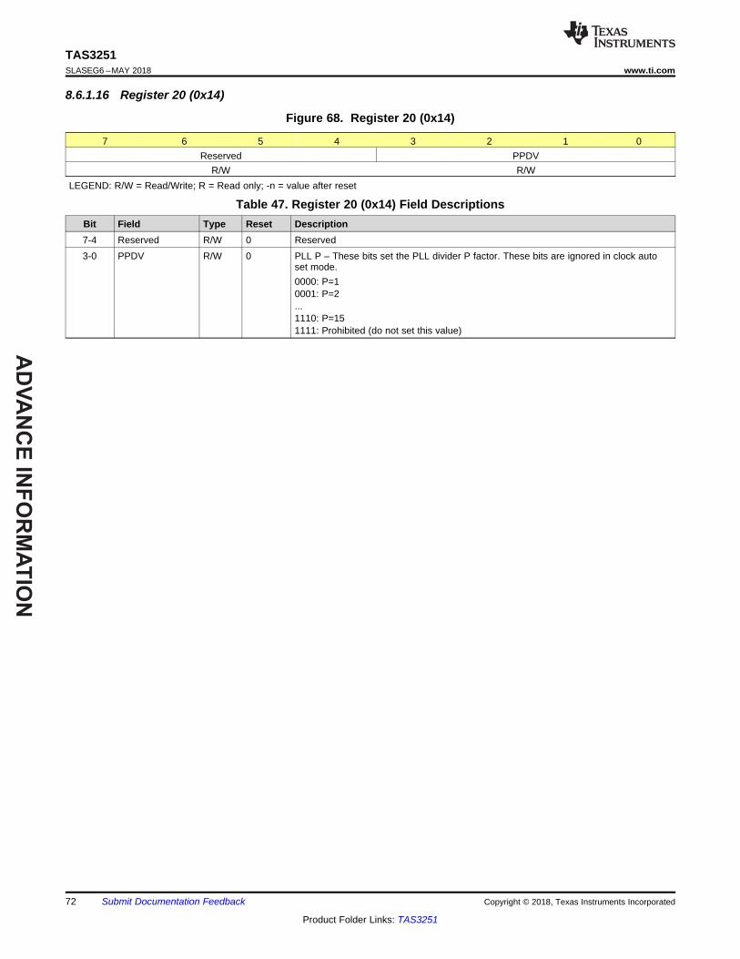
AD
VA
NC
E IN
FO
RM
AT
ION
72
TAS3251SLASEG6 –MAY 2018 www.ti.com
Product Folder Links: TAS3251
Submit Documentation Feedback Copyright © 2018, Texas Instruments Incorporated
8.6.1.16 Register 20 (0x14)
Figure 68. Register 20 (0x14)
7 6 5 4 3 2 1 0Reserved PPDV
R/W R/WLEGEND: R/W = Read/Write; R = Read only; -n = value after reset
Table 47. Register 20 (0x14) Field DescriptionsBit Field Type Reset Description7-4 Reserved R/W 0 Reserved3-0 PPDV R/W 0 PLL P – These bits set the PLL divider P factor. These bits are ignored in clock auto
set mode.0000: P=10001: P=2...1110: P=151111: Prohibited (do not set this value)

AD
VA
NC
E I
NF
OR
MA
TIO
N
73
TAS3251www.ti.com SLASEG6 –MAY 2018
Product Folder Links: TAS3251
Submit Documentation FeedbackCopyright © 2018, Texas Instruments Incorporated
8.6.1.17 Register 21 (0x15)
Figure 69. Register 21 (0x15)
7 6 5 4 3 2 1 0Reserved PJDV
R/W R/WLEGEND: R/W = Read/Write; R = Read only; -n = value after reset
Table 48. Register 21 (0x15) Field DescriptionsBit Field Type Reset Description7-6 Reserved 0 Reserved5-0 PJDV R/W 001000 PLL J – These bits set the J part of the overall PLL multiplication factor J.D * R.
These bits are ignored in clock auto set mode.000000: Prohibited (do not set this value)000001: J=1000010: J=2...111111: J=63
8.6.1.18 Register 22 (0x16)
Figure 70. Register 22 (0x16)
7 6 5 4 3 2 1 0Reserved PDDV
R/W R/WLEGEND: R/W = Read/Write; R = Read only; -n = value after reset
Table 49. Register 22 (0x16) Field DescriptionsBit Field Type Reset Description7-6 Reserved R/W Reserved5-0 PDDV R/W 0 PLL D (MSB) – These bits set the D part of the overall PLL multiplication factor J.D * R.
These bits are ignored in clock auto set mode.0 (in decimal): D=00001 (in decimal): D=0001...9999 (in decimal): D=9999Others: Prohibited (do not set)

AD
VA
NC
E IN
FO
RM
AT
ION
74
TAS3251SLASEG6 –MAY 2018 www.ti.com
Product Folder Links: TAS3251
Submit Documentation Feedback Copyright © 2018, Texas Instruments Incorporated
8.6.1.19 Register 23 (0x17)
Figure 71. Register 23 (0x17)
7 6 5 4 3 2 1 0PDDVR/W
LEGEND: R/W = Read/Write; R = Read only; -n = value after reset
Table 50. Register 23 (0x17) Field DescriptionsBit Field Type Reset Description7-0 PDDV R/W 0 PLL D (LSB) – These bits set the D part of the overall PLL multiplication factor J.D * R.
These bits are ignored in clock auto set mode.0 (in decimal): D=00001 (in decimal): D=0001...9999 (in decimal): D=9999Others: Prohibited (do not set)
8.6.1.20 Register 24 (0x18)
Figure 72. Register 24 (0x18)
7 6 5 4 3 2 1 0Reserved PRDV
R/W R/WLEGEND: R/W = Read/Write; R = Read only; -n = value after reset
Table 51. Register 24 (0x18) Field DescriptionsBit Field Type Reset Description7-4 Reserved R/W Reserved3-0 PRDV R/W 0 PLL R – These bits set the R part of the overall PLL multiplication factor J.D * R. These
bits are ignored in clock auto set mode.0000: R=10001: R=2...1111: R=16
8.6.1.21 Register 27 (0x1B)
Figure 73. Register 27 (0x1B)
7 6 5 4 3 2 1 0Reserved DDSP
R/W R/WLEGEND: R/W = Read/Write; R = Read only; -n = value after reset
Table 52. Register 27 (0x1B) Field DescriptionsBit Field Type Reset Description7 Reserved R/W Reserved
6-0 DDSP R/W 0 DSP Clock Divider – These bits set the source clock divider value for the DSP clock.These bits are ignored in clock auto set mode.0000000: Divide by 10000001: Divide by 2...1111111: Divide by 128

AD
VA
NC
E I
NF
OR
MA
TIO
N
75
TAS3251www.ti.com SLASEG6 –MAY 2018
Product Folder Links: TAS3251
Submit Documentation FeedbackCopyright © 2018, Texas Instruments Incorporated
8.6.1.22 Register 28 (0x1C)
Figure 74. Register 28 (0x1C)
7 6 5 4 3 2 1 0Reserved DDAC
R/W R/WLEGEND: R/W = Read/Write; R = Read only; -n = value after reset
Table 53. Register 28 (0x1C) Field DescriptionsBit Field Type Reset Description7 Reserved Reserved
6-4 DDAC R/W 0 DAC Clock Divider – These bits set the source clock divider value for the DAC clock.These bits are ignored in clock auto set mode.0000000: Divide by 10000001: Divide by 2...1111111: Divide by 128
3-0 R/W 1
8.6.1.23 Register 29 (0x1D)
Figure 75. Register 29 (0x1D)
7 6 5 4 3 2 1 0Reserved DNCP
R/W R/WLEGEND: R/W = Read/Write; R = Read only; -n = value after reset
Table 54. Register 29 (0x1D) Field DescriptionsBit Field Type Reset Description7 Reserved Reserved
6-2 DNCP R/W 0 NCP Clock Divider – These bits set the source clock divider value for the CP clock.These bits are ignored in clock auto set mode.0000000: Divide by 10000001: Divide by 2...1111111: Divide by 128
1-0 R/W 1
8.6.1.24 Register 30 (0x1E)
Figure 76. Register 30 (0x1E)
7 6 5 4 3 2 1 0Reserved DOSR
R/W R/WLEGEND: R/W = Read/Write; R = Read only; -n = value after reset
Table 55. Register 30 (0x1E) Field DescriptionsBit Field Type Reset Description7 Reserved Reserved
6-4 DOSR R/W 0 OSR Clock Divider – These bits set the source clock divider value for the OSR clock.These bits are ignored in clock auto set mode.0000000: Divide by 10000001: Divide by 2...1111111: Divide by 128
3-0 R/W 1

AD
VA
NC
E IN
FO
RM
AT
ION
76
TAS3251SLASEG6 –MAY 2018 www.ti.com
Product Folder Links: TAS3251
Submit Documentation Feedback Copyright © 2018, Texas Instruments Incorporated
8.6.1.25 Register 32 (0x20)
Figure 77. Register 32 (0x20)
7 6 5 4 3 2 1 0Reserved DSCLK
R/W R/WLEGEND: R/W = Read/Write; R = Read only; -n = value after reset
Table 56. Register 32 (0x20) Field DescriptionsBit Field Type Reset Description7 Reserved R/W Reserved
6-0 DSCLK R/W 0 Master Mode SCLK Divider – These bits set the MCLK divider value to generate I2Smaster SCLK clock.0000000: Divide by 10000001: Divide by 2...1111111: Divide by 128
8.6.1.26 Register 33 (0x21)
Figure 78. Register 33 (0x21)
7 6 5 4 3 2 1 0DLRKR/W
LEGEND: R/W = Read/Write; R = Read only; -n = value after reset
Table 57. Register 33 (0x21) Field DescriptionsBit Field Type Reset Description7-0 DLRK R/W 0 Master Mode LRCLK Divider – These bits set the I2S master SCLK clock divider value
to generate I2S master LRCLK clock00000000: Divide by 100000001: Divide by 2...11111111: Divide by 256

AD
VA
NC
E I
NF
OR
MA
TIO
N
77
TAS3251www.ti.com SLASEG6 –MAY 2018
Product Folder Links: TAS3251
Submit Documentation FeedbackCopyright © 2018, Texas Instruments Incorporated
8.6.1.27 Register 34 (0x22)
Figure 79. Register 34 (0x22)
7 6 5 4 3 2 1 0Reserved I16E Reserved FSSP FSSP
R/W R/W R/W R/W R/WLEGEND: R/W = Read/Write; R = Read only; -n = value after reset
Table 58. Register 34 (0x22) Field DescriptionsBit Field Type Reset Description7-5 Reserved R/W Reserved4 I16E R/W 0 16x Interpolation – This bit enables or disables the 16x interpolation mode
0: 8x interpolation1: 16x interpolation
3 Reserved R/W Reserved2 FSSP R/W 1 FS Speed Mode – These bits select the FS operation mode, which must be set
according to the current audio sampling rate. These bits are ignored in clock auto setmode.000: Reserved001: Reserved010: Reserved011: 48 kHz100: 88.2-96 kHz101: Reserved110: Reserved111: 32kHz
1-0 R/W 0

AD
VA
NC
E IN
FO
RM
AT
ION
78
TAS3251SLASEG6 –MAY 2018 www.ti.com
Product Folder Links: TAS3251
Submit Documentation Feedback Copyright © 2018, Texas Instruments Incorporated
8.6.1.28 Register 37 (0x25)
Figure 80. Register 37 (0x25)
7 6 5 4 3 2 1 0Reserved IDFS IDBK IDSK IDCH IDCM DCAS IPLK
R/W R/W R/W R/W R/W R/W R/W R/WLEGEND: R/W = Read/Write; R = Read only; -n = value after reset
Table 59. Register 37 (0x25) Field DescriptionsBit Field Type Reset Description7 Reserved R/W Reserved6 IDFS R/W 0 Ignore FS Detection – This bit controls whether to ignore the FS detection. When
ignored, FS error will not cause a clock error.0: Regard FS detection1: Ignore FS detection
5 IDBK R/W 0 Ignore SCLK Detection – This bit controls whether to ignore the SCLK detectionagainst LRCLK. The SCLK must be stable between 32 FS and 256 FS inclusive or anerror will be reported. When ignored, a SCLK error will not cause a clock error.0: Regard SCLK detection1: Ignore SCLK detection
4 IDSK R/W 0 Ignore MCLK Detection – This bit controls whether to ignore the MCLK detectionagainst LRCLK. Only some certain MCLK ratios within some error margin are allowed.When ignored, an MCLK error will not cause a clock error.0: Regard MCLK detection1: Ignore MCLK detection
3 IDCH R/W 0 Ignore Clock Halt Detection – This bit controls whether to ignore the MCLK halt (staticor frequency is lower than acceptable) detection. When ignored an MCLK halt will notcause a clock error.0: Regard MCLK halt detection1: Ignore MCLK halt detection
2 IDCM R/W 0 Ignore LRCLK/SCLK Missing Detection – This bit controls whether to ignore theLRCLK/SCLK missing detection. The LRCLK/SCLK need to be in low state (not onlystatic) to be deemed missing. When ignored an LRCLK/SCLK missing will not causethe DAC go into powerdown mode.0: Regard LRCLK/SCLK missing detection1: Ignore LRCLK/SCLK missing detection
1 DCAS R/W 0 Disable Clock Divider Autoset – This bit enables or disables the clock auto set mode.When dealing with uncommon audio clock configuration, the auto set mode must bedisabled and all clock dividers must be set manually.Addtionally, some clock detectors might also need to be disabled. The clock autosetfeature will not work with PLL enabled in VCOM mode. In this case this feature has tobe disabled and the clock dividers must be set manually.0: Enable clock auto set1: Disable clock auto set
0 IPLK R/W 0 Ignore PLL Lock Detection – This bit controls whether to ignore the PLL lock detection.When ignored, PLL unlocks will not cause a clock error. The PLL lock flag at P0-R4, bit4 is always correct regardless of this bit.0: PLL unlocks raise clock error1: PLL unlocks are ignored

AD
VA
NC
E I
NF
OR
MA
TIO
N
79
TAS3251www.ti.com SLASEG6 –MAY 2018
Product Folder Links: TAS3251
Submit Documentation FeedbackCopyright © 2018, Texas Instruments Incorporated
8.6.1.29 Register 40 (0x28)
Figure 81. Register 40 (0x28)
7 6 5 4 3 2 1 0Reserved AFMT Reserved ALEN
R/W R/W R/W R/WLEGEND: R/W = Read/Write; R = Read only; -n = value after reset
Table 60. Register 40 (0x28) Field DescriptionsBit Field Type Reset Description7-6 –5-4 AFMT R/W 0 I2S Data Format – These bits control both input and output audio interface formats for
DAC operation.00: I2S01: DSP10: RTJ11: LTJ
3-2 Reserved R/W Reserved1 ALEN R/W 1 I2S Word Length – These bits control both input and output audio interface sample
word lengths for DAC operation.00: 16 bits01: 20 bits10: 24 bits11: 32 bits
0 R/W 0
8.6.1.30 Register 41 (0x29)
Figure 82. Register 41 (0x29)
7 6 5 4 3 2 1 0AOFSR/W
LEGEND: R/W = Read/Write; R = Read only; -n = value after reset
Table 61. Register 41 (0x29) Field DescriptionsBit Field Type Reset Description7-0 AOFS R/W 0 I2S Shift – These bits control the offset of audio data in the audio frame for both input
and output. The offset is defined as the number of SCLK from the starting (MSB) ofaudio frame to the starting of the desired audio sample.00000000: offset = 0 SCLK (no offset)00000001: ofsset = 1 SCLK00000010: offset = 2 SCLKs…11111111: offset = 256 SCLKs

AD
VA
NC
E IN
FO
RM
AT
ION
80
TAS3251SLASEG6 –MAY 2018 www.ti.com
Product Folder Links: TAS3251
Submit Documentation Feedback Copyright © 2018, Texas Instruments Incorporated
8.6.1.31 Register 42 (0x2A)
Figure 83. Register 42 (0x2A)
7 6 5 4 3 2 1 0Reserved AUPL Reserved AUPR
R/W R/W R/W R/WLEGEND: R/W = Read/Write; R = Read only; -n = value after reset
Table 62. Register 42 (0x2A) Field DescriptionsBit Field Type Reset Description7-6 Reserved R/W Reserved5 AUPL R/W 0 Left DAC Data Path – These bits control the left channel audio data path connection.
00: Zero data (mute)01: Left channel data10: Right channel data11: Reserved (do not set)
4 R/W 1
3-2 Reserved R/W Reserved1 AUPR R/W 0 Right DAC Data Path – These bits control the right channel audio data path
connection.00: Zero data (mute)01: Right channel data10: Left channel data11: Reserved (do not set)
0 R/W 1
8.6.1.32 Register 43 (0x2B)
Figure 84. Register 43 (0x2B)
7 6 5 4 3 2 1 0Reserved PSEL
R/W R/WLEGEND: R/W = Read/Write; R = Read only; -n = value after reset
Table 63. Register 43 (0x2B) Field DescriptionsBit Field Type Reset Description7-5 Reserved R/W Reserved4-1 PSEL R/W 0 DSP Program Selection – These bits select the DSP program to use for audio
processing.00000: Reserved00001: Rom Mode 100010: Reserved00011: Reserved
0 R/W 1

AD
VA
NC
E I
NF
OR
MA
TIO
N
81
TAS3251www.ti.com SLASEG6 –MAY 2018
Product Folder Links: TAS3251
Submit Documentation FeedbackCopyright © 2018, Texas Instruments Incorporated
8.6.1.33 Register 44 (0x2C)
Figure 85. Register 44 (0x2C)
7 6 5 4 3 2 1 0Reserved CMDP
R/W R/WLEGEND: R/W = Read/Write; R = Read only; -n = value after reset
Table 64. Register 44 (0x2C) Field DescriptionsBit Field Type Reset Description7-3 Reserved Reserved2-0 CMDP R/W 0 Clock Missing Detection Period – These bits set how long both SCLK and LRCLK keep
low before the audio clocks deemed missing and the DAC transitions to powerdownmode.000: about 1 second001: about 2 seconds010: about 3 seconds...111: about 8 seconds
8.6.1.34 Register 59 (0x3B)
Figure 86. Register 59 (0x3B)
7 6 5 4 3 2 1 0Reserved AMTL Reserved AMTR
R/W R/W R/W R/WLEGEND: R/W = Read/Write; R = Read only; -n = value after reset
Table 65. Register 59 (0x3B) Field DescriptionsBit Field Type Reset Description7 Reserved R/W Reserved
6-4 AMTL R/W 0 Auto Mute Time for Left Channel – These bits specify the length of consecutive zerosamples at left channel before the channel can be auto muted. The times shown arefor 96 kHz sampling rate and will scale with other rates.000: 11.5 ms001: 53 ms010: 106.5 ms011: 266.5 ms100: 0.535 sec101: 1.065 sec110: 2.665 sec111: 5.33 sec
3 Reserved R/W Reserved2-0 AMTR R/W 0 Auto Mute Time for Right Channel – These bits specify the length of consecutive zero
samples at right channel before the channel can be auto muted. The times shown arefor 96 kHz sampling rate and will scale with other rates.000: 11.5 ms001: 53 ms010: 106.5 ms011: 266.5 ms100: 0.535 sec101: 1.065 sec110: 2.665 sec111: 5.33 sec

AD
VA
NC
E IN
FO
RM
AT
ION
82
TAS3251SLASEG6 –MAY 2018 www.ti.com
Product Folder Links: TAS3251
Submit Documentation Feedback Copyright © 2018, Texas Instruments Incorporated
8.6.1.35 Register 60 (0x3C)
Figure 87. Register 60 (0x3C)
7 6 5 4 3 2 1 0Reserved PCTL
R/W R/WLEGEND: R/W = Read/Write; R = Read only; -n = value after reset
Table 66. Register 60 (0x3C) Field DescriptionsBit Field Type Reset Description7-2 Reserved R/W 0 Reserved1-0 PCTL R/W 0 Digital Volume Control – These bits control the behavior of the digital volume.
00: The volume for Left and right channels are independent01: Right channel volume follows left channel setting
8.6.1.36 Register 61 (0x3D)
Figure 88. Register 61 (0x3D)
7 6 5 4 3 2 1 0VOLLR/W
LEGEND: R/W = Read/Write; R = Read only; -n = value after reset
Table 67. Register 61 (0x3D) Field DescriptionsBit Field Type Reset Description7-0 VOLL R/W 00110000 Left Digital Volume – These bits control the left channel digital volume. The
digital volume is 24 dB to –103 dB in –0.5 dB step.00000000: +24.0 dB00000001: +23.5 dB…00101111: +0.5 dB00110000: 0.0 dB00110001: –0.5 dB...11111110: –103 dB11111111: Mute
8.6.1.37 Register 62 (0x3E)
Figure 89. Register 62 (0x3E)
7 6 5 4 3 2 1 0VOLRR/W
LEGEND: R/W = Read/Write; R = Read only; -n = value after reset

AD
VA
NC
E I
NF
OR
MA
TIO
N
83
TAS3251www.ti.com SLASEG6 –MAY 2018
Product Folder Links: TAS3251
Submit Documentation FeedbackCopyright © 2018, Texas Instruments Incorporated
Table 68. Register 62 (0x3E) Field DescriptionsBit Field Type Reset Description7-0 VOLR R/W 0011000
0Right Digital Volume – These bits control the right channel digital volume. The digitalvolume is 24 dB to –103 dB in –0.5 dB step.00000000: +24.0 dB00000001: +23.5 dB…00101111: +0.5 dB00110000: 0.0 dB00110001: –0.5 dB...11111110: –103 dB11111111: Mute
8.6.1.38 Register 63 (0x3F)
Figure 90. Register 63 (0x3F)
7 6 5 4 3 2 1 0VNDF VNDS VNUF VNUSR/W R/W R/W R/W
LEGEND: R/W = Read/Write; R = Read only; -n = value after reset
Table 69. Register 63 (0x3F) Field DescriptionsBit Field Type Reset Description7-6 VNDF R/W 00 Digital Volume Normal Ramp Down Frequency – These bits control the frequency of
the digital volume updates when the volume is ramping down. The setting here isapplied to soft mute request, asserted by XSMUTE pin or P0-R3.00: Update every 1 FS period01: Update every 2 FS periods10: Update every 4 FS periods11: Directly set the volume to zero (Instant mute)
5-4 VNDS R/W 11 Digital Volume Normal Ramp Down Step – These bits control the step of the digitalvolume updates when the volume is ramping down.The setting here is applied to soft mute request, asserted by XSMUTE pin or P0-R3.00: Decrement by 4 dB for each update01: Decrement by 2 dB for each update10: Decrement by 1 dB for each update11: Decrement by 0.5 dB for each update
3-2 VNUF R/W 00 Digital Volume Normal Ramp Up Frequency – These bits control the frequency of thedigital volume updates when the volume is ramping up.The setting here is applied to soft unmute request, asserted by XSMUTE pin or P0-R3.00: Update every 1 FS period01: Update every 2 FS periods10: Update every 4 FS periods11: Directly restore the volume (Instant unmute)
1-0 VNUS R/W 11 Digital Volume Normal Ramp Up Step – These bits control the step of the digitalvolume updates when the volume is ramping up.The setting here is applied to soft unmute request, asserted by XSMUTE pin or P0-R3.00: Increment by 4 dB for each update01: Increment by 2 dB for each update10: Increment by 1 dB for each update11: Increment by 0.5 dB for each update

AD
VA
NC
E IN
FO
RM
AT
ION
84
TAS3251SLASEG6 –MAY 2018 www.ti.com
Product Folder Links: TAS3251
Submit Documentation Feedback Copyright © 2018, Texas Instruments Incorporated
8.6.1.39 Register 64 (0x40)
Figure 91. Register 64 (0x40)
7 6 5 4 3 2 1 0VEDF VEDS ReservedR/W R/W R/W
LEGEND: R/W = Read/Write; R = Read only; -n = value after reset
Table 70. Register 64 (0x40) Field DescriptionsBit Field Type Reset Description7-6 VEDF R/W 0 Digital Volume Emergency Ramp Down Frequency – These bits control the frequency
of the digital volume updates when the volume is ramping down due to clock error orpower outage, which usually needs faster ramp down compared to normal soft mute.00: Update every 1 FS period01: Update every 2 FS periods10: Update every 4 FS periods11: Directly set the volume to zero (Instant mute)
5-4 VEDS R/W 1 Digital Volume Emergency Ramp Down Step – These bits control the step of the digitalvolume updates when the volume is ramping down due to clock error or power outage,which usually needs faster ramp down compared to normal soft mute.00: Decrement by 4 dB for each update01: Decrement by 2 dB for each update10: Decrement by 1 dB for each update11: Decrement by 0.5 dB for each update
3-0 Reserved R/W Reserved
8.6.1.40 Register 65 (0x41)
Figure 92. Register 65 (0x41)
7 6 5 4 3 2 1 0Reserved ACTL AMLE AMRE
R/W R/W R/W R/WLEGEND: R/W = Read/Write; R = Read only; -n = value after reset
Table 71. Register 65 (0x41) Field DescriptionsBit Field Type Reset Description7-3 Reserved R/W Reserved2 ACTL R/W 1 Auto Mute Control**NOBUS** – This bit controls the behavior of the auto mute upon
zero sample detection. The time length for zero detection is set with P0-R59.0: Auto mute left channel and right channel independently.1: Auto mute left and right channels only when both channels are about to be automuted.
1 AMLE R/W 1 Auto Mute Left Channel**NOBUS** – This bit enables or disables auto mute on rightchannel. Note that when right channel auto mute is disabled and the P0-R65, bit 2 isset to 1, the left channel will also never be auto muted.0: Disable right channel auto mute1: Enable right channel auto mute
0 AMRE R/W 1 Auto Mute Right Channel**NOBUS** – This bit enables or disables auto mute on leftchannel. Note that when left channel auto mute is disabled and the P0-R65, bit 2 is setto 1, the right channel will also never be auto muted.0: Disable left channel auto mute1: Enable left channel auto mute

AD
VA
NC
E I
NF
OR
MA
TIO
N
85
TAS3251www.ti.com SLASEG6 –MAY 2018
Product Folder Links: TAS3251
Submit Documentation FeedbackCopyright © 2018, Texas Instruments Incorporated
8.6.1.41 Register 67 (0x43)
Figure 93. Register 67 (0x43)
7 6 5 4 3 2 1 0DLPA DRPA DLPM DRPMR/W R/W R/W R/W
LEGEND: R/W = Read/Write; R = Read only; -n = value after reset
Table 72. Register 67 (0x43) Field DescriptionsBit Field Type Reset Description7-6 DLPA R/W 0 Left DAC primary AC dither gain – These bits control the AC dither gain for left channel
primary DAC modulator.00: AC dither gain = 0.12501: AC dither gain = 0.25
5-4 DRPA R/W 0 Right DAC primary AC dither gain – These bits control the AC dither gain for rightchannel primary DAC modulator.00: AC dither gain = 0.12501: AC dither gain = 0.25
3-2 DLPM R/W 0 Left DAC primary DEM dither gain – These bits control the dither gain for left channelprimary Galton DEM.00: DEM dither gain = 0.501: DEM dither gain = 1.0Others: Reserved (do not set)
1-0 DRPM R/W 0 Right DAC primary DEM dither gain – These bits control the dither gain for rightchannel primary Galton DEM.00: DEM dither gain = 0.501: DEM dither gain = 1.0Others: Reserved (do not set)
8.6.1.42 Register 68 (0x44)
Figure 94. Register 68 (0x44)
7 6 5 4 3 2 1 0Reserved DLPD
R/W R/WLEGEND: R/W = Read/Write; R = Read only; -n = value after reset
Table 73. Register 68 (0x44) Field DescriptionsBit Field Type Reset Description7-3 Reserved R/W Reserved2-0 DLPD R/W 0 Left DAC primary DC dither – These bits control the DC dither amount to be added to
the lower part of the left channel primary DAC modulator. The DC dither is expressedis Q0.11 format, with 1.0 equals to 1/32 fullscale modulator input.00000000000 : No DC dither00000000001 : 2-11 × 1/32 FS00000000010 : 2-10 × 1/32 FS

AD
VA
NC
E IN
FO
RM
AT
ION
86
TAS3251SLASEG6 –MAY 2018 www.ti.com
Product Folder Links: TAS3251
Submit Documentation Feedback Copyright © 2018, Texas Instruments Incorporated
8.6.1.43 Register 69 (0x45)
Figure 95. Register 69 (0x45)
7 6 5 4 3 2 1 0DLPDR/W
LEGEND: R/W = Read/Write; R = Read only; -n = value after reset
Table 74. Register 69 (0x45) Field DescriptionsBit Field Type Reset Description7-0 DLPD R/W 0 Left DAC primary DC dither – These bits control the DC dither amount to be added to
the lower part of the left channel primary DAC modulator. The DC dither is expressedis Q0.11 format, with 1.0 equals to 1/32 fullscale modulator input.00000000000 : No DC dither00000000001 : 2-11 × 1/32 FS00000000010 : 2-10 × 1/32 FS
8.6.1.44 Register 70 (0x46)
Figure 96. Register 70 (0x46)
7 6 5 4 3 2 1 0DRPDR/W
LEGEND: R/W = Read/Write; R = Read only; -n = value after reset
Table 75. Register 70 (0x46) Field DescriptionsBit Field Type Reset Description7-0 DRPD R/W 0 Right DAC primary DC dither – These bits control the DC dither amount to be added to
the lower part of the right channel primary DAC modulator. The DC dither is expressedis Q0.11 format, with 1.0 equals to 1/32 fullscale modulator input.00000000000 : No DC dither00000000001 : 2-11 × 1/32 FS00000000010 : 2-10 × 1/32 FS
8.6.1.45 Register 71 (0x47)
Figure 97. Register 71 (0x47)
7 6 5 4 3 2 1 0DRPDR/W
LEGEND: R/W = Read/Write; R = Read only; -n = value after reset
Table 76. Register 71 (0x47) Field DescriptionsBit Field Type Reset Description7-0 DRPD R/W 0 Right DAC primary DC dither – These bits control the DC dither amount to be added to
the lower part of the right channel primary DAC modulator. The DC dither is expressedis Q0.11 format, with 1.0 equals to 1/32 fullscale modulator input.00000000000 : No DC dither00000000001 : 2-11 × 1/32 FS00000000010 : 2-10 × 1/32 FS

AD
VA
NC
E I
NF
OR
MA
TIO
N
87
TAS3251www.ti.com SLASEG6 –MAY 2018
Product Folder Links: TAS3251
Submit Documentation FeedbackCopyright © 2018, Texas Instruments Incorporated
8.6.1.46 Register 72 (0x48)
Figure 98. Register 72 (0x48)
7 6 5 4 3 2 1 0DLSA DRSA DLSM RSMR/W R/W R/W R/W
LEGEND: R/W = Read/Write; R = Read only; -n = value after reset
Table 77. Register 72 (0x48) Field DescriptionsBit Field Type Reset Description7-6 DLSA R/W 01 Left DAC secondary AC dither gain – These bits control the AC dither gain for left
channel secondary DAC.00: AC dither gain = 0.12501: AC dither gain = 0.25
5-4 DRSA R/W 01 Right DAC secondary AC dither gain – These bits control the AC dither gain for rightchannel secondary DAC modulator.00: AC dither gain = 0.12501: AC dither gain = 0.2510: AC dither gain = 0.511: no AC dither
3-2 DLSM R/W 01 Left DAC secondary DEM dither gain – These bits control the dither gain for leftchannel secondary Galton DEM.00: DEM dither gain = 0.501: DEM dither gain = 1.0Others: Reserved (do not set)
1-0 DRSM R/W 01 Right DAC secondary DEM dither gain – These bits control the dither gain for rightchannel secondary Galton DEM.00: DEM dither gain = 0.501: DEM dither gain = 1.0Others: Reserved (do not set)

AD
VA
NC
E IN
FO
RM
AT
ION
88
TAS3251SLASEG6 –MAY 2018 www.ti.com
Product Folder Links: TAS3251
Submit Documentation Feedback Copyright © 2018, Texas Instruments Incorporated
8.6.1.47 Register 73 (0x49)
Figure 99. Register 73 (0x49)
7 6 5 4 3 2 1 0DLSDR/W
LEGEND: R/W = Read/Write; R = Read only; -n = value after reset
Table 78. Register 73 (0x49) Field DescriptionsBit Field Type Reset Description7-0 DLSD R/W 0 Left DAC secondary DC dither – These bits control the DC dither amount to be added
to the lower part of the left channel secondary DAC modulator. The DC dither isexpressed is Q0.11 format, with 1.0 equals to 1/32 fullscale modulator input.00000000000 : No DC dither00000000001 : 2–11 × 1/32 FS00000000010 : 2–10 × 1/32 FS
8.6.1.48 Register 74 (0x4A)
Figure 100. Register 74 (0x4A)
7 6 5 4 3 2 1 0DLSDR/W
LEGEND: R/W = Read/Write; R = Read only; -n = value after reset
Table 79. Register 74 (0x4A) Field DescriptionsBit Field Type Reset Description7-0 DLSD R/W 0 Left DAC secondary DC dither – These bits control the DC dither amount to be added
to the lower part of the left channel secondary DAC modulator. The DC dither isexpressed is Q0.11 format, with 1.0 equals to 1/32 fullscale modulator input.00000000000 : No DC dither00000000001 : 2–11 × 1/32 FS00000000010 : 2–10 × 1/32 FS

AD
VA
NC
E I
NF
OR
MA
TIO
N
89
TAS3251www.ti.com SLASEG6 –MAY 2018
Product Folder Links: TAS3251
Submit Documentation FeedbackCopyright © 2018, Texas Instruments Incorporated
8.6.1.49 Register 75 (0x4B)
Figure 101. Register 75 (0x4B)
7 6 5 4 3 2 1 0DRSDR/W
LEGEND: R/W = Read/Write; R = Read only; -n = value after reset
Table 80. Register 75 (0x4B) Field DescriptionsBit Field Type Reset Description7-0 DRSD R/W 0000000
0Right DAC secondary DC dither – These bits control the DC dither amount to be addedto the lower part of the right channel secondary DAC modulator. The DC dither isexpressed is Q0.11 format, with 1.0 equals to 1/32 fullscale modulator input.00000000000 : No DC dither00000000001 : 2–11 × 1/32 FS00000000010 : 2–10 × 1/32 FS
8.6.1.50 Register 76 (0x4C)
Figure 102. Register 76 (0x4C)
7 6 5 4 3 2 1 0DRSDR/W
LEGEND: R/W = Read/Write; R = Read only; -n = value after reset
Table 81. Register 76 (0x4C) Field DescriptionsBit Field Type Reset Description7-0 DRSD R/W 0000000
0Right DAC secondary DC dither – These bits control the DC dither amount to be addedto the lower part of the right channel secondary DAC modulator. The DC dither isexpressed is Q0.11 format, with 1.0 equals to 1/32 fullscale modulator input.00000000000 : No DC dither00000000001 : 2–11 × 1/32 FS00000000010 : 2–10 × 1/32 FS

AD
VA
NC
E IN
FO
RM
AT
ION
90
TAS3251SLASEG6 –MAY 2018 www.ti.com
Product Folder Links: TAS3251
Submit Documentation Feedback Copyright © 2018, Texas Instruments Incorporated
8.6.1.51 Register 78 (0x4E)
Figure 103. Register 78 (0x4E)
7 6 5 4 3 2 1 0OLOFR/W
LEGEND: R/W = Read/Write; R = Read only; -n = value after reset
Table 82. Register 78 (0x4E) Field DescriptionsBit Field Type Reset Description7-0 OLOF R/W 0000000
0Left OFSCAL offset – These bits controls the amount of manual DC offset to be addedto the left channel DAC output. The additional offset would be approximately thenegative of the decimal value of this register divided by 4 in mV.01111111 : –31.75 mV01111110 : –31.50 mV…00000010 : –0.50 mV00000001 : –0.25 mV00000000 : 0.0 mV11111111 : +0.25 mV11111110 : +0.50 mV…10000000 : +32.0 mV
8.6.1.52 Register 79 (0x4F)
Figure 104. Register 79 (0x4F)
7 6 5 4 3 2 1 0OROF
R/W R/W R/W R/W R/W R/W R/W R/WLEGEND: R/W = Read/Write; R = Read only; -n = value after reset
Table 83. Register 79 (0x4F) Field DescriptionsBit Field Type Reset Description7-0 OROF R/W 0 Right OFSCAL offset – These bits controls the amount of manual DC offset to be
added to the right channel DAC output. The additional offset would be approximatelythe negative of the decimal value of this register divided by 4 in mV.01111111 : –31.75 mV01111110 : –31.50 mV…00000010 : –0.50 mV00000001 : –0.25 mV00000000 : 0.0 mV11111111 : +0.25 mV11111110 : +0.50 mV…10000000 : +32.0 mV

AD
VA
NC
E I
NF
OR
MA
TIO
N
91
TAS3251www.ti.com SLASEG6 –MAY 2018
Product Folder Links: TAS3251
Submit Documentation FeedbackCopyright © 2018, Texas Instruments Incorporated
8.6.1.53 Register 85 (0x55)
Figure 105. Register 85 (0x55)
7 6 5 4 3 2 1 0Reserved G2SL
R/W R/WLEGEND: R/W = Read/Write; R = Read only; -n = value after reset
Table 84. Register 85 (0x55) Register Field DescriptionsBit Field Type Reset Description7-5 Reserved R/W 0 Reserved4-0 G2SL R/W 0 SDOUT Output Selection – These bits select the signal to output to SDOUT. To
actually output the selected signal, the SDOUT must be set to output mode at P0-R8.0000: off (low)0001: DSP SDOUT output0010: Register SDOUT output (P0-R86, bit 5)0011: Auto mute flag (asserted when both L and R channels are auto muted)0100: Auto mute flag for left channel0101: Auto mute flag for right channel0110: Clock invalid flag (clock error or clock changing or clock missing)0111: Serial audio interface data output (SDOUT)1000: Analog mute flag for left channel (low active)1001: Analog mute flag for right channel (low active)1010: PLL lock flag1011: Charge pump clock1100: Reserved1101: Reserved1110: Under voltage flag, asserted when XSMUTE voltage is higher than 0.7 DVDD1111: Under voltage flag, asserted when XSMUTE voltage is higher than 0.3 DVDD **INTERNAL **1100: Short detection flag for left channel1101: Short detection flag for right channel10000: PLL clock/4 10001: Oscillator clock/410010: Impedance sense flag for left channel10011: Impedance sense flag for right channel10100: Internal UVP flag, becomes low when VDD falls below roughly 2.7V10101: Offset calibration flag, asserted when the system is offset calibrating itself.10110: Clock error flag10111: Clock changing flag11000: Clock missing flag11001: Clock halt detection flag11010: DSP boot done flag11011: Charge pump voltage output valid flag (low active)Others: N/A (zero)

AD
VA
NC
E IN
FO
RM
AT
ION
92
TAS3251SLASEG6 –MAY 2018 www.ti.com
Product Folder Links: TAS3251
Submit Documentation Feedback Copyright © 2018, Texas Instruments Incorporated
8.6.1.54 Register 86 (0x56)
Figure 106. Register 86 (0x56)
7 6 5 4 3 2 1 0R/W R/W R/W R/W
LEGEND: R/W = Read/Write; R = Read only; -n = value after reset
Table 85. Register 86 (0x56) Register Field DescriptionsBit Field Type Reset Description7-6 Reserved R/W 0 Reserved5 GOUT2 R/W 0 GPIO Output Control – This bit controls the SDOUT pin output when the selection at
P0-R85 is set to 0010 (register output)0: Output low1: Output high
4 MUTE R/W 0 This bit controls the MUTE output when the selection at P0-R84 is set to 0010 (registeroutput).0: Output low1: Output high
3-0 Reserved R/W 0 Reserved
8.6.1.55 Register 87 (0x57)
Figure 107. Register 87 (0x57)
7 6 5 4 3 2 1 0R/W R/W R/W R/W
LEGEND: R/W = Read/Write; R = Read only; -n = value after reset
Table 86. Register 87 (0x57) Field DescriptionsBit Field Type Reset Description7-6 Reserved R/W 0 Reserved5 GINV2 R/W 0 GPIO Output Inversion – This bit controls the polarity of the SDOUT pin output. When
set to 1, the output will be inverted for any signal being selected.0: Non-inverted1: Inverted
4 MUTE R/W 0 This bit controls the polarity of MUTE output. When set to 1, the output will be invertedfor any signal being selected.0: Non-inverted1: Inverted
3-0 Reserved R/W 0 Reserved
8.6.1.56 Register 88 (0x58)
Figure 108. Register 88 (0x58)
7 6 5 4 3 2 1 0DIEI
RLEGEND: R/W = Read/Write; R = Read only; -n = value after reset
Table 87. Register 88 (0x58) Field DescriptionsBit Field Type Reset Description7-0 DIEI RO 0x84 Die ID, Device ID = 0x84

AD
VA
NC
E I
NF
OR
MA
TIO
N
93
TAS3251www.ti.com SLASEG6 –MAY 2018
Product Folder Links: TAS3251
Submit Documentation FeedbackCopyright © 2018, Texas Instruments Incorporated
8.6.1.57 Register 91 (0x5B)
Figure 109. Register 91 (0x5B)
7 6 5 4 3 2 1 0Reserved DTFS DTSR
R/W R RLEGEND: R/W = Read/Write; R = Read only; -n = value after reset
Table 88. Register 91 (0x5B) Field DescriptionsBit Field Type Reset Description7 Reserved R/W 0 Reserved
6-4 DTFS R 0 Detected FS – These bits indicate the currently detected audio sampling rate.000: Error (Out of valid range)001: 8 kHz010: 16 kHz011: 32-48 kHz100: 88.2-96 kHz101: 176.4-192 kHz110: 384 kHz
3-0 DTSR R 0 Detected MCLK Ratio – These bits indicate the currently detected MCLK ratio. Notethat even if the MCLK ratio is not indicated as error, clock error might still be flaggeddue to incompatible combination with the sampling rate. Specifically the MCLK ratiomust be high enough to allow enough DSP cycles for minimal audio processing whenPLL is disabled. The absolute MCLK frequency must also be lower than 50 MHz.0000: Ratio error (The MCLK ratio is not allowed)0001: MCLK = 32 FS0010: MCLK = 48 FS0011: MCLK = 64 FS0100: MCLK = 128 FS0101: MCLK = 192 FS0110: MCLK = 256 FS0111: MCLK = 384 FS1000: MCLK = 512 FS1001: MCLK = 768 FS1010: MCLK = 1024 FS1011: MCLK = 1152 FS1100: MCLK = 1536 FS1101: MCLK = 2048 FS1110: MCLK = 3072 FS

AD
VA
NC
E IN
FO
RM
AT
ION
94
TAS3251SLASEG6 –MAY 2018 www.ti.com
Product Folder Links: TAS3251
Submit Documentation Feedback Copyright © 2018, Texas Instruments Incorporated
8.6.1.58 Register 92 (0x5C)
Figure 110. Register 92 (0x5C)
7 6 5 4 3 2 1 0Reserved DTBR
R/W RLEGEND: R/W = Read/Write; R = Read only; -n = value after reset
Table 89. Register 92 (0x5C) Field DescriptionsBit Field Type Reset Description7-1 Reserved R/W 0 Reserved0 DTBR R 0 Detected SCLK Ratio (MSB)
8.6.1.59 Register 93 (0x5D)
Figure 111. Register 93 (0x5D)
7 6 5 4 3 2 1 0DTBRR/W
LEGEND: R/W = Read/Write; R = Read only; -n = value after reset
Table 90. Register 93 (0x5D) Field DescriptionsBit Field Type Reset Description7-0 DTBR R/W Detected SCLK Ratio (LSB) – These bits indicate the currently detected SCLK
ratio, i.e. the number of SCLK clocks in one audio frame. Note that for extremecase of SCLK = 1 FS (which is not usable anyway), the detected ratio will beunreliable

AD
VA
NC
E I
NF
OR
MA
TIO
N
95
TAS3251www.ti.com SLASEG6 –MAY 2018
Product Folder Links: TAS3251
Submit Documentation FeedbackCopyright © 2018, Texas Instruments Incorporated
8.6.1.60 Register 94 (0x5E)
Figure 112. Register 94 (0x5E)
7 6 5 4 3 2 1 0Reserved CDST6 CDST5 CDST4 CDST3 CDST2 CDST1 CDST0
R/W R R R R R R RLEGEND: R/W = Read/Write; R = Read only; -n = value after reset
Table 91. Register 94 (0x5E) Field DescriptionsBit Field Type Reset Description7 Reserved R/W 0 Reserved6 CDST6 R Clock Detector Status – This bit indicates whether the MCLK clock is present or not.
0: MCLK is present1: MCLK is missing (halted)
5 CDST5 R This bit indicates whether the PLL is locked or not. The PLL will be reported asunlocked when it is disabled.0: PLL is locked1: PLL is unlocked
4 CDST4 R This bit indicates whether the both LRCLK and SCLK are missing (tied low) or not.0: LRCLK and/or SCLK is present 1: LRCLK and SCLK are missing
3 CDST3 R This bit indicates whether the combination of current sampling rate and MCLK ratio isvalid for clock auto set.0: The combination of FS/MCLK ratio is valid1: Error (clock auto set is not possible)
2 CDST2 R This bit indicates whether the MCLK is valid or not. The MCLK ratio must be detectableto be valid. There is a limitation with this flag, that is, when the low period of LRCLK isless than or equal to five SCLKs, this flag will be asserted (MCLK invalid reported).0: MCLK is valid1: MCLK is invalid
1 CDST1 R This bit indicates whether the SCLK is valid or not. The SCLK ratio must be stable andin the range of 32-256FS to be valid.0: SCLK is valid1: SCLK is invalid
0 CDST0 R This bit indicated whether the audio sampling rate is valid or not. The sampling ratemust be detectable to be valid. There is a limitation with this flag, that is when this flagis asserted and P0-R37 is set to ignore all asserted error flags such that the DACrecovers, this flag will be de-asserted (sampling rate invalid not reported anymore).0: Sampling rate is valid1: Sampling rate is invalid

AD
VA
NC
E IN
FO
RM
AT
ION
96
TAS3251SLASEG6 –MAY 2018 www.ti.com
Product Folder Links: TAS3251
Submit Documentation Feedback Copyright © 2018, Texas Instruments Incorporated
8.6.1.61 Register 95 (0x5F)
Figure 113. Register 95 (0x5F)
7 6 5 4 3 2 1 0Reserved LTSH Reserved CKMF CSRF CERF
R/W R R/W R R RLEGEND: R/W = Read/Write; R = Read only; -n = value after reset
Table 92. Register 95 (0x5F) Field DescriptionsBit Field Type Reset Description7-5 Reserved R/W 0 Reserved4 LTSH R Latched Clock Halt – This bit indicates whether MCLK halt has occurred. The bit is
cleared when read.0: MCLK halt has not occurred1: MCLK halt has occurred since last read
3 Reserved R/W 0 Reserved2 CKMF R Clock Missing – This bit indicates whether the LRCLK and SCLK are missing (tied low).
0: LRCLK and/or SCLK is present1: LRCLK and SCLK are missing
1 CSRF R Clock Resync Request – This bit indicates whether the clock resynchronization is inprogress.0: Not resynchronizing1: Clock resynchronization is in progress
0 CERF R Clock Error – This bit indicates whether a clock error has occurred. The bit is clearedwhen read0: Clock error has not occurred1: Clock error has occurred.

AD
VA
NC
E I
NF
OR
MA
TIO
N
97
TAS3251www.ti.com SLASEG6 –MAY 2018
Product Folder Links: TAS3251
Submit Documentation FeedbackCopyright © 2018, Texas Instruments Incorporated
8.6.1.62 Register 108 (0x6C)
Figure 114. Register 108 (0x6C)
7 6 5 4 3 2 1 0Reserved AMLM AMRM
R/W R RLEGEND: R/W = Read/Write; R = Read only; -n = value after reset
Table 93. Register 108 (0x6C) Field DescriptionsBit Field Type Reset Description7-2 Reserved R/W 0 Reserved1 AMLM R Left Analog Mute Monitor – This bit is a monitor for left channel analog mute status.
0: Mute1: Unmute
0 AMRM R Right Analog Mute Monitor – This bit is a monitor for right channel analog mute status.0: Mute1: Unmute
8.6.1.63 Register 119 (0x77)
Figure 115. Register 119 (0x77)
7 6 5 4 3 2 1 0Reserved GPIN2 MUTE Reserved
R/W R R RLEGEND: R/W = Read/Write; R = Read only; -n = value after reset
Table 94. Register 119 (0x77) Field DescriptionsBit Field Type Reset Description7-6 Reserved R/W 0 Reserved5 GPIN2 R 0 GPIO Input States – This bit indicates the logic level at SDOUT pin.
0: Low1: High
4 MUTE R 0 This bit indicates the logic level at MUTE pin.0: Low1: High
3-0 Reserved R 0 Reserved bits. Data on these bits may vary.0: Low1: High

AD
VA
NC
E IN
FO
RM
AT
ION
98
TAS3251SLASEG6 –MAY 2018 www.ti.com
Product Folder Links: TAS3251
Submit Documentation Feedback Copyright © 2018, Texas Instruments Incorporated
8.6.1.64 Register 120 (0x78)
Figure 116. Register 120 (0x78)
7 6 5 4 3 2 1 0Reserved AMFL Reserved AMFR
R/W R R/W RLEGEND: R/W = Read/Write; R = Read only; -n = value after reset
Table 95. Register 120 (0x78) Field DescriptionsBit Field Type Reset Description7-5 Reserved R/W 0 Reserved4 AMFL R Auto Mute Flag for Left Channel – This bit indicates the auto mute status for left
channel.0: Not auto muted1: Auto muted
3-1 Reserved R/W 0 Reserved0 AMFR R Auto Mute Flag for Right Channel – This bit indicates the auto mute status for right
channel.0: Not auto muted1: Auto muted
8.6.2 Registers - Page 1
8.6.2.1 Register 1 (0x01)
Figure 117. Register 1 (0x01)
7 6 5 4 3 2 1 0Reserved OSEL
R/W R/WLEGEND: R/W = Read/Write; R = Read only; -n = value after reset
Table 96. Register 1 (0x01) Field DescriptionsBit Field Type Reset Description7-1 Reserved R/W 0 Reserved
0 OSEL R/W 0
Output Amplitude Type - This bit selects the output amplitude type. The clock autosetfeature will not work with PLL enabled in VCOM mode.In this case this feature has to be disabled via P0-R37 and the clock dividers must beset manually.0: VREF mode (Constant output amplitude against AVDD variation)1: VCOM mode (Output amplitude is proportional to AVDD variation)

AD
VA
NC
E I
NF
OR
MA
TIO
N
99
TAS3251www.ti.com SLASEG6 –MAY 2018
Product Folder Links: TAS3251
Submit Documentation FeedbackCopyright © 2018, Texas Instruments Incorporated
8.6.2.2 Register 2 (0x02)
Figure 118. Register 2 (0x02)
7 6 5 4 3 2 1 0Reserved LAGN Reserved RAGN
R/W R/W R/W R/WLEGEND: R/W = Read/Write; R = Read only; -n = value after reset
Table 97. Register 2 (0x02) Field DescriptionsBit Field Type Reset Description7-5 Reserved R/W 0 Reserved
4 LAGN R/W 0Analog Gain Control for Left Channel - This bit controls the left channel analog gain.0: 0 dB1: -6 dB
3-1 Reserved R/W 0 Reserved
0 RAGN R/W 0Analog Gain Control for Right Channel - This bit controls the right channel analog gain.0: 0 dB1: -6 dB
8.6.2.3 Register 6 (0x06)
Figure 119. Register 6 (0x06)
7 6 5 4 3 2 1 0Reserved AMCT
R/W R/WLEGEND: R/W = Read/Write; R = Read only; -n = value after reset
Table 98. Register 6 (0x06) Field DescriptionsBit Field Type Reset Description7-1 Reserved R/W 0 Reserved
0 AMCT R/W 1Analog Mute Control -This bit enables or disables analog mute following digital mute.0: Disabled1: Enabled

AD
VA
NC
E IN
FO
RM
AT
ION
100
TAS3251SLASEG6 –MAY 2018 www.ti.com
Product Folder Links: TAS3251
Submit Documentation Feedback Copyright © 2018, Texas Instruments Incorporated
8.6.2.4 Register 7 (0x07)
Figure 120. Register 7 (0x07)
7 6 5 4 3 2 1 0Reserved AGBL Reserved AGBR
R/W R/W R/W R/WLEGEND: R/W = Read/Write; R = Read only; -n = value after reset
Table 99. Register 7 (0x07) Field DescriptionsBit Field Type Reset Description7-5 Reserved R/W 0 Reserved
4 AGBL R/W 0
Analog +10% Gain for Left Channel - This bit enables or disables amplitude boostmode for left channel.0: Normal amplitude1: +10% (+0.8 dB) boosted amplitude
3-1 Reserved R/W 0 Reserved
0 AGBR R/W 0
Analog +10% Gain for Right Channel - This bit enables or disables amplitude boostmode for right channel.0: Normal amplitude1: +10% (+0.8 dB) boosted amplitude
8.6.2.5 Register 9 (0x09)
Figure 121. Register 9 (0x09)
7 6 5 4 3 2 1 0Reserved DEME VCPD
R/W R/W R/WLEGEND: R/W = Read/Write; R = Read only; -n = value after reset
Table 100. Register 9 (0x09) Field DescriptionsBit Field Type Reset Description7-2 Reserved R/W 0 Reserved
1 DEME R/W 0
VCOM Pin as De-emphasis Control - This bit controls whether to use theDEEMP/VCOM pin as De-emphasis control.0: Disabled (DEEMP/VCOM is not used to control De-emphasis)1: Enabled (DEEMP/VCOM is used to control De-emphasis)
0 VCPD R/W 1Power down control for VCOM - This bit controls VCOM powerdown switch.0: VCOM is powered on1: VCOM is powered down

AD
VA
NC
E I
NF
OR
MA
TIO
N
101
TAS3251www.ti.com SLASEG6 –MAY 2018
Product Folder Links: TAS3251
Submit Documentation FeedbackCopyright © 2018, Texas Instruments Incorporated
9 Application and Implementation
NOTEInformation in the following applications sections is not part of the TI componentspecification, and TI does not warrant its accuracy or completeness. TI’s customers areresponsible for determining suitability of components for their purposes. Customers shouldvalidate and test their design implementation to confirm system functionality.
9.1 Typical ApplicationsThe TAS3251 device supports both 2-channel, bridge-tied load (BTL) and mono, parallel bridge-tied load outputconfigurations. This allows flexibility to configure and program the device for a number of different applications:
• 2.0, Stereo Systems - this is a standard stereo configuration. Use either one TAS3251 device in stereo, BTLor two TTAS3251 devices in PBTL.
• 0.1, Mono Speaker - the TAS3251 can be used as a 1-channel amplifier when configured in PBTL.• Two-Way (1.1) Powered Speaker - the TAS3251 processing and amplifier support two-way or active
crossover systems with a tweeter and woofer driven by independent amplifiers. This allows for the removal ofpassive crossover components in the speaker. This can either be accomplished using one TAS3251 device inBTL or two TAS3251 devices in PBTL.
• Three-Way Powered Speaker - the TAS3251 processing and amplifier support a three-way active speakerwith a tweeter, mid-range and woofer each driven by independent amplifiers. This allows the removal ofpassive crossover components in the speaker. This can be accomplished by using two TAS3251 devices (2xBTL + 1x PBTL) or three TAS3251 devices each configured in PBTL.
• 2.1 Systems - the TAS3251 can be configured to support a 2.1 to support stereo, 2-channels (2x BTL) and asubwoofer (1x PBTL).

AD
VA
NC
E IN
FO
RM
AT
ION
TAS3251
2DAC_OUTB-
1DAC_OUTB+
3DAC_OUTA-
4DAC_OUTA+
5CPVSS
6CN
8CP
7GND
9DAC_DVDD
10DGND
11DVDD_REG
12GVDD_A
14MODE
13GND
15SPK_INA+
16SPK_INA-
17OC_ADJ
18FREQ_ADJ
20OSC_IOP
19OSC_IOM
21DVDD
22GND
23AVDD
24C_START
26SPK_INB-
25SPK_INB+
27
28
55AGND
56DAC_AVDD
54SDA
53SCL
52XPU
51SDOUT
49SCLK
50MCLK
48SDIN
47LRCK
46ADR
45
43BST_A-
44BST_A+
42GND
41SPK_OUTA+
40PVDD_A
39SPK_OUTA-
37GND
38GND
36SPK_OUTB+
35PVDD_B
34SPK_OUTB-
33GND
31BST_B-
32BST_B+
30GVDD_B
29CLIP_OTW
DAC_MUTE
FAULT
RESET_AMP
LFILTER
LFILTER
LFILTER
LFILTER
33nF
PVDD
GND
MCLK
SDOUT
SDA SCL
/CLIP_OTW
/DAC_MUTE
/FAULT
3.3 V
12V
3.3 V
10 k 10 k
3.3 V
1 F
1 F
10 nF
RFREQ_ADJ
ROC_ADJ
10 F
10 F
330 nF
1 µF
1 F
1 F
1 F
10 µF
10 µF
33 nF
1 F
470 F
CFILTER
CFILTER
33 nF
100 nF
33 nF
CFILTER
CFILTER
/RESET_AMP
SCLK
SDIN
LRCLK
1 F
12 V
1 F 470 PF
499
499
100 k 100 k
1 nF
499
499
1 nF
100 k 100 k
102
TAS3251SLASEG6 –MAY 2018 www.ti.com
Product Folder Links: TAS3251
Submit Documentation Feedback Copyright © 2018, Texas Instruments Incorporated
Typical Applications (continued)9.1.1 Stereo, Bridge Tied Load (BTL) ApplicationBridge-tied load (BTL) is a 2-channel amplifier configuration that can be used for stereo systems or two-waypowered speakers. See design details below.
Figure 122. Bridge-Tied Load (BTL) Application Diagram

AD
VA
NC
E I
NF
OR
MA
TIO
N
TAS3251
2DAC_OUTB-
1DAC_OUTB+
3DAC_OUTA-
4DAC_OUTA+
5CPVSS
6CN
8CP
7GND
9DAC_DVDD
10DGND
11DVDD_REG
12GVDD_A
14MODE
13GND
15SPK_INA+
16SPK_INA-
17OC_ADJ
18FREQ_ADJ
20OSC_IOP
19OSC_IOM
21DVDD
22GND
23AVDD
24C_START
26SPK_INB-
25SPK_INB+
27
28
55AGND
56DAC_AVDD
54SDA
53SCL
52XPU
51SDOUT
49SCLK
50MCLK
48SDIN
47LRCK
46ADR
45
43BST_A-
44BST_A+
42GND
41SPK_OUTA+
40PVDD_A
39SPK_OUTA-
37GND
38GND
36SPK_OUTB+
35PVDD_B
34SPK_OUTB-
33GND
31BST_B-
32BST_B+
30GVDD_B
29CLIP_OTW
DAC_MUTE
FAULT
RESET_AMP
33nF
PVDD
GND
SDOUT
SDA SCL
/CLIP_OTW
/DAC_MUTE
/FAULT
3.3V
12V
12 V
3.3 V
10 k 10 k
3.3 V
1 F
1 F
10 nF
RFREQ_ADJ
ROC_ADJ
10 F
10 F
330 nF
1 µF
1 F
1 F
1 F
33 nF
1 F
470 F
33 nF
100 nF
33 nF
/RESET_AMP
CFILTER
CFILTER
LFILTER
LFILTER
MCLK
SCLK
SDIN
LRCK
470 PF1 F
1 F
499
499
100 k 100 k
1 nF
103
TAS3251www.ti.com SLASEG6 –MAY 2018
Product Folder Links: TAS3251
Submit Documentation FeedbackCopyright © 2018, Texas Instruments Incorporated
Typical Applications (continued)9.1.2 Mono, Parallel Bridge-Tied Load (PBTL) ApplicationParallel bridge-tied load (PBTL) is a mono, one-channel amplifier configuration that provides twice the current ofa single BTL channel. The TAS3251 supports both pre-filter PBTL and post-filter PBTL, which allows the Class-Doutput terminals to be paralleled before or after the LC filter. Paralleling the outputs after the LC filter requiresfour inductors and paralleling the outputs before the LC filter requires only two inductors.
9.1.2.1 Parallel Bridge-Tied Load (PBTL), Pre-FilterThe following diagram shows an application using pre-filter PBTL, which requires only two inductors. Note thatthe inductor should have a saturation current that is equal to the maximum current during an output shortcondition.• SPK_OUTA+ and SPK_OUTB+ are connected before LFILTER for the positive amplifier output.• SPK_OUTA- and SPK_OUTB- are connected before LFILTER for the negative amplifier output.
Figure 123. Pre-Filter Parallel Bridge-Tied Load (PBTL) Application Diagram

AD
VA
NC
E IN
FO
RM
AT
ION
TAS3251
2DAC_OUTB-
1DAC_OUTB+
3DAC_OUTA-
4DAC_OUTA+
5CPVSS
6CN
8CP
7GND
9DAC_DVDD
10DGND
11DVDD_REG
12GVDD_A
14MODE
13GND
15SPK_INA+
16SPK_INA-
17OC_ADJ
18FREQ_ADJ
20OSC_IOP
19OSC_IOM
21DVDD
22GND
23AVDD
24C_START
26SPK_INB-
25SPK_INB+
27
28
55AGND
56DAC_AVDD
54SDA
53SCL
52XPU
51SDOUT
49SCLK
50MCLK
48SDIN
47LRCK
46ADR
45
43BST_A-
44BST_A+
42GND
41SPK_OUTA+
40PVDD_A
39SPK_OUTA-
37GND
38GND
36SPK_OUTB+
35PVDD_B
34SPK_OUTB-
33GND
31BST_B-
32BST_B+
30GVDD_B
29CLIP_OTW
DAC_MUTE
FAULT
RESET_AMP
LFILTER
LFILTER
LFILTER
LFILTER
33nF
PVDD
GND
SDOUT
SDA SCL
/CLIP_OTW
/DAC_MUTE
/FAULT
3.3V
12V
12 V
3.3 V
10 k 10 k
3.3 V
1 F
1 F
10 nF
10 F
10 F
330 nF
1 µF
1 F
1 F
1 F
33 nF
1 F
470 F
33 nF
100 nF
33 nF
/RESET_AMP
CFILTER
CFILTER
MCLK
SCLK
SDIN
LRCK
1 F
1 F
470 PF
RFREQ_ADJ
ROC_ADJ
499
499
100 k 100 k
1 nF
104
TAS3251SLASEG6 –MAY 2018 www.ti.com
Product Folder Links: TAS3251
Submit Documentation Feedback Copyright © 2018, Texas Instruments Incorporated
Typical Applications (continued)9.1.2.2 Parallel Bridge-Tied Load, Post-FilterThe following diagram shows an application using post-filter PBTL, which requires four inductors. The positiveand negative output current are shared between two inductors.• SPK_OUTA+, SPK_OUTA-, SPK_OUTB+ and SPK_OUTB- are each connected to LFILTER first.• The speaker side of the inductors are connected A+ and B+ and A- and B-. See diagram below.
Figure 124. Post-Filter Parallel Bridge-Tied Load (PBTL) Application Diagram

AD
VA
NC
E I
NF
OR
MA
TIO
N
105
TAS3251www.ti.com SLASEG6 –MAY 2018
Product Folder Links: TAS3251
Submit Documentation FeedbackCopyright © 2018, Texas Instruments Incorporated
9.1.3 Design RequirementsThe following are required for operating and controlling the TAS3251.• Power Supplies
– Analog and Digital: 3.3-V supply– Gate Drive: 12-V supply– PVDD: 12-V to 36-V supply
• Communication: Host processor serving as I2C compliant master• Memory: The TAS3251 has a volatile register map that will reset when power is removed. The host processor
should have adequate memory to initialize the device to the desired configuration.
9.1.4 Detailed Design Procedure
9.1.4.1 Step One: Schematic and Layout DesignBegin by designing the hardware for the TAS3251. Use the Typical Application Schematic and Pin FunctionTable as a guide for configuring the hardware pins. Follow the component placement and board layout from theTAS3251EVM. The most critical sections of the circuit are the power supply inputs, the amplifier output signals,and the high-frequency clock and data signals. Give precedence to these traces and connections when makingdesign trade-offs.1. First select the operating mode based on the application requirement: BTL, pre-filter PBTL (2-inductors) or
post-filter PBTL (4-inductors).2. Design the output stage including the LC filter based on the output configuration selected. Use the
TAS3251EVM as reference. The LC Filter Design Guide and LC Filter Designer tool should be used tocalculate the cutoff frequency and component values.
3. Select the switching frequency by configuring the resistor on pin 18, FREQ_ADJ.4. Select the over-current threshold by configuring the resistor on pin 17, OC_ADJ.5. Apply bypass and decoupling capacitors to power pins according to the Pin Function Table and the Typical
Application Schematic.
9.1.4.1.1 Decoupling Capacitor Recommendations
To design an amplifier that has robust performance, passes regulatory requirements, and exhibits good audioperformance, good quality decoupling capacitors should be used. Ceramic type X7R should be used in thisapplication.
Temperature, ripple current, and voltage overshoot must be considered. This fact is particularly true in theselection of the 1 μF that is placed on the PVDD power supply pins to each full-bridge. It must withstand thevoltage overshoot of the PWM switching, the heat generated by the amplifier during high power output and theripple current created by high power output. A minimum voltage rating of 50 V is required for use with a 36 Vpower supply.
9.1.4.1.2 PVDD Capacitor Recommendations
The large capacitors used in conjunction with each full-bridge, are referred to as the PVDD Capacitors. Thesecapacitors should be selected for proper voltage margin and adequate capacitance to support the powerrequirements. In practice, with a well designed system power supply, 470 μF, 50 V supports most applications.The PVDD capacitors should be low ESR type because they are used in a circuit associated with high-speedswitching.
9.1.4.1.3 BST Capacitors
To ensure large enough bootstrap energy storage for the high side gate drive to work correctly with all audiosource signals, 33 nF / 25V X7R BST capacitors are recommended.
9.1.4.1.4 Heatsink
The heat sink should be attached to the device using a thermally conductive paste and have a good connectionto board ground.

AD
VA
NC
E IN
FO
RM
AT
ION
106
TAS3251SLASEG6 –MAY 2018 www.ti.com
Product Folder Links: TAS3251
Submit Documentation Feedback Copyright © 2018, Texas Instruments Incorporated
9.1.4.2 Step Two: Configure the Fixed-Function Process Flow for Use with the Target SystemUse the TAS3251EVM and PurePath™ Console 3 to characterize, tune and test the speaker system.1. Use the TAS3251 Evaluation Module (TAS3251EVM) and PurePath™ Console 3 software to configure the
device settings and audio processing. PurePath Console 3 can be requested and downloaded from TI.com.2. Once the appropriate configuration has been finalized using the TAS3251EVM, use the In-System
Programming mode in PurePath™ Console 3 to load the configuration to a TAS3251 in the final system (noton the TAS3251EVM). Connect the I2C traces from the TAS3251EVM to the final system for programming.Ensure the I2C lines have compatible voltages and resistor pull-ups.
9.1.4.3 Step Three: Software Integration1. Use the export feature in PurePath™ Console 3 software to generate a register map configuration file to be
used to initialize the TAS3251at system startup.2. Include the configuration file in the main processor program to load during the TAS3251 initialization.3. Integrate dynamic control commands (such as volume controls, mute commands, and mode-based EQ
curves) into the main system program.
9.1.5 Two TAS3251 Device ConfigurationsThis section describes hardware design requirements for systems using two TAS3251devices.
9.1.5.1 2 x PBTL ApplicationIn this configuration both devices are configured in parallel bridge-tied load (PBTL) mode. Example use cases fora 2 x PBTL hardware configuration include:
• Stereo Speaker Pair, with left and right channel audio. This can be implemented in one of two ways:– Send left channel I2S or TDM data to one device and send right channel I2S or TDM data to the other
device.– Or, send both left and right channel to one device and send the post-processed data through the
SDOUT pin to the other device.• 2-Way, Active Crossover Speaker, with one amplifier driving a tweeter and the other driving a woofer.
– Send the same audio channel to both devices and use the DSP in one device for the high-pass filterand the other device for the low-pass filter to form a 2-way, crossover.
– Or, send the audio to one primary device, do the high-pass and low-pass processing in the primarydevice, and then send either the high-pass or low-pass data only to the other device using the SDOUTpin.
9.1.5.2 2 x BTL + 1 x PBTL ApplicationIn this configuration one device is configured in two bridge-tied load (BTL) mode and the other device isconfigured in mono, parallel bridge-tied load (PBTL) mode. Example use cases for a 2 x BTL and 1 x PBTLhardware configuration include:
• 2.1 Speaker System, with left, right and subwoofer audio channels. In this setup, process left, right andsubwoofer audio in one device and then send the subwoofer data from SDOUT to another device.
• 3-Way, Active Crossover Speaker, with one amplifier driving a tweeter and a mid-range speaker (BTL),and another (PBTL) driving a woofer or subwoofer. In this configuration, process everything in one deviceand send the subwoofer data from SDOUT to another device.
9.1.6 Three or More TAS3251 Device ConfigurationsThis section describes hardware design requirements and considerations for systems using three or moreTAS3251devices.
With three or more devices in a system, the processing power of a signle TAS3251 may be insufficient. To createa complex system, map out the audio path using multiple DSPs and use a combination of daisy-chained DSPs orparalleled DSPs to process the audio and create the speaker signal path.

AD
VA
NC
E I
NF
OR
MA
TIO
N
107
TAS3251www.ti.com SLASEG6 –MAY 2018
Product Folder Links: TAS3251
Submit Documentation FeedbackCopyright © 2018, Texas Instruments Incorporated
9.1.7 Application Curves
Table 101. Application CurvesConfiguration Performance Graph
BTL Figure 5 Total Harmonic Distortion+Noise vs Output PowerBTL Figure 6 Total Harmonic Distortion+Noise vs Frequency
PBTL Figure 13 Total Harmonic Distortion+Noise vs Output PowerPBTL Figure 14 Total Harmonic Distortion+Noise vs Frequency
AD
VA
NC
E IN
FO
RM
AT
ION
Internal Analog Circuitry
Internal Digital Circuitry
DAC Output Stage (Negative)
DAC Output Stage(Positive)
Internal Mixed Signal Circuitry
External Filtering/Decoupling
External Filtering/Decoupling
+±
DAC_AVDD
3.3V DAC_DVDD
LDO
Charge Pump
CPVSS
DVDD_REG
GVDD
+±
GVDD
Output Stage Power Supply
PVDD
+±
PVDD
Analog Internal Circuitry
External DecouplingLinear Regulator
AVDD
Gate Drive Voltage
Digital Internal Circuitry
External DecouplingLinear Regulator
DVDD
Front-End Power Supplies (DAC + DSP)
Output Stage Power Supplies
108
TAS3251SLASEG6 –MAY 2018 www.ti.com
Product Folder Links: TAS3251
Submit Documentation Feedback Copyright © 2018, Texas Instruments Incorporated
10 Power Supply Recommendations
10.1 Power SuppliesThe device requires three power supplies for proper operation. A 3.3 V rail for the low voltage circuitry and DAC,a 12 V rail for the amplifier gate-drive, and PVDD which is required to provide power to the output stage of theaudio amplifier. The operating range for these supplies is shown in the Recommended Operating Conditions. TIrecommends waiting 100 ms to 240 ms for the DVDD power supplies to stabilize before starting I2Ccommunication and providing stable I2S clock before enabling the device outputs.
Figure 125. Power Supply Functional Block Diagram

AD
VA
NC
E I
NF
OR
MA
TIO
N
109
TAS3251www.ti.com SLASEG6 –MAY 2018
Product Folder Links: TAS3251
Submit Documentation FeedbackCopyright © 2018, Texas Instruments Incorporated
Power Supplies (continued)10.1.1 DAC_DVDD and DAC_AVDD SuppliesThe DAC_DVDD supply is required from the system to power several portions of the device. As shown inFigure 125, it provides power to the DVDD_REG pin and the CPVDD pin. Proper connection, routing, anddecoupling techniques are highlighted in the EVM User's Guide (as well as the Application and Implementationsection and the Layout Examples section) and must be followed as closely as possible for proper operation andperformance. Deviation from the guidance offered in the TAS3251EVM User's Guide, which follows the sametechniques as those shown in the Application and Implementation section, can result in reduced performance,errant functionality, or even damage to the TAS3251 device.
Some portions of the device also require a separate power supply that is a lower voltage than the externalDAC_DVDD supply. To simplify the power supply requirements for the system, the TAS3251 device includes anintegrated low-dropout (LDO) linear regulator to create this supply. This linear regulator is internally connected tothe DAC_DVDD supply and its output is presented on the DVDD_REG pin, providing a connection point for anexternal bypass capacitor. It is important to note that the linear regulator integrated in the device has only beendesigned to support the current requirements of the internal circuitry, and should not be used to power anyadditional external circuitry. Additional loading on this pin could cause the voltage to sag, negatively affecting theperformance and operation of the device.
The outputs of the high-performance DACs used in the TAS3251 device are ground centered, requiring both apositive low-voltage supply and a negative low-voltage supply. The positive power supply for the DAC outputstage is taken from the DAC_AVDD pin, which can be connected to the DAC_DVDD supply provided by thesystem. A charge pump is integrated in the TAS3251 device to generate the negative low-voltage supply. Thepower supply input for the charge pump is the CPVDD pin. The CPVSS pin is provided to allow the connection ofa filter capacitor on the negative low-voltage supply. As is the case with the other supplies, the componentselection, placement, and routing of the external components for these low voltage supplies are shown in theTAS3251 EVM User's Guide and should be followed as closely as possible to ensure proper operation of thedevice.
10.1.1.1 CPVSS, CN and CP Charge PumpThe TAS3251 has an integrated charge pump for generating the negative supply voltage for the DAC outputstage. Connect a 1µF ceramic capacitor between CN and CP and connect a 1 µF ceramic capacitor fromCPVSS to GND.
10.1.2 VDD SupplyThe VDD supply required from the system is used to power several portions of the device. It provides power tointernal regulators DVDD and AVDD that are used to power digital and analog sections of the device outputpower stage. Connect a 1 µF ceramic capacitor to GND and ensure capacitor voltage rating is sufficient forAVDD and DVDD. See DVDD and AVDD typical voltages in Amplifier Electrical Characteristics. Properconnection, routing, and decoupling techniques are highlighted in the Layout Section and the TAS3251EVMUser's Guide, which must be followed as closely as possible for proper operation and performance. Deviationfrom the guidance offered in the section may result in reduced performance, errant functionality, or even damageto the TAS3251 device.
Some portions of the device also require a separate power supply which is a lower voltage than the VDD supply.To simplify the power supply requirements for the system, the TAS3251 device includes integrated low-dropout(LDO) linear regulators to create these supplies. These linear regulators are internally connected to the VDDsupply and their outputs are presented on AVDD and DVDD pins, providing a connection point for an externalbypass capacitors. It is important to note that the linear regulators integrated in the device have only beendesigned to support the current requirements of the internal circuitry, and should not be used to power anyadditional external circuitry. Additional loading on these pins could cause the voltage to sag and increase noiseinjection, which negatively affects the performance and operation of the device.

AD
VA
NC
E IN
FO
RM
AT
ION
110
TAS3251SLASEG6 –MAY 2018 www.ti.com
Product Folder Links: TAS3251
Submit Documentation Feedback Copyright © 2018, Texas Instruments Incorporated
Power Supplies (continued)10.1.3 GVDD_X SupplyThe GVDD_X supply required from the system is used to power the gate-drives for the output H-bridges.Connect 0.1 µF ceramic capacitor from pin to GND and place as close to pin as possible. The ceramic capacitorshould have a voltage rating of at least 25V. Proper connection, routing, and decoupling techniques arehighlighted in the Layout Section and the TAS3251EVM User's Guide and must be followed as closely aspossible for proper operation and performance. Deviation from the guidance offered in the these sections mayresult in reduced performance, errant functionality, or even damage to the TAS3251 device.
10.1.4 PVDD SupplyThe output stage of the amplifier drives the load using the PVDD supply. This is the power supply which providesthe drive current to the load during playback. Proper connection, routing, and decoupling techniques arehighlighted in the section and section and must be followed as closely as possible for proper operation andperformance. Due to the high-voltage switching of the output stage, it is particularly important to properlydecouple the output power stages. The lack of proper decoupling can results in voltage spikes which candamage the device, or cause poor audio performance and device shutdown faults. See the TAS3251EVM forproper component selection, placement and layout for best performance.
10.1.5 BST SupplyTAS3251 has built-in bootstrap supply for each half bridge gate drive to supply the high side MOSFETs, onlyrequiring a single capacitor per half bridge. The capacitors are connected to each half bridge output and chargedby the GVDD supply via an internal diode while the PWM outputs are in low state. The high side gate drive issupplied by the voltage across the BST capacitor while the output PWM is high. It is recommended to place theBST capacitors close to the TAS3251 device and keep the length of PCB traces to a minimum. Connect a 0.033µF ceramic capacitor with a rating of at least 25V between BST_xx pin and the corresponding output stageSPK_OUTxx pin.

AD
VA
NC
E I
NF
OR
MA
TIO
N
111
TAS3251www.ti.com SLASEG6 –MAY 2018
Product Folder Links: TAS3251
Submit Documentation FeedbackCopyright © 2018, Texas Instruments Incorporated
11 Layout
11.1 Layout Guidelines
11.1.1 General Guidelines for TAS3251Audio amplifiers which incorporate switching output stages require special attention to the device layout andsupporting component layout. The system level performance, including electromagnetic compliance (EMC),device reliability and audio performance are all affected by the layout. See the section Layout Examples forlayout recommendations based on amplifier output configuration. The list below provides general guidelinese tofollow when placing components and routing.
• Use an unbroken ground plan for low impedance and low inductance return path to the power supply forpower and audio signals.
• Keep the routing between the DAC and the amplifier inputs as short as possible. Maintain good groundingaround these traces to prevent noise.
• The small bypass capacitors on the PVDD lines should be placed as close to the PVDD pins as possible.• Reference all bypass and decoupling components to the TAS3251 ground by connecting the ground of the
component directly to the ground of the device.• Maintain a contiguous ground plane from the ground pins to the PCB area surrounding the device for as
many ground pins as possible. This will help conduct heat through the pins of the package.
11.1.2 Importance of PVDD Bypass Capacitor PlacementPlacing the bypass and decoupling capacitors close to supply pins is required for stability and best performance.This applies to DVDD, AVDD, CPVDD, and PVDD.
The small bypass capacitors on the PVDD lines of the TAS3251 must be placed as close to the PVDD pins aspossible. Not only does placing these devices far away from the pins increase the electromagnetic interference inthe system, but doing so can also negatively affect the reliability of the device. Placement of these componentstoo far from the TAS3251 device can cause ringing on the output pins that can cause the voltage on the outputpin to exceed the maximum allowable ratings shown in the Absolute Maximum Ratings table, damaging thedevice. For that reason, the capacitors on the PVDD net must be no further away from their associated PVDDpins than what is shown in the example layouts in the Layout Examples section

AD
VA
NC
E IN
FO
RM
AT
ION
0
0
27
28
26
23
24
21
22
19
20
17
18
15
16
13
7
32
31
34
33
36
38
37
40
39
42
41
44
43
46
45
48
47
9
10
8
35
29
14
49
50
25
12
11
52
51
55
56
5
6
3
4
2
1
3.3V
12V
30
3.3V
54
53
3.3V
Pin not connected
Bottom to top layer connection via
Top Layer Signal Traces
Pad to top layer ground pour
Bottom Layer Signal Traces
112
TAS3251SLASEG6 –MAY 2018 www.ti.com
Product Folder Links: TAS3251
Submit Documentation Feedback Copyright © 2018, Texas Instruments Incorporated
11.2 Layout Examples
11.2.1 Bridge-Tied Load (BTL) Layout ExampleThis section shows an example layout when operating in bridge-tied load (BTL) mode.
Figure 126. BTL Layout Example
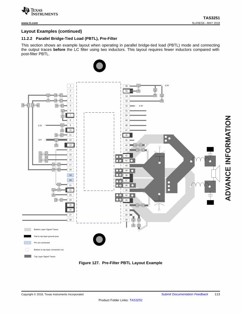
AD
VA
NC
E I
NF
OR
MA
TIO
N
0
0
27
28
26
23
24
21
22
19
20
17
18
15
16
13
7
32
31
34
33
36
38
37
40
39
42
41
44
43
46
45
48
47
9
10
8
35
29
14
49
50
25
12
11
52
51
55
56
5
6
3
4
2
1
3.3V
12V
30
3.3V
54
53
3.3V
Pin not connected
Bottom to top layer connection via
Top Layer Signal Traces
Pad to top layer ground pour
Bottom Layer Signal Traces
113
TAS3251www.ti.com SLASEG6 –MAY 2018
Product Folder Links: TAS3251
Submit Documentation FeedbackCopyright © 2018, Texas Instruments Incorporated
Layout Examples (continued)11.2.2 Parallel Bridge-Tied Load (PBTL), Pre-FilterThis section shows an example layout when operating in parallel bridge-tied load (PBTL) mode and connectingthe output traces before the LC filter using two inductors. This layout requires fewer inductors compared withpost-filter PBTL.
Figure 127. Pre-Filter PBTL Layout Example

AD
VA
NC
E IN
FO
RM
AT
ION
0
0
27
28
26
23
24
21
22
19
20
17
18
15
16
13
7
32
31
34
33
36
38
37
40
39
42
41
44
43
46
45
48
47
9
10
8
35
29
14
49
50
25
12
11
52
51
55
56
5
6
3
4
2
1
3.3V
12V
30
3.3V
54
53
3.3V
Pin not connected
Bottom to top layer connection via
Top layer signal traces
Pad to top layer ground pour
Bottom layer signal traces
114
TAS3251SLASEG6 –MAY 2018 www.ti.com
Product Folder Links: TAS3251
Submit Documentation Feedback Copyright © 2018, Texas Instruments Incorporated
Layout Examples (continued)11.2.3 Parallel Bridge-Tied Load (PBTL), Post-FilterThis section shows an example layout when operating in parallel bridge-tied load (PBTL) mode and connectingthe output traces after the LC filter using four inductors. This layout requires fewer inductors compared with post-filter PBTL.
Figure 128. Post-Filter PBTL Layout Example

AD
VA
NC
E I
NF
OR
MA
TIO
N
115
TAS3251www.ti.com SLASEG6 –MAY 2018
Product Folder Links: TAS3251
Submit Documentation FeedbackCopyright © 2018, Texas Instruments Incorporated
12 Device and Documentation Support
12.1 Device Support
12.1.1 Device NomenclatureThe glossary listed in the Glossary section is a general glossary with commonly used acronyms and words whichare defined in accordance with a broad TI initiative to comply with industry standards such as JEDEC, IPC, IEEE,and others. The glossary provided in this section defines words, phrases, and acronyms that are unique to thisproduct and documentation, collateral, or support tools and software used with this product. For any additionalquestions regarding definitions and terminology, please see the e2e Audio Amplfier Forum.
Bridge tied load (BTL) is an output configuration in which one terminal of the speaker is connected to one half-bridge and the other terminal is connected to another half-bridge.
DUT refers to a device under test to differentiate one device from another.
Closed-loop architecture describes a topology in which the amplifier monitors the output terminals, comparingthe output signal to the input signal and attempts to correct for non-linearities in the output.
Dynamic controls are those which are changed during normal use by either the system or the end-user.
GPIO is a general purpose input/output pin. It is a highly configurable, bi-directional digital pin which can performmany functions as required by the system.
Host processor (also known as System Processor, Scalar, Host, or System Controller) refers to devicewhich serves as a central system controller, providing control information to devices connected to it as well asgathering audio source data from devices upstream from it and distributing it to other devices. This device oftenconfigures the controls of the audio processing devices (like the TAS3251) in the audio path in order to optimizethe audio output of a loudspeaker based on frequency response, time alignment, target sound pressure level,safe operating area of the system, and user preference.
HybridFlow uses components which are built in RAM and components which are built in ROM to make aconfigurable device that is easier to use than a fully-programmable device while remaining flexible enough to beused in several applications
Maximum continuous output power refers to the maximum output power that the amplifier can continuouslydeliver without shutting down when operated in a 25°C ambient temperature. Testing is performed for the periodof time required that their temperatures reach thermal equilibrium and are no longer increasing
Parallel bridge tied load (PBTL) is an output configuration in which one terminal of the speaker is connected totwo half-bridges which have been placed in parallel and the other terminal is connected to another pair of halfbridges placed in parallel
rDS(on) is a measure of the on-resistance of the MOSFETs used in the output stage of the amplifier.
Static controls/Static configurations are controls which do not change while the system is in normal use.
Vias are copper-plated through-hole in a PCB.
12.1.2 Development Support• TAS3251 Evaluation Module (TAS3251EVM)• PurePath™ Console 3 Software (PUREPATHCONSOLE)• Speaker Characterization Board for PurePath™ Audio SmartAmp (PP-SALB-EVM)

AD
VA
NC
E IN
FO
RM
AT
ION
116
TAS3251SLASEG6 –MAY 2018 www.ti.com
Product Folder Links: TAS3251
Submit Documentation Feedback Copyright © 2018, Texas Instruments Incorporated
12.2 Community ResourcesThe following links connect to TI community resources. Linked contents are provided "AS IS" by the respectivecontributors. They do not constitute TI specifications and do not necessarily reflect TI's views; see TI's Terms ofUse.
TI E2E™ Online Community TI's Engineer-to-Engineer (E2E) Community. Created to foster collaborationamong engineers. At e2e.ti.com, you can ask questions, share knowledge, explore ideas and helpsolve problems with fellow engineers.
Design Support TI's Design Support Quickly find helpful E2E forums along with design support tools andcontact information for technical support.
12.3 TrademarksBurr-Brown, PurePath, PowerPAD, E2E are trademarks of Texas Instruments.All other trademarks are the property of their respective owners.
12.4 Electrostatic Discharge CautionThese devices have limited built-in ESD protection. The leads should be shorted together or the device placed in conductive foamduring storage or handling to prevent electrostatic damage to the MOS gates.
12.5 GlossarySLYZ022 — TI Glossary.
This glossary lists and explains terms, acronyms, and definitions.
13 Mechanical, Packaging, and Orderable InformationThe following pages include mechanical, packaging, and orderable information. This information is the mostcurrent data available for the designated devices. This data is subject to change without notice and revision ofthis document. For browser-based versions of this data sheet, refer to the left-hand navigation.

PACKAGE OPTION ADDENDUM
www.ti.com 30-Aug-2018
Addendum-Page 1
PACKAGING INFORMATION
Orderable Device Status(1)
Package Type PackageDrawing
Pins PackageQty
Eco Plan(2)
Lead/Ball Finish(6)
MSL Peak Temp(3)
Op Temp (°C) Device Marking(4/5)
Samples
TAS3251DKQ ACTIVE HSSOP DKQ 56 20 Green (RoHS& no Sb/Br)
CU NIPDAU Level-3-260C-168 HR 0 to 70 3251
TAS3251DKQR ACTIVE HSSOP DKQ 56 1000 Green (RoHS& no Sb/Br)
CU NIPDAU Level-3-260C-168 HR 0 to 70 3251
(1) The marketing status values are defined as follows:ACTIVE: Product device recommended for new designs.LIFEBUY: TI has announced that the device will be discontinued, and a lifetime-buy period is in effect.NRND: Not recommended for new designs. Device is in production to support existing customers, but TI does not recommend using this part in a new design.PREVIEW: Device has been announced but is not in production. Samples may or may not be available.OBSOLETE: TI has discontinued the production of the device.
(2) RoHS: TI defines "RoHS" to mean semiconductor products that are compliant with the current EU RoHS requirements for all 10 RoHS substances, including the requirement that RoHS substancedo not exceed 0.1% by weight in homogeneous materials. Where designed to be soldered at high temperatures, "RoHS" products are suitable for use in specified lead-free processes. TI mayreference these types of products as "Pb-Free".RoHS Exempt: TI defines "RoHS Exempt" to mean products that contain lead but are compliant with EU RoHS pursuant to a specific EU RoHS exemption.Green: TI defines "Green" to mean the content of Chlorine (Cl) and Bromine (Br) based flame retardants meet JS709B low halogen requirements of <=1000ppm threshold. Antimony trioxide basedflame retardants must also meet the <=1000ppm threshold requirement.
(3) MSL, Peak Temp. - The Moisture Sensitivity Level rating according to the JEDEC industry standard classifications, and peak solder temperature.
(4) There may be additional marking, which relates to the logo, the lot trace code information, or the environmental category on the device.
(5) Multiple Device Markings will be inside parentheses. Only one Device Marking contained in parentheses and separated by a "~" will appear on a device. If a line is indented then it is a continuationof the previous line and the two combined represent the entire Device Marking for that device.
(6) Lead/Ball Finish - Orderable Devices may have multiple material finish options. Finish options are separated by a vertical ruled line. Lead/Ball Finish values may wrap to two lines if the finishvalue exceeds the maximum column width.
Important Information and Disclaimer:The information provided on this page represents TI's knowledge and belief as of the date that it is provided. TI bases its knowledge and belief on informationprovided by third parties, and makes no representation or warranty as to the accuracy of such information. Efforts are underway to better integrate information from third parties. TI has taken andcontinues to take reasonable steps to provide representative and accurate information but may not have conducted destructive testing or chemical analysis on incoming materials and chemicals.TI and TI suppliers consider certain information to be proprietary, and thus CAS numbers and other limited information may not be available for release.
In no event shall TI's liability arising out of such information exceed the total purchase price of the TI part(s) at issue in this document sold by TI to Customer on an annual basis.

PACKAGE OPTION ADDENDUM
www.ti.com 30-Aug-2018
Addendum-Page 2


www.ti.com
PACKAGE OUTLINE
C
TYP10.6710.03
54X 0.635
56X 0.370.17
2X17.15
TYP0.250.13
0 - 80.080.00
(6.34)
(5.14)
NOTE 6
2.4752.240
(2.29)
2.29 0.05
(1.18)
(1.26)
0.25GAGE PLANE
1.020.51
A
NOTE 3
18.5418.29
BNOTE 4
7.597.39
(3.04)
(3.04)
(3)
(4.455)
(1.74)
2X(0.23)
(2.455)
PowerPAD SSOP - 2.475 mm max heightDKQ0056BPLASTIC SMALL OUTLINE
4223602/A 04/2017
NOTES: 1. All linear dimensions are in millimeters. Any dimensions in parenthesis are for reference only. Dimensioning and tolerancing per ASME Y14.5M. 2. This drawing is subject to change without notice. 3. This dimension does not include mold flash, protrusions, or gate burrs. Mold flash, protrusions, or gate burrs shall not exceed 0.15 mm per side. 4. This dimension does not include interlead flash. Interlead flash shall not exceed 0.25 mm per side.5. The exposed thermal pad is designed to be attached to an external heatsink.6. For clamped heatsink design, refer to overall package height above the seating plane as 2.325 +/- 0.075 and molded body thickness dimension.
PowerPAD is a trademark of Texas Instruments.
TM
1 56
0.13 C A B
2928
PIN 1 ID AREA
THERMAL PADEXPOSED
SEATING PLANE
0.1 C
SEE DETAIL A
DETAIL ATYPICAL
SCALE 1.000

www.ti.com
EXAMPLE BOARD LAYOUT
(9.5)
0.05 MAXAROUND
0.05 MINAROUND
56X (1.9)
56X (0.4)
54X (0.635)
(R0.05) TYP
PowerPAD SSOP - 2.475 mm max heightDKQ0056BPLASTIC SMALL OUTLINE
4223602/A 04/2017
SYMM
SYMM
SEE DETAILS
LAND PATTERN EXAMPLEEXPOSED METAL SHOWN
SCALE:6X
1
28 29
56
NOTES: (continued) 7. Publication IPC-7351 may have alternate designs. 8. Solder mask tolerances between and around signal pads can vary based on board fabrication site. 9. Size of metal pad may vary due to creepage requirement.
TM
METALSOLDER MASKOPENING
NON SOLDER MASKDEFINED
SOLDER MASK DETAILSNOT TO SCALE
EXPOSED METAL
OPENINGSOLDER MASK METAL UNDER
SOLDER MASK
SOLDER MASKDEFINED
EXPOSED METAL

www.ti.com
EXAMPLE STENCIL DESIGN
56X (1.9)
56X (0.4)
54X (0.635)
(9.5)(R0.05) TYP
PowerPAD SSOP - 2.475 mm max heightDKQ0056BPLASTIC SMALL OUTLINE
4223602/A 04/2017
NOTES: (continued) 10. Laser cutting apertures with trapezoidal walls and rounded corners may offer better paste release. IPC-7525 may have alternate design recommendations. 11. Board assembly site may have different recommendations for stencil design.
SYMM
SYMM
1
28 29
56
TM
SOLDER PASTE EXAMPLEBASED ON 0.125 MM THICK STENCIL
SCALE:6X

IMPORTANT NOTICE
Texas Instruments Incorporated (TI) reserves the right to make corrections, enhancements, improvements and other changes to itssemiconductor products and services per JESD46, latest issue, and to discontinue any product or service per JESD48, latest issue. Buyersshould obtain the latest relevant information before placing orders and should verify that such information is current and complete.TI’s published terms of sale for semiconductor products (http://www.ti.com/sc/docs/stdterms.htm) apply to the sale of packaged integratedcircuit products that TI has qualified and released to market. Additional terms may apply to the use or sale of other types of TI products andservices.Reproduction of significant portions of TI information in TI data sheets is permissible only if reproduction is without alteration and isaccompanied by all associated warranties, conditions, limitations, and notices. TI is not responsible or liable for such reproduceddocumentation. Information of third parties may be subject to additional restrictions. Resale of TI products or services with statementsdifferent from or beyond the parameters stated by TI for that product or service voids all express and any implied warranties for theassociated TI product or service and is an unfair and deceptive business practice. TI is not responsible or liable for any such statements.Buyers and others who are developing systems that incorporate TI products (collectively, “Designers”) understand and agree that Designersremain responsible for using their independent analysis, evaluation and judgment in designing their applications and that Designers havefull and exclusive responsibility to assure the safety of Designers' applications and compliance of their applications (and of all TI productsused in or for Designers’ applications) with all applicable regulations, laws and other applicable requirements. Designer represents that, withrespect to their applications, Designer has all the necessary expertise to create and implement safeguards that (1) anticipate dangerousconsequences of failures, (2) monitor failures and their consequences, and (3) lessen the likelihood of failures that might cause harm andtake appropriate actions. Designer agrees that prior to using or distributing any applications that include TI products, Designer willthoroughly test such applications and the functionality of such TI products as used in such applications.TI’s provision of technical, application or other design advice, quality characterization, reliability data or other services or information,including, but not limited to, reference designs and materials relating to evaluation modules, (collectively, “TI Resources”) are intended toassist designers who are developing applications that incorporate TI products; by downloading, accessing or using TI Resources in anyway, Designer (individually or, if Designer is acting on behalf of a company, Designer’s company) agrees to use any particular TI Resourcesolely for this purpose and subject to the terms of this Notice.TI’s provision of TI Resources does not expand or otherwise alter TI’s applicable published warranties or warranty disclaimers for TIproducts, and no additional obligations or liabilities arise from TI providing such TI Resources. TI reserves the right to make corrections,enhancements, improvements and other changes to its TI Resources. TI has not conducted any testing other than that specificallydescribed in the published documentation for a particular TI Resource.Designer is authorized to use, copy and modify any individual TI Resource only in connection with the development of applications thatinclude the TI product(s) identified in such TI Resource. NO OTHER LICENSE, EXPRESS OR IMPLIED, BY ESTOPPEL OR OTHERWISETO ANY OTHER TI INTELLECTUAL PROPERTY RIGHT, AND NO LICENSE TO ANY TECHNOLOGY OR INTELLECTUAL PROPERTYRIGHT OF TI OR ANY THIRD PARTY IS GRANTED HEREIN, including but not limited to any patent right, copyright, mask work right, orother intellectual property right relating to any combination, machine, or process in which TI products or services are used. Informationregarding or referencing third-party products or services does not constitute a license to use such products or services, or a warranty orendorsement thereof. Use of TI Resources may require a license from a third party under the patents or other intellectual property of thethird party, or a license from TI under the patents or other intellectual property of TI.TI RESOURCES ARE PROVIDED “AS IS” AND WITH ALL FAULTS. TI DISCLAIMS ALL OTHER WARRANTIES ORREPRESENTATIONS, EXPRESS OR IMPLIED, REGARDING RESOURCES OR USE THEREOF, INCLUDING BUT NOT LIMITED TOACCURACY OR COMPLETENESS, TITLE, ANY EPIDEMIC FAILURE WARRANTY AND ANY IMPLIED WARRANTIES OFMERCHANTABILITY, FITNESS FOR A PARTICULAR PURPOSE, AND NON-INFRINGEMENT OF ANY THIRD PARTY INTELLECTUALPROPERTY RIGHTS. TI SHALL NOT BE LIABLE FOR AND SHALL NOT DEFEND OR INDEMNIFY DESIGNER AGAINST ANY CLAIM,INCLUDING BUT NOT LIMITED TO ANY INFRINGEMENT CLAIM THAT RELATES TO OR IS BASED ON ANY COMBINATION OFPRODUCTS EVEN IF DESCRIBED IN TI RESOURCES OR OTHERWISE. IN NO EVENT SHALL TI BE LIABLE FOR ANY ACTUAL,DIRECT, SPECIAL, COLLATERAL, INDIRECT, PUNITIVE, INCIDENTAL, CONSEQUENTIAL OR EXEMPLARY DAMAGES INCONNECTION WITH OR ARISING OUT OF TI RESOURCES OR USE THEREOF, AND REGARDLESS OF WHETHER TI HAS BEENADVISED OF THE POSSIBILITY OF SUCH DAMAGES.Unless TI has explicitly designated an individual product as meeting the requirements of a particular industry standard (e.g., ISO/TS 16949and ISO 26262), TI is not responsible for any failure to meet such industry standard requirements.Where TI specifically promotes products as facilitating functional safety or as compliant with industry functional safety standards, suchproducts are intended to help enable customers to design and create their own applications that meet applicable functional safety standardsand requirements. Using products in an application does not by itself establish any safety features in the application. Designers mustensure compliance with safety-related requirements and standards applicable to their applications. Designer may not use any TI products inlife-critical medical equipment unless authorized officers of the parties have executed a special contract specifically governing such use.Life-critical medical equipment is medical equipment where failure of such equipment would cause serious bodily injury or death (e.g., lifesupport, pacemakers, defibrillators, heart pumps, neurostimulators, and implantables). Such equipment includes, without limitation, allmedical devices identified by the U.S. Food and Drug Administration as Class III devices and equivalent classifications outside the U.S.TI may expressly designate certain products as completing a particular qualification (e.g., Q100, Military Grade, or Enhanced Product).Designers agree that it has the necessary expertise to select the product with the appropriate qualification designation for their applicationsand that proper product selection is at Designers’ own risk. Designers are solely responsible for compliance with all legal and regulatoryrequirements in connection with such selection.Designer will fully indemnify TI and its representatives against any damages, costs, losses, and/or liabilities arising out of Designer’s non-compliance with the terms and provisions of this Notice.
Mailing Address: Texas Instruments, Post Office Box 655303, Dallas, Texas 75265Copyright © 2018, Texas Instruments Incorporated