Embed Size (px)
Citation preview

19-4349; Rev 2; 2/12
For pricing, delivery, and ordering information, please contact Maxim Directat 1-888-629-4642, or visit Maxim’s website at www.maximintegrated.com.
MAX986016-Bit Mono Audio Voice Codec
General DescriptionThe MAX9860 is a low-power, voiceband, mono audiocodec designed to provide a complete audio solutionfor wireless voice headsets and other mono voice audiodevices. Using an on-chip bridge-tied load mono head-phone amplifier, the MAX9860 can output 30mW into a32Ω earpiece while operating from a single 1.8V powersupply. Very low power consumption makes it an idealchoice for battery-powered applications.
The MAX9860’s flexible clocking circuitry utilizes com-mon system clock frequencies ranging from 10MHz to60MHz, eliminating the need for an external PLL andmultiple crystal oscillators. Both the ADC and DAC sup-port sample rates of 8kHz to 48kHz in either synchro-nous or asynchronous operation. Both master and slavetiming modes are supported.
Two differential microphone inputs are available with auser-programmable preamplifier and programmablegain amplifier. Automatic gain control with selectableattack/release times and signal threshold allows maxi-mum dynamic range. A noise gate with selectablethreshold provides a means to quiet the channel whenno signal is present. Both the DAC and ADC digital filtersprovide full attenuation for out-of-band signals as well asa 5th order GSM-compliant digital highpass filter. A digi-tal side tone mixer provides loopback of the micro-phones/ADC signal to the DAC/headphone output.
Serial DAC and ADC data is transferred over a flexibledigital I2S-compatible interface that also supports TDMmode. Mode settings, volume control, and shutdown areprogrammed through a 2-wire, I2C-compatible interface.
The MAX9860 is fully specified over the -40°C to +85°Cextended temperature range and is available in a low-profile, 4mm x 4mm, 24-pin thin QFN package.
ApplicationsAudio Headsets
Portable Navigation Device
Mobile Phones
Smart Phones
VoIP Phones
Audio Accessories
Features 1.8V Single-Supply Operation
Digital Highpass Elliptical Filters with Notch for217Hz (GSM)
Mono 30mW BTL Headphone Amplifier
Dual Low-Noise Microphone Inputs
Automatic Microphone Gain Control and NoiseGate
90dB DAC DR (fS = 48kHz)
81dB ADC DR (fS = 48kHz)
Supports Master Clock Frequencies from 10MHzto 60MHz
Supports Sample Rates from 8kHz to 48kHz
Flexible Digital Audio Interface
Clickless/Popless Operation
2-Wire, I2C-Compatible Control Interface
Available in 24-Pin, Thin QFN, 4mm x 4mm x0.8mm Package
Ordering InformationPART TEMP RANGE PIN-PACKAGE
MAX9860ETG+ -40°C to +85°C 24 TQFN-EP*
+Denotes a lead-free/RoHS-compliant package.
*EP = Exposed pad.
ADC
ADC
DIGITALAUDIO
INTERFACE
DIGITALFILTERING
ANDMIXERS
DIFFMIC
DIFFMIC
DAC
AVDD AND DVDD1.7V TO 1.9V
DVDDIO1.7V TO 3.6V
CLOCKCONTROL
DIGITAL AUDIOINPUT/OUTPUT
I2CINTERFACE
MAX9860
Simplified Block Diagram
Pin Configuration and Typical Operating Circuit appear atend of data sheet.
MAX986016-Bit Mono Audio Voice Codec
2 Maxim Integrated
ABSOLUTE MAXIMUM RATINGS
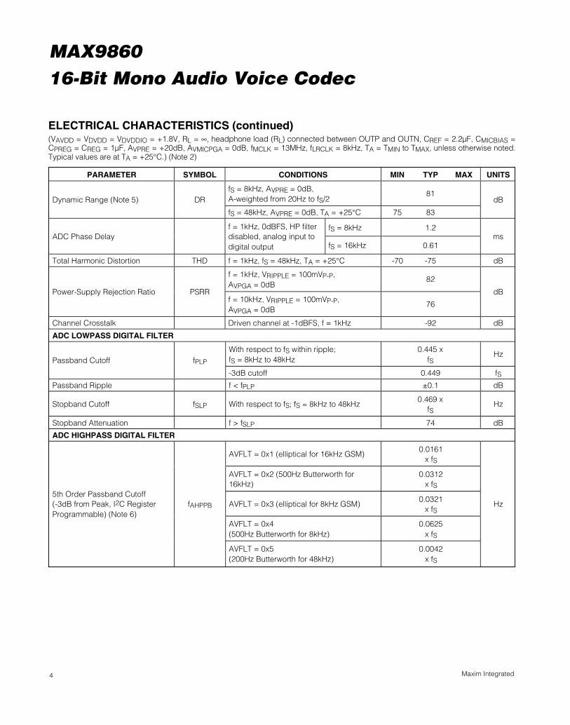
ELECTRICAL CHARACTERISTICS(VAVDD = VDVDD = VDVDDIO = +1.8V, RL = ∞, headphone load (RL) connected between OUTP and OUTN, CREF = 2.2µF, CMICBIAS =CPREG = CREG = 1µF, AVPRE = +20dB, AVMICPGA = 0dB, fMCLK = 13MHz, fLRCLK = 8kHz, TA = TMIN to TMAX, unless otherwise noted.Typical values are at TA = +25°C.) (Note 2)
Stresses beyond those listed under “Absolute Maximum Ratings” may cause permanent damage to the device. These are stress ratings only, and functionaloperation of the device at these or any other conditions beyond those indicated in the operational sections of the specifications is not implied. Exposure toabsolute maximum rating conditions for extended periods may affect device reliability.
(Voltages referenced to AGND.)DVDDIO, SDA, SCL, IRQ.......................................-0.3V to +3.6VAVDD, DVDD............................................................-0.3V to +2VAGND, DGND, MICGND.......................................-0.3V to +0.3VOUTP, OUTN, PREG, REF, MICBIAS .....-0.3V to (VAVDD + 0.3V)MICLP, MICLN, MICRP, MICRN, REG....-0.3V to (VPREG + 0.3V)MCLK, LRCLK, BCLK,
SDOUT, SDIN..................................-0.3V to (VDVDDIO + 0.3V)
Continuous Power Dissipation (TA = +70°C)24-Pin TQFN (derate 27.8mW/°C above +70°C,
multilayer board) ......................................................2222mWOperating Temperature Range ...........................-40°C to +85°CStorage Temperature Range .............................-65°C to +150°CJunction Temperature ......................................................+150°CLead Temperature (soldering, 10s) .................................+300°CSoldering Temperature (reflow) .......................................+260°C
PARAMETER SYMBOL CONDITIONS MIN TYP MAX UNITS
AVDD (inferred from HP output PSRR) 1.7 1.8 1.9
DVDD (inferred from codec performancetests)
1.7 1.8 1.9Supply Voltage Range
DVDDIO 1.7 1.8 3.6
V
AVDD 1.46 2.2DAC playback mode(48kHz) DVDD 1.05 1.6
AVDD 4.08 5.7Full operation8kHz mono ADC + DAC DVDD 0.78 1.0
AVDD 6.17 9.0Full operation8kHz stereo ADC + DAC DVDD 0.8 1.2
AVDD 5.38 8.0
Total Supply Current(Note 3)
IAVDD+DVDD
Stereo ADC only (48kHz)DVDD 1.68 2.2
mA
AVDD 0.56 5Shutdown Supply Current ISHDN TA = +25°C DVDD +
DVDDIO1.65 5
µA
Shutdown to Full Operation 10 msDAC (Note 4)Gain Error ±1 ±5 %
Dynamic Range (Note 5) DR+ 0d B vol um e setti ng , fS = 8kH z, m easur ed at headphone output, TA = +25°C
84 90 dB
DAC Full-Scale Output 1 VRMS
fS = 8kHz 1.2DAC Path Phase Delay
f = 1kHz, 0dBFS, HPfilter disabled, digitalinput to analog output fS = 16kHz 0.59
ms
Total Harmonic Distortion + Noise THD+Nf = 1kHz, fMCLK = 12.288MHz,fLRCLK = 48kHz
-87 dB
Note 1: Package thermal resistances were obtained using the method described in JEDEC specification JESD51-7, using a four-layerboard. For detailed information on package thermal considerations, refer to www.maximintegrated.com/thermal-tutorial.
PACKAGE THERMAL CHARACTERISTICS (Note 1)TQFN
Junction-to-Ambient Thermal Resistance (θJA)...............36°C/WJunction-to-Case Thermal Resistance (θJC)......................3°C/W
MAX986016-Bit Mono Audio Voice Codec
3Maxim Integrated
PARAMETER SYMBOL CONDITIONS MIN TYP MAX UNITS
f = 1kHz, VRIPPLE = 100mVP-P,AVPGA = 0dB
94
Power-Supply Rejection Ratio PSRRf = 10kHz, VRIPPLE = 100mVP-P,AVPGA = 0dB
71
dB
DAC LOWPASS DIGITAL FILTER
With respect to fS within ripple; fS = 8kHzto 48kHz
0.448 xfS
HzPassband Cutoff fPLP
-3dB cutoff 0.451 fSPassband Ripple f < fPLP ±0.1 dB
Stopband Cutoff fSLP With respect to fS; fS = 8kHz to 48kHz0.476 x
fSHz
Stopband Attenuation f > fSLP, f = 20Hz to 20kHz 75 dB
DAC HIGHPASS DIGITAL FILTER
DVFLT = 0x1(elliptical for 16kHz GSM)
0.0161x fS
DVFLT = 0x2(500Hz Butterworth for 16kHz)
0.0312x fS
DVFLT = 0x3(elliptical for 8kHz GSM)
0.0321x fS
DVFLT = 0x4(500Hz Butterworth for 8kHz)
0.0625x fS
5th Order Passband Cutoff(-3dB from Peak, I2C RegisterProgrammable) (Note 6)
fDHPPB
DVFLT = 0x5(200Hz Butterworth for 48kHz)
0.0042x fS
Hz
DVFLT = 0x1(elliptical for 16kHz GSM)
0.0139x fS
DVFLT = 0x2(500Hz Butterworth for 16kHz)
0.0156x fS
DVFLT = 0x3(elliptical for 8kHz GSM)
0.0279x fS
DVFLT = 0x4(500Hz Butterworth for 8kHz)
0.0312x fS
5th Order Stopband Cutoff(-30dB from Peak, I2C RegisterProgrammable) (Note 6)
fDHPSB
DVFLT = 0x5(200Hz Butterworth for 48kHz)
0.0021x fS
Hz
DC Blocking DCAtten DVFLT ≠ 0x0 90 dB
ADC
Full-Scale Input Voltage 0dBFSDifferential MIC Input, AVPRE = 0dB,AVPGA = 0dB
1 VP-P
Channel Gain Mismatch ±0.3 %
ELECTRICAL CHARACTERISTICS (continued)(VAVDD = VDVDD = VDVDDIO = +1.8V, RL = ∞, headphone load (RL) connected between OUTP and OUTN, CREF = 2.2µF, CMICBIAS =CPREG = CREG = 1µF, AVPRE = +20dB, AVMICPGA = 0dB, fMCLK = 13MHz, fLRCLK = 8kHz, TA = TMIN to TMAX, unless otherwise noted.Typical values are at TA = +25°C.) (Note 2)
MAX986016-Bit Mono Audio Voice Codec
4 Maxim Integrated
ELECTRICAL CHARACTERISTICS (continued)(VAVDD = VDVDD = VDVDDIO = +1.8V, RL = ∞, headphone load (RL) connected between OUTP and OUTN, CREF = 2.2µF, CMICBIAS =CPREG = CREG = 1µF, AVPRE = +20dB, AVMICPGA = 0dB, fMCLK = 13MHz, fLRCLK = 8kHz, TA = TMIN to TMAX, unless otherwise noted.Typical values are at TA = +25°C.) (Note 2)
PARAMETER SYMBOL CONDITIONS MIN TYP MAX UNITS
fS = 8kHz, AVPRE = 0dB,A-weighted from 20Hz to fS/2
81Dynamic Range (Note 5) DR
fS = 48kHz, AVPRE = 0dB, TA = +25°C 75 83
dB
fS = 8kHz 1.2ADC Phase Delay
f = 1kHz, 0dBFS, HP filterdisabled, analog input todigital output fS = 16kHz 0.61
ms
Total Harmonic Distortion THD f = 1kHz, fS = 48kHz, TA = +25°C -70 -75 dB
f = 1kHz, VRIPPLE = 100mVP-P,AVPGA = 0dB
82
Power-Supply Rejection Ratio PSRRf = 10kHz, VRIPPLE = 100mVP-P,AVPGA = 0dB
76
dB
Channel Crosstalk Driven channel at -1dBFS, f = 1kHz -92 dB
ADC LOWPASS DIGITAL FILTER
With respect to fS within ripple;fS = 8kHz to 48kHz
0.445 xfS
HzPassband Cutoff fPLP
-3dB cutoff 0.449 fSPassband Ripple f < fPLP ±0.1 dB
Stopband Cutoff fSLP With respect to fS; fS = 8kHz to 48kHz0.469 x
fSHz
Stopband Attenuation f > fSLP 74 dB
ADC HIGHPASS DIGITAL FILTER
AVFLT = 0x1 (elliptical for 16kHz GSM)0.0161
x fS
AVFLT = 0x2 (500Hz Butterworth for16kHz)
0.0312x fS
AVFLT = 0x3 (elliptical for 8kHz GSM)0.0321
x fS
AVFLT = 0x4(500Hz Butterworth for 8kHz)
0.0625x fS
5th Order Passband Cutoff(-3dB from Peak, I2C RegisterProgrammable) (Note 6)
fAHPPB
AVFLT = 0x5(200Hz Butterworth for 48kHz)
0.0042x fS
Hz

MAX986016-Bit Mono Audio Voice Codec
5Maxim Integrated
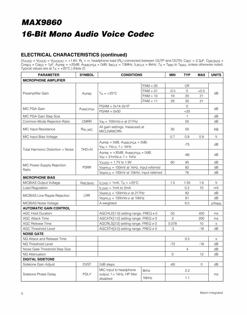
ELECTRICAL CHARACTERISTICS (continued)(VAVDD = VDVDD = VDVDDIO = +1.8V, RL = ∞, headphone load (RL) connected between OUTP and OUTN, CREF = 2.2µF, CMICBIAS =CPREG = CREG = 1µF, AVPRE = +20dB, AVMICPGA = 0dB, fMCLK = 13MHz, fLRCLK = 8kHz, TA = TMIN to TMAX, unless otherwise noted.Typical values are at TA = +25°C.) (Note 2)
PARAMETER SYMBOL CONDITIONS MIN TYP MAX UNITS
AVFLT = 0x1(elliptical for 16kHz GSM)
0.0139x fS
AVFLT = 0x2(500Hz Butterworth for 16kHz)
0.0156x fS
AVFLT = 0x3(elliptical for 8kHz GSM)
0.0279x fS
AVFLT = 0x4(500Hz Butterworth for 8kHz)
0.0312x fS
5th Order Stopband Cutoff(-30dB from peak, I2C RegisterProgrammable) (Note 6)
fAHPSB
AVFLT = 0x5(200Hz Butterworth for 48kHz)
0.0021x fS
Hz
DC Blocking DCATTEN AVFLT ≠ 0x0 90 dBCLOCKING
MCLK Input FrequencyMCLK is not required to be synchronousor related to the desired LRCLK data rate
10 60 MHz
MCLK Duty Cycle 40 50 60 %
Maximum MCLK Input Jitter For guaranteed performance limits 100 psRMS
LRCLK Data Rate Frequency 8 48 kHz
LRCLK PLL Lock Time 12 25 ms
LRCLK Acceptable Jitter forMaintaining PLL Lock
±20 ns
MONO HEADPHONE AMPLIFIERRL = 16Ω 30 50
Output Power POUTf = 1kHz, THD+N ≤ 1%TA = +25°C RL = 32Ω 33
mW
RL = 32Ω, POUT = 25mW, f = 1kHz 0.05Total Harmonic Distortion + Noise THD+N
RL = 16Ω, POUT = 25mW, f = 1kHz 0.08%
Dynamic Range (Note 5) DR+0dB volume setting, DAC input atfS = 8kHz to 48kHz
90 dB
VAVDD = 1.7V to 1.9V 60 84
VRIPPLE = 100mVP-P, f = 217Hz 86Power-Supply Rejection Ratio PSRR
VRIPPLE = 100mVP-P, f = 20kHz 71
dB
Output Offset Voltage VOS VOUTP - VOUTN, TA =+25°C ± 3.5 mV
RL = 32Ω 500Capacitive Drive Capability No sustained oscillations
RL = ∞ 100pF
Click-and-Pop LevelPeak voltage into/out of shutdown, 32sps,A-weighted
-70 dBV
MAX986016-Bit Mono Audio Voice Codec
6 Maxim Integrated
ELECTRICAL CHARACTERISTICS (continued)(VAVDD = VDVDD = VDVDDIO = +1.8V, RL = ∞, headphone load (RL) connected between OUTP and OUTN, CREF = 2.2µF, CMICBIAS =CPREG = CREG = 1µF, AVPRE = +20dB, AVMICPGA = 0dB, fMCLK = 13MHz, fLRCLK = 8kHz, TA = TMIN to TMAX, unless otherwise noted.Typical values are at TA = +25°C.) (Note 2)
PARAMETER SYMBOL CONDITIONS MIN TYP MAX UNITS
MICROPHONE AMPLIFIER
PAM = 00 Off
PAM = 01 -0.5 0 +0.5PAM = 10 19 20 21
Preamplifier Gain AVPRE TA = +25°C
PAM = 11 29 30 31
dB
PGAM = 0x14–0x1F 0MIC PGA Gain AVMICPGA
PGAM = 0x00 +20dB
MIC PGA Gain Step Size 1 dB
Common-Mode Rejection Ratio CMRR VIN = 100mVP-P at 217Hz 50 dB
MIC Input Resistance RIN_MICAll gain settings, measured atMICLN/MICRN
30 50 kΩ
MIC Input Bias Voltage 0.7 0.8 0.9 V
AVPRE = 0dB, AVMICPGA = 0dB,VIN = 1VP-P, f = 1kHz
-75 dBTotal Harmonic Distortion + Noise THD+N
AVPRE = +30dB, AVMICPGA = 0dB,VIN = 31mVP-P, f = 1kHz
-66 dB
VAVDD = 1.7V to 1.9V 60 95 dB
VRIPPLE = 100mV at 1kHz, input referred 82 dBMIC Power-Supply RejectionRatio
PSRR
VRIPPLE = 100mV at 10kHz, input referred 76 dBMICROPHONE BIAS
MICBIAS Output Voltage VMICBIAS ILOAD = 1mA, TA = +25°C 1.5 1.55 1.6 V
Load Regulation ILOAD = 1mA to 2mA 0.2 10 mV
VRIPPLE = 100mVP-P at 217Hz 82 dBMICBIAS Line Ripple Rejection LRR
VRIPPLE = 100mVP-P at 10kHz 81 dB
MICBIAS Noise Voltage A-weighted 9.5 µVRMS
AUTOMATIC GAIN CONTROL
AGC Hold Duration AGCHLD[1:0] setting range, FREQ ≠ 0 50 400 msAGC Attack Time AGCATK[1:0] setting range, FREQ ≠ 0 3 200 ms
AGC Release Time AGCRLS[2:0] setting range, FREQ ≠ 0 0.078 10 s
AGC Threshold Level AGCSTH[3:0] setting range, FREQ ≠ 0 -3 -18 dB
NOISE GATENG Attack and Release Time 0.5 s
NG Threshold Level -72 -16 dB
Noise Gate Threshold Step Size 4 dB
NG Attenuation 0 12 dBDIGITAL SIDETONE
Sidetone Gain Adjust DVST 2dB steps -60 0 dB
8kHz 2.2Sidetone Phase Delay PDLY
MIC input to headphoneoutput, f = 1kHz, HP filterdisabled 16kHz 1.1
ms
MAX986016-Bit Mono Audio Voice Codec
7Maxim Integrated
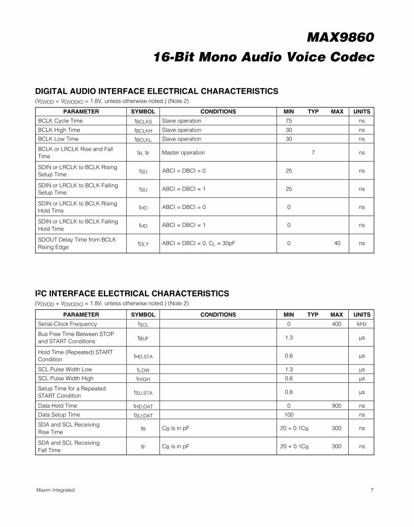
DIGITAL AUDIO INTERFACE ELECTRICAL CHARACTERISTICS(VDVDD = VDVDDIO = 1.8V, unless otherwise noted.) (Note 2)
PARAMETER SYMBOL CONDITIONS MIN TYP MAX UNITS
BCLK Cycle Time tBCLKS Slave operation 75 ns
BCLK High Time tBCLKH Slave operation 30 ns
BCLK Low Time tBCLKL Slave operation 30 ns
BCLK or LRCLK Rise and FallTime
tR, tF Master operation 7 ns
SDIN or LRCLK to BCLK RisingSetup Time
tSU ABCI = DBCI = 0 25 ns
SDIN or LRCLK to BCLK FallingSetup Time
tSU ABCI = DBCI = 1 25 ns
SDIN or LRCLK to BCLK RisingHold Time
tHD ABCI = DBCI = 0 0 ns
SDIN or LRCLK to BCLK FallingHold Time
tHD ABCI = DBCI = 1 0 ns
SDOUT Delay Time from BCLKRising Edge
tDLY ABCI = DBCI = 0, CL = 30pF 0 40 ns
I2C INTERFACE ELECTRICAL CHARACTERISTICS(VDVDD = VDVDDIO = 1.8V, unless otherwise noted.) (Note 2)
PARAMETER SYMBOL CONDITIONS MIN TYP MAX UNITS
Serial-Clock Frequency fSCL 0 400 kHz
Bus Free Time Between STOPand START Conditions
tBUF 1.3 µs
Hold Time (Repeated) STARTCondition
tHD,STA 0.6 µs
SCL Pulse Width Low tLOW 1.3 µs
SCL Pulse Width High tHIGH 0.6 µs
Setup Time for a RepeatedSTART Condition
tSU,STA 0.6 µs
Data Hold Time tHD,DAT 0 900 ns
Data Setup Time tSU,DAT 100 ns
SDA and SCL ReceivingRise Time
tR CB is in pF 20 + 0.1CB 300 ns
SDA and SCL ReceivingFall Time
tF CB is in pF 20 + 0.1CB 300 ns
MAX986016-Bit Mono Audio Voice Codec
8 Maxim Integrated
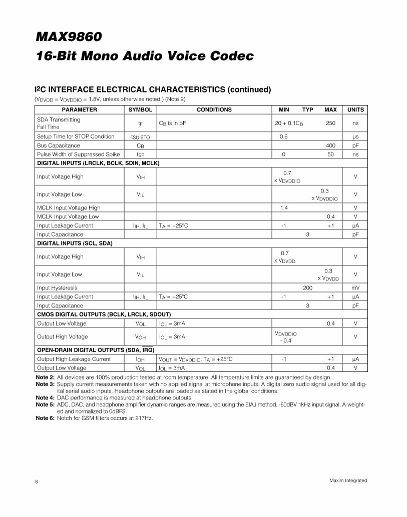
Note 2: All devices are 100% production tested at room temperature. All temperature limits are guaranteed by design.Note 3: Supply current measurements taken with no applied signal at microphone inputs. A digital zero audio signal used for all dig-
ital serial audio inputs. Headphone outputs are loaded as stated in the global conditions.Note 4: DAC performance is measured at headphone outputs.Note 5: ADC, DAC, and headphone amplifier dynamic ranges are measured using the EIAJ method. -60dBV 1kHz input signal, A-weight-
ed and normalized to 0dBFS.Note 6: Notch for GSM filters occurs at 217Hz.
PARAMETER SYMBOL CONDITIONS MIN TYP MAX UNITS
SDA TransmittingFall Time
tF CB is in pF 20 + 0.1CB 250 ns
Setup Time for STOP Condition tSU,STO 0.6 µs
Bus Capacitance CB 400 pF
Pulse Width of Suppressed Spike tSP 0 50 ns
DIGITAL INPUTS (LRCLK, BCLK, SDIN, MCLK)
Input Voltage High VIH0.7
x VDVDDIOV
Input Voltage Low VIL0.3
x VDVDDIOV
MCLK Input Voltage High 1.4 V
MCLK Input Voltage Low 0.4 V
Input Leakage Current IIH, IIL TA = +25°C -1 +1 µA
Input Capacitance 3 pF
DIGITAL INPUTS (SCL, SDA)
Input Voltage High VIH0.7
x VDVDDV
Input Voltage Low VIL0.3
x VDVDDV
Input Hysteresis 200 mV
Input Leakage Current IIH, IIL TA = +25oC -1 +1 µA
Input Capacitance 3 pF
CMOS DIGITAL OUTPUTS (BCLK, LRCLK, SDOUT)
Output Low Voltage VOL IOL = 3mA 0.4 V
Output High Voltage VOH IOL = 3mAVDVDDIO
- 0.4V
OPEN-DRAIN DIGITAL OUTPUTS (SDA, IRQ)
Output High Leakage Current IOH VOUT = VDVDDIO, TA = +25°C -1 +1 µA
Output Low Voltage VOL IOL = 3mA 0.4 V
I2C INTERFACE ELECTRICAL CHARACTERISTICS (continued)(VDVDD = VDVDDIO = 1.8V, unless otherwise noted.) (Note 2)

TOTAL HARMONIC DISTORTION + NOISEvs. OUTPUT POWER (DAC TO HP)
MAX
9860
toc0
1
OUTPUT POWER (mW)
THD+
N (%
)
252015105
0.01
0.1
1
10
0.0010 30
RL = 32Ω
f = 3.5kHz
f = 1kHz
f = 20kHz
TOTAL HARMONIC DISTORTION + NOISEvs. OUTPUT POWER (DAC TO HP)
MAX
9860
toc0
2
OUTPUT POWER (mW)
THD+
N (%
)
5040302010
0.01
0.1
1
10
0.0010 60
RL = 16Ω
f = 3.5kHz
f = 1kHz
f = 20kHz
TOTAL HARMONIC DISTORTION + NOISEvs. FREQUENCY (DAC TO HP)
MAX
9860
toc0
3
FREQUENCY (kHz)
THD+
N (%
)
10.1
0.01
0.1
1
10
0.0010.01 10
RL = 32Ω
POUT = 5mW
POUT = 20mW
TOTAL HARMONIC DISTORTION + NOISEvs. FREQUENCY (DAC TO HP)
MAX
9860
toc0
4
FREQUENCY (kHz)
THD+
N (%
)
10.1
0.01
0.1
1
10
0.0010.01 10
RL = 16Ω
POUT = 5mW
POUT = 20mW
TOTAL HARMONIC DISTORTION + NOISEvs. FREQUENCY (MICL TO ADC)
MAX
9860
toc0
5
FREQUENCY (kHz)
THD+
N (%
)
1010.1
0.01
0.1
1
10
0.0010.01 100
MICPRE = 0dBVIN = 1VP-P
TOTAL HARMONIC DISTORTION + NOISEvs. FREQUENCY (MICL TO ADC)
MAX
9860
toc0
6
FREQUENCY (kHz)
THD+
N (%
)
1010.1
0.1
1
10
0.010.01 100
MICPRE = +20dBVIN = 100mVP-P
TOTAL HARMONIC DISTORTION + NOISEvs. FREQUENCY (MICL TO ADC)
MAX
9860
toc0
7
FREQUENCY (kHz)
THD+
N (%
)
1010.1
0.01
0.1
1
10
0.0010.01 100
MICPRE = +30dBVIN = 31VP-P
HEADPHONE OUTPUT POWERvs. LOAD RESISTANCE
MAX
9860
toc0
8
LOAD RESISTANCE (Ω)
OUTP
UT P
OWER
(mW
)
125100755025
10
20
30
40
50
60
00 150
POWER-SUPPLY REJECTION RATIOvs. FREQUENCY (DAC TO HP)
MAX
9860
toc0
9
FREQUENCY (kHz)
PSRR
(dB)
1010.1
-110-100-90-80-70-60-50-40-30-20-10
0
-1200.01 100
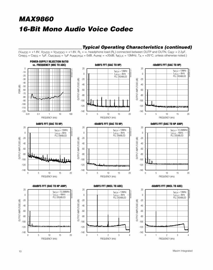
Typical Operating Characteristics(VAVDD = +1.8V, VDVDD = VDVDDIO = +1.8V, RL = ∞, headphone load (RL) connected between OUTP and OUTN, CREF = 2.2µF,CPREG = CREG = 1µF, CMICBIAS = 1µF AVMICPGA = 0dB, AVPRE = +20dB, fMCLK = 13MHz, TA = +25°C, unless otherwise noted.)
MAX986016-Bit Mono Audio Voice Codec
9Maxim Integrated
MAX986016-Bit Mono Audio Voice Codec
10 Maxim Integrated
POWER-SUPPLY REJECTION RATIOvs. FREQUENCY (MIC TO ADC)
MAX
9860
toc1
0
FREQUENCY (kHz)
PSRR
(dB)
1010.1
-110-100-90-80-70-60-50-40-30-20-10
0
-1200.01 100
0dBFS FFT (DAC TO HP)
MAX
9860
toc1
1
FREQUENCY (kHz)
OUTP
UT A
MPL
ITUD
E (d
B)
15105
-120
-100
-80
-60
-40
-20
0
20
-1400 20
fMCLK = 13MHzfLRCLK = 8kHzPLL DISABLED
-60dBFS FFT (DAC TO HP)
MAX
9860
toc1
2
FREQUENCY (kHz)
OUTP
UT A
MPL
ITUD
E (d
B)
15105
-120
-100
-80
-60
-40
-20
0
20
-1400 20
fMCLK = 13MHzfLRCLK = 8kHzPLL DISABLED
0dBFS FFT (DAC TO HP)
MAX
9860
toc1
3
FREQUENCY (kHz)
OUTP
UT A
MPL
ITUD
E (d
B)
15105
-120
-100
-80
-60
-40
-20
0
20
-1400 20
fMCLK = 13MHzfLRCLK = 8kHzPLL ENABLED
-60dBFS FFT (DAC TO HP)
MAX
9860
toc1
4
FREQUENCY (kHz)
OUTP
UT A
MPL
ITUD
E (d
B)
15105
-120
-100
-80
-60
-40
-20
0
20
-1400 20
fMCLK = 13MHzfLRCLK = 8kHzPLL ENABLED
0dBFS FFT (DAC TO HP AMP)
MAX
9860
toc1
5
FREQUENCY (kHz)
OUTP
UT A
MPL
ITUD
E (d
B)
15105
-120
-100
-80
-60
-40
-20
0
20
-1400 20
fMCLK = 12.288MHzfLRCLK = 48kHzPLL DISABLED
-60dBFS FFT (DAC TO HP AMP)
MAX
9860
toc1
6
FREQUENCY (kHz)
OUTP
UT A
MPL
ITUD
E (d
B)
15105
-120
-100
-80
-60
-40
-20
0
20
-1400 20
fMCLK = 12.288MHzfLRCLK = 48kHzPLL DISABLED
0dBFS FFT (MICL TO ADC)
MAX
9860
toc1
7
FREQUENCY (kHz)
OUTP
UT A
MPL
ITUD
E (d
B)
321
-120
-100
-80
-60
-40
-20
0
20
-1400 4
fMCLK = 13MHzfLRCLK = 8kHzPLL DISABLED
-60dBFS FFT (MICL TO ADC)M
AX98
60 to
c18
FREQUENCY (kHz)
OUTP
UT A
MPL
ITUD
E (d
B)
321
-120
-100
-80
-60
-40
-20
0
20
-1400 4
fMCLK = 13MHzfLRCLK = 8kHzPLL DISABLED
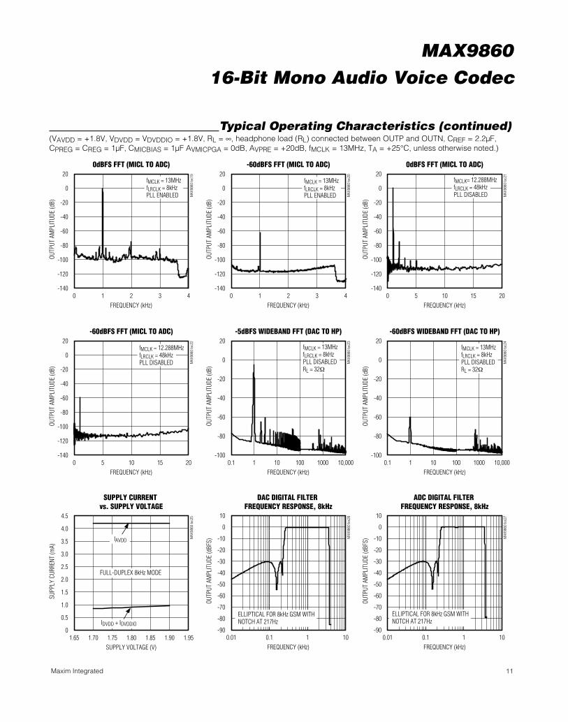
Typical Operating Characteristics (continued)(VAVDD = +1.8V, VDVDD = VDVDDIO = +1.8V, RL = ∞, headphone load (RL) connected between OUTP and OUTN, CREF = 2.2µF,CPREG = CREG = 1µF, CMICBIAS = 1µF AVMICPGA = 0dB, AVPRE = +20dB, fMCLK = 13MHz, TA = +25°C, unless otherwise noted.)
MAX986016-Bit Mono Audio Voice Codec
11Maxim Integrated
0dBFS FFT (MICL TO ADC)
MAX
9860
toc1
9
FREQUENCY (kHz)
OUTP
UT A
MPL
ITUD
E (d
B)
321
-120
-100
-80
-60
-40
-20
0
20
-1400 4
fMCLK = 13MHzfLRCLK = 8kHzPLL ENABLED
-60dBFS FFT (MICL TO ADC)
MAX
9860
toc2
0
FREQUENCY (kHz)
OUTP
UT A
MPL
ITUD
E (d
B)
321
-120
-100
-80
-60
-40
-20
0
20
-1400 4
fMCLK = 13MHzfLRCLK = 8kHzPLL ENABLED
0dBFS FFT (MICL TO ADC)
MAX
9860
toc2
1
FREQUENCY (kHz)
OUTP
UT A
MPL
ITUD
E (d
B)
15105
-120
-100
-80
-60
-40
-20
0
20
-1400 20
fMCLK= 12.288MHzfLRCLK = 48kHzPLL DISABLED
-60dBFS FFT (MICL TO ADC)
MAX
9860
toc2
2
FREQUENCY (kHz)
OUTP
UT A
MPL
ITUD
E (d
B)
15105
-120
-100
-80
-60
-40
-20
0
20
-1400 20
fMCLK = 12.288MHzfLRCLK = 48kHzPLL DISABLED
-5dBFS WIDEBAND FFT (DAC TO HP)
MAX
9860
toc2
3
FREQUENCY (kHz)
OUTP
UT A
MPL
ITUD
E (d
B)
1000100101
-80
-60
-40
-20
0
20
-1000.1 10,000
fMCLK = 13MHzfLRCLK = 8kHzPLL DISABLEDRL = 32Ω
-60dBFS WIDEBAND FFT (DAC TO HP)
MAX
9860
toc2
4
FREQUENCY (kHz)
OUTP
UT A
MPL
ITUD
E (d
B)
1000100101
-80
-60
-40
-20
0
20
-1000.1 10,000
fMCLK = 13MHzfLRCLK = 8kHzPLL DISABLEDRL = 32Ω
SUPPLY CURRENTvs. SUPPLY VOLTAGE
MAX
9860
toc2
5
SUPPLY VOLTAGE (V)
SUPP
LY C
URRE
NT (m
A)
1.901.851.801.751.70
0.5
1.0
1.5
2.0
2.5
3.0
3.5
4.0
4.5
01.65 1.95
IAVDD
IDVDD + IDVDDIO
FULL-DUPLEX 8kHz MODE
DAC DIGITAL FILTERFREQUENCY RESPONSE, 8kHz
MAX
9860
toc2
6
FREQUENCY (kHz)
OUTP
UT A
MPL
ITUD
E (d
BFS)
10.1
-80
-70
-60
-50
-40
-30
-20
-10
0
10
-900.01 10
ELLIPTICAL FOR 8kHz GSM WITHNOTCH AT 217Hz
ADC DIGITAL FILTERFREQUENCY RESPONSE, 8kHz
MAX
9860
toc2
7
FREQUENCY (kHz)
OUTP
UT A
MPL
ITUD
E (d
BFS)
10.1
-80
-70
-60
-50
-40
-30
-20
-10
0
10
-900.01 10
ELLIPTICAL FOR 8kHz GSM WITHNOTCH AT 217Hz
Typical Operating Characteristics (continued)(VAVDD = +1.8V, VDVDD = VDVDDIO = +1.8V, RL = ∞, headphone load (RL) connected between OUTP and OUTN, CREF = 2.2µF,CPREG = CREG = 1µF, CMICBIAS = 1µF AVMICPGA = 0dB, AVPRE = +20dB, fMCLK = 13MHz, TA = +25°C, unless otherwise noted.)
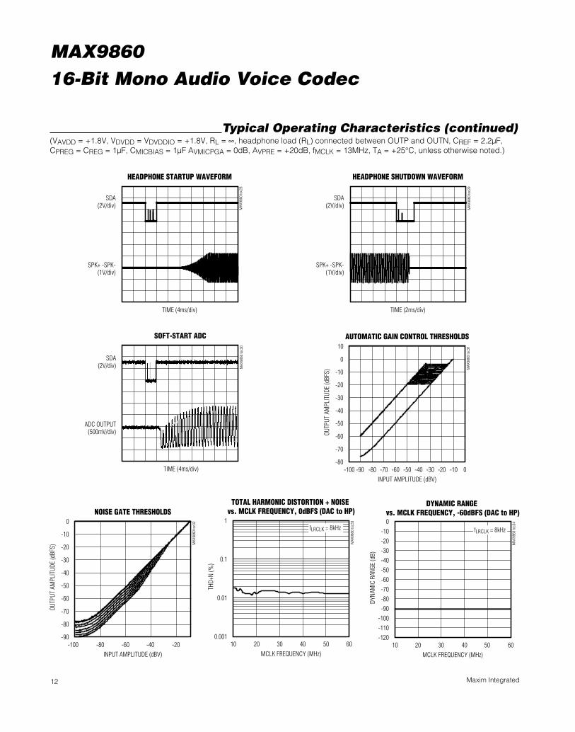
Typical Operating Characteristics (continued)(VAVDD = +1.8V, VDVDD = VDVDDIO = +1.8V, RL = ∞, headphone load (RL) connected between OUTP and OUTN, CREF = 2.2µF,CPREG = CREG = 1µF, CMICBIAS = 1µF AVMICPGA = 0dB, AVPRE = +20dB, fMCLK = 13MHz, TA = +25°C, unless otherwise noted.)
HEADPHONE STARTUP WAVEFORM
MAX
9860
toc2
8
TIME (4ms/div)
SPK+ -SPK-(1V/div)
SDA(2V/div)
HEADPHONE SHUTDOWN WAVEFORM
MAX
9860
toc2
9
TIME (2ms/div)
SPK+ -SPK-(1V/div)
SDA(2V/div)
ADC OUTPUT(500mV/div)
SDA(2V/div)
SOFT-START ADC
MAX
9860
toc3
0
TIME (4ms/div)-80
-60
-70
-40
-50
-30
-20
0
-10
10
-100 -80-90 -60-70 -40-50 -20-30 0-10
AUTOMATIC GAIN CONTROL THRESHOLDS
MAX
9860
toc3
1
INPUT AMPLITUDE (dBV)
OUTP
UT A
MPL
ITUD
E (d
BFS)
-90
-70
-80
-50
-60
-40
-30
-10
-20
0
-100 -80 -60 -40 -20
NOISE GATE THRESHOLDS
MAX
9860
toc3
2
INPUT AMPLITUDE (dBV)
OUTP
UT A
MPL
ITUD
E (d
BFS)
TOTAL HARMONIC DISTORTION + NOISE vs. MCLK FREQUENCY, 0dBFS (DAC to HP)
MAX
9860
toc3
3
MCLK FREQUENCY (MHz)
THD+
N (%
)
50403020
0.01
0.1
1
0.00110 60
fLRCLK = 8kHz
DYNAMIC RANGE vs. MCLK FREQUENCY, -60dBFS (DAC to HP)
MAX
9860
toc3
4
MCLK FREQUENCY (MHz)
DYNA
MIC
RAN
GE (d
B)
50403020
-110-100-90-80-70-60-50-40-30-20-10
0
-12010 60
fLRCLK = 8kHz
MAX986016-Bit Mono Audio Voice Codec
12 Maxim Integrated

MAX986016-Bit Mono Audio Voice Codec
13Maxim Integrated
Pin DescriptionPIN NAME FUNCTION
1 MICBIASMicrophone Bias. +1.55V microphone bias for internal and/or external microphone. An external resistor from2.2kΩ to 470Ω should be used to set the microphone current. Bypass to MICGND with a 1µF capacitor.
2 REG Internal Bias. PREG/2 voltage reference. Bypass to AGND with a 1µF capacitor (+0.8V).
3 PREG Positive Internal Regulated Supply. Bypass to AGND with a 1µF capacitor (+1.6V).
4 REF Converter Reference (1.23V). Bypass to AGND with a 2.2µF capacitor.
5 AGND Analog Ground
6 AVDD Analog Power Supply. Bypass to AGND with 10µF and 0.1µF capacitors.
7 OUTP Positive Headphone Output
8 OUTN Negative Headphone Output
9 SDA I2C Serial-Data Input/Output
10 SCL I2C Serial-Data Clock
11 DVDDIO Digital Interface Power Supply. Supply for digital audio interface. Bypass to DGND with a 1µF capacitor.
12 DGND Digital Ground
13 DVDD Digital Core Power Supply. Bypass to DGND with a 1µF capacitor.
14 MCLK Master Clock Input
15 SDOUT Serial Audio Interface ADC Data Output
16 SDIN Serial Audio Interface DAC Data Input
17 LRCLK Serial Audio Interface Left/Right Clock
18 BCLK Serial Audio Interface Bit Clock
19 IRQ Interrupt Request. IRQ is an active-low open drain output. Pull up to DVDDIO with a 10kΩ resistor.
20 MICRNNegative Right Microphone Input. AC-couple to low-side of microphone or connect to negative signal.AC-couple to ground for single-ended operation.
21 MICRPPositive Right Microphone Input. AC-couple to high-side of microphone or connect to positive signal.AC-couple the signal for single-ended operation.
22 MICLNNegative Left Microphone Input. AC-couple to low-side of microphone or connect to negative signal.AC-couple to ground for single-ended operation.
23 MICLPPositive Left Microphone Input. AC-couple to high-side of microphone or connect to positive signal.AC-couple the signal for single-ended operation.
24 MICGND MICBIAS Ground. Connect to AGND.
— EP Exposed Pad. Connect to AGND.

MAX986016-Bit Mono Audio Voice Codec
14 Maxim Integrated
Detailed DescriptionThe MAX9860 low-power, voiceband, mono audiocodec provides a complete audio solution for wirelessvoice headsets and other mono audio devices.
The mono playback path accepts digital audio over aflexible digital audio interface compatible with I2S, TDM,and left-justified audio signals. An oversampling sigma-delta DAC converts an incoming digital data stream toanalog audio and outputs through the mono bridge-tiedload headphone amplifier.
The stereo record path has two microphone inputs withselectable gain. The microphones are powered by anintegrated microphone bias. An oversampling sigma-delta ADC converts the microphone signals and out-puts the digital bit stream over the digital audiointerface.
The record path includes automatic gain control (AGC)to optimize the signal level and a noise gate to reduceidle noise. The automatic gain control monitors the out-puts of the ADC and makes constant adjustments to theinput gain to reduce the dynamic range of the incomingmicrophone signal by up to 20dB. The noise gate cor-rects for the increase in noise typically associated withAGC by lowering the gain when there is no audio signal.
Integrated digital filtering provides a range of notch andhighpass filters for both the playback and record paths
to limit undesirable low-frequency signals and GSMtransmission noise. The digital filtering provides attenu-ation of out-of-band energy by up to 76dB, eliminatingaudible aliasing. A digital sidetone function allowsaudio from the record path to be summed into the play-back path after digital filtering.
The MAX9860’s flexible clock circuitry utilizes a pro-grammable clock divider and a digital PLL to allow theDAC and ADC to operate at maximum dynamic rangefor all combinations of master clock (MCLK) and sam-ple rate (LRCLK). Any master clock between 10MHz to60MHz is supported as are all sample rates from 8kHzto 48kHz. Master and slave mode are supported formaximum flexibility.
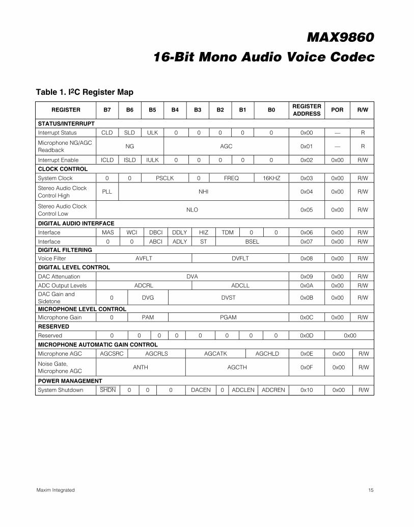
I2C RegistersThe MAX9860 audio codec is completely controlledthrough software using an I2C interface. The power-ondefault setting is software shutdown, requiring that theinternal registers be programmed to activate the device.See Table 1 for the device’s complete register map.
I2C Slave AddressThe MAX9860 responds to the slave address 0x20 forall write commands and 0x21 for all read operations.
MAX986016-Bit Mono Audio Voice Codec
15Maxim Integrated
REGISTER B7 B6 B5 B4 B3 B2 B1 B0REGISTERADDRESS
POR R/W
STATUS/INTERRUPT
Interrupt Status CLD SLD ULK 0 0 0 0 0 0x00 — R
Microphone NG/AGCReadback
NG AGC 0x01 — R
Interrupt Enable ICLD ISLD IULK 0 0 0 0 0 0x02 0x00 R/W
CLOCK CONTROL
System Clock 0 0 PSCLK 0 FREQ 16KHZ 0x03 0x00 R/W
Stereo Audio ClockControl High
PLL NHI 0x04 0x00 R/W
Stereo Audio ClockControl Low
NLO 0x05 0x00 R/W
DIGITAL AUDIO INTERFACE
Interface MAS WCI DBCI DDLY HIZ TDM 0 0 0x06 0x00 R/W
Interface 0 0 ABCI ADLY ST BSEL 0x07 0x00 R/WDIGITAL FILTERINGVoice Filter AVFLT DVFLT 0x08 0x00 R/W
DIGITAL LEVEL CONTROL
DAC Attenuation DVA 0x09 0x00 R/W
ADC Output Levels ADCRL ADCLL 0x0A 0x00 R/W
DAC Gain andSidetone
0 DVG DVST 0x0B 0x00 R/W
MICROPHONE LEVEL CONTROLMicrophone Gain 0 PAM PGAM 0x0C 0x00 R/W
RESERVED
Reserved 0 0 0 0 0 0 0 0 0x0D 0x00
MICROPHONE AUTOMATIC GAIN CONTROL
Microphone AGC AGCSRC AGCRLS AGCATK AGCHLD 0x0E 0x00 R/W
Noise Gate,Microphone AGC
ANTH AGCTH 0x0F 0x00 R/W
POWER MANAGEMENT
System Shutdown SHDN 0 0 0 DACEN 0 ADCLEN ADCREN 0x10 0x00 R/W
Table 1. I2C Register Map
MAX986016-Bit Mono Audio Voice Codec
16 Maxim Integrated
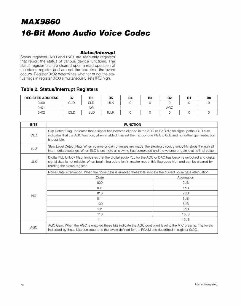
Status/InterruptStatus registers 0x00 and 0x01 are read-only registersthat report the status of various device functions. Thestatus register bits are cleared upon a read operation ofthe status register and are set the next time the eventoccurs. Register 0x02 determines whether or not the sta-tus flags in register 0x00 simultaneously sets IRQ high.
Table 2. Status/Interrupt Registers
REGISTER ADDRESS B7 B6 B5 B4 B3 B2 B1 B00x00 CLD SLD ULK 0 0 0 0 00x01 NG AGC0x02 ICLD ISLD IULK 0 0 0 0 0
BITS FUNCTION
CLDClip Detect Flag. Indicates that a signal has become clipped in the ADC or DAC digital signal paths. CLD alsoindicates that the AGC function, when enabled, has set the microphone PGA to 0dB and no further gain reductionis possible.
SLDSlew Level Detect Flag. When volume or gain changes are made, the slewing circuitry smoothly steps through allintermediate settings. When SLD is set high, all slewing has completed and the volume or gain is at its final value.
ULKDigital PLL Unlock Flag. Indicates that the digital audio PLL for the ADC or DAC has become unlocked and digitalsignal data is not reliable. When beginning operation in master mode, this flag goes high and can be cleared byreading the status register.
Noise Gate Attenuation. When the noise gate is enabled these bits indicate the current noise gate attenuation.
Code Attenuation
000 0dB
001 1dB
010 2dB
011 3dB
100 6dB
101 8dB
110 10dB
NG
111 12dB
AGCAGC Gain. When the AGC is enabled these bits indicate the AGC controlled level to the MIC preamp. The levelsindicated by these bits correspond to the levels defined for the PGAM bits described in register 0x0C.

MAX986016-Bit Mono Audio Voice Codec
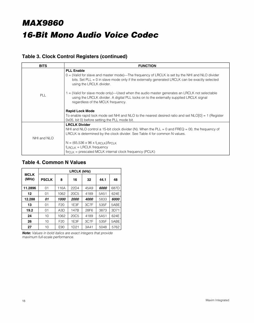
17Maxim Integrated
Clock ControlThe MAX9860 can work with a master clock (MCLK)supplied from any system clock within the range of10MHz to 60MHz. Internally, the MAX9860 requires a10MHz to 20MHz clock so a prescaler divides by 1, 2,or 4 to create the internal clock (PCLK). PCLK is usedto clock all portions of the MAX9860.
The MAX9860 is capable of supporting any sample ratefrom 8kHz to 48kHz, including all common sample rates(8kHz, 16kHz, 24kHz, 32kHz, 44.1kHz, 48kHz). Toaccommodate a wide range of system architectures,the MAX9860 supports three main clocking modes:
Normal Mode: This mode uses a 15-bit clock dividercoefficient to set the sample rate relative to the
prescaled MCLK input (PCLK). This allows high flexibili-ty in both the MCLK and LRCLK frequencies and canbe used in either master or slave mode.
Exact Integer Mode: Common MCLK frequencies(12MHz, 13MHz, and 19.2MHz) can be programmed tooperate in exact integer mode for both 8kHz and 16kHzsample rates. In these modes, the MCLK and LRCLKrates are selected by using the FREQ and 16KHZ bitsinstead of the NHI, NLO, and PLL control bits.
PLL Mode: When operating in slave mode, a PLL canbe enabled to lock onto externally generated LRCLKsignals that are asynchronously related to PCLK.
Table 3. Clock Control Registers
REGISTER ADDRESS B7 B6 B5 B4 B3 B2 B1 B00x03 0 0 PSCLK 0 FREQ 16KHZ0x04 PLL NHI0x05 NLO
BITS FUNCTION
PSCLK[1:0]
MCLK PrescalerDivides MCLK down to generate a PCLK between 10MHz and 20MHz.
00 = Disable clock for low-power shutdown.01 = Select if MCLK is between 10MHz and 20MHz.10 = Select if MCLK is between 20MHz and 40MHz.11 = Select if MCLK is greater than 40MHz.
FREQ[1:0]
Integer Clock ModeEnables exact integer mode for three predefined PCLK frequencies. Exact integer mode is normallyintended for master mode, but can be enabled in slave mode if the externally supplied LRCLK exactlymatches the frequency specified in each mode.
00 = Normal operation (configure clocking with the PLL, NHI, and NLO bits).01 = Select when PCLK is 12MHz (LRCLK = PCLK/1500 or PCLK/750).10 = Select when PCLK is 13MHz (LRCLK = PCLK/1625 or PCLK/812.5).11 = Select when PCLK is 19.2MHz (LRCLK = PCLK/2400 or PCLK/1200).
When FREQ ≠ 00, the PLL, NHI, and NLO bits are unused.
16KHZ
16kHz ModeWhen FREQ ≠ 00:0 = LRCLK is exactly 8kHz.1 = LRCLK is exactly 16kHz.
When FREQ = 00, 16KHZ is used to set the AGC clock rate:0 = Use when LRCLK ≤ 24kHz.1 = Use when LRCLK > 24kHz.
MAX986016-Bit Mono Audio Voice Codec
18 Maxim Integrated
Table 3. Clock Control Registers (continued)
BITS FUNCTION
PLL
PLL Enable0 = (Valid for slave and master mode)—The frequency of LRCLK is set by the NHI and NLO divider bits. Set PLL = 0 in slave mode only if the externally generated LRCLK can be exactly selected using the LRCLK divider.
1 = (Valid for slave mode only)—Used when the audio master generates an LRCLK not selectable using the LRCLK divider. A digital PLL locks on to the externally supplied LRCLK signal regardless of the MCLK frequency.
Rapid Lock ModeTo enable rapid lock mode set NHI and NLO to the nearest desired ratio and set NLO[0] = 1 (Register0x05, bit 0) before setting the PLL mode bit.
NHI and NLO
LRCLK DividerNHI and NLO control a 15-bit clock divider (N). When the PLL = 0 and FREQ = 00, the frequency ofLRCLK is determined by the clock divider. See Table 4 for common N values.
N = (65,536 x 96 x fLRCLK)/fPCLKfLRCLK = LRCLK frequencyfPCLK = prescaled MCLK internal clock frequency (PCLK)
LRCLK (kHz)MCLK(MHz) PSCLK 8 16 32 44.1 48
11.2896 01 116A 22D4 45A9 6000 687D
12 01 1062 20C5 4189 5A51 624E
12.288 01 1000 2000 4000 5833 6000
13 01 F20 1E3F 3C7F 535F 5ABE
19.2 01 A3D 147B 28F6 3873 3D71
24 10 1062 20C5 4189 5A51 624E
26 10 F20 1E3F 3C7F 535F 5ABE
27 10 E90 1D21 3A41 5048 5762
Table 4. Common N Values
Note: Values in bold italics are exact integers that providemaximum full-scale performance.
MAX986016-Bit Mono Audio Voice Codec
19Maxim Integrated
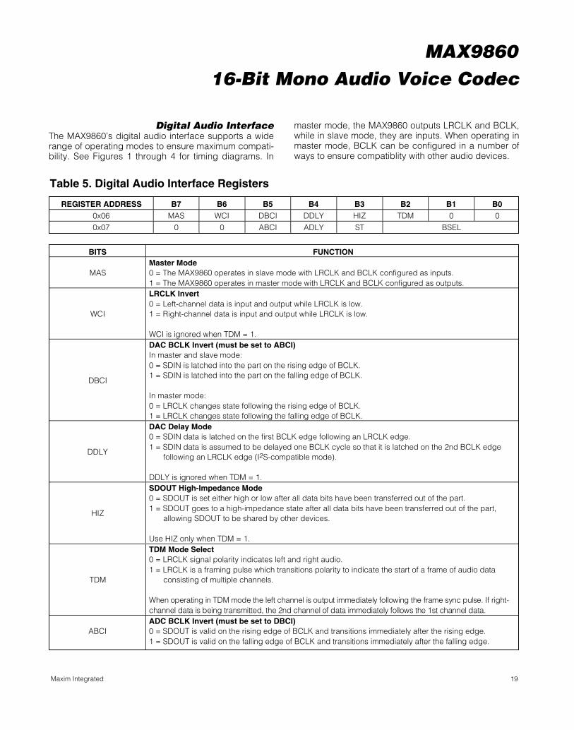
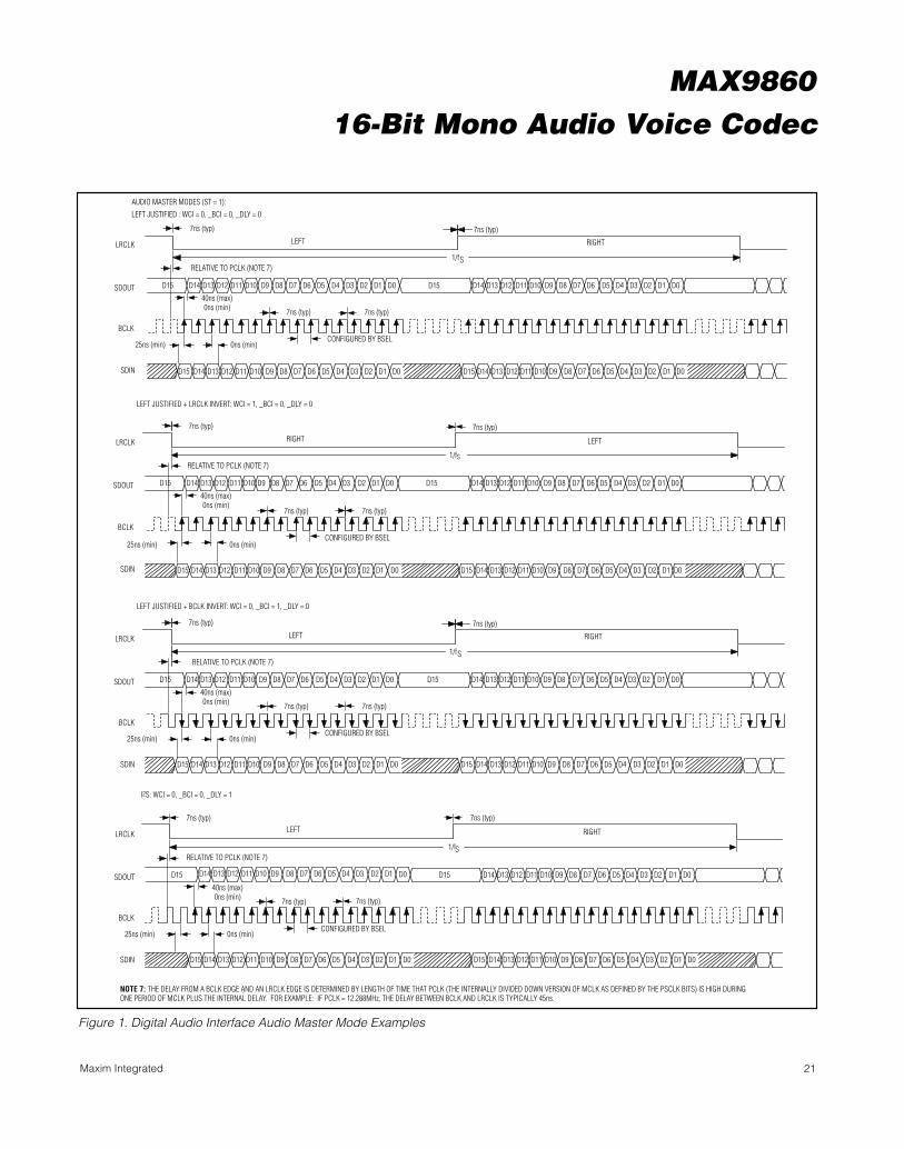
Digital Audio InterfaceThe MAX9860’s digital audio interface supports a widerange of operating modes to ensure maximum compati-bility. See Figures 1 through 4 for timing diagrams. In
master mode, the MAX9860 outputs LRCLK and BCLK,while in slave mode, they are inputs. When operating inmaster mode, BCLK can be configured in a number ofways to ensure compatiblity with other audio devices.
Table 5. Digital Audio Interface Registers
REGISTER ADDRESS B7 B6 B5 B4 B3 B2 B1 B00x06 MAS WCI DBCI DDLY HIZ TDM 0 00x07 0 0 ABCI ADLY ST BSEL
BITS FUNCTION
MASMaster Mode0 = The MAX9860 operates in slave mode with LRCLK and BCLK configured as inputs.1 = The MAX9860 operates in master mode with LRCLK and BCLK configured as outputs.
WCI
LRCLK Invert0 = Left-channel data is input and output while LRCLK is low.1 = Right-channel data is input and output while LRCLK is low.
WCI is ignored when TDM = 1.
DBCI
DAC BCLK Invert (must be set to ABCI)In master and slave mode:0 = SDIN is latched into the part on the rising edge of BCLK.1 = SDIN is latched into the part on the falling edge of BCLK.
In master mode:0 = LRCLK changes state following the rising edge of BCLK.1 = LRCLK changes state following the falling edge of BCLK.
DDLY
DAC Delay Mode0 = SDIN data is latched on the first BCLK edge following an LRCLK edge.1 = SDIN data is assumed to be delayed one BCLK cycle so that it is latched on the 2nd BCLK edge following an LRCLK edge (I2S-compatible mode).
DDLY is ignored when TDM = 1.
HIZ
SDOUT High-Impedance Mode0 = SDOUT is set either high or low after all data bits have been transferred out of the part.1 = SDOUT goes to a high-impedance state after all data bits have been transferred out of the part, allowing SDOUT to be shared by other devices.
Use HIZ only when TDM = 1.
TDM
TDM Mode Select0 = LRCLK signal polarity indicates left and right audio.1 = LRCLK is a framing pulse which transitions polarity to indicate the start of a frame of audio data consisting of multiple channels.
W hen op er ati ng i n TD M m od e the l eft channel i s outp ut i m m ed i atel y fol l ow i ng the fr am e sync p ul se. If r i g ht- channel d ata i s b ei ng tr ansm i tted , the 2nd channel of d ata i m m ed i atel y fol l ow s the 1st channel d ata.
ABCIADC BCLK Invert (must be set to DBCI)0 = SDOUT is valid on the rising edge of BCLK and transitions immediately after the rising edge.1 = SDOUT is valid on the falling edge of BCLK and transitions immediately after the falling edge.
MAX986016-Bit Mono Audio Voice Codec
20 Maxim Integrated
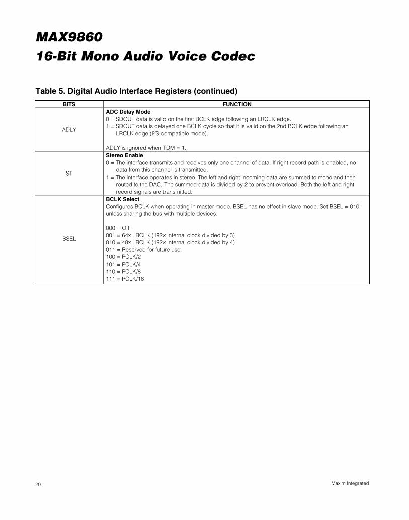
Table 5. Digital Audio Interface Registers (continued)
BITS FUNCTION
ADLY
ADC Delay Mode0 = SDOUT data is valid on the first BCLK edge following an LRCLK edge.1 = SDOUT data is delayed one BCLK cycle so that it is valid on the 2nd BCLK edge following an LRCLK edge (I2S-compatible mode).
ADLY is ignored when TDM = 1.
ST
Stereo Enable0 = The interface transmits and receives only one channel of data. If right record path is enabled, no data from this channel is transmitted.1 = The interface operates in stereo. The left and right incoming data are summed to mono and then routed to the DAC. The summed data is divided by 2 to prevent overload. Both the left and right record signals are transmitted.
BSEL
BCLK SelectConfigures BCLK when operating in master mode. BSEL has no effect in slave mode. Set BSEL = 010,unless sharing the bus with multiple devices.
000 = Off001 = 64x LRCLK (192x internal clock divided by 3)010 = 48x LRCLK (192x internal clock divided by 4)011 = Reserved for future use.100 = PCLK/2101 = PCLK/4110 = PCLK/8111 = PCLK/16
MAX986016-Bit Mono Audio Voice Codec
21Maxim Integrated
LEFT
LEFT JUSTIFIED : WCI = 0, _BCI = 0, _DLY = 0
AUDIO MASTER MODES (ST = 1):
LEFT JUSTIFIED + LRCLK INVERT: WCI = 1, _BCI = 0, _DLY = 0
LEFT JUSTIFIED + BCLK INVERT: WCI = 0, _BCI = 1, _DLY = 0
I2S: WCI = 0, _BCI = 0, _DLY = 1
LRCLK
BCLK
SDOUT
SDIN
D14 D13 D12 D11 D10 D9 D8 D7 D6 D5 D4 D3 D2 D1 D0 D14 D13 D12 D11 D10 D9 D8 D7 D6 D5 D4 D3 D2 D1 D0
1/fS
CONFIGURED BY BSEL
7ns (typ)
7ns (typ)
D14 D13 D12 D11 D10 D9 D8 D7 D6 D5 D4 D3 D2 D1 D0 D14 D13 D12 D11 D10 D9 D8 D7 D6 D5 D4 D3 D2 D1 D0D15D15
25ns (min)
7ns (typ)
7ns (typ)
0ns (min)
40ns (max)0ns (min)
RELATIVE TO PCLK (NOTE 7)
RIGHT
RIGHTLRCLK
BCLK
SDOUT
SDIN
D14 D13 D12 D11 D10 D9 D8 D7 D6 D5 D4 D3 D2 D1 D0 D14 D13 D12 D11 D10 D9 D8 D7 D6 D5 D4 D3 D2 D1 D0
1/fS
CONFIGURED BY BSEL
7ns (typ)
7ns (typ)
D14 D13 D12 D11 D10 D9 D8 D7 D6 D5 D4 D3 D2 D1 D0 D14 D13 D12 D11 D10 D9 D8 D7 D6 D5 D4 D3 D2 D1 D0D15D15
25ns (min)
7ns (typ)
7ns (typ)
0ns (min)
40ns (max)0ns (min)
RELATIVE TO PCLK (NOTE 7)
LEFT
LEFTLRCLK
BCLK
SDOUT
SDIN
D14 D13 D12 D11 D10 D9 D8 D7 D6 D5 D4 D3 D2 D1 D0 D14 D13 D12 D11 D10 D9 D8 D7 D6 D5 D4 D3 D2 D1 D0
1/fS
CONFIGURED BY BSEL
7ns (typ)
7ns (typ)
D14 D13 D12 D11 D10 D9 D8 D7 D6 D5 D4 D3 D2 D1 D0 D14 D13 D12 D11 D10 D9 D8 D7 D6 D5 D4 D3 D2 D1 D0D15D15
25ns (min)
7ns (typ)
7ns (typ)
0ns (min)
40ns (max)0ns (min)
RELATIVE TO PCLK (NOTE 7)
RIGHT
LEFTLRCLK
BCLK
SDOUT
SDIN
D14 D13 D12 D11 D10 D9 D8 D7 D6 D5 D4 D3 D2 D1 D14 D13 D12 D11 D10 D9 D8 D7 D6 D5 D4 D3 D2 D1
1/fS
CONFIGURED BY BSEL
7ns (typ)
7ns (typ)
D14 D13 D12 D11 D10 D9 D8 D7 D6 D5 D4 D3 D2 D1 D0 D14 D13 D12 D11 D10 D9 D8 D7 D6 D5 D4 D3 D2 D1 D0D15D15
25ns (min)
7ns (typ)
7ns (typ)
0ns (min)
40ns (max)0ns (min)
RELATIVE TO PCLK (NOTE 7)
RIGHT
D0
D15
D15
D15
D15
D15
D15
D15
NOTE 7: THE DELAY FROM A BCLK EDGE AND AN LRCLK EDGE IS DETERMINED BY LENGTH OF TIME THAT PCLK (THE INTERNALLY DIVIDED DOWN VERSION OF MCLK AS DEFINED BY THE PSCLK BITS) IS HIGH DURINGONE PERIOD OF MCLK PLUS THE INTERNAL DELAY. FOR EXAMPLE: IF PCLK = 12.288MHz, THE DELAY BETWEEN BCLK AND LRCLK IS TYPICALLY 45ns.
D15 D0
Figure 1. Digital Audio Interface Audio Master Mode Examples
MAX986016-Bit Mono Audio Voice Codec
22 Maxim Integrated
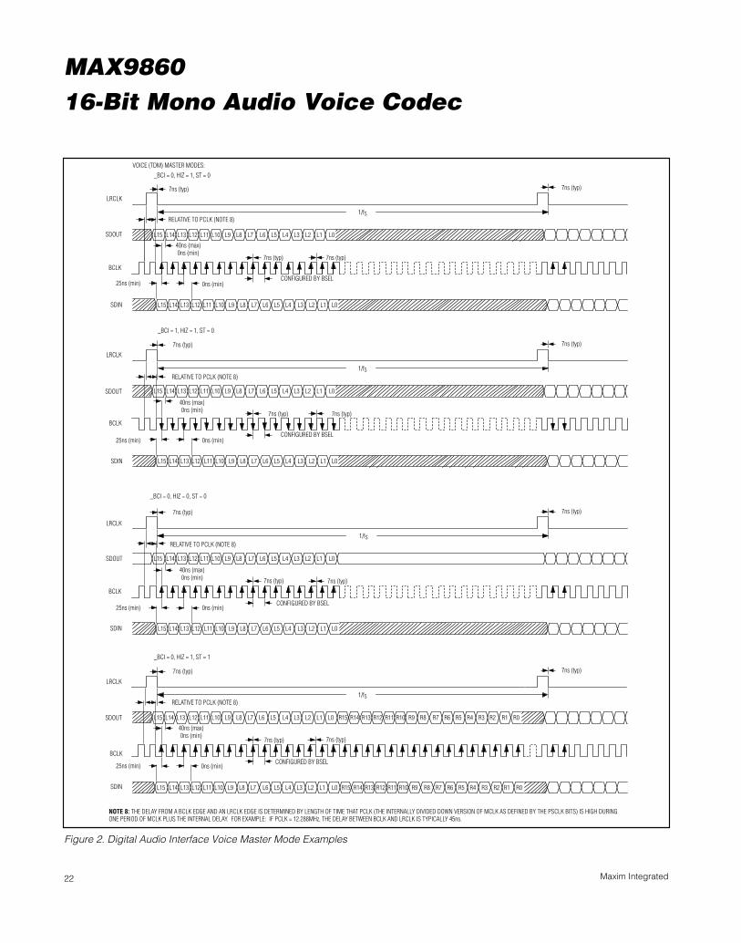
VOICE (TDM) MASTER MODES:
LRCLK
BCLK
SDOUT
SDIN
L14 L13 L12 L11 L10 L9 L8 L7 L6 L5 L4 L3 L2 L1 L0
1/fS
CONFIGURED BY BSEL
7ns (typ)
7ns (typ)
L14 L13 L12 L11 L10 L9 L8 L7 L6 L5 L4 L3 L2 L1 L0L15
25ns (min)
7ns (typ)
7ns (typ)
0ns (min)
40ns (max)0ns (min)
L15
RELATIVE TO PCLK (NOTE 8)
_BCI = 0, HIZ = 1, ST = 0
_BCI = 1, HIZ = 1, ST = 0
_BCI = 0, HIZ = 0, ST = 0
LRCLK
BCLK
SDOUT
SDIN
L14 L13 L12 L11 L10 L9 L8 L7 L6 L5 L4 L3 L2 L1 L0
1/fS
CONFIGURED BY BSEL
7ns (typ)
7ns (typ)
L14 L13 L12 L11 L10 L9 L8 L7 L6 L5 L4 L3 L2 L1 L0L15
25ns (min)
7ns (typ)
7ns (typ)
0ns (min)
40ns (max)0ns (min)
L15
RELATIVE TO PCLK (NOTE 8)
LRCLK
BCLK
SDOUT
SDIN
L14 L13 L12 L11 L10 L9 L8 L7 L6 L5 L4 L3 L2 L1 L0
1/fS
CONFIGURED BY BSEL
7ns (typ)
7ns (typ)
L14 L13 L12 L11 L10 L9 L8 L7 L6 L5 L4 L3 L2 L1 L0L15
25ns (min)
7ns (typ)
7ns (typ)
0ns (min)
40ns (max)0ns (min)
L15
RELATIVE TO PCLK (NOTE 8)
LRCLK
BCLK
SDOUT
SDIN
L14 L13 L12 L11 L10 L9 L8 L7 L6 L5 L4 L3 L2 L1 L0
1/fS
CONFIGURED BY BSEL
7ns (typ)
7ns (typ)
L14 L13 L12 L11 L10 L9 L8 L7 L6 L5 L4 L3 L2 L1 L0L15
25ns (min)
7ns (typ)
7ns (typ)
0ns (min)
40ns (max)0ns (min)
L15
RELATIVE TO PCLK (NOTE 8)
_BCI = 0, HIZ = 1, ST = 1
R14 R13 R12 R11 R10 R9 R8 R7 R6 R5 R4 R3 R2 R1 R0R15
R14 R13 R12 R11 R10 R9 R8 R7 R6 R5 R4 R3 R2 R1 R0R15
NOTE 8: THE DELAY FROM A BCLK EDGE AND AN LRCLK EDGE IS DETERMINED BY LENGTH OF TIME THAT PCLK (THE INTERNALLY DIVIDED DOWN VERSION OF MCLK AS DEFINED BY THE PSCLK BITS) IS HIGH DURINGONE PERIOD OF MCLK PLUS THE INTERNAL DELAY. FOR EXAMPLE: IF PCLK = 12.288MHz, THE DELAY BETWEEN BCLK AND LRCLK IS TYPICALLY 45ns.
Figure 2. Digital Audio Interface Voice Master Mode Examples
MAX986016-Bit Mono Audio Voice Codec
23Maxim Integrated
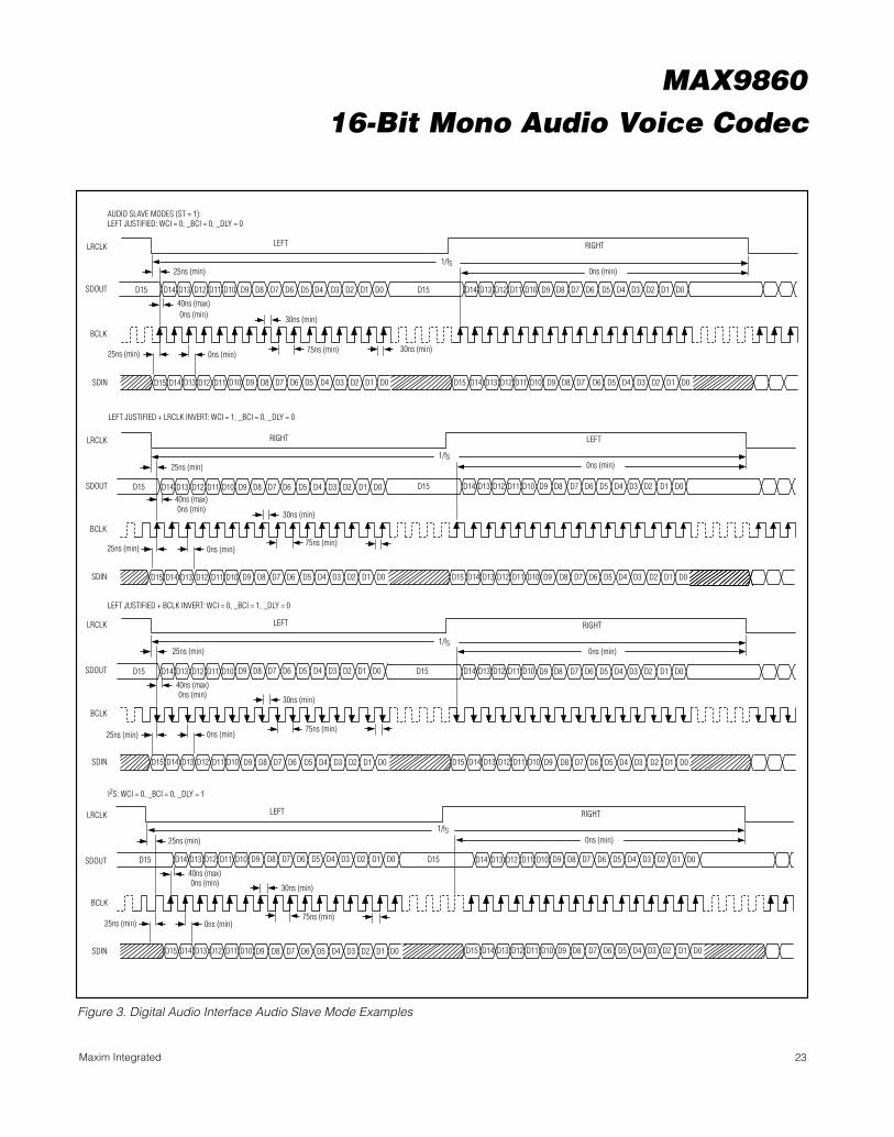
LEFT
AUDIO SLAVE MODES (ST = 1):LEFT JUSTIFIED: WCI = 0, _BCI = 0, _DLY = 0
LEFT JUSTIFIED + LRCLK INVERT: WCI = 1, _BCI = 0, _DLY = 0
LEFT JUSTIFIED + BCLK INVERT: WCI = 0, _BCI = 1, _DLY = 0
I2S: WCI = 0, _BCI = 0, _DLY = 1
LRCLK
BCLK
SDOUT
SDIN
D14 D13 D12 D11 D10 D9 D8 D7 D6 D5 D4 D3 D2 D1 D0 D14 D13 D12 D11 D10 D9 D8 D7 D6 D5 D4 D3 D2 D1 D0
1/fS
75ns (min)
D14 D13 D12 D11 D10 D9 D8 D7 D6 D5 D4 D3 D2 D1 D0 D14 D13 D12 D11 D10 D9 D8 D7 D6 D5 D4 D3 D2 D1 D0D15D15
25ns (min) 0ns (min)
40ns (max)0ns (min)
RIGHT
RIGHTLRCLK
BCLK
SDOUT
SDIN
D14 D13 D12 D11 D10 D9 D8 D7 D6 D5 D4 D3 D2 D1 D0 D14 D13 D12 D11 D10 D9 D8 D7 D6 D5 D4 D3 D2 D1 D0
1/fS
D14 D13 D12 D11 D10 D9 D8 D7 D6 D5 D4 D3 D2 D1 D0 D14 D13 D12 D11 D10 D9 D8 D7 D6 D5 D4 D3 D2 D1 D0D15D15
25ns (min) 0ns (min)
40ns (max)0ns (min)
LEFT
LEFTLRCLK
BCLK
SDOUT
SDIN
D14 D13 D12 D11 D10 D9 D8 D7 D6 D5 D4 D3 D2 D1 D0 D14 D13 D12 D11 D10 D9 D8 D7 D6 D5 D4 D3 D2 D1 D0
1/fS
D14 D13 D12 D11 D10 D9 D8 D7 D6 D5 D4 D3 D2 D1 D0 D14 D13 D12 D11 D10 D9 D8 D7 D6 D5 D4 D3 D2 D1 D0D15D15
25ns (min) 0ns (min)
40ns (max)0ns (min)
RIGHT
LEFTLRCLK
BCLK
SDOUT
SDIN
D14 D13 D12 D11 D10 D9 D8 D7 D6 D5 D4 D3 D2 D1 D14 D13 D12 D11 D10 D9 D8 D7 D6 D5 D4 D3 D2 D1
1/fS
D14 D13 D12 D11 D10 D9 D8 D7 D6 D5 D4 D3 D2 D1 D0 D14 D13 D12 D11 D10 D9 D8 D7 D6 D5 D4 D3 D2 D1 D0D15D15
25ns (min) 0ns (min)
RIGHT
D15D15
D15
D15
D15
D15
30ns (min)
30ns (min)
25ns (min)
75ns (min)
30ns (min)
25ns (min)
75ns (min)
30ns (min)
25ns (min)
75ns (min)
30ns (min)
25ns (min)
0ns (min)
0ns (min)
0ns (min)
0ns (min)
40ns (max)0ns (min)
D15 D0 D15 D0
Figure 3. Digital Audio Interface Audio Slave Mode Examples
MAX986016-Bit Mono Audio Voice Codec
24 Maxim Integrated
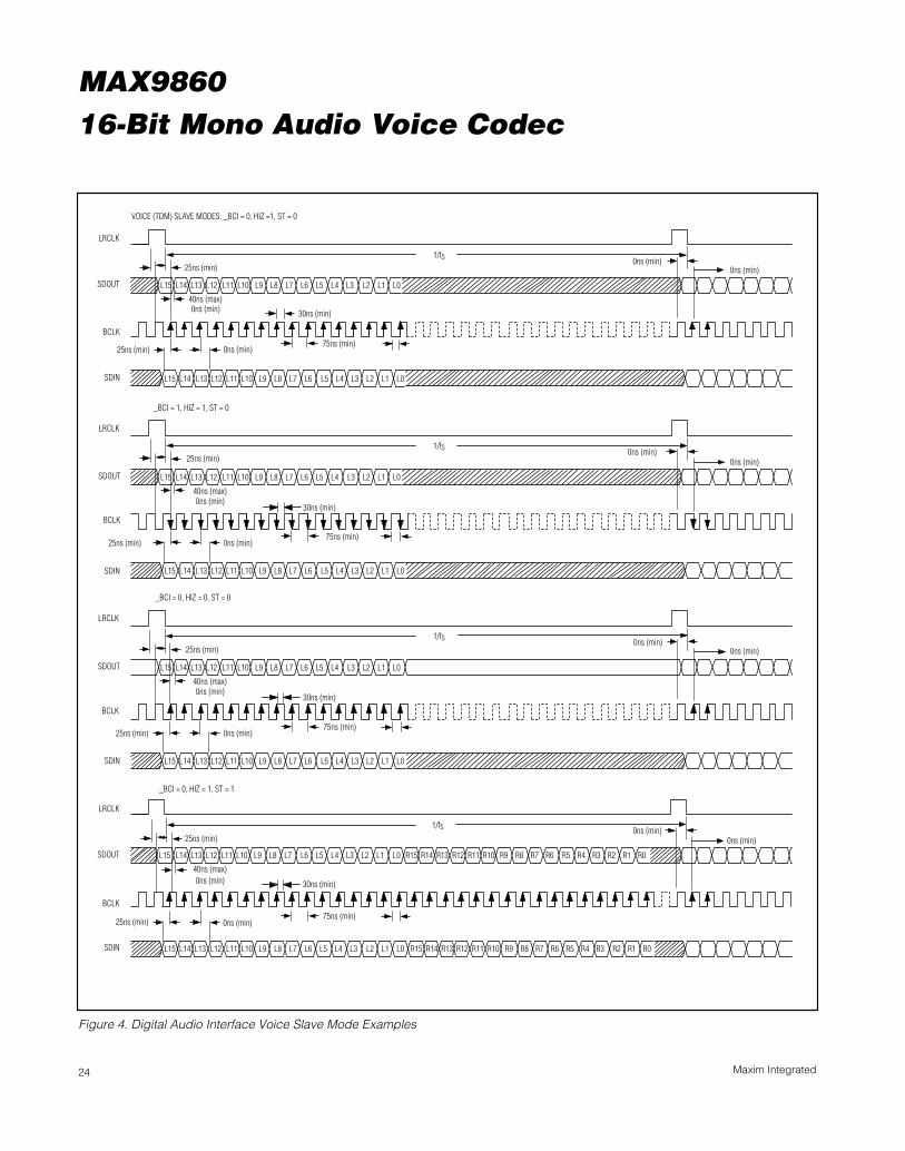
LRCLK
BCLK
SDOUT
SDIN
L14 L13 L12 L11 L10 L9 L8 L7 L6 L5 L4 L3 L2 L1 L0
1/fS
L14 L13 L12 L11 L10 L9 L8 L7 L6 L5 L4 L3 L2 L1 L0L15
25ns (min) 0ns (min)
40ns (max)0ns (min)
L15
VOICE (TDM) SLAVE MODES: _BCI = 0, HIZ =1, ST = 0
_BCI = 1, HIZ = 1, ST = 0
_BCI = 0, HIZ = 0, ST = 0
LRCLK
BCLK
SDOUT
SDIN
L14 L13 L12 L11 L10 L9 L8 L7 L6 L5 L4 L3 L2 L1 L0
L14 L13 L12 L11 L10 L9 L8 L7 L6 L5 L4 L3 L2 L1 L0L15
25ns (min) 0ns (min)
40ns (max)0ns (min)
L15
LRCLK
BCLK
SDOUT
SDIN
L14 L13 L12 L11 L10 L9 L8 L7 L6 L5 L4 L3 L2 L1 L0
L14 L13 L12 L11 L10 L9 L8 L7 L6 L5 L4 L3 L2 L1 L0L15
25ns (min) 0ns (min)
40ns (max)0ns (min)
L15
75ns (min)
30ns (min)
25ns (min)
75ns (min)
30ns (min)
75ns (min)
30ns (min)
0ns (min)0ns (min)
1/fS25ns (min)
0ns (min)0ns (min)
1/fS25ns (min)
0ns (min)0ns (min)
LRCLK
BCLK
SDOUT
SDIN
L14 L13 L12 L11 L10 L9 L8 L7 L6 L5 L4 L3 L2 L1 L0
1/fS
L14 L13 L12 L11 L10 L9 L8 L7 L6 L5 L4 L3 L2 L1 L0L15
25ns (min) 0ns (min)
40ns (max)0ns (min)
L15
_BCI = 0, HIZ = 1, ST = 1
75ns (min)
30ns (min)
25ns (min)0ns (min)
0ns (min)
R14 R13 R12 R11 R10 R9 R8 R7 R6 R5 R4 R3 R2 R1 R0R15
R14 R13 R12 R11 R10 R9 R8 R7 R6 R5 R4 R3 R2 R1 R0R15
Figure 4. Digital Audio Interface Voice Slave Mode Examples
MAX986016-Bit Mono Audio Voice Codec
25Maxim Integrated
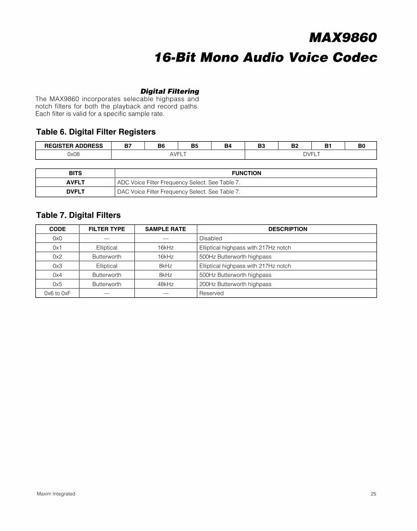
Digital FilteringThe MAX9860 incorporates selecable highpass andnotch filters for both the playback and record paths.Each filter is valid for a specific sample rate.
Table 6. Digital Filter Registers
REGISTER ADDRESS B7 B6 B5 B4 B3 B2 B1 B00x08 AVFLT DVFLT
BITS FUNCTION
AVFLT ADC Voice Filter Frequency Select. See Table 7.
DVFLT DAC Voice Filter Frequency Select. See Table 7.
Table 7. Digital Filters
CODE FILTER TYPE SAMPLE RATE DESCRIPTION
0x0 — — Disabled
0x1 Elliptical 16kHz Elliptical highpass with 217Hz notch
0x2 Butterworth 16kHz 500Hz Butterworth highpass
0x3 Elliptical 8kHz Elliptical highpass with 217Hz notch
0x4 Butterworth 8kHz 500Hz Butterworth highpass
0x5 Butterworth 48kHz 200Hz Butterworth highpass
0x6 to 0xF — — Reserved
MAX986016-Bit Mono Audio Voice Codec
26 Maxim Integrated
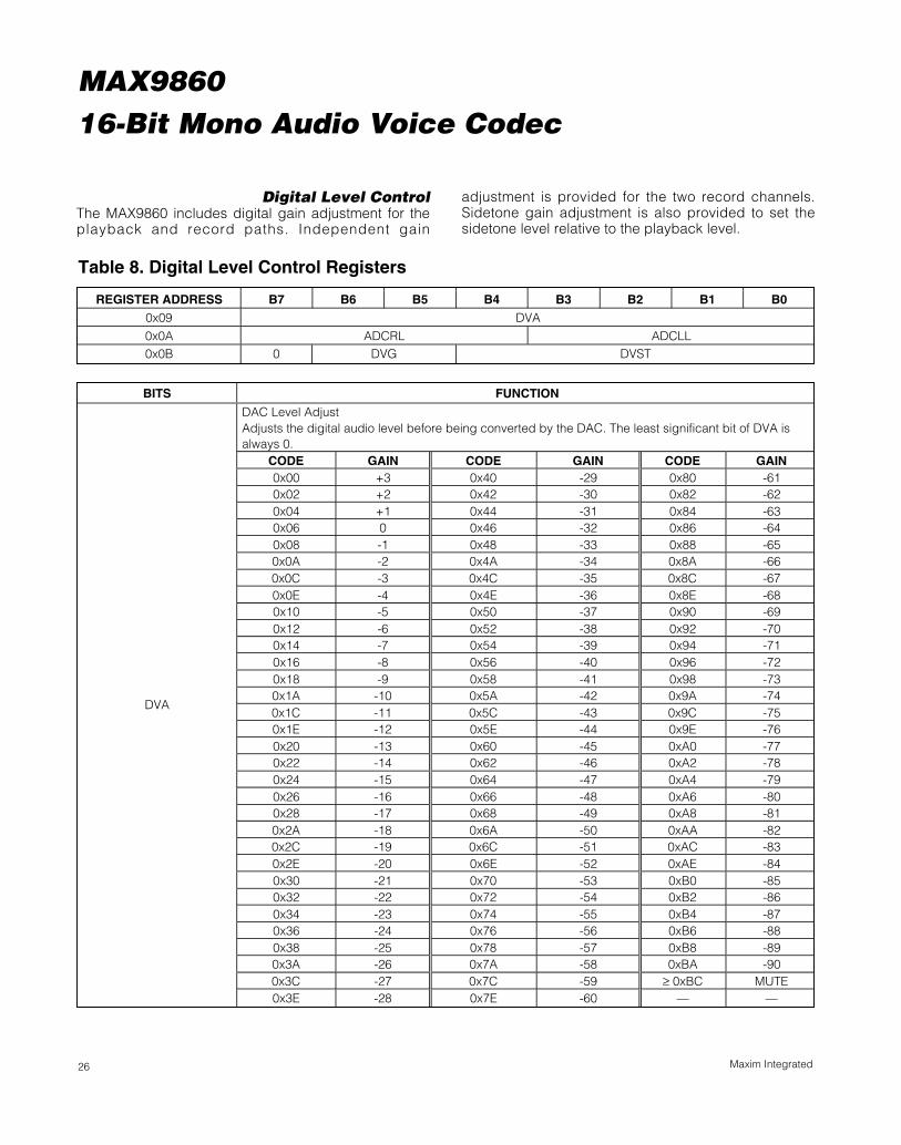
Digital Level ControlThe MAX9860 includes digital gain adjustment for theplayback and record paths. Independent gain
adjustment is provided for the two record channels.Sidetone gain adjustment is also provided to set thesidetone level relative to the playback level.
Table 8. Digital Level Control Registers
REGISTER ADDRESS B7 B6 B5 B4 B3 B2 B1 B00x09 DVA0x0A ADCRL ADCLL0x0B 0 DVG DVST
BITS FUNCTION
DAC Level AdjustAdjusts the digital audio level before being converted by the DAC. The least significant bit of DVA isalways 0.
CODE GAIN CODE GAIN CODE GAIN0x00 +3 0x40 -29 0x80 -610x02 +2 0x42 -30 0x82 -620x04 +1 0x44 -31 0x84 -630x06 0 0x46 -32 0x86 -640x08 -1 0x48 -33 0x88 -650x0A -2 0x4A -34 0x8A -660x0C -3 0x4C -35 0x8C -670x0E -4 0x4E -36 0x8E -680x10 -5 0x50 -37 0x90 -690x12 -6 0x52 -38 0x92 -700x14 -7 0x54 -39 0x94 -710x16 -8 0x56 -40 0x96 -720x18 -9 0x58 -41 0x98 -730x1A -10 0x5A -42 0x9A -740x1C -11 0x5C -43 0x9C -750x1E -12 0x5E -44 0x9E -760x20 -13 0x60 -45 0xA0 -770x22 -14 0x62 -46 0xA2 -780x24 -15 0x64 -47 0xA4 -790x26 -16 0x66 -48 0xA6 -800x28 -17 0x68 -49 0xA8 -810x2A -18 0x6A -50 0xAA -820x2C -19 0x6C -51 0xAC -830x2E -20 0x6E -52 0xAE -840x30 -21 0x70 -53 0xB0 -850x32 -22 0x72 -54 0xB2 -860x34 -23 0x74 -55 0xB4 -870x36 -24 0x76 -56 0xB6 -880x38 -25 0x78 -57 0xB8 -890x3A -26 0x7A -58 0xBA -900x3C -27 0x7C -59 ≥ 0xBC MUTE
DVA
0x3E -28 0x7E -60 — —
MAX986016-Bit Mono Audio Voice Codec
27Maxim Integrated
Table 8. Digital Level Control Registers (continued)
BITS FUNCTION
Left and Right ADC Output LevelAdjusts the digital audio level output by the ADCs.
CODE GAIN0x0 +30x1 +20x2 +10x3 00x4 -10x5 -20x6 -30x7 -40x8 -50x9 -60xA -70xB -80xC -80xD -100xE -11
ADCRL/ADCLL
0xF -12DAC GainThe gain set by DVG adds to the level set by DVA.
CODE GAIN00 001 +610 +12
DVG
11 +18SidetoneSets the level of left ADC output mixed into the DAC.
CODE GAIN CODE GAIN0x00 Disabled 0x10 -300x01 0 0x11 -320x02 -2 0x12 -340x03 -4 0x13 -360x04 -6 0x14 -380x05 -8 0x15 -400x06 -10 0x16 -420x07 -12 0x17 -440x08 -14 0x18 -460x09 -16 0x19 -480x0A -18 0x1A -500x0B -20 0x1B -520x0C -22 0x1C -540x0D -24 0x1D -560x0E -26 0x1E -58
DVST
0x0F -28 0x1F -60

MAX986016-Bit Mono Audio Voice Codec
28 Maxim Integrated
Microphone InputsThe MAX9860 provides two differential microphoneinputs and a low-noise 1.55V microphone bias for power-ing the microphones. In typical applications, the leftmicrophone is used to record a voice signal and theright microphone is used to record a background noisesignal. In applications that require only one microphone,use the left microphone input and disable the right ADC.The microphone signals are amplified by two stages of
gain and then routed to the ADCs. The first stage offersselectable 0dB, 20dB, or 30dB settings. The secondstage is a programmable gain amplifier (PGA) adjustablefrom 0dB to 20dB in 1dB steps. Zero-crossing detectionis included on the PGA to minimize zipper noise whilemaking gain changes. See Figure 5 for a detailed dia-gram of the microphone input structure.
MICLN
MICLP
MICBIAS
AGC
PGA
PGA
-
PREAMP
MICRN
ADCL
ADCR
MICRP
REG1.55V
0/20/30dB
0dB to +20dB
0dB to +20dB
VCM
VCM
0/20/30dB
MICGND
PREAMP
MAX9860
Figure 5. Microphone Input Block Diagram
MAX986016-Bit Mono Audio Voice Codec
29Maxim Integrated
Table 9. Microphone Input Register
REGISTER ADDRESS B7 B6 B5 B4 B3 B2 B1 B00x0C 0 PAM PGAM
BITS FUNCTIONLeft and Right Microphone Preamp Gain
CODE GAIN (dB)00 Disabled01 010 +2011 +30
PAM
Note: Selecting 00 disables the microphone inputs and microphone bias automatically.Left and Right Microphone PGA
CODE GAIN (dB) CODE GAIN (dB)0x00 +20 0x0B +90x01 +19 0x0C +80x02 +18 0x0D +70x03 +17 0x0E +60x04 +16 0x0F +50x05 +15 0x10 +40x06 +14 0x11 +30x07 +13 0x12 +20x08 +12 0x13 +10x09 +11 ≥ 0x14 00x0A +10 — —
PGAM
Note: When AGC is enabled, the AGC controller overrides these settings.
MAX986016-Bit Mono Audio Voice Codec
30 Maxim Integrated
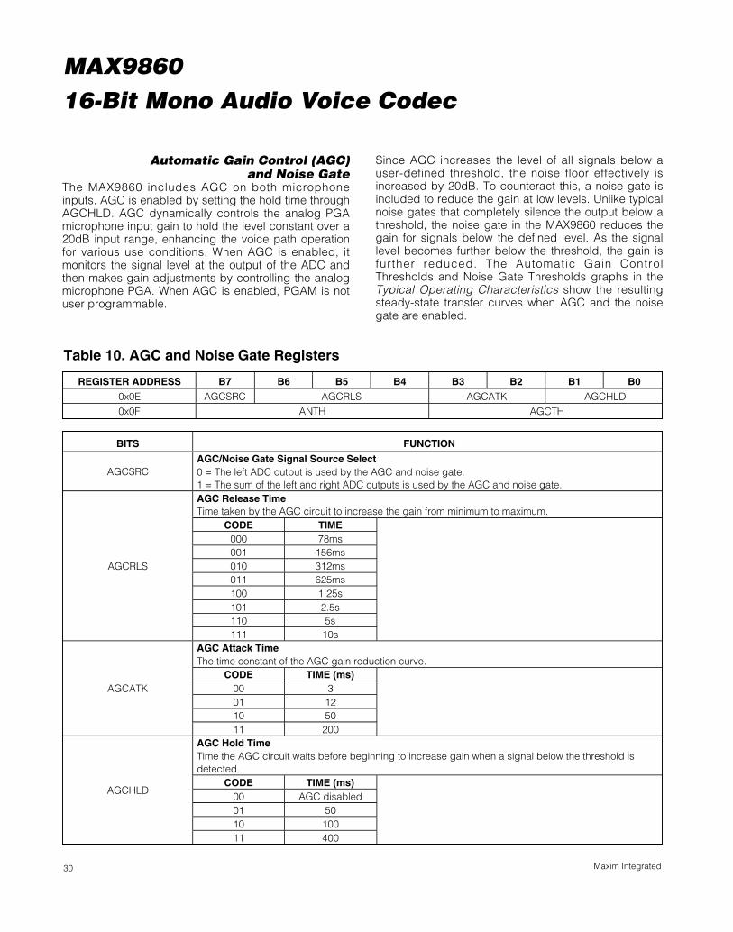
Automatic Gain Control (AGC)and Noise Gate
The MAX9860 includes AGC on both microphoneinputs. AGC is enabled by setting the hold time throughAGCHLD. AGC dynamically controls the analog PGAmicrophone input gain to hold the level constant over a20dB input range, enhancing the voice path operationfor various use conditions. When AGC is enabled, itmonitors the signal level at the output of the ADC andthen makes gain adjustments by controlling the analogmicrophone PGA. When AGC is enabled, PGAM is notuser programmable.
Since AGC increases the level of all signals below auser-defined threshold, the noise floor effectively isincreased by 20dB. To counteract this, a noise gate isincluded to reduce the gain at low levels. Unlike typicalnoise gates that completely silence the output below athreshold, the noise gate in the MAX9860 reduces thegain for signals below the defined level. As the signallevel becomes further below the threshold, the gain isfurther reduced. The Automatic Gain ControlThresholds and Noise Gate Thresholds graphs in theTypical Operating Characteristics show the resultingsteady-state transfer curves when AGC and the noisegate are enabled.
Table 10. AGC and Noise Gate Registers
REGISTER ADDRESS B7 B6 B5 B4 B3 B2 B1 B00x0E AGCSRC AGCRLS AGCATK AGCHLD0x0F ANTH AGCTH
BITS FUNCTION
AGCSRCAGC/Noise Gate Signal Source Select0 = The left ADC output is used by the AGC and noise gate.1 = The sum of the left and right ADC outputs is used by the AGC and noise gate.AGC Release TimeTime taken by the AGC circuit to increase the gain from minimum to maximum.
CODE TIME000 78ms001 156ms010 312ms011 625ms100 1.25s101 2.5s110 5s
AGCRLS
111 10sAGC Attack TimeThe time constant of the AGC gain reduction curve.
CODE TIME (ms)00 301 1210 50
AGCATK
11 200AGC Hold TimeTime the AGC circuit waits before beginning to increase gain when a signal below the threshold isdetected.
CODE TIME (ms)00 AGC disabled01 5010 100
AGCHLD
11 400
MAX986016-Bit Mono Audio Voice Codec
31Maxim Integrated
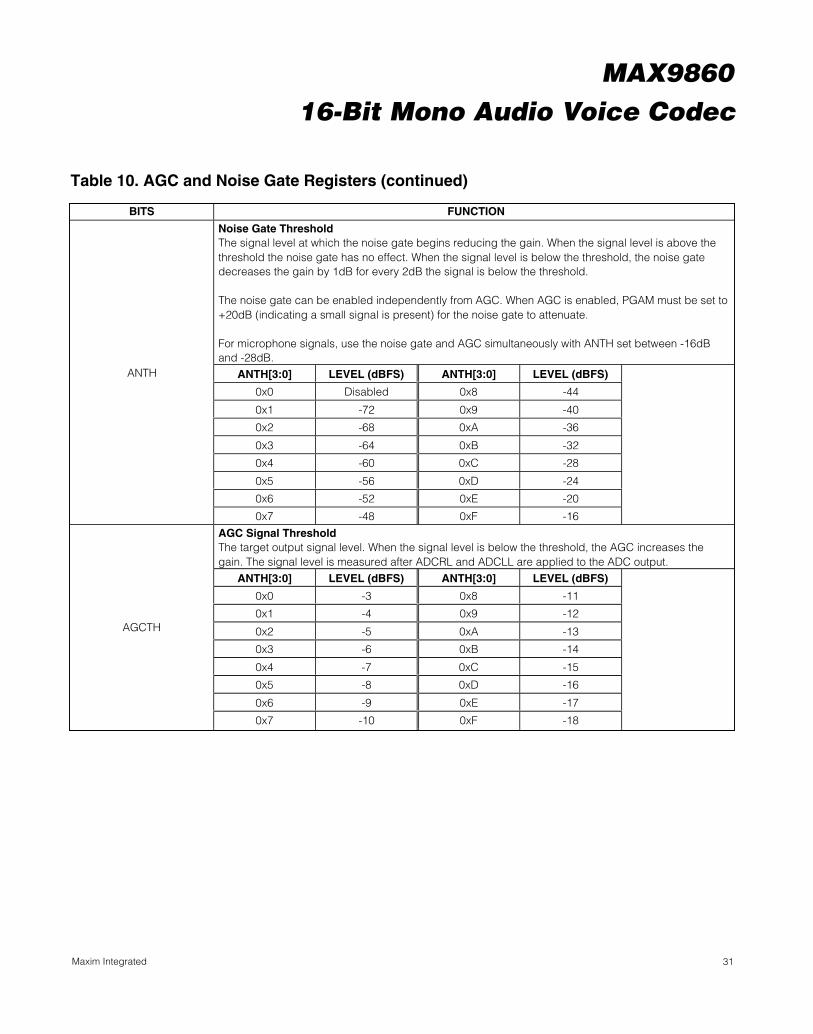
Table 10. AGC and Noise Gate Registers (continued)
BITS FUNCTION
Noise Gate ThresholdThe signal level at which the noise gate begins reducing the gain. When the signal level is above thethreshold the noise gate has no effect. When the signal level is below the threshold, the noise gatedecreases the gain by 1dB for every 2dB the signal is below the threshold.
The noise gate can be enabled independently from AGC. When AGC is enabled, PGAM must be set to+20dB (indicating a small signal is present) for the noise gate to attenuate.
For microphone signals, use the noise gate and AGC simultaneously with ANTH set between -16dBand -28dB.
ANTH[3:0] LEVEL (dBFS) ANTH[3:0] LEVEL (dBFS)
0x0 Disabled 0x8 -44
0x1 -72 0x9 -40
0x2 -68 0xA -36
0x3 -64 0xB -32
0x4 -60 0xC -28
0x5 -56 0xD -24
0x6 -52 0xE -20
ANTH
0x7 -48 0xF -16
AGC Signal ThresholdThe target output signal level. When the signal level is below the threshold, the AGC increases thegain. The signal level is measured after ADCRL and ADCLL are applied to the ADC output.
ANTH[3:0] LEVEL (dBFS) ANTH[3:0] LEVEL (dBFS)
0x0 -3 0x8 -11
0x1 -4 0x9 -12
0x2 -5 0xA -13
0x3 -6 0xB -14
0x4 -7 0xC -15
0x5 -8 0xD -16
0x6 -9 0xE -17
AGCTH
0x7 -10 0xF -18
MAX986016-Bit Mono Audio Voice Codec
32 Maxim Integrated
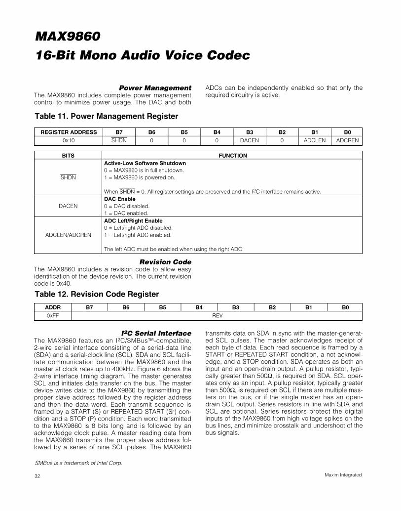
Power ManagementThe MAX9860 includes complete power managementcontrol to minimize power usage. The DAC and both
ADCs can be independently enabled so that only therequired circuitry is active.
Table 11. Power Management Register
REGISTER ADDRESS B7 B6 B5 B4 B3 B2 B1 B00x10 SHDN 0 0 0 DACEN 0 ADCLEN ADCREN
BITS FUNCTION
SHDN
Active-Low Software Shutdown0 = MAX9860 is in full shutdown.1 = MAX9860 is powered on.
When SHDN = 0. All register settings are preserved and the I2C interface remains active.
DACENDAC Enable0 = DAC disabled.1 = DAC enabled.
ADCLEN/ADCREN
ADC Left/Right Enable0 = Left/right ADC disabled.1 = Left/right ADC enabled.
The left ADC must be enabled when using the right ADC.
Revision CodeThe MAX9860 includes a revision code to allow easyidentification of the device revision. The current revisioncode is 0x40.
Table 12. Revision Code Register
ADDR B7 B6 B5 B4 B3 B2 B1 B00xFF REV
I2C Serial InterfaceThe MAX9860 features an I2C/SMBus™-compatible,2-wire serial interface consisting of a serial-data line(SDA) and a serial-clock line (SCL). SDA and SCL facili-tate communication between the MAX9860 and themaster at clock rates up to 400kHz. Figure 6 shows the2-wire interface timing diagram. The master generatesSCL and initiates data transfer on the bus. The masterdevice writes data to the MAX9860 by transmitting theproper slave address followed by the register addressand then the data word. Each transmit sequence isframed by a START (S) or REPEATED START (Sr) con-dition and a STOP (P) condition. Each word transmittedto the MAX9860 is 8 bits long and is followed by anacknowledge clock pulse. A master reading data fromthe MAX9860 transmits the proper slave address fol-lowed by a series of nine SCL pulses. The MAX9860
transmits data on SDA in sync with the master-generat-ed SCL pulses. The master acknowledges receipt ofeach byte of data. Each read sequence is framed by aSTART or REPEATED START condition, a not acknowl-edge, and a STOP condition. SDA operates as both aninput and an open-drain output. A pullup resistor, typi-cally greater than 500Ω, is required on SDA. SCL oper-ates only as an input. A pullup resistor, typically greaterthan 500Ω, is required on SCL if there are multiple mas-ters on the bus, or if the single master has an open-drain SCL output. Series resistors in line with SDA andSCL are optional. Series resistors protect the digitalinputs of the MAX9860 from high voltage spikes on thebus lines, and minimize crosstalk and undershoot of thebus signals.
SMBus is a trademark of Intel Corp.

MAX986016-Bit Mono Audio Voice Codec
33Maxim Integrated
Bit TransferOne data bit is transferred during each SCL cycle. Thedata on SDA must remain stable during the high periodof the SCL pulse. Changes in SDA while SCL is highare control signals (see the START and STOPConditions section).
START and STOP ConditionsSDA and SCL idle high when the bus is not in use.A master initiates communication by issuing a START (S)condition. A START condition is a high-to-low transitionon SDA with SCL high. A STOP (P) condition is a low-to-high transition on SDA while SCL is high (Figure 7). ASTART condition from the master signals the beginningof a transmission to the MAX9860. The master terminatestransmission, and frees the bus, by issuing a STOP con-dition. The bus remains active if a REPEATED START(Sr) condition is generated instead of a STOP condition.
Early STOP ConditionsThe MAX9860 recognizes a STOP condition at anypoint during data transmission except if the STOP con-dition occurs in the same high pulse as a START condi-tion. For proper operation, do not send a STOPcondition during the same SCL high pulse as theSTART condition.
Slave AddressThe slave address is defined as the seven most signifi-cant bits (MSBs) followed by the read/write bit. For theMAX9860, the seven most significant bits are 0010000.Setting the read/write bit to 1 (slave address = 0x21)configures the MAX9860 for read mode. Setting theread/write bit to 0 (slave address = 0x20) configuresthe MAX9860 for write mode. The address is the firstbyte of information sent to the MAX9860 after theSTART condition.
AcknowledgeThe acknowledge bit (ACK) is a clocked 9th bit that theMAX9860 uses to handshake receipt each byte of datawhen in write mode (see Figure 8). The MAX9860 pullsdown SDA during the entire master-generated 9th clockpulse if the previous byte is successfully received.Monitoring ACK allows for detection of unsuccessfuldata transfers. An unsuccessful data transfer occurs ifa receiving device is busy or if a system fault hasoccurred. In the event of an unsuccessful data transfer,the bus master retries communication. The master pullsdown SDA during the 9th clock cycle to acknowledgereceipt of data when the MAX9860 is in read mode. Anacknowledge is sent by the master after each read byteto allow data transfer to continue. A not acknowledge issent when the master reads the final byte of data fromthe MAX9860, followed by a STOP condition.
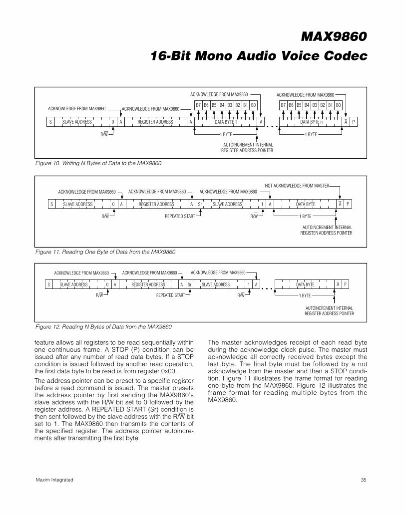
Write Data FormatA write to the MAX9860 includes transmission of aSTART condition, the slave address with the R/W bit setto 0, one byte of data to configure the internal registeraddress pointer, one or more bytes of data, and aSTOP condition. Figure 9 illustrates the proper frameformat for writing one byte of data to the MAX9860.Figure 10 illustrates the frame format for writing n bytesof data to the MAX9860.
The slave address with the R/W bit set to 0 indicatesthat the master intends to write data to the MAX9860.The MAX9860 acknowledges receipt of the addressbyte during the master-generated 9th SCL pulse.
The second byte transmitted from the master config-ures the MAX9860’s internal register address pointer.The pointer tells the MAX9860 where to write the nextbyte of data. An acknowledge pulse is sent by theMAX9860 upon receipt of the address pointer data.
SCL
SDA
tR tF
tBUF
STARTCONDITION
STOPCONDITION
REPEATED START CONDITION START CONDITION
tSU,STO
tHD,STAtSU,STA
tHD,DAT
tSU,DAT tLOW
tHIGH
tHD,STA
tSP
Figure 6. 2-Wire Interface Timing Diagram
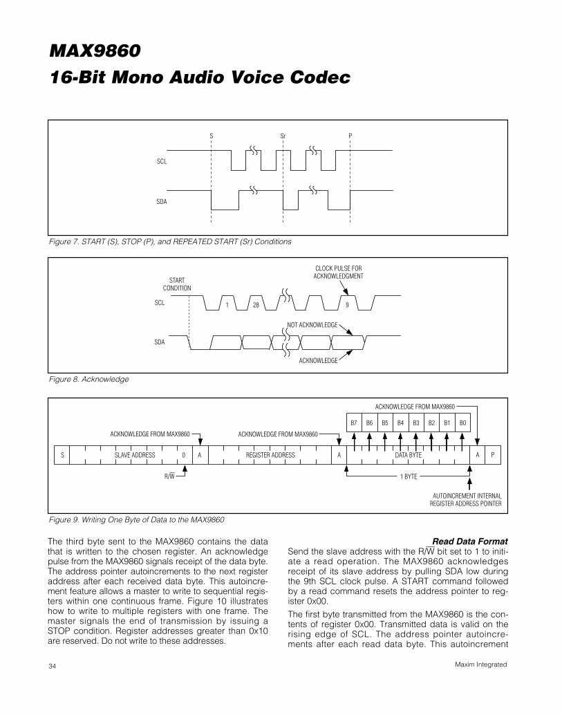
MAX986016-Bit Mono Audio Voice Codec
34 Maxim Integrated
The third byte sent to the MAX9860 contains the datathat is written to the chosen register. An acknowledgepulse from the MAX9860 signals receipt of the data byte.The address pointer autoincrements to the next registeraddress after each received data byte. This autoincre-ment feature allows a master to write to sequential regis-ters within one continuous frame. Figure 10 illustrateshow to write to multiple registers with one frame. Themaster signals the end of transmission by issuing aSTOP condition. Register addresses greater than 0x10are reserved. Do not write to these addresses.
Read Data FormatSend the slave address with the R/W bit set to 1 to initi-ate a read operation. The MAX9860 acknowledgesreceipt of its slave address by pulling SDA low duringthe 9th SCL clock pulse. A START command followedby a read command resets the address pointer to reg-ister 0x00.
The first byte transmitted from the MAX9860 is the con-tents of register 0x00. Transmitted data is valid on therising edge of SCL. The address pointer autoincre-ments after each read data byte. This autoincrement
SCL
SDA
S Sr P
Figure 7. START (S), STOP (P), and REPEATED START (Sr) Conditions
1SCL
STARTCONDITION
SDA
28 9
CLOCK PULSE FORACKNOWLEDGMENT
ACKNOWLEDGE
NOT ACKNOWLEDGE
Figure 8. Acknowledge
A0SLAVE ADDRESS REGISTER ADDRESS DATA BYTE
ACKNOWLEDGE FROM MAX9860
R/W 1 BYTE
AUTOINCREMENT INTERNALREGISTER ADDRESS POINTER
ACKNOWLEDGE FROM MAX9860
ACKNOWLEDGE FROM MAX9860
B1 B0B3 B2B5 B4B7 B6
S AA P
Figure 9. Writing One Byte of Data to the MAX9860
MAX986016-Bit Mono Audio Voice Codec
35Maxim Integrated
feature allows all registers to be read sequentially withinone continuous frame. A STOP (P) condition can beissued after any number of read data bytes. If a STOPcondition is issued followed by another read operation,the first data byte to be read is from register 0x00.
The address pointer can be preset to a specific registerbefore a read command is issued. The master presetsthe address pointer by first sending the MAX9860’sslave address with the R/W bit set to 0 followed by theregister address. A REPEATED START (Sr) condition isthen sent followed by the slave address with the R/W bitset to 1. The MAX9860 then transmits the contents ofthe specified register. The address pointer autoincre-ments after transmitting the first byte.
The master acknowledges receipt of each read byteduring the acknowledge clock pulse. The master mustacknowledge all correctly received bytes except thelast byte. The final byte must be followed by a notacknowledge from the master and then a STOP condi-tion. Figure 11 illustrates the frame format for readingone byte from the MAX9860. Figure 12 illustrates theframe format for reading multiple bytes from theMAX9860.
1 BYTE
AUTOINCREMENT INTERNALREGISTER ADDRESS POINTER
ACKNOWLEDGE FROM MAX9860
ACKNOWLEDGE FROM MAX9860
B1 B0B3 B2B5 B4B7 B6
A A0
ACKNOWLEDGE FROM MAX9860
R/W
S A
1 BYTE
ACKNOWLEDGE FROM MAX9860
B1 B0B3 B2B5 B4B7 B6
PASLAVE ADDRESS REGISTER ADDRESS DATA BYTE 1 DATA BYTE n
Figure 10. Writing N Bytes of Data to the MAX9860
ACKNOWLEDGE FROM MAX9860
1 BYTE
AUTOINCREMENT INTERNALREGISTER ADDRESS POINTER
ACKNOWLEDGE FROM MAX9860NOT ACKNOWLEDGE FROM MASTER
AA PA0
ACKNOWLEDGE FROM MAX9860
R/W
S A
R/WREPEATED START
Sr 1SLAVE ADDRESS REGISTER ADDRESS SLAVE ADDRESS DATA BYTE
Figure 11. Reading One Byte of Data from the MAX9860
ACKNOWLEDGE FROM MAX9860
1 BYTE
AUTOINCREMENT INTERNALREGISTER ADDRESS POINTER
ACKNOWLEDGE FROM MAX9860
AA A P0
ACKNOWLEDGE FROM MAX9860
R/W
S A
R/WREPEATED START
Sr 1SLAVE ADDRESS REGISTER ADDRESS SLAVE ADDRESS DATA BYTE
Figure 12. Reading N Bytes of Data from the MAX9860

MAX986016-Bit Mono Audio Voice Codec
36 Maxim Integrated
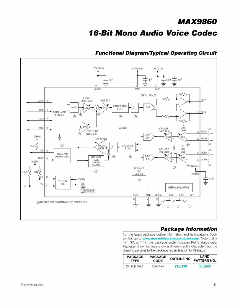
Applications InformationProper layout and grounding are essential for optimumperformance. When designing a PCB for the MAX9860,partition the circuitry so that the analog sections of theMAX9860 are separated from the digital sections. Thisensures that the analog audio traces do not need to berouted near digital traces.
Use a large continuous ground plane on a dedicatedlayer of the PCB to minimize loop areas. ConnectAGND, DGND, and MICGND directly to the groundplane using the shortest trace length possible. Propergrounding improves audio performance, minimizescrosstalk between channels, and prevents any digitalnoise from coupling into the analog audio signal.
Ground the bypass capacitors on REG, PREG, and REFdirectly to the ground plane with minimum trace length.Also be sure to minimize the path length to AGND andMICGND. Bypass AVDD directly to AGND. BypassMICBIAS directly to MICGND.
Connect all digital I/O termination to the ground planewith minimum path length to DGND. Bypass DVDD andDVDDIO directly to DGND.
Route microphone signals from the microphone to theMAX9860 as a differential pair, ensuring that the positiveand negative signals follow the same path as closely aspossible with equal trace length. When using single-ended microphones or other single-ended audiosources, AC ground the negative microphone input sig-nal as near to the audio source as possible and then treatthe positive and negative traces as differential pairs.
The MAX9860 thin QFN package features an exposedthermal pad on its underside. This pad lowers the pack-age’s thermal resistance by providing a direct heatconduction path from the die to the PCB. Connect theexposed thermal pad to AGND.
An evaluation kit (EV kit) is available to provide anexample layout for the MAX9860. The EV kit allowsquick setup of the MAX9860 and includes easy-to-usesoftware allowing all internal registers to be controlled.
2324 22 21
87 9
REG
REF
AGND
AVDD
10
MICBIAS
LRCLK
SDOUT
MCLK
BCLK
DVDD
1
2
MIC
LN
4
5
6
17
18
16
14
13
MIC
LP
MIC
GND
SCL
SDA
OUTN
OUTP
MAX9860
PREG SDIN3
15
MIC
RP20
11
DVDD
IOM
ICRN
19
12
DGND
IRQ
THIN QFN4mm x 4mm
TOP VIEW
*EP
*EP = EXPOSED PAD
+
Pin Configuration
MAX986016-Bit Mono Audio Voice Codec
37Maxim Integrated
PP
PP
PP
P
P
PPP
P
P
P
P
P P
P
0 TO +20dB(1dB STEPS)
DAC
DVDDIO
IRQ
14MCLK
10SCL
9SDA
AGND
5
I2C SERIALPORT
23
22
0,20dB,30dB
21
20
0,20dB,30dB
LEFTADC
RIGHTADC
INTERPOLATIONFILTER
DECIMATIONFILTER
INTERNAL REGULATORS
REG2
PREG3
REF4
DIGITAL AUDIOINTERFACE
17LRCLK
18BCLK
16SDIN
15SDOUT
MONO
LOW-LEVELAUDIO
QUIETINGCONTROL
AUTOMATICGAIN
CONTROL
TIMING ANDCONTROL LOGIC
6
AVDD
1.7V TO 1.9V 1.7V TO 1.9V
STATUS
USER-PROGRAMMABLEMODE CONTROL
DGND
12
DIGITAL ANALOG
MICLP
MICLN
MICRP
MICRN
0 TO +20dB(1dB STEPS)
MICBIAS
MICBIAS
1
24
MICGND
7
8
OUTP
OUTN
INDICATES USER PROGRAMMABLE I2C CONTROL BITS.
0, +6dB,+12dB, +24dB -90dB TO 0
-60dB TO 0dB(2dB STEPS)
-12dB TO +3dB
11
DVDDIO DVDD13
1.7V TO 3.6V
DVDDIO
19
DVG DVA
DVST
PAMPGAM
PAMPGAM
ADCLL/ADCRL
10kΩ
1.5kΩ 1.5kΩ
10µF0.1µF1µF
1µF
1µF
1µF
1µF
2.2µF
1µF 1µF 2.2µF
1µF
P
MAX9860
Σ
Functional Diagram/Typical Operating Circuit
Package InformationFor the latest package outline information and land patterns (foot-prints), go to www.maximintegrated.com/packages. Note that a“+”, “#”, or “-” in the package code indicates RoHS status only.Package drawings may show a different suffix character, but thedrawing pertains to the package regardless of RoHS status.
PACKAGETYPE
PACKAGECODE
OUTLINE NO.LAND
PATTERN NO.
24 TQFN-EP T2444+4 21-0139 90-0022

Maxim Integrated cannot assume responsibility for use of any circuitry other than circuitry entirely embodied in a Maxim Integrated product. No circuit patentlicenses are implied. Maxim Integrated reserves the right to change the circuitry and specifications without notice at any time. The parametric values (min andmax limits) shown in the Electrical Characteristics table are guaranteed. Other parametric values quoted in this data sheet are provided for guidance.
38 ________________________________Maxim Integrated 160 Rio Robles, San Jose, CA 95134 USA 1-408-601-1000
© 2012 Maxim Integrated Products, Inc. Maxim Integrated and the Maxim Integrated logo are trademarks of Maxim Integrated Products, Inc.
MAX986016-Bit Mono Audio Voice Codec
Revision History
REVISIONNUMBER
REVISIONDATE
DESCRIPTIONPAGES
CHANGED
0 10/08 Initial release —
1 9/09 Corrected error in Table 11 32
2 2/12 Removed VOS typical spec and updated max spec 5