Embed Size (px)
Citation preview
Linköping Studies in Science and Technology
Dissertation, No. 1467
Synthesis of ZnO, CuO and their Composite Nanostructures
for Optoelectronics, Sensing and Catalytic Applications
Saima Zaman
Physical Electronics and Nanotechnology
Department of Science and Technology
Linköping University, SE-601 74 Norrköping Sweden
Synthesis of ZnO, CuO and their Composite Nanostructures
for Optoelectronics, Sensing and Catalytic Applications
Saima Zaman
ISBN: 978-91-7519-818-7
ISSN: 0345-7524
Copyright©, 2012, Saima Zaman
Linköping University
Department of Science and Technology
SE- 60174 Norrköping
Sweden
Printed by LiU-Tryck, Linköping 2012

Dedicated to:
My Father and Mother

Abstract
i
Abstract
Research on nanomaterials has become increasingly popular because of their
unique physical, chemical, optical and catalytic properties compared to their bulk
counterparts. Therefore, many efforts have been made to synthesize
multidimensional nanostructures for new and efficient nanodevices. Among those
materials, zinc oxide (ZnO), has gained substantial attention owing to many
outstanding properties. ZnO besides its wide bandgap of 3.34 eV exhibits a
relatively large exciton binding energy (60 meV) at room temperature which is
attractive for optoelectronic applications. Likewise, cupric oxide (CuO), having a
narrow band gap of 1.2 eV and a variety of chemo-physical properties that are
attractive in many fields. Moreover, composite nanostructures of these two oxides
(CuO/ZnO) may pave the way for various new applications.
This thesis can be divided into three parts concerning the synthesis,
characterization and applications of ZnO, CuO and their composite nanostructures.
In the first part the synthesis, characterization and the fabrication of ZnO
nanorods based hybrid light emitting diodes (LEDs) are discussed. The low
temperature chemical growth method was used to synthesize ZnO nanorods on
different substrates, specifically on flexible non-crystalline substrates. Hybrid LEDs
based on ZnO nanorods combined with p-type polymers were fabricated at low
temperature to examine the advantage of both materials. A single and blended light
emissive polymers layer was studied for controlling the quality of the emitted white
light.
The second part deals with the synthesis of CuO nanostructures (NSs) which
were then used to fabricate pH sensors and exploit these NSs as a catalyst for
degradation of organic dyes. The fabricated pH sensor exhibited a linear response
and good potential stability. Furthermore, the catalytic properties of petals and
Abstract
ii
flowers like CuO NSs in the degradation of organic dyes were studied. The results
showed that the catalytic reactivity of the CuO is strongly depending on its shape.
In the third part, an attempt to combine the advantages of both ZnO and CuO
NSs was performed by developing a two-step chemical growth method to
synthesize the composite NSs. The synthesized CuO/ZnO composite NSs revealed
an extended light absorption and enhanced defect related visible emission.
Keywords: Zinc Oxide, Copper (II) oxide, Nanostructures, Low temperature
Growth, Light emitting diodes, pH sensor

Acknowledgement
iii
Acknowledgement
This thesis is the end of my journey in obtaining my Ph.D degree. I have not traveled
alone in this journey. This thesis has been kept on track and been seen through to
completion with the support and encouragement of numerous people. At the end I
would like to thank all those people who made this thesis possible and an
unforgettable experience to me. Truly, words are not enough to express my
gratitude to all of them.
First and foremost, I would like to express my overwhelming gratitude to my
supervisor, Prof. Magnus Willander, for giving me the chance to work in his
research group. Thanks for giving me freedom for developing my research ideas, for
showing me different ways to approach a research problem and the need to be
persistent to accomplish any goal and for always being there whenever I need your
help.
I render to pay special thanks to my co-supervisor, associate Prof. Omer Nour for
his keen interest, encouragement and for his support throughout this work.
I owe my sincere thanks to all my co-authors of the included papers, especially
Ahmed Zainelabdin for his extensive discussions and valuable support during this
work.
I would like to thank our research administrator Ann-Christin Norén for her kind
administrative help and cooperation.
I greatly acknowledge the facilities and financial support provided by the ITN/
Linköping University and MUST University AJK Pakistan throughout my Ph.D.
studies.

Acknowledgement
iv
I offer my sincere wishes and thanks to all present and previous members of the
Physical Electronics and Nanotechnology group for their cooperation and moral
support.
My deepest debt of gratitude is to my entire family for their love and support. I
must appreciate my brothers, my sisters and all my in-laws family for their guidance
and encouragement. Most importantly, my father and mother, it was your dream
which made my journey up to this possible. All I can say is, this small space is not
enough to acknowledge your contributions up to this stage of my life. May Allah
bless you all!!!
At the last but not the least, most special thanks I accord to my husband, Faisal for
his unwavering understanding and support during all these years of my Ph.D. He
was always there cheering me up and stood by me through the good and bad times.
Without you nothing of this would have been possible. Thanks for being with me. I
appreciate my beloved kids Musa and Zoha, who have provided me all the joy of
life with their innocent acts and refreshing me with lovely smiles.
List of Publications
v
List of Publications
Papers included in this thesis
I. Deposition of well-aligned ZnO nanorods at 50oC on metal,
semiconducting polymer, and copper oxides substrates and their structural
and optical Properties
A. Zainelabdin, S. Zaman, G. Amin, O. Nur, and M. Willander.
Crystal Growth & Design, 10, 3250 (2010).
II. ZnO nanorods–polymer hybrid white light emitting diode grown on a
disposable paper substrate
G. Amin, S. Zaman, A. Zainelabdin, O. Nur, and M. Willander
Physics Status Solidi RRL 5, 71 (2011).
III. Influence of the polymer concentration on the electroluminescence of ZnO
nanorods/polymer hybrid light emitting diode
S. Zaman, A. Zainelabdin, G. Amin, O. Nur, and M. Willander
Accepted in Journal of Applied Physics (2012).
IV. Effect of the polymer emission on the electroluminescence characteristics
of ZnO nanorods/p-polymer hybrid light emitting diode
S. Zaman, A. Zainelabdin, G. Amin, O. Nur, and M. Willander
Applied Physics A, 104, 1203 (2011).
V. CuO nanoflowers as an electrochemical pH sensor and the effect of the pH
on the growth
S. Zaman, M. H. Asif, A. Zainelabadin, G. Amin, O. Nur, and M. Willander
Journal of Electroanalytical Chemistry 662, 421 (2011).
VI. Efficient catalytic effect of two-dimensional petals and three-dimensional
flowers like CuO nanostructures on the degradation of organic dyes
List of Publications
vi
S. Zaman, A. Zainelabadin, G. Amin, O. Nur and M. Willander
Journal of Physics and Chemistry of Solids 73, 1320 (2012).
VII. Synthesis and characterization of CuO/ZnO composite nanostructures:
precursor’s effects, and their optical properties
A. Zainelabdin, S. Zaman, S. Hussain, O. Nur, and M. Willander
Submitted (2012).
Related papers not included in this thesis
1. Different interfaces to crystalline ZnO nanorods and their applications
M. Willander, M. H. Asif, S. Zaman, A. Zainelabdin, N. Bano, S. M. Al-Hilli,
and O. Nur
Phys. Status Solidi C 6, 2683 (2009).
2. Low-temperature chemical growth of ZnO nanorods with enhanced UV
emission on plastic substrates
S. Zaman, A. Zainelabdin, G. Amin, O. Nur, and M. Willander
Journal of Nanoelectronics & Optoelectronics, 5, 1, (2010).
3. Stable white light electroluminescence from highly flexible polymer/ZnO
nanorods hybrid heterojunction grown at 50oC
A. Zainelabdin, S. Zaman, G. Amin, O. Nur, and M. Willander
Nanoscale Research Letter, 5, 1442 (2010).
4. ZnO-organic hybrid white light emitting diodes grown on flexible plastic
using low temperature aqueous chemical method
N. Bano, S. Zaman, A. Zainelabdin, S. Hussain, I. Hussain, O. Nur, and M.
Willander
Journal of Applied Physics 108, 043103 (2010).
List of Publications
vii
5. Current-transport studies and trap extraction of hydrothermally grown
ZnO nanotubes using gold Schottky diode
G. Amin, I. Hussain, S. Zaman, N. Bano, O. Nur and Magnus Willander
Physics Status Solidi A, 207, 748 (2010).
6. Luminescence from zinc oxide nanostructures and polymers and their
Hybrid Devices
M. Willander, O. Nur, J. R. Sadaf, M. Q. Israr, S. Zaman, A. Zainelabdin, N.
Bano and I. Hussain
Materials 3, 2643 (2010)
7. Influence of pH, precursor concentration, growth time, and temperature on
the morphology of ZnO nanostructures grown by the hydrothermal method
G. Amin, M. H. Asif, A. Zainelabdin, S. Zaman, O. Nur, and M. Willander
Journal of Nanomaterials doi:10.1155/2011/269692 (2011)
8. Zinc Oxide nanorods/polymer hybrid heterojunctions for white light
emitting diodes
M. Willander, O. Nur, S. Zaman, A. Zainelabdin, N. Bano, and I. Hussain
J. Phys. D: Appl. Phys. 44, 224017 (2011).
9. Intrinsic white light emission from zinc oxide nanorods heterojunctions on
large area substrates
M. Willander, O. Nur , S. Zaman, A. Zainelabdin, G. Amin, J. R. Sadaf, M. Q.
Israr, N. Bano, I. Hussain, and N. H. Alvi
Proceedings of SPIE 7940, 79400A (2011)
10. Zinc Oxide and copper oxide nanostructures: fundamentals and
applications
Magnus Willander, Omer Nur, Gul Amin, A. Zainelabdin and S. Zaman
MRS Fall Meeting 2011.
List of Publications
viii
11. Scale-up synthesis of ZnO nanorods for printing inexpensive ZnO/Polymer
white light emitting diode
G. Amin, M. O. Sandberg, A. Zainelabdin, S. Zaman, O. Nur, and M.
Willander
Journal of Materials Science 47, 4726 (2012).
12. Optical and current transport properties of CuO/ZnO nanocorals p-n
heterostructure hydrothermally synthesized at low temperatures.
A. Zainelabdin, S. Zaman, G. Amin, O. Nur, and M. Willander
Applied Physics A, 108, 921 (2012)
13. CuO/ZnO Nanocorals synthesis via hydrothermal technique: growth
mechanism and their application as Humidity Sensor
A. Zainelabdin, G. Amin, S. Zaman, O. Nur, J. Lu, L. Hultman, and M.
Willander
Journal of Material Chemistry 22, 11583 (2012)
14. CuO nanopetals based electrochemical sensor for selective Ag+
measurements
G. Amin, M. H. Asif, A. Zainelabdin, S. Zaman, O. Nur, and M. Willander
Sensor Letters 10, 1 (2012).
15. Recent progress on growth and device development of ZnO and CuO
nanostructures and graphene nanosheets
M. Willander, K. ul Hassan, O. Nur, A. Zainelabdin, S. Zaman and G. Amin
Journal of Materials Chemistry 22, 2337 (2012)
16. Metal Oxide nanostructures and white light emission
A. Zainelabdin, O. Nur, G. Amin, S. Zaman, and M. Willander
Proceedings of SPIE 8263, 82630N (2012)
List of Publications
ix
17. CuO Interpenetrated leaves architecture originated from (101) Twin
Structure
J. Lu, A. Zainelabdin, S. Zaman, G. Amin, O. Nur, M. Willander and L.
Hultman
Submitted
Co
Contribution to the papers included in the thesis
Contribution to the paper I, II & VII
Part of the experimental work and involved in the editing of the manuscripts.
Contribution to paper III, IV, V, VI
Design and performance of the experiments except the TEM and PL measurements,
data analysis and wrote the first version of the manuscript.

Table of Contents
xi
Table of Contents
Abstract ......................................................................................................................................... i
Acknowledgement ................................................................................................................... iii
List of Publications ....................................................................................................................v
Introduction ................................................................................................................................. 1
1.1 Background ........................................................................................................................ 1
1.2 Objective and outline of this thesis ............................................................................... 3
Materials and properties........................................................................................................... 5
2.1 Zinc Oxide .......................................................................................................................... 5
2.2 Copper (II) Oxide .............................................................................................................. 8
2.3 Polymers ............................................................................................................................. 9
2.3.1 Poly(9,9-dioctylfluorene) (PFO) ............................................................................ 10
2.3.2 MEH-PPV .................................................................................................................. 12
Synthesis and characterization of nanomaterials ............................................................ 13
3.1 Synthesis of ZnO ............................................................................................................. 13
3.1.1 Chemical bath deposition growth of ZnO NRs................................................. 14
3.1.2 Characterization of ZnO NRs ................................................................................ 15
3.2 Synthesis of CuO nanostructures ................................................................................ 17
3.2.1. Characterization of CuO nanostructures ........................................................... 18
3.3 Synthesis of CuO/ZnO composite nanostructure ................................................... 21
3.3.1 Characterization of CuO/ZnO composite nanostructure............................... 22
Fabrication and characterization of devices ...................................................................... 27
Table of Contents
xii
4.1 ZnO NRs/polymers hybrid LEDs .............................................................................. 27
4.1.1 Characterization of hybrid LEDs on disposable paper substrates ............... 31
4.1.2 Influence of the polymer concentration on hybrid LEDs ............................... 32
4.1.3 Effect of the polymer emission on the EL of hybrid LEDs ............................. 35
4.2. CuO based electrochemical pH sensor ..................................................................... 39
4.2.1. Characterization of CuO pH sensors ................................................................. 41
4.3. CuO nanostructures as a catalyst ............................................................................... 43
4.3.1 Catalytic performance of CuO nanostructures ................................................. 44
Conclusion and future work ................................................................................................. 47
References .................................................................................................................................. 49
Introduction
1
Chapter 1
Introduction
The little word "nano" with huge potential has been rapidly indicating itself into the world's
map and has an enormous influence in every aspect of science and engineering fields. The
idea of nanotechnology was introduced by Richard Feynman in his talk “There is a plenty of
room at the bottom”, in 1959. Though he never explicitly mentioned "nanotechnology,"
Feynman suggested that it will eventually be possible to precisely manipulate atoms and
molecules. In general, nanotechnology consists of materials with nanoscale dimensions,
remarkable properties, and great potential.
1.1 Background During the last few decades, nanomaterials have been the subject of extensive
interest because of their potential use in a wide range of fields like, optoelectronics,
catalysis and sensing applications etc. The physical and chemical properties of
nanomaterials can differ significantly from their bulk counterpart because of their
small size. In general, nanomaterials comprised novel properties that are typically
not observed in their conventional, bulk counterparts. Nanomaterials have a much
larger surface area to volume ratio than their bulk counterparts, which is one of the
basis of their novel physical and/or chemical properties. Nanomaterials are
classified into one-dimensional (1D), two-dimensional (2D) and three-dimensional
(3D). At present, research on nanomaterials is intensified and is expanding rapidly.
In addition, metal oxide nanomaterials have drawn a particular attention because of
their excellent structural flexibility combined with other attractive properties. These
metal oxides nanostructures not only inherit the fascinating properties from their
bulk form such as piezoelectricity, chemical sensing, and photodetection, but also
possess unique properties associated with their highly anisotropic geometry and
Introduction
2
size confinement [1]. The combinations of the new and the conventional properties
with the unique effects of nanostructures make the investigation of novel metal
oxide nanostructures a very important issue in research and development both from
fundamental and industrial standpoints.
Among the various metal oxides, zinc oxide (ZnO) possessed a considerable
attention due to its unique properties and applications. In particular, ZnO
nanostructures (NSs) are of intense interest since they can be grown by a variety of
methods with different morphologies. Among the different growth methods, the
chemical bath deposition method is low temperature, simple, inexpensive and
environment friendly method. These are all factors which further contribute to the
resurgent attention in ZnO. Specifically, one-dimensional ZnO nanorods (NRs)
amongst other nanostructures are attractive components for manufacturing
nanoscale electronics and photonic devices as well as their biomedical applications
because of their interesting chemical and physical properties [2, 3]. Also ZnO NRs
can easily be grown on a variety of substrates like metal surface, semiconductors,
glass, plastic and disposable paper substrates etc. [4-7]. Furthermore, a direct wide
band gap ~ 3.37 eV and relatively large excitonic binding energy ~ 60 meV of ZnO
along with many radiative deep level defects, makes ZnO attractive for its emission
tendency in blue/ultraviolet and full colour lighting [8, 9]. To utilize theses
properties of ZnO in LEDs application, another p-type material is necessary as ZnO
NRs is unintentionally n-type material. Since mostly polymers are p-type and their
special properties like low cost, low power consumption, flexible and easy
manufacturing all makes polymers a better choice to use with ZnO NRs to fabricate
a flexible device that utilizes the properties of both materials for large area lighting
and display application [10, 11].
On the other hand, natural abundance of copper (II) oxide (CuO) as well as its
low production cost, good electrochemical and catalytic properties makes the copper
Introduction
3
oxide to be one of the best materials for various applications. CuO also has a variety
of nanostructures and can be grown using the low temperature aqueous chemical
method. It is one of the most important catalysts and is widely used in
environmental catalyst.
1.2 Objective and outline of this thesis
The objective of this thesis is to synthesize metal oxide semiconductor
nanostructures and utilize them for light emitting diodes, catalytic and sensing
applications. For the ease of gathering all presented work, the thesis is divided into
parts:
i) Synthesis of ZnO and CuO nanostructures. The morphology, crystal structure
and crystallinity of the nanostructures were monitored by using scanning electron
microscope (SEM), transmission electron microscope (TEM) and x-ray diffraction.
ii) Fabrication of a solution-processable hybrid ZnO NRs/polymer light emitting
diodes (LEDs) on flexible substrates. N-type ZnO NRs grown along the c-axis direction
act as natural waveguide cavities for making the emitted light to travel to the top of
the devices. Along with the properties of the ZnO NRs, choice of the polymer is also
crucial for tuning the emission of fabricated LEDs. The emission colour of the hybrid
LEDs can be tuned by blending different polymers or by changing the polymer
concentrations.
iii) Utilization of the CuO nanostructures to develop a pH sensor and exploit these
NSs as a catalyst to degrade organic dyes. Owing to its good electrochemical activity,
CuO is a promising candidate for sensing applications. Thus, CuO based pH sensor
was developed to check the sensitivity and response over a wide pH range.
Moreover, CuO is known to be a good catalyst and morphology of the CuO affects
the properties of the catalyst in general. Therefore CuO NSs having different
morphology were investigated to boost the degradation of the organic dyes.
Introduction
4
iv) Finally, extend the growth of ZnO and CuO to achieve their composite CuO/ZnO
nanostructure. The growth kinetics of composite NSs was studied and found that it
depends on the nature and the pH value of the nutrient solution. The CuO/ZnO
nanocomposite exhibited a broad and extended light absorption covering the whole
visible range.
The outline of this thesis is as follow: the general introduction and the
objective of the thesis are presented in this chapter. Some basic properties of ZnO,
CuO and polymers are studied in the following chapter. The synthesis of CuO, ZnO
and their composite nanostructures together with characterization is the subject of
chapter 3. Their applications in hybrid ZnO NRs/polymer LED, pH sensor based on
CuO and catalytic effect of the CuO NSs were demonstrated in the chapter 4. The
final chapter contains the conclusion of whole work and possible future prospects.
Materials and properties
5
Chapter 2
Materials and properties
ZnO is a wide bandgap material possessing many interesting properties and probably the
richest family of nanostructures. Moreover, CuO is a narrow bandgap material and has been
studied extensively. In this chapter we aim to narrate some properties of ZnO and CuO in a
comprehensive manner, as well as discuss the polymers which are used in this work.
2.1 Zinc Oxide
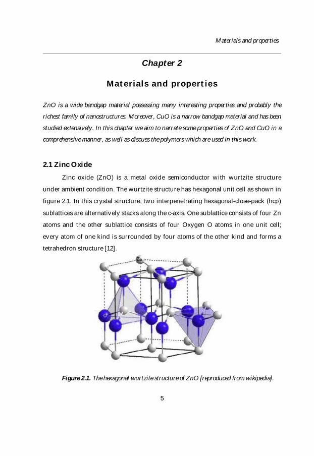
Zinc oxide (ZnO) is a metal oxide semiconductor with wurtzite structure
under ambient condition. The wurtzite structure has hexagonal unit cell as shown in
figure 2.1. In this crystal structure, two interpenetrating hexagonal-close-pack (hcp)
sublattices are alternatively stacks along the c-axis. One sublattice consists of four Zn
atoms and the other sublattice consists of four Oxygen O atoms in one unit cell;
every atom of one kind is surrounded by four atoms of the other kind and forms a
tetrahedron structure [12].
Figure 2.1. The hexagonal wurtzite structure of ZnO [reproduced from wikipedia].
Materials and properties
6
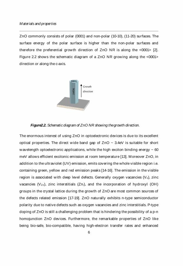
ZnO commonly consists of polar (0001) and non-polar (10-10), (11-20) surfaces. The
surface energy of the polar surface is higher than the non-polar surfaces and
therefore the preferential growth direction of ZnO NR is along the <0001> [2].
Figure 2.2 shows the schematic diagram of a ZnO NR growing along the <0001>
direction or along the c-axis.
Figure2.2. Schematic diagram of ZnO NR showing the growth direction.
The enormous interest of using ZnO in optoelectronic devices is due to its excellent
optical properties. The direct wide band gap of ZnO ~ 3.4eV is suitable for short
wavelength optoelectronic applications, while the high exciton binding energy ~ 60
meV allows efficient excitonic emission at room temperature [13]. Moreover ZnO, in
addition to the ultraviolet (UV) emission, emits covering the whole visible region i.e.
containing green, yellow and red emission peaks [14-16]. The emission in the visible
region is associated with deep level defects. Generally oxygen vacancies (Vo), zinc
vacancies (VZn), zinc interstitials (Zni), and the incorporation of hydroxyl (OH)
groups in the crystal lattice during the growth of ZnO are most common sources of
the defects related emission [17-19]. ZnO naturally exhibits n-type semiconductor
polarity due to native defects such as oxygen vacancies and zinc interstitials. P-type
doping of ZnO is still a challenging problem that is hindering the possibility of a p-n
homojunction ZnO devices. Furthermore, the remarkable properties of ZnO like
being bio-safe, bio-compatible, having high-electron transfer rates and enhanced
Growth
direction
(0001)
(ퟏퟎퟏퟎ)
Materials and properties
7
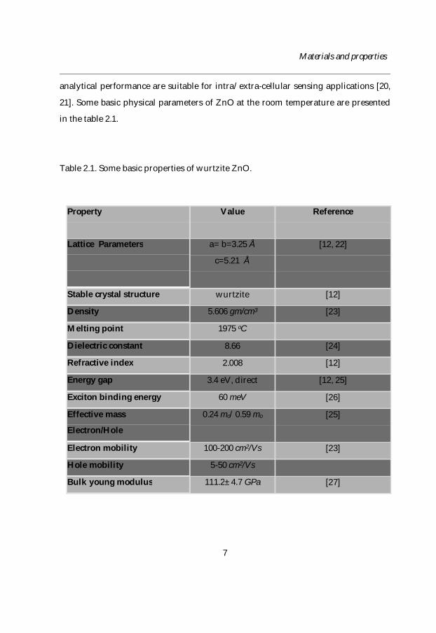
analytical performance are suitable for intra/extra-cellular sensing applications [20,
21]. Some basic physical parameters of ZnO at the room temperature are presented
in the table 2.1.
Table 2.1. Some basic properties of wurtzite ZnO.
Property
Value
Reference
Lattice Parameters
a= b=3.25 Å
c=5.21 Å
[12, 22]
Stable crystal structure wurtzite [12]
Density 5.606 gm/cm3 [23]
Melting point 1975 oC
Dielectric constant 8.66 [24]
Refractive index 2.008 [12]
Energy gap 3.4 eV, direct [12, 25]
Exciton binding energy 60 meV [26]
Effective mass
Electron/Hole
0.24 mo/0.59 mo
[25]
Electron mobility 100-200 cm2/Vs [23]
Hole mobility 5-50 cm2/Vs
Bulk young modulus 111.2±4.7 GPa [27]
Materials and properties
8
2.2 Copper (II) Oxide
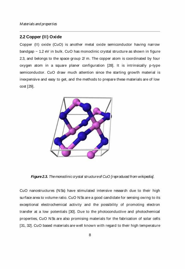
Copper (II) oxide (CuO) is another metal oxide semiconductor having narrow
bandgap ~ 1.2 eV in bulk. CuO has monoclinic crystal structure as shown in figure
2.3, and belongs to the space group 2/m. The copper atom is coordinated by four
oxygen atom in a square planer configuration [28]. It is intrinsically p-type
semiconductor. CuO draw much attention since the starting growth material is
inexpensive and easy to get, and the methods to prepare these materials are of low
cost [29].
Figure 2.3. The monoclinic crystal structure of CuO [reproduced from wikipedia].
CuO nanostructures (NSs) have stimulated intensive research due to their high
surface area to volume ratio. CuO NSs are a good candidate for sensing owing to its
exceptional electrochemical activity and the possibility of promoting electron
transfer at a low potentials [30]. Due to the photoconductive and photochemical
properties, CuO NSs are also promising materials for the fabrication of solar cells
[31, 32]. CuO based materials are well known with regard to their high temperature
Materials and properties
9
superconductivity and the relatively huge magnetoresistance [33, 34]. Additionally,
this compound is well-known for its excellent performance as a sensing material for
hazardous gas detection and as negative electrode in lithium ions batteries [35-37].
CuO is very important from the standpoint of the catalytic usage and the
morphology affects the properties of a catalyst in general [38]. It is therefore
significant to synthesize novel sizes and shapes of the CuO NSs and to further
improve its application as a catalyst. Some of the physical features of CuO are
summarized in table 2.2.
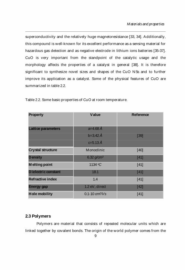
Table 2.2. Some basic properties of CuO at room temperature.
2.3 Polymers Polymers are material that consists of repeated molecular units which are
linked together by covalent bonds. The origin of the world polymer comes from the
Property
Value
Reference
Lattice parameters
a=4.68 Å
b=3.42 Å
c=5.13 Å
[39]
Crystal structure Monoclinic [40]
Density 6.32 g/cm3 [41]
Melting point 1134 oC [41]
Dielectric constant 18.1 [41]
Refractive index 1.4 [41]
Energy gap 1.2 eV, direct [42]
Hole mobility 0.1-10 cm2/Vs [41]
Materials and properties
10
Greek language where poly means ´many´ and mer means ´part´. Conjugated
polymers are novel materials that combine the optoelectronic properties of
semiconductors with the mechanical properties and processing advantage of the
plastics. The conjugated polymers are organic macromolecules which consist at least
of one backbone chain of alternating single and double bonds [43]. It is the π
electrons, which mainly determine the electronic and optical properties of the
molecule. In ground state, the π-electrons form the π-band and the highest energy π-
electron level is known as the highest occupied molecular orbital (HOMO). In
excited state, the π-electrons form the π*-band and the lowest energy π*-electron
level is known as the lowest unoccupied molecular orbital (LUMO). The HOMO
resembles the valence band and the LUMO resembles the conduction band in the
inorganic semiconductor concepts [44].
In this work two light emitting polymers were chosen for the
fabrication of the hybrid LEDs.
2.3.1 Poly(9,9-dioctylfluorene) (PFO)
Poly(9,9-dioctylfluorene) (PFO) is the most promising candidate as a blue-
light-emitting polymer because of its highly efficient photoluminescence, good
thermal, chemical stability at elevated temperatures and solubility in organic
solvents. The HOMO and LUMO energy levels of the PFO are in the range of 5.6 eV
– 5.8 eV and 2.12 eV – 2.6 eV, respectively giving ~ 3.2 eV energy bandgap,
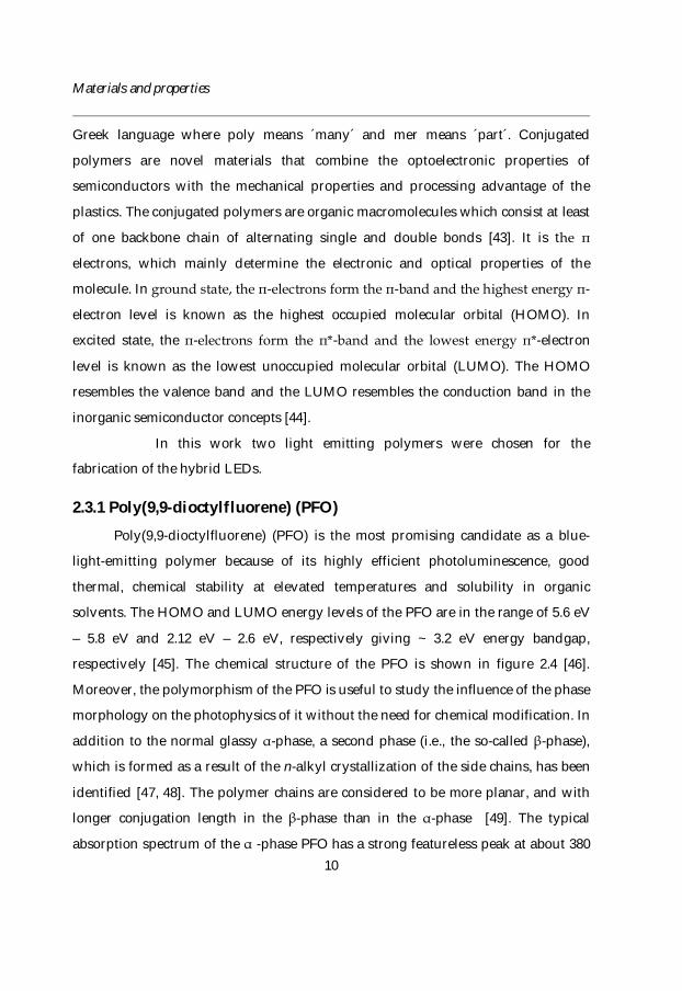
respectively [45]. The chemical structure of the PFO is shown in figure 2.4 [46].
Moreover, the polymorphism of the PFO is useful to study the influence of the phase
morphology on the photophysics of it without the need for chemical modification. In
addition to the normal glassy α-phase, a second phase (i.e., the so-called β-phase),
which is formed as a result of the n-alkyl crystallization of the side chains, has been
identified [47, 48]. The polymer chains are considered to be more planar, and with
longer conjugation length in the β-phase than in the α-phase [49]. The typical
absorption spectrum of the α -phase PFO has a strong featureless peak at about 380
Materials and properties
11
nm whereas the β-phase has demonstrated a narrow, well-resolved absorption peak
at 437 nm [50]. These α and β-phases have a number of interesting photophysical
properties and have been investigated as systems well suited to the detailed study of
energy transfer processes [51-53]
Figure 2.4. The chemical structure of the PFO.
Aside from the morphology-induced changes (i.e. β-phase formation), the
observation of the distinct photophysical changes due to photo- and/or electro
degradation processes is of significant importance for device fabrication. The
polyfluorene based devices suffer from a degradation of the device under operation,
which is most visible in the formation of a low energy emission band (green
emission) [54]. This degradation behavior turns the blue emission color of PFO into
blue-green emission. The source of this green emission band is a matter of
controversy. This low energy emission band is associated with the fluorenone
defects (or ketone defects) in the form of fluorenone moieties in the polymer
backbone [55, 56]. Such fluorenone defects, leading to the low energy emission band
in polyfluorene, and can be formed during synthesis, or as a result of a photo-(or
electro)-oxidation degradation processes [57].
Materials and properties
12
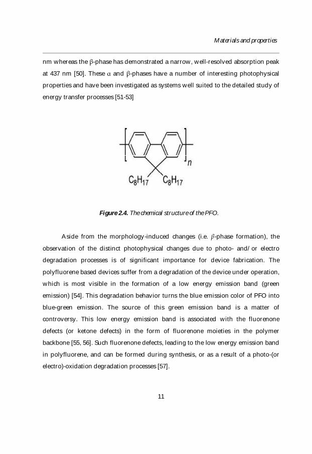
2.3.2 MEH-PPV Poly[2-methoxy-5-(2-ethylhexyloxy)-1,4-phenylenevinylene] (MEH-PPV) is
one of the most widely investigated light-emitting polymers within the class of
PPVs. The MEH-PPV has a small energy bandgap of about 2.1 eV as estimated from
the HUMO-LUMO energy difference [58, 59]. Therefore, it is well-known that this
polymer shows orange-red emission when it is processed into electroluminescence
devices. It can easily be dissolved in many organic solvents which allow the MEH-
PPV to be easily processed for thin films [60]. The chemical structure of the MEH-
PPV is shown in figure 2.5 [61]
Figure 2.5. The chemical structure of MEH-PPV.
Synthesis and characterization of nanomaterials
13
Chapter 3
Synthesis and characterization of nanomaterials
The growth procedure of the ZnO and CuO nanostructures are described in this chapter. The
low temperature chemical bath deposition method was chosen for the growth of ZnO, CuO
and their composite nanostructures. After the growth, diverse characterization techniques
were used to probe the morphology and structural aspects of the as grown nanomaterials. The
techniques used during this work are: scanning electron microscope (SEM), transmission
electron microscope (TEM) and x-ray diffraction analysis. The working principles of these
techniques are appended in [62-64].
3.1 Synthesis of ZnO
In recent years, with the increasing awareness of both environmental safety
and the need for optimal energy utilization, there is a case for the development of
nonhazardous materials. These materials should not only be compatible with human
life but also with other living forms or species. Moreover, processing methods such
as fabrication, manipulation, treatment, reuse, and recycling of waste materials
should be environmentally friendly. In this respect, the hydrothermal technique
occupies a unique place in modern science and technology.
The hydrothermal growth technique is promising for low cost and for scaling
up the synthesis of nanostructures. This technique is not only useful to grow single
material but can also be useful to synthesize nano-hybrid or nano-composite
materials [65, 66]. Moreover, the hydrothermal growth occurs at low temperature
and therefore has great pledge for nanostructures to be synthesized on various
flexible plastic and paper substrates. This low temperature growth also makes it
easier to integrate nanomaterials with organic optoelectronic material. The chemical
bath deposition (CBD) method is an example of the hydrothermal method which
was used for the synthesis of ZnO NRs and CuO NSs presented in this thesis.
Synthesis and characterization of nanomaterials
14
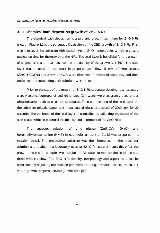
3.1.1 Chemical bath deposition growth of ZnO NRs
The chemical bath deposition is a two step growth technique for ZnO NRs
growth. Figure 3.1 is the schematic illustration of the CBD growth of ZnO NRs. First
step is to cover the substrate with a seed layer of ZnO nanoparticles which serve as a
nucleation sites for the growth of the NRs. The seed layer is beneficial for the growth
of aligned NRs and it can also control the density of the grown NRs [67]. The seed
layer that is used in our work is prepared as follow: 5 mM of zinc acetate
(Zn(CH3COO)2) and 2 mM of KOH were dissolved in methanol separately and then
under continuous stirring both solutions were mixed.
Prior to the start of the growth of ZnO NRs substrate cleaning is a necessary
step. Acetone, isopropanol and de-ionized (DI) water were separately used under
ultrasonication bath to clean the substrates. Then spin coating of the seed layer on
the substrate (plastic, paper and metal coated glass) at a speed of 3000 rpm for 30
seconds. The thickness of the seed layer is controlled by adjusting the speed of the
spin coater which can control the density and alignment of the ZnO NRs.
The aqueous solution of zinc nitrate (Zn(NO3)2. 6H2O) and
hexamethylenetetramine (HMT) in equimolar amount of 0.1 M was prepared in a
reaction vessel. The pre-seeded substrate was then immersed in the precursor
solution and loaded in a laboratory oven at 50 oC for several hours (h). After the
growth process the samples were soaked in DI water to remove the residuals and
dried with N2 blow. The ZnO NRs density, morphology and aspect ratio can be
controlled by adjusting the reaction parameters like e.g. precursor concentration, pH
value, growth temperature and growth time [68].
Synthesis and characterization of nanomaterials
15
Figure 3.1. Schematic diagram of the CBD growth of ZnO NRs.
3.1.2 Characterization of ZnO NRs
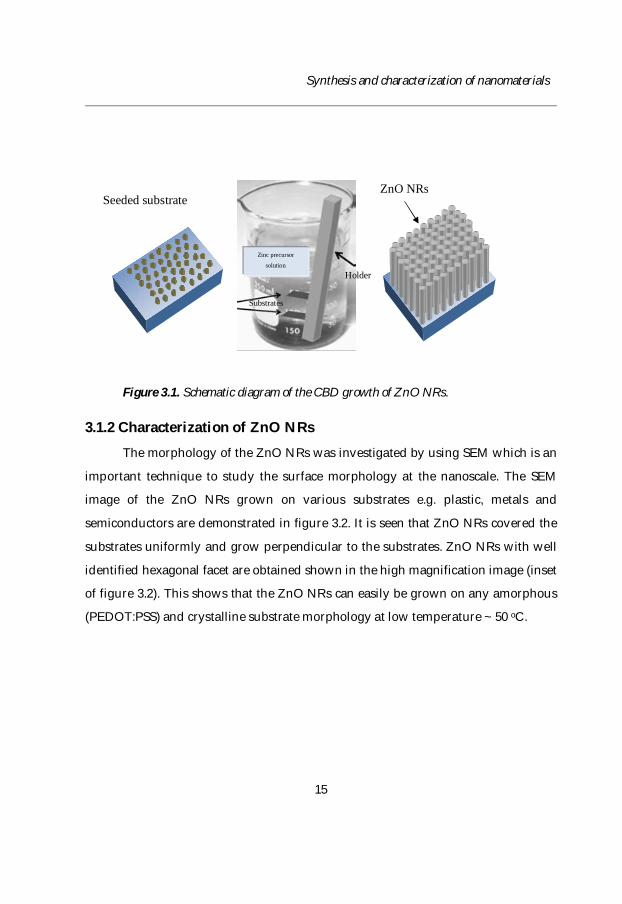
The morphology of the ZnO NRs was investigated by using SEM which is an
important technique to study the surface morphology at the nanoscale. The SEM
image of the ZnO NRs grown on various substrates e.g. plastic, metals and
semiconductors are demonstrated in figure 3.2. It is seen that ZnO NRs covered the
substrates uniformly and grow perpendicular to the substrates. ZnO NRs with well
identified hexagonal facet are obtained shown in the high magnification image (inset
of figure 3.2). This shows that the ZnO NRs can easily be grown on any amorphous
(PEDOT:PSS) and crystalline substrate morphology at low temperature ~ 50 oC.
Zinc precursor
solution
Holder
Substrates
Seeded substrate ZnO NRs
Synthesis and characterization of nanomaterials
16
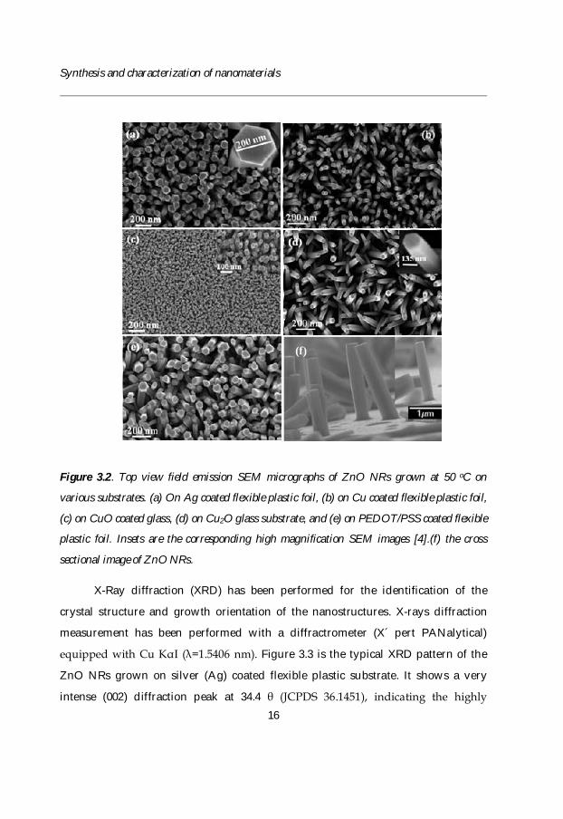
Figure 3.2. Top view field emission SEM micrographs of ZnO NRs grown at 50 oC on
various substrates. (a) On Ag coated flexible plastic foil, (b) on Cu coated flexible plastic foil,
(c) on CuO coated glass, (d) on Cu2O glass substrate, and (e) on PEDOT/PSS coated flexible
plastic foil. Insets are the corresponding high magnification SEM images [4].(f) the cross
sectional image of ZnO NRs.
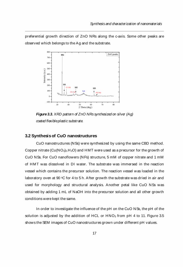
X-Ray diffraction (XRD) has been performed for the identification of the
crystal structure and growth orientation of the nanostructures. X-rays diffraction
measurement has been performed with a diffractrometer (X´ pert PANalytical)
equipped with Cu KαI (λ=1.5406 nm). Figure 3.3 is the typical XRD pattern of the
ZnO NRs grown on silver (Ag) coated flexible plastic substrate. It shows a very
intense (002) diffraction peak at 34.4 θ (JCPDS 36.1451), indicating the highly
(f)
Synthesis and characterization of nanomaterials
17
preferential growth direction of ZnO NRs along the c-axis. Some other peaks are
observed which belongs to the Ag and the substrate.
Figure 3.3. XRD pattern of ZnO NRs synthesized on silver (Ag)
coated flexible plastic substrate.
3.2 Synthesis of CuO nanostructures
CuO nanostructures (NSs) were synthesized by using the same CBD method.
Copper nitrate (Cu(NO3)2.H2O) and HMT were used as a precursor for the growth of
CuO NSs. For CuO nanoflowers (NFs) structure, 5 mM of copper nitrate and 1 mM
of HMT was dissolved in DI water. The substrate was immersed in the reaction
vessel which contains the precursor solution. The reaction vessel was loaded in the
laboratory oven at 90 oC for 4 to 5 h. After growth the substrate was dried in air and
used for morphology and structural analysis. Another petal like CuO NSs was
obtained by adding 1 mL of NaOH into the precursor solution and all other growth
conditions were kept the same.
In order to investigate the influence of the pH on the CuO NSs, the pH of the
solution is adjusted by the addition of HCL or HNO3 from pH 4 to 11. Figure 3.5
shows the SEM images of CuO nanostructures grown under different pH values.
30 40 50 60 70 80-100
0
100
200
300
400
500
600
700
800
220 (Ag)
103Sub
102
200 (Ag)
111 (Ag)
101
002
Inte
nsity
(a.u
.)
2 Theta (deg.)
ZnO peaks
Synthesis and characterization of nanomaterials
18
3.2.1. Characterization of CuO nanostructures
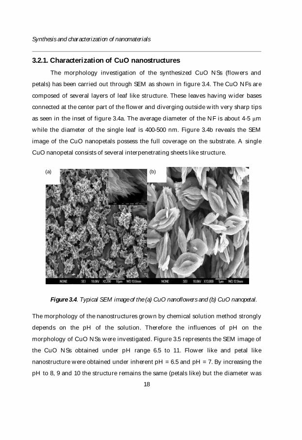
The morphology investigation of the synthesized CuO NSs (flowers and
petals) has been carried out through SEM as shown in figure 3.4. The CuO NFs are
composed of several layers of leaf like structure. These leaves having wider bases
connected at the center part of the flower and diverging outside with very sharp tips
as seen in the inset of figure 3.4a. The average diameter of the NF is about 4-5 µm
while the diameter of the single leaf is 400-500 nm. Figure 3.4b reveals the SEM
image of the CuO nanopetals possess the full coverage on the substrate. A single
CuO nanopetal consists of several interpenetrating sheets like structure.
Figure 3.4. Typical SEM image of the (a) CuO nanoflowers and (b) CuO nanopetal.
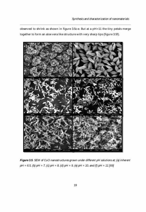
The morphology of the nanostructures grown by chemical solution method strongly
depends on the pH of the solution. Therefore the influences of pH on the
morphology of CuO NSs were investigated. Figure 3.5 represents the SEM image of
the CuO NSs obtained under pH range 6.5 to 11. Flower like and petal like
nanostructure were obtained under inherent pH = 6.5 and pH = 7. By increasing the
pH to 8, 9 and 10 the structure remains the same (petals like) but the diameter was
(b) (a)
Synthesis and characterization of nanomaterials
19
observed to shrink as shown in figure 3.5c-e. But at a pH=11 the tiny petals merge
together to form an aloe vera like structure with very sharp tips (figure 3.5f).
Figure 3.5. SEM of CuO nanostructures grown under different pH solutions at; (a) inherent
pH = 6.5, (b) pH = 7, (c) pH = 8, (d) pH = 9, (e) pH = 10, and (f) pH = 11 [69]
Synthesis and characterization of nanomaterials
20
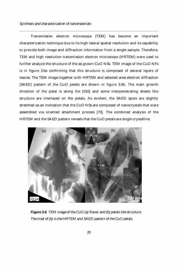
Transmission electron microscope (TEM) has become an important
characterization technique due to its high lateral spatial resolution and its capability
to provide both image and diffraction information from a single sample. Therefore,
TEM and high resolution transmission electron microscope (HRTEM) were used to
further analyze the structure of the as grown CuO NSs. TEM image of the CuO NFs
is in figure 3.6a confirming that this structure is composed of several layers of
leaves. The TEM image together with HRTEM and selected area electron diffraction
(SAED) pattern of the CuO petals are shown in figure 3.6b. The main growth
direction of the petal is along the [010] and some interpenetrating sheets like
structure are interlaced on the petals. As evident, the SAED spots are slightly
stretched as an indication that the CuO NSs are composed of nanocrystals that were
assembled via oriented attachment process [70]. The combined analysis of the
HRTEM and the SAED pattern reveals that the CuO petals are single crystalline.
Figure 3.6. TEM image of the CuO (a) flower and (b) petals like structure.
The inset of (b) is the HRTEM and SAED pattern of the CuO petals.
(b) (a)
Synthesis and characterization of nanomaterials
21
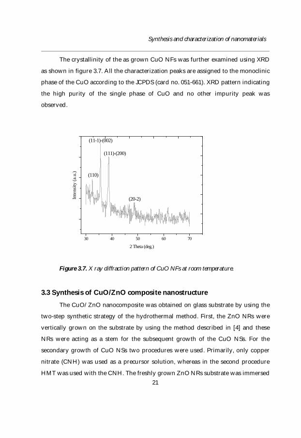
The crystallinity of the as grown CuO NFs was further examined using XRD
as shown in figure 3.7. All the characterization peaks are assigned to the monoclinic
phase of the CuO according to the JCPDS (card no. 051-661). XRD pattern indicating
the high purity of the single phase of CuO and no other impurity peak was
observed.
Figure 3.7. X ray diffraction pattern of CuO NFs at room temperature.
3.3 Synthesis of CuO/ZnO composite nanostructure
The CuO/ZnO nanocomposite was obtained on glass substrate by using the
two-step synthetic strategy of the hydrothermal method. First, the ZnO NRs were
vertically grown on the substrate by using the method described in [4] and these
NRs were acting as a stem for the subsequent growth of the CuO NSs. For the
secondary growth of CuO NSs two procedures were used. Primarily, only copper
nitrate (CNH) was used as a precursor solution, whereas in the second procedure
HMT was used with the CNH. The freshly grown ZnO NRs substrate was immersed
30 40 50 60 70
Inte
nsity
(a.u
.)
2 Theta (deg.)
(110)
(11-1)-(002)
(111)-(200)
(20-2)
Synthesis and characterization of nanomaterials
22
having face upward in the precursor solutions and heated for 4-5 h at 60 oC. Dense
hierarchical CuO NSs were selectively assembled on the ZnO NRs and producing a
corals-like CuO/ZnO nanocomposite.
3.3.1 Characterization of CuO/ZnO composite nanostructure
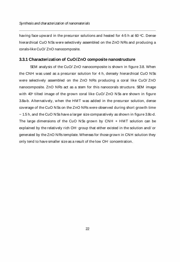
SEM analysis of the CuO/ZnO nanocomposite is shown in figure 3.8. When
the CNH was used as a precursor solution for 4 h, densely hierarchical CuO NSs
were selectively assembled on the ZnO NRs producing a coral like CuO/ZnO
nanocomposite. ZnO NRs act as a stem for this nanocorals structure. SEM image
with 40o tilted image of the grown coral like CuO/ZnO NSs are shown in figure
3.8a-b. Alternatively, when the HMT was added in the precursor solution, dense
coverage of the CuO NSs on the ZnO NRs were observed during short growth time
~ 1.5 h, and the CuO NSs have a larger size comparatively as shown in figure 3.8c-d.
The large dimensions of the CuO NSs grown by CNH + HMT solution can be
explained by the relatively rich OH- group that either existed in the solution and/or
generated by the ZnO NRs template. Whereas for those grown in CNH solution they
only tend to have smaller size as a result of the low OH- concentration.
Synthesis and characterization of nanomaterials
23
Figure 3.8: a) SEM image of CuO/ZnO nanocorals grown using CNH precursor solution
for 4 h, b) 40o tilted view SEM images of CuO/ZnO nanocorals, c) CuO/ZnO
nanostructures grown for short time of 0.5 or 1.5 h using either CNH+HMT or CNH,
respectively, and d) CuO/ZnO NSs grown using CNH+HMT for 1.5 h at 60 oC.
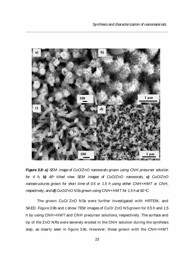
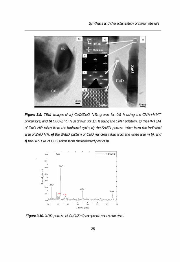
The grown CuO/ZnO NSs were further investigated with HRTEM, and
SAED. Figure 3.9b and c show TEM images of CuO/ZnO NS grown for 0.5 h and 1.5
h by using CNH+HMT and CNH precursor solutions, respectively. The surface and
tip of the ZnO NRs were severely eroded in the CNH solution during the synthesis
step, as clearly seen in figure 3.9c. However, those grown with the CNH+HMT
1 µm
1 µm 100
100
a) b)
c) d)
Synthesis and characterization of nanomaterials
24
solution demonstrated less etching effect on the ZnO NR as shown in the TEM of
figure 3.9b. This result is in good agreement with the influence of the weak acidic
conditions on the ZnO NRs. Moreover, CuO NSs grown using different precursor
solutions may greatly affect their shape and dimensions which is concluded by
comparing the TEM image of figure 3.9b-c. The SEAD and the HRTEM of CuO NS
grown on ZnO NR are presented in figure 3.9f-g, respectively. These results reveals
that CuO NS is preferentially grown along the (020) plane of the monoclinic
structure of CuO and highly crystalline in nature with straight and parallel lattice
fringes (d). Figures 3.9d-e represents the HRTEM and the SAED of ZnO NR taken
from the part indicated by the cycle. It is evident from figure 3.9d that ZnO NR was
grown along the [0001], and that the lattice spacing between two neighboring fringes
is 0.52 nm. The SEAD pattern shown in figure 3.9e is indexed to the [0001] direction
of the wurtzite-phase ZnO and it demonstrates the single-crystal nature of the ZnO
NR. No obvious epitaxial relationship was found (not shown here) between the CuO
NSs and the ZnO NRs which agrees well with what is previously reported for
ZnO/CuO hierarchical nanotrees array [66].
The crystal structure obtained was investigated by XRD. Figure 3.10 shows
the XRD pattern of CuO/ZnO composite nanostructure. Both ZnO and CuO peaks
appears in the pattern which confirms the presence of both materials. Two peaks at
2θ value of 35.5o and 38.7o belong to the monoclinic CuO while all other peaks are
related to the ZnO wurtzite structure [71].
Synthesis and characterization of nanomaterials
25
Figure 3.9: TEM images of a) CuO/ZnO NSs grown for 0.5 h using the CNH+HMT
precursors, and b) CuO/ZnO NSs grown for 1.5 h using the CNH solution, c) the HRTEM
of ZnO NR taken from the indicated cycle, d) the SAED pattern taken from the indicated
area of ZnO NR, e) the SAED pattern of CuO nanoleaf taken from the white area in b), and
f) the HRTEM of CuO taken from the indicated part of b).
.
Figure 3.10. XRD pattern of CuO/ZnO composite nanostructures.
30 35 40 45 50 55 60 65
0
10
20
30
40
50
60
70
CuOZnO
ZnO
ZnO
ZnO
Inte
nsity
(a.u
.)
2 Theta (deg)
CuO/ZnOZnO
CuO

Fabrication and characterization of devices
27
Chapter 4
Fabrication and characterization of devices
The synthesized ZnO and CuO nanostructures have a great potential to be used in a wide
range of applications. This chapter deals with some applications of these nanostructures. In
particular, ZnO NRs emerge versatile characteristics useful in extensive fields. Therefore,
efforts have been devoted to the fabrication of ZnO NRs hybrid LEDs to achieve full color
emission. Semiconductor parameter analyzer was used for electrical characterization (I-V) of
the fabricated LEDs. The absorption and the photoluminescence (PL) spectra were measured
with UV-VIS-NIR spectrometer and laser source with specific excitation source. PL is
usually employed to investigate the optical properties of nanostructures [72].
Electroluminescence (EL) is very useful opto-electrical technique which helps to understand
the emission characteristics of the devices [73]. In this thesis the EL spectra were examined
using an Andor-Newton CCD. Moreover, CuO nanoflowers were used to fabricate an
electrochemical pH sensor, and the potentiometric response of pH sensor was measure using
Metrohm pH meter. CuO NSs were also used as catalyst to degrade the organic dyes without
using any irradiation source.
4.1 ZnO NRs/polymers hybrid LEDs
The advent of lighting to human started with fire, and from that time the
obsession with lighting took hold and whisked itself through the ages leading to the
light emitting diodes (LEDs). The lighting area is facing a unique technology
breakthrough with the emergence of LEDs. LED based lighting is though a recent
phenomenon, but LED deployment in this field of application now seems inevitable.
Nevertheless, the invention of blue LEDs in early 1980's gave access to white light
combining red, blue and green LEDs [74]. LEDs have advantages over conventional
light sources, such as higher efficiency, longer life, smaller size, and enhanced
controllability, among other characteristics. LEDs have been seen in successful
Fabrication and characterization of devices
28
applications, such as displays, traffic signals, automotive parts, backlighting, accent
lighting, as well as in other applications. The multiple benefits of LEDs and the
continuous increase in their performance allied to the decrease of their
manufacturing costs are likely to make them competitive when compared to
fluorescent lamps and tubes. So far, different types of materials are used to fabricate
white light emitting diodes but still much effort is required to improve the
performance.
With the feature of wide bandgap and large excitonic energy, ZnO was
considered as a prospective material for fabricating light emitting diodes. The
development of p-type doping of ZnO is rapidly growing and many research articles
have been reported [75-78]. But, reproducible p-ZnO with high mobility and high
hole concentration is still difficult. Therefore, the fabrication of homojunction ZnO
LEDs is yet not resolved. To circumvent this problem, an alternate approach was to
develop hybrid p-n junction LEDs, which are composed of heterojunction between
n-ZnO and other p-type materials. Variety of p-type materials such as Si [79], GaN
[80, 81], SiC [82, 83] were used to realize hybrid junctions with ZnO. However, these
materials are expensive and limit the choice to produce cheap flexible devices. To
get an advantage of low temperature ZnO growth on flexible plastic and paper
substrates, p-type polymers are a good choice. Polymers are very promising
materials having many advantages like solution processable, flexible, light weighted
and robust. The easy processing of polymers offers the potential for enormous cost-
savings in many applications. They enable the homogeneous illumination of large
area and lightweight displays can be produced on a variety of flexible substrates.
This provides the ability to conform, bend or roll a display into any shape. One of
the key advantages of the conjugated polymer is the tunability of the emissive
colors. Blue light can be down converted into green and red emission by simply
doping or blending the blue emitter with lower bandgap polymers [84]. Thus,
hybrids ZnO/polymer LEDs combine the advantage of both organic and inorganic

Fabrication and characterization of devices
29
semiconductors. These hybrids LEDs are superior to all-organic counterparts
because the optically active component is inorganic nanostructures, which usually
has a higher carrier mobility and lifetime than organic materials [85, 86]. The
emissions of hybrid LEDs exhibit white light impression which covers the whole
visible region. Moreover, vertical ZnO NRs are beneficial in hybrid LEDs because
NRs are like natural waveguiding cavities for causing the emitted light to travel to
the top of the device enhancing the light extraction efficiency from the LED surface
[87]. Although no output power data are yet available for ZnO NR/polymer LEDs,
the published internal quantum efficiency (IQE) results obtained from ZnO NRs are
promising. ZnO NRs grown by the low temperature process showed IQE of 28%
while a higher value of 52% for the IQE of the NBE emission was report for ZnO
NRs grown by the metal organic chemical vapour deposition (MOCVD) [88-90].
ZnO NRs are used to fabricate hybrid ZnO NRs/polymer LEDs. Two
nonconventional substrates, disposable paper and flexible plastic are used as a
substrate for the device fabrication. Paper is ubiquitous in everyday life and a truly
low-cost substrate. It has also recently been considered as a potential substrate for
low-cost flexible electronics [91]. In addition to this, paper is also environmentally
friendly, since it is recyclable and made of renewable raw materials. Usually paper is
insulting and it can degrade in water, therefore the pretreatment of the paper
substrate is essential. For this purpose a cyclotene layer (BCB 4022-35 Dow
Chemical’s) was spin coated on the paper substrate, followed by vacuum baking at
110 oC for 1 h. The cyclotene barrier layer reduces the surface roughness and
protects the surface of the paper from the water nutrient solution. Then PEDOT:PSS
(3,4-ethylenedioxythiophene) poly(styrenesulfonate) solution was spin coated on the
substrate at a speed of 2000 rpm followed by baking at 70 oC for 2 h. Next spin
coating of a blue light emitting polymer (PFO) at a speed of 2000 rpm and anneal at
70 oC for 10 minutes was performed. Finally ZnO NRs were grown on the PFO by
using the method mentioned above [4].
Fabrication and characterization of devices
30
To fabricate hybrid LEDs on plastic substrate, commercially available
PEDOT:PSS coated plastic was used due to its flexibility, transparency in the visible
region and good electrical properties. Prior to spin coating the polymer, the
substrate was cleaned by using acetone, isopropanol and DI water subsequently.
Two polymers the PFO (blue emitting) and the MEH PPV (red emitting) were used
separately and their blend prepared with the ratio of 9:1 was also used. Some area of
the substrate was covered to serve as a bottom contact. Then spin coat the polymer
at a speed of 2000 rpm and soft bake for 10-15 min. ZnO NRs were grown on the
polymer layer by following the same procedure discussed in previous chapter.
Figure 4.1. Schematic illustration of the device fabrication.
To complete the device, spin coat the polymethyl methacrylate (PMMA) layer
which serve as an insulator to fill the gap between the ZnO NRs. Reactive ion
etching (RIE) was used to etch the PMMA layer to expose the tips of the ZnO NRs.
(f)
(d
(a) (b
(c)
(e)
Fabrication and characterization of devices
31
Finally evaporate the aluminum (Al) top contact on ZnO NRs while the bottom
contact on the PEDOT:PSS was achieved by applying silver (Ag) paste. A schematic
diagram of the fabricated LED is shown in figure 4.1.
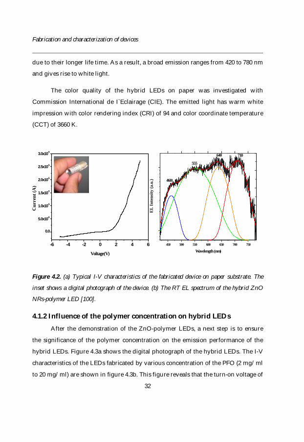
4.1.1 Characterization of hybrid LEDs on disposable paper substrates
Current-voltage (I-V) characteristics of LEDs give the key information to
judge the performance/quality of the fabricated diodes [92-94]. Figure 4.2a shows I-
V characteristics of the fabricated ZnO-polymer LEDs consisting of
Ag/PEDOT:PSS/PFO/ZnO NRs/Al. The I-V characteristics indicate the rectifying
behavior of the diode. The inset of figure 4.2a shows a photograph of the folded
substrates and no observable changes were noticed by rolling or bending the
substrates, which demonstrates the good adhesion of the PFO/ZnO NRs structure.
The room temperature EL of the hybrid LEDs is shown in figure 4.2b. This EL
reveals a broad spectrum covering the visible spectrum from 420 nm to 720 nm. The
blue peak appeared at 460 nm belongs to the PFO and is attributed to exciton
emission and its vibronic progression from non-interacting single chains [95]. The
broad green emission appearing at 555 nm is the famous green band emission due to
deep level defects in ZnO. This peak has been reported to be in this region,
especially in low temperature grown ZnO nanorods [96]. The PFO has also a defect
emission in this range i.e. around 520 nm due to the keto/fluorenone defects that
might be intrinsic during synthesis or generated during the device fabrication and
operation [97, 98]. The peaks at 640 nm and 710 nm belong to oxygen interfacial
defects [99]. The light emission in the ZnO NRs hybrid LED suggests that it can be
attributed to both the blue emission from PFO and the ZnO defects related
emissions. The interaction between the ZnO NRs surface and the PFO molecule
makes the PFO link up with ZnO and leads to ZnO NRs/PFO interface. The electron
existing at the interface between the conduction band edge of the ZnO NRs and the
lowest unoccupied molecular orbital of the PFO layer slowly drops to the lower state
Fabrication and characterization of devices
32
due to their longer life time. As a result, a broad emission ranges from 420 to 780 nm
and gives rise to white light.
The color quality of the hybrid LEDs on paper was investigated with
Commission International de I`Eclairage (CIE). The emitted light has warm white
impression with color rendering index (CRI) of 94 and color coordinate temperature
(CCT) of 3660 K.
Figure 4.2. (a) Typical I-V characteristics of the fabricated device on paper substrate. The
inset shows a digital photograph of the device. (b) The RT EL spectrum of the hybrid ZnO
NRs-polymer LED [100].
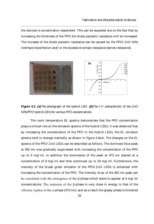
4.1.2 Influence of the polymer concentration on hybrid LEDs
After the demonstration of the ZnO-polymer LEDs, a next step is to ensure
the significance of the polymer concentration on the emission performance of the
hybrid LEDs. Figure 4.3a shows the digital photograph of the hybrid LEDs. The I-V
characteristics of the LEDs fabricated by various concentration of the PFO (2 mg/ml
to 20 mg/ml) are shown in figure 4.3b. This figure reveals that the turn-on voltage of
-6 -4 -2 0 2 4 6
0.0
5.0x10⁻⁶
1.0x10⁻⁵
1.5x10⁻⁵
2.0x10⁻⁵
2.5x10⁻⁵
3.0x10⁻⁵
Cur
rent
(A)
Voltage(V)
450 500 550 600 650 700 750
E
L In
tens
ity (a
.u.)
Wavelength (nm)
460
555
710640
Fabrication and characterization of devices
33
the devices is concentration dependent. This can be expected due to the fact that by
increasing the thickness of the PFO the diode parasitic resistance will be increased.
The increase of the diode parasitic resistance can be caused by the PFO/ZnO NRs
interface imperfection and/or the excessive contact resistance (series resistance).
Figure 4.3. (a)The photograph of the hybrid LED. (b)The I-V characteristic of the ZnO
NRs/PFO hybrid LEDs for various PFO concentrations.
The room temperature EL spectra demonstrate that the PFO concentration
plays a critical role on the emission spectra of the hybrid LEDs. It was observed that
by increasing the concentration of the PFO in the hybrid LEDs, the EL emission
spectra tend to change markedly as shown in figure 4.4a-b. The changes on the EL
spectra of the PFO/ZnO LEDs can be described as follows. The dominant blue peak
at 452 nm was gradually suppressed with increasing the concentration of the PFO
up to 6 mg/ml. In addition the dominance of the peak at 473 nm started at a
concentration of 8 mg/ml and then continued up to 20 mg/ml. Furthermore, the
intensity of the broad green emission of the PFO/ZnO LEDs is enhanced with
increasing the concentration of the PFO. The intensity drop of the 452 nm peak can
be correlated with the emergence of the β-phase which starts to appear at 6 mg/ml
concentrations. The emission of the β-phase is very close in energy to that of the
vibronic replica of the α-phase (473 nm), and as a result the glassy phase is hindered
-6 -4 -2 0 2 4 6 8 10
-0.08
-0.06
-0.04
-0.02
0.00
0.02
0.04
0.06
0.08
0.10
Cur
rent
(mA
)
Voltage (V)
2mg 4mg 6mg 8mg 10mg 20mg
(b)(a)
Fabrication and characterization of devices
34
by the formation of the β-phase [101]. The drop in the first peak (452 nm) of the EL
spectra implies either a fast and effective energy transfer from the α-phase to the β-
phase domain [102] or the β-phase may act as low-energy traps for the excitons
because it has a smaller energy gap compared to the α-phase [103]. Another change
which was observed in the EL spectrum is the enhancement of the green peak. This
can be originating from the increased quantity of fluorenone defects that were
introduced at larger concentrations (thickness) or the increased density of ZnO NRs
at higher PFO concentrations, and/or due to both effects. Simultaneously, two
processes involved in the green band emission of the PFO: first energy transfer from
the excitons on the PFO main chain to the fluorenone defect sites. Secondly, trapping
of excitons at the fluorenone defect sites followed by a subsequent radiative
recombination [55]. The fluorenone defects acts as a low-energy trap, and so it is
expected that there will be a competition between the β-phase and the fluorenone
defects for the excitons that were created within the PFO thin film [101].
To confirm our finding that the effect of the injected carriers of the defects
emission from the PFO by the electrochemical oxidation of the polymer chains, we
performed current dependent EL measurements. The results are shown in figure
4.5c. Interestingly at low injection currents (0.3- 0.6 mA) the EL spectrum shows
identical blue peaks as discussed before i.e. (452 nm and 470 nm). At a high injection
current a new blue peak was observed in the EL spectrum which was correlated to
the creation of a new chemical species on the PFO chain. Furthermore, the green
emission peak was also enhanced with increasing the injection current. The current
flowing through the polymer is also believed to play a crucial role in the oxidation of
the polymer. During the electro-oxidation process of the PFO fluorenone defects are
formed which in turns increase the green emission over the blue one.
The corresponding Commission Internationale de I´Eclairage (CIE)
chromaticity coordinates of the spectra at different concentrations are shown in
Fabrication and characterization of devices
35
figure 4.4d. The emission color of the LEDs changed from bluish white with color
coordinates (0.259, 0.312) to greenish white (0.309, 0.418) with increasing
concentration of the PFO. While the Correlated Color Temperature is decreases from
11741 K to 6196 K.
Figure 4.4. (a) and (b) electroluminescence spectra of the hybrid LEDs having PFO
concentration from 2mg/ml to 20mg/ml. (c) EL spectra of the ZnO NRs/PFO (2mg/ml) LED
at low and high injections current. (d) Chromaticity diagram (CIE coordinates) for all
fabricated LEDs illustrating the emission color change from bluish to greenish white.
4.1.3 Effect of the polymer emission on the EL of hybrid LEDs
The choice of the polymers with proper concentration is also critical to the
emitted color in ZnO NRs/polymer hybrid LEDs. The emission spectra can be tuned
400 450 500 550 600 650 700 7500
20000
40000
60000
80000 2mg 4mg 6mg 8mg
Inte
nsity
(a.u
)
Wavelength (nm)
(a)
400 450 500 550 600 650 700 7500
20000
40000
60000
80000
Inte
nsity
(a.u
)
Wavelength (nm)
2mg 10mg 20mg
(b)
400 450 500 550 600 650 700 750 800-1x10³
0
1x10³
2x10³
3x10³
4x10³
5x10³
6x10³
0.3 mA 5.0 mA
Wavelength (nm)
Inte
nsity
(a.u
)
PFO (2 mg/ml)451
470
465
505540
536(c)
0.0
2.0x10³
4.0x10³
6.0x10³
8.0x10³
Inte
nsity
(a.u
)
(d)
Fabrication and characterization of devices
36
by selecting proper ratio of the different polymers. Therefore, we demonstrate EL
and colour characteristics of organic-inorganic LEDs made from different p-type
polymer configurations with n-type inorganic ZnO NRs grown at low temperature
on flexible PEDOT:PSS coated plastic substrate.
Three types of LEDs have been fabricated, these were
PEDOT:PSS/PFO/ZnO/Al denoted as LED A; PEDOT:PSS/MEH-PPV/ZnO/Al
denoted as (LED B) and PEDOT:PSS/PFO:MEH-PPV/ZnO/Al denoted as (LED C).
The PFO and MEH-PPV blend was prepared with a molar ratio of 9:1 respectively.
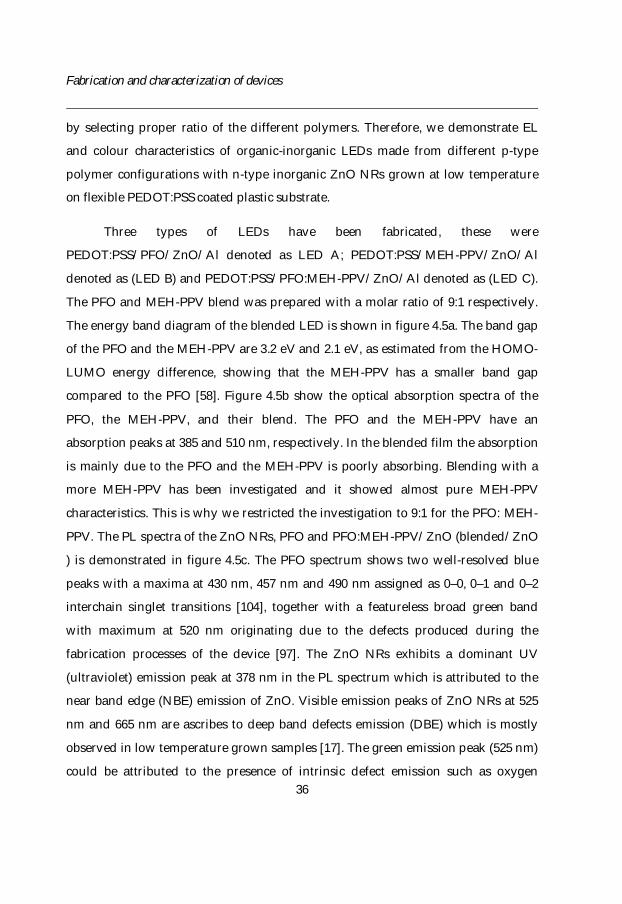
The energy band diagram of the blended LED is shown in figure 4.5a. The band gap
of the PFO and the MEH-PPV are 3.2 eV and 2.1 eV, as estimated from the HOMO-
LUMO energy difference, showing that the MEH-PPV has a smaller band gap
compared to the PFO [58]. Figure 4.5b show the optical absorption spectra of the
PFO, the MEH-PPV, and their blend. The PFO and the MEH-PPV have an
absorption peaks at 385 and 510 nm, respectively. In the blended film the absorption
is mainly due to the PFO and the MEH-PPV is poorly absorbing. Blending with a
more MEH-PPV has been investigated and it showed almost pure MEH-PPV
characteristics. This is why we restricted the investigation to 9:1 for the PFO: MEH-
PPV. The PL spectra of the ZnO NRs, PFO and PFO:MEH-PPV/ZnO (blended/ZnO
) is demonstrated in figure 4.5c. The PFO spectrum shows two well-resolved blue
peaks with a maxima at 430 nm, 457 nm and 490 nm assigned as 0–0, 0–1 and 0–2
interchain singlet transitions [104], together with a featureless broad green band
with maximum at 520 nm originating due to the defects produced during the
fabrication processes of the device [97]. The ZnO NRs exhibits a dominant UV
(ultraviolet) emission peak at 378 nm in the PL spectrum which is attributed to the
near band edge (NBE) emission of ZnO. Visible emission peaks of ZnO NRs at 525
nm and 665 nm are ascribes to deep band defects emission (DBE) which is mostly
observed in low temperature grown samples [17]. The green emission peak (525 nm)
could be attributed to the presence of intrinsic defect emission such as oxygen
Fabrication and characterization of devices
37
vacancies or zinc vacancies while the orange-red emission is due to the transition
from Zni to Oi [105, 106].
Figure 4.5. (a) The energy band diagram of LED C formed using the blended polymers. (b)
Absorption spectra of the PFO, the MEH-PPV and 9:1 blend of the PFO: MEH-PPV V
polymers. (c) Photoluminescence spectra of ZnO NRs, PFO and blended polymer/ZnO. (d)
Electroluminescence spectra of the three LEDs[107].
The blended/ZnO NRs PL shows that the PFO blue peaks and ZnO NBE are at the
same positions as we discussed above, while the ZnO NRs DBE peaks strongly
overlapped with MEH-PPV (orange-red) peaks. Because on one hand the ZnO NRs
are densely standing on top of the polymer layer with their length around ∼2 µm.
300 400 500 600 700
0.00
0.04
0.08
0.12
0.16
0.20
Abs
orpt
ion
(a.u
.)
Wavelength (nm)
MEH PPV PFO Blended PFO:MEHPPV
(b)
400 450 500 550 600 650 700 750 8000
500
1000
1500
2000
2500
3000
3500
4000
4500
Inte
nsity
(a.u
)
Wavelength (nm)
LED ALED C LED B
(d)
(a)
400 500 600 700 800-5000
0
5000
10000
15000
20000
25000
30000
35000
40000
45000
Inte
nsity
(a.u
.)
Wavelength (nm)
PFO ZnO Blended/ZnO
430457
378
(c)
Fabrication and characterization of devices
38
On the other hand, the PL measurements are very sensitive to the sample surface
and highly suppressing in the bulk contribution; therefore, most of the PL detected
intensity will originate from the top part of the sample (ZnO NRs). The featured
peaks at ∼585 nm and 615 nm can be ascribed to the overlapped emission of the
MEH PPV with the defect emission of ZnO. The emission peak at 585 nm of the
MEH PPV is assigned to single chain exciton transition, whereas the peak at ∼ 615
nm is due to the intrinsic vibronic structure [108].
The room temperature EL of the three LEDs under forward bias is depicted in
figure 4.5d. For LED A (PFO/ZnO), the emission peaks are discussed in the
previous part. LED B (MEH-PPV/ZnO) has an extended emission from 575 nm to
750 nm with a peak at 608 nm, which correspond to the MEH-PPV due to the PPV
backbone that arises from the relaxation of the excited Π-electrons to the ground
state and the shoulder at 640 nm is related to interchain states [109]. The peaks
appeared in the EL spectrum is originating from the MEH-PPV, because the
potential barrier for electrons is 1.2 eV and the mobility of electrons in the ZnO is
higher than that of holes in the MEH-PPV so the recombination primarily occurs in
the MEH-PPV side. For LED C the EL emission covering the entire visible emission,
the blue peak at ~ 455 nm belongs to the PFO, while the green emission is from the
ZnO DBE along with the orange-red emission from the MEH-PPV are completely
intermixed yielding a broad visible emission. It is seen that even at very low
concentration of the MEH-PPV in the blend, the energy transfer is predominant and
the device gives intense emission from the MEH-PPV. The PFO emission is
relatively low but is still high enough to influence the colour quality of the device.
The emission from both polymers is due to the incomplete energy transfer [110].
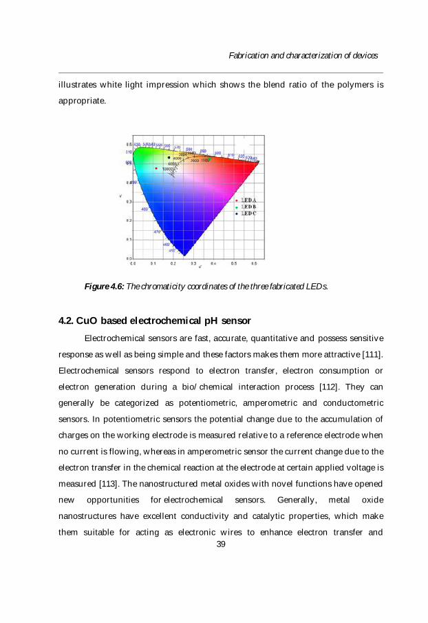
In figure 4.6 the CIE 1931 color space chromaticity diagram in the (x, y)
coordinate system of the fabricated LEDs are plotted. A bluish white impression can
be seen for LED A while orange-red impression is observed for LED B. The LED C
Fabrication and characterization of devices
39
illustrates white light impression which shows the blend ratio of the polymers is
appropriate.
Figure 4.6: The chromaticity coordinates of the three fabricated LEDs.
4.2. CuO based electrochemical pH sensor
Electrochemical sensors are fast, accurate, quantitative and possess sensitive
response as well as being simple and these factors makes them more attractive [111].
Electrochemical sensors respond to electron transfer, electron consumption or
electron generation during a bio/chemical interaction process [112]. They can
generally be categorized as potentiometric, amperometric and conductometric
sensors. In potentiometric sensors the potential change due to the accumulation of
charges on the working electrode is measured relative to a reference electrode when
no current is flowing, whereas in amperometric sensor the current change due to the
electron transfer in the chemical reaction at the electrode at certain applied voltage is
measured [113]. The nanostructured metal oxides with novel functions have opened
new opportunities for electrochemical sensors. Generally, metal oxide
nanostructures have excellent conductivity and catalytic properties, which make
them suitable for acting as electronic wires to enhance electron transfer and
Fabrication and characterization of devices
40
improved sensing characteristics [114]. Also, nanostructure with high surface area-
to-volume ratio leads to a short diffusion distance of the analyte toward the
electrode surface, thereby providing a faster response and enhanced analytical
performance.
The pH determination is a strong prerequisite for many biochemical and
biological processes. The pH of a solution, biological and biochemical is vitally
important in order to use the solution effectively. The pH value of blood is an
important index for the human body, even a small change in the pH of the body
fluids can begin a problem in human body. Thus, pH measurements are vitally
important in many applications including medicine. The electrochemical pH sensors
have found use in several other areas, such as industrial hygiene, pollution
measurement and control, hazard monitoring, process control and combustion
control. Moreover, metal oxides have been widely reported to have pH- sensitivity
and therefore develop pH sensors based on these materials [115-119]. Prior to all
these, the production of faster, robust and cost efficient electrochemical sensors have
huge significance for the daily life diagnostics of pH.
Specifically, CuO nanostructures having a large surface area-to-volume ratio,
high surface reaction activity and biocompatibility. CuO is one of the interesting and
appropriate metal oxides for biosensing applications [120-122]. CuO flowers were
grown on gold coated glass substrate by the method mentioned in the previous
chapter. Electrochemical studies are conducted using a two-electrode configurations
consisting of CuO nanoflowers (NFs) as the working electrode and Ag/AgCl/Cl as a
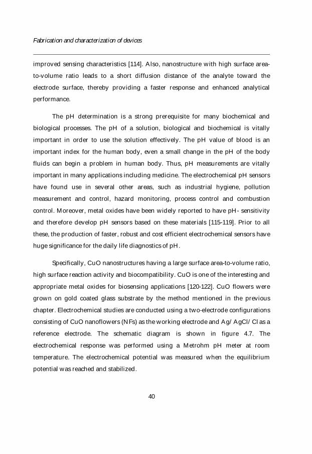
reference electrode. The schematic diagram is shown in figure 4.7. The
electrochemical response was performed using a Metrohm pH meter at room
temperature. The electrochemical potential was measured when the equilibrium
potential was reached and stabilized.
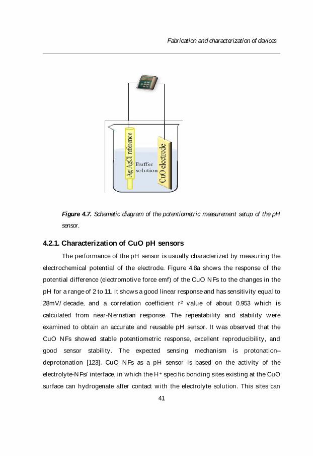
Fabrication and characterization of devices
41
Figure 4.7. Schematic diagram of the potentiometric measurement setup of the pH
sensor.
4.2.1. Characterization of CuO pH sensors
The performance of the pH sensor is usually characterized by measuring the
electrochemical potential of the electrode. Figure 4.8a shows the response of the
potential difference (electromotive force emf) of the CuO NFs to the changes in the
pH for a range of 2 to 11. It shows a good linear response and has sensitivity equal to
28mV/decade, and a correlation coefficient r2 value of about 0.953 which is
calculated from near-Nernstian response. The repeatability and stability were
examined to obtain an accurate and reusable pH sensor. It was observed that the
CuO NFs showed stable potentiometric response, excellent reproducibility, and
good sensor stability. The expected sensing mechanism is protonation–
deprotonation [123]. CuO NFs as a pH sensor is based on the activity of the
electrolyte-NFs/interface, in which the H+ specific bonding sites existing at the CuO
surface can hydrogenate after contact with the electrolyte solution. This sites can
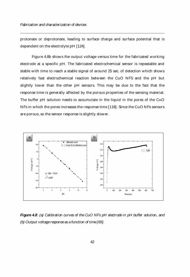
Fabrication and characterization of devices
42
protonate or deprotonate, leading to surface charge and surface potential that is
dependent on the electrolyte pH [124].
Figure 4.8b shows the output voltage versus time for the fabricated working
electrode at a specific pH. The fabricated electrochemical sensor is repeatable and
stable with time to reach a stable signal of around 25 sec. of detection which shows
relatively fast electrochemical reaction between the CuO NFS and the pH but
slightly lower than the other pH sensors. This may be due to the fact that the
response time is generally affected by the porous properties of the sensing material.
The buffer pH solution needs to accumulate in the liquid in the pores of the CuO
NFs in which the pores increases the response time [118]. Since the CuO NFs sensors
are porous, so the sensor response is slightly slower.
Figure 4.8: (a) Calibration curves of the CuO NFs pH electrode in pH buffer solution, and
(b) Output voltage response as a function of time [69].
2 4 6 8 10 12-200
-150
-100
-50
0
50
100
Vol
tage
(mV
)
pH
calibration curve Linear fit of calibration curve
y= -28x + 153.9
r 2= 0.997
0 100 200 300 400 500 600 700
1.40
1.42
1.44
1.46
1.48
1.50
1.52
1.54
Vol
tage
(V)
Time (sec)
4 ph
a b
Fabrication and characterization of devices
43
4.3. CuO nanostructures as a catalyst
With the increasing revolution in science and technology, there was a greater
demand on opting for new chemicals which could be used in various industrial
activities. Organic dyes are one from many new chemicals which could be used in
several industrial processes. Due to their large-scale production and extensive
applications, organic dyes have become an integral part of the industrial
wastewater. In fact, a huge amount of organic dyes are lost in the wastewater during
manufacturing and applications process [125, 126]. These dyes are harmful for
aquatic life and environmental. Various methods have been widely used to handle
the dye removal from wastewaters in order to comply with the environmental
regulations, which are becoming more crucial these days. In recent years,
heterogeneous photocatalysis processes are one of the most efficient methods for
destroying organic pollutants and dyes in aqueous media [127, 128]. Heterogeneous
photocatalysis is a process in which the degradation of organic pollutants is
governed by the combined actions of a semiconductor catalyst, an irradiation source
and an oxidizing agent. One parameter which plays crucial role in the enhancement
of the activity of the catalyst is the irradiation source. Mostly irradiation source
which are commonly used are expensive and pollutant. Therefore, degradation of
the organic dyes without any expensive irradiation source is of special interest,
making the development of suitable technologies for practical applications very
attractive. Hydrogen peroxide (H2O2) is a preferable oxidant because of the
simplicity of handling, the environmentally friendly nature of coproduct (water), the
high oxygen atom efficiency, and the versatility [129]. Moreover, utilization of the
H2O2 in catalytic reaction has great advantage to the environment and industry
because (i) it generates H2O as a sole by-product, (ii) it has a high content of active
oxygen species, and (iii) H2O2 is rather inexpensive [130]. The semiconductor
catalysts which are the core of the whole process are mostly metal oxides that can be
more appealing than the conventional chemical oxidation methods because metal
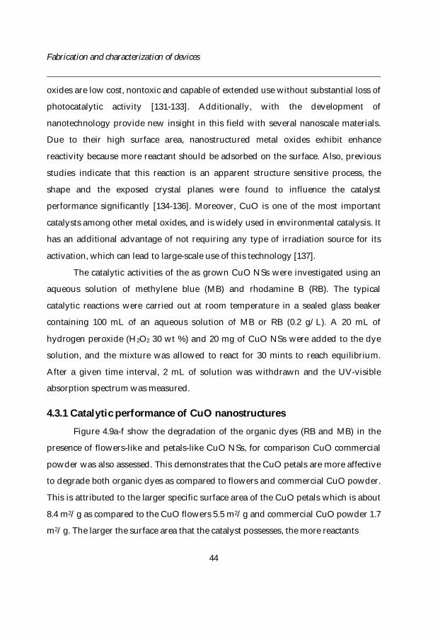
Fabrication and characterization of devices
44
oxides are low cost, nontoxic and capable of extended use without substantial loss of
photocatalytic activity [131-133]. Additionally, with the development of
nanotechnology provide new insight in this field with several nanoscale materials.
Due to their high surface area, nanostructured metal oxides exhibit enhance
reactivity because more reactant should be adsorbed on the surface. Also, previous
studies indicate that this reaction is an apparent structure sensitive process, the
shape and the exposed crystal planes were found to influence the catalyst
performance significantly [134-136]. Moreover, CuO is one of the most important
catalysts among other metal oxides, and is widely used in environmental catalysis. It
has an additional advantage of not requiring any type of irradiation source for its
activation, which can lead to large-scale use of this technology [137].
The catalytic activities of the as grown CuO NSs were investigated using an
aqueous solution of methylene blue (MB) and rhodamine B (RB). The typical
catalytic reactions were carried out at room temperature in a sealed glass beaker
containing 100 mL of an aqueous solution of MB or RB (0.2 g/L). A 20 mL of
hydrogen peroxide (H2O2 30 wt %) and 20 mg of CuO NSs were added to the dye
solution, and the mixture was allowed to react for 30 mints to reach equilibrium.
After a given time interval, 2 mL of solution was withdrawn and the UV-visible
absorption spectrum was measured.
4.3.1 Catalytic performance of CuO nanostructures
Figure 4.9a-f show the degradation of the organic dyes (RB and MB) in the
presence of flowers-like and petals-like CuO NSs, for comparison CuO commercial
powder was also assessed. This demonstrates that the CuO petals are more affective
to degrade both organic dyes as compared to flowers and commercial CuO powder.
This is attributed to the larger specific surface area of the CuO petals which is about
8.4 m2/g as compared to the CuO flowers 5.5 m2/g and commercial CuO powder 1.7
m2/g. The larger the surface area that the catalyst possesses, the more reactants
Fabrication and characterization of devices
45
Figure 4.9: (a-d) UV- visible absorption spectral changes of an aqueous solution of RB and
MB in presence of CuO flowers and petals, and H2O2.(e, f) Plots of the concentration ratio of
RB and MB in an aqueous solution against specific time intervals in presence or absence of
CuO .
300 400 500 600 700 800 900
0.0
0.2
0.4
0.6
0.8
1.0
1.2
Abs
orba
nce
(a.u
.)
Wavelength (nm)
0 hr 0.5 hr 1 hr 2 hr 3 hr 4 hr 5 hr 6 hr 7 hr 24 hr
CuO petals in MB (d)
0 5 10 15 20 25
0.0
0.1
0.2
0.3
0.4
0.5
0.6
0.7
0.8
0.9
1.0
1.1
C/C
0
Time (h)
CuO flower CuO powder CuO petals MB +H2O2
(f)
300 400 500 600 700 800 900-0.2
0.0
0.2
0.4
0.6
0.8
1.0
1.2
1.4
1.6
1.8
2.0
Abs
orba
nce
(a.u
.)
Wavelength (nm)
0hr 0.5 hr 1 hr 2hr 3hr 4hr 5hr 6hr 7hr 24hr
CuO flowers in MB (c)
0 1 2 3 4 50.0
0.2
0.4
0.6
0.8
1.0
C/C
o
Time (h)
CuO powder RB+H2O2 CuO flower CuO petals
(e)
300 400 500 600 700 800 900
0.0
0.2
0.4
0.6
0.8
1.0
1.2
Abs
orba
nce
(a.u
.)
Wavelength (nm)
0 hr 0.5 hr 1 hr 2 hr 3 hr 4 hr 5 hr
CuO flower in RB (a)
300 400 500 600 700 800 9000.0
0.2
0.4
0.6
0.8
1.0
1.2
1.4
1.6
Abs
orba
nce
(a.u
.)
Wavelength (nm)
0 hr 0.5 hr 1 hr 2 hr 3 hr 4 hr 5 hr
CuO petals in RB (b)
Fabrication and characterization of devices
46
(e.g., O2, OH-, and organic molecules) that should be adsorbed on its surface due to
an increase in the number of active sites, thus leading to higher catalytic activity
[138]. Moreover, the main process of the degradation of the dye is adsorption–
oxidation–desorption mechanism. The MB molecule and H2O2 were first adsorbed
on the surface of the nanostructures, and then free radical species of HO•, HOO•, or
O2•− were produced by the catalytic decomposition of H2O2. Theses free radicals
cause the destructive oxidation of the organic dye.
The fitting of the maximum absorbance plot vs. time suggest that these
catalytic degradations follow the pseudo-first-order reaction with respect to both
dyes [69] (shown in appended paper VI). This indicates that for both dyes the
degradation rates follow the order of CuO petals > CuO flowers > CuO commercial
powder. After demonstration of the catalytic activity of the CuO NSs their
reusability was checked, and it confirms that these NSs are useful for many cycles.
All these results conclude that as prepared CuO NSs could work as an effective and
reusable catalyst at room temperature without using any specific light source.
Conclusion and future work
47
Chapter 5
Conclusion and future work
The present work mainly covers ZnO and CuO nanostructures, study of their low
temperature growth, characterization and applications. This work is mainly divided
into: (i) Synthesis of ZnO NRs and fabricate hybrid LEDs (ii) CuO NSs growth and
applications and (iii) Synthesis and characterization of composite CuO/ZnO NSs.
Well aligned ZnO NRs were synthesized using the wet chemical method at 50 oC on various substrates in paper Ι. We found that lowering the growth temperature
is advantageous for the axial length of the ZnO NRs. The growth of ZnO NRs on
metal, semiconductor and polymer coated substrates is essential for various
applications. The low temperature method does not require any harsh fabrication
process on the target substrates which enables the use of nonconventional substrates
such as plastic, polymer and paper. Utilizing the compatibility of this method with
nonconventional substrates we synthesized ZnO NRs on flexible and disposable
substrates, which are likely to be integrated with future foldable and disposable
electronics. Low cost production is a main attraction of any product and ZnO
nanostructures has much potential to become the choice for cheap devices.
Therefore, we have studied ZnO NRs-based hybrid LEDs in this work. The ZnO
NRs were successfully utilized for white light emitting diodes (LEDs) on flexible
plastic and disposable paper substrates (paper ΙΙ-IV). We investigated that the
polymers with appropriate concentrations is very important to obtain a white light
emission. Moreover, blending different polymers with suitable ratio is another
approach to tune the emission of the hybrid LEDs.
A pH sensor has been carried out with the growth of CuO nanoflowers
(paper V). The fabricated sensor showed extensive advantages of compatible size,
Conclusion and future work
48
low cost and simple fabrication technique. The proposed sensor exhibited a linear
electrochemical response within a wide pH range of 2-11 which shows that the
fabricated sensor has the ability to work over a long range. In addition, good
repeatability and reproducibility were obtained from the fabricated pH sensor.
The catalytic activity of the CuO nanostructures was examined through the
degradation of two organic dyes (paper VΙ). This reveals that the catalytic reactivity
depends on the morphology of the CuO nanostructures. The catalytic performance
suggests that these nanostructures can be efficiently used to degrade organic dyes
without using any irradiation source.
Furthermore, an effort is devoted to synthesize a CuO/ZnO nanocomposite.
For this purpose, a two-step hydrothermal approach was developed in paper VΙΙ to
achieving a hierarchical CuO/ZnO nanocomposite. The formation of the CuO NSs
on the surface of ZnO NRs was investigated using two different nutrient solutions.
The CuO NSs were selectively assembled on the lateral surface of ZnO nanorods
(NRs) upon short growth duration. While the CuO NSs were entirely cover the
whole surface of the ZnO NRs at extended growth durations. The growth kinetics of
the CuO NSs is strongly dependent on the nature and the pH value of the nutrient
solution used in the synthesis.
LEDs based on ZnO nanostructures have potential to become the choice of
the world community due to intrinsic white light and large area. But the efficiency
measurement, interface optimization, surface passivation, and life time are the key
issues for the application of LED devices, and will be the focus of the future work.
Further effort would also be directed to the development of solar cell and transistors
on paper substrates. Moreover, the novel syntheses of composite CuO/ZnO
nanostructures have a potential to fabricate a cheap photovoltaic and sensing
devices. This is also useful for photocatalytic applications and to achieve all these
goals further research is necessary.
References
49
References
[1] J.G. Lu, P. Chang, Z. Fan, Quasi-one-dimensional metal oxide materials—Synthesis, properties and applications, Materials Science and Engineering: R: Reports, 52 (2006) 49-91. [2] S. Xu, Z.L. Wang, One-dimensional ZnO nanostructures: Solution growth and functional properties, Nano Research, 4 (2011) 1013-1098. [3] S. Kishwar, M.H. Asif, O. Nur, M. Willander, P.O. Larsson, Intracellular ZnO Nanorods Conjugated with Protoporphyrin for Local Mediated Photochemistry and Efficient Treatment of Single Cancer Cell, Nanoscale research letters, 5 (2010) 1669-1674. [4] A. Zainelabdin, S. Zaman, G. Amin, O. Nur, M. Willander, Deposition of Well-Aligned ZnO Nanorods at 50 °C on Metal, Semiconducting Polymer, and Copper Oxides Substrates and Their Structural and Optical Properties, Crystal Growth & Design, 10 (2010) 3250-3256. [5] A. Manekkathodi, M.-Y. Lu, C.W. Wang, L.-J. Chen, Direct Growth of Aligned Zinc Oxide Nanorods on Paper Substrates for Low-Cost Flexible Electronics, Advanced Materials, 22 (2010) 4059-4063. [6] N. Bano, S. Zaman, A. Zainelabdin, S. Hussain, I. Hussain, O. Nur, M. Willander, ZnO-organic hybrid white light emitting diodes grown on flexible plastic using low temperature aqueous chemical method, Journal of Applied Physics, 108 (2010) 043103-043105. [7] B. Postels, M. Kreye, H.H. Wehmann, A. Bakin, N. Boukos, A. Travlos, A. Waag, Selective growth of ZnO nanorods in aqueous solution, Superlattice Microst, 42 (2007) 425-430. [8] L. Schmidt-Mende, J.L. MacManus-Driscoll, ZnO – nanostructures, defects, and devices, Materials Today, 10 (2007) 40-48. [9] J.R. Sadaf, M.Q. Israr, O. Nur, M. Willander, Y. Ding, Z.L. Wang, The correlation between radiative surface defect states and high color rendering index from ZnO nanotubes, Nanoscale research letters, 6 (2011) 513. [10] K. Gurunathan, A.V. Murugan, R. Marimuthu, U.P. Mulik, D.P. Amalnerkar, Electrochemically synthesised conducting polymeric materials for applications tow
References
50
ards technology in electronics, optoelectronics and energy storage devices, Mater Chem Phys, 61 (1999) 173-191. [11] G. Amin, M. Sandberg, A. Zainelabdin, S. Zaman, O. Nur, M. Willander, Scale-up synthesis of ZnO nanorods for printing inexpensive ZnO/polymer white light-emitting diode, J Mater Sci, 47 (2012) 4726-4731. [12] C. Jagadish, S.J. Pearton, Zinc oxide bulk, thin films and nanostructures processing, properties and applications, in, Elsevier, Amsterdam; London, 2006. [13] A.B. Djurišić, A.M.C. Ng, X.Y. Chen, ZnO nanostructures for optoelectronics: Material properties and device applications, Prog Quant Electron, 34 (2010) 191-259. [14] N.H. Alvi, K. Ul Hasan, O. Nur, M. Willander, The origin of the red emission in n-ZnO nanotubes/p-GaN white light emitting diodes, Nanoscale research letters, 6 (2011) 130. [15] A.B. Djuris ic , Y.H. Leung, K.H. Tam, L. Ding, W.K. Ge, H.Y. Chen, S. Gwo, Green, yellow, and orange defect emission from ZnO nanostructures: Influence of excitation wavelength, Applied Physics Letters, 88 (2006) 103107. [16] M. Willander, O. Nur, Q.X. Zhao, L.L. Yang, M. Lorenz, B.Q. Cao, J.Z. Pérez, C. Czekalla, G. Zimmermann, M. Grundmann, A. Bakin, A. Behrends, M. Al-Suleiman, A. El-Shaer, A.C. Mofor, B. Postels, A. Waag, N. Boukos, A. Travlos, H.S. Kwack, J. Guinard, D.L.S. Dang, Zinc oxide nanorod based photonic devices: recent progress in growth, light emitting diodes and lasers, Nanotechnology, 20 (2009) 332001. [17] A.B. Djurišić, Y.H. Leung, K.H. Tam, Y.F. Hsu, L. Ding, W.K. Ge, Y.C. Zhong, K.S. Wong, W.K. Chan, H.L. Tam, K.W. Cheah, W.M. Kwok, D.L. Phillips, Defect emissions in ZnO nanostructures, Nanotechnology, 18 (2007) 095702. [18] Q.X. Zhao, P. Klason, M. Willander, H.M. Zhong, W. Lu, J.H. Yang, Deep-level emissions influenced by O and Zn implantations in ZnO, Applied Physics Letters, 87 (2005) 211912. [19] K.H. Tam, C.K. Cheung, Y.H. Leung, A.B. Djurišić, C.C. Ling, C.D. Beling, S. Fung, W.M. Kwok, W.K. Chan, D.L. Phillips, L. Ding, W.K. Ge, Defects in ZnO Nanorods Prepared by a Hydrothermal Method, The Journal of Physical Chemistry B, 110 (2006) 20865-20871. [20] M.H. Asif, S.M.U. Ali, O. Nur, M. Willander, U.H. Englund, F. Elinder, Functionalized ZnO nanorod-based selective magnesium ion sensor for intracellular measurements, Biosensors and Bioelectronics, 26 (2010) 1118-1123. [21] S.M. Usman Ali, N.H. Alvi, Z. Ibupoto, O. Nur, M. Willander, B. Danielsson, Selective potentiometric determination of uric acid with uricase immobilized on ZnO nanowires, Sensors and Actuators B: Chemical, 152 (2011) 241-247.
References
51
[22] H. Morkoc, U. Özgür, Zinc Oxide : Fundamentals, Materials and Device Technology, WILEY-VCH, Weinheim, Bergstr, 2008. [23] K. Ellmer, A. Klein, B. Rech, Transparent conductive zinc oxide basics and applications in thin film solar cells, in, Springer, Berlin, 2008. [24] S.J. Pearton, D.P. Norton, K. Ip, Y.W. Heo, T. Steiner, Recent progress in processing and properties of ZnO, Progress in Materials Science, 50 (2005) 293-340. [25] B.G. Yacobi, Semiconductor materials : an introduction to basic principles, Kluwer Academic/Plenum Publishers, New York, 2002. [26] A.B. Djurišić, X. Chen, Y.H. Leung, A. Man Ching Ng, ZnO nanostructures: growth, properties and applications, J Mater Chem, 22 (2012) 6526. [27] U. O zgur, Y.I. Alivov, C. Liu, A. Teke, M.A. Reshchikov, S. Dog an, V. Avrutin, S.J. Cho, H. Morkoc, A comprehensive review of ZnO materials and devices, Journal of Applied Physics, 98 (2005) 041301. [28] A.P. Moura, L.S. Cavalcante, J.C. Sczancoski, D.G. Stroppa, E.C. Paris, A.J. Ramirez, J.A. Varela, E. Longo, Structure and growth mechanism of CuO plates obtained by microwave-hydrothermal without surfactants, Advanced Powder Technology, 21 (2010) 197-202. [29] G. Filipič, U. Cvelbar, Copper oxide nanowires: a review of growth, Nanotechnology, 23 (2012) 194001. [30] Y. Li, Y. Wei, G. Shi, Y. Xian, L. Jin, Facile Synthesis of Leaf-Like CuO Nanoparticles and Their Application on Glucose Biosensor, Electroanalysis, 23 (2011) 497-502. [31] Facile Synthesis of Colloidal CuO Nanocrystals for Light-Harvesting Applications, Journal of Nanomaterials, 2012 (2012). [32] K.K. Dey, A. Kumar, R. Shanker, A. Dhawan, M. Wan, R.R. Yadav, A.K. Srivastava, Growth morphologies, phase formation, optical & biological responses of nanostructures of CuO and their application as cooling fluid in high energy density devices, RSC Advances, 2 (2012) 1387-1403. [33] A. Punnoose, H. Magnone, M.S. Seehra, J. Bonevich, Bulk to nanoscale magnetism and exchange bias in CuO nanoparticles, Physical Review B, 64 (2001) 174420. [34] X. Zhang, Y.-G. Guo, W.-M. Liu, J.-C. Hao, CuO three-dimensional flowerlike nanostructures: Controlled synthesis and characterization, Journal of Applied Physics, 103 (2008) 114304. [35] S.-D. Seo, Y.-H. Jin, S.-H. Lee, H.-W. Shim, D.-W. Kim, Low-temperature synthesis of CuO-interlaced nanodiscs for lithium ion battery electrodes, Nanoscale research letters, 6 (2011) 397.
References
52
[36] X. Gou, G. Wang, J. Yang, J. Park, D. Wexler, Chemical synthesis, characterisation and gas sensing performance of copper oxide nanoribbons, J Mater Chem, 18 (2008) 965-969. [37] J. Chen, K. Wang, L. Hartman, W. Zhou, H2S Detection by Vertically Aligned CuO Nanowire Array Sensors, The Journal of Physical Chemistry C, 112 (2008) 16017-16021. [38] M.U. Prathap, B. Kaur, R. Srivastava, Hydrothermal synthesis of CuO micro-/nanostructures and their applications in the oxidative degradation of methylene blue and non-enzymatic sensing of glucose/H2O2, Journal of colloid and interface science, 370 (2012) 144-154. [39] J.B. Forsyth, S. Hull, The effect of hydrostatic pressure on the ambient temperature structure of CuO, Journal of Physics: Condensed Matter, 3 (1991) 5257. [40] J. Ghijsen, L.H. Tjeng, J. van Elp, H. Eskes, J. Westerink, G.A. Sawatzky, M.T. Czyzyk, Electronic structure of Cu_{2}O and CuO, Physical Review B, 38 (1988) 11322-11330. [41] O. Madelung, Semiconductors: data handbook, Springer, Berlin [u.a.], 2004. [42] Z. Yang, J. Xu, W. Zhang, A. Liu, S. Tang, Controlled synthesis of CuO nanostructures by a simple solution route, Journal of Solid State Chemistry, 180 (2007) 1390-1396. [43] M.S. AlSalhi, J. Alam, L.A. Dass, M. Raja, Recent Advances in Conjugated Polymers for Light Emitting Devices, International Journal of Molecular Sciences, 12 (2011) 2036-2054. [44] D.I. Bower, An introduction to polymer physics, Cambridge Univ. Press, Cambridge [u.a.], 2002. [45] P. Chen, G. Yang, T. Liu, T. Li, M. Wang, W. Huang, Optimization of opto-electronic property and device efficiency of polyfluorenes by tuning structure and morphology, Polymer International, 55 (2006) 473-490. [46] S.H. Chen, H.L. Chou, A.C. Su, S.A. Chen, Molecular Packing in Crystalline Poly(9,9-di-n-octyl-2,7-fluorene), Macromolecules, 37 (2004) 6833-6838. [47] D. O'Carroll, D. Iacopino, A. O'Riordan, P. Lovera, É. O'Connor, G.A. O'Brien, G. Redmond, Poly(9,9-dioctylfluorene) Nanowires with Pronounced β-Phase Morphology: Synthesis, Characterization, and Optical Properties, Advanced Materials, 20 (2008) 42-48. [48] A.J. Cadby, P.A. Lane, H. Mellor, S.J. Martin, M. Grell, C. Giebeler, D.D.C. Bradley, M. Wohlgenannt, C. An, Z.V. Vardeny, Film morphology and photophysics of polyfluorene, Physical Review B, 62 (2000) 15604-15609.
References
53
[49] M. Grell, D.D.C. Bradley, Polarized Luminescence from Oriented Molecular Materials, Advanced Materials, 11 (1999) 895-905. [50] I. Franco, S. Tretiak, Electron-Vibrational Dynamics of Photoexcited Polyfluorenes, Journal of the American Chemical Society, 126 (2004) 12130-12140. [51] O.J. Korovyanko, Z.V. Vardeny, Film morphology and ultrafast photoexcitation dynamics in polyfluorene, Chemical Physics Letters, 356 (2002) 361-367. [52] M. Grell, D.D.C. Bradley, G. Ungar, J. Hill, K.S. Whitehead, Interplay of Physical Structure and Photophysics for a Liquid Crystalline Polyfluorene, Macromolecules, 32 (1999) 5810-5817. [53] L. Huang, X. Huang, G. Sun, C. Gu, D. Lu, Y. Ma, Study of β phase and Chains Aggregation Degrees in Poly(9,9-dioctylfluorene) (PFO) Solution, The Journal of Physical Chemistry C, 116 (2012) 7993-7999. [54] U. Scherf, E.J.W. List, Semiconducting Polyfluorenes—Towards Reliable Structure–Property Relationships, Advanced Materials, 14 (2002) 477-487. [55] M. Kuik, G.-J.A.H. Wetzelaer, J.G. Laddé, H.T. Nicolai, J. Wildeman, J. Sweelssen, P.W.M. Blom, The Effect of Ketone Defects on the Charge Transport and Charge Recombination in Polyfluorenes, Advanced Functional Materials, 21 (2011) 4502-4509. [56] E.J.W. List, R. Guentner, P. Scanducci de Freitas, U. Scherf, The Effect of Keto Defect Sites on the Emission Properties of Polyfluorene-Type Materials, Advanced Materials, 14 (2002) 374-378. [57] Y.H. Kim, D.A. Vanden Bout, The effects of photochemical oxidation and chain conformation on green emission of poly(9,9-dioctylfluorene), Applied Physics A, 95 (2008) 241-247. [58] N. Ananthakrishnan, G. Padmanaban, S. Ramakrishnan, J.R. Reynolds, Tuning Polymer Light-Emitting Device Emission Colors in Ternary Blends Composed of Conjugated and Nonconjugated Polymers, Macromolecules, 38 (2005) 7660-7669. [59] J.-I. Lee, I.-N. Kang, D.-H. Hwang, H.-K. Shim, S.C. Jeoung, D. Kim, Energy Transfer in a Blend of Electroluminescent Conjugated Polymers, Chemistry of Materials, 8 (1996) 1925-1929. [60] S. Sinha, A.P. Monkman, Effect of electric field, solvent, and concentration on the electroluminescence spectra and performance of poly[2-methoxy-5-(2[sup ]-ethyl-hexyloxy)-1,4-phenylene vinylene] based light emitting diodes, Journal of Applied Physics, 93 (2003) 5691. [61] M.M. Alam, S.A. Jenekhe, Binary Blends of Polymer Semiconductors: Nanocrystalline Morphology Retards Energy Transfer and Facilitates Efficient White Electroluminescence, Macromolecular Rapid Communications, 27 (2006) 2053-2059.
References
54
[62] W. Zhou, Advanced scanning microscopy for nanotechnology techniques and applications, Springer, New York, NY, 2007. [63] D.B. Williams, C.B. Carter, Transmission electron microscopy : a textbook for materials science Pt. 1 Basics, Springer, New York, 2009. [64] Y. Waseda, X-ray diffraction crystallography : introduction, examples and solved problems, Springer, Berlin [u.a.], 2011. [65] J.X. Wang, X.W. Sun, Y. Yang, K.K.A. Kyaw, X.Y. Huang, J.Z. Yin, J. Wei, H.V. Demir, Free-standing ZnO–CuO composite nanowire array films and their gas sensing properties, Nanotechnology, 22 (2011) 325704. [66] Z. Guo, X. Chen, J. Li, J.-H. Liu, X.-J. Huang, ZnO/CuO Hetero-Hierarchical Nanotrees Array: Hydrothermal Preparation and Self-Cleaning Properties, Langmuir, 27 (2011) 6193-6200. [67] L.E. Greene, M. Law, D.H. Tan, M. Montano, J. Goldberger, G. Somorjai, P. Yang, General Route to Vertical ZnO Nanowire Arrays Using Textured ZnO Seeds, Nano letters, 5 (2005) 1231-1236. [68] G. Amin, M.H. Asif, A. Zainelabdin, S. Zaman, O. Nur, M. Willander, Influence of pH, Precursor Concentration, Growth Time, and Temperature on the Morphology of ZnO Nanostructures Grown by the Hydrothermal Method, Journal of Nanomaterials, 2011 (2011). [69] S. Zaman, M.H. Asif, A. Zainelabdin, G. Amin, O. Nur, M. Willander, CuO nanoflowers as an electrochemical pH sensor and the effect of pH on the growth, Journal of Electroanalytical Chemistry, 662 (2011) 421-425. [70] Q. Zhang, S.-J. Liu, S.-H. Yu, Recent advances in oriented attachment growth and synthesis of functional materials: concept, evidence, mechanism, and future, J Mater Chem, 19 (2009) 191-207. [71] A. Zainelabdin, G. Amin, S. Zaman, O. Nur, J. Lu, L. Hultman, M. Willander, CuO/ZnO Nanocorals synthesis via hydrothermal technique: growth mechanism and their application as Humidity Sensor, J Mater Chem, 22 (2012) 11583-11590. [72] T.H. Gfroerer, Photoluminescence in Analysis of Surfaces and Interfaces, in: Encyclopedia of Analytical Chemistry, John Wiley & Sons, Ltd, 2006. [73] H. Degenhardt, Principles and applications of electroluminescence, Naturwissenschaften, 63 (1976) 544-549. [74] S. Nakamura, T. Mukai, M. Senoh, Candela-class high-brightness InGaN/AlGaN double-heterostructure blue-light-emitting diodes, Applied Physics Letters, 64 (1994) 1687-1689.
References
55
[75] J.H. Lim, C.K. Kang, K.K. Kim, I.K. Park, D.K. Hwang, S.J. Park, UV Electroluminescence Emission from ZnO Light-Emitting Diodes Grown by High-Temperature Radiofrequency Sputtering, Advanced Materials, 18 (2006) 2720-2724. [76] Z.P. Wei, Y.M. Lu, D.Z. Shen, Z.Z. Zhang, B. Yao, B.H. Li, J.Y. Zhang, D.X. Zhao, X.W. Fan, Z.K. Tang, Room temperature p-n ZnO blue-violet light-emitting diodes, Applied Physics Letters, 90 (2007) 042113-042113. [77] M.-T. Chen, M.-P. Lu, Y.-J. Wu, J. Song, C.-Y. Lee, M.-Y. Lu, Y.-C. Chang, L.-J. Chou, Z.L. Wang, L.-J. Chen, Near UV LEDs Made with in Situ Doped p-n Homojunction ZnO Nanowire Arrays, Nano letters, 10 (2010) 4387-4393. [78] A. Baltakesmez, S. Tekmen, S. Tuzemen, ZnO homojunction white light-emitting diodes, Journal of Applied Physics, 110 (2011) 054502-054507. [79] P. Chen, X. Ma, D. Yang, Ultraviolet electroluminescence from ZnO/p-Si heterojunctions, Journal of Applied Physics, 101 (2007) 053103-053104. [80] J. Sadaf, M. Israr, S. Kishwar, O. Nur, M. Willander, White Electroluminescence Using ZnO Nanotubes/GaN Heterostructure Light-Emitting Diode, Nanoscale research letters, 5 (2010) 957 - 960. [81] A. Behrends, A. Bakin, A. Waag, H.-S. Kwack, L.S. Dang, Electroluminescence from a n-ZnO/p-GaN hybrid LED, physica status solidi (c), 7 (2010) 1709-1711. [82] N.H. Alvi, M. Riaz, G. Tzamalis, O. Nur, M. Willander, Fabrication and characterization of high-brightness light emitting diodes based on n-ZnO nanorods grown by a low-temperature chemical method on p-4H-SiC and p-GaN, Semiconductor Science and Technology, 25 (2010) 065004. [83] A.C. Mofor, A. Bakin, U. Chejarla, E. Schlenker, A. El-Shaer, G. Wagner, N. Boukos, A. Travlos, A. Waag, Fabrication of ZnO nanorod-based p–n heterojunction on SiC substrate, Superlattice Microst, 42 (2007) 415-420. [84] D.D.C. Bradley, Elctroluminescence: A bright future for conjugated polymers?, Advanced Materials, 4 (1992) 756-758. [85] R. Könenkamp, R.C. Word, M. Godinez, Ultraviolet Electroluminescence from ZnO/Polymer Heterojunction Light-Emitting Diodes, Nano letters, 5 (2005) 2005-2008. [86] R. Konenkamp, R.C. Word, C. Schlegel, Vertical nanowire light-emitting diode, Applied Physics Letters, 85 (2004) 6004. [87] E. Lai, W. Kim, P. Yang, Vertical nanowire array-based light emitting diodes, Nano Research, 1 (2008) 123-128. [88] J. Chen, L. Ae, C. Aichele, M.C. Lux-Steiner, High internal quantum efficiency ZnO nanorods prepared at low temperature, Applied Physics Letters, 92 (2008) 161906-161903.
References
56
[89] M.A. Reshchikov, A. El-Shaer, A. Behrends, A. Bakin, A. Waag, On quantum efficiency of photoluminescence in ZnO layers and nanostructures, Physica B: Condensed Matter, 404 (2009) 4813-4815. [90] M.A. Reshchikov, A. Behrends, A. Bakin, A. Waag, Photoluminescence from ZnO nanowires, in, AVS, 2009, pp. 1688-1692. [91] D. Tobjörk, R. Österbacka, Paper Electronics, Advanced Materials, 23 (2011) 1935-1961. [92] G. Amin, I. Hussain, S. Zaman, N. Bano, O. Nur, M. Willander, Current-transport studies and trap extraction of hydrothermally grown ZnO nanotubes using gold Schottky diode, physica status solidi (a), 207 (2010) 748-752. [93] J.Y. Park, H. Oh, J.-J. Kim, S.S. Kim, The temperature-dependent electrical transport mechanism of single ZnO nanorods, Nanotechnology, 17 (2006) 1255-1259. [94] S.J. An, Transparent conducting ZnO nanorods for nanoelectrodes as a reverse tunnel junction of GaN light emitting diode applications, Applied Physics Letters, 100 (2012) 223115-223115. [95] K. Sakamoto, K. Usami, Y. Uehara, S. Ushioda, Excellent uniaxial alignment of poly(9,9-dioctylfluorenyl-2,7-diyl) induced by photoaligned polyimide films, Applied Physics Letters, 87 (2005) 211910-211913. [96] P. Klason, T. Moe Børseth, Q.X. Zhao, B.G. Svensson, A.Y. Kuznetsov, P.J. Bergman, M. Willander, Temperature dependence and decay times of zinc and oxygen vacancy related photoluminescence bands in zinc oxide, Solid State Communications, 145 (2008) 321-326. [97] W. Zhao, T. Cao, J.M. White, On the Origin of Green Emission in Polyfluorene Polymers: The Roles of Thermal Oxidation Degradation and Crosslinking, Advanced Functional Materials, 14 (2004) 783-790. [98] F. Montilla, R. Mallavia, On the Origin of Green Emission Bands in Fluorene-Based Conjugated Polymers, Advanced Functional Materials, 17 (2007) 71-78. [99] M. Willander, O. Nur, J.R. Sadaf, M.I. Qadir, S. Zaman, A. Zainelabdin, N. Bano, I. Hussain, Luminescence from Zinc Oxide Nanostructures and Polymers and their Hybrid Devices, Materials, 3 (2010) 2643-2667. [100] G. Amin, S. Zaman, A. Zainelabdin, O. Nur, M. Willander, ZnO nanorods-polymer hybrid white light emitting diode grown on a disposable paper substrate, physica status solidi (RRL) - Rapid Research Letters, 5 (2011) 71-73. [101] B. Arredondo, B. Romero, A. Gutiérrez-Llorente, A.I. Martínez, A.L. Álvarez, X. Quintana, J.M. Otón, On the electrical degradation and green band formation in α- and β-phase poly(9,9-dioctyfluorene) polymer light-emitting diodes, Solid-State Electronics, 61 (2011) 46-52.
References
57
[102] M. Ariu, M. Sims, M.D. Rahn, J. Hill, A.M. Fox, D.G. Lidzey, M. Oda, J. Cabanillas-Gonzalez, D.D.C. Bradley, Exciton migration in β-phase poly(9,9-dioctylfluorene), Physical Review B, 67 (2003) 195333. [103] C. Rothe, S. King, F. Dias, A. Monkman, Triplet exciton state and related phenomena in the β-phase of poly(9,9-dioctyl)fluorene, Physical Review B, 70 (2004). [104] A.K. Bansal, A. Ruseckas, P.E. Shaw, I.D.W. Samuel, Fluorescence Quenchers in Mixed Phase Polyfluorene Films, The Journal of Physical Chemistry C, 114 (2010) 17864-17867. [105] A. Janotti, C.G. Van de Walle, New insights into the role of native point defects in ZnO, J Cryst Growth, 287 (2006) 58-65. [106] D.F. Wang, T.J. Zhang, Study on the defects of ZnO nanowire, Solid State Communications, 149 (2009) 1947-1949. [107] S. Zaman, A. Zainelabdin, G. Amin, O. Nur, M. Willander, Effect of the polymer emission on the electroluminescence characteristics of n-ZnO nanorods/p-polymer hybrid light emitting diode, Applied Physics A, 104 (2011) 1203-1209. [108] Y. Shi, J. Liu, Y. Yang, Device performance and polymer morphology in polymer light emitting diodes: The control of thin film morphology and device quantum efficiency, Journal of Applied Physics, 87 (2000) 4254-4263. [109] R. Traiphol, N. Charoenthai, Solvent-Induced Photoemissions of High-Energy Chromophores of Conjugated Polymer MEH-PPV: Role of Conformational Disorder, Macromol. Res., 16 (2008) 224-230. [110] J. Liu, Y. Shi, Y. Yang, Improving the performance of polymer light-emitting diodes using polymer solid solutions, Applied Physics Letters, 79 (2001) 578-580. [111] M.M. Rahman, A.J.S. Ahammad, J.-H. Jin, S.J. Ahn, J.-J. Lee, A Comprehensive Review of Glucose Biosensors Based on Nanostructured Metal-Oxides, Sensors, 10 (2010) 4855-4886. [112] M.H. Asif, O. Nur, M. Willander, B. Danielsson, Selective calcium ion detection with functionalized ZnO nanorods-extended gate MOSFET, Biosensors and Bioelectronics, 24 (2009) 3379-3382. [113] D. Grieshaber, R. MacKenzie, J. Vörös, E. Reimhult, Electrochemical Biosensors - Sensor Principles and Architectures, Sensors, 8 (2008) 1400-1458. [114] X.-J. Huang, Y.-K. Choi, Chemical sensors based on nanostructured materials, Sensors and Actuators B: Chemical, 122 (2007) 659-671. [115] G.M. da Silva, S.G. Lemos, L.A. Pocrifka, P.D. Marreto, A.V. Rosario, E.C. Pereira, Development of low-cost metal oxide pH electrodes based on the polymeric precursor method, Analytica chimica acta, 616 (2008) 36-41.
References
58
[116] M. Yuqing, C. Jianrong, F. Keming, New technology for the detection of pH, Journal of Biochemical and Biophysical Methods, 63 (2005) 1-9. [117] E. Gill, K. Arshak, A. Arshak, O. Korostynska, Mixed metal oxide films as pH sensing materials, Microsystem Technologies, 14 (2008) 499-507. [118] W.-D. Huang, H. Cao, S. Deb, M. Chiao, J.C. Chiao, A flexible pH sensor based on the iridium oxide sensing film, Sensors and Actuators A: Physical, 169 (2011) 1-11. [119] A. Fulati, S.M. Ali, M. Riaz, G. Amin, O. Nur, M. Willander, Miniaturized pH Sensors Based on Zinc Oxide Nanotubes/Nanorods, Sensors (Basel), 9 (2009) 8911-8923. [120] G. Wang, Y. Wei, W. Zhang, X. Zhang, B. Fang, L. Wang, Enzyme-free amperometric sensing of glucose using Cu-CuO nanowire composites, Microchimica Acta, 168 (2009) 87-92. [121] M.J. Song, S.W. Hwang, D. Whang, Non-enzymatic electrochemical CuO nanoflowers sensor for hydrogen peroxide detection, Talanta, 80 (2010) 1648-1652. [122] A. Umar, M.M. Rahman, A. Al-Hajry, Y.B. Hahn, Enzymatic glucose biosensor based on flower-shaped copper oxide nanostructures composed of thin nanosheets, Electrochemistry Communications, 11 (2009) 278-281. [123] M. Kevin, W.L. Ong, G.H. Lee, G.W. Ho, Formation of hybrid structures: copper oxide nanocrystals templated on ultralong copper nanowires for open network sensing at room temperature, Nanotechnology, 22 (2011) 235701. [124] S. Al-Hilli, M. Willander, The pH Response and Sensing Mechanism of n-Type ZnO/Electrolyte Interfaces, Sensors, 9 (2009) 7445-7480. [125] C.A. Martínez-Huitle, E. Brillas, Decontamination of wastewaters containing synthetic organic dyes by electrochemical methods: A general review, Applied Catalysis B: Environmental, 87 (2009) 105-145. [126] I.-H. Cho, K.-D. Zoh, Photocatalytic degradation of azo dye (Reactive Red 120) in TiO2/UV system: Optimization and modeling using a response surface methodology (RSM) based on the central composite design, Dyes and Pigments, 75 (2007) 533-543. [127] A. Franco, M.C. Neves, M.M.L.R. Carrott, M.H. Mendonça, M.I. Pereira, O.C. Monteiro, Photocatalytic decolorization of methylene blue in the presence of TiO2/ZnS nanocomposites, Journal of Hazardous Materials, 161 (2009) 545-550. [128] M. Janus, A.W. Morawski, New method of improving photocatalytic activity of commercial Degussa P25 for azo dyes decomposition, Applied Catalysis B: Environmental, 75 (2007) 118-123.
References
59
[129] N. Mizuno, C. Nozaki, I. Kiyoto, M. Misono, Highly Efficient Utilization of Hydrogen Peroxide for Selective Oxygenation of Alkanes Catalyzed by Diiron-Substituted Polyoxometalate Precursor, Journal of the American Chemical Society, 120 (1998) 9267-9272. [130] K. Kamata, K. Yonehara, Y. Sumida, K. Yamaguchi, S. Hikichi, N. Mizuno, Efficient Epoxidation of Olefins with ≥99% Selectivity and Use of Hydrogen Peroxide, Science, 300 (2003) 964-966. [131] S.-M. Lam, J.-C. Sin, A.Z. Abdullah, A.R. Mohamed, Degradation of wastewaters containing organic dyes photocatalysed by zinc oxide: a review, Desalination and Water Treatment, 41 (2012) 131-169. [132] X. Xie, W. Shen, Morphology control of cobalt oxide nanocrystals for promoting their catalytic performance, Nanoscale, 1 (2009) 50-60. [133] S. Jung, K. Yong, Fabrication of CuO-ZnO nanowires on a stainless steel mesh for highly efficient photocatalytic applications, Chem Commun (Camb), 47 (2011) 2643-2645. [134] K. Zhou, R. Wang, B. Xu, Y. Li, Synthesis, characterization and catalytic properties of CuO nanocrystals with various shapes, Nanotechnology, 17 (2006) 3939-3943. [135] H. Bao, W. Zhang, Q. Hua, Z. Jiang, J. Yang, W. Huang, Crystal-plane-controlled surface restructuring and catalytic performance of oxide nanocrystals, Angew Chem Int Ed Engl, 50 (2011) 12294-12298. [136] J.H. Zeng, B.B. Jin, Y.F. Wang, Facet enhanced photocatalytic effect with uniform single-crystalline zinc oxide nanodisks, Chemical Physics Letters, 472 (2009) 90-95. [137] T. Ben-Moshe, I. Dror, B. Berkowitz, Oxidation of organic pollutants in aqueous solutions by nanosized copper oxide catalysts, Applied Catalysis B: Environmental, 85 (2009) 207-211. [138] Y. Zheng, C. Chen, Y. Zhan, X. Lin, Q. Zheng, K. Wei, J. Zhu, Y. Zhu, Luminescence and Photocatalytic Activity of ZnO Nanocrystals: Correlation between Structure and Property, Inorganic Chemistry, 46 (2007) 6675-6682.

Notes

Notes

Notes

Notes

Notes

Notes