Embed Size (px)
Citation preview

NANO EXPRESS Open Access
Synthesis and field emission propertiesof different ZnO nanostructure arraysYaoguo Fang1,2†, Kin Mun Wong1,2† and Yong Lei1,2*
Abstract
In this article, zinc oxide (ZnO) nanostructures of different shapes were fabricated on silicon substrate. Well-alignedand long ZnO nanowire (NW) arrays, as well as leaf-like ZnO nanostructures (which consist of modulated andsingle-phase structures), were fabricated by a chemical vapor deposition (CVD) method without the assistance of acatalyst. On the other hand, needle-like ZnO NW arrays were first fabricated with the CVD process followed bychemical etching of the NW arrays. The use of chemical etching provides a low-cost and convenient method ofobtaining the needle-like arrays. In addition, the field emission properties of the different ZnO NW arrays were alsoinvestigated where some differences in the turn-on field and the field-enhancement factors were observed for theZnO nanostructures of different lengths and shapes. It was experimentally observed that the leaf-like ZnOnanostructure is most suitable for field emission due to its lowest turn-on and threshold field as well as its highfield-enhancement factor among the different synthesized nanostructures.
Keywords: ZnO, Nanowires, Structure directing chemicals, Field emission properties
BackgroundOne-dimensional (1-D) metallic oxide nanostructureshave been extensively studied due to their numerousapplications as basic building blocks in a variety ofnanodevices. Among those 1-D nanostructures, zincoxide (ZnO) with a wide bandgap (3.37 eV) and a largeexciton binding energy (60 meV) at room temperaturehas attracted a lot of attention in the last few years.Such 1-D ZnO wire-like arrays have acted as a vital can-didate for applications in gas sensor [1], dye-sensitizedsolar cells [2], UV photodetectors [3,4], nanowire laser[5], light-emitting diodes [6], UV sensors [7], field-effecttransistors [8], nanogenerators [9], field emission devices[10], and so on. Among them, the properties of electronfield emitters have been extensively investigated usingZnO wire-like arrays because they have negative elec-tron affinity, high mechanical strength, chemical stabi-lity, and aspect ratios [11,12]. Hence, differentmorphologies of the ZnO nanostructures have beensynthesized [13] such as wire-like ZnO with high aspectratios and small tip radius of curvature, which has been
prepared in recent years. Lately, 1-D indium (In)-dopedZnO superlattice structures were prepared under theassistance of catalysts or precursors at high temperature.Those structures consisted of alternated In-doped ZnOand In-O layers growing along the c-axis growth direc-tion [14-17]. To date, there are few reports about two-dimensional (2-D) ZnO superlattice structures along thea/b axis growth direction due to Indium doping. Hence,in this work, we report the superlattice phenomenon ofIn2O3(ZnO)m by In doping. Compared with the previousstudy, the procedure of synthesizing the In-doped ZnOnanostructure reported in this article is simpler, and theuse of precursors or catalysts (such as Co2O3, Sn, Au,and Ce) are not required [14-18]. On the other hand,various methods have been developed for synthesizingthe 1-D ZnO nanostructures, such as chemical vapordeposition (CVD) [19], solution-based synthesis [20],hydrothermal methods [21], anodization [22], micro-wave-assisted aqueous synthesis [23], chemical vaportransport and condensation process [24], rf magnetronsputtering [25], and a modified cabothermal reductionmethod for preparing large-scale ZnO nanowires [26].However, it is difficult to prepare vertically long wire-like ZnO NWs using the hydrothermal and microwavemethods. In this paper, we report self-assembly of the
* Correspondence: [email protected]† Contributed equally1Institute of Materials Physics and Center for Nanotechnology, University ofMuenster, Wilhelm-Klemm-Str. 10, Muenster 48149, GermanyFull list of author information is available at the end of the article
Fang et al. Nanoscale Research Letters 2012, 7:197http://www.nanoscalereslett.com/content/7/1/197
© 2012 Fang et al; licensee Springer. This is an Open Access article distributed under the terms of the Creative Commons AttributionLicense (http://creativecommons.org/licenses/by/2.0), which permits unrestricted use, distribution, and reproduction in any medium,provided the original work is properly cited.
long ZnO nanowire arrays without the use of catalyst ona silicon (100) substrate by the CVD method where thelength of nanowires is about 310 μm after a reactiontime of 60 min. Zhou et al. [27] had investigated thefield emission properties of tin dioxide (SnO2) nanowirearrays, and in this article, the field emission propertiesof the different synthesized ZnO nanostructures wereinvestigated. Some differences in the field-enhancementfactors between the different nanostructures wereobserved. This information could be useful for the appli-cation of the ZnO nanostructures as field emitters.
MethodsExperimental procedureSynthesis of the leaf-like indium-doped ZnOnanostructuresssLeaf-like structures were prepared by a carbothermalreduction process without any catalyst. After grinding,0.45 g of ZnO (purity, 99.999%), 0.05 g of In2O3 (purity,> 99%), and 0.5 g of fine graphite powder were dis-persed in a quartz boat placed in an alumina tube(length is 150 cm and inner diameter is 58 mm) at thecenter of the furnace. Silicon substrates (100) werewashed by alcohol and acetone in an ultrasonic bath forhalf an hour, respectively, and were then located down-stream from the source (3 to 5 mm) in the quartz boat.Argon (80 sccm) and 2.5 sccm of oxygen were intro-duced into the chamber, and the system was pumped toa pressure of 400 mbar. Then the furnace temperaturewas set to ramp up to 950°C at 25°C/min and kept for 5to 30 min under the same flow of mixed gas andvacuum condition. Finally, the system was naturallycooled to room temperature, and a film of light-yellowproducts on the substrates was prepared.Synthesis of the well-aligned and long ZnO NWs arraysThe ultralong ZnO nanowire arrays were synthesized viaa classical CVD process in a single-zone horizontal tubefurnace. All chemical reagents were of analytical gradeand used without further purification. Firstly, the silicon(100) substrate was washed with absolute alcohol(99.7%) and acetone (99.5%) in an ultrasonic bath,respectively. Then it was etched in a mixed solution of20 ml ammonia hydroxide (25%), 20 ml H2O2 (30%),and 100 ml of deionized water at 80°C. An alcoholicsolution of zinc acetate dehydrate (0.02 M) was spin-coated on the substrate for five to seven times, followedby annealing in an oven at 120°C for half an hour.The source material was pure ZnO powder (0.5 g,
99.0%) mixed with graphite (0.5 g, 99.85%). After grind-ing, the mixtures were spread in a quartz boat placed atthe center of the furnace tube (where the inner diameterof the tube is 58 mm). The substrate covered with a filmof ZnO seed layer was placed above the source material,and the distance between them was about 2 to 5 mm.
Then, 70 sccm of argon gas and 2 sccm of oxygen gaswere introduced into the reactor, and the pressure inthe tube was adjusted to 400 mbar. The temperaturewas heated up to 950°C at a rate of 25°C/min and main-tained at this temperature for 22 to 60 min. After thereaction, the furnace was cooled naturally to roomtemperature.Synthesis of the needle-like ZnO NW arraysThe needle-like ZnO nanostructures were prepared by amodified low-temperature solution method. Zinc nitratehexahydrate (Zn(NO3)2·6H2O, 98%) (1.85 g) and 0.87 gof hexamethylenetetramine (C6H12N4, 98%) were dis-solved in 250 mL of deionized water under vigorousmagnetic stirring. After a couple of minutes, ethylene-diaminetetraacetic acid (EDTA)-2Na (1.16 g) andsodium citrate (0.91 g) were also put into the solution.Finally, the Si substrate coated with nanowire arrays wasimmersed upside-down in the solution and heated at80°C for 3 h. After that, the top part of the ZnO nano-wire arrays were etched and changed to needle-likestructure.The morphologies of the different ZnO nanostructures
were investigated with field emission scanning electronmicroscopes (FESEM) from JEOL JSM-6700 F (JEOLLtd., Tokyo, Japan), and the transmission electronmicroscopy (TEM) images were taken with a JEM200CX microscope (JEOL Ltd., Tokyo, Japan). The high-resolution TEM (HRTEM) images were taken with aJEOL JEM-2010 F microscope (JEOL, Japan) at an accel-eration voltage of 200 kV. The HRTEM specimens wereprepared by drop casting the sample dispersion onto acarbon-coated 300-mesh copper grid and were driedunder room temperature. X-ray diffraction (XRD) pat-terns were obtained using a D/MAX-2550 diffract-ometer (Rigaku, Tokyo, Japan) equipped with a rotatinganode and a CuKa radiation source (l = 1.54178 Å).On the other hand, the photoluminescence (PL) mea-surements were obtained by exciting the samples with aXe lamp at 325 nm (Hitachi F-7000, Hitachi, TokyoJapan). Field emission measurement of the as-preparedsamples was carried out in a conventional parallel-platefield emission configuration with an anode-to-samplespacing of approximately 150 μm (using glass fibers asspacers for all tests) under a vacuum of 5 × 10⁻⁵ Pa.
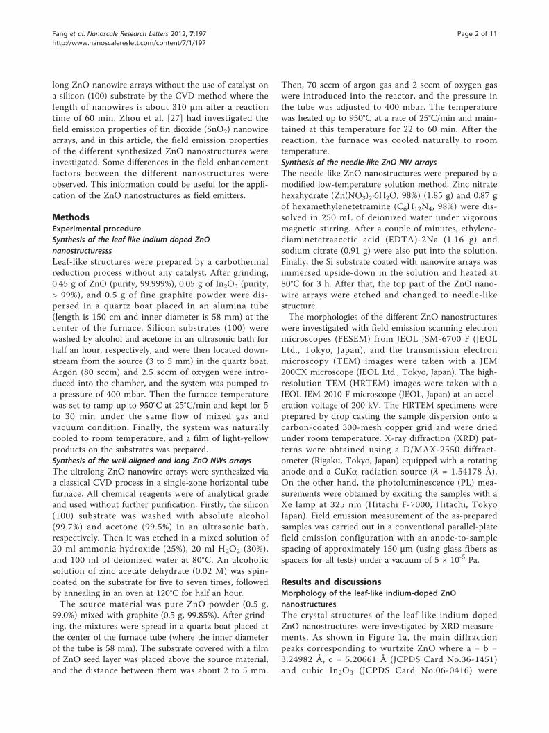
Results and discussionsMorphology of the leaf-like indium-doped ZnOnanostructuresThe crystal structures of the leaf-like indium-dopedZnO nanostructures were investigated by XRD measure-ments. As shown in Figure 1a, the main diffractionpeaks corresponding to wurtzite ZnO where a = b =3.24982 Å, c = 5.20661 Å (JCPDS Card No.36-1451)and cubic In2O3 (JCPDS Card No.06-0416) were
Fang et al. Nanoscale Research Letters 2012, 7:197http://www.nanoscalereslett.com/content/7/1/197
Page 2 of 11
observed in the spectrum. Figure 1a also shows that the(101,100) diffraction peaks are much stronger than theother peaks, which indicates that the {101} crystal facetsmay be the main growth plane of the as-prepared struc-tures. On the other hand, the SEM photographs of theindium-doped ZnO nanostructures in Figure 1b, c, dwere prepared with the reaction time of 5, 10, and 30min, respectively. The figure shows that, with increasingreaction time, the leaf-like structure becomes moreapparent where self-assembly flower-like structurescomposed of nanoparticles and nanobelts were observedon the seed layer as shown in Figure 1c at a longer reac-tion time of 10 min (initially in Figure 1b, the film con-sists of microparticles). The width and length of thebelt-like structures are around 300 to 600 nm and sev-eral micrometers, respectively, as shown in the figure.Finally, after a reaction time of 30 min, large-scale leaf-
like structures are self-assembled on the seed layers asshown in Figure 1d where the thickness of the leaf-likebranches is about 100 nm.In order to obtain more detail about the structures
and compositions of the leaf-like nanostructures,HRTEM, the fast Fourier transform (FFT), and selectedarea electron diffraction (SAED) measurements wereapplied for further characterization of the sample. Figure2a is the high-resolution TEM image of the area corre-sponding to the square area as shown in the inset ofFigure 2a where the brightfield and the darkfield imagescorrespond to the modulated structures of the In-dopedZnO and single-phase ZnO, respectively. On the otherhand, Zn, O, and Cu elements were both observed inthe energy dispersive X-ray spectroscopy (EDS) spec-trums corresponding to the darkfield (Figure 2c) andbrightfield (Figure 2d) parts, respectively. In addition,
Figure 1 Morphology of the leaf-like indium-doped ZnO nanostructures. (a) XRD pattern of the leaf-like indium-doped ZnO nanostructures.(b), (c), and (d) SEM images of the leaf-like nanostructures at different reaction times of 5, 10, and 30 min, respectively. The inset in (c) is a zoomof an SEM view of the leaf-like nanostructure, and the scale bar is 1 μm.
Fang et al. Nanoscale Research Letters 2012, 7:197http://www.nanoscalereslett.com/content/7/1/197
Page 3 of 11

the element indium was also observed in the brightfieldpart as shown in Figure 2d. On the other hand, the Cupeak is ascribed to the copper-coated TEM grid, and aclose value of molar ratio Zn and In is around 3.5:1 inthe brightfield part.As shown in Figure 2b, HRTEM image taken from the
junction between the brightfield and darkfield parts (Fig-ure 2a) indicates different lattice fringes of the modu-lated and single-phase structures, respectively. The FFTimage (Figure 2b) taken from the square marked ‘A’from the single lattice fringe shows that it is a typicalhexagonal structure consistent with wurtzite ZnO. Inaddition, the HRTEM image of this structure also showsthat the lattice spacing of 0.283 nm between adjacentlattice planes corresponds to the distance between two(10-10) crystal planes. The analysis of the HRTEM
image (the square A) agrees with the FFT pattern indi-cated by ‘a’. It is also demonstrated that the top andbottom surfaces of the leaf-like structures are the ±(0001) planes, and the growth orientation is along the a/b axis. On the other hand, the part marked ‘B’ lies atthe junction of the modulated structures and hexagonalZnO, which corresponds to FFT image ‘b’, and this partexhibits an approximate hexagonal structure. Conver-sely, the typically modulated structures taken in square‘C’ just accord with the result of the diffraction ‘c’ spots.It could be possibly due to the reason that the Zn sitesin the Zn-O slab are randomly replaced by the Inatoms, and hence, local lattice distortions are produced,which induce the periodic diffraction spots. As a result,the brightfield part of the leaf-like nanostructures seemsto be In-doped ZnO based. Moreover, the EDS
Figure 2 More detailed measurements of the leaf-like nanostructures. (a) TEM images of the brightfield and darkfield parts of the leaf-likenanostructures, and the inset is the TEM photograph of a small part of the leaf-like sample. (b) HRTEM image with which the insets in (b) arethe corresponding FFT images taken at the different square areas in the HRTEM image. EDS patterns (c) and (d) at the two circle regionscorresponding to the darkfield and brightfield regions, respectively, in the TEM image.
Fang et al. Nanoscale Research Letters 2012, 7:197http://www.nanoscalereslett.com/content/7/1/197
Page 4 of 11
spectrum in Figure 2d corresponding to the brightfieldregion indicates a higher intensity of the Zn element ascompared to the In element, and therefore, this furtherindicates that the leaf-like nanostructures are In-doped[28]. On the other hand, two sets (or series) of FFTdiffraction spots were observed (the first set is the seriesof slanted bright spots, and the second set is the seriesof fainter spots between the two slanted rows ofbright spots), as shown in the FFT image labeled as ‘c’in Figure 2b. These two different kinds of diffractionspots correspond to two parts of the discrepant crystallattices as observed in the FFT image c in Figure 2b.Figure 3 shows the HRTEM image of the modulated
structures in the brightfield part where the wide (bright)
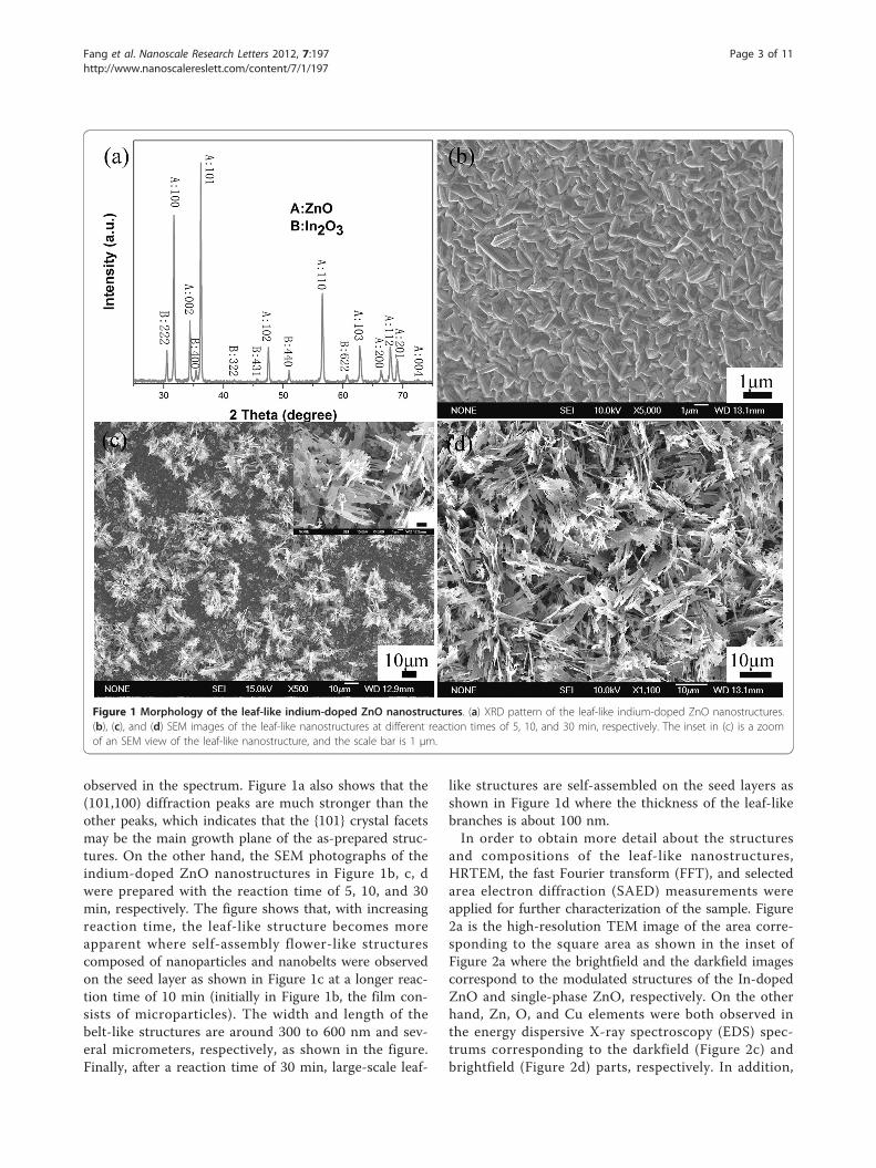
and narrow (bright) diagonal lines with a width of 0.283nm correspond to the In-O layers and In/Zn-O layers,respectively, where the growth direction of the In/Zn-Olayers is along the [10-10] direction (crystal ZnO growthdirection), as indicated in the figure [14]. However, dueto some significant changes to the structures of the leaf-like indium-doped ZnO nanostructures, the stackinglayers (bright wide crystal lattice lines) do not growalong the [10-10] orientation but at an angle about 30°,as indicated by the arrow in the HRTEM image and thecorresponding SAED pattern (inset of Figure 3). Theresults are different from previous reports [14]. In addi-tion, Figure 3 illustrates that each wide bright diagonalline corresponds to the In-O layers consist of about
Figure 3 HRTEM image of the superlattice structure. The inset of the figure shows the corresponding SAED pattern in the brightfield part ofthe leaf-like nanostructure.
Fang et al. Nanoscale Research Letters 2012, 7:197http://www.nanoscalereslett.com/content/7/1/197
Page 5 of 11
seven or eight In/Zn-O layers (width, 0.283 nm). On theother hand, the SAED pattern shows a series of parallellines and a number of small diffraction spots along thelines, which also indicates the presence of a modulatedstructure in the brightfield parts of the leaf-like nanos-tructure. For the In2O3(ZnO)m compounds, there is alinear relationship for the width, d of the In-O layer(wide bright diagonal line), given by [29]:
d = 6.349 + 2.602m A (1)
where m is the subscript in the chemical formula ofthe In2O3(ZnO)m compound.From the HRTEM image in Figure 3, the average
value of d is about 19 to 24 Ǻ (width of the bright diag-onal line), and hence, the value of m as calculated fromEquation 1 is between 7 to 8. Thus, the composition ofthe synthesized leaf-like structures in the brightfield partis estimated as In2O3(ZnO)7 or In2O3(ZnO)8. Theresults of the EDS spectrum are also applied to detectthe component ratios of Zn and In, which show a closevalue of the molar ratio of Zn:In at approximately 3.5:1or 4:1. Therefore, the darkfield part of our synthesizedleaf-like nanostructure is ZnO, and the brightfield partconsists of a modulated structure.
Growth mechanism of the leaf-like indium-doped ZnOnanostructuresThe growth mechanism of nanostructures is usuallyexplained by the vapor-liquid-solid (VLS) and vapor-solid (VS) processes where, according to the VLSgrowth mechanism, a droplet of the liquid alloy is akey role in reaction process, and hence, the VLSmechanism is also known as catalysis growth. In thiswork, catalyst was not used in the synthesis of thelarge-scale ZnO ‘leaf’ structures by the CVD route;hence, the VS mechanism is appropriate for the expla-nation of the growth process of the leaf-like indium-doped ZnO structures. In the VS mechanism, thenucleation probability is the critical factor for the for-mation of the 2-D structures. Based on the reactioncondition, the possible factors which could influencethe 2-D nucleation process can be expressed as fol-lows:
PN = B exp(− πσ 2
K2T2 ln α) (2)
where PN is the nucleation probability, B is a constant,s is the surface energy of the solid whisker, K is theBoltzmann constant, T is the absolute temperature inKelvin, a is the supersaturation ratio determined by a =p/po (and a is usually > 1), p is the actual vapor pres-sure, and po is the equilibrium vapor pressure corre-sponding to the temperature T.
According to Equation 2, the factors of s, a, and Teasily give rise to the 2-D nucleation where the highertemperature and larger supersaturation ratios canfacilitate the 2-D nucleation, thus further inducing theformation of the sheet-like structure [30]. Accordingto the above-analysis, the Si substrate in the furnaceis close to the source materials and lies at a zonewhere the temperature is high for the CVD process.Therefore, there is a higher distribution of vapor con-centration near the substrate. In the reaction process,with increasing reaction temperature, indium and zincvapor are generated by the carbothermal reduction ofIn2O3 and ZnO, respectively. Hence, a small binucleusstructure was first synthesized on the substrate by theZn and In mixture vapor atoms. With the increase ofreaction time, newly formed In/Zn atoms continue todeposit on the seed layer and result in the morpholo-gic evolvement from nanoparticles to belt-like and toleaf-like structures on the seed layer, respectively. Tokeep the system at a lower surface energy, the newarriving In/Zn atoms will react with the pumped-inoxygen gas and are adsorbed on the initial particle-like surfaces. Then, they tend to grow along the longi-tudinal and transverse growth directions at the sametime, which form belt-like structures as well as keepthe system at a lower surface energy. At the conditionwhere there is a combination of the high vapor con-centration and temperature, the Zn-In diphase will besupersaturated, and thus, the 2-D nucleation graduallyforms.As for the different lengths and widths of the leaf-like
branches, it is possible that there is some influence ofsome thermal or strain instability at the gas-solid inter-face state which does not involve much energy since thefree energy is the same for the equivalent {10-10} planes.In addition, the doped In atoms were obtained by theprocess of substituting the Zn atoms with the In atomsin the ZnO structures so that the system can be held ata lower energy [31]. By doping ZnO with In, the growthorientations of the resultant nanostructures varied fromthe highest-energy, low-index planes, and a fast growthalong [0001] to the sideway growth [10-10] directionwas observed [32,33]. In addition, the new arriving Inand Zn atoms in the vapor directly deposit on the sur-face of In-doped ZnO belt-like structure, and this directdeposition induces the growth of the side faces. There-fore, the seed layer self-assembles on the naked Si sub-strate and, thus, further induces the formation of leaf-like structures by epitaxial growth.
PL spectra of the leaf-like indium-doped ZnOnanostructuresFigure 4 shows the room temperature PL spectra forleaf-like (red line) indium-doped and wire-like (black
Fang et al. Nanoscale Research Letters 2012, 7:197http://www.nanoscalereslett.com/content/7/1/197
Page 6 of 11
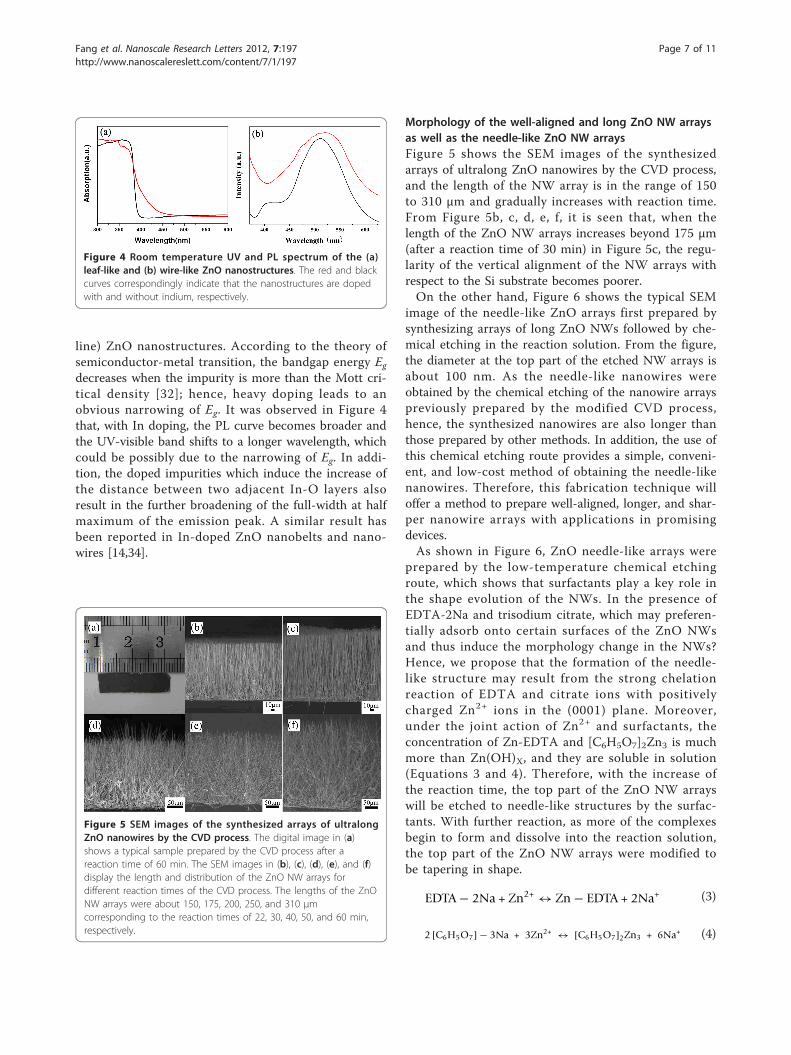
line) ZnO nanostructures. According to the theory ofsemiconductor-metal transition, the bandgap energy Egdecreases when the impurity is more than the Mott cri-tical density [32]; hence, heavy doping leads to anobvious narrowing of Eg. It was observed in Figure 4that, with In doping, the PL curve becomes broader andthe UV-visible band shifts to a longer wavelength, whichcould be possibly due to the narrowing of Eg. In addi-tion, the doped impurities which induce the increase ofthe distance between two adjacent In-O layers alsoresult in the further broadening of the full-width at halfmaximum of the emission peak. A similar result hasbeen reported in In-doped ZnO nanobelts and nano-wires [14,34].
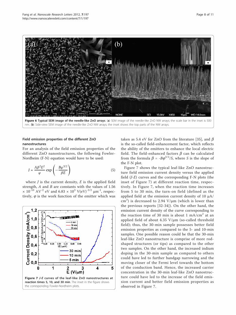
Morphology of the well-aligned and long ZnO NW arraysas well as the needle-like ZnO NW arraysFigure 5 shows the SEM images of the synthesizedarrays of ultralong ZnO nanowires by the CVD process,and the length of the NW array is in the range of 150to 310 μm and gradually increases with reaction time.From Figure 5b, c, d, e, f, it is seen that, when thelength of the ZnO NW arrays increases beyond 175 μm(after a reaction time of 30 min) in Figure 5c, the regu-larity of the vertical alignment of the NW arrays withrespect to the Si substrate becomes poorer.On the other hand, Figure 6 shows the typical SEM
image of the needle-like ZnO arrays first prepared bysynthesizing arrays of long ZnO NWs followed by che-mical etching in the reaction solution. From the figure,the diameter at the top part of the etched NW arrays isabout 100 nm. As the needle-like nanowires wereobtained by the chemical etching of the nanowire arrayspreviously prepared by the modified CVD process,hence, the synthesized nanowires are also longer thanthose prepared by other methods. In addition, the use ofthis chemical etching route provides a simple, conveni-ent, and low-cost method of obtaining the needle-likenanowires. Therefore, this fabrication technique willoffer a method to prepare well-aligned, longer, and shar-per nanowire arrays with applications in promisingdevices.As shown in Figure 6, ZnO needle-like arrays were
prepared by the low-temperature chemical etchingroute, which shows that surfactants play a key role inthe shape evolution of the NWs. In the presence ofEDTA-2Na and trisodium citrate, which may preferen-tially adsorb onto certain surfaces of the ZnO NWsand thus induce the morphology change in the NWs?Hence, we propose that the formation of the needle-like structure may result from the strong chelationreaction of EDTA and citrate ions with positivelycharged Zn2+ ions in the (0001) plane. Moreover,under the joint action of Zn2+ and surfactants, theconcentration of Zn-EDTA and [C6H5O7]2Zn3 is muchmore than Zn(OH)X, and they are soluble in solution(Equations 3 and 4). Therefore, with the increase ofthe reaction time, the top part of the ZnO NW arrayswill be etched to needle-like structures by the surfac-tants. With further reaction, as more of the complexesbegin to form and dissolve into the reaction solution,the top part of the ZnO NW arrays were modified tobe tapering in shape.
EDTA − 2Na + Zn2+ ↔ Zn − EDTA + 2Na+ (3)
2 [C6H5O7] − 3Na + 3Zn2+ ↔ [C6H5O7]2Zn3 + 6Na+ (4)
Figure 4 Room temperature UV and PL spectrum of the (a)leaf-like and (b) wire-like ZnO nanostructures. The red and blackcurves correspondingly indicate that the nanostructures are dopedwith and without indium, respectively.
Figure 5 SEM images of the synthesized arrays of ultralongZnO nanowires by the CVD process. The digital image in (a)shows a typical sample prepared by the CVD process after areaction time of 60 min. The SEM images in (b), (c), (d), (e), and (f)display the length and distribution of the ZnO NW arrays fordifferent reaction times of the CVD process. The lengths of the ZnONW arrays were about 150, 175, 200, 250, and 310 μmcorresponding to the reaction times of 22, 30, 40, 50, and 60 min,respectively.
Fang et al. Nanoscale Research Letters 2012, 7:197http://www.nanoscalereslett.com/content/7/1/197
Page 7 of 11
Field emission properties of the different ZnOnanostructuresFor an analysis of the field emission properties of thedifferent ZnO nanostructures, the following Fowler-Nordheim (F-N) equation would have to be used:
J =Aβ2E2
ϕexp
(−Bϕ3/2
βE
)(5)
where J is the current density, E is the applied fieldstrength, A and B are constants with the values of 1.56× 10⁻¹⁰ AV-2 eV and 6.83 × 10³ V(eV)-3/2 μm-1, respec-tively, j is the work function of the emitter which was
taken as 5.4 eV for ZnO from the literature [35], and bis the so-called field-enhancement factor, which reflectsthe ability of the emitters to enhance the local electricfield. The field-enhanced factors b can be calculatedfrom the formula b = -Bj3/2/S, where S is the slope ofthe F-N plot.Figure 7 shows the typical leaf-like ZnO nanostruc-
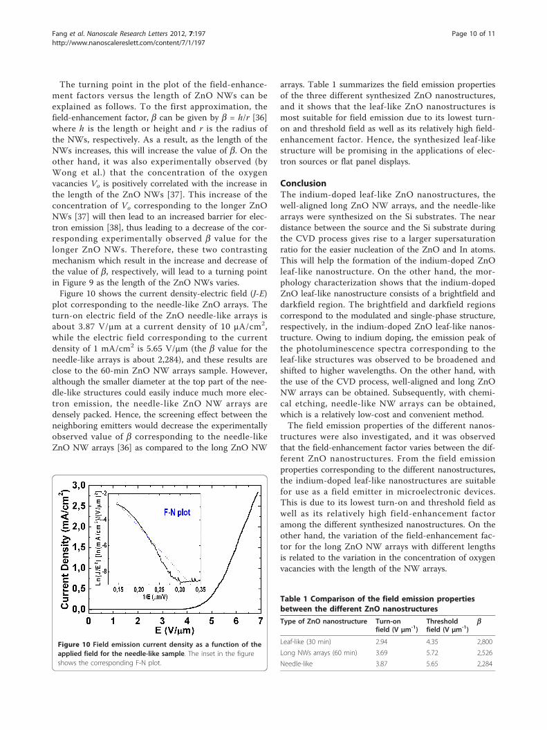
ture field emission current density versus the appliedfield (J-E) curves and the corresponding F-N plots (theinset of Figure 7) at different reaction time, respec-tively. In Figure 7, when the reaction time increasesfrom 5 to 30 min, the turn-on field (defined as theapplied field at the emission current density of 10 μA/cm2) is decreased to 2.94 V/μm (which is lower thanthe previous reports [32-34]). On the other hand, theemission current density of the curve corresponding tothe reaction time of 30 min is about 1 mA/cm2 at anapplied field of about 4.35 V/μm (so-called thresholdfield); thus, the 30-min sample possesses better fieldemission properties as compared to the 5- and 10-minsamples. One possible reason could be that the 30-minleaf-like ZnO nanostructure is comprise of more rod-shaped structures (or tips) as compared to the othertwo samples. On the other hand, the increased indiumdoping in the 30-min sample as compared to otherscould have led to further bandgap narrowing and themoving closer of the Fermi level towards the bottomof the conduction band. Hence, the increased carrierconcentration in the 30-min leaf-like ZnO nanostruc-ture could have led to the increase of the field emis-sion current and better field emission properties asobserved in Figure 7.
Figure 6 Typical SEM image of the needle-like ZnO arrays. (a) SEM image of the needle-like ZnO NW arrays; the scale bar in the inset is 500nm. (b) Side-view SEM image of the needle-like ZnO NW arrays; the inset shows the top parts of the NW arrays.
Figure 7 J-E curves of the leaf-like ZnO nanostructures atreaction times 5, 10, and 30 min. The inset in the figure showsthe corresponding Fowler-Nordheim plots.
Fang et al. Nanoscale Research Letters 2012, 7:197http://www.nanoscalereslett.com/content/7/1/197
Page 8 of 11

Based on Equation 5, the experimental b value forboth the 30- and 10-min leaf-like ZnO nanostructuresamples are close to 2,800. Conversely for the 5-minsample, the corresponding J-E curve in Figure 7 isobserved to be nonlinear, and it could be possibly dueto the reason that the sample consists of microparticles,thus leading to a relatively high turn-on field and a non-linear relationship.On the other hand, Figures 8 and 9 show the plot of
the emission current density versus the electric field ofthe long ZnO nanowire arrays at different reaction
time (during the CVD process) and their correspond-ing field-enhancement factors, respectively. In Figure 8,when the reaction time increases from 22 to 60 min,the turn-on field (defined as the applied field at theemission current density of 10 μA/cm2) decreases from4.56 to 3.69 V/μm, respectively. In addition, the emis-sion current density of the curves also decreases from7.09 to 5.72 μA/cm2 at the threshold field. Hence, the60-min sample possesses better field emission proper-ties as compared to the others (22- to 50-min sam-ples). Based on the formula in Equation 5, theexperimental b values for the 22- to 60-min samplesare plotted in Figure 9. Comparing the experimental bvalue between the indium-doped leaf-like ZnO nanos-tructures and the long ZnO NW arrays, it was seenthat the 30-min indium-doped leaf-like nanostructurespossess a slightly higher b value as compared to mostof the long ZnO NW array samples (except for the 22-min sample whose average length of the NWs is about150 μm in Figure 9).It is well-known that the field emission properties of
the 1-D nanostructures depend on the tip morphology,density, and the aspect ratio of the length to diameter(h/d) corresponding to the NWs [36]. Although the longZnO NW arrays have a relatively bigger diameter, theirhigher aspect ratios, however, would help to improvethe field-enhancement factors. Nonlinearity is alsoobserved in the F-N plots corresponding to the 22- to60-min samples, which could be possibly due to thehigh density of the NW arrays in the samples.
Figure 8 J-E curves of the long ZnO nanowire arrays atdifferent reaction times.
Figure 9 Field-enhanced factors of the long ZnO NW arrays of different length.
Fang et al. Nanoscale Research Letters 2012, 7:197http://www.nanoscalereslett.com/content/7/1/197
Page 9 of 11
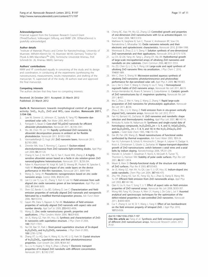
The turning point in the plot of the field-enhance-ment factors versus the length of ZnO NWs can beexplained as follows. To the first approximation, thefield-enhancement factor, b can be given by b = h/r [36]where h is the length or height and r is the radius ofthe NWs, respectively. As a result, as the length of theNWs increases, this will increase the value of b. On theother hand, it was also experimentally observed (byWong et al.) that the concentration of the oxygenvacancies Vo is positively correlated with the increase inthe length of the ZnO NWs [37]. This increase of theconcentration of Vo corresponding to the longer ZnONWs [37] will then lead to an increased barrier for elec-tron emission [38], thus leading to a decrease of the cor-responding experimentally observed b value for thelonger ZnO NWs. Therefore, these two contrastingmechanism which result in the increase and decrease ofthe value of b, respectively, will lead to a turning pointin Figure 9 as the length of the ZnO NWs varies.Figure 10 shows the current density-electric field (J-E)
plot corresponding to the needle-like ZnO arrays. Theturn-on electric field of the ZnO needle-like arrays isabout 3.87 V/μm at a current density of 10 μA/cm2,while the electric field corresponding to the currentdensity of 1 mA/cm2 is 5.65 V/μm (the b value for theneedle-like arrays is about 2,284), and these results areclose to the 60-min ZnO NW arrays sample. However,although the smaller diameter at the top part of the nee-dle-like structures could easily induce much more elec-tron emission, the needle-like ZnO NW arrays aredensely packed. Hence, the screening effect between theneighboring emitters would decrease the experimentallyobserved value of b corresponding to the needle-likeZnO NW arrays [36] as compared to the long ZnO NW
arrays. Table 1 summarizes the field emission propertiesof the three different synthesized ZnO nanostructures,and it shows that the leaf-like ZnO nanostructures ismost suitable for field emission due to its lowest turn-on and threshold field as well as its relatively high field-enhancement factor. Hence, the synthesized leaf-likestructure will be promising in the applications of elec-tron sources or flat panel displays.
ConclusionThe indium-doped leaf-like ZnO nanostructures, thewell-aligned long ZnO NW arrays, and the needle-likearrays were synthesized on the Si substrates. The neardistance between the source and the Si substrate duringthe CVD process gives rise to a larger supersaturationratio for the easier nucleation of the ZnO and In atoms.This will help the formation of the indium-doped ZnOleaf-like nanostructure. On the other hand, the mor-phology characterization shows that the indium-dopedZnO leaf-like nanostructure consists of a brightfield anddarkfield region. The brightfield and darkfield regionscorrespond to the modulated and single-phase structure,respectively, in the indium-doped ZnO leaf-like nanos-tructure. Owing to indium doping, the emission peak ofthe photoluminescence spectra corresponding to theleaf-like structures was observed to be broadened andshifted to higher wavelengths. On the other hand, withthe use of the CVD process, well-aligned and long ZnONW arrays can be obtained. Subsequently, with chemi-cal etching, needle-like NW arrays can be obtained,which is a relatively low-cost and convenient method.The field emission properties of the different nanos-
tructures were also investigated, and it was observedthat the field-enhancement factor varies between the dif-ferent ZnO nanostructures. From the field emissionproperties corresponding to the different nanostructures,the indium-doped leaf-like nanostructures are suitablefor use as a field emitter in microelectronic devices.This is due to its lowest turn-on and threshold field aswell as its relatively high field-enhancement factoramong the different synthesized nanostructures. On theother hand, the variation of the field-enhancement fac-tor for the long ZnO NW arrays with different lengthsis related to the variation in the concentration of oxygenvacancies with the length of the NW arrays.
Figure 10 Field emission current density as a function of theapplied field for the needle-like sample. The inset in the figureshows the corresponding F-N plot.
Table 1 Comparison of the field emission propertiesbetween the different ZnO nanostructures
Type of ZnO nanostructure Turn-onfield (V μm-1)
Thresholdfield (V μm-1)
b
Leaf-like (30 min) 2.94 4.35 2,800
Long NWs arrays (60 min) 3.69 5.72 2,526
Needle-like 3.87 5.65 2,284
Fang et al. Nanoscale Research Letters 2012, 7:197http://www.nanoscalereslett.com/content/7/1/197
Page 10 of 11
AcknowledgementsFinancial support from the European Research Council Grant(ThreeDSurface), Volkswagen Stiftung, and BMBF (ZIK: 3DNanoDevice) isgratefully acknowledged.
Author details1Institute of Materials Physics and Center for Nanotechnology, University ofMuenster, Wilhelm-Klemm-Str. 10, Muenster 48149, Germany 2Institut fürPhysik & IMN MacroNano®® (ZIK), Technische Universität Ilmenau, Prof.Schmidt-Str. 26, Ilmenau 98693, Germany
Authors’ contributionsKMW and YF contributed equally in conceiving of the study and its designand coordination, in conducting all the experiments (synthesizing thenanostructures), measurements, results interpretation, and drafting of themanuscript. YL supervised all of the study. All authors read and approvedthe final manuscript.
Competing interestsThe authors declare that they have no competing interests.
Received: 26 October 2011 Accepted: 23 March 2012Published: 23 March 2012
Gurlo A: Nanosensors: towards morphological control of gas sensingactivity. SnO2, In2O3, ZnO and WO3 case studies. Nanoscale 2011,3:154-156.2. Law M, Greene LE, Johinson JC, Saykally R, Yang PD: Nanowire dye-
sensitized solar cells. Nat Mater 2005, 4:455-459.3. Panigrahi S, Basak D: Core-shell TiO2@ZnO nanorods for efficient
ultraviolet photodetection. Nanoscale 2011, 3:2336-2341.4. Wu JM, Chen YR, Lin YH: Rapidly synthesized ZnO nanowires by
ultraviolet decomposition process in ambient air for flexiblephotodetector. Nanoscale 2011, 3:1053-1058.
5. Vanmaekelbergh D, Vugt LKV: ZnO nanowire lasers. Nanoscale 2011,3:2783-2800.
6. Zimmler MA, Voss T, Ronning C, Capasso F: Exciton-relatedelectroluminescence from ZnO nanowire light-emitting diodes. Appl PhysLett 2009, 94:241120.
7. Chang H, Sun Z, Ho KYF, Tao X, Yan F, Kwok WM, Zheng Z: A highlysensitive ultraviolet sensor based on a facile in situ solution-grown ZnOnanorod/graphene heterostructure. Nanoscale 2011, 3:258-264.
8. Faber H, Klaumünzer M, Voigt M, Galli D, Vieweg BF, Peukert W, Spiecker E,Halik M: Morphological impact of zinc oxide layers on the deviceperformance in thin-film transistors. Nanoscale 2011, 3:897-899.
9. Wang ZL, Song JH: Piezoelectric nanogenerators based on zinc oxidenanowire arrays. Science 2006, 312:242-245.
10. Lee CJ, Lee TJ, Lyu SC, Zhang Y, Ruh H, Lee HJ: Field emission from well-aligned zinc oxide nanowires grown at low temperature. Appl Phys Lett2002, 81:3648-3650.
11. Shen GZ, Bando Y, Liu BD, Golberg D, Lee C: Characterization and field-emission properties of vertically aligned ZnO nanonails and nanopencilsfabricated by a modified thermal-evaporation process. Adv Funct Mater2006, 16:410-416.
12. Gayen RN, Dalui S, Rajaram A, Pal AK: Modulation of field emissionproperties of vertically aligned ZnO nanorods with aspect ratio andnumber density. Appl Surf Sci 2009, 255:4902-4906.
13. Wang ZL: Zinc oxide nanostructures: growth, properties andapplications. J Phys Condens Matter 2004, 16:829-858.
14. Jie JS, Wang GZ, Han XH, Hou JG: Synthesis and characterization of ZnO:In nanowires with superlattice structure. J Phys Chem B 2004,108:17027-17031.
15. Na CW, Bae SY, Park J: Short-period superlattice structure of Sn-dopedIn2O3(ZnO)4 and In2O3(ZnO)5 nanowires. J Phys Chem B 2005,109:12785-12790.
16. Zhang XT, Lu HQ, Gao H, Wang XJ, Xu HY, Li Q, Hark SK: Crystal structureof In2O3(ZnO)m superlattice wires and their photoluminescenceproperties. Cryst Growth Des 2009, 9:364-367.
17. Su J, Li H, Huang Y, Xing X, Zhao J, Zhang Y: Electronic transportproperties of In-doped ZnO nanobelts with different concentration.Nanoscale 2011, 3:2182-2187.
18. Cheng BC, Xiao YH, Wu GS, Zhang LD: Controlled growth and propertiesof one-dimension ZnO nanostructures with Ce as activator/dopant. AdvFunct Mater 2004, 14:913-919.
19. Mathews N, Varghese B, Sun C, Thavasi V, Andreasson BP, Sow CH,Ramakrishna S, Mhaisalkar SG: Oxide nanowire networks and theirelectronic and optoelectronic characteristics. Nanoscale 2010, 2:1984-1998.
20. Weintraub B, Zhou Z, Li Y, Deng Y: Solution synthesis of one-dimensionalZnO nanomaterials and their applications. Nanoscale 2010, 2:1573-1578.
21. Lu CH, Qi LM, Yang JH, Tang L, Zhang DY, Ma JM: Hydrothermal growthof large-scale micropatterned arrays of ultralong ZnO nanowires andnanobelts on zinc substrate. Chem Commun 2006, 42:3551-3553.
22. Hu ZD, Chen Q, Li Z, Yu Y, Peng LM: Large-scale and rapid synthesis ofultralong ZnO nanowire films via anodization. J Phys Chem C 2010,114:881-889.
23. Min C, Shen X, Sheng W: Microwave-assisted aqueous synthesis ofultralong ZnO nanowires: photoluminescence and photovoltaicperformance for dye-sensitized solar cell. Appl Phys A 2009, 96:799-803.
24. Liu J, Xie S, Chen Y, Wang X, Cheng H, Liu F, Yang J: Homoepitaxialregrowth habits of ZnO nanowire arrays. Nanoscale Res Lett 2011, 6:619.
25. Arroyo-Hernández M, Álvaro R, Serrano S, Costa-Krämer JL: Catalytic growthof ZnO nanostructures by r.f. magnetron sputtering. Nanoscale Res Lett2011, 6:437.
26. Ma C, Zhou Z, Wei H, Yang Z, Wang Z, Zhang Y: Rapid large-scalepreparation of ZnO nanowires for photocatalytic application. NanoscaleRes Lett 2011, 6:536.
27. Zhou Z, Wu J, Li H, Wang Z: Field emission from in situ-grown verticallyaligned SnO2 nanowire arrays. Nanoscale Res Lett 2012, 7:117.
28. Fan HJ, Barnard AS, Zacharias M: ZnO nanowires and nanobelts: shapeselection and thermodynamic modeling. Appl Phys Lett 2007, 90:143116.
29. Kimizuka N, Isobe M, Nakamura M: Syntheses and single-crystal data ofhomologous compounds, In2O3(ZnO)m(m = 3, 4, and 5), InGaO3(ZnO)3,and Ga2O3(ZnO)m (m = 7, 8, 9, and 16) in the In2O3-ZnGa2O4-ZnOsystem. J Solid State Chem 1995, 116:170-178.
30. Dai ZR, Pan ZW, Wang ZL: Novel nanostructures of functional oxidessynthesized by thermal evaporation. Adv Funct Mater 2003, 13:9-24.
31. Fan HJ, Fuhrmann B, Scholz R, Himcinschi C, Berger A, Leipner H, Dadgar A,Krost A, Christiansen S, Gösele U, Zacharias M: Vapour-transport-depositiongrowth of ZnO nanostructures: switch between c-axial wires and a-axialbelts by indium doping. Nanotechnology 2006, 17:231-239.
32. Wander A, Schedin F, Steadman P, Norris A, McGrath R, Turner TS,Thornton G, Harrison NM: Stability of polar oxide surfaces. Phys Rev Lett2001, 86:3811-3814.
33. Meyer B, Marx D: Density-functional study of the structure and stabilityof ZnO surfaces. Phys Rev B 2003, 67:035403.
34. Jie JS, Wang GZ, Han XH, Yu QX, Liao Y, Li GP, Hou JG: Indium-doped zincoxide nanobelts. Chem Phys Lett 2004, 387:466-470.
35. Zhu YW, Zhang HZ, Sun XC, Feng SQ, Xu J, Zhao Q, Xiang B, Wang RM,Yu DP: Efficient field emission from ZnO nanoneedle arrays. Appl PhysLett 2003, 83:144-146.
36. Qian X, Liu H, Guo Y, Song Y, Li Y: Effect of aspect ratio on field emissionproperties of ZnO nanorod arrays. Nanoscale Res Lett 2008, 3:303-307.
37. Wong KM, Fang YG, Devaux A, Wen LY, Huang J, De Cola L, Lei Y: Assortedanalytical and spectroscopic techniques for the optimization of thedefect-related properties in size-controlled ZnO nanowires. Nanoscale2011, 3:4830-4839.
38. Cui Y, Zhang X, Lei W, Di Y, Wang J, Yang X: Effect of ion bombardmenton the field emission property of tetrapod ZnO. J Appl Phys 2010,107:054506.
doi:10.1186/1556-276X-7-197Cite this article as: Fang et al.: Synthesis and field emission propertiesof different ZnO nanostructure arrays. Nanoscale Research Letters 20127:197.
Fang et al. Nanoscale Research Letters 2012, 7:197http://www.nanoscalereslett.com/content/7/1/197
Page 11 of 11