Embed Size (px)
Citation preview
19
Synchrotron Radiation Gwyn P. Williams
National Synchrotron Light Source, Brookhaven National Laboratory

20
21
Synchrotron Radiation Gwyn P. Williams
National Synchrotron Light Source, Brookhaven National Laboratory
Today synchrotron radiation is used for a number of applications. The National Synchrotron Light Source at Brookhaven National Laboratory (BNL) serves the needs of a large spectrum of university and industrial users. The range of applications covers such diverse subjects as catalysis and corrosion. Here I'll concentrate on x-ray lithography, which is an especially interesting application. A fascinating sidelight of this application is the production of commercial accelerators for x-ray lithography.
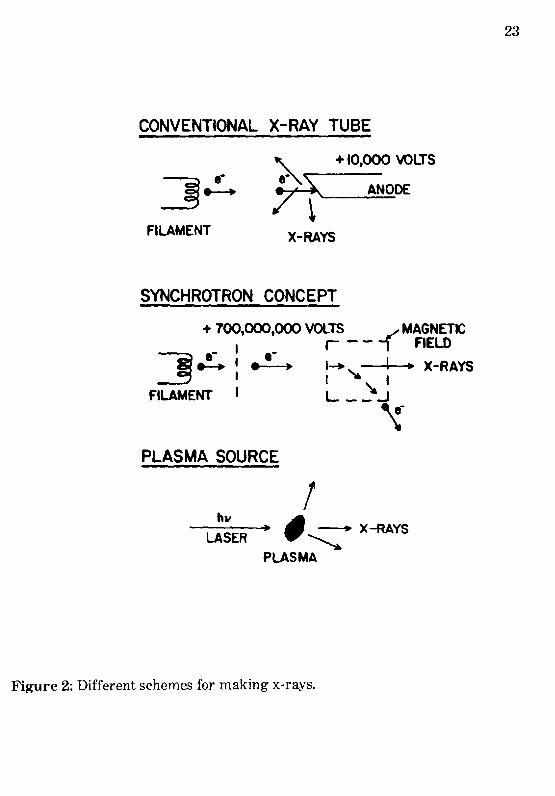
Synchrotron radiation is synonymous with x-rays. From the initial invention of the x-ray tube in 1896 until about 1960, the brightness (the log of brilliance in Fig. 1) didn't change very much. About that time rotating anode tubes appeared. Then, starting in the Sixties, synchrotron radiation facilities began popping up. They appeared at Madison and Stanford and at various places in Europe, including England, where I became involved about 20 years ago. Soon, these accelerator x-ray sources produced dramatic increases in the x-ray brightness until they are now a trillion times brighter than a conventional x-ray machine. When a charged particle accelerates it radiates photons or x-rays. For example, in a conventional x-ray tube the electron beam accelerates from a filament to an anode, where it decelerates rapidly at the anode and emits x-rays (shown schematically in Fig. 2).
A different approach is to accelerate (or decelerate) the particle by passing it through a magnetic field. This is what really happens in an accelerator. When the particles curve in the magnetic field, x-rays are emitted. These x-rays are very collimated. The effective source is very small because the electrons can be focused down. There's also no heating involved, so it's possible to make an extremely bright source of x-rays. This is the essence of synchrotron radiation.
The Tevatron at Fermilab uses protons. It's much harder to make an accelerator like the Tevatron for electrons because electrons radiate much more as
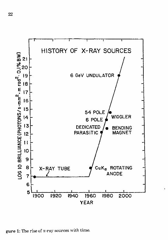
22
- HiSTORY OF X-RAY SOURCES ~ 21 o ~20 o
N° 19 6 GeV UNDULATOR "'CI
~18
~ 17 N
~ 16. en 15..... 54 POLE.en
6 POLE WIGGLER
b 13
5 14
DEDICATED • BENDING:r: PARASITIC MAGNET!:; 12
w ~II ~
:J 10 -J
g§ 9
o 8 X- RAY TUBE CuKa ROTATING ANODE§ 7 r-.--...::;/-----~
6
5 1900 1920 1940 1960 1980 2000 YEAR
\Plre 1: The rise of x-ray sources with time.
23
CONVENTIONAL X-RAY TUBE
~ + 10,000 WLTS
7'f ANODE
FILAMENT X-RAYS
SYNCHROTRON CONCEPT
.+ 700,000,000 VOlTS ,/' MAGNETIC
r -- -, FIELDI 1.....-.. 1-+...... I ~ X-RAYS~~ I I .. I
FILAMENT I L_~..J'\PLASMA SOURCE
! hI'----+. , - X-RAYS
LASER ........... PLASMA
Figure 2: Different schemes for making x-rays.
24
they go around a circle. As a result, it is difficult to put enough power in to keep a beam in the storage ring. A proton is 2000 times heavier than an electron. Emission of x-rays goes as the inverse fourth power of the mass. As a result, protons don't radiate nearly as much synchrotron radiation. Actually, that's why very high-energy machines like the Tevatron use protons.
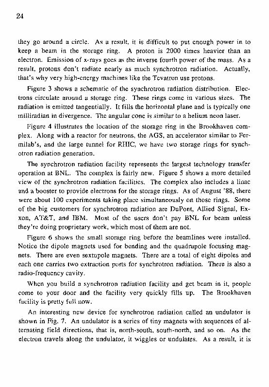
Figure 3 shows a schematic of the synchrotron radiation distribution. Electrons circulate around a storage ring. These rings come in various sizes. The radiation is emitted tangentially. It fills the horizontal plane and is typically one milliradian in divergence. The angular cone is similar to a helium neon laser.
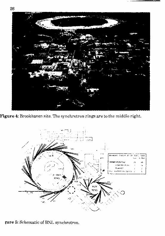
Figure 4 illustrates the location of the storage ring in the Brookhaven complex. Along with a reactor for neutrons, the AGS, an accelerator similar to Fermilab's, and the large tunnel for RHIC, we have two storage rings for synchotron radiation generation.
The synchrotron radiation facility represents the largest technology transfer operation at BNL. The complex is fairly new. Figure 5 shows a more detailed view of the synchrotron radiation facilities. The complex also includes a linac and a booster to provide electrons for the storage rings. As of August '88, there were about 100 experiments taking place simultaneously on those rings. Some of the big customers for synchrotron radiation are DuPont, Allied Signal, Exxon, AT&T, and IBM. Most of the users don't pay BNL for beam unless they're doing proprietary work, which most of them are not.
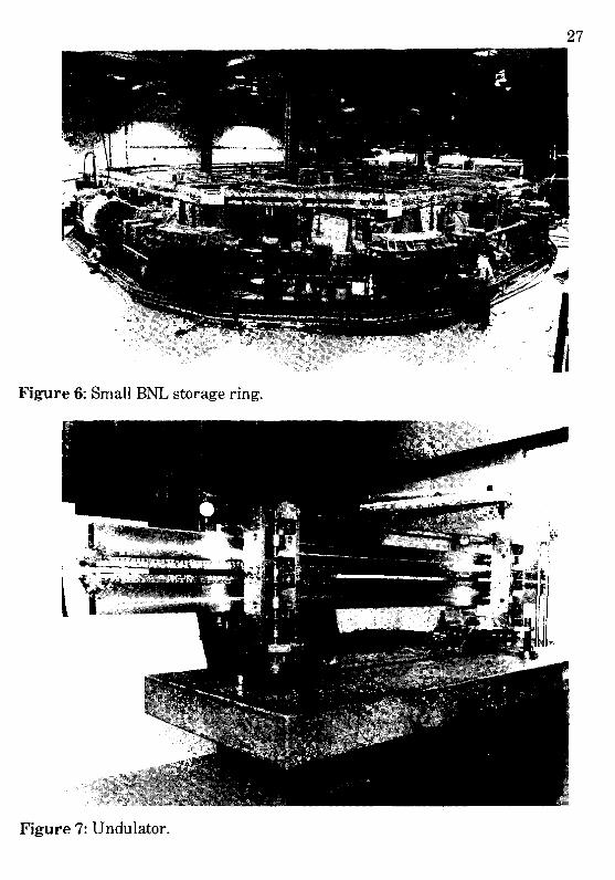
Figure 6 shows the small storage ring before the beamlines were installed. Notice the dipole magnets used for bending and the quadrupole focusing magnets. There are even sextupole magnets. There are a total of eight dipoles and each one carries two extraction ports for synchrotron radiation. There is also a radio-frequency cavity.
When you build a synchrotron radiation facility and get beam in it, people come to your door and the facility very quickly fills up. The Brookhaven facili ty is pretty full now.
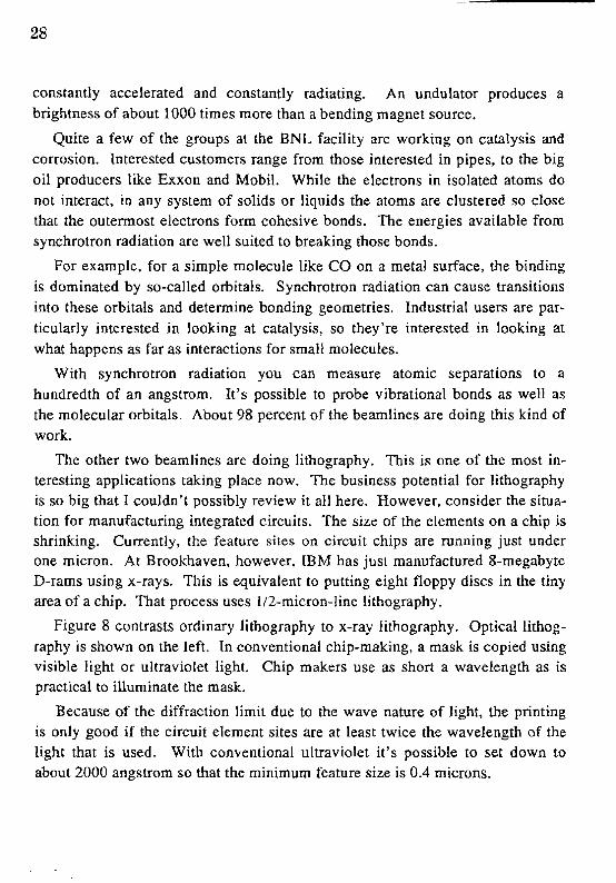
An interesting new device for synchrotron radiation called an undulator is shown in Fig. 7. An undulator is a series of tiny magnets with sequences of alternating field directions, that is, north-south, south-north, and so on. As the electron travels along the undulator, it wiggles or undulates. As a result, it is
25
electron orbit--.......e\ectron orbif--.,~- acc. .....
Figure 3: Synchrotron radiation distribution.
26
Figure 4: Brookhaven site. The synchrotron rings are to the middle right.
-OPt.:RA,TiNG
8[AMLlN( SlAWS o1S OI ~~!:f'\ 1989 y",,, )",R,Ili
29
Plre 5: Schematic of BNL synchrotron.
27
Figure 6: Small BNL storage ring.
Figure 7: Undulator.
28
constantly accelerated and constantly radiating. An undulator produces a brightness of about 1000 times more than a bending magnet source.
Quite a few of the groups at the BNL facility are working on catalysis and corrosion. Interested customers range from those interested in pipes, to the big oil producers like Exxon and Mobil. While the electrons in isolated atoms do not interact, in any system of solids or liquids the atoms are clustered so close that the outermost electrons form cohesive bonds. The energies available from synchrotron radiation are well suited to breaking those bonds.
For example, for a simple molecule like CO on a metal surface, the binding is dominated by so-called orbitals. Synchrotron radiation can cause transitions into these orbitals and determine bonding geometries. Industrial users are particularly interested in looking at catalysis, so they're interested in looking at what happens as far as interactions for small molecules.
With synchrotron radiation you can measure atomic separations to a hundredth of an angstrom. It's possible to probe vibrational bonds as well as the molecular orbitals. About 98 percent of the beamlines are doing this kind of work.
The other two beamlines are doing lithography. This is one of the most interesting applications taking place now. The business potential for lithography is so big that I couldn't possibly review it all here. However, consider the situation for manufacturing integrated circuits. The size of the elements on a chip is shrinking. Currently, the feature sites on circuit chips are running just under one micron. At Brookhaven, however, IBM has just manufactured 8-megabyte D-rams using x-rays. This is equivalent to putting eight floppy discs in the tiny area of a chip. That process uses 1I2-micron-line lithography.
Figure 8 contrasts ordinary lithography to x-ray lithography. Opticallithography is shown on the left. In conventional chip-making, a mask is copied using visible light or ultraviolet light. Chip makers use as short a wavelength as is practical to illuminate the mask.
Because of the diffraction limit due to the wave nature of light, the printing is only good if the circuit element sites are at least twice the wavelength of the light that is used. With conventional ultraviolet it's possible to set down to about 2000 angstrom so that the minimum feature size is 0.4 microns.

29 .
Wafer Optical Lithography
CC=:=:=:=====::JI Wafer
x-Ray Lithography
Figure 8: Comparison of optical and x-ray lithography.
30
Why isn't it possible to just go a little bit further into the ultraviolet? It turns out it is difficult to make lenses and there aren't any suitable window materials. The problem is that everything absorbs like crazy. The best solution is to jump several orders of magnitude, down to 10 angstroms. With lO-angstrom x-rays, it's only necessary to take a mask and just do a contact print. These dimensions can be as small as 100 angstroms and one still gets perfect printing.
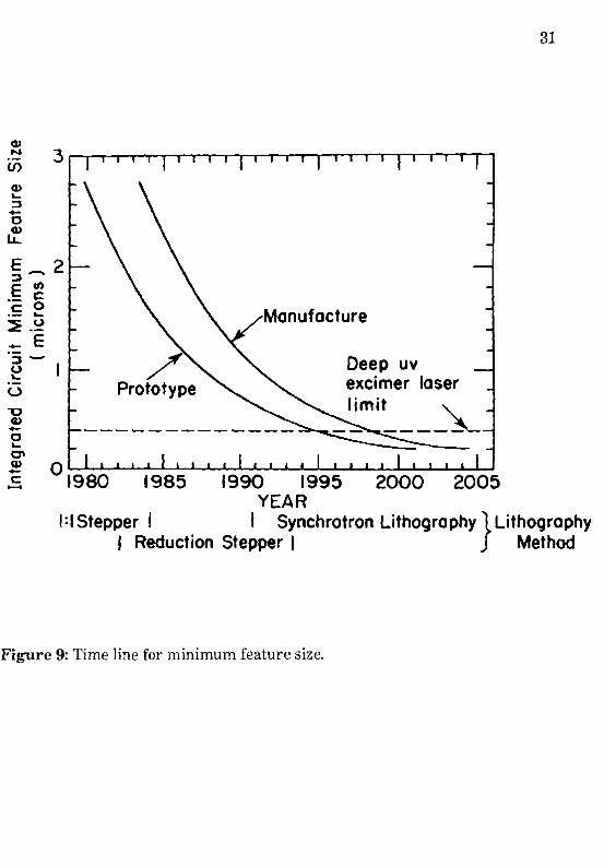
Sub-micron lithography has now become very big business. Figure 9 shows the time line for requirements on integrated circuit minimum feature size in microns. One curve is for prototypes, and the other for manufacture. The horizontal line is the deep ultraviolet diffraction limit.
In effect, it's not possible to print smaller than that using a laser. There is also a lot of evidence that synchrotron lithography will actually beat optical lithography on price by a factor of two or even better. This would be a huge effect.
As a result, at some point in the early 1990s the integrated circuit business will be forced to get into synchrotron lithography.
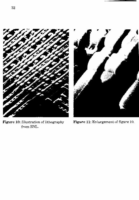
The next few figures show some of the images made at Brookhaven using xray lithography.
The current setup at Brookhaven is a facility in which there is a ring with eight magnets, a clean room, and an oscillating mirror. IBM is our collaborator in this. Obviously, they are in the world's forefront in chip manufacturing.
This year, IBM has also set up a manufacturing facility at Brookhaven. Figure 10 shows an illustration from that line. Figure 11 is an enlargement. The detail where the 112-micron lines cross is quite fantastic compared to anything done optically. Optical lithography would have a hard time producing these images.
These line widths are compatible with making a 64-megabyte D-ram. IBM is just getting set up to produce them.
The synchrotron x-ray technique is very insensitive to defects and also insensitive to dust. If there is dust, the x-rays print right through it. The technique also has fantastic process latitude, that is, it's quite difficult to overexpose. You can overexpose by 150 percent, or 100 percent, and the lines are still perfect.
31
0 1980 1985 1990 1995 2000 2005 YEAR
1;1 Stepper I I Synchrotron lithOgraPhY} Lithography I Reduction Stepper I Method
Figure 9: Time line for minimum feature size.
Q) N
U> Q) .... ~
+o ~
E_2 ::JE C/)._ c c 0.- ...
::1E .~ +- E :Je u "0 cu +o.... C'l cu +c:-
Deep uv excimer laser limit
32
Figure 10: Illustration of lithography Figure 11: Enlargement of figure 10. fromBNL.
33
Many analysts predict this will be an enormous business. On the other hand, companies don't want to come to Brookhaven and work on a big accelerator. They would like to have a small superconducting ring with various exposure
stations on it.
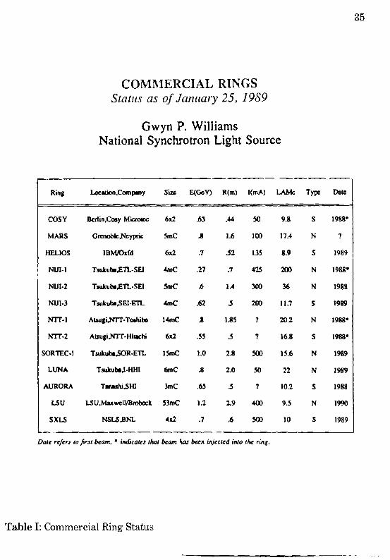
IBM has ordered a compact electron storage ring. Oxford Instruments is manufacturing it. Brookhaven has held several technology transfer workshops on this topic. Table I lists the world efforts in this field. Some of the groups, such as the French, have now dropped out, but a new Russian group has entered
the fray.
At present, about 12 groups are producing small, compact rings, including the Grumman team that is building the IBM machine in collaboration with Gen
eral Dynamics.
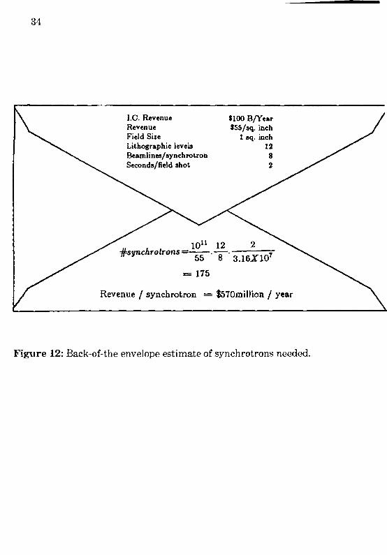
Figure 12 is a revenue estimate from AT&T by Arnie Yanof. Assume all the chips have to be made by x-ray lithography and it's a $100 billion-a-year market with a $55 per square-inch revenue. With a 1 square-inch field size, 12 lithographic levels, 8 beamlines per synchrotron, and 2 seconds for field shot, the number of synchrotrons needed is 175, just for lithography. Each ring would produce a revenue of $570 million per year.
We haven't even discussed other applications of synchrotron radiation. Several others are quite interesting. One example is x-ray microscopy. The resolution is not as high as electron microscopy. On the other hand, it's possible to look at wet, living biological specimens with a resolution that is currently about 300 angstroms.
Another interesting application with synchrotron radiation is coronary angiography, taking images of the heart. It's possible to take millisecond flash pictures of blood vessels in the heart. This is another program under way at Brookhaven.
A third possibility I discussed earlier was catalysis and corrosion analysis. This is also a huge field.
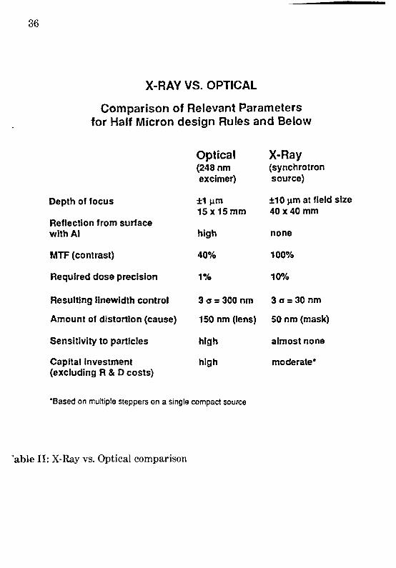
Table II shows a comparison of x-ray and electron (or e-beam) lithography, prepared by IBM. Some people ask why use x-rays, why not just use an electron or e-beam? Also, as far as x-ray sources are concerned, there are plasma
34
I.C. Revenue SIOO BfYear Revenue 'SS/sq. incb Field Size 1 sq. incb Lithographic levela 12 Beamlines/synchrotron 8 Seconds/field shot 2
1011 12 2 #synchrolrons==SS'S' 3.16X107
= 175
Revenue I synchrotron = $570million I year
Figure 12: Back-oi-the envelope estimate of synchrotrons needed.
35
COMMERCIAL RINGS Slaws as of January 25, 1989
Gwyn p, Williams National Synchrotron Light Source
Ring LocIllion.ComI*lY Size E(GeV) R(m) l(mA) LAMe Type Dale
COSY Beriin.Cosy Microlcc 6x2 .63 .44 50 9.8 S 1988
MARS Grenoble,Ncypric 'mC .8 1.6 100 17.4 N ?
HELlOS IBWQxCd 6x2 .7 .52 m 8.9 S 1989
NUl-I Tsukub8,En..·SEJ 4mC .27 .7 425 200 N 1988
NUI-2 Tsukube,En..-SEI ,me .6 1.4 300 36 N 1988
NUI-3 Tsukub8,sEJ-Ell.. 4mC .62 200 11.7 S 1989" NIT·I AlSUgi,NTT·TOIhibe 14mC .s \.8, 7 20.2 N 1988
NIT-2 Atsugi,NTT·HilKhi 6x2 .,' 7 16.8 S 1988" SORn:C·1 Tsukube,50R.En.. l'mC 1.0 2.8 ~ 1'.6 N 1989
LUNA Tsukub8,1·HHI timC .8 2.0 50 22 N 1989
AURORA T_hi,sHl 3mC .6' ..5 7 10.2 S 1988
LSU LSU,Maxwell,lBrobock '3mC 1.2 2.9 400 9.' N 1990
SXLS NSLS,BNL 4x2 .7 .6 ~ 10 S 1989
Dale refu$ 10 firsl beam. - iltdicales IMI beam hDs beell illjeCled iNO lhe ,ing.
Table I: Commercial Ring Status
36
X-RAY VS. OPTICAL
Comparison of Relevant Parameters for Half Micron design Rules and Below
Optical X-Ray (248 nm (synchrotron excimer) source)
Depth of focus ±1 ~m ±10 ~m at field size 15x15mm 40x40 mm
Reflection from surface withAl high none
MTF (contrast) 40% 100%
Required dose precision 1% 10%
Resulting lInewldth control 3G= 300 nm 3G= 30 nm
Amount of distonion (cause) 150 nm (lens) 50 nm (mask)
Sensitivity to particles high almost none
Capital investment high moderate· (excluding R&D costs)
"Based on mUltiple steppers on a single compact source
'able II: X-Ray vs. Optical comparison
37
sources, storage rings, which would be like Brookhaven, and compact rings, the superconducting rings.
Preliminary work at Brookhaven is leading to the conclusion that x-ray lithography using synchrotron radiation will be cheaper than optical lithography, even at the O.5-micron level. The reason for this is that the x-ray process is simpler (no multi-event layers), and more forgiving with respect to particle contamination.

38