Embed Size (px)
Citation preview

Switched Capacitor CircuitsSwitched Capacitor CircuitsTuesday, March 8th, 9:15 – 11:00
Snorre Aunet ([email protected])Nanoelectronics group
Department of InformaticsUniversity of Oslo
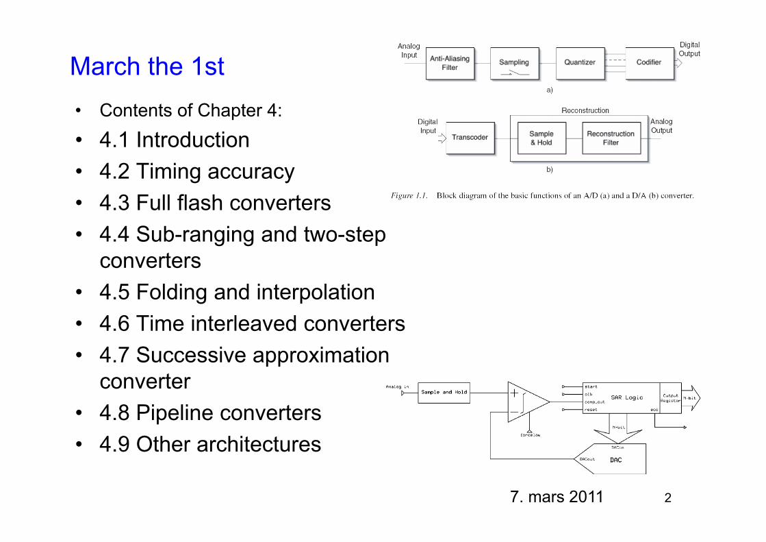
March the 1st• Contents of Chapter 4:
• 4.1 Introduction• 4.2 Timing accuracy• 4.3 Full flash converters4.3 Full flash converters• 4.4 Sub-ranging and two-step
converters• 4.5 Folding and interpolation• 4.6 Time interleaved converters• 4.7 Successive approximation
converter• 4.8 Pipeline converters• 4.9 Other architectures
27. mars 2011

March the 8th –Switched Capacitor Circuits
• Intro to SC-circuits• 12.3 Switched Capacitor Amplifiers• 12.3.1 Unity-Gain Sampler / Buffer12.3.1 Unity Gain Sampler / Buffer• 12.3.2 Noninverting amplifier• 12.4 Switched-Capacitor Integrator12.4 Switched Capacitor Integrator• Examples, incl. Oversampling
converters.• Report Writing
37. mars 2011

Folding and interpolation g p

Switched Capacitor Circuitsp• Sensing / sampling the input only at
periodic instants of time processingperiodic instants of time, processingthe each sample and producing a valid output at the end of each
i d ”di t ti ” ” l dperiod; ”discrete-time” or ”sampled-data” systems.
• Simple building blocks like samplers, p g pamplifiers and integrators providethe foundation for more advancedcircuits and topics.circuits and topics.
• Filters, comparators, (oversampling) ADCs and DACs.
• Well suited for CMOS implementation, due to goodswitches (low Ron, no offset) and onhigh input impedance amplifiers.
5test

Properties of SC circuitsP l d t t f d li it• Popular due to accurate frequency response, good linearityand dynamic rangeEasily analyzed with z transform• Easily analyzed with z-transform
• Typically require aliasing and smoothing filtersA i bt i d i filt ffi i t d t i d• Accuracy is obtained since filter coefficients are determinedfrom capacitance ratios, and relative matching is good in CMOSCMOS
• The overall frequency response remains a function of theclock, and the frequency may be set very precisely through, q y y y p y gthe use of a crystal oscillator
• SC-techniques may be used to realize other signal y gprocessing blocks like for example gain stages, voltage-controlled oscillators and modulators

Basic building blocks in SC circuits; Opamps, capacitors, switches, clockgenerators
• DC gain typically in the order of 40 to 80 dB (100 – 10000 x)• Unity gain frequency should be > 5 x clock speed (rule ofUnity gain frequency should be > 5 x clock speed (rule of
thumb)• Phase margin > 70 degrees (according to ”Johns & Martin”)Phase margin 70 degrees (according to Johns & Martin )• Unity-gain and phase margin highly dependent on the load
capacitance, in SC-circuits. In single stage opamps ap , g g p pdoubling of the load capacitance halves the unity gainfrequency and improve the phase margin
• The finite slew rate may limit the upper clock speed.• Nonzero DC offset can result in a high output dc offset,
depending on the topology chosen, especially if correlateddouble sampling is not used

Basic building blocks in SC circuits; Opamps, capacitors, switches, clock generatorsp , , g
C1
C
Cp1
poly1
poly2
thin oxide
hi k id
metalmetal
C1bottom plateCp2poly2 thick oxide
Cp2Cp1
p
(substrate - ac ground)
• Typically constructed between two polysilicon layerscross-section view equivalent circuit
• Parasitics; Cp1, Cp2.• Parasitic Cp2 may be as large as 20 % of the desired, C11•• Cp1 Cp1 typicallytypically 11-- 5 % 5 % ofof C1. C1. ThereforeTherefore, , thethe equivalentequivalent modelmodel
containcontain 3 3 capacitorscapacitors

Basic building blocks in SC circuits;Opamps, capacitors, switches, clock generatorsOpamps, capacitors, switches, clock generators
v1
v1
v2
v2
Symbol n-channel
v1 v
2
h l
transmissiongate
• Desired: very high off-resistance (to avoid leakage), relatively low
v1 v
2
2
p-channel
y g ( g ) yon-resistance (for fast settling), no offset
• Phi, the clock signal, switches between the power supply levels• Convention: Phi is high means that the switch is on (shorted)• Transmission gate switches may increase the signal range
S id l ff t li it h id f th• Some nonideal effects: nonlinear capacitance on each side of the switch, charge injection, capacitive coupling to each side

SC Resistor Equivalent (1/2)
21
V1 V2V1 V2
Req
C1
Req
TC
1------=
Q C1
V1
V2– every clock period=
Qx CxVx=
Q1 C1 V1 V2– =C1 is first charged to V1 and then charged to V2 during one clock cycle
C1 V1 V2–
The average current is then given by the change in charge during one cycle
Iavg1 1 2
T-------------------------------=
Where T is the clock period (1/fs)

SC Resistor Equivalent (2/2)q21
V1 V2V1 V2
Req
C1
Req
TC
1------=
Q C1
V1
V2– every clock period=
The current through an equivalent resistor is given by:
Combining the pre io s eq ation ith Ia g
IV1 V2–
Combining the previous equation with Iavg:
Ieq Req-------------------=
The resistor equivalence is valid when fs is much larger than the signal
ReqTC1------ 1
C1fs----------= =
The resistor equivalence is valid when fs is much larger than the signal frequency. In the case of higher signal frequencies, z-domain analysis is required :

Example of resistor implementation
• What is the resistance of a 5 pF capacitancesampled at a clock frequency of 100 kHz?sampled at a clock frequency of 100 kHz?
• Note the large resistance that can be implemented.C OS fImplemented in CMOS it would take a large area for
a plain resistor of the same resistance
1Req1
5 10 12– 100 103
-------------------------------------------------------- 2M= =5 10 100 10

An inverting integrator
vc2
nT( )
21
C2 1
vc
t( ) 2
C
1
vci
t( )
cx
vco
t( )
v t( ) C1
vo
n( ) vco
nT( )=vi
n( ) vci
nT( )=
vc1
t( )

First-Order Filters
Vin s( ) Vout s( )
• Select a known Active-RC circuit• Replace resistors by SC-equivalentsp y q• Analyze using discrete-time methods

Unity-Gain Sampler/Buffer• A unity gain amplifier can be
realized with no resistors andrealized with no resistors and capacitors in the feedback, butstill requires a sampling circuit(Fig 12 29 b))(Fig. 12.29 b))
• The input-dependent chargeinjected by S1 onto CH limits the accuracy.
• We’ll see a SC-implementationthat does not have significantgproblems with charge injection, if proper clocking is used (Fig 12 30)(Fig. 12.30).
• Three switches control theoperation.

Unity-Gain Sampler/ buffer in sampling and amplification mode
S l S d S S ff F hi h i V V 0 d• Sample: S1 and S2 are on, S3 off. For a high gain opamp, VB=Vout≈0 and the voltage accross C1 equal to Vin.
• Amplify: S3 on, S1 and S2 are off.A to ground. Since VA changes from Vinp y 3 , 1 2 g A g into 0, Vout changes to Vin0C1/C2.

Continous time implementation vs the SC implementation
• The SC implementation samples the input, setting the output to zero and provides amplification of the input in the next period, while ignoring the input voltage. The circuit configuration changes from one phase to another, raisingstability concerns.
• When Vout have settled, the current through C2 approaches zero, while R2continously loads the amplifier.

Unity-Gain Sampler/Amplifier ; turning S2 off slightly before S1,to avoid problems with charge injection
S V 0 d S i j t ∆ 1 t
• Fig. 12.31 shows ”slow motion”; S2injects ∆q2 onto CH producing an error
• Suppose Vin=0 and S1 injects ∆q1 ontoP .Cx is the total capacitance from X to ground. The total charge at X cannotchange after S turned off (no dc pathj q H, p g
∆q2 / CH , which is quite independent (The body effect makes VTH a functionof Vin) of the input level since node X is
change after S2 turned off (no dc pathin or out). The same holds true after CHis placed around the opamp. The output voltage is not influenced by
• After the feedback circuit has settled, the
at virtual ground. Only an offset (ratherthan gain error or nonlinearity is produced)
output voltage is not influenced by charge injection due to S1.
charge on CH equals V0CH, unaffectedby S3 (S3 introducing no error).
• ∆q = WLCOX Veff = WLCOX (VGS – VTH) = WLCOX (VCK – VX - VTH)

Unity-Gain Sampler/Amplifier and generation of proper clock edges –ensuring that S1 turns off after S2 does
• Skewed clocks (left) oftenused for example inused, for example in Sigma-Delta modulators for oversamplingfor oversampling converters.
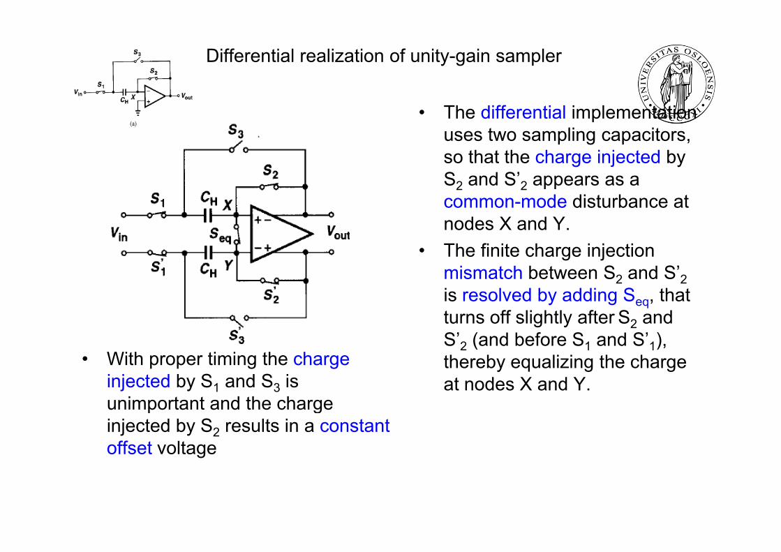
Differential realization of unity-gain sampler
• The differential implementationuses two sampling capacitors,
th t th h i j t d bso that the charge injected by S2 and S’2 appears as a common-mode disturbance at nodes X and Y.
• The finite charge injectionmismatch between S2 and S’2mismatch between S2 and S 2 is resolved by adding Seq, thatturns off slightly after S2 and S’ (and before S and S’ )
• With proper timing the chargeinjected by S1 and S3 is unimportant and the charge
S 2 (and before S1 and S 1), thereby equalizing the chargeat nodes X and Y.
unimportant and the chargeinjected by S2 results in a constantoffset voltage

unity-gain sampler precision considerations
• The input capacitance• The input capacitanceshould be minimized evenif speed is not critical.if speed is not critical. (Larger input transistors mean higher Cin.)
• A finite input capacitance, Cin, is assumed.I th lifi ti d th i it• In the amplification mode the circuitfrom Fig. 12.30 operates as a unity-gain buffer. How close to unity?

Noninverting amplifier ; final output having same polarity as Vin0 and thepossibility of gain > 1.
• Since Vp goes from Vin0 to p0, the output voltagechanges from 0 to approximately Vin0(C1/C2).
• Input dependent charge injectionis again avoided by proper
S ff f S
pp y in0( 1 2)
timing, turning S2 off before S1. Vout is free for errors due to S1and S3 , and offset due to S2 can,be suppressed by differentialoperation (Fig. 12.46).
• Sample: S1 and S2 on, S3 off. Virtual ground at X. The voltageaccross C tracks V At the end ofaccross C1 tracks Vin. At the end ofthe sampling mode, S2 turns off, injecting ∆q2 on X.Subsequently S1t ff d iturns off, and in
• Amplification mode, S3 turns on.

Noninverting amplifier – timing and behaviour
• After S3 turns on, Vp drops to zero. Thus the overall change in Vp is equalt 0 V V d i llto 0-Vin0=-Vin0, producing an overall change in the output equal to –Vin0(-C1/C2)=Vin0C1/C2
• Vp goes through an intermediateperturbation but the output of interest is measured after P is connected to
d th t h i j t d b Sground, so that charge injected by S1does not affect the final output.
• From S2 turns off to S1 turns off, Vind h h d
• S2 turns off before S1, making thei i i i i h i j i
may undergo changes that does not introduce any error; sampling instant is defined by the turn-off of S2.
circuit insensitive to charge injection(total charge at X constant) of S1 or charge ”absorption” of S3.
• In summary: Proper timing ensures thatnode X is perturbed by only the chargeinjection of S2, making the final Vout freef d t S d S Off t• ∆q1 gives rise to ∆Vp= ∆q1/C1, and
the output voltage by -∆q1/C2.
from errors due to S1 and S3. Offset due to S2 may be suppressed by differential operation

Noninverting amplifier – timing and behaviour
• In summary: Proper timing ensures thatnode X is perturbed by only the chargei j ti f S ki th fi l V finjection of S2, making the final Vout freefrom errors due to S1 and S3. Offset due to S2 may be suppressed by differential operationdifferential operation.
• Differential implementation shown in Figure 12.46.

Switched Capacitor Integrator
• Used in filters and oversampling ADCs.p g• For sampled data systems we use a
discrete time counterpart to the continoustime integrator.g
• Continous time resistor:I = (VA-VB)/R• SC: Iav = Cs(VA-VB)fCK
-1 = Cs(VA-VB)fCK; the
average current flowing from A to B beingaverage current flowing from A to B beingthe charge moved in one clock period.
• A resistance is simulated by the SC-circuit.Fi 12 54 h th di t ti• Figure 12.54 shows the discrete time integrator.
• In every clock cycle C1 absorbs a chargel t C V h S i d d itequal to CinVin when S1 is on and deposits
the charge on C2 when S2 is on. Approximating the staircase with a ramp,
t th t th i it b hwe note that the circuit behaves as an integrator.

Switched Capacitor Integrator -drawbacks
• Input dependent charge injection of S1 introduces nonlinearity in the chargestored on C1 and hence the output voltage.Th li it t d P lti f S/D j ti f S d• The nonlinear capacitance at node P resulting from S/D junctions of S1 and S2 leads to nonlinear charge to voltage conversion when C1 is switched to X, giving an nonlinear component at the output.
• An integrator topology that resolves both issues may be found (in Fig. 12.56 a)) in ”Razavi”.

Transfer function for simple discrete time integrator
•

Improved Switched Capacitor Integrator without charge injection problems
• Sampling mode: S1 and S3 on, C1 tracks Vin.• In the transition to the integration mode S3g 3
turns off first, injecting a constant charge ontoC1. S1 turns off next, and subsequently S2and S4 turns on (Fig. 12.56 c)). The charge
C f Cstored on C1 is transferred to C2 via the virtualground node. Since S3 turns off first, it introduces only a constant offset, which canbe suppressed by differential operationbe suppressed by differential operation.
• Moreover, since the left plate of C1 is ”driven” (section 12.3.2), the charge injection or absorption of S1 and S2 contributes no error
• ∆q = WLCOX V ff =
absorption of S1 and S2 contributes no error. • Also, since node X is a virtual ground, the
charge injected or absorbed by S4 is constantand independent of Vin.∆q = WLCOX Veff =
WLCOX (VGS – VTH) and independent of Vin.
• Nonlinear junction capacitances of S3 and S4 have voltages going from near zero in saplingmode to virtual ground in integration mode g gnegligible nonlinear contribution to the output voltage.

Unity-Gain Sampler/Amplifier and generation of proper clock edges –ensuring that S1 turns off after S2 does
• Similar integrators widelyused in oversampling ADCsexploiting SC ∆Ʃexploiting SC ∆Ʃ modulators/Ʃ ∆ modulators

Improved Switched Capacitor Integrator
• Sampling mode: S1 and S3 on, C1tracks Vin.
• In the transition to the integration• In the transition to the integrationmode S3 turns off first, injecting a constant charge onto C1. S1 turnsoff next and subsequently S2 andoff next, and subsequently S2 and S4 turns on (Fig. 12.56 c)). The charge stored on C1 is transferredto C2 via the virtual ground node. o C2 a e ua g ou d odeSince S3 turns off first, it introducesonly a constant offset, which can be suppressed by differentialpp yoperation.

Litterature• Razavi, chapter 12.3, 12.4: Introduction to Switched Capacitor Circuits
31

Next week, 15/03:
• Next week: Oversampling converters, from chapter 14 in Johns & MartinJohns & Martin.
• Messages are given on the INF4420 homepage.
• Questions: [email protected] , 22852703 / 90013264