Embed Size (px)
Citation preview
Research article
Received: 22 June 2014 Revised: 27 August 2014 Accepted: 28 August 2014 Published online in Wiley Online Library: 30 September 2014
(wileyonlinelibrary.com) DOI 10.1002/sia.5677
Surface structure and photoluminescenceproperties of AZO thin films onpolymer substratesNihan Akin,a,b* Yunus Ozen,a,b H. Ibrahim Efkere,a,b Mehmet Cakmaka,b
and Suleyman Ozcelika,b
Al-doped zinc oxide (AZO) thin films were deposited on indium tin oxide (ITO) coated polyethylene terephthalate (PET) substratesby radio frequency (RF) magnetron sputtering method at room temperature. The effects of film thickness on the surface structureand the photoluminescence properties of the films were investigated by atomic forcemicroscopy (AFM), secondary ionmass spec-troscopy (SIMS) and room temperature photoluminescence (PL). AFM analysis showed that the surface of all films was extremelyflat and uniform at nanoscale. Root mean square (RMS) value of the surface roughness which scanned the surface area of 3μmby3μmand grain size increased with increasing the film thickness. Thus, the surfacemorphology of the films became rough becauseof the coarse grains. The depth profile of AZO layers was analyzed by SIMS. It was found that the thickness of the AZO layer isalmost same with the desired film thickness. The PL intensity of the dominant peak decreased and shifted slightly towards theshorter wavelengths with increasing the film thickness. According to the relationships between luminescence intensity andcrystalline characteristics, it was observed that the intensity of the peak decreased by the increased surface area of the grains.Copyright © 2014 John Wiley & Sons, Ltd.
Keywords: radio frequencymagnetron sputtering; AZO thin films; atomic forcemicroscopy; secondary ionmass spectroscopy; photoluminescence;polymer substrates
* Correspondence to: Nihan Akin, Department of Physics, Gazi University, 06500Ankara, Turkey.E-mail: [email protected]
a Photonics Application and Research Center, Gazi University, 06500, Ankara,Turkey
b Department of Physics, Gazi University, 06500, Ankara, Turkey
93
Introduction
Transparent conducting Al-doped zinc oxide (AZO) thin films havebeen commonly investigated because of their potential applica-tions in optoelectronics such as gas sensors, UV detectors, flat paneldisplays (FPDs), light-emitting diodes (LEDs), organic light-emittingdiodes (OLEDs) and organic photovoltaic (OPV) devices.[1–3] Forthese applications, AZO thin films have been deposited on severalkinds of polymer substrates.[4–7] The films deposited on polymersubstrates have many special merits compared with those depos-ited on glass, silicon, sapphire and quartz substrates due to theirlight weight and small volume. It can make the obtained devicesportable, foldable and easy to carry. Thus, they can be used inflexible electrical and optical devices, unbreakable heat-reflectingmirrors, plastic liquid crystal display devices and transparentelectromagnetic shielding materials.[8]
Besides the AZO layer being used as transparent conductingelectrode, it can be deposited as a buffer layer on indium tin oxide(ITO) coated flexible polyethylene terephthalate (PET) substrates foropto-electronic devices. ZnO thin films on the ITO coated substratehave a role to improve the electron transport between electrodeand active layer as well as reduce the oxidation of the electrodein the organic optical devices.[9] Surface morphology is transferredto the functional organic layers deposited subsequently, giving anuneven interface which is not desirable for device efficiencyand stability.[10] AZO/ITO/PET structures have improved deviceefficiency compared to single-layer TCO electrode, owing to betterelectrical conductivity and mechanical stability. In addition, theoptical transmission which is the most important parameter for
Surf. Interface Anal. 2015, 47, 93–98
optical devices is increased by coating of AZO thin films on theITO.[11–14] However, surface morphological and emission propertiesof deposited high quality AZO thin films on ITO coated flexible PETsubstrates have not been sufficiently investigated in the literature.
Alternatively, development of bilayer AZO/ITO transparentconducting oxide (TCO) electrodes is very important to the ITO-basedorganic solar cells. The AZO layer protects degradation in ITO-basedorganic solar cells due to its tailored UV absorption, serving as aUV filter to prolong the lifetime of the devices.[15] This is an advan-tage of AZO/ITO/PET structures for eventual device applications.
TCO thin films should have both good optical transparency andelectrical conductivity to develop better performance optoelec-tronic device applications. In our previous work, the transparencyand conductivity properties of AZO/ITO/PET structure depend onthe AZO thin film thickness which is presented in this work havebeen detailed investigated.[11] Our results have shown that thecoating has not strongly affected on the optical transmittanceand sheet resistivity. While bare ITO/PET substrate has been around80% transmittance, the prepared samples have been slightly below
Copyright © 2014 John Wiley & Sons, Ltd.

N. Akin et al.
94
80% transmittance. In addition, the sheet resistivity of ITO/PET sub-strate is 13.11Ohm/sqr, and the coated samples with thickness of52, 80, 102 and 136nm are 11.32, 10.06, 12.84 and 14.19Ohm/sqr,respectively.Various deposition techniques have been performed to prepare
AZO thin films such asmagnetron sputtering[1–8] sol–gel,[16] chemicalvapor deposition (CVD),[17] metal–organic chemical vapor deposition(MOCVD),[18] spray pyrolysis,[19] pulsed laser deposition (PLD),[20] elec-tron beam evaporation[21] etc. Among these methods, magnetronsputtering is the most widely used ones due to uniformity, easyfabrication and parameter controllability. High quality films can beobtained by optimization of the deposition parameters such assputtering pressure, film thickness, power, gas flux and target-substrate distance, etc.The performance of any semiconductor devices significantly
depends on the surface morphology, impurity in surface andinterface, and abruptness of the interface.[22] Secondary ion massspectroscopy (SIMS) gives excellent information about of alloycomposition, atomic homogeneity and interface characteristics ofgrown layers with its depth profile measurements capability inppm range.[22–24]
Figure 1. 3D and 2D AFM images of AZO thin films with various thickness. Th
wileyonlinelibrary.com/journal/sia Copyright © 2014 Jo
In this work, the effects of film thickness on morphological andoptical properties of RF-sputtered AZO thin films on ITO coated PET(ITO/PET) substrates by using atomic force microscopy (AFM) andphotoluminescence (PL) techniques were presented. Surface mor-phology, film growth mode and surface roughness could bechanged with the change of the film thickness, and these factorswould affect the optical properties. In literature, it was seen thatthe luminescence intensity depends on the surface area of the grains.The materials with smaller crystallites showed higher luminescenceintensity compared to the larger crystallites. Lai et al. reported thatthe increase of surface roughness would enhance the optical scatter-ing and optical loss.[25] Prathap et al. studied the influence of filmthickness on the optical band gap as well as the luminescence inten-sity and showed that the reduction in the intensity of the lumines-cence clearly indicated the influence of the surface area of thegrains on the luminescence.[26] Also, we found that the similar opticalresults from the photoluminescence (PL) spectra in this presentedwork. The PL intensity of the films decreased and shifted slightlytowards the shorter wavelengths with increasing the film thickness.In addition, atomic distributions and interface abruptness indeposited AZO thin films were analyzed by SIMS measurements.
e scan area is 3× 3 μm2 in the all images.
hn Wiley & Sons, Ltd. Surf. Interface Anal. 2015, 47, 93–98

Table 1. Some structural and morphological parameters of AZO thin films
aThickness(nm)
b Grain size(nm)
c Grain size(nm)
RMS(nm)
dAverage heightZav (nm)
Maximum heightZmax (nm)
Relative heightZR(Zav/Zmax)
52 16.5 23.4 2.97 12.60 24.66 0.51
80 41.2 35.1 3.30 12.80 23.53 0.55
102 42.8 37.0 3.40 14.96 23.29 0.64
136 43.5 58.5 3.44 11.84 23.24 0.51
aDetermined from SIMS depth profile.bCalculated from XRD measurements using Scherrer’s formula in our previous study.[11]
cEvaluated from Fig. 1, by measuring the size of hillock.dCalculated from surface profiles in Fig. 3.
High quality AZO thin films on ITO/PET substrates
Experimental details
AZO thin films were deposited on inexpensive ITO/PET substratesby using radio frequency (RF) magnetron sputtering system(BESTEC GmbH, Berlin, Germany) in an argon (Ar) gas atmosphere.A ceramic ZnO:Al2O3 (2wt.%) target (purity: 99,99%) was used forthe deposition of the films. The substrates were ultrasonically
Figure 2. Root mean square (RMS) values of the surface roughness of AZOthin films.
Figure 3. Surface profiles of AZO thin films. The scan area is 3× 3 μm2 in the a
Surf. Interface Anal. 2015, 47, 93–98 Copyright © 2014 John W
cleaned in acetone and then alcohol for 5min, respectively,before they were loaded into the deposition chamber. Thesputtering system was pumped down to pressure 3.9× 10�8mbarfor more than 12h by using a turbomolecular pump and controlledby using an ion gauge controller. In order to investigate the effectof the film thickness on the properties of the films, the film thick-ness was varied from 50nm to 125nm. RF power was set at100W for the all samples. Sputtering pressure (PS) was kept at3.0 × 10�3mbar, and the temperature of the substrate was main-tained at room temperature (RT). The distance between targetand substrate was about 35mm.
The surface morphology of the films was characterized witha high performance atomic force microscope (NanoMagneticsInstruments Ltd., Oxford, UK) by using dynamic mode scan-ning. A single crystal silicon tip was attached to the end ofa cantilever oscillating at or near its resonant frequency(146–236 kHz). The scan area was set at 3 × 3 μm2, and thescan speed was 1μm/s. A topographic image consisted of 256lines. All measurements were made at room temperature (RT).The root mean square (RMS) value of the surface roughnessof the films was calculated from AFM images which was de-fined as: RMS (nm) = [ Σ (zi� zave)
2 / N ]1/2 where zi is the cur-rent value of z, zave is the mean value of z in the scan areaand N is the number of points. In order to characterize forinterfaces and atomic distribution or local composition, the
ll cases.
iley & Sons, Ltd. wileyonlinelibrary.com/journal/sia
95

N. Akin et al.
96
depth profile of AZO layers was performed by SIMS (HidenAnalytical Ltd., Warrington, UK). Bombardment was donewith 5-keV O2 (oxygen) ions. The primary ion current was200 nA for the O2 oxygen beam. The secondary ions werecollected from the central area of 100 μm2. During the SIMSexperiments, the base pressure of the chamber was kept at10�10 mbar. The optical properties of the films were performedby room temperature PL measurements (HORIBA JobinYvon Ltd.,Stanmore, UK) by using a 50-mW HeCd laser (λ =325nm) whichis an excitation light source.
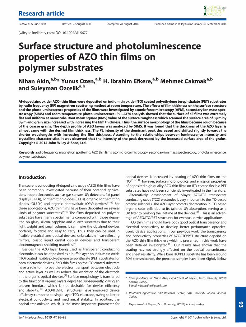
Figure 4. SIMS depth profile of AZO thin films with various thicknesses.
Results and discussions
Morphological studies
The surface morphology is a very important factor for a transparentconducting thin films, because a non-uniform surface can causebreakdown or shortening with upper layers and can cause seriousproblems on the performance of electrical and optical devices.Because of these reasons, various methods have been developedto analyze the surface. AFM is used to characterize the surfaceand also to estimate grain size and surface roughness. Figure 1shows that three-dimensional (3D) and two-dimensional (2D) AFMimages with 3×3μm2 scan area of four RF-sputtered AZO thin filmson ITO/PET substrates. It can be seen that with increasing the filmthickness, the crystallinity of the films is improved, and the grainsizes become larger. The grain size is evaluated from AFM imagewhich increase from 23.4 to 58.5 nm with increasing the filmthickness from 52 to 136nm. This parameter nearly matches withcalculated from the XRD measurements in our previous work,[11]
as seen in Table 1. The rootmean square (RMS) values of the surfaceroughness of the films are shown in Fig. 2 and listed in Table 1. TheRMS roughness increases from 2.97 to 3.44 nm when the filmthicknesses increase from 52 to 136nm. The increase of roughnessis associated with the increase of grain size. Similar results were alsoreported in sputtered transparent conducting oxide (TCO) thin filmswith different thickness.[27–29] Moreover, the RMS of the bareITO/PET substrate is 2.01nm. This value shows that the coating isnot a big influence on the RMS of the substrate surface.In order to obtain the detailed surface structure analysis, we
defined relative height rh = Rav / Ry, in which Rav and Ry are theaverage height and maximum height in every AFM image, respec-tively. Average heights (Rav) of the surface of the films are calculatedfrom 3×3μm2 AFM scan areas, as seen in Fig. 3, B. Z. Dong et al.reported that when relative height (rh) is bigger than 0.5, thesurface tends to be hillock morphology; otherwise, the crateredmorphology is often observed.[30] In light of this knowledge, itcan be said that there is not cratered morphology in our all samplesbecause of the rh bigger than 0.5 in the all. Besides, rh values areclose to each other, and, consequently, brightness is almost thesame in the all AFM images under the same color setting.In this presented work, reference sample was not used in the
SIMS analyses; however, the thickness of AZO layers can be stilldetermined from the SIMS depth profiles as seen in Fig. 4. Thedepth calibration of the sputtered crater was performed by Dectac150 profilometer. AZO thin films with thickness of 50nm, 75 nm,100nm and 125nm are found to be as 52nm, 80 nm, 102nm and136nm, respectively. It can be seen that the thickness of the AZOlayer is almost same with the measured thickness by thicknesssensor during the deposition. The depth profiles can be used toexamine the distribution of elements, and, therefore to understandthe sharpness of the interface of AZO/ITO, main elements (Al, Zn, In
wileyonlinelibrary.com/journal/sia Copyright © 2014 Jo
and Sn) in the layers were detected by mass spectrometer. Figure 4shows that the depth profile of Al, Zn, In and Sn has a sharp inter-face at 52 nm, 80nm, 102nm and 136nm, respectively. Zn and Al
hn Wiley & Sons, Ltd. Surf. Interface Anal. 2015, 47, 93–98

High quality AZO thin films on ITO/PET substrates
have been seen to diffuse deeper into the ITO layer, and their diffu-sion depth was increased with thickness of the AZO thin film. Thismay be explained with the influence of the energetic ions due tothe sputtering process. In addition, there is no significant variationof the distribution of the Zn in the deposited AZO layers.
Photoluminescence studies
Figure 5 represents the RT PL spectra of the AZO thin films onITO/PET substrates. It can be seen that all samples show a typicalluminescence behavior with the emission of a dominant intensitypeak centering around 392nm. The intensity of the peak decreasedas the film thickness increased being strongly dependent on thegrain surface area. In order to well define band gap or excitonicemission, it is necessary to control the surface states. In general,the density of the surface states decreases with the grain sizeincrease. Also, luminescence intensity decreases with decrease ofthe density of the surface states due to small surface to volumeratio for the larger crystallites. Thus, the films with smaller crystal-lites could show higher luminescence intensity compared to thelarger crystallites. From Fig. 6, it can be seen that both the PL FWHMand PL peak position of the emission spectra are dependent on filmthickness. The emission peak position shifts slightly towards theshorter wavelengths with increasing the film thickness. In addition,the PL intensity of the dominant peak decreased and shiftedslightly towards the shorter wavelengths with increasing the filmthickness. According to the relationships between luminescenceintensity and surfacemorphology obtained by AFMmeasurements,
Figure 6. PL FWHM and PL peak position of AZO thin films.
Figure 5. RT PL spectra of AZO thin films.
Surf. Interface Anal. 2015, 47, 93–98 Copyright © 2014 John W
it was observed that the intensity of the peak decreased by theincreased surface area of the grains.
In addition, investigating the structural parameters such ascrystallinity, lattice constant and grain size etc. is importantto understand the PL results of the films. As well known, theoptical properties of the AZO thin films are affected by themicrostructure of the films.[31] In our previous work, we haveinvestigated the structural properties of the AZO thin filmsdepending on the film thickness, using X-ray diffractometer.[11]
With increasing the film thickness, the crystalline quality hasbeen improved, and the grain sizes became larger. An increasein grain size can be effective on the concentration of localizedexcitons, and this case may be lead to decrease of the oxygenvacancy in the films. Consequently, the PL intensity of the filmsmay decrease with increasing the grain size, as in our work.
97
Conclusions
AZO thin films were successfully deposited on ITO/PETsubstrates by RF magnetron sputtering at RT. The morphologicaland photoluminescence properties of the films were investi-gated depending on the film thickness. AFM measurementsshowed that with increasing the film thickness, the crystallinityof the films was improved, and the grain sizes became larger.The grain size was evaluated from AFM image which increasesfrom 23.4 to 58.5 nm with increasing the film thickness from 52to 136 nm. SIMS depth profiles of AZO/ITO interface of thesamples had good sharpness. Diffusion of Zn and Al into theITO layer was observed with a small penetration depth. However,there was no significant effect on the PL emission of the AZOthin films with this atomic diffusion. In addition, it was observedthat the films with smaller crystallites could show higher lumi-nescence intensity compared to the larger crystallites.
Acknowledgements
This work was supported by the Ministry of Development of TRunder Project No: 2011K120290.
References[1] S. M. Chou, L. G. Teoh, W. H. Lai, Y. H. Su, M. H. Hon, Sensors 2006, 6, 1420.[2] X. Jiang, F. L. Wong, M. K. Fung, S. T. Lee, Appl. Phys. Lett. 2003, 83, 1875.[3] H. Zhu, J. Hupkes, E. Bunte, A. Gerber, S. M. Huang, Thin Solid Films 2010,
518, 4997.[4] J. Y. Kao, C. Y. Hsu, G. C. Chen, D. C. Wen, J. Mater. Sci. - Mater. Electron.
2012, 23, 1352.[5] X. J. Wang, Q. S. Lei, W. Xua, W. L. Zhou, J. Yu,Mater. Lett. 2009, 63, 1371.[6] Y. C. Lin, M. Z. Chen, C. C. Kuo, W. T. Yen, Colloids Surf., A 2009, 337, 52.[7] J. M. Kim, P. Thiyagarajan, S. W. Rhee, Thin Solid Films 2010, 518, 5860.[8] S. H. Jeong, J. H. Boo, Thin Solid Films 2004, 447-448, 105.[9] H. J. Park, K. H. Lee, B. Kumar, K. S. Shin, S. W. Jeong, S. W. Kim,
J. Nanoelectron. Optoelectron. 2010, 5, 1.[10] Y. H. Tak, K. B. Kim, H. G. Park, K. H. Lee, J. R. Lee, Thin Solid Films 2002,
411, 12–16.[11] N. Akin, S. S. Cetin, M. Cakmak, T. Memmedli, S. Ozcelik, J. Mater. Sci. -
Mater. Electron. 2013, 24, 5091.[12] B. Y. Oh,W. K. Lee, Y. H. Kim, D. S. Seo, J. Appl. Phys. 2009, 105, 054506-1.[13] J. B. Franklin, B. Zou, P. Petrov, D.W.McComb,M. P. Ryan, M. A.McLachlan,
J. Mater. Chem. 2011, 21, 8178.[14] M. S. White, D. C. Olson, S. E. Shaheen, N. Kopidakis, D. S. Ginley, Appl.
Phys. Lett. 2006, 89, 143517.[15] H. Liu, Z. Wu, J. Hu, Q. Song, B. Wu, H. L. Tam, Q. Yang, W. H. Choi, F. Zhu,
Appl. Phys. Lett. 2013, 103, 043309.[16] K. E. Lee, M. Wang, E. J. Kim, S. H. Hahn, Curr. Appl. Phys. 2009, 9, 683.
iley & Sons, Ltd. wileyonlinelibrary.com/journal/sia

N. Akin et al.
98
[17] D. Kim, I. Yun, H. Kim, Curr. Appl. Phys. 2010, 10, 459.[18] M. E. Fragala, G. Malandrino, M. M. Giangregorio, M. Losurdo, G. Bruno,
S. Lettieri, L. S. Amato, P.Maddalena, Chem. Vap. Deposition 2009, 15, 327.[19] B. J. Babu, A. Maldonado, S. Velumani, R. Asomoza, Mater. Sci. Eng. B
2010, 174, 31.[20] S. J. Kang, Y. H. Joung, J. Mater. Sci. - Mater. Electron. 2013, 24, 1863.[21] D. R. Sahu, S. Y. Lin, J. L. Huang, Microelectron. J. 2007, 38, 245.[22] B. R. Chakraborty, Appl. Surf. Sci. 2004, 221, 143.[23] K. Kadoiwa, K. Ono, Y. Ohkura, J. Cryst. Growth 2006, 297, 44.[24] A. Y. Peng, Y. Hua, M. Ting, W. Y. Ding, T. J. Hua, X. C. Dong, Chin. Phys.
Lett. 2010, 27017302, 1.
wileyonlinelibrary.com/journal/sia Copyright © 2014 Jo
[25] F. Lai, L. Lin, Z. Huang, R. Gai, Y. Qu, Appl. Surf. Sci. 2006, 253, 1801.[26] P. Prathap, N. Revathi, Y. P. V. Subbaiah, K. T. R. Reddy, J. Phys. Condens.
Matter 2008, 20, 035205-1.[27] X. Hao, J. Ma, D. Zhang, T. Yang, H. Ma, Y. Yang, C. Cheng, J. Huang, Appl.
Surf. Sci. 2001, 183, 137.[28] K. H. Kim, R. A. Wibowo, B. Munir, Mater. Lett. 2006, 60, 1931.[29] S. Venkatachalam, H. Nanjo, F. M. B. Hassan, K. Kawasaki, M. Kanakubo,
T. Aizawa, T. Aida, T. Ebina, Thin Solid Films 2010, 518, 6891.[30] B. Z. Dong, G. J. Fang, J. Appl. Phys. 2007, 101, 033713-1.[31] T. Moon, W. Yoon, K. S. Ji, S. W. Ahn, S. Lee, M. Joo, H. Y. Shin, K. Park,
H. M. Lee, Appl. Phys. Express 2010, 3, 095801.
hn Wiley & Sons, Ltd. Surf. Interface Anal. 2015, 47, 93–98