Embed Size (px)
Citation preview

PHOTOEMISSION, PHOTOLUMINESCENCE AND
PHOTOCONDUCTIVITY O F SOLIDS IN THE
VACUUM ULTRAVIOLET REGION
BY
William Pong
F ina l Report
May 1970
The r e s e a r c h was supported b y
NATIONAL AERONAUTICS AND SPACE ADMINISTRATION
Gran t NsG-328 (NGR 12-001-002)
Department of Phys ics and Astronomy Univers i ty of Hawaii, Honolulu, Hawaii 96822

PHOTOEMISSION, PHOTOLUMINESCENCE AND
PHOTOCONDUCTIVITY O F SOLIDS IN THE
VACUUM ULTRAVIOLET REGION
BY
Will iam Pong
F ina l Repo r t
May 1970
The r e s e a r c h was supported by
NATIONAL AERONAUTICS AND SPACE ADMINISTRATION
Gran t NsG-328 (NGR 12-001-002)
Depar tment of P h y s i c s and As t ronomy Univers i ty of Hawaii, Honolulu, Hawaii 96822

This report contains an account of several years of research
on the interact ion of photons with gases and sol ids i n the spec t ra l 0
region of 2000 t o 500 A . While the principal aim was t o investigate
the photoelectric properties of sol ids , the study of gases was in-
cluded t o provide a convenient secondary standard fo r absolute yield 0
measurements below 1000 A. By comparing the ion current with the
response of a calibrated thermocouple, the photo-ionization yield of 0
xenon was found t o be unity i n the region 800-1000 A.
The spectral quantum yields of a number of photoemissive films,
e .g . , a lka l i halides, CuI, Se, Te, Au, A l , ,.., were measured.
Some alkali-halide films have yields of approximately unity at photon
energies s l ight ly above twice the photoelectric threshold of the mate-
r i a l , Photoemission frm evaporated MgF2 i n the region of exciton
absorption was measured; the resu l t s appear t o be compatible with the
viewpoint tha t exciton s ta tes may be present i n the conduction band
of MgF2. I n addition t o the spectral-yield measurements, the escape
length fo r photoelectrons i n evaporated films such as CuBr, KBr, gold,
and aluminum were estimated from the yield vs film-thickness data ,
Exciton-induced photoemission from evaporated KC1 films was ob-
served. The ef fec t of biasing radiation (vis ible l igh t ) on the inter-
act ion between excitons and F-centers was investigated. An application
of t h i s effect i s suggested.
Preliminary studies of photol~~minescence of sodium sa l icy la te and
photoconductivity of insulating crystals i n the vacuum ul t rav io le t are
discussed.

T A B L E O F C O N T E N T S
CHAPTER PAGE
1 INTRODUCTION . . . . . . . . . . . . . . . . 1 .
2 . RECENT PUBLICATIONS . . . . . 5
3 . ABSTRACTS O F PUBLICATIONS . . . . . . . . 6
4 . CALIBRATIONS O F THERMOCOUPLE AND . . . . . . . . . . . SECONDARY STANDARDS 11
. . . . . . . . . . . . . . . 4 . 1 Introduction 11
. . . . . . . . 4 . 2 Thermocouple Calibration 1 2
4 . 3 Absolute Quantum Yield of Metal-Foil . . . . . . . . . . . . . . Photocathodes 13
. . . . 5 PHOTOEMISSION FROM METALLIC FILMS 15
. . . . . . . . . . . 5 . 1 Quantitative Theory 15
. . . . . . . . Electron-phonon Scattering 20
. . . . . . . Electron-electron Scattering 20
. . . . . . . Elec t ron-Plasmon Scattering 24
Auger P r o c e s s . . . . . . . . . . . . . . 25
5 . 2 Experimental Study of Photoemission f r o m . . . . . . . . . . . . . . . Metal F i l m s 25
5 . 3 Attenuation Length for Photoelectrons in Metal F i l m s . . . . . . . . . . . . . . . 26
Photoemission f r o m Gold and Aluminum . . . . . . . . . . . . . . . . . . F i l m s 26
. . . . . Photoemission f r o m Nickel F i l m s 32
. 35 . . . Fhotoemission f rom Beryll ium F i l m s
CHAPTER PAGE
6 . PHOTOEMISSION FROM SEMICONDUCTORS 37
6. 1 Photoemission f rom Silicon. . . 40
6. 2 Photoemission f r o m S i c . . . . . . . . . 42
6. 3 Photoemission f r o m Se and T e . . . . . , 43
6. 4 Photoemission f r o m Cuprous Halides . . . 45
6. 5 Photoemission f rom Evaporated CdTe . . . 47
6. 6 Photoemission f rom Evaporated GaAs . . . 49
7. PHOTOEMISSION FROM LARGE BAND-GAP SOLIDS . . . . . . . . . , . . . . . . . . . 5 1
7. 1 Photoemission f r o m Alkali Halides . . . . 5 2
7 . 2 Exciton-Induced Photoemission f r o m KC1 F i l m s . . . . . . . . . . . . . . . . . 55
7. 3 Photoemission f r o m MgF F i l m s . . . . . 63 2
7. 4 Photoemission f r o m KBr-KC1 Mixture . . . 66
8 . PHOTOLUMINESCENCE AND PHOTO- CONDUCTIVITY . . . . . . . . . . . . . . . 68
8 . 1 Tempera tu re Dependence of Photo- luminescence of Sodium Salicylate. . . . . 68
8. 2 Photoconductivity . . . . . . . . . . . . 75
9. CONCLUSIONS . . . . . . . . . . . . . . . . 79
10. R E F E R E N C E S . . . . . . . . . . . . . . . . 83
ILLUSTRATIONS
Figure
Fig . 1
Fig . 2
Fig . 3
Fig . 4
Fig . 5
Fig . 6
Fig . 7
Fig . 8
Fig . 9
Fig . 10
Fig . 11 Fig . 12
Fig . 13
Fig . 1 4
Fig . 15
Fig . 16
Fig . 17
Fig . 18
Fig . 19
Fig . 20
Fig . 21
Fig . 22
Fig . 23
Fig. 24
Fig . 25
Pwe
Thermocouple Radiation Detector ....................... 93
........................... Spectral yield of gold f o i l 94
....................... Spectral yield of tungsten f o i l 95
............................ Electron-phonon col l is ions 96
....................... "Front" and "Back" Illumination 97
............... Phot oemission under "Backtt Illumination 98
............................... T and R curves for gold 99
........................... T and R curves for aluminum 100
..................... Back-side photoemission from gold 101
................. Back-side photoemission from a l m n m 102
.............. o Experimental data; --- Calculated curve 103
.............. L values f o r photoelectrons i n Au and A 1 104
...................... T and R curves for evaporated N i 105
................. Back-side photoemission f r m N i films 106
........... Yield of N i film under "front" i l lmina t ion 107
.............. Quipment fo r photoemission measurements 108
........................ (1-R)a vs photon energy f o r N i 109
...................... T and R curves fo r evaporated Ee 110
.................. Spectral yield of evaporated Be film 111
........................ ( 1 - ~ ) a vs photon energy f o r Be 112
Effect of heat-treatment on the yield of S i ........... 113
Spectral yield of heat-treated S i crystal ............. 114
Effect of heat-treatment on the yield of Sic .......... 115
........................ Spectral yield of amorphous Se 116
Spectral yield of Te film above 10 eV ................. 117
V
Figure
Fig . 26
Fig . 27
Fig . 28
Fig . 29
Fig . 30
Fig . 31
Fig . 32
Fig . 33
Fig . 34
Fig . 35
Fig . 36
Fig . 37
Fig . 38
Fig . 39
Fig . 40
Fig . 4 1
Fig . 42
Fig . 43
Fig . 44
Fig . 45
Fig . 46
Fig . 47
Fig . 48
Fig . 49
Page
................... Spectral absorption of amorphous Se 118
........................ Spectral absorption of Te film 119
Spectral yield of Te below 11 eV ...................... 120
...... Spectral yield of CuBr under "back" illumination 121
..... Yield of CuI under "back" illumination at 10.2 eV 122
............................ Spectral yield of CuI film 123
........................... Spectral yield of CdTe film 124
Spectral yield of GaAs film on Ge crys ta l ............. 125
Spectral yield of KBr films ........................... 126
.................... Yield vs film thickness at 16.6 eV 127
.................... Yield vs film thickness at 21.2 eV 128
Exciton-induced photoemission experiment .............. 129
Spectral yield of K C 1 film ............................ 130 0
Exciton-induced photoemission at 1577 A ............... 131
Effect of biasing radiation (v is ib le l i gh t ) ........... 132
Spectral absorption of MgF2 ........................... 133
Photoemission from MgF2 film on a N i substrate ........ 134
........................ Spectral quantum yield of P4gF 135
Spectral quantum yield of MgF2 . The yield i s expressed ...................... i n electrons per absorbed photon 136
................ Optical density of 50-50% KBr-KC1 film 137
................. Spectral yield of 50-50% KBr-KC1 film 138
Equipment f o r measuring the fluorescence of sodim ............................................ sa l icy la te 139
Temperature dependence of photolminescence of sodium ........................... .............. sa l icy la te ... 140
Response of excited car r ie rs i n the presence of in- .............. ............. t e rna l e l ec t r i c f i e ld . ... 1 4 1

Figure P3ge
............. Fig . 50 hission intensity of He-continuum source 142
Fig . 51 Hemispherical analyzer for energy distribution .......................................... measurements 143
Photographs
......... 1 . Equipment for "back" illumination experiments 144
2 . Equipment for measurements in 10-23 eV region ......... 1% 3 Equipment for photoLuminescence study ................. 146

ACKNOWLEDGMENT
This research was initiated in 1962 by the
principal investigators, Professors K. Watanabe
and W. Pong. The research would not have been
possible without the initial effort and guidance
of Professor K. Watanabe. His untimely death on
August 15, 1969 was indeed a great loss to our
program.
Special thanks are due to all those who have
contributed much effort and time to the research:
P. Metzger, F. Matsunaga, G. Yokotake, R. Tom,
R. Norris, K. Fujita, R. Sumida, G. Moore, E. Cox,
K. Shirakawa, D. Yogi, Jr., D. Lau, and D. Chan.

INTRODUCTION
This final report summarizes the important results
of our efforts in studying the interaction of vacuum
ultraviolet radiation with gases and solids. The re-
search program was initiated in October 1962 with the
support of NASA grant NsG-328. Our major objectives
were to develop:
1) the technique of measuring the absolute intensity
of vacuum ultraviolet radiation of wavelength be- 0
low 2000 A.
2) the technique of measuring the spectral photo-
ionization yields of gases and quantum yields of
photoemissive materials
3) the technique of measuring important parameters
that are fundamental to the interpretation of
photoelectric yield data.
4) the technique of measuring other photoeffects in
solids for possible applications as ultraviolet
photon detectors.
Attempts to accomplish these objectives have been mo-
tivated by the continuing need for suitable ultraviolet
radiation detectors in the observational programs in
space research.
Efforts in developing ultraviolet photodetectors
have been reviewed by ~unkelmanl' 2 . In many applica-
tions, it is desirable to have photon detectors that

are spectrally selective. Ultraviolet detectors of
current interest may be classified in two categories:
(1) photo-ionization chambers which are sensitive in 0
the spectral region 1050 - 1500 A; (2) photomultiplier
tubes which have photocathodes of relatively high
threshold values for photoemission. In the first cate-
gory, the spectral response of the detector depends on
the ionization potential and the spectral photo-ionization
yield of a gas. Although the quantum efficiency of this
type of detector is high, its usefulness is limited by
the transmission cutoff of the window material. In the
second category, the spectral response depends on the
photoemissive yield of a solid-state material. The ad-
vantage of this type of detector lies in the fact that
it can operate in a vacuum without the window. It is
therefore possible to extend the use of photoelectric
detectors to the wavelength region below the LiF window 0
cutoff of approximately 1050 A. For applications above 0
1050 A, LiF windowed multipliers have been developed.
The desirable feature of being insensitive to long wave-
length radiation can be incorporated in photoemissive
detectors by using high work--function photocathodes.
The work of Taft and phillip3 has shown that some alkali
iodides and alkali halides have photoelectric thresholds
in the vacuum u .v. pegion. Recently, ~ornrner' has summa-
rized the published information on photocathode materials 0
for applications below 2000 A. However, our knowledge on

photoelectric properties of solids in the vacuum U.V.
region is still somewhat limited and much can be
learned from further research on photoemissive mate-
rials at higher photon energies.
While much attention has been given to the devel-
opment of various types of ultraviolet detectors, rel-
atively little effort has been directed towards improv-
ing the technique of absolute intensity measurements in
the vacuum U.V. region. Earlier work on intensity
measurements was done with calibrated thermocouple sys-
terns.'' Improvements in thermocouple technique were
subsequently made in our laboratory. As a result of
this effort, secondary standards for intensity meas-
urements were obtained with the aid of a calibrated
thermocouple. The results of this work led to the meas-
urements of absolute photo-ionization yields of xenon
and nitric oxide molecules. 7 , 8 The yield value of u
unity in the spectral region of 860 - 1022 A for xenon
was verified.
In addition to the photo-ionization studies of gases,
we performed measurements of absolute quantum yields of
solids at photon energies between 6 and 23 eV. Particu-
lar attention was given to evaporated layers of alkali
halid6se9 Some alkali halide films were found to have
yield values of about unity at certain wavelengths below u
1100 A. Yield measurements were also made on semicon-
ductors and evaporated metal films. 10-12

In order to obtain a better understanding of
the ultraviolet photoemission process, we focused
our attention on the problem concerning the escape
depth of the photoelectron. In this connection, we
developed the technique of measuring the photoemission
yield of evaporated films as a function of film thick-
ness. 13-15 The results of these experiments are of
practical and theoretical interest. For some mate-
rials, the yield is not optimized unless the film is
sufficiently thick. The shape of the spectral yield
curve can be affected by the film thickness. From the
yield versus thickness data, we can obtain information
on the attenuation length for the photoelectrons ex-
cited at a certain photon energy. The attenuation-
length information can be related to important theo-
retical parameters such as mean free paths for electron-
phonon and electron-electron collisions in solids.
In the following sections of this report, first
we shall summarize briefly the work that we have pub-
lished. Then we shall describe in detail the unpub-
lished work that we have completed recently. Some of
our experiments were exploratory studies and we hope
to extend the work in more satisfactory detail before
submitting the results for publication.
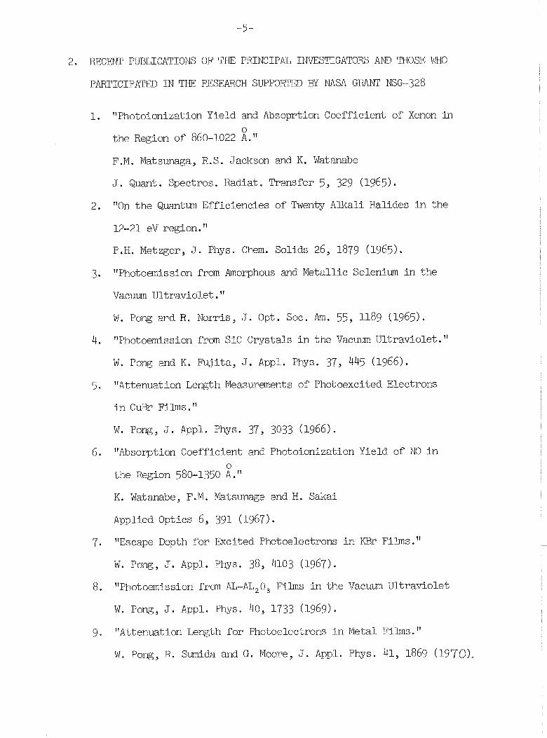
2. RE;CET\BT PUBLICATIONS OF THE PRINCIPAL ImSTIGATORS AND TJ3OSE It830
PAFfPICIPAlTD I N THf3 RESEARCH SUPPOF?IED BY NASA GRAm NSG-328
"Photoionization Yield and Absoprtion Coefficient of Xenon in 0
the Region of 860-1022 A."
F.M. Matsunaga, R.S. Jackson and K. Watanabe
J . Quant . Spectros . Radiat . Transfer 5, 329 (1965) . "On the Quantum Efficiencies of Twenty Alkali Halides i n the
12-21 eV region. "
P.H. Metzger, J. Phys. Chem. Solids 26, 1879 (1965).
tfPhotoemission from Amorphous and Metallic Selenium i n the
Vacuum Ultraviolet . I f
W. Pong and R. Norris, J . Opt. Soc. A.n. 55, 1189 (1965).
"Photoemission from Sic Crystals i n the Vacuum Ultraviolet . "
W. Pong and K. Fuj i ta , J. Appl. Phys. 37, 445 (1966).
"Attenuation Length Measurements of Photoexcited Electrons
i n CuBr Films. "
W. Pong, J. Appl. Phys. 37, 3033 (1966).
"Absorption Coefficient and Photoionization Yield of NO i n 0
the Region 580-1350 A ." K. FJatanabe, F.M. Matsunaga and H. Sakai
Applied Optics 6, 391 (1967) . ItEscape Depth fo r Excited Photoelectrons i n KBr Films."
W. Pong, J. Appl. Phys. 38, 4103 (1967).
"Photoemission fran AL-AL,O, Films i n the Vacuum Ultraviolet
W. Pong, J . Appl. Phys. 40, 1733 (1969).
"Attenuation Length fo r Photoelectrons i n Metal Films."
W. Pong, R . Sumida and G. Moore, J . Appl. Phys. 41, 1869 (197Qj,,

3, ABSTRACTS OF PUBLICATIONS
1. "Photoionization Yield and Absorption Coefficient of 0
Xenon in the Region of 860-122 A."
Abstract--Absorption coefficient and absolute photo-
ionization yield of xenon gas have been measured by 0
photoelectric methods with 0.2 A bandwidth in the 0
860-1022 A region. Ionization yields were obtained
with a platinum detector calibrated against a cali-
brated thermocouple. A yield value of unity was ob-
tained throughout this region which includes preionized
Rydbery lines. The absorption coefficient at most
wavelengths fell between the spread of previous values.
2. "On the Quantum Efficiencies of Twenty Alkali Halides
in the 12-21 eV Region."
Abstract--Absolute photoelectric yields of twenty
alkali halides have been measured, using a rare gas
ion chamber to determine the flux distribution of the
He2 continuum between 12.4 and 21.2 eV. In addition,
semiquantitative absorption coefficients were obtained 0
by evaporating AX (alkali halide) films on 300 A thick
A120, windows. For most of these materials the photo-
electric yield rises to values as high as 0.8 electron/
incident photon in the fundamental band beyond the
stable exciton region. At photon energies near twice
the threshold (or approximately 2 ET) the yield often

reaches a distinct minimum of the order of 0.4 elec-
tron/incident photon. This region is likely charac-
teristic of double exciton production. Beyond 2 ET
the yleld generally rises to very large values, even
over 1.0, strongly implying double excitation processes.
Many broad diffuse bands, sometimes well correlated
with the absorption coefficients, appear in the elec-
tron emission spectrum.
"Photoemission from Amorphous and Metallic Selenium
in the Vacuum Ultraviolet."
Abstract--Photoelectric yields of amorphous and metallic
selenium films were measured over the spectral range of 0
2000 to 1100 A. No appreciable difference between the
yields (number of electrons per incident photon) of the
two forms was observed. However, the retarding poten-
tial data show that the emitted photoelectrons from
metallic Se are distributed over a slightly higher
energy range than those from the amorphous form. The
results can be explained on the basis of the energy
band model of Se.
4. "Photoemission from Sic Crystals in the Vacuum Ultra-
violet. " Abstract--The results of quantum yield measurements on
p and n type Sic crystals of hexagonal structure are
in agreement with the theoretical expectation that p-

type samples should exhibit a higher quantum yield
than n-type samples. The higher yield of the p-type
crystal can be accounted for by assuming the existence
of space-charge band bending at the surface.
5. "Attenuation Length Measurements of Photoexcited
Electrons in CuBr Films."
Abstract--The attenuation length of photoexcited elec-
trons in evaporated layers of CuBr was estimated by
measuring the photoemission yield as a function of
thickness. The attenuation length was found to be
less than the optical absorption depth at photon
energies between 8 and 11 eV. At hv=9.7 eV, the 0
attenuation length is approximately 51 A.
6. "Absorption Coefficient and Photoionization Yield of 0
NO in the Region 580-1350 A."
Abstract--Photoionization yield and absorption co-
efficient of nitric oxide were measured at many wave- 0
lengths in the region 580-1350 A. H2 emission and
helium continuum sources were used with a 1-m mono-
chromator. Absolute intensity measurements were based
on a calibrated thermocouple.
7 . "Escape Depth for Excited Photoelectrons in KBr Films."
Abstract--We have investigated the backward photo-
emission from KBr films as a function of film thickness.

The attenuation length for electrons excited by pho- 0
tons of 10.2 eV was found to be about 180 A, which
is slightly greater than the absorption length for
photons in KBr. The mean free path for electron-
phonon collisions at 300'~ was estimated to be approx- 0
imately 42 A.
8. "Photoemission from AL-AL203 Films in the Vacuum Ultra-
violet Region."
Abstract--Measurements of quantum yield of A1-A120,
films were made at photon energies between 7 and 22 eV.
The photoelectric threshold for intrinsic photoemission
from amorphous A1,03 appeared to be about 8 eV. Approx-
imately 1 eV was estimated for the electron affinity of
A1203. The yield of anodic oxide film on aluminum at
10.2 eV decreased with increasing oxide thickness while
the yield at 21.2 eV increased. The decrease in yield
at 10.2 eV was attributed to photoelectrons originating
from the aluminum film beneath the oxide layer. Attempts
were made to study the escape probab~lity function for
electrons moving through the oxide into the vacuum. An u
attenuation length of about 130 A for the photoelectrons
in the oxide was obtained by using the exponential-
function approximation. The maximum initial energy of
the electrons was estimated to be 7.8 eV above the vacuum
level. The electron mean free path for electron-phonon
collisions in the oxide was estimated to be app~oximately

sixteen angstroms. In the analysis of the mean free
path, the emission of one phonon of 0.1 eV was assumed
in each energy-loss collision.
9. "Attenuation Length for Photoelectrons in Metal Films."
Abstract--Photoelectric yields of evaporated gold and
aluminum films of various thicknesses were measured
in the photon-energy region of 7.7 to 11 eV. From the
analysis of the yield data, the attenuation length for
the excited photoelectrons was estimated. For elec-
trons excited by photons of 10.2 eV, the attenuation
length for photoelectrons in aluminum is about five
times as large as that for electrons in gold. By us-
ing the Kane model for collision effect in photo-
emission, we were able to show that the attenuation
length obtained from our yield data for aluminum is
consistent with the photoelectron mean free path values
reported by Stuart and Wooten [Phys. Rev. 156, 364
(1967) 1.

4 . CALIBRATION OF THERMOCOUPLE AND SECONDARY DETECTORS
FOR ABSOLUTE INTENSITY MEASUREMENTS IN THE VACUUM
ULTRAVIOLET.
4.1 Introduction
For reliable measurements of photon flux, it is
necessary to use a radiation detector whose calibrated
quantum efficiency remains constant with time and
changes in vacuum conditions. In vacuum ultraviolet
work, it is convenient to measure the incident inten-
sity by means of windowless photoelectric detectors.
Certain metals such as tungsten, platinum, and gold
have been used as photocathodes. These metals have
been found to be suitable secondary standards for 0
intensity measurements below 2000 A. They appear to
be stable inasmuch as their quantum efficiencies are
reproducible.
The absolute quantum yield of a photocathode can
be determined by measuring the photoemission current,
provided the incident photon flux is known. We define
the quantum yield Y by the ratio of the number of
electrons emitted per second to the number of incident
photons per second. Accordingly, we write
Y = number of electrons/number of photons. (1)
Thus if the yield is known, the photoemission current
can be related to the incident photon flux. If the
spectral quantum yield is used to determine the photo-
electric threshold of a material, it is desirable to
define the quantum yield YA by the ratio of the number
of electrons emitted per second to the number of pho-
tons absorbed per second. If the photocathode mate-
rial is sufficiently thick and the reflectance R is
given, we can relate Y to Y by A
4.2 Thermocouple Calibration
Previous work has shown that the intensity of
incident photons in the vacuum ultraviolet region
can be measured by the use of a thermocouple. 5 , 16
As described in our 1964-report on intensity measure-
ments, a windowless Reeder compensated thermocouple
with a detector area of 1 mm x 3 mm was used. Simi-
lar thermocouples were employed in other experiments
in our laboratory. Each thermocouple was calibrated
in air against a standard lamp from the National
Bureau of Standards according to the recommended pro-
cedure. l7 Since the thermocouple for our experiments
must operate in a vacuum chamber, the vaccum-to-air
ratio was measured in order to determine the actual
sensitivity under operating conditions. The sensiti-
vity values of the thermocouples calibrated in our
laboratory varied from 2,04 to 6 , 7 3 microvolts per
microwatt. The output response was measured by a
breaker amplifier (Beckman Model 14) and a chart
paper recorder.
The possible sources of error in our thermo-
couple calibration have been discussed .'( A more
detailed study of the Reeder thermocouple charac-
teristics has been reported by Johnston and Madden. 18
Figure 1 illustrates a typical application of our
thermocouple in measuring photon flux passing through
the exit slit of a vacuum ultraviolet monochromator.
4.3 Absolute Quantum Yield of Metal-Foil Photocathodes
In our earlier work, the absolute quantum yields
of some metals and semiconductors were measured in the 0
spectral region 900 - 2000 A by means of a calibrated thermocouple. Since these measurements were made
with the samples in a vacuum of about lo-' Torr, the
results may not be the same as those obtained with a
better vacuum. In our recent work, the yield measure- 0
ments in the region 2000 - 1100 A were performed with
the sample in a vacuum of - loM8 Torr. The expe-
rimental chamber with a sealed LiF window was initially
evacuated by a sorption pump and then continuously by
an ion pump (80 L/s). All removable parts of the vac-
uum system were assembled with copper gaskets. In our
high vacuum measurements, a gold foil was employed as
a sec.ondary standard. Figure 2 illustrates the spectral

quantum y i e l d of t h e go ld f o i l . The metal f o i l was
purchased from t h e J a r r e l l -Ash Company. 0
I n t h e s p e c t r a l r e g i o n between 537 and 1216 A,
we used a t ungs t en f o i l a s a secondary s t anda rd t o
determine t h e a b s o l u t e i n t e n s i t y of t h e i n c i d e n t r a - 0
d i a t i o n . The y i e l d of t h e f o i l a t wavelength 584 A
was i n i t i a l l y determined a t t h e Fa r UV Radia t ion
Laboratory-National Bureau of S t anda rds . 2 0 The y i e l d
o f t h e same tungs t en f o i l was a l s o measured wi th t h e
c a l i b r a t e d thermocouple used i n our l a b o r a t o r y . The 0
y i e l d va lues a t wavelength 584 A ag ree w i t h i n t h e e s -
t ima ted exper imenta l e r r o r of F 5 % . The c a l i b r a t e d 0
y i e l d a t 584 A i s be l i eved t o be most r e l i a b l e be-
cause t h e e f f e c t of s c a t t e r e d l i g h t i s n e g l i g i b l e i n
t h i s s p e c t r a l r e g i o n . The y i e l d va lues a t o t h e r wave-
l e n g t h s were determined by comparing t h e photoemission
c u r r e n t s w i th t h e photoluminescent response of sodium
s a l i c y l a t e . 21' 22 Figure 3 i l l u s t r a t e s t h e s p e c t r a l
quantum y i e l d of t h e t ungs t en f o i l .

PHOTOEMISSION FROM METALLIC FILMS
Although the photoelectric effect was discovered
many years ago, the detailed consideration of the
photoemission process is still an area of basic re-
search in contemporary physics. Since a photon con-
tributes only negligible momentum in the optical exci-
tation of electrons in a crystal, the excited electron
must obtain momentum from the surface potential barrier
or from the periodic potential inside the crystal. Con-
sequently the question arises as to whether the surface
or volume effect is the predominant mechanism. This
problem has been discussed in the literature. 2 3 - 2 5
According to recent experimental evidence, photoemission
from solids is primarily a volume effect. 2 6
5.1 Quantitative Theory (One-Dimensional Model)
If we consider photoemission as a volume effect, it
is useful to consider the mechanism in three steps: 1)
absorption of a photon by an electron in the solid; 2)
motion of the photoexcited electron to the solid-vacuum
interface; 3) escape of the photoelectron over the sur-
face barrier into the vacuum. This model appears to be
adequate in explaining the quantum yields of metals.
However, it has been suggested that it might be more
appropriate to treat optical excitation, scattering, and
the escape across the surface as a one-step process . 2 7 s 28
For simplicity, we will employ the three-step model to

explain the results of our experiments.
In order to calculate the quantum yield of a
photoemissive material, we need to know the escape
probability function for the electron optically ex-
cited at some distance x beneath the surface. A model
has been developed to determine the probability of
escape. 2 9 In this model, we introduce a mean free
path R for electron-phonon scattering; a mean free P
path R e for electron-electron scattering; and a prob-
ability r that the photoelectron is reflected from
the solid-vacuum interfact at x = 0 . We will assume
that the scattered photoelectron and the secondary
electron produced in the electron-electron collision
are not sufficiently energetic to escape into the
vacuum. That is to say, both electrons are scattered
into states below the vacuum level. This assumption
is probably valid unless the surface work function or
the electron affinity of the solid is greatly reduced
by a thin surface layer of low work-function material
such as cesium. We will also assume that the mean free
paths are independent of the phonon energy loss. The
phonon energy loss per collision is considered to be
negligible.
If scattering is primarily due to electron-phonon
and electron-electron collisions, we can derive an ex-
pression for the escape length in terms of the mean
free paths for collisions. First of all, we specify

t h a t t h e p r o b a b i l i t y t h a t t h e e l e c t r o n w i l l make an
electron-phonon c o l l i s i o n a f t e r t r a v e l i n g through a
d i s t a n c e Ax i s Ax/R . The p r o b a b i l i t y t h a t t h e e l e c - P
t r o n w i l l make an e l e c t r o n - e l e c t r o n c o l l i s i o n a f t e r
t r a v e l i n g through t h e d i s t a n c e Ax i s Ax/&,. If
x = N Ax, t h e p r o b a b i l i t y t h a t t h e e l e c t r o n w i l l no t
make any c o l l i s i o n i n t r a v e l i n g a d i s t a n c e x i s
We can s i m p l i f y t h i s exp re s s ion by l e t t i n g N become
l a r g e and Ax become sma l l . Accordingly, we can w r i t e
g ( x ) = emcX, (2) -1 -1
where c = R P + 'e
. With t h i s r e l a t i o n s h i p e s t ab -
l i s h e d , we s p e c i f y t h e p r o b a b i l i t y t h a t an e l e c t r o n
e x c i t e d a t x t r a v e l s t o t h e s u r f a c e and escapes from
t h e s u r f a c e i s
The f a c t o r % accounts f o r t h e f a c t t h a t it i s e q u a l l y
l i k e l y f o r t h e e l e c t r o n t o move towards t h e s u r f a c e
o r away from i t .
Now suppose an e l e c t r o n i s o p t i c a l l y e x c i t e d a t x
beneath t h e s u r f a c e and a r r i v e s a t p o s i t i o n s wi thout
making any c o l l i s i o n , where s = 0 i s t h e s u r f a c e . The
p r o b a b i l i t y t h a t i t w i l l i n t e r a c t w i th a phonon a t s
i s ds/R - Af te r t h e f i r s t c o l l i s i o n , t h e p r o b a b i l i t y P -
t h a t t h e e l e c t r o n a t s w i l l escape a f t e r (n-1) e l e c t r o n -

phonon collisions is pn-l(s). As shown in Fig. 4,
there are three ways of getting to position s before
the first collision. Letting pn(x) be the probability
that an electron will escape from the surface after
making n electron-phonon collisions, we write
The total probability of escape is
Since 00
n=l we find
1 -C (x-s ) -C (x+s ) ds +

Differentiation with respect to x results in
For a semi-infinite medium, the solution is
1
where L-I = (c2 - ~ 2 - l ) ~ . The constant B can be P
evaluated by substitution in Eq. (6). The parameter
L is called the escape length or attenuation length
for the photoelectron.
Equation (8) appears to be a good approximation
for the probability of escape. It has been used
successfully in explaining the essential features of
photoemission yields. 30 Furthermore, the escape prob-
ability function of the form similar to Eq. (8) has
been found to be satisfactory in the theoretical treat-
ment of secondary emission. 31
Since the escape length or attenuation length L
is related to the mean free paths for collisions, it
should be of interest to see how the mean free paths
can be calculated from the fundamental theory of elec-
tron scattering in solids. A brief discussion of the
important scattering processes is given in the follow-
ing sections.

Electron-phonon Scattering
The mean free path ep can be related to the
energy band structure of the photoemissive material.
3 2 According to Kane , Rp can be calculated from the
expression
where v is the group velocity of the photoelectron, Q
and wp is the transition probability per unit time
for electron-phonon interaction. Applying the Golden
Rule of time-dependent perturbation theory, 33 we can
write
where wp represents the phonon scattering rate, and
p ( E ) is the density of final unperturbed states. The
quantity M~ is assumed to be approximately constant.
The group velocity v can be calculated for a given l3
energy band structure E ( k ) , i.e.,
Electron-electron Scattering
The mean free path for electron-electron collisions
can be calculated from

where we denotes the scattering rate due to electron-
electron interaction. Using the Golden Rule, we write
where the matrix element M can be calculated from the
screened Coulomb interaction including exchange.
The inelastic scattering mechanism due to electron-
electron collisions has been studied also by Berglund
and ~ ~ i c e r 3 ~ . Following the approach used by Motizuki
and they considered the situation in which
the photoelectron in state (Et, k l ) is scattered to
state (E, k) while the interacting electron is scattered
from state (E,, k,) to state (El, kl). The probability
per unit time for this to occur is given by
where He, is the perturbation Hamiltonian for electron-
electron interaction. In the work of Motizuki and Sparks,
a phenomenological Yukawa potential of the form
was assumed for the interaction potential function. In
order to find the total probability per unit time of an
electron of energy E' being scattered to any energy E,
Eq. (14) must be summed over all possible states corres-
ponding to k', k,, k, kl, E, El, and E,. This can be
done if the wave functions are known.

Since accurate information on wave functions
may not be available, it is worthwhile to note that
approximations can be made in evaluating the total
probability per unit time of an electron with energy
E T being scattered to any energy E. In the study of
photoemission from metals, Berglund and Spicer 34
have demonstrated that it is a good first order
approximation to assume that the matrix element in
Eq. (14) is independent of the k vectors of the
electrons involved. By using the appropriate den-
sities of states and Fermi functions, they pointed
out that the total probability per unit time can be
written as w w
It should be noted that Pt(E1) is the reciprocal of the
lifetime for electron-electron scattering of the photo-
electron with energy E T . Therefore the mean free path
R e can be expressed by
It should be mentioned that the mean free path R e
for electrons in a metal has been calculated by &uind6.
He used the dielectric constant approach in which the
conduction electrons were assumed to be a degenerate
electron gas. For low energies, the mean free path
R e is given by
Re N 9 (17) [ t an - ' (n/ar,)t + r ) ( I + ars/r)]
where E, is the Fermi energy; a ( 4 / 9 1 ~ ) ~ ' ~ , and r,
is the radius (measured in units of the Bohr radius
a,) of a sphere equal in volume to the volume per
electron. Eq. (17) represents the distance that an
excited electron travels in going from an initial
excitation energy E to a final excitation energy tf. i
To satisfy our definition of R e , we make tf equal
to the work functfon of the metal. This distance is
measured along the path of the excited electron. No
random-walk situation is assumed in the calculations.
Quinn has pointed out that the average energy lost
by an excited electron in a typical electron-electron
collision is not small compared to its initial exci-
tation energy.
In order to obtain a theoretical estimate of
the scattering lengths for electrons in metals, we
used Eq. (17) to find R e for aluminum and gold. The
following examples illustrate the theoretical esti-
mates of the electron-electron scattering lengths for
the same initial excitation energy.

Examples :
For excited electrons in aluminum (r, s 2,
Eo x 12 eV, ti FY 10 eV, f f FZ 4.2 eV), we have 0
Re % 50 A. For electrons in gold, (r, z 3,
E, z 5.5 eV, Ei=10 eV, tf a4.7 eV), we find 0
R e x 7 A.
Improvements in calculating the electron-
electron mean free path were subsequently made by
considering the effect of virtual transitions, band
structure, and exchange processes. 37-39 If these
corrections are taken into account, the calculated
mean free path is somewhat larger than that pre-
dicted by the free electron gas model.
Electron-Plasmon Scattering
In some metals, the excited photoelectron may
be sufficiently energetic to interact with the plasma
oscillations of the electrons in the metal. It is
well known that the energy loss due to plasmon crea-
tion depends on the concentration of free electrons
in the metal. 40 It is possible to generate both
volume and surface plasmons. This type of inelastic
scattering should be considered if high-energy photo-
electrons are involved. Examples of volume plasmon
energies are 5.7 eV for sodium, and 15.3 eV for alu-
minum. The surface plasmons have lower energies.
Auger Process
If an electron is optically excited from a low-
energy state of energy El, another electron from an
upper state of energy E2 may occupy the state of
energy El. The energy released from this transition
may be absorbed by a third electron situated at some
energy level E above El. The third electron excited 3
to a state E (above the Fermi level), where E-E3=E2-El,
is called an Auger electron. 34 If the Auger electron
is sufficiently energetic, it may escape into the
vacuum. Thus the onset of the Auger process can give
rise to a higher quantum yield.
5.2 Experimental Study of Photoemission from Metal Films.
As shown in Fig. 5, photocathodes may be fabri-
cated for applications with radiation incident from
the vacuum interface from which photoelectrons are
emitted or from the substrate interface. The "front"
illumination refers to the situation indicated in
Fig. 5a; the "back" illumination is the situation
indicated by Fig. 5b. The case of "back" illumination
is of practical interesta4 It is obvious that "back"
illumination requires semitransparent photocathodes,
in which case the optimum quantum yield depends on
the thickness of the photoemissive film.
The principal aim of our experimental study on
metal films has been to measure the quantum yields
for "back" illumination as a function of film thick-
ness in the spectral region above 1100 8. Polished LiF crystals were used as substrates for the evapo-
rated metal films. The experimental information
should be of considerable interest to those who are
directly concerned with the development of photo-
electric detectors with LiF windows. In addition to
the practical value of the results, the yield versus
thickness data can be used to determine the attenua-
tion length for photoelectrons.
5.3 Attenuation Length for Photoelectrons in Metal Films.
Photoemission from Gold and Aluminum Films
Scattering of electrons in metal films is of
current interest because the hot-electron transport
process in thin-film devices does not appear to be
well understood. 41
Some experimental studies 4 2 - 4 5
have been made to determine the mean free path for
excited electrons in metals, but very little work
has been done to extend the investigation to elec-
trons excited by vacuum ultraviolet radiation. The
purpose of our experiments has been to investigate
the attenuation of vacuum uv photoexcited electrons
in evaporated metal films.

The important scattePYng mechanisms in a solid
film are assumed to be electron-electron and electron-
phonon collisions. The combined effect of these
collisions on the excited electrons can be expressed
in terms of the attenuation length. As shown in a
simple model for collision effects in photoelectron
emission, 2 9 , 46 the attenuation length L is related
to the escape probability by
where x is the distance between the surface and the
point at which the electron is excited; B is the
escape probability for the electron excited at the
surface. The escape probability function is useful
in calculating the photoelectric yield of a photo-
emissive material. The photoelectric yield described
in the present work is defined as the number of elec-
trons emitted per incident photon.
As described in our previous studies, 1 3 , 1 4 the
electrons in a thin film can be excited by photons
which pass through the LiF substrate. In the present
study, the metal films were deposited on polished LiF
crystals of 25 rnrn diameter and 2 mm thick. The crys-
tal was mounted near the exit slit of a vacuum uv
monochromator. For electrical contact with the evapo-
rated film, a gold film was previously deposited on
the LiF surface adjacent to the substrate areas for

the evaporated films. It was possible to deposit
three films on the crystal, each on a different
section of the crystal surface. As shown in Fig. 6,
the position of the crystal could be changed by
means of a linear-motion feedthrough. Photoemission
measurements were made immediately after evaporation
at a pressure of approximately low7 Torr. Sorption
and ion pumps were used to evacuate the photocell
and evaporator chamber.
The thickness of the evaporated film was deter-
mined by comparing the measured transmittance with
the transmittance calculated as a function of film
thickness for photons of 10.2 eV. The effect of
interference due to multiple reflections was taken
into account in computing the transmittance of the
metal film. Figures 7 and 8 illustrate the calcu-
lated transmittance and reflectance as a function of
film thickness for gold and aluminum at 10.2 eV.
Particular attention was given to gold and aluminum
because the values of the optical constants of these
metal films in the vacuum uv region can be found in
the literature. 47-49 The photon flux which passed
through the LiF substrate was measured by a calibrated
gold-foil photoelectric detector. The typical value
of the photon flux of 10.2 eV was approximately 4 x 10 9
photons per second. The size of the incident light
beam at the crystal surface was 1 mm x 3 mm.

The photoemission currents at a number of wave- 0 0
lengths between 1608 A and 1117 A were measured as
a function of time after the film was deposited on
the substrate. A noticeable change of photoelectric
yield with time immediately after evaporation was
observed. It was particularly noticeable for alumi-
num. The yield at photon energies below 9 eV de-
creased while the yield above 9.7 eV increased with
time. The maximum change of yield over a period of
60 minutes after evaporation was about 33 percent
for aluminum at 11 eV. The change of yield with
time may be attributed to absorbed atoms or mole-
cules on the metal-vacuum surface. With the assump-
tion that the change of yield with time was due to
surface contamination or oxidation, 5 0 the yield of
the clean metal film was obtained by extrapolating
the yield versus time curve to zero time. Figures
9 and 10 illustrate the extrapolated yields of several
films of different thicknesses for evaporated gold and
aluminum. It should be mentioned that the change of
yield with time after evaporation of aluminum in a
vacuum of 5 x 10 -lo Torr has been observed. 51 This
suggests that the coverage of the surface by atoms of
the residual gas may not be the only cause of the ob-
served change of photoemission yield.
In order to find the attenuation length for the
photoelectrons from the experimental data, we compared

the measured yield with the calculated yield. If
we use the escape probability function described by
Eq. (I), we can express the yield for photoemission
from the backside of a film of thickness t as
where a is the absorption coefficient; R, the reflect-
ance; Io3 the number of incident photons per second.
Upon evaluating the integral in Eq. (2), we get
Y = BaL (1 - R) - e -t/L)/(l - a~).
It is assumed that the value of L in Eq. (3) is chay-
acteristic of the average energy of the electrons
initially excited by the photons. A smaller L value
is expected for a higher average energy. We can es-
timate the value of L by comparing the measured yield
as a function of film thiclcness with the yield cal-
culated from Eq. (3). An example of this comparison
is shown in Fig. 11. The values of B and L were se-
lected to fit the yield data. The L values for the
photoelectrons excited at different photon energies
are shown in Fig. 12. The results indicate that the
attenuation length for electrons in aluminum is about
five times as large as that for electrons in gold at
10.2 eV. The lack of strong dependence on the photon
energy in this region suggests that a relatively large
fraction of low-energy photoelectrons can still be

excited initially by photons of higher energies.
In order to compare the attenuation-length value
obtained from our experiments with the scattering
lengths reported by Stuart and ~ o o t e n ~ ~ , we used the
expression derived by ~ a n e ~ 9 , which relates the atten-
uation length to the mean free path Re for electron-
electron collisions and the mean free path Rp for
electron-phonon collisions. This expression is given
by
The values of the mean free paths obtained by Stuart 0 0
and Wooten were Rp - 130 A and Re - 500 A for elec- trons excited by photons of 9.2 eV in aluminum. If
these values are used in Eq. (4), the attenuation 0
length would be approximately 230 A, which is in good
agreement with the value obtained from our yield data.
Scattering-length measurements based on electron-
beam attenuation were reported recently by ~ a n t e r ~ ~ .
For electrons in gold, the values (Re - 45 X and 0
Rp - 250 A) are in agreement with our data. However,
for electrons in aluminum, the values (Re - 50 # and 0
R~ - 250 A near 5 eV above the Fermi level) are in 5 2 disagreement with the results of Stuart and Wooten .
From our point of view, the values from Kanter's
measurements do not give the same attenuation-length
value obtained from our data for electrons in aluminum.

It should be noted that Kanter9s definition of attenua-
tion length is different from the one used in photo-
emission studies. In Kanterls work, the relationship
between attenuation length and the mean free path is
given by
In our work, the attenuation length or escape length
is defined in terms of the escape probability q(x) =
B exp (-x/L), where L is related to the mean free
paths described in Kane's model. The two L values
agree only if R is much larger than R . P e
Photoemission from Nickel Films
Previous measurements of photoemission from
evaporated nickel films have stimulated much interest
concerning the density of states of nickel. Energy
distribution measurement^^^ of the emitted electrons from nickel indicated a strong peak in the optical
density of states at approximately 4.5 eV below the
Fermi level. In disagreement with this result were
soft x-ray studies55 and ion neutralization spectros-
copy work56 which showed a dominant peak in the den-
sity of states within 2 eV of the Fermi level. Fur-
thermore, the anomalous peak was not in agreement
with the results of one-electron band calculations
for nickel. Recently, the question was resolved by
57 further photoemission studies which showed that the
anomalous peak was sensitive to the surface condition
of nickel. The surface contamination of nickel films
58 at 3 x Torr was also reported by Vehse and Arakawa . It appears that energy distribution measurements
are extremely sensitive to the surface conditions of
some metals. Eastman and ~ r o l i k o w s k i ~ ~ pointed out
that the surface conditions of nickel are important
because the electron escape depths are very short.
They concluded that the scattering lengths for elec- 0
trons in nickel are about 5 to 15 A for energies
greater than 7 eV above the Fermi level. 0
If the escape depth is about 15 A, a very thin
film of nickel should have optimum yield. In an
effort to get a better understanding of the photo-
electric properties of very thin films, we prepared
nickel films on polished LiF crystals and measured
the yield immediately after evaporation. The film
thickness was estimated from transmission measurements 0
at wavelength 1216 A. The calculated transmittance of
a nickel film on a LiF substrate as a function of film
thickness is shown in Fig. 13. The spectral quantum
yields of nickel films of different thicknesses under
"back" illumination are illustrated in Fig. 14. The
fact that photoemission from a very thin nickel film
can be measured indicates that the evaporated film is
sufficiently continuous to provide electrical contact
with the metallic film electrode around the substrate
area. The spectral quantum yield of nickel under
"front" illumination by photons of energies between
10 and 23 eV is shown in Fig. 15. In our measure-
ments, we observed a gradual change of yield with
time immediately after evaporation at lom7 Torr. The
yield values shown in Fig. 15 are extrapolated yield
data at zero time for films of different thicknesses.
The gradual change of yield may be attributed to sur-
face contamination or a gradual change in film struc-
ture immediately after deposition. 51 The experimental
chamber for measuring photoemission in the spectral
region of 10 to 23 eV is shown in Fig. 16. The helium-
continuum light source and a one-meter normal incidence
monochromator were used to provide the dispersed radia-
tion.
A few remarks in regard to the quantum yield of
nickel films should be made. No significant change in 0
yield with increasing film thickness larger than 20 A
under "front" illumination was observed. The yield of 0
very thin films (less than 20 A according to trans-
mittance measurements) is somewhat higher than the
yield of thicker films. The lack of increase in yield 0
with increasing film thickness greater than 20 A under
"front" illumination suggests that the electron escape 0
length is less than 20 A. This estimate is in agree-
ment with the results of Eastman and ~ r o l i k o w s k i ~ ~ .

The slightly higher yield of the thin films might be
due to backscattering from the substrate interface.
The yield in the region 10 to 23 eV can be cal-
culated for a sufficiently thick film of nickel. Since
the escape length is small in comparison with the ab-
sorption depth, the expression for the quantum yield
should be proportional to (1-R)aj where a is the ab-
sorption coefficient and R is the reflectance. Figure
17 illustrates (1-R)a as a function of photon energy.
Comparing the shape of the yield curve with the spec-
tral values of (1-R)aj we find they are in qualitative
agreement.
Photoemission from Beryllium Films
While optical studies on beryllium films in the
far ultraviolet region have been reported, 59 not much
work has been done to determine the photoelectric
yield of pure beryllium. For this reason, we performed
yield measurements on evaporated Be films in the spec-
tral region 10 to 23 eV.
Pure beryllium flakes purchased from the Johnson,
Matthey & Company were evaporated from a tantalum boat
to form a film on a polished LiF substrate. The thick-
ness of the film was estimated from transmittance meas-
urements at 10.2 eV. The transmittance and reflectance
as a function of film thickness at wavelength 1216 8

are shown in Fig. 18. A gradual change of yield with
time immediately after evaporation was observed at
Torr. The yield versus time curves were plotted and
the extrapolated yield at zero time was determined for
varjous photon energies.
Figure 19 illustrates the spectral quantum yield
of evaporated beryllium. Comparing the spectral yield
curve with the (1-R)a curve for Be, we see that the
spectral yield does not decrease as capidly as (1-R)a
for photon energies above 13 eV. The (1-R)a values
shown in Fig. 20 were calculated from the optical data
published in reference (59).

6. PHOTOEMISSION FROM SEMICONDUCTORS
When electrons are optica,lly excited from the
valence band of a semiconductor, the excited electron
may move to the surface and escape into the vacuum.
In the absence of band bending, the surface energy
barrier for the photoelectron is called the electron
affinity of the semiconductor. The electron affinity
EA represents the energy between the vacuum level and
the bottom of the conduction band.
The escape condition for the photoelectron is
where vx is the component of the electron velocity
along the direction normal to the surface. The prob-
ability of escape at the surface can be estimated by
considering the angle of incidence of the excited
electron upon arrival at the surface. If a photo-
electron of kinetic energy E relative to the bottom
of the conduction band approaches the surface at
angle 8 with respect to the normal, the escape con-
dition requires that
2 cos 0 > EA/E .
Hence the "escape" cone is limited by the angle

If the angle of incidence is greater than Om, the
photoelectron should be reflected back into the solid.
Assuming the probability that the excited elec-
tron of energy E moves in any direction is the same,
we can express the probability that it will approach
the surface at some angle between 8 and 8 + de by
d ~ / 4 ~ = % sin 8 d8 ,
dR is the element of solid angle. By integrating
Eq. (2) over the angle of the escape cone, we see
that the probability of escape at the surface is
given by
60,61 Equation (3) is useful in electron-emission studies.
For most semiconductors, the value of EA is not
larger than 5 eV. For most metals, the surface
barrier is about 10 eV, i.e., the Fermi energy plus
the work function. According to Eq. (3), the elec-
trons excited to states of energy E in most metals
would have a lower probability of escape at the surface
than the excited electrons of the same energy in semi-
conductors. However, photoemission is predominantly
a volume process; so the quantum yield depends on elec-
tron scattering processes beneath the surface in addi-
tion to the escape situation at the surface.

In a semiconductor, the photoelectron may lose
energy by making collisions with phonons, defects,
and electrons in the valence band. The inelastic
collisions which create additional free electrons
and holes are of particular interest in photoemission
studies. 6 2 3 63 Impact ionization (across the band
gap) is also an important mechanism of electrical
conduction in semiconductors. 64-66 Sommer and spicer67
have summarized the published information concerning
the threshold energy for electron-hole pair production
in various semiconductors. For most materials, the
threshold energy appears to be greater than 2Eg, where
Eg is the band-gap energy. This is an important rela-
tionship as far as photoemission is concerned. If the
electron affinity is not small and the band gap is not
sufficiently large, inelastic scattering involving im-
pact ionization would reduce the total probability of
escape for the excited electron in the semiconductor.
This type of interaction leads to small quantum yield.
On the other hand, if the electron affinity is small
and impact ionization occurs, the scattered photoelec-
trons and the secondary electrons may escape into the
vacuum and thereby give rise to high quantum yield.
The theoretical consideration of photoemission from
semiconductors near the threshold for a general band
structure has been discussed by ~ a n e ~ ~ . He showed that
the yield vs energy relation near the threshold can be

related to a number of possible optical excitation
and escape mechanisms involving volume and surface
states in semiconductors. In the presence of surface
states, band bending in semiconductors occurs. The
dominant effect of band bending is to raise or lower
the effective photoelectric threshold for the photo-
electrons originating from increasing depths below
the surface. 69, 70
6.1 Photoemission from Silicon
Silicon is a well known semiconductor. The
electrical properties of silicon are fairly well
understood. The optical constants of Si in the re-
71 gion 1 to 10 eV were measured by Philipp and Taft . Further measurements of the optical constants in the
region 10 to 19.2 eV were reported by Sasaki and
~ s h i ~ u r o ~ ~ . The optical data showed evidence that
plasma oscillation can be excited by photons of
approximately 17 eV. Photoemission studiesT3-75 on
silicon crystals in the region below 6 eV have been
76 performed. Recently, Callcott reported some work
on Si in the region 6 to 9.6 eV. While photoemission
studies have contributed important knowledge on the
band structure of silicon, information on the photo-
electric yield above 6 eV does not appear to have
been published. The principal aim of our work on

silicon has been to determine how much effect the
oxide layer has on the spectral quantum yield.
The silicon samples used in our experiments
were p-type silicon slices (14 mm diameter and 0.25 mm
thick) with (111) surfaces. The resistivity of the
crystals was approximately 15 ohm-cm. In our experi-
ments, a thin silicon crystal was heated to a tem-
perature of approximately 1200 OC in a tantalum foil
holder. The duration of the heat treatment was about
3 minutes in a vacuum of about 1 x Torr. The
quantum yield was measured before and after heating.
The results are illustrated in Fig. 21. It is in-
teresting to note that the effect of heating is the
reduction of quantum yield above 10 eV. The spectral
quantum yield of a heat-treated Si crystal from 7.5
to 23 eV is shown in Fig. 22.
Our tentative explanation of the change of yield
after heat treatment is that the untreated Si crystal
has a thin layer of silicon oxide on its surface.
Photoemission from the oxide layer under optical ex-
citation above 10 eV would contribute to a higher
yield of the crystal before heating. At 1200 OC, the
oxide layer could be removed from the surface. Con-
sequently, the yield of the heat treated silicon crys-
tal should be lower for photon energies above the
photoelectric threshold of silicon oxide. The results
shown in Fig. 21 suggest that the photoelectric threshold

of silicon oxide is approximately 10 eV. It would be
desirable to measure the spectral quantum yield of pure
silicon oxide to substantiate our conclusion.
The decrease in yield of silicon above 17 eV may
be an indication that the photoelectrons are scattered
by plasmons in the crystal. A lower quantum yield
would be expected if a large fraction of the excited
electrons are scattered to states below the vacuum
level.
6.2 Photoemission from Sic
Low-temperature optical absorption and lumines-
cence of pure Sic crystals have been investigated
extensively in recent years. 77 The breaks observed
in the transmission curve near the absorption edge
have been attributed to excitations of acoustic and
optic phonons. The luminescence at low temperature
can be explained on the basis of recombination of
an exciton bound to an unknown impurity (possibly
nitrogen).
It has been demonstrated that silicon carbide
crystals can be made p or n-type by doping the crys-
tal with aluminum or nitrogen atoms. 78 The black
crystals are p-type; the green crystals are n-type.
Previous investigations of photoemission from
Sic crystals were made in the spectral region below
11 eV. 11379 Our measurements showed that p-type SIC has

a higher yield than the n-type crystal. The difference
is probably due to space-charge band bending near the
surface of the crystal.
We have performed further yield measurements on
the p-type Sic crystal in the spectral region above
0 11 eV. Heat treatment at approximately 950 C for 5
minutes in a vacuum of about 1 x Torr can change
the quantum yield appreciably at higher photon ener-
gies. The spectral yields measured before and after
heating are shown in Fig. 23.
6.3 Photoemission from Se and Te.
The electrical and optical properties of sele-
nium and tellurium are of current interest. It has
been discovered that selenium and tellurium approach
a metallic state under high-pressure conditions. 8 0
There are various forms of selenium. Amorphous sele-
nium is selenium in a glassy state with no well de-
fined freezing point. This form of Se consists of
Se8 rings, along with a few atoms (5%) in a weak
nearest-neighbor trigonal symmetry. 81 The amorphous
form of Se can be obtained by vacuum evaporation.
The metallic form can be produced easily by heating
the amorphous form to about 75 OC. 82 Similar to the
structure of crystalline Se, tellurium exists in a
hexagonal chain structure. 83

Results of optical studies on selenium and tel-
lurium in the vacuum ultraviolet region have been 84-86 -1
reported. The energy-loss function -Im(&) , which can be calculated from the optical data,shows
peaks at 5.3 and 19 eV for amorphous Se; at 5.6 and
17 eV for Te. The peaks at 19 eV for Se and 17 eV
for Te have been attributed to creation of volume
87 plasmons . If the volume plasmons are indeed excited at
19 and 17 eV in Se and Te, inelastic scattering of
photoelectrons by plasmons would occur above a certain
photon energy. If this occurs, the spectral quantum
yield should decrease at photon energies above the
plasmon energy. In order to see this, we measured
the quantum yield of evaporated selenium and tellurium
in the spectral region 10 to 23 eV, using the helium-
continuum light source. Figures 24 and 25 illustrate
the results. The decrease of yield appears at the ex-
pected range of photon energy. While the spectral
yield curves are in agreement with the occurrence of
electron-plasmon scattering, the spectral absorption
' curves illustrated in Figs. 26 and 27 could also be
used to explain the decrease in yield with increasing
photon energy. That is to say, the absorption length
could be longer than the escape length for the photo-
electron.

In the spectral region below 10 eV, we used the
hydrogen-discharge tube as a light source for the
monochromator. When hydrogen is used, the sample
chamber should have a LiF window because hydrogen can
react with Se and form hydrogen selenide. Previous
yield measurements on Se agree with our present data
10 over the overlapping region 10 to 11 eV.
The spectral yield of evaporated Te for photon
energies below 11 eV is shown in Fig. 28. The meas-
urements were performed with a LiF windowed experi-
mental chamber.
6.4 Photoemission from Cuprous Halides
Cuprous halides are semiconductors whose energy
band gaps are approximately 3 eV. The crystals have
a zincblende structure below 643 O K . Results of
optical studies on cuprous halides in the spectral
88 region 3 to 10 eV have been reported by Cardona . According to luminescence studies , 89 the exciton-
band structure of CuI at low temperature was found
to be sensitive to the film thickness. The Stoke
shift was attributed to exciton diffusion.
Photoemission from copper iodide has been re-
ported. CuI photocathode is of particular
interest in photon-detector development because CuI
has the desirable spectral yield for vacuum u.v.

applications. LiF-windowed photomultiplier tubes with
CuI photocathode are now commercially available. 93
In order to develop a better understanding of the
photoelectric properties of cuprous halides, photo-
emission experiments were performed to determine the
density of states and electron attenuation length in
these compounds. 94313 In our experiments on evaporated
CuBr under "back1' illumination, the yield of the photo-
emissive layer on a LiF substrate was measured as a
function of film thickness. As shown in Fig. 29, the
spectral yield of CuBr was found to be sensitive to
the film thickness. It is interesting to note that
the spectral response can be adjusted by varying the
film thickness. Figure 30 illustrates the yield of
CuI as a function of film thickness under "back1' illu-
mination of 10.2 eV. The film thickness was estimated
from transmittance measurements. The results show
that the optimum quantum yield of CuI at 10.2 eV is u
obtained for a film of approximately 50 A thick.
Previous yield measurement s9 on cuprous halides
were limited to the wavelength region above the LiF
cut-off. In order to determine the yield above 11 eV,
a windowless experimental chamber was used to perform
the measurements. The sample chamber and evaporator
were evacuated by a LN baffled 4-in oil diffusion
pump. The sample powders were purified by distilla-
tions in vacuum before being placed in a quartz boat

for evaporation in the experimental chamber. The
film was deposited on a polished LiF substrate. The
cuprous halide film made electrical contact with a
gold or silver film electrode which was previously
deposited on the LiF surface adjacent to the sub-
strate area. The purpose of the LiF substrate was
to provide sufficient transmittance of U.V. radiation
for estimating the thickness of the film. The helium-
continuum light source was used with the monochromator
to provide radiation of wavelengths between 1216 and 0
537 A. Hydrogen-discharge was employed for the longer
wavelength region.
Figure 31 illustrates the spectral yield of evap-
orated cuprous iodide under "f~ont" illumination. A
broad peak with its maximum near 12 eV may be related
94 to the optical excitations from the d band of copper . The yield over the spectral region 11 to 21 eV appears
to be relatively uniform.
6.5 Photoemission from Evaporated CdTe.
CdTe is a semiconductor whose band gap is 1.45 eV.
The electron affinity is approximately 4.5 eV. CdTe
has received a great deal of attention in recent years
because CdTe films deposited obliquely exhibit a large
photovoltaic effect. 96 The technique of preparing good
CdTe films has been discussed by a number of workers 9 7 , 9 8
It has been shown that pure CdTe films can be pro-
duced by vacuum deposition if the substrate tem-
perature is kept slightly above 300'~.
Photoemission from CdTe crystals has been
investigated by Scheer and van ~ a a r ~ ~ , and by Shay
and ~~icer'~~. In the Shay and Spicer experiments,
the photoemission measurements were made on cleaved
CdTe single crystals in ultrahigh vacuum. From the
energy-distribution measurements of the photoemitted
electrons, they were able to determine the absolute
energies of the initial and final states for the ob-
served optical transitions. Their estimate of the
widkh of the valence band is about 3.7 eV. Further-
more, their yield measurements below 11 eV showed
a gradual rise in yield in the region above 9 eV.
The rise in yield was attributed to the escape of
secondary electrons.
In order to determine whether electron-hole
pair production contributes to a higher yield with
increasing photon energy, we extended the yield
measurements to energies above 11 eV. In our ex-
periment, the pure CdTe film was prepared by evapo-
rating CdTe powder from a resistance-heated tantalum
boat onto a hot tantalum foil. The yield of the
evaporated film was measured at room temperature.
As shown in Pig. 32, the spectral yield of CdTe

appears to be similar to that of evaporated tellurium
in the photon-energy region above 10 eV.
6.6 Photoemission from Evaporated GaAs
The photoelectric properties of GaAs crystals
have been investigated recently. lo1-'03 The band-
gap energy is 1.4 eV. The photoelectric threshold
is approximately 5.5 eV. The quantum yield for
photon energies between 5.5 and 11 eV has been meas-
ured. Similar to CdTe, the ratio of the band gap
to the electron affinity is low. Therefore, low
quantum yield would be expected.
In previous work, a clean surface of GaAs was
obtained by cleaving a single crystal in ultrahigh
vacuum. While single crystals are suitable for
photoemission studies of band structure and electron-
transport properties of the they are
not as useful as the thin films which are required
for photoelectric applications. Unfortunately, it is
difficult to produce a pure GaAs film by conventional
vacuum evaporation. GaAs will decompose when the Sam-
ple is heated slowly. However, it has been reported
that an epitaxial film of GaAs can be deposited on a
hot germanium-crystal surface by flash evaporation. 106,107
The substrate temperature should be in the range of 400
to 6on0c=

In our experiment, the GaAs film was prepared by
the flash-evaporation method. The GaAs powder was
purchased from Semi-Elements, Inc., Saxonburg, Pa.
The substrate was a thin Ge crystal with surface (111).
The crystal was mounted in a tantalum-foil holder,
which also served as the substrate heater. The spec-
tral yield of a GaAs film on a Ge substrate is shown
in F1ig. 33. A broad peak appears near 14 eV. Since
the film thickness was not measured, we are not certain
that the observed yield is optimum for GaAs.
There is another technique of preparing GaAs films.
It involves separate gallium and arsenic evaporation
sources. Steinberg [Appl. Phys. Letters 12, 63 (1968)l
has shown that cesiated GaAs films can be prepared in
this manner for photoelectric applications.

7. PHOTOEMISSION FROM LARGE BAND-GAP SOLIDS
Large ba-nd-gap materials with low electron
affinity have photoelectric properties which are
desirable for vacuum U.V. applications. The useful
characteristics are high photoelectric threshold and
high quantum yield. Large band-gap materials are
suitable for use as photocathodes of "solar blind1'
photon detectors.
The high yield of a large band-gap solid with
low electron affinity can be understood readily by
considering the scattering processes for the excited
electrons in the solid. If the band gap is large,
inelastic scattering by the valence-band electrons
should not occur in the vacuum U.V. region. There-
fore, the scattering of the photoelectron is limited
to electron-phonon and electron-defect collisions.
Since the energy loss associated with these collisions
is small, most of the excited electrons arriving at
the solid-vacuum interface would still be sufficiently
energetic to escape into the vacuum.
The motivation for further photoelectric studies
of large band-gap solids is that optical excitations
and electron-transport properties of insulating solids
are not fully understood. It has been suggested that
exciton states of alkali halides are likely to be pres-
ent above the band-gap energy. lo8 Some photoemission

data appear to be compatible with this viewpoint. If
the continuum-state exciton can move through some dis-
tance before dissociating into a free electron-hole
pair, the attenuation length for a photoelectron could
be longer than the free-electron attenuation length of
the same energy. Evidence of relatively long escape
length for photoelectrons in alkali halide films has
been reported. 14
7.1 Photoemission from Alkali Halides
Results of experiments on photoemission and optical
absorption of alkali halides have been reported. log ,110
In previous work, the yield measurements of alkali hal-
ides were limited to the spectral region below 11 eV.
The recent yield measurements performed in our labo-
ratory covered the spectral range 12 to 21 ev.9 From
these measurements, the yield values were found to be
approximately 100% at certain photon energies. Duckett
and ~ e t zgerlll proposed a random-walk model of electron
scattering to explain the high yield of alkali halides.
According to this model, the electron makes many elec-
tron-phonon collisions while diffusing to the surface.
The random-walk assumption leads to a high probability
of escape if the electron escape length is longer than
the absorption length for the incident photon.
There is no doubt that multiple scattering involving
electrons and phonons occurs in the photoelectric process.
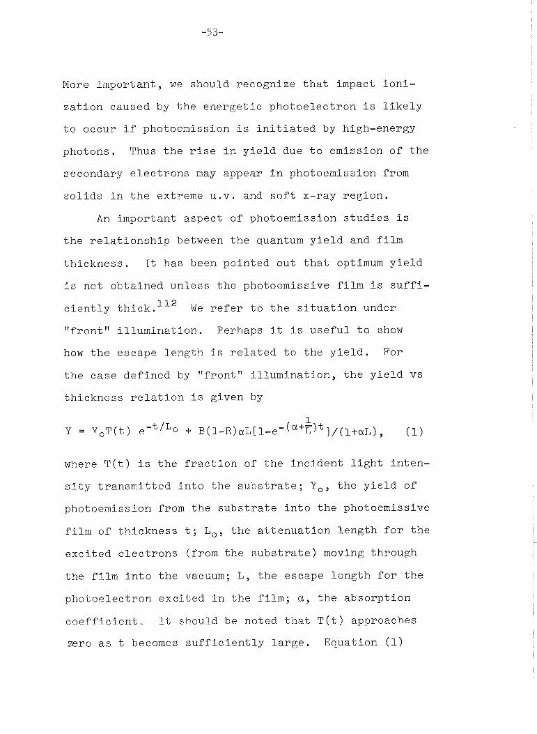
More important, we should recognize that impact ioni-
zation caused by the energetic photoelectron is likely
to occur if photoemission is initiated by high-energy
photons. Thus the rise in yield due to emission of the
secondary electrons may appear in photoemission from
solids in the extreme U.V. and soft x-ray region.
An important aspect of photoemission studies is
the relationship between the quantum yield and film
thickness. It has been pointed out that optimum yield
is not obtained unless the photoemissive film is suffi-
ciently thick. We refer to the situation under
"front" illumination. Perhaps it is useful to show
how the escape length is related to the yield. For
the case defined by "front" illumination, the yield vs
thickness relation is given by
where T(t) is the fraction of the incident light inten-
sity transmitted into the substrate; Yo, the yield of
photoemission from the substrate into the photoemissive
film of thickness t; Lo, the attenuation length for the
excited electrons (from the substrate) moving through
the film into the vacuum; L, the escape length for the
photoelectron excited in the film; a, the absorption
coefficient. It should be noted that T(t) approaches
zero as t becomes sufficiently large. Equation (1)

reduces to
for large values of t. The essential character of
yield vs film thickness data can be explained in terms
of Eq. (1). If the yield saturates rapidly with respect
to thickness, a small escape length compared to the
absorption length is expected.
In order to substantiate the description given by
Eq. (I), we measured the quantum yield of evaporated
KBr films as a function of film thickness in the spec-
tral region between 10 and 23 eV. The yield was meas-
ured immediately after the KBr film was prepared by
vacuum evaporation in situ at approximately 1 x
Torr from a resistance-heated quartz crucible. Each
KBr film was deposited on a polished LiF crystal whose
surface was pre-coated with a thin film of silver 0
(approximately 50% transmission at 1216 A). The silver
film served as a conductive substrate for the insulating
KBr film. The thickness of the KBr film was estimated
from the transmittance data at 10.2 eV. Results of
yield measurements for three different film thicknesses
are shown in Fig. 34. It is interesting to note that 0
the yield does not change appreciably beyond 200 A in
the low yield region. This is illustrated in greater
detail in Fig. 35. However, the optimum yield does not 0
appear unless the thickness is about 900 A in the high-

yield region. An example of this is shown in Fig. 36.
The results are in qualitative agreement with Eq. (1).
7.2 Exciton-Induced Photoemission from KC1 Films
Exciton-induced photoemission is a process in
which the excitons produced by the incident radiation
transfer their energy to F-center electrons, thereby
causing electron emission into the vacuum. Previous
work on exciton-induced photoemission from F-centers
in alkali iodide films was reported some years ago by
Apker and ~aftl'~. The results of their experiments
showed structure in the yield curve at the spectral
region of the exciton band. An attempt to explain
the spectral yield was made by assuming a thin surface
layer in which no exciton-induced emission could arise. 114
However, in later experiments on single crystals of KI,
it was found that an inversion in the exciton-induced
emission yield could be attributed to the sharply peaked
surface reflectivity. 115
Evidence for exciton-induced emission has been
found also in the photoelectric studies of other mate-
rials. In the measurement of photoemission from BaO
containing donor atoms, sharp structure in the spectral
yield curve showed up clearly at 80 OK, and this was
believed to be due to ionization of donor centers by
excitons . In the study of CdS, Shuba 'I7 observed
that the velocity distribution of the emitted photo-
electrons was not sensitive to the change of photon
energy from 5 to 6.5 eV. His results were inter-
preted as an indication of exciton effect. However,
Spicer 'I8 pointed out that a velocity distribution
which is insensitive to photon energy was not suffi-
cient evidence for exciton-induced emission, and the
results could be explained by assuming direct exci-
tation from the defect levels.
The mechanism of exciton-induced emission from
F-centers is still a subject of vigorous discussion.
In the analysis of energy distribution of photo-
electrons from F-centers, Apker et al. explained the
appearance of the low-energy electron emission in
terms of energy loss of the excited electron before
escape. 'I3 Recently, ~~icer''~ suggested that the
velocity distribution observed in their experiment
can also be explained by assuming the exciton relaxes
before giving its energy up to the F-center electron.
While the interpretation of previous measurements
needs to be clarified, there is no doubt that useful
information concerning excitons can be obtained from
experiments on exciton induced photoemission.
KC1 was selected for our experiments because
luminescence and ultraviolet absorption studies on
this material have been reported. 1203121 There is
an exciton band at approximately 8 eV for KC1.

Although photoemission from the valence band of KC1
has been measured,1°9 the electron emission from F-
centers in KC1 films in the presence of exciton
absorption does not appear to have received much
attention. The principal aim of this paper is to
describe some new experimental results on photo-
emission from evaporated KC1 films in the spectral
region of exciton absorption. A gradual rise of
photoelectric emission with time was observed under
steady ultraviolet excitation of approximately 8 eV.
In the presence of strong biasing radiation (visible
light), the gradual enhancement of emission did not
appear. An attempt is made to explain the transient
enhancement in terms of electron emission from new
F-centers formed by excitons.
Experimental Method
Photoelectron emission was measured immediately
after the KC1 film was prepared by vacuum evaporation
in situ at approximately Torr from a resistance-
heated quartz crucible. The KC1 films were deposited
on polished LiF crystals (25 mm diameter and 2 mm
thick) which were pre-coated with a thin film of nickel
or silver. The transmission of the metal film was 0
approximately 60% at wavelength of 1216 A. The pup-
pose of the thin metal film was to provide a cond-uctive

substrate for the KC1 film and to allow sufficient
transmission of radiation for estimating the thick-
ness of the KC1 film. The absorption coefficient of 0 1 a08 KG1 at 1215 A is about 4.2 x lo5 cm- .
The experimental chamber was mounted directly
on the exit-slit housing of a one-meter normal inci-
dence vacuum U.V. monochromator. The chamber was
evacuated continuously with a liquid nitrogen baffled
4-inch diffusion pump. A LN cold trap was also used
near the exit slit of the monochromator. As shown in
Fig. 37, a tungsten foil of known spectral yield was
employed to determine the incident photon flux. Since
the tungsten foil was attached to a linear-motion
feed-through, it was possible to adjust its position
to permit the biasing radiation (visible light) from
a tungsten filament lamp to come through the LiF-
metal film substrate and strike the KC1 film.
Results and Discussion
Figure 38 illustrates the photoelectric yield
of a KC1 film before and after ultraviolet irradia-
tion for 45 minutes in the exciton band. The in-
crease of yield near 8 eV depends on the duration 0
of pre-irradiation at wavelengths of about 1600 A.
There is a noticeable decrease of yield at photon
energies above 9 eV immediately after the irradiation

period at the exciton band. The slight decrease of
yield may be attributed to inelastic collisions of
the photoelectrons from the valence band with the new
defects created by excitons during pre-irradiation.
The enhancement of yield near 8 eV can be interpreted
as exciton-induced photoemission from new F-centers
formed by excitons.
Figure 39 shows the gradual rise of photoemission
currents under steady ultraviolet excitation of wave- 0
length 1577 A for two different excitation intensities.
The rate of enhancement appears to be somewhat greater
for higher excitation intensity. The effect of biasing
radiation (visible light) is illustrated in Fig, 40.
In the presence of exciton absorption, the growth of
emission current appears. If the biasing radiation
is switched on, an abrupt increase of electron emission
current is observed. While the visible light is on,
the current decays rapidly to the level slightly above
the initial emission current. In the presence of the
biasing radiation, the exciton-induced emission current
is quenched.
The photoemission yield of KC1 in the spectral
region between 7.5 and 8.5 eV is probably due to direct
ionization of impurities and to exciton-induced emis-
sion. It is assumed that some initial concentration
of negative-ion vacancies exists in the KC1 film. When
excitons are produced in the film, they may interact

with the vacancies to form F-centers. An F-center
is an electron which has been trapped at a negative
ion vacancy. Assuming that the photoemission yield
is proportional to the F-center concentration, we
may describe the gradual rise in photoemission cur-
rent i as a function of time t in the presence of
exciton absorption by
where K is a constant which depends on the incident
light intensity; F, is the initial concentration of
impurities, and F(t) is the concentration of F-centers
formed by excitons. Thus the gradual rise of photo-
emission may be related to the change of F-center
concentration F(t) . In order to see how the concentration F(t) varies
with time, we must consider the processes which lead
to the generation and decay of F-centers. For sim-
plicity, we write
dF - = AVX - BXF - CF, dt
where V is the vacancy concentration; X, the exciton
concentration; A, a parameter characterizing the
vacancy-exciton interaction; B, a parameter charac-
terizing exciton-F-center interaction; C, a parameter
characterizing direct ionization of the F-centers.
The vacancy concentration V can be written as (Vo - F),

where Vo is the initial vacancy concentration. 122
If the lifetime of the exciton is T , the exciton
concentration X is given by
where I. is the rate at which excitons are produced
per unit volume, and this rate should be proportional
to the incident light intensity. Accordingly, Eq. (2)
becomes
Solving this equation for F = o at t = o, we have
The exponential saturation indicated by Eq. (5) appears
to be in qualitative agreement with experimental obser-
vation. The effect of the biasing radiation can be
understood readily in view of Eq. (5). In the presence
of strong biasing radiation (visible light), the value
of parameter C must be large because the F-centers
created are rapidly ionized by the visible light. Con-
sequently, the ultimate concentration of F-centers is
greatly reduced. Furthermore, this reduced concentra-
tion would be established rapidly in the presence of
strong biasing radiation because the exponent of the
time dependent term increases with C . Hence the gradual
growth of F(t) does not appear.
An attempt was made to check the rate of rise
of the photoemission current for different excita- 0
tion intensities of wavelength 1577 A. Equations (1)
and (5) were used to describe the emission current as
a function of time. As shown in E q . (T), the factor
[(A+B)TI, + C] should be greater for higher light in- tensity. When the intensity was slightly more than
doubled, a factor of about 1.3 times as large was
sufficient to match the experimental data. This sug-
gests that the factor is not a linear function of the
light intensity. A possible explanation for this is
that the dominant term of the expression is (A+B)TI,,
and the lifetime T of the exciton becomes smaller for
larger I. . It should be mentioned that for higher light in-
tensity the gradual growth of emission current with
time does not follow accurately the exponential satu-
ration specified by Eq. (5). The deviation at large
values of time is consistent with the suggestion that
new vacancies can be produced by excitons. 123
Applications
It might be of interest to suggest a possible
application of the exciton-induced effect in KC1
films. Since the production of F-centers by exci-
tons in KC1 occurs only in the spectral region 1500

0 to 1700 A, a photoelectric detector with a KC1-film
photocathode can be used as a spectrally selective 0
device for measuring radiation of approximately 1600 A.
If the device is exposed to the U.V. radiation, the in-
tensity information can be stored in the photocathode.
Upon exposing the photocathode to visible light, the
intensity information will appear as a current pulse.
The pulse height can be related to the U.V. intensity
and exposure time.
7.3 Photoemission from MgF2 Films
Magnesium fluoride has optical properties which
are desirable for vacuum ultraviolet applications.
The transmission quality is almost as good as LiF in
the vacuum U.V. region. The cutoff wavelength is 0
about 1100 A. It is well known that MgF2 is widely
used as a protective coating for mirrors and gratings. 124
A MgF2 layer can preserve the reflecting quality of a
metallized surface by preventing rapid oxidation of
the metal.
The optical properties of MgF2 have been studied
extensively in the vacuum U.V. region.125-127 As shown
in Fig. 41, the absorption curve shows a sharp peak at
11.8 eV. It has been suggested that this peak is due
to an exciton transition, and the absorption beginning
at about 13 eV is due to band-to-band transitions. 127

According to this interpretation, the threshold for
photoemission from the valence band of MgF2 should be
higher than 13 eV.
In order to see whether this conclusion is valid,
we measured the photoemission yield of evaporated MgF2
in the spectral region between 7 and 23 eV. The film
was prepared by evaporating optical-grade MgF2 in situ
at approximately 1 x lom7 Torr from a tantalum boat
onto a polished LiF crystal. The LiF substrate was
pre-coated with a thin film of nickel. The purpose
of the thin nickel film was to provide a conductive
substrate for the MgF2 film. Sufficient transmission 0
at wavelength 1117 A was obtained through the (LiF + Ni)
substrate to estimate the film thickness of MgF2 from
the transmittance data.
The spectral yield was measured for different film
thicknesses. If the film is not sufficiently thick,
the electrons optically excited in the metallized sub-
strate can diffuse through the MgF2 layer and escape
into the vacuum. Figure 42 illustrates this type of 0
photoemission at wavelength of 1608 A for which optical
absorption in MgF2 is very low. A similar effect has
been observed in the photoemission study of A1-A1203
films . l5 The true yield of MgF2 is obtained from meas-
urements on a sufficiently thick layer of the material. 0
The spectral yield of a MgF2 film (approximately 2700 A
thick) is shown in Fig. 43. It is obvious that the

photoelectric threshold is not above 13 eV.
The yield curve shown in Fig. 43 has two notice-
able shoulders which can be related to the optical
properties of MgF2. The rise in yield at 10.3 eV may
be attributed to optical absorption beginning at ap-
proximately 10.3 eV. 126 The additional rise in yield
at 11.2 eV may be associated with a sharp decrease in
reflectance near 11 eV. 127 In Fig. 44, we express
the yield in terms of number of electrons per absorbed
photon by dividing our yield data by (1-R), where R
is the reflectance value reported in reference 27.
The increase in yield at 10.3 eV is clearly shown. 0
If we accept the absorption edge at 1300 A (9.5 eV)
reported by Schneider and OtBryan 128 as the band gap
and the threshold for photoemission from the valence
band as 10.3 eV, we would obtain an electron affinity
of approximately 0.8 eV. According to this model, the
photoemission from MgF2 at photon energies below 10.3 eV
must be interpreted as emission from impurity centers.
This model is not necessarily in disagreement with the
suggestion that the absorption peak at 11.8 eV is asso-
ciated with an exciton transition. As suggested by
Philipp and ~hrenreich''~, exciton states are likely
to be present at energies higher than the band gap in
solids such as MgF2 and alkali halides with relatively
small dielectric constants and large lattice parameters.
The exciton of energy greater than the band gap can

decay by dissociating into a free electron-hole pair.
The electron from this process may escape into the
vacuum.
7.4 Photoemission from KBr-KC1 Mixture.
Optical absorption in mixed system such as KBr-
KC1 has been studied extensively by ~ a h r l ~ ~ . It was
found that a halogen site in the mixture can be occu-
pied either by a C1- or a Br- ion. As a result, two
series of absorption bands were observed. The heights
of the absorption peaks depend on the relative concen-
trations of the two ions. With the exception of the
high energy band of KBr between 8 and 9 eV, the energy
values of the bands generally shift to higher energy
as KBr concentration increases.
In view of the observed change in the absorption
peak with composition, it was considered worthwhile
to measure the photoelectric yield of the mixture KBr-
KC1. From previous work, log we know that the photo-
electric thresholds of KBr and KC1 are approximately
7.8 and 8.7 eV, respectively. The principal aim of
the experiment was to see whether the threshold for
photoemission from the mixture can be shifted by ad-
justing the composition.
A 50-50% mixture of KBr-KC1 was first fused in a
q u a r t z boat. Then the mixture was placed in the expe-
rimental chamber for evaporation and yield measurements.

The experimental chamber with a sealed LiF window
was evacuated continuously by an ion pump. As a
check on the composition, a film of the mixture was
evaporated on a thin LiF substrate, and the optical
density was measured immediately after evaporation.
As shown in Fig, 45, the optical-density data of the
50-50% mixture agree with the results of previous
work12'. Using the same mixture, a film was formed
on a gold-foil substrate for the quantum yield meas-
urements. The spectral yield of the film is shown
in Fig. 46. Comparing the yield of the mixture to
that of pure KBr, we find that there is a significant
difference in yield in the region between 7.8 and 9 eV.
The effective photoemission threshold of the 50-50%
mixture appears to be about 0.4 eV higher than that
of pure KBr. A further study of yield vs composition
would be desirable.

8. PHOTOLUMINESCENCE AND PHOTOCONDUCTIVITY
Although the luminescent properties of molecular
crystals have been studied extensively, the redistri-
bution of the absorbed optical energy and the process
of emission are still not fully understood. For ex-
ample, the fluorescence efficiency of sodium salicylate
is high and uniform over a wide range of the vacuum
U.V. spectrum. Whether the emission is characteristic
of the molecule or the crystal is still a problem for
further study.
In regard to photoconductivity of solids in the
vacuum U.V. region, we must be aware of the photo-
emission effect which can contribute to the measured
response associated with photoconductivity. Because
of the experimental difficulties, it is difficult to
give a reliable interpretation of the photoconductive
response that may appear in this spectral region.
8.1 Temperature Dependence of Photoluminescence of Sodium
Salicylate.
Sodium salicylate is a material which is widely
used as a detector for vacuum ultraviolet radiation.
It has two useful photoluminescent properties. The
peak of the fluorescent intensity lies in the spectral
region in which an ordinary photomultiplier tube (S-11)
has the maximum-response sensitivity. It is particularly

useful in radiation-intensity measurements because
the relative luminescence efficiency of this material
is essentially constant over a wide spectral range in
the vacuum ultraviolet. 21,22
Although sodium salicylate has been used in ra-
diation detection work for many years, only recently
attempts were made to measure its absolute quantum
efficiency. Unfortunately, there appear to be dis-
crepancies in the published results. Kristianpoller 130
reported a quantum efficiency of 64% for incident ra- 0
diation of 2537 A at room temperature. The results
of Allison, Burns, and Tuzzolino 13' indicate a quantum
efficiency of almost 100%. Previous estimate 12' was
only 10%.
An attempt 132 was made to explain the discrepancies
by pointing out that the sensitivity of the phototube
commonly used in the measurements is not independent of
the angle of incidence. If the instrumental problems
are taken into account, the absolute efficiency value
of 99% at room temperature is believed to be the most
reliable one. However, the question concerning the 99%
efficiency arises when the effect of temperature change
is considered. Kristianpoller and Knapp 133 reported
some measurements of fluorescent yield of sodium sali-
cylate at 80 OK. The fluorescence intensity was found
to be 25% higher than that at room temperature. In an
effort to obtain more information on the temperature

effect, we made measurements of the relative lumi-
nescence efficiency at high and low temperatures.
An attempt is also made to provide a theoretical ex-
planation of the temperature dependence.
Dependence on Temperature
When a molecular crystal is excited by incident
radiation, it can dissipate some of its absorbed en-
ergy by internal quenching before making a fluorescent
transition from the lowest excited singlet state. 1 3 4
The excess energy of the excited molecule in a crystal
can be transferred to the crystal lattice inasmuch as
the period of the individual molecular vibration is
much smaller than that of a crystal vibration. Further-
more if the temperature is sufficiently high, the tran-
sition from the lowest excited state to the normal state
may occur without emission of radiation. 1 3 5
For organic molecules, it has been suggested that
the lowest triplet state can account for the temper-
ature dependence of fluorescence and phosphorescence.
If the triplet state intersects the excited singlet
state at a high vibrational level, the quenching of
the fluorescent state becomes more probable with tem-
perature rise. This model assumes that the lowest vi-
brational level of the triplet state is lower than that
of the excited singlet state. It is clear that phos-
phorescence originates from the triplet state because

the low probability of transition from the triplet
state to the normal singlet state implies long-
lived emission.
If we consider a film of sodium salicylate as
a layer of molecular crystals, it may be more con-
venient to describe the fluorescence in terms of
molecular excitons. 137 It is assumed that absorption
of light produces excitons, which may disappear by
luminescence and transformation into heat or triplet
excitons. Thus a relationship between luminescence
and temperature can be established by assuming that
the photoluminescence efficiency is proportional to
the ratio of the number of excitons converted to ra-
diation to the number of excitons formed by the inci-
dent ultraviolet radiation. The ratio138 is given by
where PL is the probability per unit time that the
exciton emits energy in the form of radiation, and
PT is the probability per unit time that the exciton
transfers its energy to lattice vibrations. There is
no reason why PL should be dependent on the temperature.
PT is described by A e where E is the activation
energy of the radiationless transition, and A is a con-
stant which depends on the frequency of lattice vibra-
t i ~ n . ~ ~ ~ If E, is the low temperature luminescence

efficiency, the higher temperature efficiency may be
expressed as
Equation (2) shows that the luminescence efficiency
decreases with increasing temperature.
It may be of interest to see how the activation
energy E can be estimated if experimental data on
relative luminescence efficiency as a function of
temperature are available. If the efficiency at high
temperature is normalized to that at a low reference
temperature To, Eq. (2) can be written as
where s is A/PL. Suppose we select two temperatures
T1 and T2 such that
With these two specified temperature values, we may
eliminate the unknown quantity s and obtain
I I
(yo- Q E / k where R1 = E ~ / E ~ , R2 = E ~ / E ~ ~ and Y = e
The relative luminescence efficiencies at T1 and T2
can be determined by experiment. Hence E can be cal-
culated by solving Eq. (5) for the given values of R1
and R2.

Experimental Method
The monochromatic radiation for the photolumines-
cence experiment was obtained from a 40-cm normal in-
cidence, vacuum monochromator. A windowless hydrogen
discharge tube (Hanovia 906-A32) was used as a light
source. As shown in Fig. 47 a thin LiF window was
placed in front of the exit slit to isolate the sample
chamber from the vacuum chamber of the monochromator.
The purpose of the sealed window was to eliminate the
possible contamination l 4 O of the sodium salicylate
film by diffusion-pump oil vapor and the hydrogen gas
from the light source. The removable parts of the
sample chamber were sealed with copper gaskets. The
stainless steel chamber was evacuated initially by a
sorption pump and then continuously by an ion-pump.
The sodium salicylate film was deposited on a
thin (1 mm) quartz plate by the spray method. The
effects of cooling and heating were studied on the
same sample without breaking the vacuum. The higher
temperature condition was established by placing an
electric heater in the external cavity of the copper
block on which the quartz plate was mounted. The
photoluminescent response was detected by a photomul-
tiplier tube. The current from the photomultiplier
tube was measured by a micro-volt ammeter (Hewlett-
Packard h25A) and a Sanborn-320 recorder. The spectral
0 fluorescent response from 1200 to 1650 A was meas-
ured when a steady-state temperature was observed.
Results and Discussion
The photoluminescent response over the whole
wavelength range decreased with temperature rise.
The average normalized response as a function of
temperature is shown in Fig. 48, The emission in-
tensity at approximately 130 OK is approximately
14% higher than that at room temperature. This is
in satisfactory agreement with the increase of 25%
at 80 OK reported by Kristianpoller and Knapp 133
Our data show that the luminescence intensity de-
creases gradually to about 400 OK. The luminescent
response of the films which were heated to tempera-
0 tures below 400 K appeared to recover upon cooling
in the vacuum. It should be mentioned that if the
sodium salicylate film is heated to temperatures above
450 OK, the luminescence efficiency may be permanently
reduced. Other factors besides temperature quenching
may have to be considered to explain the abrupt de-
crease at the higher temperatures.
The activation energy E for sodium salicylate can
be estimated from the normalized response data shown
in Fig. 48. Since the normalized response represents
the relative luminescence efficiency, the values of
R1 and R2 can be obtained directly from the graph.
From the solution of Eq. ( 5 ) , we find E = 0.07 eV.
A comparison of the relative efficiency described by
Eq. (3) with the experimental data is also shown in
Fig. 48. The relative efficiency curve for s - 3
gives a good fit over a major portion of the data.
The relatively small value of E for sodium sali-
cylate seems to be consistent with the situation in
which the triplet state intersects the excited singlet
state at a vibrational level of energy E above the
minimum energy of the excited singlet state. As the
temperature increases above T o , the fluorescent state
is quenched by the excited singlet-triplet radiation-
less transition. If the minimum energy of the vibra-
tional levels of the triplet state is appreciably
lower than that of the excited singlet state, phos-
phorescence may arise, and it may be more pronounced
for higher temperatures. This is an interesting point
which deserves further theoretical and experimental
investigation.
8.2 Photoconductivity
The search for intrinsic photoconductivity of
alkali-halide crystals in the vacuum ultraviolet has
been discussed by several authors. 1 ~ l - 1 ~ ~ The ex-
perimental problems encountered in their work were

photoemission from the crystal and polarization of
the crystal in the presence of the external electric
field. The recommended technique for reducing pho-
toemission was vacuum evaporation of a LiF film on
the crystal surface. Low light intensities were used
to avoid polarization and the build-up of calor cen-
ters. Although the electrical response to the incident
light was weak (-10 -15 Amp. ) , some workers142 5143 be- lieved they have detected photoconductivity in the
spectral range of the fundamental absorption bands.
The results of the more recent work indicate that the
band-gap energies of some alkali halides can be obtained
from the photoconduction data. 144
Since polarization phenomena contribute a disturb-
ing effect to photoconductivity measurements, we thought
it might be useful to see how the state of polarization
is affected by the photoexcited carriers. A change of
polarization should occur as a result of neutralization
of trapped charges by the optically excited carriers. 145
The method of observation involves the following proce-
dure: 1) Establishment of an internal electric field
by polarization; 2) The rate of decay of the internal
field can be taken as a measure of the rate of excita-
tion of free electrons and holes in the crystal. Thus
the photoresponse should be characteristic of the volume
process. Consequently, the observable effect would be
evidence for photoconductivity in the solid.

We have investigated the photoeffect in the
presence of the internal electric field of a pure
KBr crystal. The dimensions of the crystal were
2 x 12 x 12 mm. Both surfaces (12 x 12 mm) were
coated with gold films for electrical connection
to the electrometer. The crystal was clamped on a
teflon holder in a vacuum chamber. The surface of
2 x 12 mm was exposed to the incident beam of light
from the exit slit of the vacuum U.V. monochromator.
In order to minimize the contribution from photo-
emission, we performed the experiment in the spectral
region near the photoelectric threshold of the crys-
tal. Figure 49 illustrates a typical response at 0
wavelength of 1608 A. In the presence of the exter-
nal electric field, the photoresponse was observed.
The decay of current is an indication of the space-
charge build-up. Upon removing the applied voltage,
i.e., electrode N was grounded, a displacement cur-
rent was observed. When the dark current became suf-
ficiently small, the crystal was exposed to the U.V.
light. A photocurrent appeared. Since the current
was in the direction opposite of that obtained when
the external voltage was applied, the excited carriers
were assumed to be accelerated by the internal elec-
tric field due to the residual space charge.
We have not completed our study of the decay char-
acteristic of polarization as a function of the incident

light intensity. A more detailed investigation would
be desirable.
Another interesting aspect of photoconductivity
study which deserves further attention is the surface
effect due to exciton dissociation. Evidence of this
effect has been presented by Sydor [Phys. Rev. 183,
846 (196911.
EQUIPMENT FOR FURTHER RESEARCH
We recognize that important information on the
photoelectric properties of thin films can be obtained
from the electron-energy-distribution measurements.
For further study, we plan to use a hemispherical ana-
lyzer shown in Fig. 51 to determine the energy distri-
bution of the emitted photoelectrons as a function of
film thickness.

9. CONCLUSIONS
The most significant feature of our work on
secondary standards for intensity measurements is
the experiment in which we showed that the photo-
ionization yield of xenon in the spectral region
of 860 to 1022 8 is unity. The result supports the
suggestion that a rare-gas ion chamber is the most
convenient device to use for absolute intensity 0
measurements below 1000 A. Thus other devices,
including thermocouples, can be calibrated in the 0
800-1000 A region with a xenon ion chamber. The
calibration procedure is simpler than the technique
involving the use of a thermocouple.
In the study of alkali halide films in the 0
spectral region below 1000 A, we found the yields
of some alkali halide films to be almost unity at
photon energies above 2ET, where ET is the photo-
electric threshold of the material. A noticeable
dip in the yield curves was observed at photon en-
ergies of approximately 2E T'
The optimum yield
was not observed unless the photoemissive layer was
sufficiently thick. For example, the optimum yield
of KBr was obtained for a thickness of about 900 8. The explanation for high quantum yield can be
given in terms of low surface barrier and the ratio of
escape length for the photoelectron to the absorption

length for the incident photon. For high yield
materials such as KBr, we have some evidence that
the escape length is slightly longer than the ab-
sorption length.
The most disturbing effect observed in our
photoemission experiments on evaporated metals was
the gradual change of yield with time immediately
after evaporation. This can be attributed to: 1)
contamination of the metal surface by residual gases
in the vacuum system; 2) a gradual change in film
structure immediately after deposition. In spite of
these difficulties, we were able to estimate the
attenuation lengths for the photoelectrons excited
at certain photon energies. The results of our work
can serve as an independent check on the predicted
values of the electron mean free path in metals.
However, we note that a comparison of the theoretical
value of the mean free path with that obtained from
photoemission data is difficult because we have no
reliable information on the initial energy of the
photoelectron. While we have the results suggesting
long attenuation length for the photoelectrons ex-
cited at hV in aluminum, we have no assurance that
the initial energy of the electron is always equal
to energy hv above the Fermi level. If the initial
energy is considerably less than hv, the long atten-
uation length would be in qualitative agreement with
the theory.

In our study of semiconducting crystals, we
suggested that the difference in yields of n and
p-type Sic is an indication of band bending at the
surface of the crystal. Our experimental results
are in agreement with the conclusion that the p-
type crystal of semiconductors has the higher yield.
According to our results on photoemission from
Si crystals, the yield due to photoemission from the
silicon oxide layer appears to be quite significant 0
in the spectral region below 1100 A. In order to
see if this conclusion is correct, attempts are being
made to determine the quantum yield of pure silicon
monoxide.
The spectral-yield curve of MgF2 indicates a
noticeable rise in yield at photon energies asso-
ciated with an exciton transition. The result is
best explained by assuming the presence of exciton
states at energies higher than the band gap of MgF2.
In this study, we also pointed out that the true
yield of evaporated MgF2 is not obtained unless the
film is sufficiently thick. We demonstrated how the 0
photoemission yield at wavelength of 1608 A decreased
with increasing MgF2 thickness. The photoemission
was due to photoelectrons excited in the metallic sub-
strate. Since these electrons must diffuse through
the MgF2 layer in order to escape into the vacuum, the
emission can be attenuated by increasing thickness of

MgP2. This situation suggests a method by which one
can determine experimentally how low-energy electrons
can be attenuated in a medium which has low photo-
electric yield. For example, films of organic mate-
rials can be evaporated on the metallized substrate
to attenuate the emission of photoelectrons. From
the analysis of the data, we should be able to deter-
mine the electron mean free path in the material.l5
Evidence of exciton-induced photoemission was
found in our study of photoemission from evaporated
KC1 films. The exciton effect appeared as a gradual
enhancement of photoemission with time under steady
U.V. excitation in the exciton band. The transient
-effect was attributed to the creation of new F-centers
by excitons. The fact that the gradual rise is not
observed in the presence of strong biasing radiation
(visible light) indicates that the F-centers can be
ionized rapidly by the visible light and hence the
rate of exciton-F center interaction can be greatly
reduced.

10. REFERENCES
L. Dunkelmann, J. Quant. Spectrosc. Radiat. Transfer.
2 , 533 (1962).
L . Dunkelman, J.P. Hennes, and W.B. Fowler, Space
Research 111, p. 1174, W. Priester, ed., North-
Holland Publishing Company, Amsterdam (1963).
E. Taft and H.R. Phillip, J. Phys. Chem. Solids 1,
159 (1956); 3, 1 (1957).
A.H. Sommer, "Photoemissive Materialstt, pp. 186-
221, John Wiley and Sons, Inc., New York (1968).
D.M. Packer and C. Lock, J. Opt. Soc. Am. 41,
699 (1951).
H.E. Hintereger, J. Quant. Spectrosc. Radiat.
Transfer. 2, 561 (1962).
F.M. Matsunaga, R.S. Jackson, and K. Watanabe,
J. Quant. Spectrosc. Radiat. Transfer 5, 329 (1965).
K. Watanabe, F.M. Matsunaga, and H. Sakai, Appl.
optics 6, 391 (1967).
P.H. Metzger, J. Phys. Chem. Solids 26, 1879 (1965).
W. Pong and R. Norris, J. Opt. Soc. Am. 55, 1189
(1965).
W. Pong and K. Fujita, J. Appl. Phys. 37, 445 (1966).
W. Pong, R. Sumida, and G. Moore, J. Appl. Phys.
41, 1869 (1970).
13. W. Pong, J. Appl. Phys. 37, 3033 (1966).
14. w. Pong, J. Appi.. Phys. 38, 4103 (1967).

W. Pong, J. ~ p p l . Phys, 40, 1733 (1969).
K. Watanabe and E.C.Y. Inn, J. Opt. Soc. Am. 43,
32 (1953); N. Wainfan, W.C. Walker, and G.L. Weissler,
J. Appl. Phys. 24, 1318 (1953).
NBS standard lamp C-980.
R.G. Johnston and R.P. Madden, Appl. Optics 4,
1574 (1965).
K. Watanabe, F.M. Matsunaga, and R.S. Jackson
"Some Intensity Measurements in the Vacuum Ultra-
violet" (June, 1964) NASA-Report.
Measured at NBS according to procedure described
in ref. 18.
J.A.R. Samson, J. Opt. Soc. Am. 54, 6 (1964).
K. Watanabe and C.Y. Inn, J. Opt. Soc. Am. 43,
32 (1953).
H.Y. Fan, Phys. Rev. 68, 43 (1945).
M.J. Buckingham, Phys. Rev. 80, 704 (1950).
F. Wooten and T. Huen, J. Opt. Soc. Am. 57, 102
(1967) *
F.J. Piepenbring - "Optical Properties and Elec-
tronic Structure of Metals and Alloys" (North-
Holland Publishing Co., Amsterdam, 1966) pp. 316-323.
L. Sutton, Phys. Rev. Letters 24, 386 (1970).
N.V. Smith and W.E. Spicer, Phys. Rev. 188, 593
(1969).
E.O. Kane, Phys. Rev, 147, 335 (1966).
W.E. Spicer, J. Appl. Phys. 31, 2077 (1960).

A . J , Dekker , S t o l i d S t a t e P h y s i c s , e d i t e d by
F. S e i t z and D . T u r n b u l l , V o l . 6 , Academic P r e s s ,
I n c . , New York, 1958, p . 251.
E . O . Kane, J . Phys . Soc . of J a p a n 21, Supplement
P O 37 ( 1 9 6 6 ) .
E . Merzbacher , "Quantum Mechanics" p . 470, J o h n
Wiley & Sons, I n c . ( 1 9 6 1 ) .
C . N . Berg lund and W.E. S p i c e r , Phys . Rev. 136 ,
A 1030 ( 1 9 6 4 ) .
K . Mot i zuk i and M . S p a r k s , J . Phys . Soc . o f J a p a n
1 9 , 486 ( 1 9 6 4 ) .
J . J . Quinn , Phys . Rev. 126 , 1453 ( 1 9 6 2 ) .
J . J . Quinn , Appl . Phys . L e t t e r s 2 , 1 6 7 ( 1 9 6 3 ) .
S .L . Ad le r , Phys. Rev. 130 , 1654 ( 1 9 6 3 ) .
R . H . R i t c h i e and J . C . Ashley , J . Phys . Chem.
S o l i d s 26, 1689 ( 1 9 6 5 ) .
S . Raimes, R e p t s . P r o g r . Phys . 20, 1 ( 1 9 5 7 ) .
R.W. Davies , Phys. Rev. 181 , 11-18 ( 1 9 6 9 ) .
C . R . Crowel l , W . G . S p i t z e r , L.E. Howarth, and
E . E . LaBate, Phys. Rev. 127 , 2006 ( 1 9 6 2 ) .
C . R . Crowel l and S.M. S z e , " P h y s i c s o f Th in F i lms"
v o l . 4 , pp . 325-371 ( 1 9 6 7 ) , Academic P r e s s , New York.
G . A . K a t r i c h and O . G . S a r b e i , S o v i e t Phys . -So l id
s t a t e 3 , 1 1 8 1 ( 1 9 6 1 ) .
S.M. S z e , J . L . Mol l , and T. Sugano, S o l i d - S t a t e
E l e c t r o n i c s 7 , 509 ( 1 9 6 4 ) .
R . S t u a r t , F . Wooten, W.E. S p i c e r , Phys . Rev. 135 ,
A 4 9 5 ( 1 9 6 4 ) .

L. R. Canfield, G. Hass, and W. R. Hunter, Le
Journal De Physique 25, 124 (1964).
L.R. Canfield, G. Hass, and J. E. Waylonis,
~ppl. Optics 5, 45 (1966)-
W.R. Hunter, Le Journal De Physique 25, 154 (1964).
R.P. Madden, L.R. Canfield, and G. Hass, J. Opt,
Soc. Am. 53, 620 (1963).
B.P. Feuerbacher and W. Steinmann, Optics Commu-
nications 1, 81 (1969).
R.N. Stuart and F. Wooten, Phys. Rev. 156, 364
(1967) *
H. Kanter, Phys. Rev. B, 1, 522 (1970).
A.J. Blodgett, Jr. and W.E. Spicer, Phys. Rev.
146, 390 (1966).
J.R. Cuthill, A.J. McAlister, M.L. Williams, and
R.E. Watson, Phys. Rev. 164, 1006 (1967).
H.D. Hagstrum and G.E. Becker, Phys. Rev. 159,
572 (1967).
D.E. Eastman and W.F. Krolikowski, Phys. Rev.
Letters 21, 623 (1968); D.E. Eastman, J. Appl.
Phys. 40, 1387 (1969).
R.C. Vehse and E.T. Arakawa, Phys. Rev. 180,
695 (1969) *
J. Toots, H.A. Fowler, and L. Marton, Phys.
Rev. 172, 670 (1968).
P.A. Wolff, Phys. Rev. 95, 56 (1954).
F. Wooten and R.N. Stuart, Phys. Rev. 186, 592
(1969).

W.E. Spicer, J. Phys. Chem. Solids 22, 365 (1961).
E.O. Kane, Phys. Rev. 159, 624 (1967).
P.A. Wolff, Phys. 95, 1415 (1954).
F. Seitz, Phys. Rev. 76, 1376 (1949).
J. Appel, Phys. Rev. 125, 1815 (1962).
A.H. Sommer and W.E. Spicer, "Photoelectric Materials
and Devices", Edited by S. Larach, D. Van Nostrand
Co., Inc., New York, 1965, p. 181.
E.O. Kane, Phys. Rev. 127, 131 (1962).
D. Redfield, Phys. Rev. 124, 1809 (1961).
N.B. Kindig, J. Appl. Phys. 38, 3285 (1967).
H.R. Philipp and E.A. Taft, Phys. Rev. 120, 37
(1960) *
T. Sasaki and K. Ishiguro, Phys. Rev. 127, 1091
(1962).
W.E. Spicer and R.E. Simon, Phys. Rev. Letters 9,
385 (1962).
W.E. Spicer and R.E. Simon, J. Phys. Chem. Solids
23, 1817 (1962).
G.W. Gobeli and F.G. Allen, Phys. Rev. 127, 150
(1962).
T.A. Callcott, Phys. Rev. 161, 746 (1967).
L. Patrick, D.R. Hamilton, W.J. Choyke, Phys. Rev.
143, 526 (1966).
R.N. Ghoshtagore and R.L. Coble, Phys. Rev. 143,
623 (1966).

H.R. Philipp and E.A. Taft, Proc. Conf. Silicon
Carbide, J.R. O1Connor and J. Smiltens (Eds.),
Pergamon, New York, 1960.
B.C. Deaton and F.A. Blum, Jr., Phys. Rev. 137,
A1131 (1965).
R. Kaplow, T.A. Rowe, and B.L. Averbach, Phys.
Rev. 168, 1068 (1968).
M.P. Givens, Rev. Sci. Instr. 25, 1130 (1974).
A. von Hippel, J. Chem. Phys. 16, 372 (1948).
H. Merdy, S. Robin-Kandare, and J. Robin, C.R.
Acad. Sci. (France) 257, 1526 (1963).
A.G. Leiga, J. Opt. Soc. Am. 58, 1441 (1968).
J.D. Hayes, E.T. Arakawa, and M.W. Williams,
J. Appl. Phys. 39, 5527 (1968).
D. Pines, Rev. Mod. Phys. 28, 184 (1956).
M. Cardona, Phys. Rev. 129, 69 (1963).
T. Goto, T. Yashiro, and M. Ueta, J. Phys. Soc.
Japan 20, 2185 (1965).
J. Mattler, Compt. rend. 217, 447 (1943).
D.W. Turner, Nature 179, 1022 (1957).
A.H. Sommer, RCA Rev. 28, 75 (1967).
M. Rome, IEEE Transactions on Nuclear Science,
pp. 93-99, June, 1964.
W.F. Krolikowski and W.E. Spicer, Bull. Amer.
Phys. Soc. 9, 735 (1964); Technical Report
No. 5218-1, May 1967.
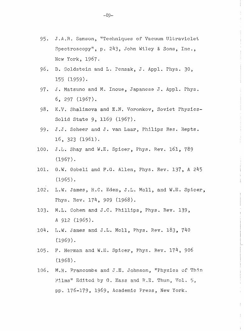
95. J.A.R. Samson, "Techniques of Vacuum Ultraviolet
SpectroscopyTt, p. 243, John Wiley & Sons, Inc.,
New York, 1967.
96. B. Goldstein and L. Pensak, J. Appl. Phys. 30,
155 (1959).
97. J. Matsuno and M. Inoue, Japanese J. Appl. Phys.
6, 297 (1967).
98. K.V. Shalimova and E.N. Voronkov, Soviet Physics-
Solid State 9, 1169 (1967).
99. J.J. Scheer and J. van Laar, Philips Res. Repts.
16, 323 (1961).
100. J.L. Shay and W.E. Spicer, Phys. Rev. 161, 789
(1967)
101. G.W. Gobeli and F.G. Allen, Phys. Rev. 137, A 245
(1965)
102. L.W. James, R.C. Eden, J.L. Moll, and W.E. Spicer,
Phys. Rev. 174, 909 (1968).
103. M.L. Cohen and J.C. Phillips, Phys. Rev. 139,
A 912 (1965).
104. L.W. James and J.L. Moll, Phys. Rev. 183, 740
(1969)
105. F. Herman and W.E. Spicer, Phys. Rev. 174, 906
(1968).
106. M.H. Francombe and J.E. Johnson, "Physics of Thin
Films" Edited by G. Hass and R.E, Thun, Vol. 5,
pp. 176-179, 1969, Academic Press, New York.

J . L . R i c h a r d s , P.B. Hart, and L.M. Ga l lone ,
J . Appl. Phys . 34, 3418 ( 1 9 6 3 ) .
H . R . P h i l i p p and H . E h r e n r e i c h , Phys . Rev. 131 ,
2016 ( 1 9 6 3 ) .
E.A, T a f t and H . R . P h i l i p p , J . Phys . Chem.
S o l i d s 3, 1 ( 1 9 5 7 ) .
J .E . Eby, K . J . Teegarden , and D . B . D u t t o n , Phys.
Rev. 116 , 1099 ( 1 9 5 9 ) .
S.W. Ducke t t and P.H. Metzger , Phys . Rev. 137 ,
A 953 ( 1 9 6 5 ) .
L. Heroux, W . J . McMahon, and H.E. H i n t e r e g g e r ,
~ p p l . O p t i c s 5 , 1338 ( 1 9 6 6 ) .
L. Apker and E. T a f t , Phys . 79, 964 ( 1 9 5 0 ) ;
Phys . Rev. 81 , 698 (1951) ; Phys . Rev. 82 , 814
(1951) *
M . H . Hebb, Phys . Rev. 81 , 702 ( 1 9 5 1 ) .
H . R . P h i l i p p and E.A. T a f t , Phys. Rev. 1 0 6 , 671
(1957)
E.A. T a f t , H . P h i l i p p , and L. Apker, Phys. Rev.
113, 156 (1959) .
J . A . Shuba, S o v i e t Phys. Tech. Phys. 1, 1104
( 1 9 5 6 ) .
W.E. S p i c e r , J . Phys . Chem. S o l i d s 20, 134
(1961) *
W.E. S p i c e r , Phys . Rev. 1 5 4 , 385 ( 1 9 6 7 ) .
P.L. Hartman, J . R . Nelson , and J . G . S i e g r i e d ,
Phys. Rev. 105 , 123 ( 1 9 5 7 ) .

T. Timusk and W. Martienssen, Phys. Rev. 128,
1656 (1962).
J.H. Parker, Jr., Phys. Rev. 124, 703 (1961).
P.V. Mitchell, D.A. Wiegand, and R. Smoluchowski,
Phys. Rev. 121, 484 (1961).
G. Hass and R. Tousey, J. Opt. Soc. Am. 49,
593 (1959).
A. Duncanson and R.W.H. Stevenson, Proc. Phys.
Soc. London 72, 1001 (1958).
B. Vodar, J. Quant. Spectry. and Radiative
Transfer 2, 393 (1962).
M.W. Williams, R.A. MacRae, and E.T. Arakawa,
J. Appl. Phys. 38, 1701 (1967).
E.G. Schneider and H.M. OtBryan, Phys. Rev. 51,
293 (1937).
H. Mahr, Phys. Rev. 122, 1464 (1961).
N. Kristianpoller, J. Opt. Soc. Am. 54, 1285
(1964)
R. Allison, J. Burns, and A.J. Tuzzolino, J.
Opt.. Soc. Am. 54, 747 (1964).
K.J. Nygaard, J. Opt. Soc. Am. 55, 944 (1965).
N. Kristianpoller and R.A. Knapp, Appl. Optics
3, 915 (1964).
F.D. Brooks, "Progress in Nuclear ~hysics",
Vol. 5, edited by O.R. Frisch (Pergamon Press,
London and New York, 1956)~ p. 252.
N.F. Mott, Proc. Roy. Soc. (A), 167, 384 (1938).

M. Kasha, Chem. Revs. 41, 401 (1947).
R.M. Hochstrasser, Revs. Mod. Phys. 34, 531 (1963).
A.S. Davydov, "Theory of Molecular Excitons",
translated by M. Kasha and M. Oppenheimer, Jr.
(McGraw-Hill Book Co,, Inc., New York, 1962). p. 117.
F.A. Kroger, "Some Aspects of the Luminescence of
Solids" (Elsevier Publishing Co., Inc., New York,
1948), p. 213.
R.A. Knapp and A.M. Smith, Appl. Optics 3, 637 (1964).
J.W. Taylor and P.L. Hartman, Phys. Rev. 113, 1421
(1959) *
Y. Nakai and K. Teegarden, J. Phys. Chem. Solids
22, 327 (1961).
G. Kuwabara and K. Aoyagi, J. Phys. Chem. Solids
22, 333 (1961).
G.R. Huggett and K. Teegarden, Phys. Rev. 141,
797 (1966)
J.A. Elmgren and D.E. Hudson, Phys. Rev. 128,
1044 (1962).

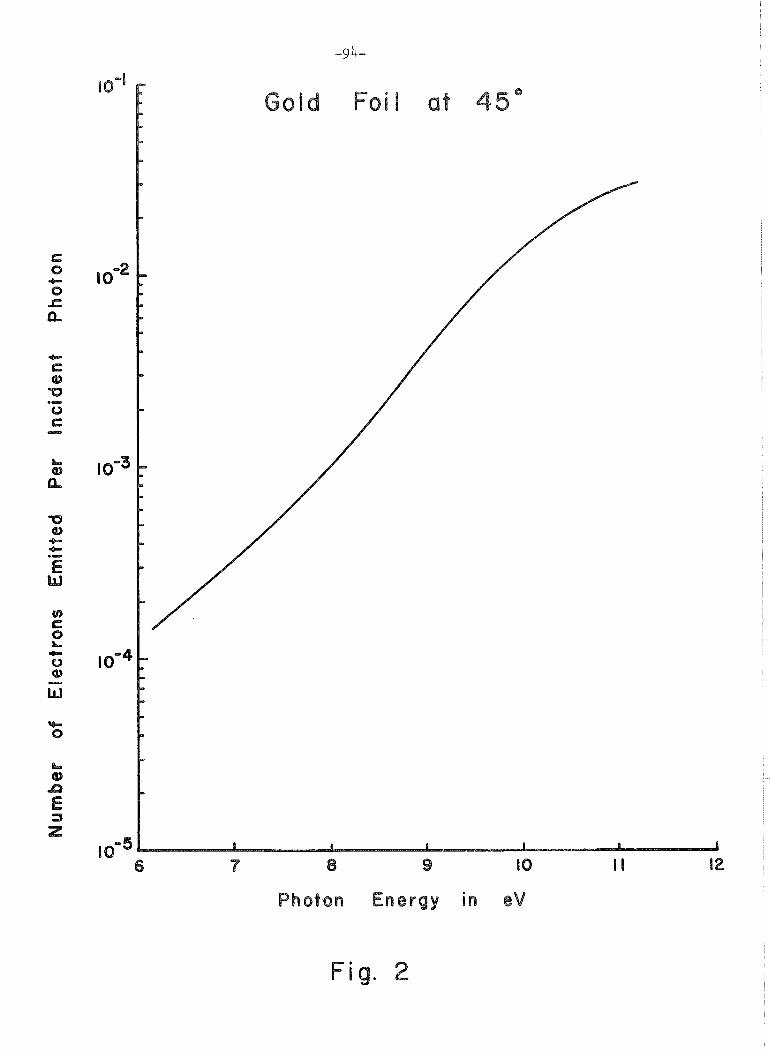
-94-
Gold Foi at 45"
Photon Energy in eV
Fig. 2


"3QCUUrn /Electron is optically
excited,
surface
I Electron is optically
vacuum excited.
I
surface
Electron is optically x excited.
vacuum
I
S I surface i
Fig. 4

-97-
Fig . 5 a " ~ r o n t " i l l u m i n a t i o n
Vacuum f i l m
e l e c t r o n
s u b s t r a t e ( L iF crysta l 1
Fig. 5 b " ~ a c k " i l l umina t ion
ec t ron

uv l i g h t
I I vacuum uv
monochroma tor
l i n e a r motion f e e d through
e lec t romstsr
e lec t rometer
Photoemission Chamber
Fig. 6 Top-view of experimental chamber for measuring photoemission from evaporated films under "back" illumination.
(I] (I]
2 5 .rl
5
E v a g . G s l d
P h o t o n E n e r g y i n e V
Fig. 9 Photoemission from gold films under "back" illumination.

Photon E n e r g y in eV
Fig. 10 Photoemission from aluminum films under "back" illumination.
Evap. A l
hv = 10.2 eV
Fi lm T h i c k n e s s in
0
Fig. 11 o Experimental data ; Calculated curve for L= 238 A.

Evap. A1
Evap. Gold
Photon E n e r g y i n e V
Fig. 12 Attenuation length values for photoelectrons in aluminum and gold films.


Photon Energy in eV
Fig. 14 Photoemission from nickel films under "back" illumination. The films were evaporated on LiF substrates.

Linear- motion
cold trap
Monochroma tor
D i f f us ioa pump
~ig.16 Equipment for Photoemission Measurements
at Photon Energies be tween 10 and 23 cV


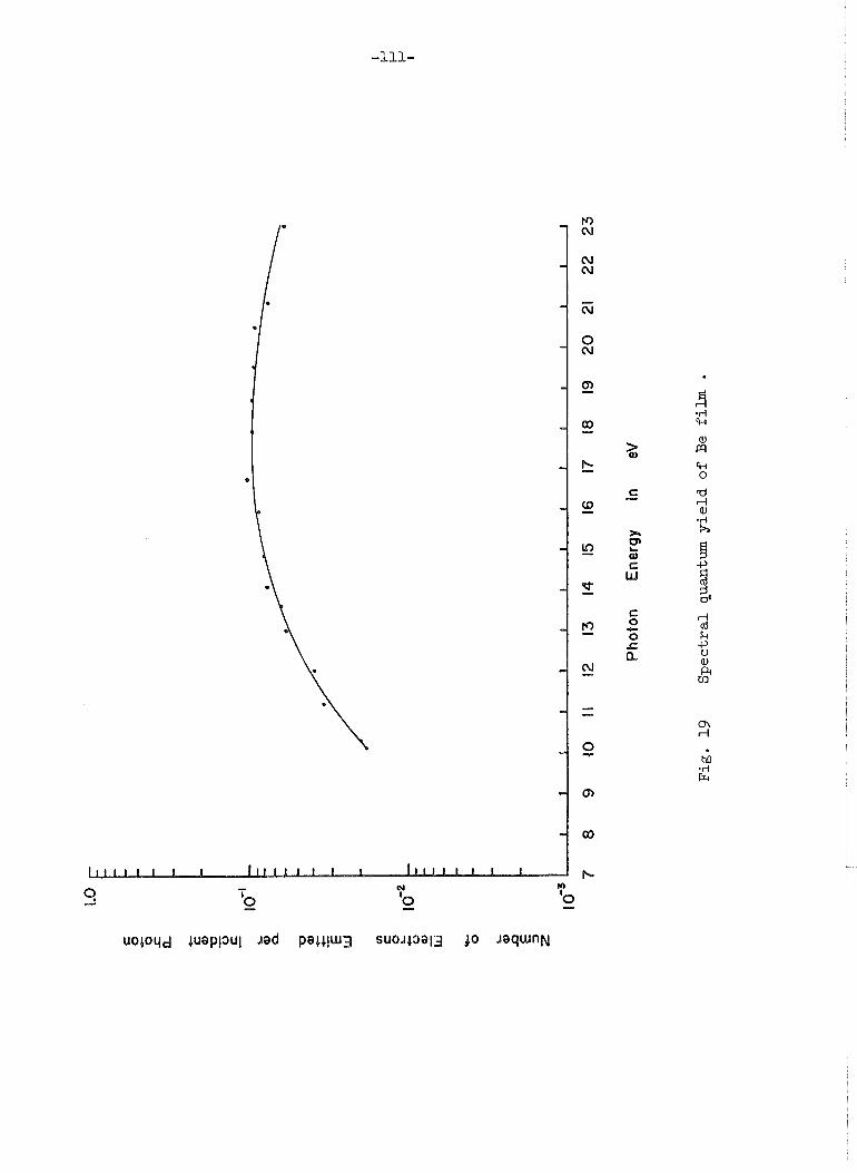

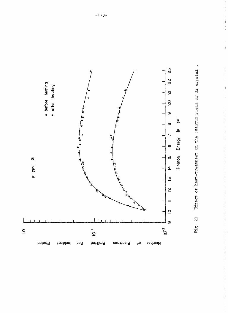
Number of Electrons Emitted Per Incident Photon

Pho
ton
Ene
rgy
in
eV
Fig
. 2
2
Sp
ec
tra
lqu
an
tum
yie
ldo
fh
ea
t-tr
ea
ted
sic
ry
sta
l.

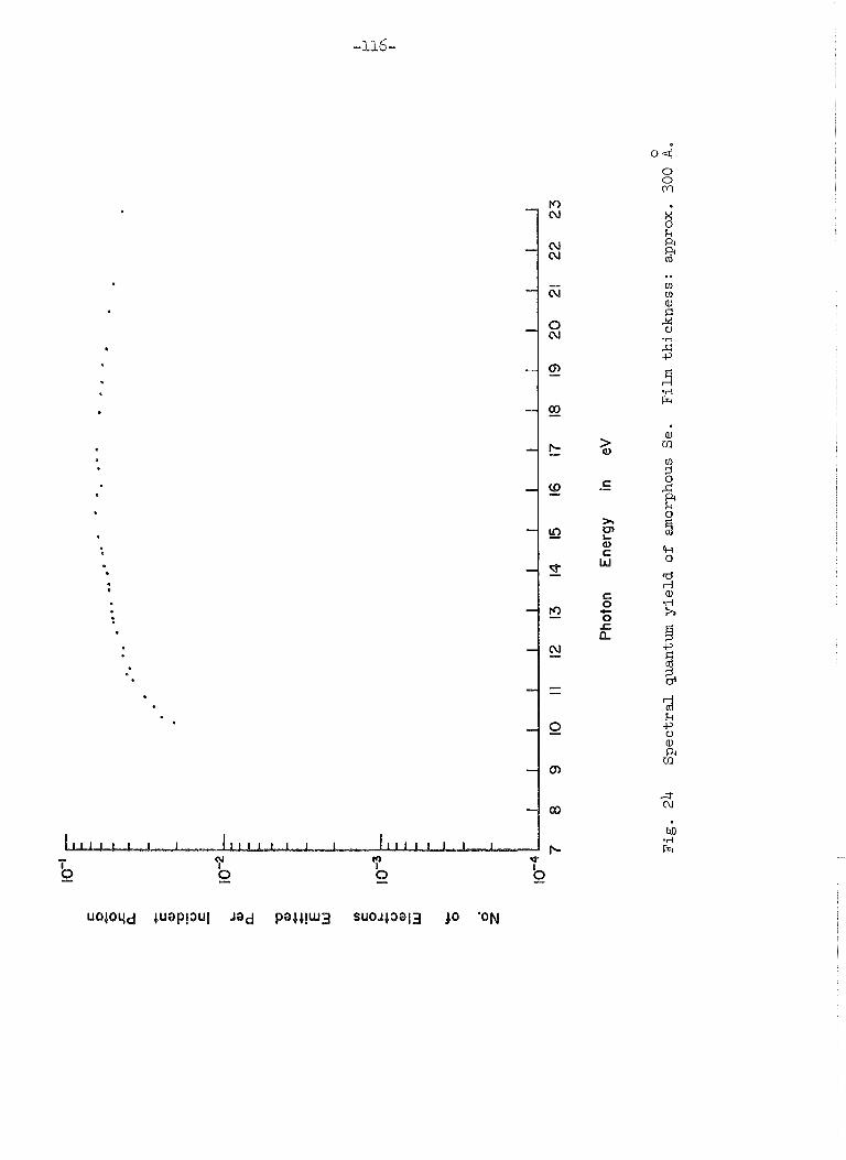


tJl td (D n d- Y P I-'
ct- (D t-' I-'
6 i

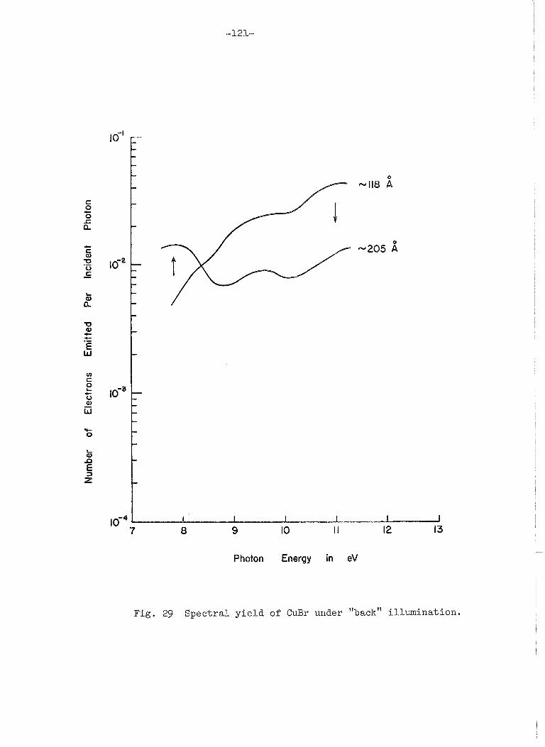
Photon Energy in eV
Fig. 29 S p e c t r a l y i e l d of CuBr under "back" i l l u m i n a t i o n .


. .
. .
.
. . .
4 .
4 - - uo+oyd +uap!aul l a d pa$+!luI suoJ+aalg 40 JaqlunN


Linear-motion Feedthrough
Cold Trap
Monochromator
Fig. 37 Exciton-induced photoemission experiment.


Fig. 39 Exciton-hnduced photoemission from KC1 film at 1577 A. Excitation intensity (1577 8) of A was approximately twice that of B .


Pho
ton
Ene
rgy
in eV
Fig. 44
Spectral yield of MgF2 film: corrected for reflectivity. The yield
is expressed in number of electrons per absorbed photon.


Photon Energy in eV
Fig. 46 Spectral yield of 50-50% KBr-KC1 film.

vacuum UV monochrom~tor
Fig. 47 Equipment for measuring the fluorescence of sodium s ali cylat e .

0 m Ic 0 q m N - ? e * 6 0 d 8 d o d d d 0


0 0 w
2 9
!?i g .- - O
i 2
(U - (duo ,,-0l) +uaJln3 uolss!luao+oqd

Fig. 51 Hemispherical analyzer for electron energy distribution measurements. S is the LiF subs- trate for the film; H, hemispherical analyzer; C, electron collector.

EQUIPMENT for PHOTOEMISSION
EXPERIMENTS INVOLVING "BACK"
ILLUMINATION ABOVE l I00 a .

EQUIPMENT for PHOTOEM ISSION
EXPERIMENTS in the SPECTRAL
REGION 10 to 23 eV.

E Q U I P M E N T for PHOTOLUMINESCENCE
STUDY of SODIUM SALICYLATE a t
DIFFERENT TEMPERATURES.
- 146-