Embed Size (px)
Citation preview
Surface photovoltage phenomena:theory, experiment, and applications
Leeor Kronik,* Yoram Shapira
Department of Physical Electronics, Tel-Aviv University, Ramat-Aviv 69978, Israel
Amsterdam±Lausanne±New York±Oxford±Shannon±Tokyo

Contents
1. Introduction 5
2. General theory 7
2.1. Electrical properties of semiconductor surfaces 7
2.1.1. Fundamental concepts 7
2.1.2. Gap states 9
2.1.3. Surface space charge region 13
2.1.4. Surface dipoles 16
2.1.5. Interface space charge regions 19
2.2. Surface photovoltage (SPV) 24
2.2.1. Basic concepts 24
2.2.2. Super-bandgap SPV 25
2.2.3. Sub-bandgap SPV 38
2.2.4. The Dember potential 45
2.2.5. Effect of buried interfaces 47
3. Experimental methods 49
3.1. The Kelvin probe 49
3.1.1. Principles of operation 49
3.1.2. Practical considerations 51
3.1.3. Limitations and solutions 57
3.1.4. Scanning Kelvin probes 61
3.2. MIS structures 64
3.3. Other methods 68
3.3.1. E-beam analysis 68
3.3.2. Photoelectron spectroscopy 71
3.4. High resolution scanning techniques 73
3.4.1. Kelvin probe force microscopy 73
3.4.2. Scanning tunneling microscopy 79
4. Basic surface photovoltage spectroscopy 84
4.1. Bandgap energy and semiconductor type 85
4.2. Gap state spectroscopy 92
4.3. Points of importance 106
5. Advanced analyses 111
5.1. Carrier diffusion length 111
5.1.1. Analysis principles 111
5.1.2. Practical considerations 116
5.1.3. Limitations and solutions 119
5.2. Surface band bending and dipole 128
5.2.1. Surface band bending ± photosaturation 128
5.2.2. Surface band bending ± other methods 138
5.2.3. Surface dipole 143
5.3. Recombination rates 148
5.4. Surface states 153
5.4.1. Energy distribution 153
5.4.2. Properties 160
5.4.3. Distinction between surface and bulk states 168
2 L. Kronik, Y. Shapira / Surface Science Reports 37 (1999) 1±206

5.5. Thin ®lms and heterstructures 170
5.5.1. Spectroscopy of multilayer structures 171
5.5.2. Spectroscopy of quantum structures 179
5.5.3. Construction of band diagrams 183
6. Concluding remarks 188
Acknowledgements 189
References 189
L. Kronik, Y. Shapira / Surface Science Reports 37 (1999) 1±206 3

Surface Science Reports 37 (1999) 1±206
Surface photovoltage phenomena: theory, experiment,and applications
Leeor Kronik,* Yoram Shapira
Department of Physical Electronics, Tel-Aviv University, Ramat-Aviv 69978, Israel
Manuscript received in ®nal form 18 May 1999
Abstract
The theoretical concepts, experimental tools, and applications of surface photovoltage (SPV) techniques are reviewed in
detail. The theoretical discussion is divided into two sections. The ®rst reviews the electrical properties of semiconductor
surfaces and the second discusses SPV phenomena. Next, the most common tools for SPV measurements and their relative
advantages and disadvantages are reviewed. These include the Kelvin probe and the use of MIS structures, as well as other less
used techniques. Recent novel high-spatial-resolution SPV measurement techniques are also presented. Applications include
surface photovoltage spectroscopy (SPS) which is a very effective tool for gap state spectroscopy. An in-depth review of
quantitative analyses, which permit the extraction of various important surface and bulk parameters, follows. These analyses
include: carrier diffusion length; surface band bending, charge, and dipole; surface and bulk recombination rates; surface state
distribution and properties; distinction between surface and bulk states; spectroscopy of thin ®lms, heterostructures and
quantum structures; and construction of band diagrams. Finally, concluding remarks are given. # 1999 Elsevier Science B.V.
All rights reserved.
1. Introduction
The surface photovoltage (SPV) method is a well-established contactless technique for thecharacterization of semiconductors, which relies on analyzing illumination-induced changes in thesurface voltage. For ®ve decades, it has been used as an extensive source of surface and bulkinformation on various semiconductors and semiconductor interfaces. During that time, the SPVtechnique has continuously evolved: newer, better and more diverse experimental tools have emerged.Simultaneously, more sophisticated methods and algorithms for data analysis have also appeared.
0167-5729/99/$ ± see front matter # 1999 Elsevier Science B.V. All rights reserved.
PII: S0167-5729(99)00002-3
ÐÐÐÐ* Corresponding author. Present address: Department of Chemical Engineering and Materials Science, University of
Minnesota, Minneapolis, MN 55455, USA. Fax: +1-612-626-7246
E-mail address: [email protected]
Studies of the effects of illumination on the surface voltage had begun in the late 1940s and early1950s with the classical articles of Nobel prize laureates Brattain and Bardeen [1±3]. Consequently,Johnson has shown that surface photovoltage measurements may yield minority carrier lifetimes [4]and Goodman has developed an algorithm for easy extraction of the minority carrier diffusion length[5]. The next major breakthrough in SPV methods took place in the early 1970s, when systematicresearch on the effects of sub-bandgap illumination on the surface voltage took place by Gatos et al. [6].These researchers realized that they had invented a powerful tool for surface state characterization andalso coined the term `surface photovoltage spectroscopy' (SPS).
Brillson used SPS extensively throughout much of the 1970s and 1980s to study a great variety ofsemiconductor surfaces [7]. In many of his works, he has shown that the simultaneous use of SPS with`main stream' analytical surface techniques makes it possible to obtain an unequivocal correlationbetween the chemical/structural and electronic properties of the surface. MoÈnch, Heiland, and LuÈthwere also among the ®rst outside Gatos' group to realize the potential of SPS and have utilized it forstudying Ge, Si, GaAs, and ZnO [8±10]. Speci®cally, MoÈnch has been an active user and developer ofwork function techniques in general, and SPV methods in particular [11].
The 1990s have seen a renewed vigor in the development of SPV related techniques. Lagowski et al.have scanned the SPV across an entire Si wafer, relating areas of different voltage to areas of heavymetal contamination or to surface defects [12]. Several groups have applied scanning tunnelingmicroscopy (STM) [13,14] and atomic force microscopy (AFM) [15] tips for obtaining SPVmeasurements with a greatly improved lateral resolution. The importance of the surface photovoltaiceffect in photoemission measurements has been pointed out [16±18], leading to both a renewed interestin SPV and an extensive re-examination of the interpretation of many previous photoemissionexperiments. Finally, the authors of this treatise have systematically applied SPV methods for thequantitative study of buried interfaces at semiconductor heterojunctions [19±21].
Despite the great body of work, of which only the `tip of the iceberg' has been mentioned in thepreceding discussion, no single treatise devoted solely to an in-depth description of the SPV techniquehas appeared. The present manuscript is intended to provide a tutorial review of both theory andapplications of SPV methods in general, and SPS in particular. We have tried to cover all aspects of thetechnique, from the earliest theoretical and experimental achievements to the latest developments.
Following this brief introduction of the SPV technique and its uses, the second chapter is devoted to astructured presentation of the physical and mathematical groundwork necessary for a comprehensiveunderstanding of the method. The chapter is divided into two sections. The ®rst reviews the electricalproperties of semiconductor surfaces, including gap states, surface dipoles and the surface space chargeregion (SCR). These concepts are immediately put to use in the following section, devoted to principlesof the surface photovoltaic effect.
The third section of the review is devoted to a survey of the experimental methods available forcarrying out SPV experiments. It begins with a detailed discussion of the two most important SPVmeasurement methods, namely, the Kelvin probe and the capacitive pick-up technique. Othertechniques are then reviewed, including high lateral resolution STM- and AFM-based approaches.
Having laid down both the theoretical and experimental groundwork of the SPV technique, the fourthchapter deals with fundamentals of SPS experiments. It describes the most basic analyses of SPVspectra, namely, the determination of semiconductor type (p or n) and bandgap energy, and theidenti®cation of gap states. Various applications of the basic analysis are reviewed. A special section isdevoted to the analysis of potential artifacts and to means of avoiding them.
6 L. Kronik, Y. Shapira / Surface Science Reports 37 (1999) 1±206

The ®fth section of this review article describes advanced analyses of SPV experiments. Theseanalyses offer detailed quantitative information about semiconductor surface, interface, and bulkproperties, including: carrier diffusion length; surface band bending, charge, and dipole; surface andbulk carrier recombination rates; surface state distribution and properties; distinction between surfaceand bulk states; band-bending and defects in thin ®lms and heterostructures; heterojunction band offsetsand band diagrams; and energy levels in quantum structures.
The sixth and ®nal section of this review is devoted to concluding remarks.
2. General theory
2.1. Electrical properties of semiconductor surfaces
2.1.1. Fundamental concepts
This section is aimed to serve as a brief introduction to the electrical properties of semiconductorsurfaces, as well as to lay a solid foundation of de®nitions, concepts, and equations for the subsequentsections. For our introductory purposes, we loosely rely mostly on the excellent books by Many et al. [22],MoÈnch [23], LuÈth [24], and Sze [25]. The reader is referred to these books for a more detailed discussion.
In general, a surface is de®ned as a boundary of media with different physical properties. Forexample, the surface between a semiconductor and vacuum or gas is referred to as a `free surface', orjust a `surface'. The surface between a semiconductor and another solid is usually referred to as an`interface'. However, we shall sometimes use the term `surface' to denote any boundary.
The termination of the periodic structure of a semiconductor at its free surface may form surface-localized electronic states within the semiconductor bandgap and/or a double layer of charge, known asa surface dipole (see Sections 2.1.2 and 2.1.4 below, respectively). The appearance of surface-localizedstates induces charge transfer between bulk and surface in order to establish thermal equilibriumbetween the two. The charge transfer results in a non-neutral region (with a non-zero electric ®eld) inthe semiconductor bulk, usually referred to as the surface space charge region (SCR). This region mayextend quite deeply into the bulk. Similar considerations apply to a semiconductor interface.
For a mathematical analysis, we assume that the lateral dimensions are much larger than the verticalones. We therefore adopt a one-dimensional analysis. First, we solve the Poisson equation, whichrelates the electric potential to the electric charge:
d
dx�s�x� dV�x�
dx
� �� ÿ��x�; (2.1)
where x is the coordinate, V�x� is the electric potential, ��x� is the charge density in the SCR, and �s�x�is the dielectric permittivity of the semiconductor. The `physics' in Eq. (2.1) rests in the proper identi-®cation of the static charge density and the dependence of the mobile charge on the electric potential.
To understand non-equilibrium phenomena, one must additionally solve the continuity equations forelectrons and holes:
@n
@t� 1
e
dJn
dx� Gn ÿ Rn; (2.2a)
@p
@t� ÿ 1
e
dJp
dx� Gp ÿ Rp; (2.2b)
L. Kronik, Y. Shapira / Surface Science Reports 37 (1999) 1±206 7
where n�p� is the electron (hole) density, Jn�Jp� is the electron (hole) current density, Gn�Gp� is the netelectron (hole) generation rate per unit volume, Rn�Rp� is the net electron (hole) recombination rate perunit volume, and e is the (absolute value of the) electron charge. All variables are, in general, functionsof time and coordinate. Eqs. (2.2), as such, are merely mathematical formalisms which express the lawof charge conservation. In order for the equations to lead to meaningful physical information, one musthave suf®cient knowledge of generation, recombination, and current mechanisms. Generation/recombination mechanisms are discussed in subsequent sections. The electron and hole currents aretypically expressed in terms of the drift±diffusion approximation:
Jn � ÿe�nndV
dx� eDn
dn
dx; (2.3a)
Jp � ÿe�ppdV
dxÿ eDp
dp
dx; (2.3b)
where �n��p� is the electron (hole) mobility and Dn�Dp� is the electron (hole) diffusion coef®cient. InEqs. (2.3), the ®rst current term represents drift and the second diffusion. Other current mechanisms,e.g., tunneling, hopping conductivity, etc., may also be included by means of additional expressions.
In equilibrium, the electron and hole densities in a non-degenerate semiconductor may be expressedas:
n � ni expEF ÿ EFi
kT
� �; p � ni exp
EFi ÿ EF
kT
� �; (2.4)
where EF is the Fermi level, ni is the intrinsic electron (and hole) carrier density, and EFi is the intrinsicFermi level, which is situated close to midgap. The intrinsic Fermi level follows changes in the electricpotential since it retains its relative position with respect to the band edges. Therefore:
dEFi
dx� ÿ edV
dx: (2.5)
Since in equilibrium Jn � Jp � 0, using Eqs. (2.4) and (2.5) in Eqs. (2.3) yields the well-knownEinstein relation:
Dn;p
�n;p� kT
e; (2.6)
as well as the Boltzmann relations:
n�V2� � n�V1� expe�V2 ÿ V1�
kT
� �; p�V2� � p�V1� exp
ÿe�V2 ÿ V1�kT
� �; (2.7)
where the subscripts `1' and `2' correspond to two points in the sample.Under non-equilibrium conditions, the Fermi level is not de®ned and therefore Eq. (2.4) is rendered
invalid. However, under most circumstances it may be replaced with the approximation [22,26]:
n � ni expFn ÿ EFi
kT
� �; p � ni exp
EFi ÿ Fp
kT
� �; (2.8)
where Fn and Fp are known as the electron and hole quasi-Fermi levels, respectively. While Eq. (2.8)retains the functional form of Eq. (2.4), Fn and Fp are not equal, except at equilibrium where both
8 L. Kronik, Y. Shapira / Surface Science Reports 37 (1999) 1±206
reduce to EF. For example, if free electron±hole pairs are generated (e.g., by super-bandgapillumination), Fn moves upwards whereas Fp moves downwards in the bandgap. Hence, the energydifference Fn ÿ Fp is frequently used as a measure of deviation from equilibrium [26]. Moreover, usingEqs. (2.5) and (2.8), Eqs. (2.3) reduce to the compact form:
Jn � n�n
dFn
dx; Jp � p�p
dFp
dx: (2.9)
It should be emphasized that Eqs. (2.3) and (2.9) are absolutely equivalent. The choice of either onedepends solely on whether one prefers to work with charge densities or Fermi level positions.
The Poisson equation (Eq. (2.1)) and the two continuity equations (Eq. (2.2)) form a set of threecoupled differential equations for three unknown functions of the x coordinate: The electric potential,the electron density, and the hole density. Speci®cally, Eqs. (2.1)±(2.3) are the starting point for mostconsiderations of photovoltaic phenomena. In special cases, these equations may be solved analytically.For many other cases, a numerical solution is required. The numerical solution of Eqs. (2.1) and (2.2)was discussed in detail by, e.g., Selberherr [27].
2.1.2. Gap states
The periodic structure of an ideal crystalline semiconductor results in the appearance of allowedenergy bands separated by forbidden energy gaps. In the allowed bands, the probability of ®nding anelectron in any unit cell is equal because of the perfect three-dimensional translational symmetry.However, even an ideal termination of the semiconductor eliminates this symmetry in the directionperpendicular to the surface. Therefore, the unit cells next to the surface are, in general, not equivalentto those in the bulk and states which are localized in the vicinity of the surface may arise.
The formation of surface-localized states typically involves additional, more complex phenomenawhich make the surface unit cells not equivalent to the bulk cells. These include: `Dangling bonds', i.e.,the formation of surface atoms with no upper atom to bind to; surface reconstruction or relaxation, i.e.,a change in the position and/or chemical bonding con®guration of surface atoms, which minimizes thesurface energy; steps and kinks at the surface; impurity atoms adsorbed on the surface, etc. Localizedstates may also arise at semiconductor interfaces for ostensibly the same reasons.
A ®rst principles calculation of surface or interface state properties is an extremely dif®cult task.Consensus has been reached only on a very limited number of special surfaces after intensiveinvestigations and debates. Hence, for practical purposes, the electrical and optical behavior of surfacestates is typically characterized by a set of phenomenological parameters which may be determinedexperimentally. For ab initio calculations, the interested reader is referred to, e.g., [28]. In our text, thephenomenological approach is used throughout.
We de®ne three surface-state related parameters: the surface state density, Nt (measured in states perunit area), electron (hole) occupation, nt�pt� (measured in charge carriers per unit area), wherent � pt � Nt, and the surface state energy, Et. The three quantities de®ned above are related via standardFermi±Dirac statistics, namely:
nt � Nt
1� gt exp��Et ÿ EF�=kT � ; (2.10)
where gt is the degeneracy factor of the surface state, k the Boltzmann constant, and T the temperature.It is always possible to de®ne an effective surface state energy, E0t � Et � kT ln gt, such that Eq. (2.10)
L. Kronik, Y. Shapira / Surface Science Reports 37 (1999) 1±206 9
reduces to:
nt � Nt
1� exp��E0t ÿ EF�=kT � : (2.11)
Eq. (2.11) is almost always preferred over Eq. (2.10) since it alleviates the need of knowing gt. Tosimplify the notation, we shall henceforth use Et to indicate the effective surface state energy level.
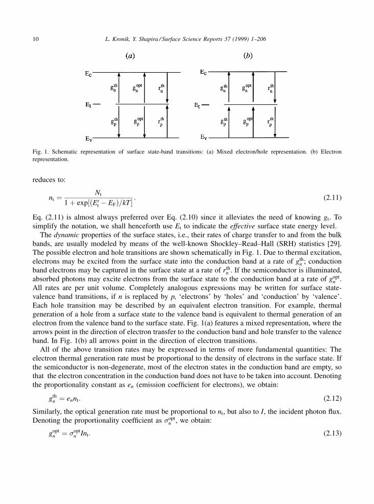
The dynamic properties of the surface states, i.e., their rates of charge transfer to and from the bulkbands, are usually modeled by means of the well-known Shockley±Read±Hall (SRH) statistics [29].The possible electron and hole transitions are shown schematically in Fig. 1. Due to thermal excitation,electrons may be excited from the surface state into the conduction band at a rate of gth
n ; conductionband electrons may be captured in the surface state at a rate of rth
n . If the semiconductor is illuminated,absorbed photons may excite electrons from the surface state to the conduction band at a rate of gopt
n .All rates are per unit volume. Completely analogous expressions may be written for surface state-valence band transitions, if n is replaced by p, `electrons' by `holes' and `conduction' by `valence'.Each hole transition may be described by an equivalent electron transition. For example, thermalgeneration of a hole from a surface state to the valence band is equivalent to thermal generation of anelectron from the valence band to the surface state. Fig. 1(a) features a mixed representation, where thearrows point in the direction of electron transfer to the conduction band and hole transfer to the valenceband. In Fig. 1(b) all arrows point in the direction of electron transitions.
All of the above transition rates may be expressed in terms of more fundamental quantities: Theelectron thermal generation rate must be proportional to the density of electrons in the surface state. Ifthe semiconductor is non-degenerate, most of the electron states in the conduction band are empty, sothat the electron concentration in the conduction band does not have to be taken into account. Denotingthe proportionality constant as en (emission coef®cient for electrons), we obtain:
gthn � ennt: (2.12)
Similarly, the optical generation rate must be proportional to nt, but also to I, the incident photon ¯ux.Denoting the proportionality coef®cient as �opt
n , we obtain:
goptn � �opt
n Int: (2.13)
Fig. 1. Schematic representation of surface state-band transitions: (a) Mixed electron/hole representation. (b) Electron
representation.
10 L. Kronik, Y. Shapira / Surface Science Reports 37 (1999) 1±206
The electron recombination rate depends on the conduction band electron density (per unit volume) atthe semiconductor surface, ns, but also on the density of available empty sites at the surface state, pt.Denoting the proportionality constant by cn (capture coef®cient for electrons), we obtain:
rthn � cnnspt: (2.14)
Again, analogous expressions may be formulated for the hole transition rates.The two parameters cn and en are not independent: Under thermal equilibrium (indexed by `0'), the
relation gthn0 � rth
n0 must be valid. Using Eqs. (2.12) and (2.14), and assuming cn and en are independentof surface-state occupation, we obtain:
en � cnns0pt0
nt0
� cnn1; (2.15)
where n1 is a proportionality constant measured by inverse volume units. The above assumption shouldbe approached with caution. For example, a large change in the electric ®eld may increase the effectiveemission rate considerably due to Poole±Frenkel emission and/or phonon-assisted tunneling. However,under most typical situations the emission/capture rates change by signi®cantly less than an order ofmagnitude [30]. Using Boltzmann statistics (appropriate for non-degenerate materials) for the variousquantities in Eq. (2.15) and its hole equivalent, one can additionally show that:
n1 � Nc exp�Et ÿ Ec�
kT
� �; p1 � Nv exp
�Ev ÿ Et�kT
� �; (2:16�
where Nc (Nv) is the effective density of states in the conduction (valence band).It can be further shown [31] that cn may be expressed in the form:
cn � knvn; (2.17)
where kn is de®ned as the thermal cross-section for electrons (and has units of area) and vn is theaverage electron thermal velocity. Relation (2.17) may be intuitively understood as follows. Thecapture cross-section should be proportional to the average electron thermal velocity. The largerthe latter is, the more volume the electron `covers' in a given time span and the larger is its proba-bility of getting caught in a surface state-related attractive potential. The thermal cross-section maytherefore be interpreted as the `effective target area' of the surface state. The probability of electroncapture is effectively approximated as one inside this area and zero outside it. Similarly, the �opt
n
coef®cient given in Eq. (2.13) may be de®ned as an optical cross-section ± the effective target area for aphoton to induce an electron transition to the conduction band. Both the thermal and optical cross-sections exhibit values which range over many orders of magnitude, depending on the charge of thestate involved and its exact potential structure. It is interesting to note that for an uncharged state, thethermal cross-section of a gap state is approximately the same as its physical cross-section ± about10ÿ15 cmÿ3 [30].
Under the model presented here, all surface-state properties of practical experimental interest may beexpressed in terms of six parameters: the surface-state density, energy level, electron and hole thermalcross-sections, and electron and hole optical cross-sections. Note that the thermal cross-sections maydepend on temperature and the optical cross-sections may depend on incident photon energy.
So far, only surface gap states have been discussed. However, a local defect in the bulk structure(e.g., an impurity atom, a vacancy, an interstitial atom, or an exchange in site between two different
L. Kronik, Y. Shapira / Surface Science Reports 37 (1999) 1±206 11

atoms) may also induce a localized gap state. If the surface state density and occupation in Eqs. (2.10)±(2.14) are replaced by volume densities, then the obtained relations are valid for a bulk defect gap stateas well. In fact, SRH statistics were ®rst developed for bulk defects [29]. An important application ofSRH statistics is determining the steady-state net recombination rate due to a defect gap state [31]. Insteady state, as opposed to equilibrium, the electron (or hole) generation and recombination terms donot have to cancel each other out since a net generation or recombination rate is possible. However,under steady-state conditions nt must remain constant, so that its net carrier exchange rate with theconduction band must be equal to that of the valence band, and is denoted by R. Using this conditionwith Eqs. (2.12) and (2.14) and solving for nt, we obtain:
nt � cnn� cpp1
cn�n� n1� � cp�p� p1�Nt: (2.18)
After some additional algebraic manipulation, the well-known SRH recombination expression isobtained:
R � npÿ n2i
�1=cpNt��n� n1� � �1=cnNt��p� p1� ; (2.19)
where in the case of surface recombination n; p should be replaced with ns; ps.In the case of bulk recombination, the coef®cients 1=�cnNt� and 1=�cpNt� have units of time and are
denoted by �n and �p, respectively. In the case of surface recombination, the same coef®cients haveunits of (velocity)ÿ1 and are denoted by sÿ1
n and sÿ1p , respectively. �n and �p are known as the minority
carrier lifetimes since, e.g., in the case of excess electrons in a p-type material and under theassumption of low injection (i.e., the number of excess carriers is much smaller than the original carrierconcentration), Eq. (2.19) reduces to:
R � �n
�n
: (2.20)
A similar expression exists for holes in an n-type material. Thus, �n��p� may be physically interpretedas the average `survival' time for an excess electron (hole) prior to its recombination. For surfacerecombination, we similarly obtain:
R � sn�ns: (2.21)
Here, sn � cnNt and sp � cpNt are known as the surface recombination velocities for minority carriers.Physically, if electrons moved towards the surface at a constant velocity, it should be equal to sn so thattheir rate of increase at the surface due to that motion would equal to the rate of their decrease at thesurface due to recombination. It is important to note that �n; �p or sn; sp only pertain to the case of lowlevel injection of minority carriers. For other cases, notably a high injection level and/or an intrinsicsemiconductor, different de®nitions of lifetimes or surface recombination velocities need to be used inEqs. (2.20) or (2.21). Therefore, one must exercise extreme caution when using a constant parameter,such as `lifetime' or `surface recombination velocity' as indicative of the properties of the bulk orsurface recombination rates under any conditions.
Finally, we note that the charge within any gap state is given by:
Qt � e�Nt ÿ nt�; for donor states; Qt � ÿent; for acceptor states: (2.22)
12 L. Kronik, Y. Shapira / Surface Science Reports 37 (1999) 1±206
For an energy distribution of gap states, Eq. (2.22) may be generalized to the form:
Qt � eX
d
�Ndt ÿ nd
t � ÿX
a
nat
" #; for discrete states (2.23a)
Qt � e
Zd
Ndt �E� ÿ nd
t �E�ÿ �
dE ÿZ
a
nat �E� dE
� �; for continuous states; (2.23b)
where the indices `d' and `a' denote donor and acceptor states, respectively. The effective optical andthermal cross-sections of a continuously distributed state may also be obtained by appropriate integrals.
2.1.3. Surface space charge region
The charge found in surface states is clearly supplied by the underlying bulk. We therefore expect thecarrier density in the vicinity of the surface to deviate from its equilibrium value and result in a surfacespace charge region (SCR). The surface may be found in three different regimes: (a) accumulation,where the majority carrier concentration at the surface is larger than its bulk value, (b) depletion, wherethe majority carrier concentration at the surface is smaller than its equilibrium value, but larger than theminority carrier concentration at the surface, and (c) inversion, where the majority carrier concentrationat the surface is smaller than the minority carrier concentration at the surface.
According to the Poisson equation (Eq. (2.1)), a non-equilibrium carrier density implies a non-zeroelectric ®eld and potential. Therefore, even under equilibrium conditions the surface potential, denotedas Vs, is different from the electric potential far away in the bulk. This means that the semiconductorbands are bent in the vicinity of the surface. By de®nition, the energy band is lower the higher theelectrical potential is, so that a positive Vs corresponds to downward-bent bands.
Within the scope of this review, we are interested primarily in Vs and not in the exact `shape' of thesurface SCR, i.e., the dependence of the electric potential on the coordinate [22±24]. The reason is thatonly Vs, and not the entire potential pro®le, is measured in a surface photovoltage experiment, asdescribed in detail in the next section and chapter. For a given set of semiconductor bulk and surfaceproperties, the value of Vs is dictated by the charge conservation rule:
Qss � ÿQsc; (2.24)
where Qss is the net surface charge and Qsc is the net charge in the SCR (both per unit area). This isbecause the underlying crystal is the sole supplier of the surface charge. For calculating Vs, we mustknow how Qss and Qsc depend on it.
We start with the dependence of Qss on Vs as it is quite simply derived from Fermi±Dirac statistics:Since the surface states have a ®xed energy distance from the band edges, their energy distance fromthe Fermi level changes in the presence of band bending. We denote the Fermi-level to state-energyinterval in the absence of band bending by �Et ÿ EF�0. Then:
Qss � eNt 1ÿ 1
1� exp Et ÿ EF� �0ÿeVs
ÿ �=kT
� �( ); for a donor state: (2.25a)
Qss � ÿeNt
1
1� exp Et ÿ EF� �0ÿeVs
ÿ �=kT
� � ; for an acceptor state: (2.25b)
L. Kronik, Y. Shapira / Surface Science Reports 37 (1999) 1±206 13
If multiple states are present, the total charge may be found by summation and integration as inEq. (2.23). Note that Qss may also have a ®xed (and hence Vs independent) component which is theresult of adsorbed ionized species.
We now consider the dependence of Qsc on Vs, based on the treatment by Sze [25]. We focus ourattention on a p-type semiconductor because the results for an n-type semiconductor may be easilycompleted by analogy. In the presence of both donors and acceptors, the total (static and dynamic)charge density may be expressed as:
��x� � e�Nd ÿ Na � pÿ n�; (2.26)
where Nd �Na� is the donor (acceptor) density, assumed to be uniform. If the semiconductor is non-degenerate, we obtain the relation of the electron and hole densities in the SCR to their densities in thequasi-neutral bulk from the Boltzmann relations (Eq. (2.7)):
n�x� � nb expeV�x�
kT
� �; p�x� � pb exp
ÿeV�x�kT
� �: (2.27)
Moreover, in the quasi-neutral region the net charge density is zero so that:
Nd ÿ Na � nb ÿ pb; (2.28)
where the index `b' denotes the bulk. Placing expressions (2.26)±(2.28) in the Poisson equation(Eq. (2.1)) we obtain:
d2V
dx2� ÿ e
�� pb�eÿeV=kT ÿ 1� ÿ nb�eeV=kT ÿ 1��: (2.29)
We denote the position of the surface by x � 0, with the semiconductor extending towards the positive xaxis. We choose the potential at in®nity as zero. Because at in®nity the semiconductor is quasi-neutral,the electric ®eld, E, which by de®nition equals ÿdV=dx, must also be zero there.
For obtaining an explicit expression for Qsc, Eq. (2.29) is integrated from the bulk toward the surfaceusing the above boundary conditions, yielding an expression for the surface electric ®eld, Es. Once Es isknown, Qsc is obtained by using the relation Qsc � ÿ�sEs. The latter relation is a direct result of theGauss theorem, where one side of the Gauss surface is located at the quasi-neutral region and the otherat x � 0�, i.e., just outside the semiconductor surface. The ®nal result of this procedure is:
Qsc � ����2p
�skT
eLD
FeV
kT;nb
pb
� �; (2.30)
where LD �������������������������kT�s=�e2pb�
pis the Debye screening length (for holes, in this case) and:
FeV
kT;nb
pb
� �� eÿeV=kT � eV
kTÿ 1
� �� nb
pb
eeV=kT ÿ eV
kTÿ 1
� �� �1=2
; (2.31)
where the positive (negative) sign corresponds to Vs > 0 �Vs < 0�.Vs may be found by solving Eq. (2.24), where the left hand side is replaced by Eq. (2.25) and the
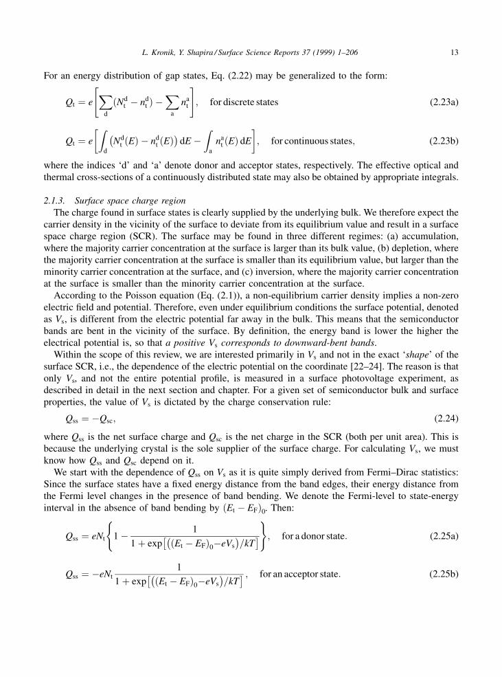
right hand side is replaced by Eq. (2.30). Much physical intuition is obtained if this solution isperformed graphically by plotting both Qss and Qsc versus Vs on the same graph [23,32,33]. An exampleis shown in Fig. 2, which features such a graphical solution for a hypothetical 1016 cmÿ3 p-type InPsample with surface donor states of varying density and energy position. All three regimes discussedabove ± accumulation, depletion, and inversion ± are clearly manifested in the Qsc versus Vs curve. The
14 L. Kronik, Y. Shapira / Surface Science Reports 37 (1999) 1±206

three regimes are easily distinguished because they are dominated by different terms in Eq. (2.31). Inthe accumulation and inversion regimes, the ®rst and fourth terms in Eq. (2.31) dominate, respectively.Hence, Qscj j ' exp�e Vsj j=2kT� in both cases. In the depletion regime, however, the second termdominates and thus Qscj j ' ��������
Vsj jp
.The graphical solution also demonstrates that the higher surface state density is, the larger the band
bending is. This is because more charge transfer from surface to bulk is necessary for achievingequilibrium. In addition, the higher the donor state is within the bandgap, the larger the band bending isbecause a larger change in the surface Fermi level position is required for the surface state population tochange appreciably.
Several additional comments are in order. First, in the depletion regime the same square rootdependence obtained from Eq. (2.31) would have been obtained had mobile charges been neglected apriori. An often used approximation, known as the depletion approximation, assumes that the region inwhich the mobile carriers are negligible ends abruptly at a distance w from the surface. Hence:
Qscj j ' e Na ÿ Ndj jw; (2.32)
Combining Eq. (2.32) with the form of Eq. (2.30) appropriate for the depletion regime one obtains:
w ����������������������
2�sVs
e Na ÿ Ndj j
s: (2.33)
For reasonable values, e.g., Vs � 0:4 V, �s � 11:8�0 (silicon), and Na ÿ Ndj j � 5� 1015 cmÿ3, weobtain w � 0:3 mm. This result reveals the striking in¯uence of surface states on the semiconductorbulk: states localized over no more than several monolayers affect the semiconductor electrically evenseveral thousand monolayers away from the surface.
Fig. 2. Graphical determination of Vs for a hypothetical 1016 cmÿ3 p-type InP sample with surface denor states. Solid curve:
Dependence of jQscj on Vs. Dashed curves: Dependence of Qss on Vs with (a) Nt � 1012 cmÿ2, (Et ÿ EF�0 � 0:5 eV. (b)
Nt � 1012 cmÿ2, (Et ÿ EF�0 � 0:7 eV. (c) Nt � 2 � 1011 cmÿ2, (Et ÿ EF�0 � 0:5 eV:
L. Kronik, Y. Shapira / Surface Science Reports 37 (1999) 1±206 15

Second, Eq. (2.30) is recast in several equivalent mathematical forms in the literature. A commonone is the one given by Kingston and Neustadter [34], who have solved the Poisson equation (Eq. (2.1)),where the mobile charge densities are expressed in terms of the energy distance between the Fermilevel and the intrinsic Fermi level, normalized to kT=e, namely:
n � nieÿu; p � nie
u; where u � e EF ÿ EFi� �kT
: (2.34)
Using the same approach outlined above, they obtained:
Qsc � ����2p
�skT
eLD
F us; ub� �; (2.35)
where LD ������������������������kT�s=�e2ni�
pis the intrinsic Debye screening length and F us; ub� � � sinh ub ub ÿ us� �ÿ�
cosh ub ÿ cosh us� ��1=2. The subscripts `s' and `b' have their usual meaning of surface and bulk,
respectively, and Vs � �kT=e� � �us ÿ ub�. It should be emphasized that Eqs. (2.30) and (2.35) areabsolutely equivalent. Like Eqs. (2.3) and (2.9), they are the charge densities and Fermi level positionrepresentations, respectively. Other hybrid forms of Eqs. (2.30) and (2.35) are also commonly used inthe literature.
Third, the detailed analysis presented above may be readily extended to cover more general cases atthe expense of more complicated mathematics. For example, if the semiconductor is degenerate theexpressions in Eq. (2.27) must be replaced by the appropriate Fermi±Dirac expressions [23,24]. When avery strong accumulation or inversion is obtained, majority or minority carriers, respectively, arecon®ned in a very narrow layer. Under such conditions they are typically considered in terms of a two-dimensional carrier gas. The semi-classical approach presented here then fails and one must resort to asimultaneous solution of the Poisson and SchroÈdinger equations [23,24].
Fourth, another generalization of particular importance arises when the semiconductor bulk containsa non-negligible amount of deep acceptors or donors (or when the temperature is suf®ciently low so thatnot all of the shallow donors/acceptors are completely ionized). In this case, the appropriate donor andacceptor terms in Eq. (2.26) should not be taken as constant but rather should be represented by chargeterms similar to Eq. (2.25) (for volume densities, of course) [22]. The effect of deep states is usuallynegligible in the accumulation and inversion regimes, where Eq. (2.26) is dominated by mobile, ratherthan static, charges. However, it may be very signi®cant in the depletion regime [35].
2.1.4. Surface dipoles
In addition to surface states, another important phenomenon associated with a semiconductor surfaceis the surface dipole. Despite its importance, this phenomenon has received considerably less attentionthan surface state phenomena. Since surface dipole considerations play an important role in someanalyses of SPV experiments, it is the purpose of this sub-section to introduce the relevant concepts inan orderly manner.
At a free surface, a `tail' of the surface-localized electron wave functions `spills out' into thevacuum. Therefore, the region just outside the surface has a net negative charge, whereas the region justinside the surface is left with a net positive charge [36]. The separation of positive and negative chargesover atomic distances is, by de®nition, a microscopic dipole. This dipole creates a ®eld which opposesfurther electron transfer into the vacuum. Electrons reaching the surface are repelled by the negative
16 L. Kronik, Y. Shapira / Surface Science Reports 37 (1999) 1±206
charge outside the material and attracted by the positive charge inside the material. Thus, an abruptpotential barrier for electrons attempting to leave the semiconductor is formed. This barrier is usuallycharacterized by means of the electron af®nity, �, de®ned as the energy needed to release an electronfrom the conduction band into vacuum.
At a real semiconductor surface, the effective surface barrier is not determined solely by the `spill-out effect'. Many additional microscopic dipole contributions are possible due to different surfaceeffects. As noted in Section 2.1.2, the surface may be relaxed or reconstructed. The exact arrangementof the atomic positions may affect the `center of gravity' of the charge in the chemical bond betweenthe atoms and hence create a surface dipole. Moreover, a change in atomic positions may create an`electron smoothing-out effect' in which for a more open surface, electron wave function tails tend to`®ll in' the gaps between atoms, another cause for a surface dipole [36]. Ranke and co-workers haveshown that the effective electron af®nity undergoes notable changes with surface orientation for Si, Ge,and GaAs [37]. They concluded that in these cases the atomic contribution dominates over theelectronic contribution to the surface dipole. Local stoichiometry changes at the semiconductor surfacemay also create a surface dipole. An adsorbate layer may also result in a surface dipole, the magnitudeof which depends on the ionicity of the adsorbate±substrate bond. The ionicity is related to thedifference in electronegativity between the adsorbate species and the semiconductor substrate [11].Partial charge transfer between the adsorbate and a gap state may likewise cause a surface dipole and isalso governed by the degree of ionicity of the bond [11].
As in the case of gap states, a dipole layer is not limited to semiconductor surfaces, but also appearsat semiconductor interfaces. Any change in the structure and/or chemistry of interface atoms withrespect to bulk ones may result in an interface dipole. For example, Nicolini et al. have shown, boththeoretically and experimentally, that the local Zn/Se relative concentration at the heterovalent ZnSe/GaAs(0 0 1) interface has a direct in¯uence on the dipole at that interface [38]. Partial charge transferat a metal/semiconductor or a semiconductor/semiconductor interface (e.g., due to `tails' of interfacestate wave functions) may also result in an interface dipole [39±41].
Lambrecht et al. [41] have correctly pointed out that the term `interface dipole' has been used ratherliberally in the literature with different and ambiguous de®nitions by different authors. In order tounequivocally de®ne the terminology used in this article, we invoke the concept of a local vacuumlevel, El, de®ned (following Marshak [42]) as the energy of an electron at a given point if it were atrest and free from the in¯uence of the crystal potential (which determines the band structure). It isimportant to understand the difference between the local and the absolute vacuum level: The absolutevacuum level is de®ned as the reference energy of an electron at rest which is situated very far from thesemiconductor so that it is `unaware' of the existence of the semiconductor. At the local vacuum level,the electron at rest is free from the crystal microscopic potentials caused by the atomic forces, but notfrom macroscopic potentials, e.g., those due to the electric ®eld at a SCR.
The local vacuum level concept may also be understood by the following `gedanken' experiment:Suppose electrons are liberated from the conduction band of a hypothetical semiconductor sample,which consists of a p±n homojunction buried deep within the sample. Furthermore, suppose that thesurfaces are ideal so that the only SCR is due to the p±n junction, as in Fig. 3 and that the two surfacesare exactly equivalent, so they have the same effective electron af®nity. Consequently, the twoelectrons, liberated into vacuum from the conduction band at both sides of the junction, must haveenergies differing by the amount of energy necessary to overcome the potential barrier so as to bring theelectron from one surface to the other. Hence, it is clear that the local vacuum level must follow any
L. Kronik, Y. Shapira / Surface Science Reports 37 (1999) 1±206 17

changes in the electric potential along the sample. This reasoning naturally leads to the de®nition of theelectron af®nity as � � El ÿ EC. According to this de®nition, � is really a bulk quantity in the sensethat it is the amount of energy necessary to remove an electron from the conduction band at a pointinside the crystal into vacuum. However, in reality it is, of course, impossible to remove an electron intovacuum without ®rst bringing it to the surface. At the surface, the effective electron af®nity, �� , maydiffer from that of the bulk due to the various surface dipole effects discussed above. A completeschematic band diagram of a semiconductor surface SCR is shown in Fig. 4. Using the ®gure, weobserve that the surface dipole, ��s, manifests itself as a step in the local vacuum level, i.e., in theelectric potential at the surface because the potential changes abruptly over several monolayers. This isin contrast to the macroscopic dipole created by the surface states and surface SCR, also shown inFig. 4. In the latter case, the average separation between the positive �Qss� and the negative �Qsc�charges is not on an atomic scale, and the electric potential changes gradually. For consistency with thesign convention of the surface voltage, we de®ne the surface dipole as positive if the local vacuum leveldrops when passing from the semiconductor into vacuum. Thus, the dipole is positive if its positive sidepoints outwards. Using Fig. 4, we also de®ne the work function at the semiconductor surface in
Fig. 3. Schematic diagram of the local vacuum level in a hypothetical p±n junction.
Fig. 4. Schematic diagram of the electronic band structure at a semiconductor surface.
18 L. Kronik, Y. Shapira / Surface Science Reports 37 (1999) 1±206
equilibrium, Ws, as the energy separation between the Fermi level and the local vacuum level at thesurface. Ws may be expressed in the form:
Ws � Ec ÿ EF� �bÿeVs � �ÿ��s � Ec ÿ EF� �bÿeVs � ��: (2.36)
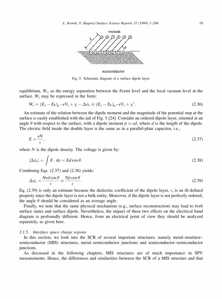
An estimate of the relation between the dipole moment and the magnitude of the potential step at thesurface is easily established with the aid of Fig. 5 [24]. Consider an ordered dipole layer, oriented at anangle � with respect to the surface, with a dipole moment �p � ed, where d is the length of the dipole.The electric ®eld inside the double layer is the same as in a parallel-plate capacitor, i.e.,
E � eN
�; (2.37)
where N is the dipole density. The voltage is given by:
��sj j �Z
E � dx � Ed cos �: (2.38)
Combining Eqs. (2.37) and (2.38) yields:
��s � Ned cos �
�� N�p cos �
�: (2.39)
Eq. (2.39) is only an estimate because the dielectric coef®cient of the dipole layer, �, is an ill-de®nedproperty since the dipole layer is not a bulk entity. Moreover, if the dipole layer is not perfectly ordered,the angle � should be considered as an average angle.
Finally, we note that the same physical mechanism (e.g., surface reconstruction) may lead to bothsurface states and surface dipole. Nevertheless, the impact of these two effects on the electrical banddiagram is profoundly different. Hence, from an electrical point of view they should be analyzedseparately, as given here.
2.1.5. Interface space charge regions
In this section, we look into the SCR of several important structures, namely metal±insulator±semiconductor (MIS) structures, metal±semiconductor junctions and semiconductor±semiconductorjunctions.
As discussed in the following chapters, MIS structures are of much importance in SPVmeasurements. Hence, the differences and similarities between the SCR of a MIS structure and that
Fig. 5. Schematic diagram of a surface dipole layer.
L. Kronik, Y. Shapira / Surface Science Reports 37 (1999) 1±206 19

of a free surface merit some elaboration. A MIS structure consists of an insulating layer sandwichedbetween a metallic layer and a semiconducting material. The insulating layer may be solid but may alsobe simply air or vacuum. The metallic layer is connected to the back side of the semiconductingmaterial via an external voltage source.
Even if surface states are not present anywhere in the structure and the external voltage source is setat null, a SCR is still expected in the semiconducting material, extending from the semiconductor-insulator interface into the bulk of the semiconductor. The reason is that due to the different workfunctions of the semiconductor and the metal, charge must be transferred between them in order fortheir Fermi levels to equilibrate. A schematic band diagram of such a structure `before' and `after' theestablishment of a contact between metal and semiconductor in this ideal case is given in Figs. 6(a),(b),respectively. The surface SCR is further affected if surface states do exist, as discussed in Section 2.1.3above, as well as by an external bias between the metal and semiconductor. Thus, it is necessary to ®ndout how to calculate the surface voltage in the general case, a schematic band diagram of which(neglecting interface dipoles) is given in Fig. 6(c).
In the MIS case, Eq. (2.24), the charge neutrality condition of the free surface, is replaced by themore general charge neutrality condition:
Qm � Qsc � Qss � 0; (2.40)
where Qm is the charge density on the metal±insulator surface. However, Eqs. (2.25) and (2.30),describing the dependence of Qss and Qsc, respectively, on Vs are still valid. Using the Gauss theorem it
Fig. 6. Schematic band diagram of a MIS structure: (a) No surface states, before metal±semiconductor contact. (b) No surface
states, after contact, with zero external bias, (c) general case, with non-zero external bias.
20 L. Kronik, Y. Shapira / Surface Science Reports 37 (1999) 1±206

is easy to ®nd that:
Qm � �insEins � �insVins
dins
� Qm � CinsVins; (2.41)
where �ins;Eins;Vins; dins, and Cins are the dielectric permittivity, electric ®eld, voltage, thickness, andcapacitance per unit area of the insulating layer, respectively. Furthermore, using Fig. 2.6(c), we ®ndthe relation:
ÿeVins � eVs � �m ÿ �s ÿ eVG; (2.42)
where �m is the metal work function, �s the work function of the semiconductor in the absence of bandbending, and VG the external bias. Note that dipoles present at any interface induce steps in the localvacuum level in the band diagram of Fig. 6(c). However, those are usually overlooked in the MISliterature because they are typically absorbed in �m ÿ �s. Expressing Qm as an explicit function of Vs
via Eqs. (2.41) and (2.42), Eq. (2.40) may be reduced to an equation for Vs alone.Note that Eq. (2.41) shows that the charge on the metal decreases with decreasing insulator
capacitance. This means that in the case of a vacuum or air gap, Vs of the free surface and Vs of the MISstructure are practically identical if the metal is suf®ciently removed from the surface because Qm isnegligible, so that Eq. (2.40) reduces to Eq. (2.24).
We next discuss rectifying metal±semiconductor junctions [25]. (Ohmic metal±semiconductorjunctions are not considered here since usually no signi®cant space charge effects are associated withthem). Such junctions may be thought of as a limiting case of the MIS structure, with the thickness ofthe insulating layer approaching zero. The limiting case in the absence of interface states (known as theSchottky limit) is shown in Fig. 7(a). A potential barrier, �b, known as the Schottky barrier, is formedbetween the metal and the semiconductor and is responsible for the rectifying properties of the junction.Using Fig. 7(a), it is clear that in this limit, for the n-type semiconductor depicted in the diagram,�b � �m ÿ �.
The extreme opposite case, where there is a very high density of interface states (known as theBardeen limit), is depicted in Fig. 7(b). Here, the interface state density is large enough so that thechange in surface voltage when moving from the free semiconductor surface to the metal±semiconductor interface is practically negligible since Qm � Qss (assuming, of course, that the natureof the surface and interface states is the same). In such a case, the Fermi level at the interface is referred
Fig. 7. Schematic band diagram of a rectifying metal±semiconductor junction: (a) No interface states (Schottky limit), (b)
High interface state density (Bardeen limit).
L. Kronik, Y. Shapira / Surface Science Reports 37 (1999) 1±206 21

to as `pinned' by the interface states since it has approximately the same value, regardless of the metaltype. Similarly, the surface Fermi level is independent of metal type and spacing in a MIS structure if`pinned' by a high density of interface states. Fig. 7(b) shows that the Schottky barrier is given by theenergy interval between the pinned Fermi level position and the conduction band at the surface and notby the ideal relation. Hence, an interface dipole, ��in, must be present. This dipole is physicallybrought about because Qss and Qm are separated by an atomic distance. Note that in this case the samecharge, Qss, is responsible for the interface charge (and hence the SCR), as well as the interface dipole(together with Qm). Cowley and Sze [43] have forwarded a more general model, where the Schottkybarrier height is determined as a linear combination of the Schottky and Bardeen limits. In practice, thevalue of the Schottky barrier may be further complicated by various physical and chemical phenomena,such as metal and semiconductor interdiffusion, chemical reactions, lateral junction non-uniformities,etc. Thus, metal±semiconductor junctions still attract a considerable amount of theoretical andexperimental research, the results of which are described in detail elsewhere (see, e.g., [7,44]). Inpractice, �b is determined experimentally.
We now move to the band diagram of semiconductor heterojunctions. In these structures, theparameters most pertinent to the electrical behavior of the heterojunction are the conduction andvalence band offsets, �Ec and �Ev, respectively. These parameters control the height of the potentialbarrier (or drop) encountered by electrons or holes trying to traverse the heterojunction interface. As anexample, we consider a heterojunction where the larger bandgap material is p-type and the smallerbandgap material is n-type, with no loss of generality. Such a band lineup, with and without an interfacedipole, is shown in Figs. 8(a) and (b), respectively. We adopt the following sign convention for the bandoffsets. In accordance with the sign conventions for the built-in voltage and the interface dipole, �Ec isalso de®ned as positive if the bottom of the conduction band drops on passing from Material 1 to 2.However, �Ev is negative if the top of the valence band drops on passing from Material 1 to 2. Thelatter sign convention implies the relation:
�Ec ��Ev � �Eg � Eg1 ÿ Eg2; (2.43)
where Eg is the semiconductor bandgap. Note that using this sign convention �Ec may be assigned
Fig. 8. Schematic energy band lineup at a type I semiconductor heterojunction: (a) without an interface dipole, (b) with a non-
zero interface dipole.
22 L. Kronik, Y. Shapira / Surface Science Reports 37 (1999) 1±206

either a negative or a positive value, depending on whether the larger bandgap material is referred to as`Material 1' or `2'. Thus, it can be made equivalent to any sign convention used in the literature. Eq.(2.43) implies that if �Ec and the bandgap energies are known, so is �Ev. Hence, we focus ourattention on �Ec.
In the absence of an interface dipole (Fig. 8(a)) and for uniform bulk materials, �Ec is equal to�2 ÿ �1. This equality is known as the Anderson rule [45]. In many cases this rule is not followedexperimentally. One reason for this is the presence of an interface dipole (Fig. 8(b)), which modi®es theAnderson rule to �Ec � �2 ÿ �1 ���in. Interestingly, a heterojunction band diagram which includesan interface dipole and a local vacuum level as de®ned in the present text, was proposed by Van Ruyvenas early as 1964 [46]. Moreover, in a real experiment one measures the effective electron af®nity, ��,and not the electron af®nity as de®ned using the local vacuum level concept. Thus, the electron af®nityvalues used in the Anderson rule may lead to results which are in disagreement with experiment, evenin the absence of an interface dipole. This may explain why 35 years after Anderson's original paper,the accurate and direct determination of the band offsets in a heterojunction under study is still achallenge [47].
Using Fig. 8, �Ec may also be expressed as:
�Ec � Ec ÿ EF� �b1ÿeVb1
� �ÿ Ec ÿ EF� �b2�eVb2
� �; (2.44)
where Vb is the potential drop on one side of the heterojunction and all other indices have their usualmeaning. The built-in voltage, Vbi, is by de®nition the total voltage drop across the interface SCR:
Vbi � Vb1 � Vb2 ���in: (2.45)
Hence, Eqs. (2.44) and (2.45) may be combined to yield:
�Ec � Ec1 ÿ Ec2 ÿ eVbi ���in: (2.46)
An interface SCR also obeys the charge neutrality law, given by:
Q1 � Q2 � Qss � 0; (2.47)
where Q1 and Q2 are the charge densities (per unit area) on both sides of the interface.Even in the absence of interface states, an interface dipole induces a SCR (in marked contrast to a
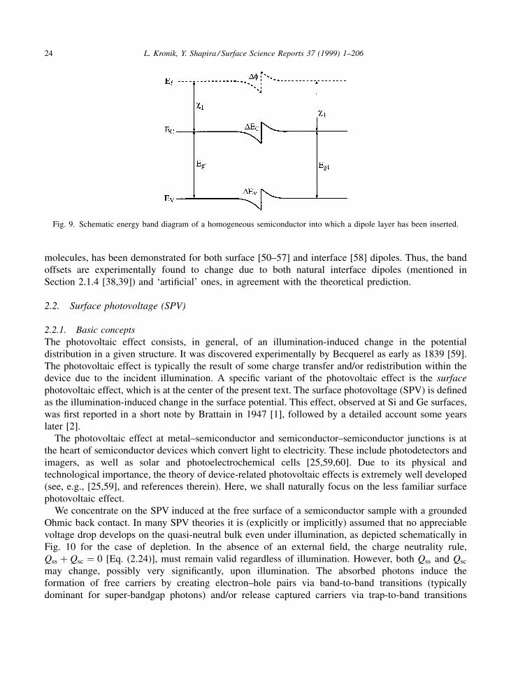
surface dipole). Consider another gedanken experiment, shown in Fig. 9, in which an interface dipole is`inserted' at a p±n homojunction. The abrupt discontinuity in the local vacuum level dictated by thedipole layer, combined with the necessarily identical electron af®nities far away from the interface,imply that the local vacuum level must be bent. Thus, an electrostatic potential develops and aninterface SCR is formed. Physically, insertion of an interface dipole in a uniform semiconductor sampleforces the electrons on one side of the dipole to have an average energy which is higher than those onthe other side. This induces electron transfer from the high energy to the low energy side, setting up aninternal electric ®eld to counteract the ¯ow. In the case of a surface dipole, there are no electrons on thevacuum side and hence this phenomenon is absent.
The insertion of an `arti®cial dipole layer' is by no means only a thought experiment. The bandoffsets of many heterojunctions have been modi®ed by means of inserting thin intralayers of a differentmaterial at the interface, which create a net interface dipole [48]. Similarly, an arti®cial banddiscontinuity was induced at a GaAs homojunction by means of inserting a very thin Si intralayer [49].An interesting different approach, which modi®es the dipole by means of a chemical bond with organic
L. Kronik, Y. Shapira / Surface Science Reports 37 (1999) 1±206 23
molecules, has been demonstrated for both surface [50±57] and interface [58] dipoles. Thus, the bandoffsets are experimentally found to change due to both natural interface dipoles (mentioned inSection 2.1.4 [38,39]) and `arti®cial' ones, in agreement with the theoretical prediction.
2.2. Surface photovoltage (SPV)
2.2.1. Basic concepts
The photovoltaic effect consists, in general, of an illumination-induced change in the potentialdistribution in a given structure. It was discovered experimentally by Becquerel as early as 1839 [59].The photovoltaic effect is typically the result of some charge transfer and/or redistribution within thedevice due to the incident illumination. A speci®c variant of the photovoltaic effect is the surface
photovoltaic effect, which is at the center of the present text. The surface photovoltage (SPV) is de®nedas the illumination-induced change in the surface potential. This effect, observed at Si and Ge surfaces,was ®rst reported in a short note by Brattain in 1947 [1], followed by a detailed account some yearslater [2].
The photovoltaic effect at metal±semiconductor and semiconductor±semiconductor junctions is atthe heart of semiconductor devices which convert light to electricity. These include photodetectors andimagers, as well as solar and photoelectrochemical cells [25,59,60]. Due to its physical andtechnological importance, the theory of device-related photovoltaic effects is extremely well developed(see, e.g., [25,59], and references therein). Here, we shall naturally focus on the less familiar surfacephotovoltaic effect.
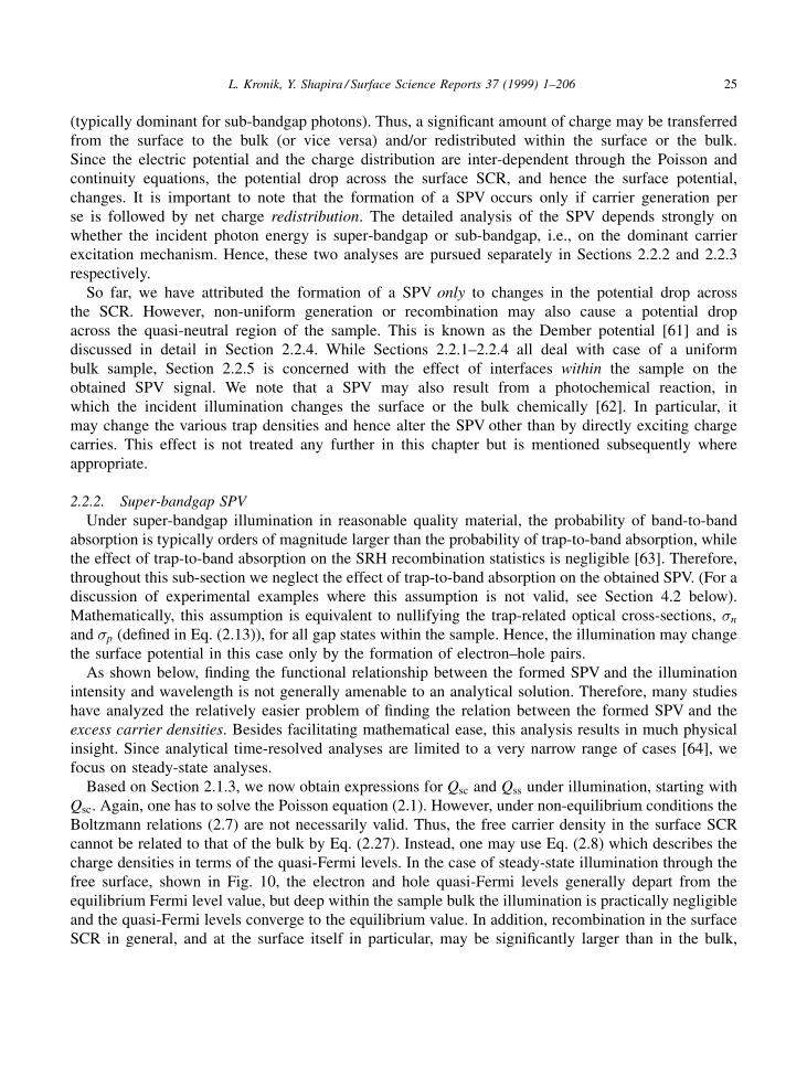
We concentrate on the SPV induced at the free surface of a semiconductor sample with a groundedOhmic back contact. In many SPV theories it is (explicitly or implicitly) assumed that no appreciablevoltage drop develops on the quasi-neutral bulk even under illumination, as depicted schematically inFig. 10 for the case of depletion. In the absence of an external ®eld, the charge neutrality rule,Qss � Qsc � 0 [Eq. (2.24)], must remain valid regardless of illumination. However, both Qss and Qsc
may change, possibly very signi®cantly, upon illumination. The absorbed photons induce theformation of free carriers by creating electron±hole pairs via band-to-band transitions (typicallydominant for super-bandgap photons) and/or release captured carriers via trap-to-band transitions
Fig. 9. Schematic energy band diagram of a homogeneous semiconductor into which a dipole layer has been inserted.
24 L. Kronik, Y. Shapira / Surface Science Reports 37 (1999) 1±206
(typically dominant for sub-bandgap photons). Thus, a signi®cant amount of charge may be transferredfrom the surface to the bulk (or vice versa) and/or redistributed within the surface or the bulk.Since the electric potential and the charge distribution are inter-dependent through the Poisson andcontinuity equations, the potential drop across the surface SCR, and hence the surface potential,changes. It is important to note that the formation of a SPV occurs only if carrier generation perse is followed by net charge redistribution. The detailed analysis of the SPV depends strongly onwhether the incident photon energy is super-bandgap or sub-bandgap, i.e., on the dominant carrierexcitation mechanism. Hence, these two analyses are pursued separately in Sections 2.2.2 and 2.2.3respectively.
So far, we have attributed the formation of a SPV only to changes in the potential drop acrossthe SCR. However, non-uniform generation or recombination may also cause a potential dropacross the quasi-neutral region of the sample. This is known as the Dember potential [61] and isdiscussed in detail in Section 2.2.4. While Sections 2.2.1±2.2.4 all deal with case of a uniformbulk sample, Section 2.2.5 is concerned with the effect of interfaces within the sample on theobtained SPV signal. We note that a SPV may also result from a photochemical reaction, inwhich the incident illumination changes the surface or the bulk chemically [62]. In particular, itmay change the various trap densities and hence alter the SPV other than by directly exciting chargecarries. This effect is not treated any further in this chapter but is mentioned subsequently whereappropriate.
2.2.2. Super-bandgap SPV
Under super-bandgap illumination in reasonable quality material, the probability of band-to-bandabsorption is typically orders of magnitude larger than the probability of trap-to-band absorption, whilethe effect of trap-to-band absorption on the SRH recombination statistics is negligible [63]. Therefore,throughout this sub-section we neglect the effect of trap-to-band absorption on the obtained SPV. (For adiscussion of experimental examples where this assumption is not valid, see Section 4.2 below).Mathematically, this assumption is equivalent to nullifying the trap-related optical cross-sections, �n
and �p (de®ned in Eq. (2.13)), for all gap states within the sample. Hence, the illumination may changethe surface potential in this case only by the formation of electron±hole pairs.
As shown below, ®nding the functional relationship between the formed SPV and the illuminationintensity and wavelength is not generally amenable to an analytical solution. Therefore, many studieshave analyzed the relatively easier problem of ®nding the relation between the formed SPV and theexcess carrier densities. Besides facilitating mathematical ease, this analysis results in much physicalinsight. Since analytical time-resolved analyses are limited to a very narrow range of cases [64], wefocus on steady-state analyses.
Based on Section 2.1.3, we now obtain expressions for Qsc and Qss under illumination, starting withQsc. Again, one has to solve the Poisson equation (2.1). However, under non-equilibrium conditions theBoltzmann relations (2.7) are not necessarily valid. Thus, the free carrier density in the surface SCRcannot be related to that of the bulk by Eq. (2.27). Instead, one may use Eq. (2.8) which describes thecharge densities in terms of the quasi-Fermi levels. In the case of steady-state illumination through thefree surface, shown in Fig. 10, the electron and hole quasi-Fermi levels generally depart from theequilibrium Fermi level value, but deep within the sample bulk the illumination is practically negligibleand the quasi-Fermi levels converge to the equilibrium value. In addition, recombination in the surfaceSCR in general, and at the surface itself in particular, may be signi®cantly larger than in the bulk,
L. Kronik, Y. Shapira / Surface Science Reports 37 (1999) 1±206 25
thereby reducing the effective excess carrier density. This may cause the quasi-Fermi levels to deviateless from equilibrium towards the surface than at the edge of the SCR, as in Fig. 10. According toEq. (2.9), changes in the quasi-Fermi levels indicate a non-zero electron and hole current, even understeady-state conditions. Indeed, under open circuit conditions only the total current, J, must be zero,whereas Jn and Jp may be non-zero. This does not contradict the principle of detailed balance [31],which only demands that Jn and Jp provide carriers at a rate which maintains a steady state surfacerecombination rate, i.e., Jn�0� � ÿJp�0� � eRs, where Rs � Rn � Rp is the steady-state surfacerecombination rate.
In 1955, Garrett and Brattain have published a classic paper [3], where a ®rst serious attempt wasmade at a comprehensive theory of semiconductor surfaces, including surface photovoltaic effects.They suggested that under certain conditions, the quasi-Fermi levels may be approximated as position-independent (i.e., `¯at') throughout the surface SCR. They identi®ed two conditions for thisapproximation to hold. First, the SCR width must be considerably smaller than the (electron and hole)diffusion length, L, so that the effect of non-uniform carrier excitation is negligible over the SCR. Thiscondition is quite easily satis®ed in many materials of reasonable quality. Second, the defect-relatedrecombination current must not be `too large' nor the depletion of carriers `too extreme' [3]. The latterconditions assure that even if Jn , Jp are not zero, the variation in the quasi-Fermi levels, Fn and Fp,given by [see Eq. (2.9)]:
dFn
dx
���� ���� � Jn
n�n
;dFp
dx
���� ���� � Jp
p�p
; (2.48)
may be neglected. For understanding this point further, consider the order of magnitude calculationgiven by Many et al. [22]. Neglecting recombination in the SCR, the recombination current is constantthroughout the SCR and is equal to eRs, where Rs is given by Eq. (2.19). In the case of a depleted p-typesemiconductor, it can be shown that Rs is always smaller than cpNtps and p always larger than ps. Thus,using Eq. (2.48) we obtain:
dFp
dx
���� ���� � cpNt
�p
) �Fp � cpNtw
�p
; (2.49)
where �Fp is the variation of the hole quasi-Fermi level across the entire SCR For, e.g., a Si samplewith w � 0:4 mm , cp � 10ÿ8 cm3/s, and Nt � 1012 cmÿ2, we get �Fp < 1 meV, which, except at verylow temperatures, is much smaller than kT and therefore negligible. Similar considerations apply to theelectron quasi-Fermi level.
Fig. 10. Schematic band diagram of a surface space charge region under depletion: Solid lines ± equilibrium. Dashed lines ±
under illumination. Dash-dotted lines ± quasi-Fermi levels under illumination.
26 L. Kronik, Y. Shapira / Surface Science Reports 37 (1999) 1±206
Frankl [65] has performed more detailed estimates of the validity of the ¯at quasi-Fermi levels (FQL)approximation. By making various approximations and assumptions regarding on the space chargefunction F (Eq. (2.31)), he has shown that for a depleted semiconductor with a reasonable SRV, theFQL approximation is typically acceptable as long as the illumination intensities are not too high (sincethis may result in a too large recombination current). Furthermore, Frankl has shown that theapproximation may fail for minority carriers in an accumulation layer and for majority carriers in aninversion layer [65]. Note that in both cases the change in carrier concentration with respect to the bulkvalue is `too extreme', as noted above. Following the results of the ®rst-order calculations of Many etal., as well as the more detailed quantitative work of Frankl, we adopt the Garrett±Brattainapproximation for further considerations.
Assuming that Fn and Fp are position independent, the dependence of Qsc on the minority carrierdensity at the edge of the SCR is relatively easily found. This is because under this assumption theBoltzmann relations (2.7), and hence Eq. (2.26) hold even for non-equilibrium densities, i.e.,
n��x� � n�b expeV�x�
kT
� �; p��x� � p�b exp
ÿeV�x�kT
� �; (2.50)
where here and in the following the superscript `*' denotes non-equilibrium densities and n�b and p�b,refer to the charge density at the SCR edge. We further de®ne the electron and hole excess carrierdensity, �n � n�b ÿ nb and �p � p�b ÿ pb, where quasi-neutrality in the bulk requires that �n � �p. Theuse of the `quasi-Boltzmann' relations [Eqs. (2.50)] makes it possible to separate the solutions of thePoisson equation and the continuity equations, thereby considerably simplifying the problem. As inSection 2.1.3, we consider, without loss of generality, the case of a p-type sample. Since Eqs. (2.26) and(2.28) are valid regardless of illumination, the equivalent of Eq. (2.29) under non-equilibriumconditions is:
d2V
dx2� ÿ e
�� pb ÿ nb � p�beÿeV=kT ÿ n�beeV=kT�: (2.51)
Following Johnson [66], we de®ne the fractional carrier increase, also known as the injection ratio, as�n � �n=nb and �p � �p=pb. Integrating Eq. (2.51) from the bulk toward the surface, using semi-in®nite boundary conditions and proceeding as in Section 2.1.3, we obtain:
Qsc � ����2p
�skT
eLd
F�eV�skT
;nb
pb
;�n
� �; (2.52)
where:
F�eV�skT
;nb
pb
;�n
� �� eÿeV�=kT � eV�
kTÿ 1
� �� nb
pb
eeV�=kT ÿ eV�
kTÿ 1
� ��� nb
pb
�n�eÿeV�=kT � eeV�=kT ÿ 2��1=2
� F2 eV�
kT;nb
pb
� �� nb
pb
�n�eÿeV�=kT � eeV�=kT ÿ 2�� �1=2
: (2.53)
For �n � 0;F��eV�=kT ; nb=pb;�n� reduces to F�eV�=kT ; nb=pb�, as expected. The Kingston±
L. Kronik, Y. Shapira / Surface Science Reports 37 (1999) 1±206 27
Neustadter representation for Qsc [Eq. (2.35)] has been extended to non-equilibrium in a similar mannerby Frankl and Ulmer [67].
The dependence of Qsc on �n suf®ces to study the SPV in the case where Qss (and hence Qsc) doesnot change upon illumination (such a SPV is sometimes known as a `barrier SPV' [22]). A ®xed surfacespace charge implies that F��eV�s =kT ; nb=pb;�n� � F�eVs=kT ; nb=pb�, which provides an implicitequation for the difference V�s ÿ Vs, i.e., for the SPV. According to Eq. (2.53), F��eV�s =kT ; nb=pb;�n�must always be larger than F�eV�s =kT ; nb=pb�. Furthermore, since both F�eV�s =kT ; nb=pb� and the term�nb=pb��n�eÿeV�=kT � eeV�=kT ÿ 2� increase monotonously with V sj j, so does F��eV�s =kT ; nb=pb;�n�.Therefore, V sj j must decrease upon illumination so as to decrease F��eV�s =kT ; nb=pb;�n� back to itsequilibrium value. The resulting conclusion is that in the absence of change in the surface charge,illumination always tends to decrease the band bending [66]. Moreover, the band bending shouldapproach zero as the excess carrier density increases. Physically, the photo-induced carriers partiallyscreen the ®xed surface state charge, thereby reducing the surface band bending. For a large enoughexcess density, the screening should be complete. Note that here if the bands are ¯at (i.e., Vs � 0) inequilibrium, they remain ¯at under illumination.
Based on Eqs. (2.52) and (2.53), one can show that the SPV increases with decreasing n2i . This is
expected physically: the effect of optically-induced band-to-band transitions on the SPV should becomemore pronounced as thermally-induced transitions are suppressed, i.e., as ni is reduced. It is well knownthat n2
i decreases exponentially with both increasing bandgap and decreasing temperature. Thus, foruniform samples the SPV method is signi®cantly more sensitive to large bandgap semiconductors andat lower temperatures.
In the earliest studies [2,3] it was assumed that the surface states were in equilibrium with thesemiconductor bands, i.e., that Fermi±Dirac statistics [Eq. (2.11)] adequately described the surface statepopulation even under non-equilibrium conditions. This is clearly a rough approximation and Brattainand Garrett have presented a more complete theory, based on a detailed SRH approach, not long aftertheir preliminary studies [68]. In this approach, the steady-state surface charge is given by Eq. (2.23).For each surface state, we obtain using Eq. (2.18):
nt � cnn�s � cpp1
cn n�s � n1
ÿ �� cp p�s � p1
ÿ �Nt: (2.54)
Eq. (2.54) is valid regardless of the FQL approximation. However, with the latter approximation it maybe rewritten as:
nt � cnn�beeV�=kT � cpp1
cn n�beeV�=kT � n1
ÿ �� cp p�beÿeV�=kT � p1
ÿ �Nt; (2.55)
which provides an explicit relation between the surface charge, the excess carriers at the edge ofthe SCR, and the surface voltage. According to Eqs. (2.54) and (2.55), the surface charge changesunder illumination due to the change in the surface free carrier densities. The time necessary to reachthe steady state distribution depends on the thermal cross-sections, which vary over many orders ofmagnitude. Thus, Bardeen and Brattain [2] (and consequently many others) distinguished between `faststates' and `slow states', according to whether the charge in the surface states follows the illumination(at a given modulation frequency or allowed response time) or not, respectively. Though clearlyarbitrary, we adopt this division for the present considerations due to its simplicity. Its practicalimplication is that while the charge in `fast states' changes under illumination according to Eqs. (2.23)
28 L. Kronik, Y. Shapira / Surface Science Reports 37 (1999) 1±206
and (2.55), the charge in `slow states' is assumed to be constant. Thus, the charge neutrality conditionimplies that the sum of the space charge, the fast state charge, and the slow state charge is zero both inequilibrium and under illumination. The space charge is given by Eq. (2.52), the fast state charge byEqs. (2.23) and (2.55) with proper surface carrier densities, and the slow state charge is constant.Interestingly, Bardeen and Brattain [2] interpreted their pioneering data by assuming that all chargeredistribution is among surface states only, i.e., that Qsc is negligible. This is clearly not a goodassumption in most cases.
A small-signal analysis of the SPV was performed by Brattain and Garrett [68] and later by Frankland Ulmer [67] for the case of continuous and discrete surface state distributions, respectively. Withinthis analysis, it is possible to ®nd an explicit (albeit cumbersome) expression for dVs=d�p, i.e., for theSPV obtained due to a small variation in the carrier injection factor at the edge of the SCR. Uponillumination, Qsc and Qss change due to both carrier injection and change in surface potential.Therefore, the differential of the charge neutrality condition (2.24) may be written as:
@Qsc
@�p
� �V�s!V0
s�p!0
d�p � @Qsc
@Vs
� �V�s!V0
s�p!0
dVs � @Qss
@�p
� �V�s!V0
s�p!0
d�p � @Qss
@�p
� �V�s!V0
s�p!0
dVs � 0; (2.56)
yielding:
dVs
d�p
� ÿ �@Qsc�=�@�p� � �@Qss�=�@�p��@Qsc�=�@Vs� � �@Qss�=�@Vs�
� �V�s!V0
s�p!0
; (2.57)
where V0s is the equilibrium value of Vs. The terms on the right hand side of Eq. (2.57) are easily
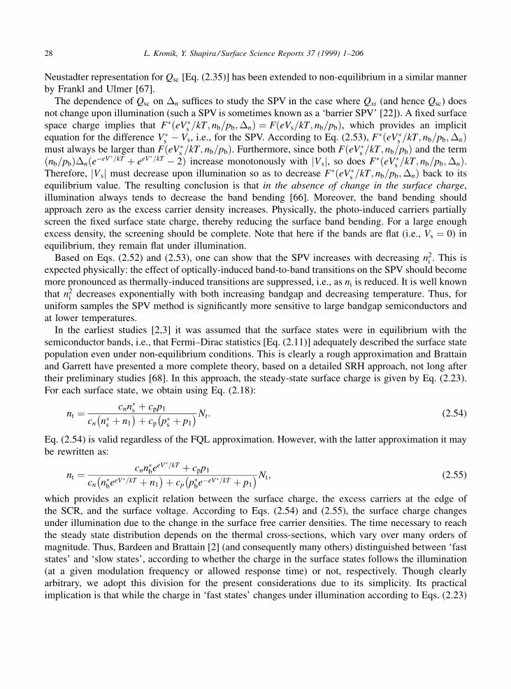
obtained from partial derivatives of Eqs. (2.52) and (2.53) for the expressions involving Qsc, and ofEqs. (2.23) and (2.55) for the expressions involving Qss. An example of such a calculation is given inFig. 11, which features the dependence of dVs=d�p
�� �� on V0s for a 1015 cmÿ3 p-InP sample with surface
states of varying density. Here, the equilibrium value of Vs is arbitrarily scanned, assuming it is set by aproper density of `slow states'.
Much physical insight may be obtained from Fig. 11. As a general trend, the SPV tends to increasewith increasing initial band bending. For small V0
s , the obtained SPV is linear in V0s . For larger V0
s theslope of the SPV versus V0
s gradually decreases. Deep into inversion or accumulation, dVs=d�p
�� ��obtains a limiting value, which is independent of the surface states. This independence is obtainedbecause for a given energy position, the states are almost `completely full' or `completely empty' if theband bending is large enough. Hence, the terms describing the variation of Qss in Eq. (2.57) arenegligible with respect to the terms describing the variation of Qsc. The limiting values of dVs=d�p
�� ��are easily shown to be �kT=e� and �kT=e��nb=pb� (for a p-type sample) for the inversion andaccumulation regimes, respectively. For reasonably doped samples, the second value is orders ofmagnitude smaller than the ®rst. Thus, the SPV measurement is, inherently, signi®cantly less sensitiveto accumulated surfaces than to depleted or inverted surfaces. Physically, in the case of accumulation,minority photocarriers are swept towards the bulk, where they may easily recombine due to theabundance of majority carriers. However, in the case of depletion or inversion, minority photocarriersare swept towards the surface, where the majority carrier density is lower and chances forrecombination are reduced. Thus, in accumulation the sample is inherently more `resistant' toillumination-induced changes in its charge distribution and only a relatively small SPV is necessary toreinstate charge neutrality.
L. Kronik, Y. Shapira / Surface Science Reports 37 (1999) 1±206 29
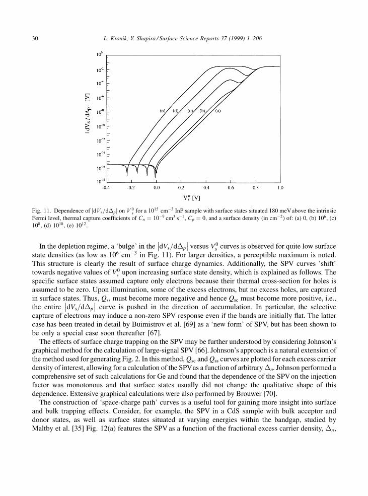
In the depletion regime, a `bulge' in the dVs=d�p
�� �� versus V0s curves is observed for quite low surface
state densities (as low as 106 cmÿ3 in Fig. 11). For larger densities, a perceptible maximum is noted.This structure is clearly the result of surface charge dynamics. Additionally, the SPV curves 'shift'towards negative values of V0
s upon increasing surface state density, which is explained as follows. Thespeci®c surface states assumed capture only electrons because their thermal cross-section for holes isassumed to be zero. Upon illumination, some of the excess electrons, but no excess holes, are capturedin surface states. Thus, Qss must become more negative and hence Qsc must become more positive, i.e.,the entire dVs=d�p
�� �� curve is pushed in the direction of accumulation. In particular, the selectivecapture of electrons may induce a non-zero SPV response even if the bands are initially ¯at. The lattercase has been treated in detail by Buimistrov et al. [69] as a `new form' of SPV, but has been shown tobe only a special case soon thereafter [67].
The effects of surface charge trapping on the SPV may be further understood by considering Johnson'sgraphical method for the calculation of large-signal SPV [66]. Johnson's approach is a natural extension ofthe method used for generating Fig. 2. In this method, Qsc and Qss curves are plotted for each excess carrierdensity of interest, allowing for a calculation of the SPVas a function of arbitrary �n. Johnson performed acomprehensive set of such calculations for Ge and found that the dependence of the SPVon the injectionfactor was monotonous and that surface states usually did not change the qualitative shape of thisdependence. Extensive graphical calculations were also performed by Brouwer [70].
The construction of `space-charge path' curves is a useful tool for gaining more insight into surfaceand bulk trapping effects. Consider, for example, the SPV in a CdS sample with bulk acceptor anddonor states, as well as surface states situated at varying energies within the bandgap, studied byMaltby et al. [35] Fig. 12(a) features the SPV as a function of the fractional excess carrier density, �n,
Fig. 11. Dependence of jdVs=d�pj on V 0s for a 1015 cmÿ3 InP sample with surface states situated 180 meV above the intrinsic
Fermi level, thermal capture coef®cients of Cn � 10ÿ9 cm3 sÿ1, Cp � 0, and a surface density (in cmÿ2) of: (a) 0, (b) 106, (c)
108, (d) 1010, (e) 1012.
30 L. Kronik, Y. Shapira / Surface Science Reports 37 (1999) 1±206
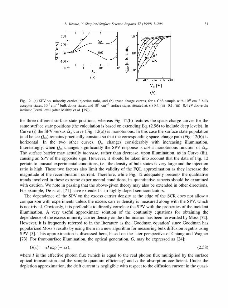
for three different surface state positions, whereas Fig. 12(b) features the space charge curves for thesame surface state positions (the calculation is based on extending Eq. (2.96) to include deep levels). InCurve (i) the SPV versus �n curve (Fig. 12(a)) is monotonous. In this case the surface state population(and hence Qsc) remains practically constant so that the corresponding space-charge path (Fig. 12(b)) ishorizontal. In the two other curves, Qss changes considerably with increasing illumination.Interestingly, when Qss changes signi®cantly the SPV response is not a monotonous function of �n.The surface barrier may actually increase, rather than decrease, upon illumination, as in Curve (iii),causing an SPV of the opposite sign. However, it should be taken into account that the data of Fig. 12pertain to unusual experimental conditions, i.e., the density of bulk states is very large and the injectionratio is high. These two factors also limit the validity of the FQL approximation as they increase themagnitude of the recombination current. Therefore, while Fig. 12 adequately presents the qualitativetrends involved in these extreme experimental conditions, its quantitative aspects should be examinedwith caution. We note in passing that the above-given theory may also be extended in other directions.For example, De et al. [71] have extended it to highly-doped semicondcutors.
The dependence of the SPV on the excess carrier density at the edge of the SCR does not allow acomparison with experiments unless the excess carrier density is measured along with the SPV, whichis not trivial. Obviously, it is preferable to directly correlate the SPV with the properties of the incidentillumination. A very useful approximate solution of the continuity equations for obtaining thedependence of the excess minority carrier density on the illumination has been forwarded by Moss [72].However, it is frequently referred to in the literature as the `Goodman equation' since Goodman haspopularized Moss's results by using them in a new algorithm for measuring bulk diffusion legnths usingSPV [5]. This approximation is discussed here, based on the later perspective of Chiang and Wagner[73]. For front-surface illumination, the optical generation, G, may be expressed as [24]:
G�x� � �I exp �ÿ�x�; (2.58)
where I is the effective photon ¯ux (which is equal to the real photon ¯ux multiplied by the surfaceoptical transmission and the sample quantum ef®ciency) and � the absorption coef®cient. Under thedepletion approximation, the drift current is negligible with respect to the diffusion current in the quasi-
Fig. 12. (a) SPV vs. minority carrier injection ratio, and (b) space charge curves, for a CdS sample with 1016 cmÿ3 bulk
acceptor states, 1012 cmÿ3 bulk donor states, and 1011 cmÿ2 surface states situated at: (i) 0.4, (ii) ±0.1, (iii) ±0.4 eV above the
intrinsic Fermi level (after Maltby et al. [35]).
L. Kronik, Y. Shapira / Surface Science Reports 37 (1999) 1±206 31

neutral region, and vice versa in the depletion region. Let us consider a speci®c case where the minoritycarriers are electrons. Based on the above approximation, using Eqs. (2.2), (2.3) and (2.58), andassuming the excitation is suf®ciently low-level so that Eq. (2.20) may be used, the continuity equationfor electrons becomes:
Dd2�n�x�
dxÿ �n�x�
�� �I exp �ÿ�x� � 0; (2.59)
where the subscript `n' has been omitted from D and � for brevity.For a thick sample, the back surface boundary condition is clearly �n�1� � 0. At the space charge
edge, the following `surface recombination type' boundary condition is used:
Dd�n�x�
dx
����x�w
� S�n�w�; (2.60)
where S is assumed constant. If one further assumes that the SCR width is much smaller than both theabsorption length and the diffusion length, i.e., w� 1=� and w� L, the excess minority carrier at theSCR edge may be expressed by the compact form:
�n�w� � �L
1� �L� 1
S� D=LI: (2:61�
S should be interpreted as an effective drift velocity for electrons reaching the SCR edge, rather thanas a true SRV. However, under the above assumptions, the effect of the SCR is negligible. Indeed,Eq. (2.61) would have the same form had w been neglected in advance and S interpreted as a `real' SRV.Under the above restrictions, �n�w�, which is proportional to I, may be inserted into Eqs. (2.53) and(2.55). Thus, the obtained SPV is explicitly expressed in terms of the incident photon ¯ux. Interestingly,no use of the majority carrier continuity equation is made in this approach. The reason is that under theassumptions of quasi-neutrality and FQL, the distribution of the majority carriers is completelyspeci®ed by that of the minority carriers. Such an approach has been used by Frankl and Ulmer [67] forobtaining explicit expressions of the small signal SPV. These expressions were further simpli®ed byLile [74] for obtaining expressions which may be compared to experiment with relative ease. Agenerally similar approach has been followed by Zuev and Litovchenko [75]. Note that under the FQLapproximation the SRV did not appear in the Poisson equation in any way. At a super®cial glance, itmay seem as if, e.g., for a constant Qss, the SRV does not affect the magnitude of the SPV. This isincorrect, because the SRV enters the equations even under this approximation through the dependenceof �n�w� on the illumination intensity. Indeed, one would physically expect a reduced SPV the largerthe SRV is since the illumination-induced deviation from equilibrium is smaller, as also veri®ednumerically [76].
We emphasize that the boundary condition of Eq. (2.60) at the edge of the SCR is only an ad hocapproximation, which stems from neither the continuity equations nor the SRH statistics. Chiang andWagner [73] suggested that a rigorous analytical approach would involve replacing the boundarycondition of Eq. (2.60) with a detailed current balance in the SCR. Such a balance would properlyaccount for generation and recombination processes inside the SCR, as well as use proper SRHstatistics instead of SRV-based approximations. This paper has fostered several generalization attemptsby other authors, discussed below.
32 L. Kronik, Y. Shapira / Surface Science Reports 37 (1999) 1±206

Choo et al. [77] presented a current balance calculation which is simpler than Chiang and Wagner's.By integrating the steady-state continuity equation across the SCR, the relation:
Jn�0� ÿ Jn�w� � JG ÿ JR; (2.62)
is obtained, where:
JG � e
Z w
0
Gn�x� dx; JR � e
Z w
0
Rn�x� dx: (2:63�
Here, Jn�0� is the surface recombination current, eRS, and Jn�w� is the diffusion current at the edge ofthe SCR, which may be expressed by �n�w� from the solution of Eq. (2.59). In principle, the chargebalance condition, Eq. (2.24), and the current balance condition, Eq. (2.62), provide two non-linearcoupled algebraic equations for the SPV and for �n�w�. Thus, under the FQL approximation, the SPVmay be found by numerically solving algebraic equations, but not differential ones. Moreover, in somecases analytical expressions can be obtained [77,78].
Having made the most out of the FQL approximation, we turn to examining the behavior of thequasi-Fermi levels more closely. A point of frequent confusion is the relation between the energyseparation of the quasi-Fermi levels at the depletion region edge, �Fn ÿ Fp�jx�w (see Fig. 10) and theSPV. Fig. 13 features a schematic band-diagram of a p±n junction under forward bias. It shows that thepotential energy drop across the SCR is equal to the energy separation between the positions of themajority carrier quasi-Fermi levels in the quasi-neutral regions [24]. If the potential drop across theSCR is not the result of electrical bias but is rather a photovoltage this equality is no longer exact. Thisis because the illumination may affect the position of the majority carrier quasi-Fermi levels in thequasi-neutral regions, due to photo-induced excess carrier generation. However, for low and moderateinjection levels, the equality is still a good and useful approximation. Chiang and Wagner [73] assumeda similar equality, SPV � Fn ÿ Fp
ÿ ���x�w
. Unfortunately, the latter relation is erroneous for the case of afree surface [77]. As opposed to the case depicted in Fig. 13, the energy separation here is not betweentwo majority carrier quasi-Fermi levels on opposite sides of the SCR, but rather between majority and
minority quasi-Fermi levels on the same side of the SCR. In order to understand more clearly why theequality is false, consider another gedanken experiment: Suppose one performs the SPV experiment onan `ideal' uniform sample which has no surface states and no bulk states whatsoever. Such a sample hasno band bending in equilibrium and no surface barrier would develop in such a case even undersigni®cant illumination. Thus, while the difference between Fn and Fp may be considerable, the SPVwould remain zero. (For completeness, one should also assume equal electron and hole mobilities sothat the Dember voltage is also zero ± see Section 2.2.4 below).
Fig. 13. Schematic diagram of quasi-Fermi levels in an illumination pÿ n junction.
L. Kronik, Y. Shapira / Surface Science Reports 37 (1999) 1±206 33

In many respects, the theory of the open-circuit photovoltage at a metal-semiconductor interface isvery similar to the free surface case since in both the SCR is completely contained in the semiconductorpart of the junction. A major difference between the two is that the metallic overlayer has a bulk Fermilevel, while the surface states do not. Consequently, the identi®cation of the SPV with the difference inmajority carrier quasi-Fermi level on the two sides of the metal-semiconductor junction is at least asgood an approximation as in the above described p±n junction. For, e.g., a p-type semiconductor, therelation:
SPV � Fn�x � 0� ÿ Fp�x � w�; (2.64)
is a good approximation, as long as there is an intimate contact between the metal and thesemiconductor [79]. If the quasi-Fermi levels are ¯at across the SCR, Eq. (2.64) is equivalent to theansatz of Chiang and Wagner and the latter is therefore a reasonable approximation for metal±semiconductor interfaces, as also con®rmed by numerical simulations [80].
Another difference between the metal±semiconductor junction and the free surface has to do with thecurrent boundary conditions. While the free surface current is of a SRH-type recombination current, themetal±semiconductor interface current is associated with thermionic emission. From thermionicemission considerations, an effective interface recombination rate in the form of Rn � vn�n andRp � vp�p is deduced [80], where vn �vp� is the effective recombination velocity for electrons (holes).This formulation is based on the combined thermionic emission-diffusion approach of Crowell and Sze[81], extended by Green and Shewchun [82] to minority carriers.
The early 1980s have seen a renewed interest in examining the validity of the FQL approximation formetal-semiconductor junctions: By assuming a recombination current which is constant across the SCRand a parabolic SCR potential, Panayotatos and Card [83] have shown that the minority carrier quasi-Fermi level may deviate considerably from the FQL approximation. Heasell [84] has shown that themajority carrier quasi-Fermi level may considerably deviate from ¯atness near the semiconductor±metal interface, in order to supply the current necessary to support the thermionic emission across theinterface. Choo [80] has shown that even if the minority carrier quasi-Fermi level is reasonably ¯atacross most of the SCR, it may undergo signi®cant variations near the SCR edge, to the point of causingorder-of-magnitude errors in current calculations.
Physically, the gradients in quasi-Fermi levels (see Fig. 10) imply net electron and hole currents: (a)towards the back part of the surface, driven by a concentration gradient caused by the non-uniformillumination, (b) towards the front surface, driven by the need to supply the surface recombination/emission current. This may also be established mathematically. By using a modi®ed form of the drift-diffusion equation and the integrated continuity equation (Eq. (2.62)), Pauwels et al. expressed thesurface current in the form: [85]:
Jn�0� � e�eff n�0� ÿ n�w� expÿeVs
kT
� �� �� e
Z w
0
Gn�x� ÿ Rn�x�� ��1�x� dx; (2.65)
where:
�eff�x� � DnR w
0exp �ÿeV�x�=kT� dx
; (2.66)
�1�x� �R w
xexp �ÿeV�x�=kT� dxR w
0exp �ÿeV�x�=kT� dx
; (2.67)
34 L. Kronik, Y. Shapira / Surface Science Reports 37 (1999) 1±206

with a similar expression for holes. The factor in the left square brackets in Eq. (2.65) is the differencebetween the real surface concentration of electrons and that predicted by the FQL approximation. Thus,veff is interpreted as an effective transport velocity across the SCR. If generation and recombination inthe SCR (and hence the integral term in Eq. (2.65)) are negligible, conservation of the FQL approxi-mation requires that veff be in®nite because a ®nite current must be sustained. However, from Eq. (2.66)it is clear that veff is ®nite. This re-establishes that with non-zero steady-state recombination currents,the FQL assumption is necessarily an approximation. 0 � �1�x� � 1 is the fraction of the net generatedelectron density (at a point x) which is transported to the front surface. A similar equation for the otheredge of the SCR, w, results in another similar fraction, 0 � �2�x� � 1, such that �1�x� � �2�x� � 1 forall x in the SCR. Thus, �2�x� is the fraction of the net generated electron density at a point x which istransported to the back of the SCR, in agreement with the physical picture given above.
Based on the foregoing analysis, De Visschere [86] has formulated a transport validity criterion forthe FQL approximation, which states that the transport should not be limited by veff, i.e., that veff mustbe larger than both the effective SRV and the diffusion velocity, vd, in the quasi-neutral region. (Thiscriterion should be added to other FQL validity criteria discussed above). The ®rst transport restriction,veff � SRV, is, in a sense, a quantitative compact criterion for the allowed magnitude of the surfacerecombination. The second, veff � �d , is usually satis®ed as a result of an earlier condition ± the SCRwidth being smaller than the diffusion length. Similar results have also been obtained by Jang using asomewhat different approach [87]. Finally, Choo has studied numerically both the free surface SPV[77] and the metal±semiconductor interface SPV [80], and concluded that typically the FQLapproximation is considerably more satisfactory in the former than in the latter.
In studies of the metal-semiconductor interface, it is evidently meaningless to equate Qsc with Qss.Instead, one uses current balance considerations. Recent studies have applied the current balanceequation (Eq. (2.62)) for both minority and majority carriers [79,80]. In such studies the Poissonequation is circumvented by assuming a potential pro®le in the SCR, usually a parabolic one. Theassumption of a parabolic potential lifts the need of using the Poisson equation just as the FQLassumption lifts the need for using the majority carrier continuity equation. As noted in Section 2.1.1,for a comprehensive solution one must determine the distribution of the potential, the electron densityand the hole density by solving the Poisson equation with the two continuity equations. Under bothassumptions, one makes an educated guess for a reasonably exact solution of one of these threeparameters, thereby eliminating one equation. No assumption is free of restrictions. Here, the parabolicpotential naturally limits the validity of the treatment to the depletion regime. Worse, under certainconditions a semiconductor in the depletion regime may invert upon illumination [77]. However, whenapplied with care the approximation may yield very good results. We also note that Dhariwal andDeoraj [79] has expressed the SPV as a function of the photocurrent density. Analogously, we haveexpressed above the SPV as a function of the injection ratio, but not of the illumination intensity.
Due to the inadequacy of the FQL approximation for some free surface SPV problems, a similartheoretical approach was adapted in the 1990s by some authors not only for metal±semiconductorstudies but also for free surface studies [33,88,89]. Konstantinov and Tsarenkov [88] assumed thatgeneration and diffusion currents dominate the minority carrier behavior and thermionic emissiondominates the majority carrier behavior. Judging by the full current balance equation (Eq. 2.62), this isclearly not a universal conclusion. Thus, while their analysis leads to very simple mathematicalexpressions, its validity is limited. Darling [33] performed a complete current balance, but assumed aconstant recombination rate throughout the SCR ± an assumption which is not always realistic. The
L. Kronik, Y. Shapira / Surface Science Reports 37 (1999) 1±206 35

recent analysis of Liu et al. [89] is the most advanced one in the sense that it makes a full currentanalysis with realistic SRH statistics. However, it is limited to the case of a negligible change in Qss.
So far, we have only discussed the case where @n=@t and @p=@t in Eq. (2.2) are both zero, usuallyknown as `dc SPV'. Use of modulated illumination was mentioned only in the context of the `fast' and`slow' surface states. However, if the modulation frequency is high enough (`ac SPV'), a steady-stateperiodic variation of n, p, and the SPV, must be taken into account. Mathematical analyses of suchsteady-state solutions usually assume that all pertinent quantities follow a `exp �i!t�' dependence,where ! is the modulation frequency. Use of this dependence in Eq. (2.2) yields @n=@t � i!n 6� 0, witha similar expression for holes. One particular consequence of this, which is important for some of theadvanced analyses reviewed in Section 5, is the modi®cation of the diffusion length [90]. If the steadystate diffusion equation (i.e., the continuity equation in the absence of electric ®eld) is solved understeady-state periodic conditions, the effective diffusion length is given by:
L�!� �����������������
D�
1� i!�
r� L�! � 0�����������������
1� i!�p : (2.68)
Analytical expressions for ac SPVs have been developed almost exclusively within the framework ofsmall SPV signals (SPV� kT=e), where the steady-state periodic SPV can be safely assumed todepend linearly on the steady-state photocurrent. The initial groundwork for such calculations was laidby Nakhmanson [91] with subsequent extensions, re®nements, and applications by Nakhmansonhimself [92] and by Munakata et al. [93±96]. According to these authors, the photocurrent density,Jph�!�, is typically extracted from a current-balance calculation. As in the case of the dc SPV, the mostsimple calculations utilize the Moss approach, i.e., use the concept of an effective, SCR-related, SRV.The photocurrent density, Jph, is then calculated from:
Jph � ÿeDnd�n�x�
dx
����x�w
� ÿeS�n�w�; (2.69)
which results in:
Jph � eI�L�!�
1� �L�!� �S
S� D=L�!� exp �i!t�; (2.70)
where L�!� is given by Eq. (2.68).Eq. (2.70) reduces to particularly simple forms if: (a) the diffusion length is relatively long, so that
the effective SRV, S, is much higher than the diffusion velocity, D=L, and (b) the absorption coef®cient,�, is much larger or much smaller than 1=L. Then:
Jph � eI�L�!� exp �i!t�; for�L� 1; (2.71a)
Jph � eI exp �i!t�; for�L� 1: (2.71b)
Once Jph�!� is determined, the SPV can be calculated using the relation [91,94]:
SPV�!� � Jph�!�Zeff�!�; (2.72)
where
Zeff�!� � 1
��1=Rj � i!Cj� �1
1=Req � i!Ceq
: (2.73)
36 L. Kronik, Y. Shapira / Surface Science Reports 37 (1999) 1±206
The effective photovoltage±photocurrent±density impedance, Zeff (with units of Ohm�area), iscomposed of parallel resistance (Rj) and capacitance (Cj) components, corresponding to thecontributions of the various SPV-in¯uencing mechanisms. These may include minority and majoritycarrier transport, depletion and inversion layers, surface states, etc. [94], and may be lumped into anequivalent resistance, Req, and capacitance, Ceq.
Expressions for the different resistance and capacitance components are obtained by appropriatemodi®cations of the derivations presented above, which take the time-dependence into account. As asimple and illustrative example, which is also used for some quantitative analyses in Section 5, weconsider the calculations of Kamieniecki [97], concentrating on an n-type material for simplicity. Thisauthor assumed a simple charge balance with negligible SCR generation/recombination, such that therate of free hole ¯ow to the semiconductor surface is equal to Jph=e. The overall increase rate of freeholes (ps) and trapped electrons (nt) at the semiconductor surface is then given by:
dps
dt� 1
eJph ÿ Rsp;
dnt
dt� Rsn ÿ Rsp; (2:74�
where Rsp (Rsn) is the surface recombination rate of holes (electrons). Using Eq. (2.74), the overallcharge neutrality can be expressed as:
ÿ dQsc
dt� dQss
dt� e
dps
dtÿ e
dnt
dt� Jph ÿ eRsn: (2.75)
Assuming a small SPV signal, we obtain:
dQsc
dt� dQsc
d�SPV� �d�SPV�
dt� ÿCsc
d�SPV�dt
; (2.76)
where Csc is the SCR capacitance. Assuming the FQL approxination and a small signal SPVapproximation and using Eq. (2.21), we obtain:
Rsn � sndns � snd nb expeV�skT
� �� �' sn
eSPV
kT
� �nb exp
eVs
kT
� �: (2:77�
Combining Eqs. (2.75)±(2.77) yields:
Cscd�SPV�
dt� Jph ÿ Csc
SPV
�s
; (2.78)
where
�s � Csc
sn�e2=kT�nb exp �eVs=kT� : (2.79)
The steady-state solution of Eq. (2.78) is:
SPV�!� � Jph
Csc=�s � i!Csc
: (2.80)
Thus, Eq. (2.80) is indeed a special case of Eq. (2.73), where Ceq � Csc and Req � �s=Csc. Physically,the equivalent capacitance here is due to the space charge region and the equivalent resistance here isrelated to the majority carrier surface recombination.
L. Kronik, Y. Shapira / Surface Science Reports 37 (1999) 1±206 37
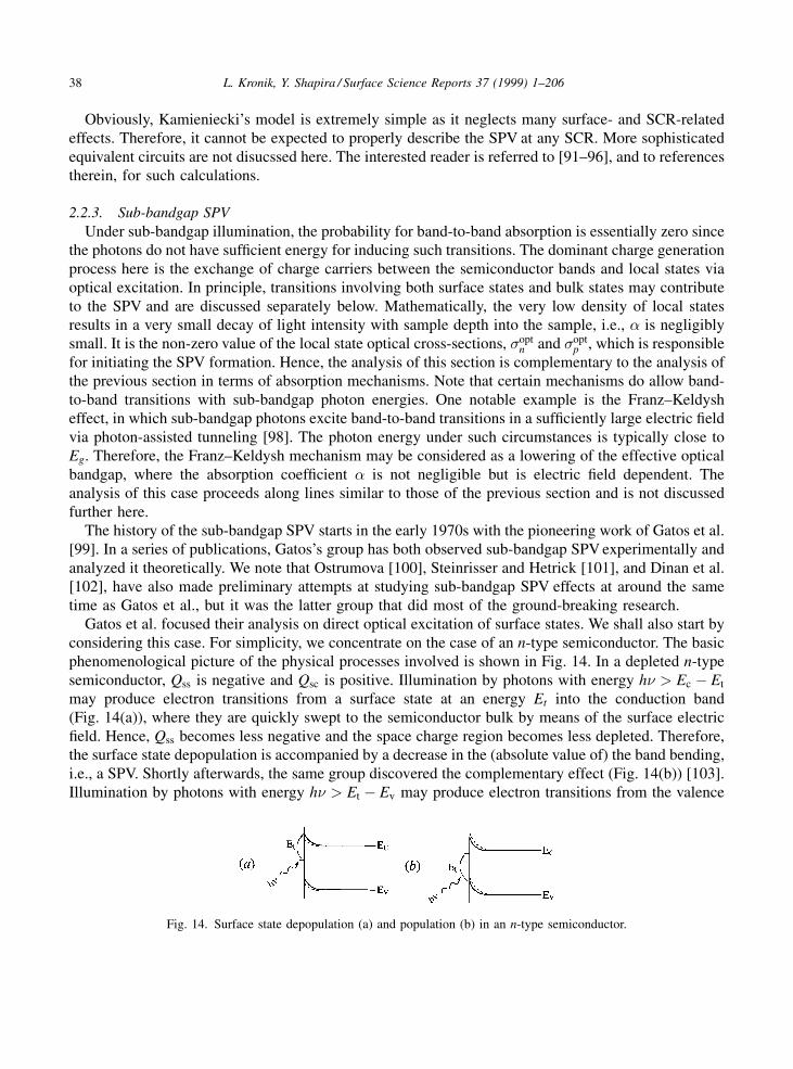
Obviously, Kamieniecki's model is extremely simple as it neglects many surface- and SCR-relatedeffects. Therefore, it cannot be expected to properly describe the SPV at any SCR. More sophisticatedequivalent circuits are not disucssed here. The interested reader is referred to [91±96], and to referencestherein, for such calculations.
2.2.3. Sub-bandgap SPV
Under sub-bandgap illumination, the probability for band-to-band absorption is essentially zero sincethe photons do not have suf®cient energy for inducing such transitions. The dominant charge generationprocess here is the exchange of charge carriers between the semiconductor bands and local states viaoptical excitation. In principle, transitions involving both surface states and bulk states may contributeto the SPV and are discussed separately below. Mathematically, the very low density of local statesresults in a very small decay of light intensity with sample depth into the sample, i.e., � is negligiblysmall. It is the non-zero value of the local state optical cross-sections, �opt
n and �optp , which is responsible
for initiating the SPV formation. Hence, the analysis of this section is complementary to the analysis ofthe previous section in terms of absorption mechanisms. Note that certain mechanisms do allow band-to-band transitions with sub-bandgap photon energies. One notable example is the Franz±Keldysheffect, in which sub-bandgap photons excite band-to-band transitions in a suf®ciently large electric ®eldvia photon-assisted tunneling [98]. The photon energy under such circumstances is typically close toEg. Therefore, the Franz±Keldysh mechanism may be considered as a lowering of the effective opticalbandgap, where the absorption coef®cient � is not negligible but is electric ®eld dependent. Theanalysis of this case proceeds along lines similar to those of the previous section and is not discussedfurther here.
The history of the sub-bandgap SPV starts in the early 1970s with the pioneering work of Gatos et al.[99]. In a series of publications, Gatos's group has both observed sub-bandgap SPV experimentally andanalyzed it theoretically. We note that Ostrumova [100], Steinrisser and Hetrick [101], and Dinan et al.[102], have also made preliminary attempts at studying sub-bandgap SPV effects at around the sametime as Gatos et al., but it was the latter group that did most of the ground-breaking research.
Gatos et al. focused their analysis on direct optical excitation of surface states. We shall also start byconsidering this case. For simplicity, we concentrate on the case of an n-type semiconductor. The basicphenomenological picture of the physical processes involved is shown in Fig. 14. In a depleted n-typesemiconductor, Qss is negative and Qsc is positive. Illumination by photons with energy h� > Ec ÿ Et
may produce electron transitions from a surface state at an energy Et into the conduction band(Fig. 14(a)), where they are quickly swept to the semiconductor bulk by means of the surface electric®eld. Hence, Qss becomes less negative and the space charge region becomes less depleted. Therefore,the surface state depopulation is accompanied by a decrease in the (absolute value of) the band bending,i.e., a SPV. Shortly afterwards, the same group discovered the complementary effect (Fig. 14(b)) [103].Illumination by photons with energy h� > Et ÿ Ev may produce electron transitions from the valence
Fig. 14. Surface state depopulation (a) and population (b) in an n-type semiconductor.
38 L. Kronik, Y. Shapira / Surface Science Reports 37 (1999) 1±206
band into a surface state situated at an energy Et above the valence band maximum, Ev (which areequivalent to hole transitions from the surface state to the valence band). Such transitions would makeQss more negative and hence the surface barrier would increase. Naturally, this requires that the surfacestate in question be not completely ®lled prior to excitation. Super-bandgap illumination typically(although not always) tends to decrease the surface barrier. Thus, this effect was ®rst dubbed`photovoltage inversion' or, when in the presence of other `regular' transitions, `photovoltagequenching' [103]. The phenomenology of this type of SPV is more complicated since the photo-generated holes tend to accumulate at the surface rather than be swept away by the electric ®eld. Thus,there is initially no charge separation and hence no SPV. For the SPV to develop it is necessary to havea signi®cant diffusion of the excess holes into the bulk and/or a signi®cant recombination of electronsand holes inside the SCR.
As in the previous section, the key to a quantitative analysis is in ®nding the surface potential forwhich charge balance is maintained under illumination. As a ®rst step, let us assume that all transitionsinvolving the minority carriers (holes, in this case) are negligible. This assumption may be valid inpractice, for example, if (a) the (®lled) state is positioned in the upper half of the bandgap and photonswith h� < Eg=2 are used, and (b) the state's thermal cross-section for holes is very small. With the helpof Eqs. (2.12)±(2.15) and Fig. 1, the rate equation for the surface charge density may be written as:
dnt
dt� ÿgth
n ÿ goptn � rth
n � ÿ�optn In�t ÿ cnn�t n1 � cn�Nt ÿ n�t �n�s : (2.81)
Speci®cally, under steady-state conditions, we obtain:
Qss � ÿen�t � ÿecnn�s Nt
�optn I � cn�n1 � n�s �
: (2.82)
The case of unipolar excitation considered here is particularly simple since the quasi-Fermi level mustbe rigorously ¯at. This is because the electron current in itself, and not just the total current as before,must vanish in steady-state. Moreover, if the surface illumination is not too strong, the excess majoritycarrier density in the bulk is negligible. Physically, this is because the illumination only `returns to thebulk' electrons caught in the surface state, but does not produce a new excess. Hence:
n�s � n�b exp ÿeV�s =kTÿ � � nb exp ÿeV�s =kT
ÿ �: (2.83)
By combining Eqs. (2.82) and (2.83), Qss is explicitly expressed in terms of the surface potential.Furthermore, Qsc is expressed by the usual relation (2.52). Therefore, the change in surface potential,i.e., the SPV, may be found. Szaro [104] has studied the theoretical SPV obtained under theseassumptions. He has found that the sub-bandgap SPV increases with increasing surface barrier, as in thecase of the super-bandgap SPV. However, as opposed to the latter case, the SPV does not change sign ator near the transition from the depletion to the accumulation regime. This is because the nature of thephysical process involved always makes the surface more positive regardless of the initial sign of thesurface band bending. Szaro has further noted that the SPV signal increases with increasing surfacestate density, decreasing bulk electron concentration, and decreasing temperature. All theseobservations are easily explained physically. The larger the surface density is, more electron transitionsare induced with the same photon ¯ux, and hence the larger the SPV is. The smaller the bulk charge is,screening of the surface disturbance from equilibrium is more dif®cult, and hence a larger SPV isneeded to change the bulk charge distribution accordingly. Finally, lowering the temperature has the
L. Kronik, Y. Shapira / Surface Science Reports 37 (1999) 1±206 39

same effect as in the super-SPV case, namely, suppressing thermally-induced transitions. For the latterreason, the sub-bandgap SPV is also expected to decrease with increasing semiconductor bandgap[6,105].
In the particularly simple case of unipolar excitation, a relatively low illumination level may result ina relatively small electron current even during the transient response. As a result, Eq. (2.83) remains areasonable approximation even under non-steady state conditions. Unlike the super-bandgap SPV case,the transient response may be treated analytically here by combining Eq. (2.81) with Eq. (2.83) and thePoisson equation [110]. Based on these equations, it is readily observed that the change in nt (and hencethe change in surface voltage) is, in general, non-exponential, because n�s depends on V�s whichobviously changes during the transient response. The transient response is approximately exponential,however, if the recombination term is negligible with respect to the generation terms in Eq. (2.81).
The optical cross-section, �optn , is photon energy dependent (just like the band-to-band absorption
coef®cient). Lucovsky [106] has quantum-mechanically calculated the theoretical dependence of �optn
on the photon energy by studying the transition from a bulk impurity level to a parabolic band assuminga delta-function potential for the impurity. His work was later generalized by Grimmeiss and Ledebo[107] for non-parabolic, non-spherical bands. These calculations show that in general:
�optn ' h�� �ÿk
h� ÿ Et� �n; (2.84)
where k is either 1 or 3 and n is either 1, 1:5, 2, 2:5, or 3, depending on the nature of the opticaltransitions and the type of the impurity center. Unfortunately, it is much more dif®cult to calculatesimilar expressions for surface states due to the reduced symmetry of the energy levels and potentialsinvolved. Nevertheless, for lack of a better model, a dependence of the type given by Eq. (2.84) is oftenused for surface states as well, with an adequate ®t between theory and experiment [108].
The case of optical interaction of the surface states with minority carriers is less amenable to simpleanalysis. While the rate equation (Eq. (2.81)) may be easily extended to account for transitionsinvolving the valence band, the quasi-Boltzmann relation (Eq. (2.83)) is not expected to hold for holes.The reason is that excess holes are generated and accumulated locally near the surface, as opposed tothe previous case where the electrons were quickly swept out of the space charge region. To the best ofour knowledge, this case has not been dealt with analytically in the literature and one must resort tonumerical analysis.
Several other complications to the simple picture may arise. If there is more than one type ofindependent surface states, a rate equation similar to Eq. (2.81) ± for interaction with one or both of thebands ± must be written for each level separately. Therefore, different surface states may`communicate' via the bands. For example, some electrons excited from a given surface state intothe conduction band may be re-trapped by a different state, thereby reducing the deviation fromequilibrium and hence the SPV [109]. If the surface state density is very high, or two surface states arederived from the same physical complex, direct optical excitation of carriers from one level to the othermay become possible. Mathematically, this would require the addition of appropriate terms to the rateequations. Another possible complication is related to the effectiveness of the `communication'between surface states and the semiconductor bulk. As noted in the previous sub-section, the timenecessary for the equilibration of the surface and the bulk may vary over many orders of magnitude andresults in the distinction between `slow' and `fast' states. A somewhat similar effect is related to therelaxation time of the sample back to its equilibrium surface voltage value following optical excitation[110,111]. If, for example, the SPV was a result of electron excitation from surface states into the bulk,
40 L. Kronik, Y. Shapira / Surface Science Reports 37 (1999) 1±206
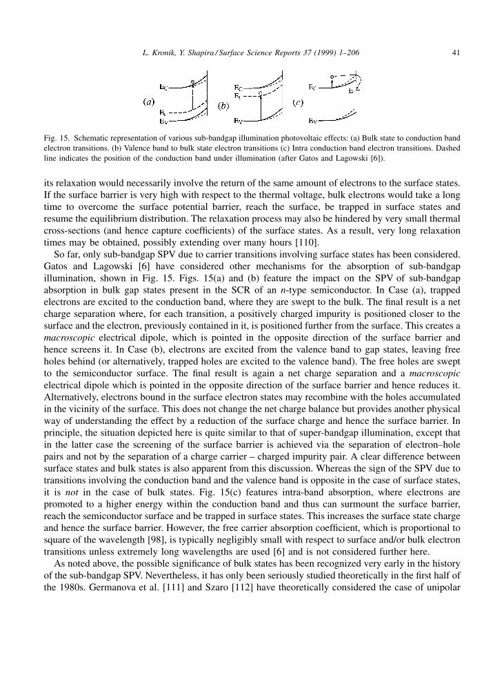
its relaxation would necessarily involve the return of the same amount of electrons to the surface states.If the surface barrier is very high with respect to the thermal voltage, bulk electrons would take a longtime to overcome the surface potential barrier, reach the surface, be trapped in surface states andresume the equilibrium distribution. The relaxation process may also be hindered by very small thermalcross-sections (and hence capture coef®cients) of the surface states. As a result, very long relaxationtimes may be obtained, possibly extending over many hours [110].
So far, only sub-bandgap SPV due to carrier transitions involving surface states has been considered.Gatos and Lagowski [6] have considered other mechanisms for the absorption of sub-bandgapillumination, shown in Fig. 15. Figs. 15(a) and (b) feature the impact on the SPV of sub-bandgapabsorption in bulk gap states present in the SCR of an n-type semiconductor. In Case (a), trappedelectrons are excited to the conduction band, where they are swept to the bulk. The ®nal result is a netcharge separation where, for each transition, a positively charged impurity is positioned closer to thesurface and the electron, previously contained in it, is positioned further from the surface. This creates amacroscopic electrical dipole, which is pointed in the opposite direction of the surface barrier andhence screens it. In Case (b), electrons are excited from the valence band to gap states, leaving freeholes behind (or alternatively, trapped holes are excited to the valence band). The free holes are sweptto the semiconductor surface. The ®nal result is again a net charge separation and a macroscopic
electrical dipole which is pointed in the opposite direction of the surface barrier and hence reduces it.Alternatively, electrons bound in the surface electron states may recombine with the holes accumulatedin the vicinity of the surface. This does not change the net charge balance but provides another physicalway of understanding the effect by a reduction of the surface charge and hence the surface barrier. Inprinciple, the situation depicted here is quite similar to that of super-bandgap illumination, except thatin the latter case the screening of the surface barrier is achieved via the separation of electron±holepairs and not by the separation of a charge carrier ± charged impurity pair. A clear difference betweensurface states and bulk states is also apparent from this discussion. Whereas the sign of the SPV due totransitions involving the conduction band and the valence band is opposite in the case of surface states,it is not in the case of bulk states. Fig. 15(c) features intra-band absorption, where electrons arepromoted to a higher energy within the conduction band and thus can surmount the surface barrier,reach the semiconductor surface and be trapped in surface states. This increases the surface state chargeand hence the surface barrier. However, the free carrier absorption coef®cient, which is proportional tosquare of the wavelength [98], is typically negligibly small with respect to surface and/or bulk electrontransitions unless extremely long wavelengths are used [6] and is not considered further here.
As noted above, the possible signi®cance of bulk states has been recognized very early in the historyof the sub-bandgap SPV. Nevertheless, it has only been seriously studied theoretically in the ®rst half ofthe 1980s. Germanova et al. [111] and Szaro [112] have theoretically considered the case of unipolar
Fig. 15. Schematic representation of various sub-bandgap illumination photovoltaic effects: (a) Bulk state to conduction band
electron transitions. (b) Valence band to bulk state electron transitions (c) Intra conduction band electron transitions. Dashed
line indicates the position of the conduction band under illumination (after Gatos and Lagowski [6]).
L. Kronik, Y. Shapira / Surface Science Reports 37 (1999) 1±206 41
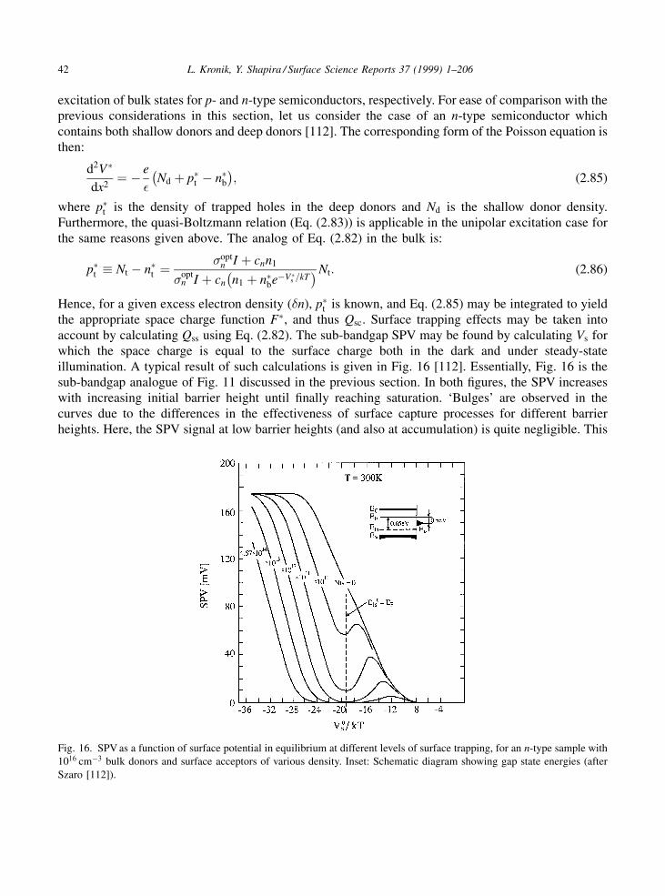
excitation of bulk states for p- and n-type semiconductors, respectively. For ease of comparison with theprevious considerations in this section, let us consider the case of an n-type semiconductor whichcontains both shallow donors and deep donors [112]. The corresponding form of the Poisson equation isthen:
d2V�
dx2� ÿ e
�Nd � p�t ÿ n�bÿ �
; (2.85)
where p�t is the density of trapped holes in the deep donors and Nd is the shallow donor density.Furthermore, the quasi-Boltzmann relation (Eq. (2.83)) is applicable in the unipolar excitation case forthe same reasons given above. The analog of Eq. (2.82) in the bulk is:
p�t � Nt ÿ n�t ��opt
n I � cnn1
�optn I � cn n1 � n�beÿV�s =kT
ÿ �Nt: (2.86)
Hence, for a given excess electron density (�n), p�t is known, and Eq. (2.85) may be integrated to yieldthe appropriate space charge function F�, and thus Qsc. Surface trapping effects may be taken intoaccount by calculating Qss using Eq. (2.82). The sub-bandgap SPV may be found by calculating Vs forwhich the space charge is equal to the surface charge both in the dark and under steady-stateillumination. A typical result of such calculations is given in Fig. 16 [112]. Essentially, Fig. 16 is thesub-bandgap analogue of Fig. 11 discussed in the previous section. In both ®gures, the SPV increaseswith increasing initial barrier height until ®nally reaching saturation. `Bulges' are observed in thecurves due to the differences in the effectiveness of surface capture processes for different barrierheights. Here, the SPV signal at low barrier heights (and also at accumulation) is quite negligible. This
Fig. 16. SPV as a function of surface potential in equilibrium at different levels of surface trapping, for an n-type sample with
1016 cmÿ3 bulk donors and surface acceptors of various density. Inset: Schematic diagram showing gap state energies (after
Szaro [112]).
42 L. Kronik, Y. Shapira / Surface Science Reports 37 (1999) 1±206

is because the sub-bandgap SPV response is smaller due to the smaller number of bulk states withrespect to the band density of states. The saturation in the SPV with increasing barrier height is due toan additional mechanism. As the barrier height increases, some of the bulk states in the vicinity of thesurface may be shifted above the Fermi level. Such states are essentially empty and do not contribute tooptical absorption. Thus, as the barrier height is increased, there are more bulk states in the surfaceSCR, but the number of those participating in the SPV generation remains constant beyond a certainbarrier height.
Performing a similar analysis, Germanova et al. [111] have noticed that in certain situations a bulkstate involving majority carriers may actually increase the surface barrier rather than decrease it.Consider, for example, an n-type semiconductor with a depletion-type surface barrier. As explainedabove, electrons excited from bulk states into the conduction band should decrease the surfacepotential. However, the increase of the free electron density also enhances the probability for electroncapture in surface states and hence increases the surface state occupation. Evidently, making the surfacemore negative in an n-type semiconductor should increase the surface barrier.
In order to consider the speci®c results of Germanova et al. [111], we note they have been obtainedfor a p-type semiconductor, i.e., holes are excited from deep bulk states to the valence band, wherebysome of them are trapped in donor-like surface states. Fig. 17(a) features the dependence of the SPV onthe bulk state density obtained by Germanova et al. For relatively large bulk densities, the SPV isnegative, i.e., the ( p-type) surface barrier is decreased, as is the normal case. For decreased bulk statedensities the SPV is inverted, i.e., the surface trapping effect is dominant and the surface barrierincreases. This behavior may be further understood with the help of Fig. 17(b), which shows thecorresponding space-charge curves for high and low bulk state densities. In the high bulk state densitycase, the surface states are essentially ®lled with holes even before illumination (which means that allsurface donors are ionized). Hence, the capture of holes under illumination is negligible, Qss does notchange appreciably under illumination, and the increase in Qsc decreases the band bending, just like in
Fig. 17. (a) SPV vs. bulk state density, and (b) space charge curves in the dark (solid lines) and under equilibrium (dashed
lines) for a bulk state density of 1:5 � 1014 cmÿ3 (A) and 1:1 � 1018 cmÿ3 (B), in a p-type sample with 5 � 1011 cmÿ2 surface
states. l ÿ low illumination intensity, h ± high illumination intensity (after Germanova et al. [111]).
L. Kronik, Y. Shapira / Surface Science Reports 37 (1999) 1±206 43
the super-bandgap SPV case. However, in the low bulk state density case, the surface states aresigni®cantly populated by electrons under equilibrium. Hence, a substantial increase in Qss is observedunder illumination. Since the increase of Qsc upon illumination in this case is relatively slight, the netresult is an increase in the surface barrier. Such a SPV inversion mechanism has been observedexperimentally (see Section 4.2 below) as well as re-con®rmed theoretically by Davydov et al. [113].
Szaro [114] has also studied the case of an n-type semiconductor with a deep donor-like bulk stateunder bipolar sub-bandgap excitation. There, electrons may overall be excited from the valence band tothe conduction band, via the intermediate gap state, and the problem is quite similar to that of super-bandgap SPV. Therefore, the SPV problem may be solved analytically as in Section 2.2.2. Szaroperformed such calculations while varying the ratio between surface state electron and hole capturecoef®cients. He noted that hole trapping in acceptor-like surface states greatly increases the SPV byreducing the surface charge. This is also feasible with super-bandgap illumination, but here surfaceeffects are much more pronounced with respect to free carrier screening effects. Finally, Szaro notedthat if the bulk state density were relatively small, its effect on the Poisson equation would benegligible, and the excess free carrier densities in the bulk would become independent of the bulk statedensity. Thus, it may seem as if for low bulk state densities the SPV is independent of this density. Theonly difference (analysed in a subsequent publication [115]) is that the lower the bulk state density thelonger is the transient response. This conclusion may seem quite strange as one expects that the morebulk states there are, the more ef®cient the optical generation is and the larger is the deviation fromequilibrium (and hence SPV). Szaro's analysis was performed assuming that those bulk states providedthe sole recombination mechanism and not only the sole generation mechanism. Under such conditions,the excess carrier density is really independent of bulk state density since the reduced generation iscompensated by reduced recombination. However, in the presence of a competing recombinationmechanism (e.g., via other defect states or via band-to-band recombination), these conclusions are nolonger valid.
Several of the studies surveyed above [111,114] suggest that bulk state effects on the SPV arerelatively weak with respect to surface state effects. The relative importance of surface and bulktransitions has been examined by Leibovitch et al. [116]. By performing two integrations of the Poissonequation and using integration by parts, one may recast the Poisson equation in the one-dimensionalintegral form:
Vs � ÿZ w
0
x��x��
dx; (2.87)
which facilitates a direct relation between the charge density in the SCR and the surface potential.Moreover, the charge balance condition may be written in the form:
Qss � ÿQsc � ÿZ w
0
��x� dx: (2.88)
Let us consider the case of small perturbations, which is more readily amenable to analyticalprocedures. For small signals, the variation in the surface potential may be related to the variation in thecharge density by performing calculus of variations, while taking into account that w is also dependenton the perturbation. This yields:
�Vs � w
��Qss �
Z w
0
�wÿ x����x��
dx: (2.89)
44 L. Kronik, Y. Shapira / Surface Science Reports 37 (1999) 1±206
For an order of magnitude estimate, let us assume that ���x� is constant throughout the SCR.Furthermore, we de®ne the effective surface density of the variation in bulk state volume density as�Qb � w � ��. Assuming that �Qb and �Qss are equal, integrating Eq. (2.89) directly yields that theSPV due to the surface perturbation is really larger, but only by a factor of two. Thus, SPS isindeed inherently more sensitive to surface states than to bulk states, but not by much. (This iscompatible with the linguistic observation that `surface' pertains to the `photovoltage' rather than to the`spectroscopy'). A larger difference between surface and bulk state excitation on the SPV arisesin detailed calculations. This is because for, e.g., w � 0:1 mm, a reasonable surface state density of1011 cmÿ2 is equivalent to a bulk volume density of 1016 cmÿ3, which is a relatively high value forsamples of reasonable quality.
2.2.4. The Dember potential
In the two preceding sections, we have consistently assumed that the SPV stems only from changesin the surface potential drop across the SCR. In this sub-section, we examine the validity of thisassumption by studying the voltage which may form across the region of the sample which iselectrically neutral in equilibrium, known as the Dember photovoltage [25,61]. Consider a samplewhich has no surface states and hence no surface SCR and no SCR-related SPV. The physics ofthe Dember photovoltage has to do with non-uniform generation or recombination in a sample.For example, under super-bandgap illumination through the top surface of the sample, the gene-ration decays into the sample due to optical absorption [see Eq. (2.58)]. The ensuing gradient inexcess carrier concentration results in the diffusion of both electrons and holes further into thesemiconductor bulk. The electrons are more mobile than holes and hence diffuse faster into the bulk.This creates a net electric ®eld in the direction of the bulk, which drives the holes deeper into thesample and retards the motion of the electrons into the sample. Even though the sample is entirelyneutral in the dark, it is no longer so under illumination. The sign of the Dember photovoltage isdetermined solely by the sign of the faster diffusing species and hence it is positive for both n-type andp-type semiconductors.
The steady-state illumination-induced electric ®eld across the sample may be calculated from therequirement of zero total current, Jn � Jp � 0. Expressing the currents by the drift-diffusionexpressions (Eq. (2.3)) and assuming quasi-neutrality, i.e.,
�n�x� � ���x�; d�n�x�dx
� d�p�x�dx
; (2.90)
it is easy to show that the electric ®eld is given by [90]:
E�x� � �Dp ÿ Dn��d�n�x�=dx��0 � q��n � �p��n�x� ; (2.91)
where �0 � e�nb�n � pb�p� is the dark conductivity of the sample. It should be noted that the quasi-equilibrium conditions (Eq. (2.90)) are clearly an approximation because a non-zero net charge mustexist in the presence of a non-zero electric ®eld. However, the electric ®eld as given by Eq. (2.91) maybe used in Poisson's equation to calculate the net difference �pÿ �n and thus estimate the errorinvolved [117]. For, e.g., extrinsic silicon, the quasi-neutrality assumption is good for any injectionlevel [90]. Since under the above assumptions the surface voltage is zero in equilibrium, the SPV isimmediately calculated by integrating Eq. (2.91). Using the semi-in®nity boundary condition (i.e., no
L. Kronik, Y. Shapira / Surface Science Reports 37 (1999) 1±206 45

excess carriers at the back side) and the Einstein relations (Eq. (2.6)), we obtain [118]:
SPV � ÿZ 1
0
E�x� dx � kT
e
�n ÿ �p
�n � �p
ln 1� e��n � �p��n�0��0
� �: (2.92)
Relation (2.92) describes the dependence of the Dember photovoltage on the excess carrier density atthe front end of the nominally quasi-neutral region. The Dember photovoltage vanishes when �n � �p
since no net separation of charge and hence no electric ®eld are to be expected when both chargespecies are equally mobile. In addition, it is clear that the Dember effect is more pronounced inmaterials where the mobility difference between electrons and holes is fairly large. The Dember effectis typically signi®cant only under high injection conditions where �n�0� is of the order of nb (seeEq. (2.92)). For example, for n-type GaAs at �n=nb � 10ÿ2 one obtains that the SPV is only � 5 mV.The number is even smaller for, e.g., silicon, where the ratio of electron to hole mobility is smaller.However, since the magnitude of the Dember potential increases logarithmically with excess carrierdensity, it is not always negligible at higher illumination intensities.
The Dember photovoltage is related to electron and hole diffusion coupled by means of the electric®eld in the quasi-neutral region. Therefore, in order to determine �n�0� the ambipolar transportequation [90] which properly describes such coupled transport should be used. (The ambipolartransport equation is obtained from inserting the drift-diffusion current expressions (Eq. (2.3)) in thecontinuity equations (Eq. (2.2)). The resulting equations are linearly combined so as to nullify the termcontaining the derivative of the electric ®eld.) Assuming the electron and hole generation andrecombination rates are equal, the result is:
�aE�x� d�n�x�dx
� Da
d2�n�x�dx2
� G�x� ÿ R�x� � 0; (2.93)
where �a and Da are the ambipolar mobility and diffusion coef®cient, respectively, given by:
�a � �nÿ p��n�p
n�n � p�p
; Da � �n� p�DnDp
nDn � pDp
: (2.94)
Eq. (2.93) implies that in the presence of a coupling electric ®eld, the effective mobility and diffusioncoef®cient of the charge carriers are modi®ed to account for the coupling effect to the other chargecarrier type. Even if a standard SRV type boundary condition (see Eq. (2.60)) is taken at the surface(x � 0), Eq. (2.93) cannot usually be analytically solved. This is because of the electric ®eld term whichcouples it to the Poisson equation. An analytical solution can be obtained if �a � 0, i.e., n � p. This is areasonable approximation only if the sample is close to intrinsic or the injection is extremely high.
A few more comments are in order. So far we have only discussed the case where the bands are ¯at inthe dark and no surface states are present. Then, the Dember effect is the sole cause of the SPV. In thegeneral case, it is usually assumed that the overall SPV is the sum of the SCR-related SPV and theDember photovoltage, where each is calculated separately. However, the two potentials are inter-related: Under signi®cant Dember effect conditions, the minority carrier transport equation (Eq. (2.59))has to be replaced by the ambipolar transport equation (Eq. (2.93)). In addition, the boundary conditionfor the Dember potential should either be taken as an effective SRV at the edge of the SCR (Eq. (2.60)),or be replaced with the detailed current balance equation (Eq. (2.62)). This coupling alters the precisevalue of the SPV due to each mechanism with respect to its value in the absence of the othermechanism. However, it does not modify the physical picture given above.
46 L. Kronik, Y. Shapira / Surface Science Reports 37 (1999) 1±206
While the `classical' Dember photovoltage discussed above is due to non-uniform generation, non-uniform recombination also results in a photovoltage `of the same genre as the Dember voltage' [119].For example, Buimistrov et al. [69] have discussed the presence of a signi®cant bulk state density whichcauses a signi®cant difference between electron and hole capture as a source of SPV. If the generation isfairly uniform (as in, e.g., sub-bandgap illumination) and there is a signi®cant surface recombination,electrons and holes will diffuse in the direction of the surface and the Dember voltage would benegative, rather than positive. Interestingly, a sub-bandgap photovoltage signal which has beenobserved as early as 1965(!) by Nadzhakov and Balabanov [120], was intepreted in terms of such arecombination-related Dember effect rather than in terms of defect state transitions, as in Section 2.2.3.While Nadzhakov and Balabanov offered no proof for this mechanism in their speci®c case, its possiblecontribution in other cases is almost always overlooked.
2.2.5. Effect of buried interfaces
All of the preceding discussion has been devoted solely to a study of semi-in®nite, uniform bulksamples. However, actual semiconductor samples may be thin, i.e., not much larger than the diffusionlength and/or the absorption length, so that excess carriers may be present near their back part as well.Samples may also comprise of a multi-layer structure, which has several buried interfaces due tohomojunctions and heterojunctions in the structure.
At a ®rst glance, interfaces which are buried deep enough into the sample may seem unable tocontribute to the measured SPV signal, due to screening by a thick enough quasi-neutral region.However, this statement is erroneous. To understand why, let us consider a semiconductor samplecomprising a semiconducting ®lm grown on a semiconducting bulk substrate, which may have differentmaterial parameters. A schematic typical band-lineup of such a structure in the dark (solid curve) andunder illumination (dashed curve) is shown in Fig. 18 [20]. There are two SCRs in such a sample (notincluding the back contact, assumed to be Ohmic): an interface one (between the substrate and the ®lm)and a surface one (between the ®lm and the ambient). Fig. 18 clearly shows that optical absorption inany non-neutral region present within the sample (be it band-to-band or defect state to band) maycontribute to the measured SPV signal because the potential of the free surface is linked to any otherilluminated region, no matter how deep within the sample, as the energy bands are serially connected.Moreover, Dember effects may arise from any illuminated quasi-neutral region of the sample. Thus, thesensitivity of SPV measurements to a certain region in the semiconductor is limited only by theabsorption length of the photons, i.e., by the possibility of introducing an excess of free carriers in theregion of interest.
The sensitivity of SPV measurements to buried interfaces is underscored by the two different SPVscenarios shown in Fig. 18. In both, the SPV is produced by changes in the band-bending of both theinterface and the surface SCRs. However, in one case the surface related SPV dominates, whereas in theother case the interface-related SPV dominates. At a second glance, the sensitivity to buried interfacesshould not be too surprising: In a normal photodiode, the potential difference between the two contactschanges even though the photovoltaically active region may be very far from the contacts. The sameoccurs here, except that one `contact' is free.
While the above arguments are simple, they have been frequently overlooked in the past. As a result,relatively little experimental or theoretical work has been devoted to studying the in¯uence of buriedinterfaces on the SPV. The theory of junction-related surface photovoltage is given in detail elsewhere[25,59], as noted in Section 2.2.1. Thus, it is worthwhile to elaborate on it here only to the extent that
L. Kronik, Y. Shapira / Surface Science Reports 37 (1999) 1±206 47
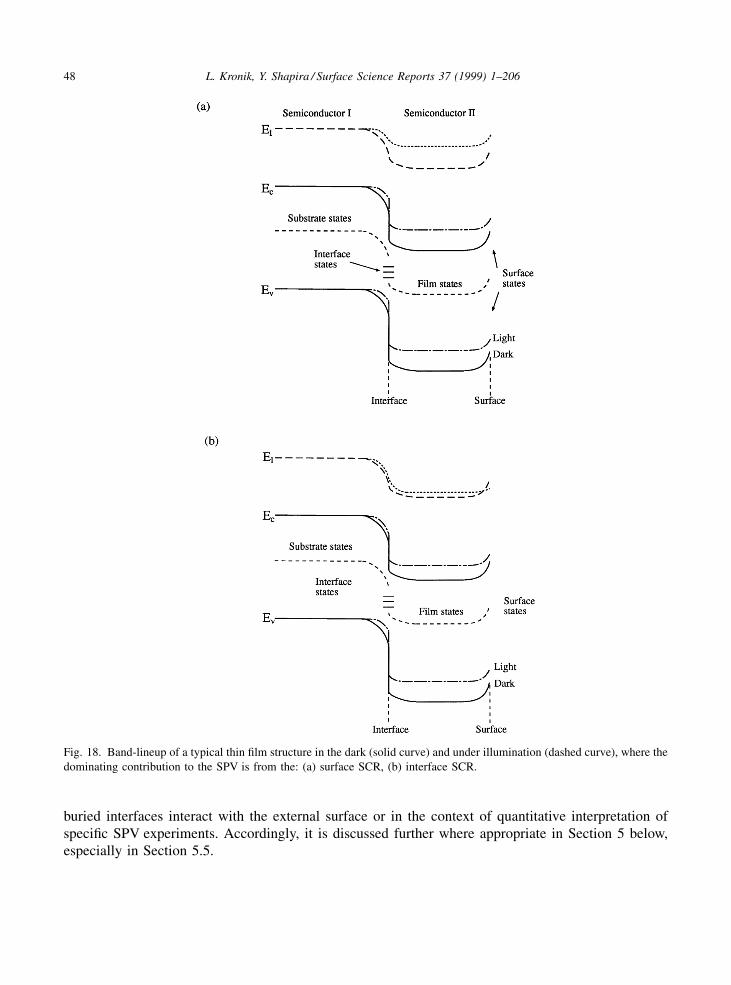
buried interfaces interact with the external surface or in the context of quantitative interpretation ofspeci®c SPV experiments. Accordingly, it is discussed further where appropriate in Section 5 below,especially in Section 5.5.
Fig. 18. Band-lineup of a typical thin ®lm structure in the dark (solid curve) and under illumination (dashed curve), where the
dominating contribution to the SPV is from the: (a) surface SCR, (b) interface SCR.
48 L. Kronik, Y. Shapira / Surface Science Reports 37 (1999) 1±206
To conclude this section, we note that in SPV the experimentally measured quantity is strictly asurface quantity and as a result the technique is highly surface-sensitive. However, it is by no meanssensitive only to the surface. Rather, it is sensitive to the entire surface SCR (via super- or sub-bandgapabsorption), to the quasi-neutral bulk (via the Dember effect) and even to buried interfaces locatedanywhere within the sample (as long as they can be reached by photons). Therefore, by proper designand interpretation of experiments the SPV may be effectively used to gain information about varioussemiconductor interface and bulk properties, in addition to semiconductor surface properties.
3. Experimental methods
SPV measurements are non-trivial because the surface potential is a built-in potential, rather than anexternal potential. In other words, the surface potential is not equal to the difference in Fermi levelsbetween the front and back surfaces. Therefore, it cannot be measured simply with some form ofvoltmeter. Moreover, in the case of a free surface, the application of any contact for indirect electricalmeasurements of the built-in voltage (e.g., current±voltage or capacitance±voltage analyses) willinvariably alter the surface properties and hence the quantity under measurement. Consequently, manyelaborate techniques for measuring the surface potential (or at least changes of it) without applying adirect electrical contact have emerged. This chapter is dedicated to a discussion of these methods.
3.1. The Kelvin probe
3.1.1. Principles of operation
An important key to several SPV measurement techniques may be found by re-examining theelectronic band structure at a semiconductor surface. By using Fig. 4, as well as Eq. (2.36), weconclude that any change in the surface potential, eVs, causes a change of equal magnitude in thesurface work function, Ws. Therefore, in the absence of photochemical activity, the change in surfacework function is equal to the SPV (in absolute value terms).
One of the oldest techniques for determining relative changes in work functions is measuring thework function difference between two materials forming the two sides of a parallel plate capacitor. Aschematic band diagram of two metals in such an arrangement (®rst employed by Kohlrausch [121]) isshown in Fig. 19. Prior to connection (Fig. 19(a)) the metals are electrically neutral, no macroscopicelectrical ®elds arise, and the two metals share the same local vacuum level. Upon short-circuiting themetals (Fig. 19(b)) charge must ¯ow from the metal with smaller work function to the metal with largerwork function until equilibration of the Fermi levels is achieved. As in any parallel plate capacitor, thischarge transfer results in an electric ®eld in the gap between the two plates and a drop in the localvacuum level across this gap. Using Fig. 19(b) we conclude that this potential energy drop is equal tothe difference in the work functions of the two metals. The corresponding potential drop is usuallyknown as the contact potential difference (CPD) [22,24], i.e., eVCPD � W1 ÿW2.
As opposed to a `textbook' parallel plate capacitor, the potential drop described here is built-in and isachieved under zero bias conditions. Theoretically, if both the stored charge, Q, and the overallcapacitance, C0, are known, the CPD may be easily calculated, because Q � C0VCPD. However, theprecise measurement of the stored charge is non-trivial. This obstacle has been overcome by LordKelvin [122], who suggested that the CPD may be measured directly by a null-method. When an
L. Kronik, Y. Shapira / Surface Science Reports 37 (1999) 1±206 49

external dc bias, equal and opposite to the CPD, is applied to the capacitor (Fig. 19(c)), the Fermi levelson both metals differ by VCPD, just as in the isolated case (Fig. 19(a)). No charge exchange between themetals need take place and the capacitor is discharged. Hence, in order to determine the CPD, it suf®cesto determine the applied bias which discharges the capacitor, even if neither capacitor charge norcapacitance are known. If the spacing between the two plates is varied while the plates remainconnected under bias, the resulting capacitance change should induce a change in the capacitor chargeand hence a current in the external circuit. This current can be zero if and only if the capacitor isdischarged. Thus, the CPD may be easily found by determining the external bias for which no externalcurrents are observed upon changing the spacing between the plates. This type of arrangement is knownas the Kelvin probe arrangement, after its inventor.
The Kelvin probe arrangement has been extensively applied to the measurement of illumination-induced changes in work function starting from the earliest experiments of Bardeen and Brattain [2],and ever since. This has been achieved by Ohmically contacting the back side of the semiconductorsample to a metallic reference electrode. Since the work function of the metallic electrode does notchange under illumination the relation:
ÿe�SPV � �Ws � e�VCPD; (3.1)
is assumed, based on Eq. (2.36). It is worthwhile to closely inspect the validity of relation (3.1) for ametal±semiconductor Kelvin probe arrangement. The main cause for concern is shown in the schematicband diagram of this arrangement, given in Fig. 20. In the isolated semiconductor (Fig. 20(a)) thesurface band bending is determined by the free surface charge neutrality condition, Qss � Qsc � 0. Asthe metal is connected to the back side of the semiconductor (Fig. 20(b)) a MIS structure is formed.Thus, the band bending in the semiconductor, and hence its work function, may change. As explainedin Section 2.1.5, the appropriate charge neutrality condition becomes Qm � Qss � Qsc � 0, where theeffect of Qm may be signi®cant if the width of the capacitor gap is not much larger than the width of the
Fig. 19. Schematic band diagram of a parallel plate capacitor formed from two different metals, with the two plates:
(a) isolated, (b) short-circuited, (c) connected through a DC bias equal and opposite to the contact potential difference.
50 L. Kronik, Y. Shapira / Surface Science Reports 37 (1999) 1±206
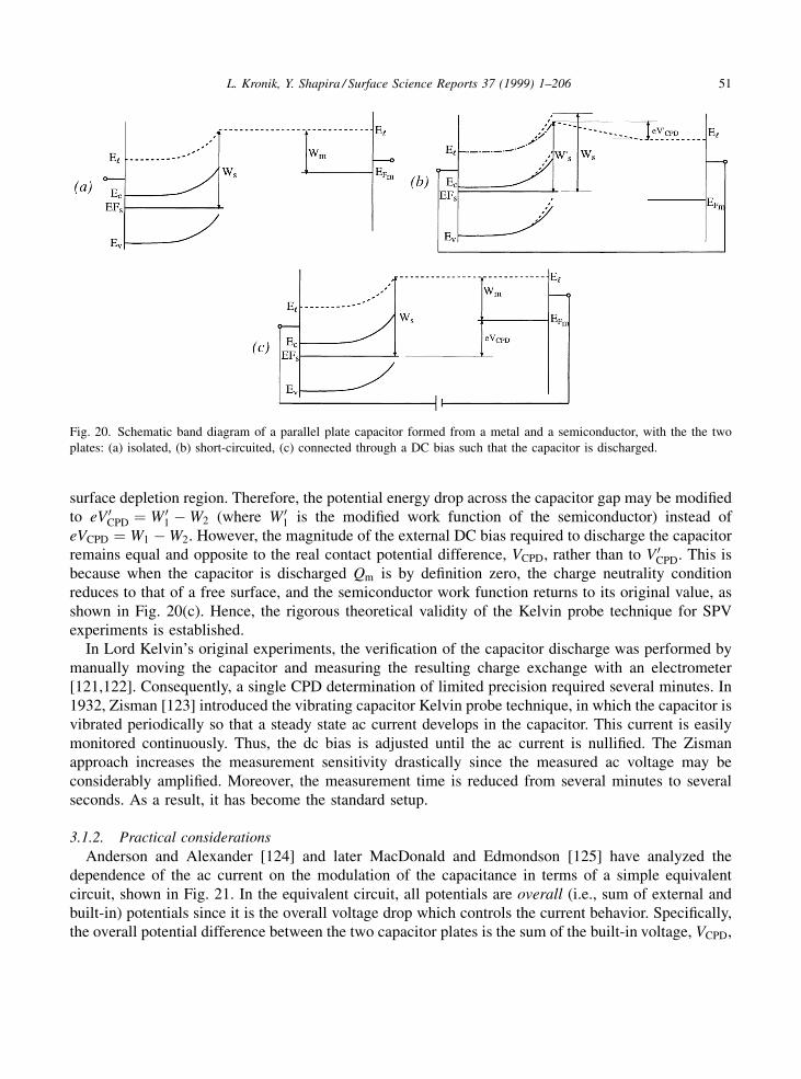
surface depletion region. Therefore, the potential energy drop across the capacitor gap may be modi®edto eV 0CPD � W 01 ÿW2 (where W 01 is the modi®ed work function of the semiconductor) instead ofeVCPD � W1 ÿW2. However, the magnitude of the external DC bias required to discharge the capacitorremains equal and opposite to the real contact potential difference, VCPD, rather than to V 0CPD. This isbecause when the capacitor is discharged Qm is by de®nition zero, the charge neutrality conditionreduces to that of a free surface, and the semiconductor work function returns to its original value, asshown in Fig. 20(c). Hence, the rigorous theoretical validity of the Kelvin probe technique for SPVexperiments is established.
In Lord Kelvin's original experiments, the veri®cation of the capacitor discharge was performed bymanually moving the capacitor and measuring the resulting charge exchange with an electrometer[121,122]. Consequently, a single CPD determination of limited precision required several minutes. In1932, Zisman [123] introduced the vibrating capacitor Kelvin probe technique, in which the capacitor isvibrated periodically so that a steady state ac current develops in the capacitor. This current is easilymonitored continuously. Thus, the dc bias is adjusted until the ac current is nulli®ed. The Zismanapproach increases the measurement sensitivity drastically since the measured ac voltage may beconsiderably ampli®ed. Moreover, the measurement time is reduced from several minutes to severalseconds. As a result, it has become the standard setup.
3.1.2. Practical considerations
Anderson and Alexander [124] and later MacDonald and Edmondson [125] have analyzed thedependence of the ac current on the modulation of the capacitance in terms of a simple equivalentcircuit, shown in Fig. 21. In the equivalent circuit, all potentials are overall (i.e., sum of external andbuilt-in) potentials since it is the overall voltage drop which controls the current behavior. Speci®cally,the overall potential difference between the two capacitor plates is the sum of the built-in voltage, VCPD,
Fig. 20. Schematic band diagram of a parallel plate capacitor formed from a metal and a semiconductor, with the the two
plates: (a) isolated, (b) short-circuited, (c) connected through a DC bias such that the capacitor is discharged.
L. Kronik, Y. Shapira / Surface Science Reports 37 (1999) 1±206 51

and the external potential difference (manifested as an energy difference between the position of theFermi levels on both sides of the capacitor). The latter is the sum of the applied bias, Vb, and the voltagedrop across the resistor R. Hence, the equivalent circuit is very similar to the real circuit except that thebuilt-in potential, VCPD, is represented as a battery which is in series with the variable external dc bias,Vb. Using the equivalent circuit, a simple use of Kirchoff's laws yields an equation for the charge on thecapacitor, Q�t�:
dQ�t�dt� Q�t�
RC�t� �VCPD � Vb
R; (3.2)
with the current obviously being the time derivative of the charge:
i � d
dtC�t�Vc�t�� �; (3.3)
where Vc�t� is the overall voltage on the capacitor.Naturally, the ac current increases with increasing ac capacitance. Therefore, it increases with
increasing probe area, increasing amplitude of vibrations, and decreasing probe-to-plate distance.However, increasing the probe area decreases the spatial resolution. Decreasing the sample-to-probedistance introduces mechanical dif®culties and increases the risk of landing the sample with the probe.In addition, mechanical instabilities, which change the sample-to-probe distance, become moreimportant since they constitute a larger fraction of the overall distance. Let us consider some typicalvalues for the parameters at hand: For a probe area of 0.5 cm2 and a probe-plate average distance of 0.5mm, C0 is less than 1 pF. With typical CPDs amounting to several volts at most, the ac current isexpected to be in the pA range at most. If one wishes to measure CPD changes down to the mV level,for example, the currents may be as small as several fA. The easiest way to read such minute currents isto use a very large value for the resistor R. For example, R � 1 G yields voltages of the order of mV tomV. It is usually convenient to construct a circuit such that the large input resistance of a voltageampli®er serves as the resistor R. Since the late 1970s, following Bonnet et al. [126], it has becomeincreasingly popular to use a low input impedance current ampli®er (i.e., a current to voltage converter).While theoretically equivalent, current detection has several practical advantages over voltagedetection, which are discussed below. If a current ampli®er is used, Eq. (3.3) is further simpli®ed to:
i � VCPD � Vb� � dC
dt: (3.4)
Eq. (3.4) is strictly valid only when the input resistance of the current ampli®er, R, is zero, but is areasonable approximation as long as R is negligible with respect to the impedance of the capacitor at
Fig. 21. Equivalent circuit diagram for the vibrating Kelvin probe arrangement.
52 L. Kronik, Y. Shapira / Surface Science Reports 37 (1999) 1±206

the vibration frequency. Unfortunately, Eq. (3.4) is frequently used in the literature for analyzing thevoltage ampli®er con®guration, for which it is clearly inappropriate.
Eq. (3.2) is a time-varying ®rst order differential equation. As such, its solution is not expected togenerally be sinusoidal even if the capacitance modulation is sinusoidal [125], unless R is negligible.Moreover, usually it is the distance between the capacitor plates rather than the capacitance itself,which is modulated sinusoidally, i.e., C�t� � C0=�1� m sin �!t��, where ! is the vibration frequencyand m is the modulation index. A practical criterion for nullifying the current, regardless of its exactmathematical form, is to establish the nullifying of the fundamental harmonic only. Typically, thefundamental harmonic is isolated in two stages, shown in Fig. 22(a). First, the ac voltage (or current) isampli®ed in a (voltage- or current-sensitive) pre-ampli®er with a band pass ®lter centered at thefundamental frequency. This greatly reduces higher harmonic contributions as well as noise at otherfrequencies [127]. Next, the fundamental frequency is ampli®ed selectively using a lock-in ampli®er.The ®nal output is a dc voltage which may be measured using any simple voltage meter and which isnulli®ed when Vb � ÿVCPD, as appropriate.
Coupling to modern automatic data acquisition systems is done by using well known negativefeedback techniques, ®rst applied to CPD measurements by Simon [128] following the work ofPalevsky et al. [129]. The desired automatic readout of VCPD may be obtained by applying the obtaineddc output (in reverse polarity) back to the vibrating capacitor circuit, as shown in Fig. 22(b). In order tounderstand why this yields the desired result, consider the formulation of the feedback circuit in termsof an equivalent feedback loop, shown in Fig. 22(c). The charge on the capacitor is determined by theeffective potential difference, VCPD � Vb. For VCPD � Vb 6� 0, an ac voltage develops on the capacitor,and is ampli®ed by means of the pre-ampli®er and the lock-in ampli®er, resulting in the dc output, Vdc.We de®ne the effective gain, G, as the ratio of the dc output to the effective potential differenceinput, i.e., G � Vdc=�VCPD � Vb�. In the feedback scheme of Fig. 22(b), Vdc � ÿVb. Therefore, weobtain the relation:
G � Vdc
VCPD ÿ Vdc
) Vdc � G
1� GVCPD: (3.5)
Fig. 22. Schematic block diagram of a Kelvin probe electrical circuit: (a) Manual mode. (b) Automatic mode. (c) Equivalent
feedback loop.
L. Kronik, Y. Shapira / Surface Science Reports 37 (1999) 1±206 53
If G is made large enough, Vdc approaches VCPD and may be monitored continuously, as in Fig. 22(b)(assuming, of course, that the time interval between two consecutive measurement points is larger thanthe electronic settling time of the circuit).
For successful Kelvin probe measurements of semiconductors, a reasonable back Ohmic contactmust be present for proper ¯ow of ac current between the capacitor plates. The resistance of this Ohmiccontact can be rather large without disturbing the measurements due to the large impedance typicallypresent anyway between the two capacitor plates. The measurement of semi-insulating samples isproblematic both because a good Ohmic contact is dif®cult to make and because the insulation of thesample mount must be extremely high or the signal is lost through leakage [130]. Furthermore, for asemi-insulating sample the voltage at the free surface of the sample may be different than the voltageapplied to the sample electrode due to the potential drop across the sample itself [131]. Finally, highresistance samples are vulnerable to stray charges and to spurious dielectric response to stray electric®elds [132]. Thus, while the measurement of high resistance samples is not impossible [130,131], itrequires extreme caution.
It is also necessary to consider the means by which a sustained and stable periodic vibration of theprobe plate is obtained. Early rudimentary mechanical designs [123,133±135] have not deliveredsuf®cient performance on either count. Therefore, they were gradually replaced by electromechanicalmethods ± typically attaching the probe plate to a moving coil or to the ¯exible diaphragm of aloudspeaker [136±138], or employing electromagnetic drivers [139±141]. Both the former [142] andthe latter [143] approaches are still employed in modern day high performance Kelvin probes.However, it is the piezoelectric drive technique, ®rst suggested by Besocke and Berger [144], which iscurrently most commonly used. In this approach, the vibrating electrode is mounted on an oscillatorreed, which is fastened at the other end to a piezoelectric ceramic. This results in a simple and easy tohandle probe, which provides stable vibrations simply by applying an appropriate ac voltage to thepiezoelectric element. Furthermore, the probe-to-sample distance may be ®ne tuned by dc biasing thepiezoelectric element. More recently, it has been shown that a bimorphous piezoelectric element mayincrease the immunity of the probe to mechanical noises and provide an even more stable operation[145].
For completeness, we note that electrode vibration has also been obtained by utilizing the ac electricforce present between capacitor plates under ac voltage [146±148]. While the performance of thisapproach (known as electrostatic excitation) is similar to that obtained using other means, it is morecomplicated and has not found widespread use, except in the Kelvin probe force microscope, discussedin detail in Section 3.4.1 below.
Being a purely electrical measurement, the Kelvin probe approach should, in principle, provideaccurate CPD readings under any ambient. Nevertheless, most surface physics experiments requireUHV conditions for obtaining a well de®ned surface for a reasonable amount of time. For suchexperiments, the Kelvin probe itself, as well as any auxiliary mechanical and electrical parts introducedinto the vacuum chamber, should be vacuum compatible. High-vacuum-compatible Kelvin probes havebeen demonstrated in the 1950s [141,149], and many UHV compatible probes have been demonstratedsince ([142±144, 150±152] are a few examples).
Despite the evident success in constructing and operating Kelvin probes in vacuum, the presence ofcontinuously moving parts in vacuo does present (surmountable) design challenges and is thus notparticularly welcome by vacuum engineers. As shall be seen below, it may also introduce problematicmechanical noises. Consequently, two alternative approaches have emerged. Delchar et al. [153] used a
54 L. Kronik, Y. Shapira / Surface Science Reports 37 (1999) 1±206

static capacitor approach. In this approach, the charge ¯ow which occurs upon CPD changes is detectedand a potential which nulls the charge ¯ow is applied within a time which is much smaller than thecapacitor discharge time constant. Anderson and Alexander [124] have suggested a double-capacitorapproach: A static capacitor which is inside the vacuum chamber is serially connected to a vibratingcapacitor which is outside the vacuum chamber. Thus, the equivalent series capacitance is modulatedand an ac current is produced without motion in the vacuum chamber. Although both techniques areelegant, they suffer from serious disadvantages. The static capacitor approach does not employsynchronous detection and hence results in a reduced signal to noise ratio (SNR). Furthermore, spuriouscurrents may be misinterpreted as CPD changes. In the double capacitor approach, the equivalentcapacitance is smaller than that obtained from a single capacitor unless the static capacitor is muchlarger than the dynamic one. However, this is hard to achieve since we have already noted that theKelvin probe capacitance is rather small to begin with. Hence, the resulting ac current is diminished andthe SNR is reduced. Bodrova et al. [154] seem to be the only ones to have actually employed such anarrangement and have reported a factor of 6 reduction in the SNR with respect to a single vibratingcapacitor arrangement. Both the static capacitor and the double capacitor approach can only detectCPD changes and not absolute CPD values. The former because it is only sensitive to changes in thecharging of the capacitor [155] and the latter because it cannot take into account the CPD between thestatic and the dynamic capacitor plates [156]. However, for SPV measurements this suf®ces.
An implicit assumption in CPD measurements is that the work function of the reference electroderemains constant during the measurement. However, the work function may be very sensitive tovariations in the ambient and thus invalidate the measurement. It is common practice to use an inertreference surface, typically gold or tin oxide [156]. Both materials maintain their work function over arelatively large range of pressures and temperatures. Tungsten is eminently suitable as a referenceelectrode material in vacuum but is very sensitive to adsorption-related changes in work function [156].More recently, a probe head made of aluminized mylar with holes allowing the continuous ¯ow ofpurge gas has been suggested for maintaining a constant reference work function in air and/or under apartial pressure of adsorbates [157]. With proper design, successful CPD measurements have beendemonstrated even under extreme conditions. These include a ¯ow reactor with temperatures as high as750 K and partial pressures of H2, O2, and CO [158], or a furnace for redox processes with temperaturesup to 1000�C and partial pressures of oxygen [159]. If the constancy of the reference work function isunder any doubt, it is always a good practice to examine it by taking a CPD measurement with respectto a well-de®ned auxiliary surface [156].
Many studies compare the work function of the sample before and after various treatments, e.g.,overlayer deposition. To that end, various mechanical arrangements where the probe may be movedaway from the sample for the duration of the treatment are usually used [130,141,149,160]. Duringsuch sample treatments, the reference electrode must be adequately protected so that its work functiondoes not change. A recent example is a Kelvin probe arrangement, which is compatible with a plasmaenhanced chemical vapor deposition process [161]. In this arrangement, the Kelvin probe is repeatedlymoved between a vacuum chamber, when the plasma is on, and a deposition chamber, when the plasmais off. Following each measurement, the stability of the Kelvin probe work function is checked against agold reference present in the vacuum chamber.
If in situ measurements are to be pursued, two conditions must be ful®lled. The ®rst condition,discussed above, is that the work function of the reference electrode does not change due to the process.The second condition is that the Kelvin probe must not interfere with the studied process. An obvious
L. Kronik, Y. Shapira / Surface Science Reports 37 (1999) 1±206 55
example is that during SPV experiments, the Kelvin probe must be semi-transparent, i.e., made of ametallic grid or a transparent conductor. A less obvious example is that during adsorption studies, theprobe may act as a shield hindering the impinging gas molecules from hitting the area below the probe[162]. Consequently, a grid structure is to be preferred for such studies. Another con®gurationsometimes used for in-situ studies is that of the rotational Kelvin probe [120,163±165]. In thisarrangement, the capacitance modulation is achieved by rotating one of the capacitor plates withrespect to the other one so that a current pulse is obtained each time the moving electrode passes overthe stationary one. Other variations on this idea include moving the Kelvin probe in parallel to thesample [166,167] or in a diagonal mode [167], or swinging the moving electrode in a pendulum motionabove the sample [168]. The moving probe may be positioned so that it does not obstruct the samplesigni®cantly and thus measurements may be performed during, e.g., adsorption [166], particle beambombardment [168], or evaporation [169,170] experiments. Another advantage of this approach is thatif several samples are positioned along the track of the moving electrode they may be measuredsimultaneously [163,170]. The `penalty' of simultaneous measurements, however, is that becausecurrent pulses have to be detected, a larger bandwidth of frequencies needs to be followed and hencethe SNR is reduced.
So far, only CPD measurements of solids has been described. However, CPD measurements ofliquids or objects immersed in liquids have also been performed from the earliest days of the Kelvinprobe [136±138]. The CPD between two liquids may also be measured by means of rotating a metallicauxiliary electrode above two juxtaposed liquid electrodes [171]. Some pitfalls have to be avoidedwhen attempting such measurements. When (at least) one electrode is liquid, an obvious problem is thenecessity to contact the liquid. Moreover, the vibration of the Kelvin probe may disturb the surface ofthe liquid and disrupt the measurement [171]. The relatively high vapor pressure of liquids makes acontamination of the probe electrode more likely, even in a gas ambient, and thus the stability of itswork function needs to be particularly examined [157]. Finally, accidental dunking of the probe head inthe solution may ruin it. Therefore, use of a disposable probe head for such measurements has beensuggested [157].
An interesting application of measuring the CPD of a liquid is that the liquid provides a clean,reproducible, and easy to obtain reference surface in a gas ambient. This is because a newuncontaminated surface can be exposed simply by pouring out some liquid [157]. Moreover, the workfunction can be calibrated using absolute half cell potential data [172]. CPD measurements whereboth electrodes are solid but one or both of them are immersed in a liquid [127,173,174] are alsoof importance since the humid environment may be crucial for accurately reproducing the requiredchemical state of the surface. While properly designed and interpreted experiments may produce awealth of important information, several pitfalls must be recognized and avoided in order to completesuch measurements successfully. Viscous damping and wave propagation in the liquid call for a lowfrequency of vibration [127]. The vibration of the reference electrode may cause a change in theCPD between supposedly stable electrodes due to the disruption of a structure in the liquid, e.g.,a ®lm of unsaturated hydrocarbon present at the surface of a metal electrode in the case of unsaturatedorganic liquids [173]. Severe problems may ensue if the liquid is partially conducting. The currentbetween the electrodes causes the apparent CPD value to approach the value of the bias betweenthe electrodes, the alternating current may be very high even in the null position, and the sensitivityof the electrodes to stray electric ®elds increases. All three effects have been observed whenCPD measurements at a polar liquid ambient were attempted [173]. Moreover, unless proper
56 L. Kronik, Y. Shapira / Surface Science Reports 37 (1999) 1±206
insulation is provided, the liquid may short circuit the sample surface to the sample holder. Finally, adifferent dif®culty may occur if one electrode is immersed in a thick solution. The work function at theelectrolyte/ambient interface may differ from that at the sample surface due to potential drops acrossthe solution [174].
3.1.3. Limitations and solutions
In this section, we describe the general factors which limit the sensitivity and accuracy of Kelvinprobe measurements. We also propose practical solutions which make it possible to minimize orcircumvent these limitations.
As in any electronic measurement, the ultimate resolution with which the CPD may be resolved isdetermined by the noise spectrum of the measurement. A comprehensive treatment of this noisespectrum was provided by Baikie et al. [175]. Many of the noise sources may be signi®cantly reducedby judicious use of electrostatic shielding. However, total shielding is extremely dif®cult, especially inthe presence of additional electrical connections [175]. Strong magnets should not be placed inproximity to the Kelvin electrodes either [156]. Much of the noise spectrum is effectively eliminated byusing a narrow-band lock-in ampli®er, where the lock-in frequency is not a multiple of a frequency withsigni®cant noise components.
The most problematic noise sources are those with a frequency equal to the vibration frequency sincethey are not eliminated by the lock-in ampli®er. One source for such signals is the residual electrostaticpick-up by the Kelvin capacitor and/or (internal and external) connecting cables. Probe driver designshave been offered, which reduce this noise by removing the driver as much as possible from thevibrating capacitor [157,175]. However, many practical designs are subject to geometrical, ease ofhandling, or other limitations which preclude such arrangements. A particularly problematic type ofdriver frequency noise is contributed by microphonics, which is a general name for ac electrical signalsproduced as a result of the vibration of conductors and insulators [176]. Since a maximal ac current isobtained when the ac capacitance is maximal, the modulation index should be large. However, anincreased amplitude of vibrations increases the microphonic effects as well [177]. Thus, a signi®canteffort has been devoted to eliminating any sources of mechanical vibrations [130,133,141,175,178±180]. Noise contributions at the driver frequency may be modeled as parasitic ac current and voltagesources, which are connected in parallel and in series, respectively, to the vibrating capacitor [176].These prevent the ac current from being perfectly nulli®ed and produce a systematic error in the CPDreading. Worse, the relative magnitude of the error term with respect to the real one, and therefore theCPD reading, may become spacing dependent [176].
A different and major cause for inaccuracy in CPD readings is stray capacitance. The two Kelvinprobe plates are also capacitively coupled to, e.g., the electrostatic shield, the walls of the vacuumchamber, and any other metallic or dielectric object [181], including sample areas of different workfunction which are not situated directly under the probe [182], and supports and connecting wires [177].If there is an appreciable CPD and/or applied bias between the electrode connected to the ampli®er andthe stray capacitance sources, the current-nullifying bias may differ from the real CPD.
Fig. 23 features a very simple equivalent circuit for analyzing stray capacitance effects. The Kelvinelectrodes are designated as `1' and `2', where `1' is the electrode connected to the ampli®er, and allstray capacitance is lumped into a single stray electrode `s' with an effective external bias, Vst. Thenullifying bias Vb may be applied to Electrode `2' or `1', as in Figs. 23(a) and (b), respectively. Forsimplicity, we assume a current ampli®er. Using Eq. (3.4), the total ac current sensed by the ampli®er in
L. Kronik, Y. Shapira / Surface Science Reports 37 (1999) 1±206 57
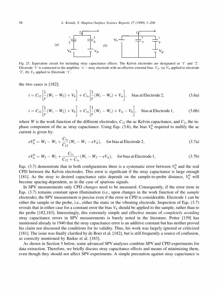
the two cases is [182]:
i � C121
e�W1 ÿW2� � Vb
� �� C1s
1
e�W1 ÿWs� � Vst
� �; bias at Electrode 2; (3.6a)
i � C121
e�W1 ÿW2� � Vb
� �� C1s
1
e�W1 ÿWs� � Vst ÿ Vb
� �; bias at Electrode 1; (3.6b)
where W is the work function of the different electrodes, C12 the ac Kelvin capacitance, and C1s the in-phase component of the ac stray capacitance. Using Eqs. (3.6), the bias V0
b required to nullify the accurrent is given by:
eV0b � W2 ÿW1 � C1s
C12
�Ws ÿW1 ÿ eVst�; for bias at Electrode 2; (3.7a)
eV0b � W2 ÿW1 � C1s
C12 � C1s
�Ws ÿW2 ÿ eVst�; for bias at Electrode 1; (3.7b)
Eqs. (3.7) demonstrate that in both con®gurations there is a systematic error between V0b and the real
CPD between the Kelvin electrodes. This error is signi®cant if the stray capacitance is large enough[181]. As the stray to desired capacitance ratio depends on the sample-to-probe distance, V0
b willbecome spacing-dependent, as in the case of spurious signals.
In SPV measurements only CPD changes need to be measured. Consequently, if the error term inEqs. (3.7) remains constant upon illumination (i.e., upon changes in the work function of the sampleelectrode), the SPV measurement is precise even if the error in CPD is considerable. Electrode 1 can beeither the sample or the probe, i.e., either the static or the vibrating electrode. Inspection of Eqs. (3.7)reveals that in either case for a constant error the bias Vb should be applied to the sample, rather than tothe probe [182,183]. Interestingly, this extremely simple and effective means of completely avoiding
stray capacitance errors in SPV measurements is barely noted in the literature. Potter [139] hasmentioned already in 1940 that the stray capacitance error is an additive constant but has neither provedhis claim nor discussed the conditions for its validity. Thus, his work was largely ignored or criticized[181]. The issue was ®nally clari®ed by de Boer et al. [182], but is still frequently a source of confusion,as correctly mentioned by Baikie et al. [183].
As shown in Section 5 below, some advanced SPV analyses combine SPV and CPD experiments fordata extraction. Therefore, we brie¯y discuss stray capacitance effects and means of minimizing them,even though they should not affect SPV experiments. A simple precaution against stray capacitance is
Fig. 23. Equivalent circuit for including stray capacitance effects. The Kelvin electrodes are designated as `1' and `2'.
Electrode `1' is connected to the ampli®er. `s' ± stray electrode with an effective external bias. Vst. (a) Vb applied to electrode
`2', (b) Vb applied to Electrode `1'.
58 L. Kronik, Y. Shapira / Surface Science Reports 37 (1999) 1±206
keeping the sample-to-probe distance, d, constant. Then, the relative difference between CPDmeasurements of different samples is minimized [130,184]. This may be impractical at liquid surfaces[157] or in the presence of thermal expansion and/or applied stress effects. Actively controlling d with afeedback loop offers a more reliable solution [142,185]. If this is not possible, it may be better to selecta spacing in which the slope of the dependence of V0
b on d is minimal, so that the error in CPD is closeto a constant [179]. Connecting the ampli®er to the static electrode [181] (i.e., to the sample rather thanto the probe) may reduce the CPD error by an order of magnitude [183]. This is because it minimizesthe stray capacities which oscillate at the same frequency as the Kelvin probe and produce stray signalswhich are picked up by the lock-in ampli®er [141]. Unfortunately, this may interfere with otherelectrical connections [184,186].
Many stray capacities may be eliminated with an electrostatic shield [149]. The stray capacitance ofthe shield itself is eliminated if the shield and probe are made of the same material [160] or if anauxilliary shield bias is used [139,181]. Many different shield designs have been proposed (see, e.g.,[131,150,176,179,184,188,189]).
Further complications arise at samples with a non-uniform work function. In an ideal parallel-platecapacitor, the measured CPD is an area weighted mean work function of the surface underneath theprobe, as long as `patches' of different work function are small with respect to d [187]. In practice,fringing effects cause the probe to sense its surroundings as well [182,183]. The relative weight of thearea underneath the probe with respect to the bordering areas depends on d and is another cause forspacing-dependent CPD readings [177].
An excellent tool for assessing stray capacities is studying the dependence of V0b on d. For samples
with uniform work function, the real Kelvin signal must dominate for d ! 0, so that the CPD error at agiven distance can be assessed [128,181,182]. For samples with a non-uniform work function, this isvalid only if V0
b is `¯at' over a range which extends from a value of d which is much smaller than allother characteristic lengths of the system [177,182]. Studying the dependence of V0
b on the amplitudeof vibrations allows for a distinction between stray capacitance amd microphonic effects. This isbecause an increased accuracy with increasing amplitude of vibrations is indicative of a straycapacitance, while the opposite is true for microphonics. Indeed, a decreased accuracy in CPD readingwith increased amplitude of vibrations has been misinterpreted for an increase in stray capacitance[181] when in fact it was due to microphonics [177]. Changing bias polarity and/or the phase betweenreference and signal in the lock-in ampli®er may also provide a key for detecting systematic CPD errors[127].
We now turn to considering how the measurement sensitivity and accuracy may be increased usingelectronic methods. We have noted above that a signi®cant modulation of the capacitance is usuallydesirable because it increases the overall current and hence the overall sensitivity of the measurement.However, this increases the harmonic distortion [125]. For a large enough modulation index, the secondharmonic may be larger than the fundamental one and further increases in the modulation indexactually reduce the signal at the fundamental harmonic. At very high frequencies, the harmonicdistortion becomes negligible. This is because for !� 1=RC0, the capacitor cannot change its chargeappreciably within a vibration period and therefore the potential on the capacitor varies as 1=C and ispurely sinusoidal [124,125]. Practically, a high enough frequency is often dif®cult to obtain because ofmechanical limitations and noise problems.
A large value of the resistor R is preferable for both minimizing harmonic distortions andmaximizing the measured ac signal. However, a large resistor R is also a source of many dif®culties.
L. Kronik, Y. Shapira / Surface Science Reports 37 (1999) 1±206 59
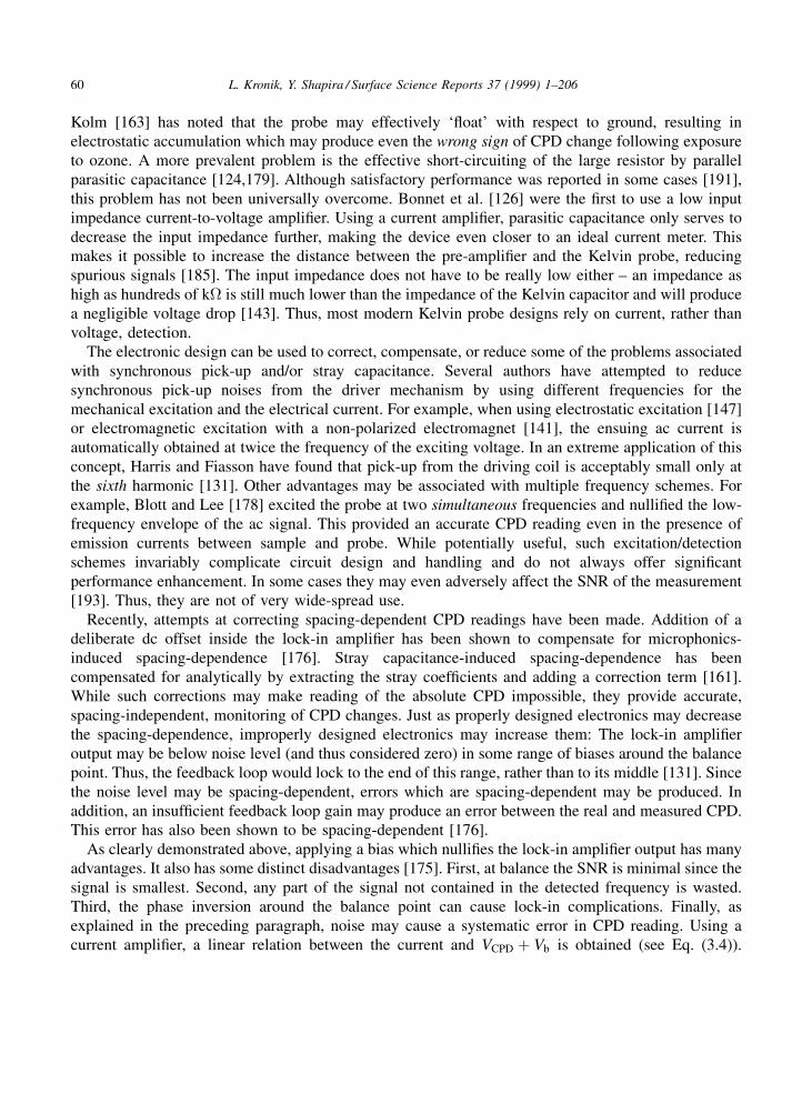
Kolm [163] has noted that the probe may effectively `¯oat' with respect to ground, resulting inelectrostatic accumulation which may produce even the wrong sign of CPD change following exposureto ozone. A more prevalent problem is the effective short-circuiting of the large resistor by parallelparasitic capacitance [124,179]. Although satisfactory performance was reported in some cases [191],this problem has not been universally overcome. Bonnet et al. [126] were the ®rst to use a low inputimpedance current-to-voltage ampli®er. Using a current ampli®er, parasitic capacitance only serves todecrease the input impedance further, making the device even closer to an ideal current meter. Thismakes it possible to increase the distance between the pre-ampli®er and the Kelvin probe, reducingspurious signals [185]. The input impedance does not have to be really low either ± an impedance ashigh as hundreds of k is still much lower than the impedance of the Kelvin capacitor and will producea negligible voltage drop [143]. Thus, most modern Kelvin probe designs rely on current, rather thanvoltage, detection.
The electronic design can be used to correct, compensate, or reduce some of the problems associatedwith synchronous pick-up and/or stray capacitance. Several authors have attempted to reducesynchronous pick-up noises from the driver mechanism by using different frequencies for themechanical excitation and the electrical current. For example, when using electrostatic excitation [147]or electromagnetic excitation with a non-polarized electromagnet [141], the ensuing ac current isautomatically obtained at twice the frequency of the exciting voltage. In an extreme application of thisconcept, Harris and Fiasson have found that pick-up from the driving coil is acceptably small only atthe sixth harmonic [131]. Other advantages may be associated with multiple frequency schemes. Forexample, Blott and Lee [178] excited the probe at two simultaneous frequencies and nulli®ed the low-frequency envelope of the ac signal. This provided an accurate CPD reading even in the presence ofemission currents between sample and probe. While potentially useful, such excitation/detectionschemes invariably complicate circuit design and handling and do not always offer signi®cantperformance enhancement. In some cases they may even adversely affect the SNR of the measurement[193]. Thus, they are not of very wide-spread use.
Recently, attempts at correcting spacing-dependent CPD readings have been made. Addition of adeliberate dc offset inside the lock-in ampli®er has been shown to compensate for microphonics-induced spacing-dependence [176]. Stray capacitance-induced spacing-dependence has beencompensated for analytically by extracting the stray coef®cients and adding a correction term [161].While such corrections may make reading of the absolute CPD impossible, they provide accurate,spacing-independent, monitoring of CPD changes. Just as properly designed electronics may decreasethe spacing-dependence, improperly designed electronics may increase them: The lock-in ampli®eroutput may be below noise level (and thus considered zero) in some range of biases around the balancepoint. Thus, the feedback loop would lock to the end of this range, rather than to its middle [131]. Sincethe noise level may be spacing-dependent, errors which are spacing-dependent may be produced. Inaddition, an insuf®cient feedback loop gain may produce an error between the real and measured CPD.This error has also been shown to be spacing-dependent [176].
As clearly demonstrated above, applying a bias which nulli®es the lock-in ampli®er output has manyadvantages. It also has some distinct disadvantages [175]. First, at balance the SNR is minimal since thesignal is smallest. Second, any part of the signal not contained in the detected frequency is wasted.Third, the phase inversion around the balance point can cause lock-in complications. Finally, asexplained in the preceding paragraph, noise may cause a systematic error in CPD reading. Using acurrent ampli®er, a linear relation between the current and VCPD � Vb is obtained (see Eq. (3.4)).
60 L. Kronik, Y. Shapira / Surface Science Reports 37 (1999) 1±206
Hence, by performing off-null measurements, i.e., measuring the current for many biases around thebias point, the latter may be found using linear regression with signi®cant gains in the SNR [194]. Thismay be rather easily performed automatically using appropriate software [142,195]. Moreover, theaverage of the signal obtained at symmetric biases around the balance points should ideally be null andhence produces the noise contribution only. This contribution may be dynamically subtracted toincrease the SNR [175]. A dif®culty, related with off-null measurements and not taken into account inthe literature, is that if the probe-to-sample distance is of the order of the depletion region width, thein¯uence of the probe on the work function (see Fig. 20) may be considerable. Then, off-nullmeasurements may exhibit a deviation from the linearity of the ac current on VCPD � Vb and may berendered invalid. A different approach was used by Baczynski [196], who analyzed the signal in thetime domain. While more complicated, his approach makes it possible to eliminate stray signals bymeans of detecting the phase difference between them and the desired signal.
The voltage resolution with which the balance point is determined is ultimately governed by eitherthe minimal noise level [191,194] or the minimal offset current [179,197] of the electronics. It is almostinvariably between �0:1 and �10 mV, depending on the probe size and distance from the sample andon the sophistication of the electronics. It is very important to distinguish between the accuracy, withwhich the balance point (i.e., the apparent CPD) is read, and the accuracy of the real CPD reading[177,183]. The latter is subject to various systematic errors, discussed above. Using suf®cientprecautions on both measurement and ambient stability, an accuracy which is better than several tens ofmV may be achieved. The error with which the SPV may be determined is much closer to the accuracyof V0
b . This is because the SPV is usually not (or almost not) subject to systematic errors, being adifference between two CPD values in a given con®guration. Consequently, SPV values may routinelybe read with mV precision.
A signi®cant disadvantage of Kelvin probe measurements is that their temporal resolution is poor.The dominant time constant is typically associated with the lock-in ampli®er. It is of the order of atleast tens of msec to several seconds, with the SNR decreasing the shorter the response time is, due tothe gain-bandwidth product rule. For example, decreasing the frequency band allowed into the lock-inampli®er requires a larger settling time and makes the measurement susceptible to instabilities inoscillation frequency [127]. The time constant increases even more if off-null measurements areemployed [195]. Using the static capacitor approach [153], a time constant of 120 ms has been achieved[198]. This value is still rather high for some applications but is extremely low for Kelvin probemeasurements. Therefore, it is clear that the Kelvin probe is ill-suited for measurements of the ac SPV.
3.1.4. Scanning Kelvin probes
A Kelvin probe may also be employed in a scanning mode: if the probe is scanned across the sample,lateral variation mapping of the CPD (and hence also SPV) may be obtained. This concept was ®rstemployed by Parker and Warren [180], who studied lateral variations in work functions of gold andgraphite with a resolution of several mm. Since then, many authors have built and successfully usedscanning Kelvin probes with lateral resolutions of several tenths of a mm to several mm (see, e.g.,[150,181,185,188,191,197,199±201]).
Butz and Wagner [202] used a 6 mm wire as the vibrating probe. Thus, they have sacri®ced lateralresolution at one axis and obtained an effective resolution of �50 mm with a voltage resolution of �20mV at the other axis. With more advanced designs, probe resolutions of several tens of mm on both axeshas been achieved [174,203,204]. MaÈckel et al. constructed a scanning Kelvin probe which features a
L. Kronik, Y. Shapira / Surface Science Reports 37 (1999) 1±206 61
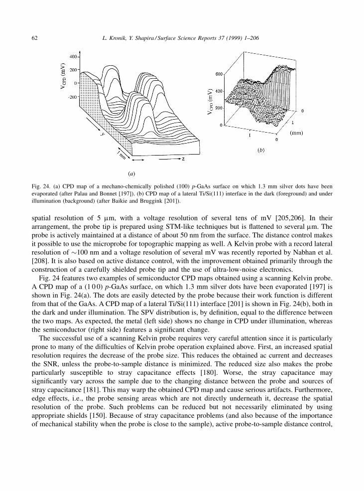
spatial resolution of 5 mm, with a voltage resolution of several tens of mV [205,206]. In theirarrangement, the probe tip is prepared using STM-like techniques but is ¯attened to several mm. Theprobe is actively maintained at a distance of about 50 nm from the surface. The distance control makesit possible to use the microprobe for topographic mapping as well. A Kelvin probe with a record lateralresolution of �100 nm and a voltage resolution of several mV was recently reported by Nabhan et al.[208]. It is also based on active distance control, with the improvement obtained primarily through theconstruction of a carefully shielded probe tip and the use of ultra-low-noise electronics.
Fig. 24 features two examples of semiconductor CPD maps obtained using a scanning Kelvin probe.A CPD map of a (1 0 0) p-GaAs surface, on which 1.3 mm silver dots have been evaporated [197] isshown in Fig. 24(a). The dots are easily detected by the probe because their work function is differentfrom that of the GaAs. A CPD map of a lateral Ti/Si(111) interface [201] is shown in Fig. 24(b), both inthe dark and under illumination. The SPV distribution is, by de®nition, equal to the difference betweenthe two maps. As expected, the metal (left side) shows no change in CPD under illumination, whereasthe semiconductor (right side) features a signi®cant change.
The successful use of a scanning Kelvin probe requires very careful attention since it is particularlyprone to many of the dif®culties of Kelvin probe operation explained above. First, an increased spatialresolution requires the decrease of the probe size. This reduces the obtained ac current and decreasesthe SNR, unless the probe-to-sample distance is minimized. The reduced size also makes the probeparticularly susceptible to stray capacitance effects [180]. Worse, the stray capacitance maysigni®cantly vary across the sample due to the changing distance between the probe and sources ofstray capacitance [181]. This may warp the obtained CPD map and cause serious artifacts. Furthermore,edge effects, i.e., the probe sensing areas which are not directly underneath it, decrease the spatialresolution of the probe. Such problems can be reduced but not necessarily eliminated by usingappropriate shields [150]. Because of stray capacitance problems (and also because of the importanceof mechanical stability when the probe is close to the sample), active probe-to-sample distance control,
Fig. 24. (a) CPD map of a mechano-chemically polished (100) p-GaAs surface on which 1.3 mm silver dots have been
evaporated (after Palau and Bonnet [197]). (b) CPD map of a lateral Ti/Si(111) interface in the dark (foreground) and under
illumination (background) (after Baikie and Bruggink [201]).
62 L. Kronik, Y. Shapira / Surface Science Reports 37 (1999) 1±206

discussed above, is very important for keeping the error in CPD as close to an additive constant aspossible [185,204]. In many cases, this is implemented by superimposing a high frequency ac bias onthe normal dc bias. This generates an ac current at the high frequency, which is proportional to theinstantaneous sample-probe capacitance. Therefore, it is an effective measure of sample-probe distance[185,204,206,208]. BaumgaÈrtner [207] has shown that the ratio of the second and ®rst harmonics of theac current depends on the modulation index alone. For a ®xed amplitude of vibrations, this ratio is ameasure of the sample-to-probe distance and may also be used to close a distance-control loop,eliminating the need for additional biases [205]. The `penalty' for this bias elimination, however, isdif®culties in obtaining a reasonable SNR when, with an appropriate compensation bias, the currentapproaches zero [206]. We note that in addition to spacing variations, deviation from plate parallelismhas also been shown to be detrimental to Kelvin probe operation and should be avoided [185,205].
Another problem is associated with the ®nite size of the probe head, even if fringing effects and non-uniformities in probe work function are completely negligible [203]. Since the probe averages the workfunctions underneath it, a rectangular change in the sample work function as a function of distance (Fig.25(a)) will appear as a trapezoidal change if the feature is larger than the probe head (Fig. 25(b)) or atriangular one if the two are equal (Fig. 25(c)). Particularly bothersome is that if the feature is smallerthan the probe, it will also appear to be trapezoidal, but with the largest measured change in workfunction smaller than the real change (Fig. 25(d)). Fig. 26 features an experimental veri®cation of theseconsiderations [185]. A variation of 500 mV in CPD may be warped in both spatial shape andmagnitude, depending on the feature size. One must always take this effect into account whenanalyzing spatially resolved CPD data. Indeed, several authors have used test structures of known CPDsand various feature sizes in order to determine the minimal feature size for which no distortion of theCPD magnitude is obtained [174,185,191,203].
To conclude our description of the Kelvin probe, we note that although the physical principles of theKelvin probe are simple, many technical questions need to be addressed for its successful operation.However, once these questions are adequately answered, the Kelvin probe may be safely andreproducibly used for contactless, non-destructive CPD and SPV measurements in an extremely a widerange of samples, environments, temperatures, lateral resolutions, and more. The maturity of Kelvinprobe technology is perhaps best demonstrated by the several types of state-of-the-art Kelvin probeswhich can be obtained commercially [209±211].
Fig. 25. Lateral distribution of sample work function (a) and measured CPD for a feature larger than (b), equal to (c), and
smaller than (d) the Kelvin probe size. p ± probe diameter, f ± feature size (after BaumgaÈrtner and Liess [203]).
L. Kronik, Y. Shapira / Surface Science Reports 37 (1999) 1±206 63
3.2. MIS structures
Let us reconsider the energy band diagram of a MIS structure, shown in Fig. 6(c). Assume that afterequilibrium is established, the capacitor is brought into open-circuit mode by disconnecting its twoterminals. If illumination is now applied to the capacitor, Vs may change due to the photovoltaic effect.However, Vins, which is determined by Eq. (2.41), may not change because Qm cannot change in open-circuit. Using Eq. (2.42), we conclude that the change in Vs must produce an equal change in VG, whichin this case is the voltage measurable between the two capacitor terminals. Thus, the SPV at thesemiconductor/insulator interface in a MIS structure can be found by measuring the photo-induced(external) voltage changes between the MIS capacitor terminals. Morrison [212] seems to have beenthe ®rst to apply the above explained approach for studying the SPV at a free semiconductor surface.This has been achieved by placing a static platinum grid in front of the sample. Thus, an `arti®cial' MISstructure where the insulator was simply air or vacuum was produced and contactless, non-destructiveSPV measurements were taken. Subsequently, his approach has been used by many other scientists. Aninsulating spacer (e.g., mylar) may replace the air/vacuum gap (see, e.g., [213]), as long as theplacement of the spacer does not alter the surface properties of the semiconductor.
As in the case of the Kelvin probe, the simple physical principles of the measurement arecomplicated by technical problems. In practice, every Voltmeter has a ®nite resistance. This means thatthe MIS capacitor gradually discharges and the measurement is distorted. Hence, for steady-statemeasurements the light source must be chopped at a suf®cient rate so that this discharge is negligible.(Moreover, chopping the light is desirable since it makes a replacement of the simple voltmeter with alock-in ampli®er possible). This argument may be more readily understood using the simple equivalentcircuit of Fig. 27(a), where Cins is the capacitance of the MIS insulator and Ri the input resistance of the
Fig. 26. CPD variations across a perturbed area of variable width, x. Probe diameter: 2 mm (after Bonnet et al. [185]).
64 L. Kronik, Y. Shapira / Surface Science Reports 37 (1999) 1±206
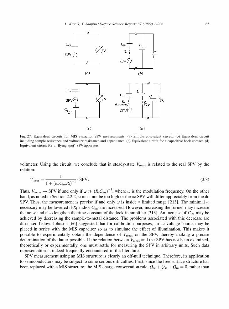
voltmeter. Using the circuit, we conclude that in steady-state Vmeas is related to the real SPV by therelation:
Vmeas � 1
1� i!CinsRi� �ÿ1� SPV: (3.8)
Thus, Vmeas ! SPV if and only if !� �RiCins�ÿ1, where ! is the modulation frequency. On the other
hand, as noted in Section 2.2.2, ! must not be too high or the ac SPV will differ appreciably from the dcSPV. Thus, the measurement is precise if and only ! is inside a limited range [213]. The minimal !necessary may be lowered if Ri and/or Cins are increased. However, increasing the former may increasethe noise and also lengthen the time-constant of the lock-in ampli®er [213]. An increase of Cins may beachieved by decreasing the sample-to-metal distance. The problems associated with this decrease arediscussed below. Johnson [66] suggested that for calibration purposes, an ac voltage source may beplaced in series with the MIS capacitor so as to simulate the effect of illumination. This makes itpossible to experimentally obtain the dependence of Vmeas on the SPV, thereby making a precisedetermination of the latter possible. If the relation between Vmeas and the SPV has not been examined,theoretically or experimentally, one must settle for measuring the SPV in arbitrary units. Such datarepresentation is indeed frequently encountered in the literature.
SPV measurement using an MIS structure is clearly an off-null technique. Therefore, its applicationto semiconductors may be subject to some serious dif®culties. First, since the free surface structure hasbeen replaced with a MIS structure, the MIS charge conservation rule, Qsc � Qss � Qm � 0, rather than
Fig. 27. Equivalent circuits for MIS capacitor SPV measurements: (a) Simple equivalent circuit. (b) Equivalent circuit
including sample resistance and voltmeter resistance and capacitance. (c) Equivalent circuit for a capacitive back contact. (d)
Equivalent circuit for a `¯ying spot' SPV apparatus.
L. Kronik, Y. Shapira / Surface Science Reports 37 (1999) 1±206 65
the free surface rule, Qsc � Qss � 0, should be used. If Qm is negligible with respect to Qsc, this isinsigni®cant. However, the metal is frequently placed within several microns from the semiconductorsurface for increasing Cins. Then, Qm is not negligible, as explained in Section 2.1.5. Mathematically,adding a constant charge density, Qm, to the free surface charge conservation rule is equivalent to theaddition of slow surface states (see Section 2.2.2). Thus, V0
s , the equilibrium value of Vs, may be alteredand a different SPV obtained. The importance of this is application dependent and is discussed whereappropriate in Sections 4 and 5.
For some applications, controlling V0s via an external bias may prove bene®cial. Here, this is easily
performed by applying a dc-bias to the metal electrode. This bias must be supplied through a largeresistor or the ensuing ac signal will be effectively short-circuited. As noted in Section 2.1.5, the effectof the applied bias on V0
s may be very small if the surface state density is large, due to screening. Thisrequires an increased electric ®eld which is typically limited by the breakdown voltage of the dielectric.Schulz et al. [214] suggested that in such cases some control of V0
s may be achieved by using aferroelectric crystal instead of a dielectric. This results in a very large electric ®eld between metal andsemiconductor due to the spontaneous polarization of the ferroelectric.
A severe problem may occur if Qm is signi®cant and ! is too low to meet the condition!� �RiCins�ÿ1
. If the capacitor has enough time to change its charge during illumination, Qm maychange appreciably and the SPV may be different than that obtained with constant Qm. Here theproblem is not that Vmeas will differ from the SPV, as in Eq. (3.8). Rather, the SPV itself will bedifferent. Consequently, it cannot be corrected by a calibration signal. Worse, the extent of the changein the SPV may depend on the intensity and the photon energy of the illumination. Thus, the measuredSPV spectrum may be very different from the real SPV spectrum. While spectra taken under suchconditions may still be (cautiously) used for qualitative purposes, any quantitative analysis of them isdubious unless the time-dependence of Qm is explicitly taken into account.
The direct reading of the SPV via off-null measurements in the MIS capacitor approach also hassome distinct advantages over the null measurements performed in the Kelvin probe approach. First, itsnoise level (and hence minimum attainable signal) is much better than that of the Kelvin probe and canbe rather easily reduced to the mV or sub-mV level [215]. Note that a mV noise level is also attained atthe output of the lock-in ampli®er used in Kelvin probe measurements. However, since there it is notthis voltage directly, but rather the dc bias used to nullify it, which is measured, the voltage resolution isdecreased. For example, detecting a 1 mV voltage across a 1 G resistor is tantamount to a currentresolution of 1 fA. For a probe capacitance of 1 pF, this implies a dc bias resolution of fA/pF �1 mV.Second, the temporal resolution of MIS structures is considerably superior to that of the Kelvin probe.Indeed, Johnson has used MIS structures as early as 1957 for measuring transient SPV responses in thems range [4].
Time-resolved measurements require that Vmeas re¯ect the real SPV over the entire time scaleinvolved. This calls for the relation between Vmeas and the SPV to be frequency independent at theentire frequency range extending between the inverses of the longest and shortest times measured.Recently, HlaÂvka and SÏvehla [216] have reexamined the frequency response of a MIS structure for SPVmeasurements, using the more general equivalent circuit shown in Fig. 27(b) [215,216], where Rs is the(often negligible) sample resistance, Ri is the Voltmeter resistance, and Ci is the Voltmeter capacitance(including lead capacitance). They have noted that Vmeas ! SPV as long as Zi � Zs, where
1=Zi ������������������������������������1=Ri�2 � �!Ci�2
qis the total input impedance of the voltmeter and Zs �
��������������������������������R2
s � �1=!Cins�2q
.
66 L. Kronik, Y. Shapira / Surface Science Reports 37 (1999) 1±206
By analyzing the circuit of Fig. 27(b), it may be shown that Vmeas ! SPV if [216]:
Ri � Rs; Cins � Ci; (3.9a)
RiCins� �ÿ1� !� RsCi� �ÿ1: (3.9b)
Inspection of Eqs. (3.9) reveals that if the prerequisite condition, (3.9a), on voltmeter resistance andcapacitance is ful®lled, the frequency response is constant in a range in which the lower bound hasalready been discussed above and the upper bound is dictated by sample resistance and voltmetercapacitance. The minimal time which can be safely measured is of the order of RsCi. Since Rs istypically small, a very good temporal resolution can be obtained even if Ci is non-negligible. Using thisapproach, a temporal resolution of 0.1 ms has been demonstrated [216]. Such a resolution is clearlymany orders of magnitude better than that afforded by a Kelvin probe. However, the MIS capacitorapproach is not suitable for following long transients. From Eq. (3.9b), the maximal time for which atransient signal can be adequately followed is bounded by RiCins, which is typically of the order ofmsec. Longer transients must therefore be followed with a Kelvin probe. Meshkov and Akimov [217]have constructed an apparatus where both the metallic electrode and the photon beam can be either®xed or modulated. This device may be operated as either a Kelvin probe or an SPV-sensing MISstructure and allows the user to enjoy the best of both worlds, depending on the application. Subsequentauthors devised other apparata which combine a Kelvin probe and a MIS structure. A recent examplemay be found in [218], where the ®xed and vibrating plates are located adjacent to each other.
Another important advantage of the MIS approach is that the Ohmic back contact, crucial for Kelvinprobe measurements, may be replaced by contactless capacitive coupling (e.g., by means of a spacer)[12]. An appropriate equivalent circuit is shown in Fig. 27(c). The capacitive coupling creates aparasitic MIS capacitor in the back of the sample. However, as long as the capacitance of the backcapacitor is much larger than that of the front capacitor, the impedance of the former will be muchsmaller that of the latter. Hence, the ac voltage on the back capacitor will be negligible and themeasurement will not lose in accuracy. This condition may be met either by decreasing the thickness ofthe back insulator (which may be dif®cult), or simply by making the back capacitor area much largerthan that of front capacitor [12].
The MIS measuring technique is amenable to scanning applications and is also used for obtainingspatially-resolved SPV maps. Kozhevin [219] provided an early demonstration of a line-scan of theSPV at a `real' MIS capacitor, by scanning the surface with a narrow, modulated, light beam. Morerecently, Munakata et al. [215] have designed a `¯ying spot' scanning SPV apparatus. The device isbased on an `arti®cial' MIS structure involving the sample under study. An illumination spot is scannedacross the surface via (one or more) cathode ray tubes. The ensuing SPV map is acquired using acomputer and displayed on a TV screen. They have extensively used this device for non-destructivemonitoring of defects and inhomogeneities (see, e.g., [213,215,220±231]). As an illustrative simpleexample, an SPV image of a Si wafer after various treatments is shown in Fig. 28 [222]. Various degreesof surface damage are easily exposed since they affect the magnitude of the obtained SPV signal.
In the `¯ying spot' approach, the metallic electrode covers the entire sample, whereas only a smallportion of the sample is illuminated at a given time. From an equivalent circuit point of view(Fig. 27(d)), the unilluminated area introduces a shunting path in parallel with the illuminated area andthe SPV signal is effectively attenuated by the ratio of the illuminated area to the overall area.Therefore, the magnitude of the signal is limited by the size of the illumination spot and not by the size
L. Kronik, Y. Shapira / Surface Science Reports 37 (1999) 1±206 67

of the capacitor. More recently, Lagowski et al. have suggested the arrangement shown in Fig. 2.29[12]. In their device, the illumination point is ®xed in space and applied to the sample via a ®ber opticcable inserted in the small metal electrode. Lateral resolution is obtained by placing the sample on amoving stage.
To conclude this section, we note that `Arti®cial' MIS capacitor arrangements for SPV measurementsare commercially available [232±235] and are applied to many interesting and technologicallyimportant quantitative analyses which are discussed in Section 5.
3.3. Other methods
3.3.1. E-beam analysis
In Section 3.1, we noted that the SPV causes a change of equal magnitude in the surface workfunction, Ws. Therefore, any method for work function measurements (and not just the Kelvin probeapproach) can be used for SPV measurements simply by detecting illumination-induced changes in Ws
(a detailed discussion of such methods may be found in, e.g., [121,155,236]). Since the Kelvin probe isone of the most sensitive and accurate methods for detecting changes in Ws, most other work function
Fig. 28. SPV images of a Si wafer: (a) Rough surface. (b) Polished surface. (c) Annealed surface (after Munakata and
Matsubara [222]).
68 L. Kronik, Y. Shapira / Surface Science Reports 37 (1999) 1±206
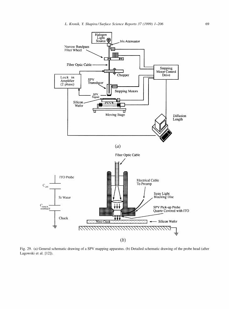
Fig. 29. (a) General schematic drawing of a SPV mapping apparatus. (b) Detailed schematic drawing of the probe head (after
Lagowski et al. [12]).
L. Kronik, Y. Shapira / Surface Science Reports 37 (1999) 1±206 69

techniques have not been used for SPV purposes. The only notable exception is the electron-beammethod [155].
This method uses an electron gun and the sample as the cathode and anode of a vacuum diode,respectively. If an electron beam impinges on the sample, the external current, I, is a monotonousfunction of Ws ÿ V , where V is the diode bias. Assuming no change in the functional form of thisdependence, a change in Ws produces a rigid horizontal shift in the I±V curve. The difference betweenV values needed to sustain a certain current (in the retarding ®eld regime of the diode) in two differentsamples is thus equal to the difference in Ws between the samples. This yields an (indirect)measurement of the CPD between two samples [160].
A similar rigid horizontal shift in the I±V curve should be obtained due to illumination-inducedchanges in Ws, where the shift is equal to the SPV. This effect has been used for SPV measurements asearly as the 1950s (e.g., by Wlerick [237] and Zyrianov [238]). As an example, the I±V curves obtainedfrom an electron gun ± CdS sample diode in the dark and under super-bandgap illumination are given incurves (I) and (II), respectively, of Fig. 30, indicating an SPV of �200 meV [239]. The current is mostsensitive to variations in Ws where the slope of the I±V curve is maximal. This is demonstrated in curve(III) of Fig. 30, which shows the difference between curves (I) and (II). Steinrisser and Hetrick [239]have used chopped illumination in conjunction with a lock-in ampli®er at a diode bias corresponding tothe maximum sensitivity. This produced an ac diode current with an amplitude of:
I � I V � SPV� � ÿ I�V� �SPV�VSPV
dI�V�dV
: (3.10)
Since at maximum sensitivity dl�V�=dV may be as high as several mÿ1, SPVs as low as 1 mV can bedetected.
Despite its elegance, use of the electron-beam method has been limited. On the one hand, use of anelectron-beam requires adequate vacuum, which restricts the applications of the technique. On the otherhand, the 1 mV sensitivity can be matched by a well-designed MIS structure. On the positive side, theinherently small lateral dimensions of the electron-beam provide for a relatively simple solution formeasuring very small samples or for performing scanning measurements. An example of the latter is
Fig. 30. Current-voltage characterics of an electron gun ± CdS sample vacuum diode: (I) in the dark, (II) under super-bandgap
illumination, (III) difference between the former two curves, in arbitrary units (after Steinrisser and Hetrick [239]).
70 L. Kronik, Y. Shapira / Surface Science Reports 37 (1999) 1±206
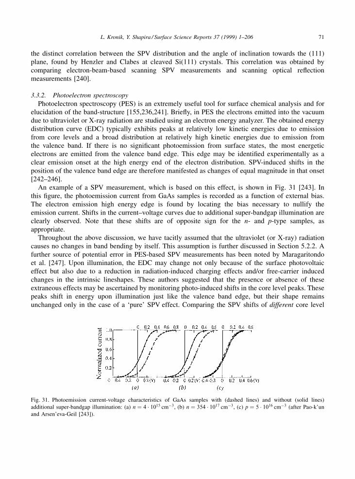
the distinct correlation between the SPV distribution and the angle of inclination towards the (111)plane, found by Henzler and Clabes at cleaved Si(111) crystals. This correlation was obtained bycomparing electron-beam-based scanning SPV measurements and scanning optical re¯ectionmeasurements [240].
3.3.2. Photoelectron spectroscopy
Photoelectron spectroscopy (PES) is an extremely useful tool for surface chemical analysis and forelucidation of the band-structure [155,236,241]. Brie¯y, in PES the electrons emitted into the vacuumdue to ultraviolet or X-ray radiation are studied using an electron energy analyzer. The obtained energydistribution curve (EDC) typically exhibits peaks at relatively low kinetic energies due to emissionfrom core levels and a broad distribution at relatively high kinetic energies due to emission fromthe valence band. If there is no signi®cant photoemission from surface states, the most energeticelectrons are emitted from the valence band edge. This edge may be identi®ed experimentally as aclear emission onset at the high energy end of the electron distribution. SPV-induced shifts in theposition of the valence band edge are therefore manifested as changes of equal magnitude in that onset[242±246].
An example of a SPV measurement, which is based on this effect, is shown in Fig. 31 [243]. Inthis ®gure, the photoemission current from GaAs samples is recorded as a function of external bias.The electron emission high energy edge is found by locating the bias necessary to nullify theemission current. Shifts in the current±voltage curves due to additional super-bandgap illumination areclearly observed. Note that these shifts are of opposite sign for the n- and p-type samples, asappropriate.
Throughout the above discussion, we have tacitly assumed that the ultraviolet (or X-ray) radiationcauses no changes in band bending by itself. This assumption is further discussed in Section 5.2.2. Afurther source of potential error in PES-based SPV measurements has been noted by Maragaritondoet al. [247]. Upon illumination, the EDC may change not only because of the surface photovoltaiceffect but also due to a reduction in radiation-induced charging effects and/or free-carrier inducedchanges in the intrinsic lineshapes. These authors suggested that the presence or absence of theseextraneous effects may be ascertained by monitoring photo-induced shifts in the core level peaks. Thesepeaks shift in energy upon illumination just like the valence band edge, but their shape remainsunchanged only in the case of a `pure' SPV effect. Comparing the SPV shifts of different core level
Fig. 31. Photoemission current-voltage characteristics of GaAs samples with (dashed lines) and without (solid lines)
additional super-bandgap illumination: (a) n � 4 � 1015 cmÿ3, (b) n � 354 � 1017 cmÿ3, (c) p � 5 � 1016 cmÿ3 (after Pao-k'un
and Arsen'eva-Geil [243]).
L. Kronik, Y. Shapira / Surface Science Reports 37 (1999) 1±206 71
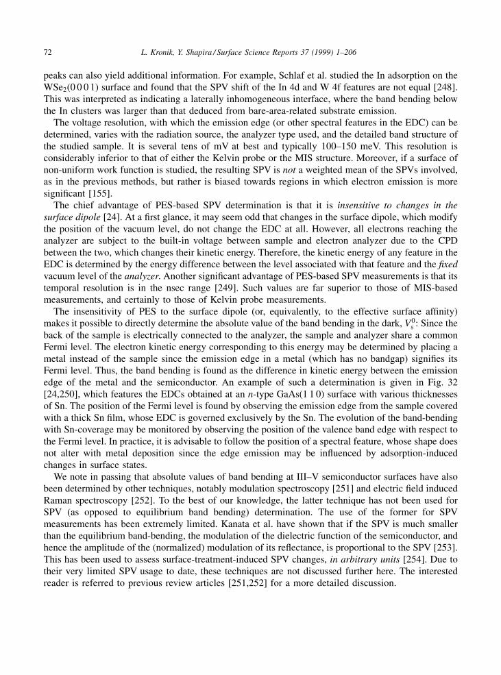
peaks can also yield additional information. For example, Schlaf et al. studied the In adsorption on theWSe2(0 0 0 1) surface and found that the SPV shift of the In 4d and W 4f features are not equal [248].This was interpreted as indicating a laterally inhomogeneous interface, where the band bending belowthe In clusters was larger than that deduced from bare-area-related substrate emission.
The voltage resolution, with which the emission edge (or other spectral features in the EDC) can bedetermined, varies with the radiation source, the analyzer type used, and the detailed band structure ofthe studied sample. It is several tens of mV at best and typically 100±150 meV. This resolution isconsiderably inferior to that of either the Kelvin probe or the MIS structure. Moreover, if a surface ofnon-uniform work function is studied, the resulting SPV is not a weighted mean of the SPVs involved,as in the previous methods, but rather is biased towards regions in which electron emission is moresigni®cant [155].
The chief advantage of PES-based SPV determination is that it is insensitive to changes in thesurface dipole [24]. At a ®rst glance, it may seem odd that changes in the surface dipole, which modifythe position of the vacuum level, do not change the EDC at all. However, all electrons reaching theanalyzer are subject to the built-in voltage between sample and electron analyzer due to the CPDbetween the two, which changes their kinetic energy. Therefore, the kinetic energy of any feature in theEDC is determined by the energy difference between the level associated with that feature and the ®xedvacuum level of the analyzer. Another signi®cant advantage of PES-based SPV measurements is that itstemporal resolution is in the nsec range [249]. Such values are far superior to those of MIS-basedmeasurements, and certainly to those of Kelvin probe measurements.
The insensitivity of PES to the surface dipole (or, equivalently, to the effective surface af®nity)makes it possible to directly determine the absolute value of the band bending in the dark, V0
s : Since theback of the sample is electrically connected to the analyzer, the sample and analyzer share a commonFermi level. The electron kinetic energy corresponding to this energy may be determined by placing ametal instead of the sample since the emission edge in a metal (which has no bandgap) signi®es itsFermi level. Thus, the band bending is found as the difference in kinetic energy between the emissionedge of the metal and the semiconductor. An example of such a determination is given in Fig. 32[24,250], which features the EDCs obtained at an n-type GaAs(1 1 0) surface with various thicknessesof Sn. The position of the Fermi level is found by observing the emission edge from the sample coveredwith a thick Sn ®lm, whose EDC is governed exclusively by the Sn. The evolution of the band-bendingwith Sn-coverage may be monitored by observing the position of the valence band edge with respect tothe Fermi level. In practice, it is advisable to follow the position of a spectral feature, whose shape doesnot alter with metal deposition since the edge emission may be in¯uenced by adsorption-inducedchanges in surface states.
We note in passing that absolute values of band bending at III±V semiconductor surfaces have alsobeen determined by other techniques, notably modulation spectroscopy [251] and electric ®eld inducedRaman spectroscopy [252]. To the best of our knowledge, the latter technique has not been used forSPV (as opposed to equilibrium band bending) determination. The use of the former for SPVmeasurements has been extremely limited. Kanata et al. have shown that if the SPV is much smallerthan the equilibrium band-bending, the modulation of the dielectric function of the semiconductor, andhence the amplitude of the (normalized) modulation of its re¯ectance, is proportional to the SPV [253].This has been used to assess surface-treatment-induced SPV changes, in arbitrary units [254]. Due totheir very limited SPV usage to date, these techniques are not discussed further here. The interestedreader is referred to previous review articles [251,252] for a more detailed discussion.
72 L. Kronik, Y. Shapira / Surface Science Reports 37 (1999) 1±206
3.4. High resolution scanning techniques
As noted above, both the scanning Kelvin probe and the scanning MIS capacitor are typically limitedto a lateral resolution of �1 mm at best, which is insuf®cient for many applications. Two high-resolution techniques for topographic mapping of surfaces have emerged in the 1980s [255]. Scanningtunneling microscopy (STM) is based on sensing the tunneling current between a tip and the sample.Atomic force microscopy (AFM) is based on sensing the de¯ection of the tip due to tip-sample forces.Both techniques have rapidly evolved and are used today for a wide range of applications [255]. In theearly 1990s both have been shown to be useful for SPV measurements as well [13±15], opening newhorizons for SPV mapping with a resolution previously unknown. The operation principles andcapabilities of these techniques are described in this section.
3.4.1. Kelvin probe force microscopy
The Kelvin force microscope is a modi®ed version of the atomic force microscope (AFM). The(contactless mode) AFM measures the de¯ection of a cantilever-mounted tip due to local forces exertedon the tip by the surface of the sample (e.g., van der Waals forces) [256]. This de¯ection is typicallymonitored by studying the optical de¯ection of a laser off the cantilever using a position sensitivedetector or by a laser interferometer. Many other schemes have also been devised [256]. Fortopographic mapping, the tip is usually vibrated at a given frequency, !1. The amplitude of the forcedvibration is in¯uenced by the tip-sample forces. Using a feedback circuit which modi®es the tip±sampledistance so as to keep the vibration amplitude constant, the tip follows the surface topography of thesample (assuming the nature of the forces has no lateral variations).
If the AFM tip is conducting (e.g., an etched gold wire, an aluminum-coated silicon nitride tip, etc.[257]) and the tip and sample are electrically connected, the electric potential and ®eld between them
Fig. 32. Ultra-violet photoemission spectroscopy EDCs of a clean (a) and Sn-covered (b±d) n-GaAs(1 1 0) surface. The
binding energy is de®ned relative to the valence band edge at the clean surface (after Mattern-Klosson and LuÈth [250]).
L. Kronik, Y. Shapira / Surface Science Reports 37 (1999) 1±206 73

are well de®ned. Then, a vertical electric force, F, given by minus the derivative of the electrostaticenergy, acts on the tip:
F � ÿ d
dz
1
2CV2
� �� ÿV2
2
dC
dz; (3.11)
where V is the voltage between the tip and the portion of sample beneath it, C, the tip±samplecapacitance, and z, the tip-to-sample distance. Martin et al. [258] used an ac voltage for V and detectedthe induced oscillation of the tip as a measure of F. However, mapping of F has proved dif®cultto translate into a mapping of V because dC=dz is neither well known nor well-controllable. Forexample, dC=dz may change due to variations in the gap dielectric constant, variations in z due toinadequate feedback control, variation in the nature of the non-electrostatic forces acting on the tip, etc.[15,259].
In 1990, Weaver et al. [15,259] have shown that Eq. (3.11) can be used for accurate surface potentialmapping if V is given by:
V � Vdc � Vac sin�!2t�: (3.12)
Inserting Eq. (3.12) in Eq. (3.11), we obtain:
F � ÿ 1
2
dC
dzV2
dc � 12
V2ac � 2VdcVac sin �!2t� ÿ 1
2V2
ac cos �2!2t�� �; (3.13)
i.e., the force acting on the tip has a dc component as well as ac components at !2 and 2!2. Inparticular, the vibration amplitude at !2 is proportional to the product VdcVac. A mixed dc and ac bias istherefore applied to the tip in order to measure the dc surface potential of a sample. A feedback loopadjusts the dc bias between tip and sample until the ac vibration of the tip at !2 is nulli®ed [15,259]. Atthis point Vdc is zero and the dc potentials of the tip and sample surface are necessarily equal. Thus, anycalibration involving dC=dz is avoided.
From a practical point of view, the voltage feedback loop can be performed simultaneously with atopographic feedback loop as they operate at different frequencies. Such a dual topography/voltagemapping arrangement is shown in Fig. 33. The topography feedback loop maintains a constantoscillation at the forced oscillation frequency, !1, by changing the tip±sample distance. Thepotentiometry loop maintains a null oscillation at the ac voltage-induced oscillation frequency, !2, byvarying the dc bias on the tip. This simple approach has been adopted by most scientists, with severalimprovements and modi®cations suggested. Kikukawa et al. [261] have used a dual resonancecantilever so that separate optimization of the two feedback loops is made possible. Yasutake [262]noted that the dc component of the electrostatic force (see Eq. (3.13)) is inherently less local than, e.g.,van der Waals forces used for topography measurements. Consequently, at each measurement point hehas deactivated the probe bias during the topography measurements and increased the lateral resolutionof the latter. For overcoming the same dif®culty, Jacobs et al. performed a surface topography scanimmediately followed by an electrical scan which retraced the same topography for each line scan[263]. In a different approach, Yokoyama and Inoue [260] have discarded the !1 feedback loopaltogether. Instead, they based the topography measurement on a second electrical feedback loop,which maintained a constant current (and hence tip-sample capacitance) at 2!2. While simple toconstruct, the resulting topography map has two disadvantages: ®rst, its resolution is reduced due to theabove mentioned less local character of the electrostatic force; second, since the feedback follows
74 L. Kronik, Y. Shapira / Surface Science Reports 37 (1999) 1±206

capacitance, rather than distance changes, the topographic map would be warped, should changes in theeffective dielectric constant occur (e.g., due to variations in a surface passivation layer).
We note in passing that any local probe, which is sensitive to both atomic and electrical forces, canbe converted into a KFM. For example, Steinke et al. have recently converted an acoustic near ®eldmicroscope into a surface-potential measuring device, using the same principles described here [264].
Nonnenmacher et al. [265] have shown that the above approach can be used for performing highresolution CPD measurements. This is because:
Vdc � VCPD � Vb; �3:14�as in Eq. (3.4) above. Therefore, tip vibration at !2 is nulli®ed when the applied bias is equal andopposite to the CPD. Since ®nding a condition at which Vb � ÿVCPD is also at the heart of the Kelvinprobe, Nonnenmacher et al. [265] have coined the name `Kelvin force microscope' (KFM) for theirapparatus. Indeed, in many respects the Kelvin probe and the KFM are very similar devices. Both arebased on ®nding an external bias which nulli®es the CPD-induced electric ®eld between an externalprobe and a sample, placed in a capacitor con®guration (see Fig. 19). However, the former is based onnullifying the ac current in the capacitor, whereas the latter is based on nullifying the ac force betweenthe capacitor electrodes. Indeed, macroscopic Kelvin-probe-like devices based on force measurements,mentioned brie¯y in Section 3.1 [146,148], are based on the operation principles outlined in Eqs. (3.13)and (3.14), albeit using a different force-measuring device. The similar operation principle dictatesmany other similarities. Both devices require adequate electrostatic shielding [257], both place similarlimits on the minimum sample conductivity which can be measured, both are useful even when there isa thin dielectric layer on top of the sample [260], and both may be operated in any ambient ifconstructed accordingly [260,261]. For example, in vacuum measurements, the damping of the forcedvibrations is reduced, resulting in long amplitude-settling times. Determination of the frequency, ratherthan the amplitude, of cantilever vibration, has been shown to be preferable for vacuum measurementsboth in terms of response time and in terms of the noise level [261].
The fundamental advantage of force measurements over current measurements is that (to ®rst order)the latter is proportional to the probe size whereas the former is independent of it. Thus, as the size of
Fig. 33. Block diagram of a dual topography/potential mapping AFM-based apparatus (after Weaver and Abraham [259]).
L. Kronik, Y. Shapira / Surface Science Reports 37 (1999) 1±206 75
the capacitor plates is shrunk (with all other experimental parameters being nominally the same), thesensitivity of the classic Kelvin probe is diminished and ®nally lost. Force measurements are notsubject to the same physical limitation. Another advantage of the KFM is that de¯ection, rather thencurrent, is being measured. Therefore, parasitic capacities in the external electronics which are a majorproblem in Kelvin probe measurements, as explained in Section 3.1, are meaningless in KFMmeasurements.
The major noise mechanism limiting the voltage resolution of KFM measurements is thermallyinduced random ¯uctuations in tip position [261,265]. The minimum measurable voltage correspondingto the noise level depends on many factors, e.g., tip radius and height, magnitude and frequency of themodulating voltage, and ®nally the quality factor of cantilever resonance and the detection bandwidth.Typically, it is in the sub-mV to 10 mV range [261,265], i.e., the KFM voltage resolution is comparableto or even better than that of a macroscopic Kelvin probe, despite its signi®cantly smaller dimensions.For good voltage resolution, it is important to avoid the trapping of stray charges on the AFM tip. Suchcharges considerably modify the electric ®eld due to the small dimensions of the tip and may alter thepotential distribution signi®cantly [259,260,265].
The spatial resolution limit of the KFM is typically several tens of nm [259,265,266]. This value isabout two to ®ve orders of magnitude better than that of most scanning Kelvin probes and one order ofmagnitude better than the record-resolution Kelvin probe mentioned in Section 3.1 [208]. As in theclassic Kelvin probe, if the work function in the area sensed by the tip is non-uniform, the measuredCPD is a weighted average of the differences CPDs present. The only difference is that in the KFM theweighting coef®cients are not the capacities between the tip and areas of different work function.Rather, they are the derivatives of these capacities, as evident from Eq. (3.13) [260,263].
Due to its promise of high-spatial-resolution surface potential measurements, the KFM has foundmany diverse applications in just a few years. These applications include work function mapping[263,265], dopant pro®ling [266±268], heterojunction imaging (in both surface [269] and cross-section[263,270] modes), circuit potentiometry [259,263,271,272], characterization of Langmuir±Blodgett®lms [273,274], and of course SPV measurements (which are based on measuring photo-induced CPDchanges). All applications but the latter are outside the scope of this review. SPV mapping using a KFMwas ®rst demonstrated by Weaver and Wickramasinghe [15], who performed SPV mapping of siliconand GaAs wafers. An illustrative example is shown in Fig. 34, which shows a photovoltage map of the(1 0 0) surface near the edge of a GaAs wafer in a (1 1 0) direction. The SPV features in the ®gure havebeen interpreted as arising from dislocations lying just below the sample surface. Thus, using the KFMinformation similar to that in Fig. 28 can be obtained, with a much higher spatial resolution.
Having discussed KFM principles and applications, we now describe several phenomena which arepotential sources of artifacts in KFM readings and must be taken into account when interpretingexperimental data: Just as the Kelvin probe, the KFM is also susceptible to systematic errors in CPDreading due to stray capacitance [263,266,268,271], as described in detail in Section 3.1. In the idealtreatment presented above, we have assumed that all capacitance is due to the tip apex only. In practice,contribution from the tip side-walls and from the cantilever can be very signi®cant. Accordingly,spacing-dependent CPD readings have been obtained [271]. Fortunately, KFM readings are usuallyperformed with topography-mapping, i.e., active spacing-control which reduces the variation in theCPD error is built-in [266]. CPD changes which were `smeared-out' spatially and whose magnitude wassmaller than the true changes by a multiplicative factor were also attributed to stray capacitance [266].Hochwitz et al. [268] studied a model in which the main parasitic capacitance was due to cantilever-
76 L. Kronik, Y. Shapira / Surface Science Reports 37 (1999) 1±206
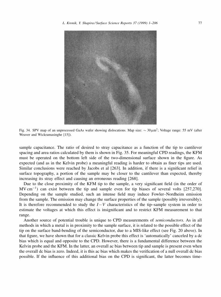
sample capacitance. The ratio of desired to stray capacitance as a function of the tip to cantileverspacing and area ratios calculated by them is shown in Fig. 35. For meaningful CPD readings, the KFMmust be operated on the bottom left side of the two-dimensional surface shown in the ®gure. Asexpected (and as in the Kelvin probe) a meaningful reading is harder to obtain as ®ner tips are used.Similar conclusions were reached by Jacobs et al [263]. In addition, if there is a signi®cant relief insurface topography, a portion of the sample may be closer to the cantilever than expected, therebyincreasing its stray effect and causing an erroneous reading [268].
Due to the close proximity of the KFM tip to the sample, a very signi®cant ®eld (in the order ofMV cmÿ1) can exist between the tip and sample even for tip biases of several volts [257,270].Depending on the sample studied, such an intense ®eld may induce Fowler±Nordheim emissionfrom the sample. The emission may change the surface properties of the sample (possibly irreversibly).It is therefore recommended to study the IÿV characteristics of the tip±sample system in order toestimate the voltages at which this effect is insigni®cant and to restrict KFM measurement to thatrange.
Another source of potential trouble is unique to CPD measurements of semiconductors. As in allmethods in which a metal is in proximity to the sample surface, it is related to the possible effect of thetip on the surface band-bending of the semiconductor, due to a MIS-like effect (see Fig. 20 above). Inthat ®gure, we have shown that for a classic Kelvin probe this effect is `automatically' canceled by a dcbias which is equal and opposite to the CPD. However, there is a fundamental difference between theKelvin probe and the KFM. In the latter, an overall ac bias between tip and sample is present even whenthe overall dc bias is zero. Indeed, it is this ac bias which makes the veri®cation of a null overall dc biaspossible. If the in¯uence of this additional bias on the CPD is signi®cant, the latter becomes time-
Fig. 34. SPV map of an unprocessed GaAs wafer showing dislocations. Map size: � 30mm2; Voltage range: 55 mV (after
Weaver and Wickramasinghe [15]).
L. Kronik, Y. Shapira / Surface Science Reports 37 (1999) 1±206 77

dependent, i.e., Eq. (3.13) should be generalized to the form:
F � ÿ 1
2
dC
dzVb � V Ideal
CPD ��VCPD�t� � Vac sin�!2t�� �2; (3.15)
where V IdealCPD is the CPD in the absence of tip-induced band-bending, and �VCPD�t� is the time-
dependent tip-induced change in CPD.If �VCPD�t� has no dc component (i.e., if changing the polarity of Vb changes the sign of �VCPD�t�
without changing its magnitude), the force component at !2 remains unaffected and the CPDmeasurement is valid (although using the 2!2 component for topography would fail). Unfortunately,this does not have to be the case. It is well known that the bias dependence of the band bending at anMIS structure is highly non-symmetric [25]. Essentially, this is because biases of opposite polaritiespush the surface band bending in the opposite directions of inversion and accumulation (seeSection 2.1.3). Under such conditions, the measured value of the CPD does not re¯ect its true value.
The possible effects of ac-bias-dependent CPD readings have been elegantly demonstrated by Lenget al. [270]. These authors have studied CPD variations across a cleaved cross-section of a GaAs/GaInP(disordered)/GaInP(ordered) structure. The dependence of the CPD on the ac-bias for each of thethree regions is shown in Fig. 36. While the apparent CPDs at the GaAs and the ordered GaInP regionswere bias-independent, the apparent CPD at the disordered GaInP region was highly bias-dependent.Leng et al. have concluded that, in the former two regions, the band-bending is pinned by surface stateswhich screen out the tip-induced ®eld, whereas the disordered GaInP surface is unpinned and istherefore very sensitive to the tip bias. (For completeness, we note that they have not ruled out Fowler±Nordheim effects as the cause of the bias-dependent CPD reading since they have not studied tip±sample IÿV curves). More recently, ac bias-dependent KFM readings have also been obtained byArakawa et al. [272].
It is usually convenient to work with sizable ac biases since this increases the amplitude of themeasured ac force (see Eq. (3.13)) and hence the SNR. However, the results shown in Fig. 36 should
Fig. 35. Relative contribution of tip-sample capacitance to the total probe-sample capacitance as a function of cantilever/tip
area and spacing ratios (Ac=At and Zc=Zt, respectively) at a topographically ¯at surface and a ®xed tip-sample spacing (after
Hochwitz et al. [268]).
78 L. Kronik, Y. Shapira / Surface Science Reports 37 (1999) 1±206
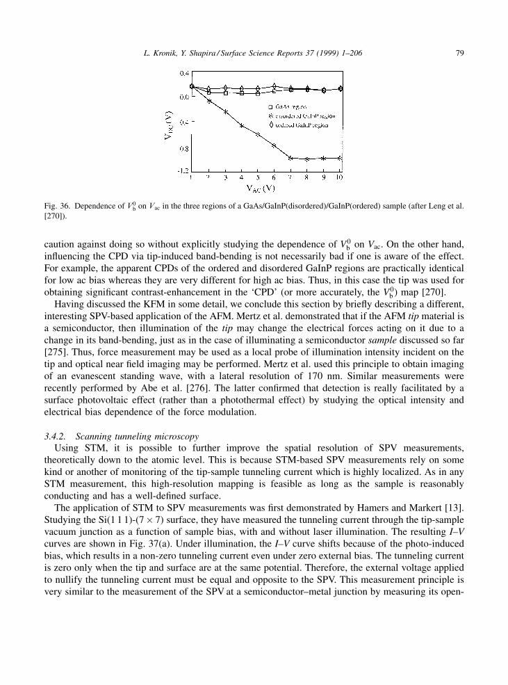
caution against doing so without explicitly studying the dependence of V0b on Vac. On the other hand,
in¯uencing the CPD via tip-induced band-bending is not necessarily bad if one is aware of the effect.For example, the apparent CPDs of the ordered and disordered GaInP regions are practically identicalfor low ac bias whereas they are very different for high ac bias. Thus, in this case the tip was used forobtaining signi®cant contrast-enhancement in the `CPD' (or more accurately, the V0
b ) map [270].Having discussed the KFM in some detail, we conclude this section by brie¯y describing a different,
interesting SPV-based application of the AFM. Mertz et al. demonstrated that if the AFM tip material isa semiconductor, then illumination of the tip may change the electrical forces acting on it due to achange in its band-bending, just as in the case of illuminating a semiconductor sample discussed so far[275]. Thus, force measurement may be used as a local probe of illumination intensity incident on thetip and optical near ®eld imaging may be performed. Mertz et al. used this principle to obtain imagingof an evanescent standing wave, with a lateral resolution of 170 nm. Similar measurements wererecently performed by Abe et al. [276]. The latter con®rmed that detection is really facilitated by asurface photovoltaic effect (rather than a photothermal effect) by studying the optical intensity andelectrical bias dependence of the force modulation.
3.4.2. Scanning tunneling microscopy
Using STM, it is possible to further improve the spatial resolution of SPV measurements,theoretically down to the atomic level. This is because STM-based SPV measurements rely on somekind or another of monitoring of the tip-sample tunneling current which is highly localized. As in anySTM measurement, this high-resolution mapping is feasible as long as the sample is reasonablyconducting and has a well-de®ned surface.
The application of STM to SPV measurements was ®rst demonstrated by Hamers and Markert [13].Studying the Si(1 1 1)-(7� 7) surface, they have measured the tunneling current through the tip-samplevacuum junction as a function of sample bias, with and without laser illumination. The resulting I±Vcurves are shown in Fig. 37(a). Under illumination, the I±V curve shifts because of the photo-inducedbias, which results in a non-zero tunneling current even under zero external bias. The tunneling currentis zero only when the tip and surface are at the same potential. Therefore, the external voltage appliedto nullify the tunneling current must be equal and opposite to the SPV. This measurement principle isvery similar to the measurement of the SPV at a semiconductor±metal junction by measuring its open-
Fig. 36. Dependence of V0b on Vac in the three regions of a GaAs/GaInP(disordered)/GaInP(ordered) sample (after Leng et al.
[270]).
L. Kronik, Y. Shapira / Surface Science Reports 37 (1999) 1±206 79
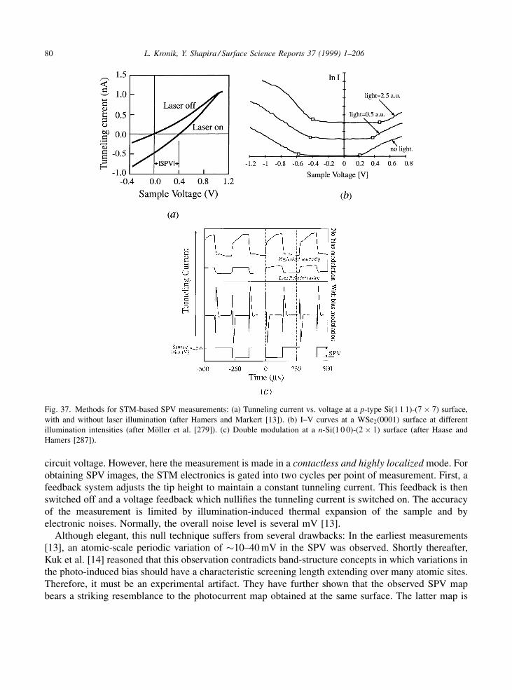
circuit voltage. However, here the measurement is made in a contactless and highly localized mode. Forobtaining SPV images, the STM electronics is gated into two cycles per point of measurement. First, afeedback system adjusts the tip height to maintain a constant tunneling current. This feedback is thenswitched off and a voltage feedback which nulli®es the tunneling current is switched on. The accuracyof the measurement is limited by illumination-induced thermal expansion of the sample and byelectronic noises. Normally, the overall noise level is several mV [13].
Although elegant, this null technique suffers from several drawbacks: In the earliest measurements[13], an atomic-scale periodic variation of �10±40 mV in the SPV was observed. Shortly thereafter,Kuk et al. [14] reasoned that this observation contradicts band-structure concepts in which variations inthe photo-induced bias should have a characteristic screening length extending over many atomic sites.Therefore, it must be an experimental artifact. They have further shown that the observed SPV mapbears a striking resemblance to the photocurrent map obtained at the same surface. The latter map is
Fig. 37. Methods for STM-based SPV measurements: (a) Tunneling current vs. voltage at a p-type Si(1 1 1)-(7� 7) surface,
with and without laser illumination (after Hamers and Markert [13]). (b) I±V curves at a WSe2(0001) surface at different
illumination intensities (after MoÈller et al. [279]). (c) Double modulation at a n-Si(1 0 0)-(2� 1) surface (after Haase and
Hamers [287]).
80 L. Kronik, Y. Shapira / Surface Science Reports 37 (1999) 1±206
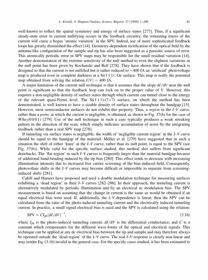
well-known to re¯ect the spatial symmetry and energy of surface states [277]. Thus, if a signi®cantsteady-state error in current nullifying occurs in the feedback circuitry, the remaining traces of thecurrent will cause a bogus `atomic variation' in the SPV. Indeed, use of more sophisticated feedbackloops has greatly diminished the effect [14]. Geometry-dependent recti®cation of the optical ®eld by theantenna-like con®guration of the sample and tip has also been suggested as a parasitic source of error.This atomically periodic error in SPV maps may be responsible for the small residual variation [14].Another demonstration of the extreme sensitivity of the null method to even the slightest variations inthe null point has been given by Kochanski and Bell [278]. They have shown that if the feedback isdesigned so that the current is not nulli®ed but is rather reduced to �400 fA an `arti®cial' photovoltagemap is produced even in complete darkness at a Si(1 1 1) : Ge surface. This map is really the potentialmap obtained from solving the relation I�V� � 400 fA.
A major limitation of the current null technique is that it assumes that the slope dI=dV near the nullpoint is signi®cant so that the feedback loop can lock on to the proper value of V . However, thisrequires a non-negligible density of surface states through which current can tunnel close to the energyof the relevant quasi-Fermi level. The Si(1 1 1)-(7�7) surface, on which the method has beendemonstrated, is well known to have a sizable density of surface states throughout the bandgap [13].However, most semiconductor surfaces do not exhibit this property. Thus, a region in the I±V curve,rather than a point, at which the current is negligible, is obtained, as shown in Fig. 37(b) for the case ofWSe2(0 0 0 1) [279]. Use of the null technique in such a case typically produces a weak streakingpattern in the direction of the scan, which simply indicates accumulation of noise by the integratingfeedback rather than a real SPV map [278].
If tunneling via surface states is negligible, the width of `negligible current region' in the I±V curveshould be equal to the bandgap of the material. MoÈller et al. [279] have suggested that in such asituation the shift of either `knee' at the I±V curve, rather than its null point, is equal to the SPV (seeFig. 37(b)). While valid for the speci®c surface studied, this method also suffers from signi®cantdrawbacks. The `¯at region' in such I±V curves is frequently larger than the material bandgap becauseof additional band-bending induced by the tip bias [280]. This effect tends to decrease with increasingillumination intensity due to increased free carrier screening of the bias-induced ®eld. Consequently,photovoltaic shifts in the I±V curves may become dif®cult or impossible to separate from screening-induced shifts [281].
Cahill and Hamers have proposed and used a double modulation technique for measuring surfacesexhibiting a `dead region' in their I±V curves [282±286]. In their approach, the tunneling current isalternatively modulated by periodic illumination and by an electrical ac modulation bias. The SPVmeasurement is based on assuming that the change in current is the same as would be obtained if anequal electrical bias were used. If, additionally, the I±V dependence is linear, then the SPV can becalculated from the ratio of the photo-induced tunneling current and the electrically induced tunnelingcurrent. In practice, a small signal electrical bias is used and the SPV is calculated using the relation:
SPV � CIph�dI=dV�ÿ1; (3.16)
where Iph is the photo-induced tunneling current, dI=dV is the differential conductance, and C is aconstant which compensates for the different wave-forms of the optical and electrical signals. Thistechnique can be applied at any dc electrical bias between the tip and sample and may therefore alwaysbe operated outside the `dead region' of the I±V curve. The real I±V response is clearly non-linear andmay render Eq. (3.16) invalid in the general case. For the speci®c cases studied, it has been estimated to
L. Kronik, Y. Shapira / Surface Science Reports 37 (1999) 1±206 81

introduce an error of only several percent [285,286]. The major disadvantage of this technique is that allmeasurements are conducted in the presence of a ®nite photo-induced tunneling current. This currentcan charge the surface and is discussed in more detail below.
McEllistrem et al. [280] have suggested a synchronized null method. At a ®xed dc bias, choppedillumination which results in a modulated photocurrent is applied. Then, an ac bias which issynchronized with the illumination is applied so as to nullify the modulation in the photocurrent. Thesynchronized null enjoys the advantages of the regular null technique but circumvents the dif®cultiesassociated with the `dead region' in the I±V curve, due to the added ac bias. An example of the appli-cation of this technique to a n-Si(1 0 0)-(2� 1) surface is shown in Fig. 37(c) [287]. With no ac bias andlow illumination intensities, a clear modulation of the photocurrent is observed. With the proper ac bias,the ac current is nulli®ed, except for current `spikes' which result from capacitive coupling of the acbias and are irrelevant. At high illumination intensities, the tunneling current features two timeconstants ± a short one, associated with the electronic response, and a long one, associated with sampleheating. Clearly, nullifying the current after the short time constant only should be used in such a case.
It is very important to realize that all four STM-based SPV measurement techniques are prone toin¯uence from the measurement tip. In both the simple and the synchronized null schemes, an electric®eld exists between sample and tip due to the CPD between them and/or the applied bias. This ®eldmay affect the surface potential of the sample. Due to the feedback loop, the overall (internal andexternal) voltage drop between tip and sample remains constant upon illumination. Using Eq. (2.41),this implies that Qm, the metal charge, is constant, and hence the interference of the tip is limited to achange in V0
s , as in the case of the MIS structure. The situation is quite different for the other twotechniques. We have already discussed how tip-induced biases can hamper the analysis of shifts in theI±V curves. In the double modulation technique, in addition to the possible surface charging mentionedabove, the tip-to-sample voltage drop (and hence Qm) does not remain constant upon illumination. Thismay further change the acquired SPV with respect to that present in the absence of the tip. Therefore,any discussion of obtained SPV features cannot be separated from an evaluation of possibleinterference of the measurement technique.
Having fully examined the principles, advantages, and disadvantages of STM-based SPVmeasurement techniques, we turn to examin the spatially-resolved information which can be extractedusing these tools. Hamers and Markert [13] and Kuk et al. [14] have observed atomic-scale spatialchanges (i.e., with a diameter of several tens of AÊ ) in the SPV at the Si(1 1 1)-(7� 7) surface using thesimple null technique. An example is shown in Fig. 38. Both groups have argued that such a well-resolved feature should be produced by a trap-related local variation in band bending and/orrecombination rate. This is because the surface Debye screening length at the surface-state rich surfaceis expected to be signi®cantly shorter than that of the bulk. This is a result of the high density of surfacestates, of surface segregation of the dopant, and of enhanced screening due to the photocarriers.However, subsequent measurements of clean, Ge-adsorbed [278], Ag-adsorbed [283], and K-adsorbed[284] Si(1 1 1)-(7� 7), Si(0 0 1) [282,285], and Si(1 1 1)-(2� 1) [286] surfaces produced microscopi-cally uniform SPVs unless charging effects, due to ®nite tunneling currents, were present. The latterpoint is well-demonstrated in Fig. 39 [282] which clearly shows how all spatially-resolved SPV featuresobtained at an n-Si(0 0 1) surface using the double modulation technique are strongly reduced as thetunneling current is decreased. This is not necessarily a disadvantage of the double modulationtechnique. While originally a `parasitic effect', the ®nite current enhances local-defect-induced SPVsand thus provides much new information.
82 L. Kronik, Y. Shapira / Surface Science Reports 37 (1999) 1±206
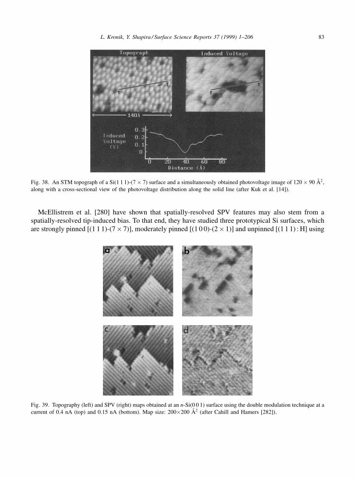
McEllistrem et al. [280] have shown that spatially-resolved SPV features may also stem from aspatially-resolved tip-induced bias. To that end, they have studied three prototypical Si surfaces, whichare strongly pinned [(1 1 1)-(7� 7)], moderately pinned [(1 0 0)-(2� 1)] and unpinned [(1 1 1) : H] using
Fig. 38. An STM topograph of a Si(1 1 1)-(7� 7) surface and a simultaneously obtained photovoltage image of 120� 90 AÊ 2,
along with a cross-sectional view of the photovoltage distribution along the solid line (after Kuk et al. [14]).
Fig. 39. Topography (left) and SPV (right) maps obtained at an n-Si(0 0 1) surface using the double modulation technique at a
current of 0.4 nA (top) and 0.15 nA (bottom). Map size: 200�200 AÊ 2 (after Cahill and Hamers [282]).
L. Kronik, Y. Shapira / Surface Science Reports 37 (1999) 1±206 83
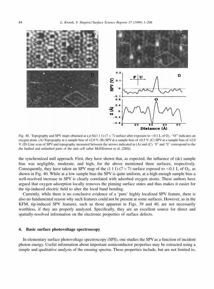
the synchronized null approach. First, they have shown that, as expected, the in¯uence of (dc) samplebias was negligible, moderate, and high, for the above mentioned three surfaces, respectively.Consequently, they have taken an SPV map of the (1 1 1)-(7� 7) surface exposed to �0.1 L of O2, asshown in Fig. 40. While at a low sample bias the SPV is quite uniform, at a high enough sample bias awell-resolved increase in SPV is clearly correlated with adsorbed oxygen atoms. These authors haveargued that oxygen adsorption locally removes the pinning surface states and thus makes it easier forthe tip-induced electric ®eld to alter the local band bending.
Currently, while there is no conclusive evidence of a `pure' highly localized SPV feature, there isalso no fundamental reason why such features could not be present at some surfaces. However, as in theKFM, tip-induced SPV features, such as those apparent in Figs. 39 and 40, are not necessarilyworthless, if they are properly analyzed. Speci®cally, they are an excellent source for direct andspatially-resolved information on the electronic properties of surface defects.
4. Basic surface photovoltage spectroscopy
In elementary surface photovoltage spectroscopy (SPS), one studies the SPV as a function of incidentphoton energy. Useful information about important semiconductor properties may be extracted using asimple and qualitative analysis of the ensuing spectra. These properties include, but are not limited to,
Fig. 40. Topography and SPV maps obtained at a p-Si(1 1 1)-(7� 7) surface after exposure to �0.1 L of O2. `̀ O'' indicates an
oxygen atom. (A) Topography at a sample bias of +2.0 V. (B) SPV at a sample bias of +0.5 V. (C) SPV at a sample bias of +2.0
V. (D) Line scan of SPV and topography measured between the arrows indicated in (A) and (C). `F' and `U' correspond to the
the faulted and unfaulted parts of the unit cell (after McEllistrem et al. [280]).
84 L. Kronik, Y. Shapira / Surface Science Reports 37 (1999) 1±206
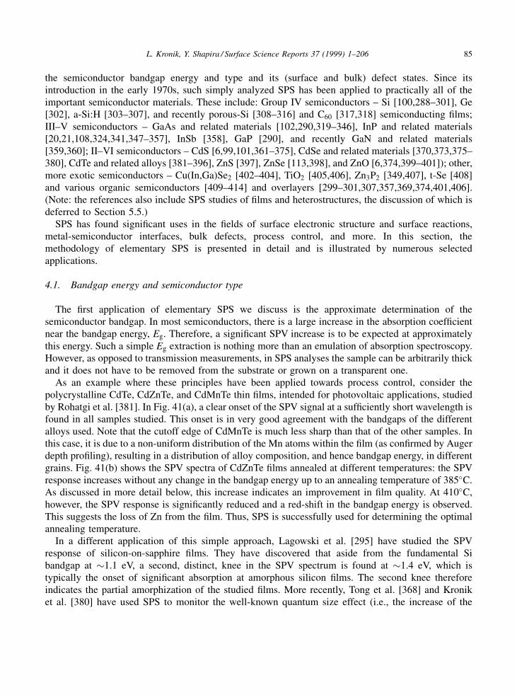
the semiconductor bandgap energy and type and its (surface and bulk) defect states. Since itsintroduction in the early 1970s, such simply analyzed SPS has been applied to practically all of theimportant semiconductor materials. These include: Group IV semiconductors ± Si [100,288±301], Ge[302], a-Si:H [303±307], and recently porous-Si [308±316] and C60 [317,318] semiconducting ®lms;III±V semiconductors ± GaAs and related materials [102,290,319±346], InP and related materials[20,21,108,324,341,347±357], InSb [358], GaP [290], and recently GaN and related materials[359,360]; II±VI semiconductors ± CdS [6,99,101,361±375], CdSe and related materials [370,373,375±380], CdTe and related alloys [381±396], ZnS [397], ZnSe [113,398], and ZnO [6,374,399±401]); other,more exotic semiconductors ± Cu(In,Ga)Se2 [402±404], TiO2 [405,406], Zn3P2 [349,407], t-Se [408]and various organic semiconductors [409±414] and overlayers [299±301,307,357,369,374,401,406].(Note: the references also include SPS studies of ®lms and heterostructures, the discussion of which isdeferred to Section 5.5.)
SPS has found signi®cant uses in the ®elds of surface electronic structure and surface reactions,metal-semiconductor interfaces, bulk defects, process control, and more. In this section, themethodology of elementary SPS is presented in detail and is illustrated by numerous selectedapplications.
4.1. Bandgap energy and semiconductor type
The ®rst application of elementary SPS we discuss is the approximate determination of thesemiconductor bandgap. In most semiconductors, there is a large increase in the absorption coef®cientnear the bandgap energy, Eg. Therefore, a signi®cant SPV increase is to be expected at approximatelythis energy. Such a simple Eg extraction is nothing more than an emulation of absorption spectroscopy.However, as opposed to transmission measurements, in SPS analyses the sample can be arbitrarily thickand it does not have to be removed from the substrate or grown on a transparent one.
As an example where these principles have been applied towards process control, consider thepolycrystalline CdTe, CdZnTe, and CdMnTe thin ®lms, intended for photovoltaic applications, studiedby Rohatgi et al. [381]. In Fig. 41(a), a clear onset of the SPV signal at a suf®ciently short wavelength isfound in all samples studied. This onset is in very good agreement with the bandgaps of the differentalloys used. Note that the cutoff edge of CdMnTe is much less sharp than that of the other samples. Inthis case, it is due to a non-uniform distribution of the Mn atoms within the ®lm (as con®rmed by Augerdepth pro®ling), resulting in a distribution of alloy composition, and hence bandgap energy, in differentgrains. Fig. 41(b) shows the SPV spectra of CdZnTe ®lms annealed at different temperatures: the SPVresponse increases without any change in the bandgap energy up to an annealing temperature of 385�C.As discussed in more detail below, this increase indicates an improvement in ®lm quality. At 410�C,however, the SPV response is signi®cantly reduced and a red-shift in the bandgap energy is observed.This suggests the loss of Zn from the ®lm. Thus, SPS is successfully used for determining the optimalannealing temperature.
In a different application of this simple approach, Lagowski et al. [295] have studied the SPVresponse of silicon-on-sapphire ®lms. They have discovered that aside from the fundamental Sibandgap at �1.1 eV, a second, distinct, knee in the SPV spectrum is found at �1.4 eV, which istypically the onset of signi®cant absorption at amorphous silicon ®lms. The second knee thereforeindicates the partial amorphization of the studied ®lms. More recently, Tong et al. [368] and Kroniket al. [380] have used SPS to monitor the well-known quantum size effect (i.e., the increase of the
L. Kronik, Y. Shapira / Surface Science Reports 37 (1999) 1±206 85

bandgap with decreasing crystallite size) at nanocrystalline CdS and CdSe quantum dot ®lms,respectively.
While the simple analysis described above is quite useful, one must bear in mind that it is onlyapproximate. In Fig. 41, the nominal bandgap is indeed within the onset of the largest SPV signal.However, this onset is relatively broad, the exact position of Eg within it is by no means obvious, and
Fig. 41. SPV spectra of: (a) (i) MBE-grown CdTe (Eg=1.45 eV), (ii) MOCVD-grown CdTe (Eg=1.45 eV), (iii) MBE-grown
CdZnTe (Eg=1.7 eV), and (iv) MOCVD-grown CdMnTe (Eg=1.7 eV) polycrystalline ®lms grown on glass/SnO2/CdS
substrates. (b) CdZnTe ®lms annealed at different temperatures in air for 30 minutes (after Rohatgi et al. [381]).
Fig. 42. SPV spectra of: (a) An n-type GaAs(1 1 0) surface, UHV cleaved (top curve) and with a 4 AÊ Al overlayer (bottom
curve). (b) A p-type InP(1 1 0) surface, UHV cleaved (top curve) and with a 4 AÊ Au overlayer (bottom curve) (after Burstein
et al. [324]).
86 L. Kronik, Y. Shapira / Surface Science Reports 37 (1999) 1±206

the error associated with determining Eg may be as large as 0.2 eV in some cases. This observation istrue even for clean surfaces of high quality single crystals, as clearly shown in Fig. 42 [324], whichfeatures the SPV spectra of n-type GaAs and p-type InP (other aspects of this ®gure are discussedbelow).
The broad onset of the super-bandgap SPV is due to two distinct absorption mechanism for photonswith an energy slightly below Eg: ®rst, a non-negligible electric ®eld is always associated with asigni®cant SCR. Therefore, sub-bandgap absorption which is electric-®eld-assisted (i.e., the Franz±Keldysh effect, already mentioned in Section 2.2.3) is expected to blur the sharp onset of the absorption[415]. Second, photo-assisted charge transfer may take place between shallow states extending from thebandgap (also known as `tail states') and one of the bands [295,303,316]. This induces a gap-staterelated SPV, as explained in Section 2.2.3, which may also blur the onset of the super-bandgap SPV. Acase in point is the SPV spectra of silicon-on-sapphire samples taken by Lagowski et al. [295], shown inFig. 43. In this case, ion implantation is known to produce both valence and conduction band tail states.At 230 K, charge transfer between the tail states, complemented by thermal emission of carriers intothe bands, masks the super-bandgap SPV so effectively that the position of Eg cannot be determined atall. At 130 K, however, the thermal step, and therefore the crucial step of charge separation, aresuppressed, and the Eg related onset is clearly visible. Note that the effects of sub-bandgap absorptiontails are usually considerably more noticeable in SPS than in absorption spectroscopy. This is because,as explained in Section 2.2.3, SPS is inherently much more sensitive to sub-bandgap effects in thesurface and SCR than absorption spectroscopy. While this inherent sensitivity is in many cases adistinct advantage, it is a disadvantage when trying to determine Eg.
Due to the near-Eg parasitic mechanisms, it is very seldom the case that a relatively accurate value ofEg can be obtained from the ®gure simply by inspection [327]. In fact, we are aware of only one suchcase [328]. Lassabatere et al. [329] suggested to use the maximum of the derivative of the SPV signalwith respect to the photon wavelength as indicative of the bandgap, and obtained results of thetemperature dependence of the GaAs bandgap which were in very good agreement with the literature.This approach has also been used by Kuzminski and Szaynok [387].
Fig. 43. SPV spectra of a silicon-on-sapphire sample at two temperatures (after Lagowski et al. [295]).
L. Kronik, Y. Shapira / Surface Science Reports 37 (1999) 1±206 87
A mathematical analysis shows that this procedure is justi®ed if sub-bandgap absorption decaysexponentially below the bandgap energy [416] (and the SPV spectrum closely follows the absorptionspectrum [417] ± see below). However, the position of the derivative maximum may considerablydeviate from Eg in the presence of a signi®cant Franz±Keldysh effect [98] or an arbitrary distributionof tail states. For example, Lagowski et al. determined that a structure in the second derivative of theSPV spectrum, near the bandgap energy of GaAs, was actually due to residual impurities [333]. Thiswas accomplished by observing that this structure is independent of an applied magnetic ®eld. It hasbeen our experience that the error associated with Eg determination is frequently (but not always)improved to a several tens of meV at most when using the derivative approach on single crystals.Usually, we have found no improvement in accuracy when applying the same procedure topolycrystalline samples.
With the non-ideal mechanisms cited, Eg should no longer be treated as an outstanding numericalthreshold. Rather, it should be treated as a ®tting parameter (albeit a very important one), as usuallydone when interpreting absorption spectra. In order to apply such an approach to SPS data, it isimportant to consider how well SPV spectra are expected to resemble absorption spectra. Detailedexperimental comparisons between SPV and absorption spectra reveal that the two are often similar, butnever identical [102,409,410]. Let us consider the sources of this discrepancy: ®rst, the SPV isproportional to the excess carrier density only for a low enough injection of excess carriers, �n (seeEq. (2.57)). For higher injection levels, a sub-linear dependence of SPV on �n is expected (seeSection 5.2 below). The increase of the absorption coef®cient, �, with increasing photon energy,increases the injection level and may therefore decrease the SPV/�n ratio. Consequently, the rise of theSPV with increasing photon energy may be slower than that of �. We note that �n is typicallyproportional to the illumination intensity, I (see Eq. (2.61)). Thus, the attainment of an injection levelwhich is low enough to assure a constant SPV/�n ratio, may be ascertained experimentally by means ofexamining the linearity between the SPV and I.
While a low I is a necessary condition for a meaningful comparison between SPV and absorptionspectra, it is not a suf®cient one. Using Eq. (2.61), it is easy to see that the SPV is proportional to theabsorption coef®cient, �, only if the condition �L� 1 is satis®ed [290,333]. In many cases, theabsorption coef®cient increases with increasing photon energy, so that this condition is ultimatelyviolated. Thus, the SPV/I ratio decreases with increasing photon energy. This is another reason why,while � typically increases with increasing photon energy, the SPV may (following its super-bandgaponset) increase at a much slower rate or even reach a plateau (as in Fig. 42), depending on the ratiobetween � and L.
Yet another reason for the difference between SPV and absorption spectra has to do with the relationbetween �n and I. Eq. (2.61) predicts a monotonous dependence of the SPV on the absorptioncoef®cient. However, this equation is only an approximation which assumes an effective SRV ratherthan considering SCR effects in detail. A more rigorous analysis [325] shows that if, e.g., the surfacebarrier is not too high and a signi®cant recombination ¯ow is directed toward the surface, increasing �may actually decrease the SPV signal. This is because as the free carriers are generated closer to thesurface, surface recombination becomes more dominant, the net excess carrier density is diminished,and the resulting SPV signal is decreased. Accordingly, SPV versus photon energy spectra have beenobserved to change from monotonically increasing to displaying a maximum upon, e.g., hydrostaticpressure which increased the SRV [327], or background white light which reduced the barrier height[325]. A very pronounced peak is found in the SPV spectrum corresponding to the MOCVD-grown
88 L. Kronik, Y. Shapira / Surface Science Reports 37 (1999) 1±206

CdTe sample in Fig. 41(a). The drastic difference between the SPV spectra of the MOCVD- and MBE-grown CdTe ®lms in this ®gure can therefore be assigned to major differences in sample parameters,such as the surface barrier, the SRV, and the diffusion length (a detailed study of these differenceswould require quantitative analysis). We note that while a peak in the spectral response is ubiquitous inphotoconductivity spectra [418], it is much less frequent in SPS curves. This is because thephotocurrent directly re¯ects the overall excess carrier density whereas the SPV is a much weakerfunction of it.
If experimental conditions are such that the super-bandgap SPV is indicative of absorption, Eg maybe reliably extrapolated [290,304,328] using the simple relations:
SPV � � � �h� ÿ Eg�2 for indirect gap semiconductors; (4.1a)
SPV � � � ����������������h� ÿ Eg
pfor direct gap semiconductors: (4.1b)
An application of this procedure to GaP is shown in Fig. 44 [290]. First, the indirect energy gap isdetermined by ®tting Eq. (4.1a) (Fig. 44(a)). The indirect-absorption contribution to the SPV is thensubtracted out and the remaining SPV is attributed to direct-gap transitions. Finally, the direct bandgapis determined by ®tting Eq. (4.1b) to the remaining SPV (see Fig. 44(b)).
We now turn our attention to determining the type (p or n) of the semiconductor. This may beachieved with the help of the sign of the knee associated with the SPV onset. Most semiconductorsurfaces are either depleted or inverted, which means that the bands of p-type semiconductors are bentdownwards towards the surface, whereas the bands of n-type semiconductors are bent upwards. Asexplained in the Section 2.2.2, super-bandgap illumination typically tends to decrease the surface band-bending. Due to the different signs of the equilibrium surface potential, this would result in a positiveSPV in n-type semiconductors and a negative SPV in p-type semiconductors. For example, the SPVspectra of n-type GaAs and p-type InP, shown in Fig. 42, clearly feature opposite onset signs. Note thatin this ®gure, as well as in some of the following ones, changes in the CPD, rather the SPV, are plotted,
Fig. 44. SPV spectra of a GaP(1 0 0) surface: (a) Extrapolation of the indirect bandgap. (b) Extrapolation of the direct
bandgap following the subtraction of the indirect bandgap contribution (after Adamowicz and Szuber [290]).
L. Kronik, Y. Shapira / Surface Science Reports 37 (1999) 1±206 89
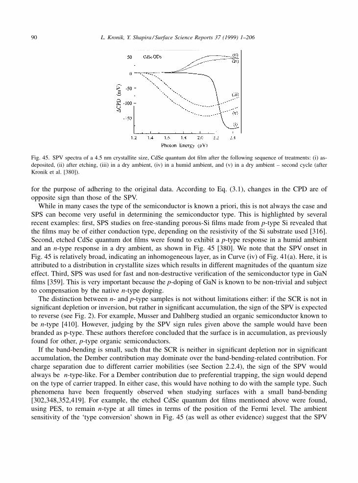
for the purpose of adhering to the original data. According to Eq. (3.1), changes in the CPD are ofopposite sign than those of the SPV.
While in many cases the type of the semiconductor is known a priori, this is not always the case andSPS can become very useful in determining the semiconductor type. This is highlighted by severalrecent examples: ®rst, SPS studies on free-standing porous-Si ®lms made from p-type Si revealed thatthe ®lms may be of either conduction type, depending on the resistivity of the Si substrate used [316].Second, etched CdSe quantum dot ®lms were found to exhibit a p-type response in a humid ambientand an n-type response in a dry ambient, as shown in Fig. 45 [380]. We note that the SPV onset inFig. 45 is relatively broad, indicating an inhomogeneous layer, as in Curve (iv) of Fig. 41(a). Here, it isattributed to a distribution in crystallite sizes which results in different magnitudes of the quantum sizeeffect. Third, SPS was used for fast and non-destructive veri®cation of the semiconductor type in GaN®lms [359]. This is very important because the p-doping of GaN is known to be non-trivial and subjectto compensation by the native n-type doping.
The distinction between n- and p-type samples is not without limitations either: if the SCR is not insigni®cant depletion or inversion, but rather in signi®cant accumulation, the sign of the SPV is expectedto reverse (see Fig. 2). For example, Musser and Dahlberg studied an organic semiconductor known tobe n-type [410]. However, judging by the SPV sign rules given above the sample would have beenbranded as p-type. These authors therefore concluded that the surface is in accumulation, as previouslyfound for other, p-type organic semiconductors.
If the band-bending is small, such that the SCR is neither in signi®cant depletion nor in signi®cantaccumulation, the Dember contribution may dominate over the band-bending-related contribution. Forcharge separation due to different carrier mobilities (see Section 2.2.4), the sign of the SPV wouldalways be n-type-like. For a Dember contribution due to preferential trapping, the sign would dependon the type of carrier trapped. In either case, this would have nothing to do with the sample type. Suchphenomena have been frequently observed when studying surfaces with a small band-bending[302,348,352,419]. For example, the etched CdSe quantum dot ®lms mentioned above were found,using PES, to remain n-type at all times in terms of the position of the Fermi level. The ambientsensitivity of the `type conversion' shown in Fig. 45 (as well as other evidence) suggest that the SPV
Fig. 45. SPV spectra of a 4.5 nm crystallite size, CdSe quantum dot ®lm after the following sequence of treatments: (i) as-
deposited, (ii) after etching, (iii) in a dry ambient, (iv) in a humid ambient, and (v) in a dry ambient ± second cycle (after
Kronik et al. [380]).
90 L. Kronik, Y. Shapira / Surface Science Reports 37 (1999) 1±206

signal is primarily due to the Dember effect caused by preferential trapping of holes or electrons in adry or humid ambient, respectively.
Very signi®cant sub-bandgap absorption may also make determination of the true type of the samplemore dif®cult. The upper curve in Fig. 46 [404] features the usual SPV response obtained from p-Cu(In,Ga)Se2 polycrystalline ®lms. It shows a positive CPD change near the Cu(In,Ga)Se2 bandgapenergy, as expected. In an irregular sample, a considerable negative CPD sub-bandgap signal (probablyassociated with surface states), is obtained. This signal is larger than the bandgap response, causing achange in the sign of the overall super-bandgap response. Therefore, assessing the sample type basedon the SPV at a single super-bandgap photon energy would lead to erroneous conclusions. However. thesign of the bandgap-related knee has not altered, so that by using the entire spectrum it is clear that theirregular sample is also p-type.
It has already been noted in Section 2.2.1 that an SPV signal depends on both photon absorption andcharge separation. So far we have shown how to use the former for determining Eg and the latter fordetermining the sample type. More information on both absorption and transport properties can beextracted from the near-bandgap region of SPS data. Let us review some notable examples. Based onabsorption considerations, excitonic effects can be observed at low enough temperatures [239,367]. Ifthe samples are very thin, an interference pattern emerging in the super-bandgap region may be used fordetermining the thickness of the sample [295]. Based on transport considerations, Lagowski et al. [327]studied ÿ±X valley scattering via the dependence of the SPV spectrum on hydrostatic pressure.Morawski and Lagowski [326] measured the SPV spectra of GaAs samples at liquid heliumtemperatures, as shown in Fig. 47. The resulting spectra feature an oscillating behavior with two seriesof distinct minima. These minima were related to resonant emission of phonons by electrons photo-excited from the heavy-hole band, with the two bands corresponding to surface and bulk phonons.
We conclude this section with another example in which both absorption and transport considerationsare used. Liu et al. [299] have studied the SPV spectra of a Si(1 1 1) substrate, on which a CuTsPcLangmuir±Blodgett ®lm with a varying number of layers was deposited. Their results are shown inFig. 48. Two absorption peaks (at energies above the Si bandgap), characteristic of the Langmuir±Blodgett ®lm, are clearly visible. These peaks are not present in the SPV spectrum of the bare Sisurface (not shown). Transport information is revealed by considering that the magnitude of the SPVresponse decreases with an increasing number of ®lm layers. Liu et al. argued that this indicates that the
Fig. 46. SPV spectra of Cu(In,Ga)Se2 polycrystalline ®lms: a typical response and an irregular response (after Kronik et al.
[404]).
L. Kronik, Y. Shapira / Surface Science Reports 37 (1999) 1±206 91

observed SPV is mainly due to charge transfer between the ®rst layer and the Si substrate, whichchanges the band bending in the latter. Although electron±hole pairs are also created in the other ®lmlayers, their transport is apparently ineffective. The additional layers therefore produce a very smallphotovoltaic contribution, but their non-negligible absorption acts as a ®lter which reduces the overallsignal. We note that a reduction of the surface band-bending must also be examined as a possible causeof some of the signal reduction.
4.2. Gap state spectroscopy
In Section 2.2.3, we have shown how photons may excite charge carriers from a surface state to aband, if the photon energy is greater than the surface-state to band energy separation. Therefore, weexpect a knee in the SPV spectrum whenever the photon energy exceeds the threshold energy of acertain transition. If the latter involves excitation of electrons from the surface state to the conductionband (Fig. 14(a)), a positive change in the surface charge is induced, and hence a positive SPV (or,equivalently, a negative change in CPD) is expected. Conversely, excitation of holes to the valence band(Fig. 14(b)) makes the surface charge more negative and a negative SPV is expected. Thus, thecombination of surface state threshold energy and sign make the determination of the approximate
Fig. 47. (a) SPV spectrum of a GaAs(1 1 1) surface at liquid helium temperature. (b) Energies of SPV minima vs. their order
number (after Morawski and Lagowski [326]).
Fig. 48. SPV spectra of a Si(1 1 1) substrate covered with a CuTsPc Langmuir-Blodgett ®lm of varying thickness (after Liu
et al. [299]).
92 L. Kronik, Y. Shapira / Surface Science Reports 37 (1999) 1±206

position of the surface state within the bandgap possible. As a ®rst illustrative example, let us considerhow SPS can be used to monitor metal-induced surface states, as shown in Fig. 42 [324]. After cleavingin UHV, neither the GaAs(1 1 0) nor the InP(1 1 0) surfaces display any knees associated with deepsurface states, as expected for these surfaces. However, upon deposition of a very thin metallicoverlayer, distinct sub-bandgap knees emerge. These knees, associated with a negative and positiveCPD change at the Al/GaAs(1 1 0) and Au/InP(1 1 0) interfaces, respectively, indicate the formation of asurface states situated approximately 0.8 eV below the conduction band edge and 0.9 eV above thevalence band edge, respectively.
In Fig. 42, both surface state transitions found are associated with the emission of majority carriersfrom the surface state into the SCR. As explained in Section 2.2.3, transitions associated with emissionof minority carriers are less frequently observed due to the unfavorable direction of the electric ®eld inthe SCR. Nevertheless, they are not uncommon. This is readily observed in one of the earliest SPVspectra (of a prismatic CdS surface in air), shown in Fig. 49(a) [361], which features many knees, ofboth signs. The surface states and associated electron transitions found using SPS are shownschematically in Fig. 49(b). The ability to identify the band with which charges communicate andtherefore correctly position the surface state in the gap is a unique feature of SPS. Indeed, SPS has beenused to reinterpret the results of other techniques, e.g., photoluminescence [360,363] or surfaceconductivity [292] measurements, which resolve the threshold energy of different transitions, but notthe band involved.
Since SPS is contactless and non-destructive, it can be applied not only to clean surfaces, but also toreal ones, in practically any ambient. Therefore, since its earliest days SPS has been used fordetermining ambient effects on surface state properties. Changes in SPV spectra with the degree ofvacuum [99,361] or following a prolonged storage period [100] were detected. SPS was alsoimmediately put to use in discerning differences in electronic structure between different real surfacesof the same material. For example, the SPV spectra of prismatic CdS surfaces were found to be verydifferent than those of basal surfaces [361]. More recently, Burstein et al. suggested that the verydifferent SPV spectra of the CdTe(1 1 1)A and (1 1 1)B surfaces may be used as a means of contactlessdistinction between the two, as opposed to the usual etch-based distinction schemes [385].
Fig. 49. (a) SPV (solid line) and photoconductivity (dashed line) spectra of a prismatic CdS surface in air. Inset: derivative of
the SPV spectrum with respect to the photon energy. (b) Schematic representation of surface states and electron transitions
associated with the SPV spectrum (after Lagowski et al. [361]).
L. Kronik, Y. Shapira / Surface Science Reports 37 (1999) 1±206 93
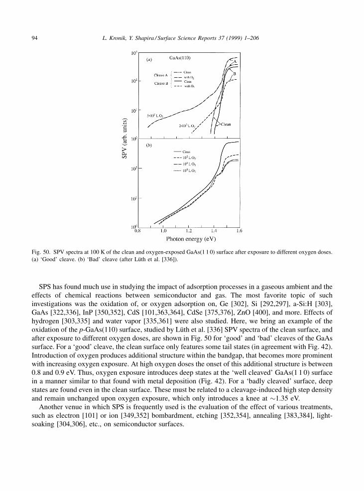
SPS has found much use in studying the impact of adsorption processes in a gaseous ambient and theeffects of chemical reactions between semiconductor and gas. The most favorite topic of suchinvestigations was the oxidation of, or oxygen adsorption on, Ge [302], Si [292,297], a-Si:H [303],GaAs [322,336], InP [350,352], CdS [101,363,364], CdSe [375,376], ZnO [400], and more. Effects ofhydrogen [303,335] and water vapor [335,361] were also studied. Here, we bring an example of theoxidation of the p-GaAs(110) surface, studied by LuÈth et al. [336] SPV spectra of the clean surface, andafter exposure to different oxygen doses, are shown in Fig. 50 for `good' and `bad' cleaves of the GaAssurface. For a `good' cleave, the clean surface only features some tail states (in agreement with Fig. 42).Introduction of oxygen produces additional structure within the bandgap, that becomes more prominentwith increasing oxygen exposure. At high oxygen doses the onset of this additional structure is between0.8 and 0.9 eV. Thus, oxygen exposure introduces deep states at the `well cleaved' GaAs(1 1 0) surfacein a manner similar to that found with metal deposition (Fig. 42). For a `badly cleaved' surface, deepstates are found even in the clean surface. These must be related to a cleavage-induced high step densityand remain unchanged upon oxygen exposure, which only introduces a knee at �1.35 eV.
Another venue in which SPS is frequently used is the evaluation of the effect of various treatments,such as electron [101] or ion [349,352] bombardment, etching [352,354], annealing [383,384], light-soaking [304,306], etc., on semiconductor surfaces.
Fig. 50. SPV spectra at 100 K of the clean and oxygen-exposed GaAs(1 1 0) surface after exposure to different oxygen doses.
(a) `Good' cleave. (b) `Bad' cleave (after LuÈth et al. [336]).
94 L. Kronik, Y. Shapira / Surface Science Reports 37 (1999) 1±206
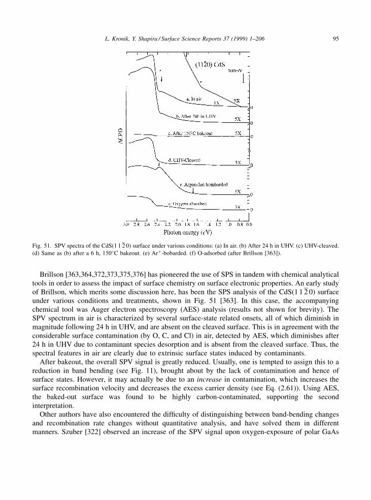
Brillson [363,364,372,373,375,376] has pioneered the use of SPS in tandem with chemical analyticaltools in order to assess the impact of surface chemistry on surface electronic properties. An early studyof Brillson, which merits some discussion here, has been the SPS analysis of the CdS(1 1 2 0) surfaceunder various conditions and treatments, shown in Fig. 51 [363]. In this case, the accompanyingchemical tool was Auger electron spectroscopy (AES) analysis (results not shown for brevity). TheSPV spectrum in air is characterized by several surface-state related onsets, all of which diminish inmagnitude following 24 h in UHV, and are absent on the cleaved surface. This is in agreement with theconsiderable surface contamination (by O, C, and Cl) in air, detected by AES, which diminishes after24 h in UHV due to contaminant species desorption and is absent from the cleaved surface. Thus, thespectral features in air are clearly due to extrinsic surface states induced by contaminants.
After bakeout, the overall SPV signal is greatly reduced. Usually, one is tempted to assign this to areduction in band bending (see Fig. 11), brought about by the lack of contamination and hence ofsurface states. However, it may actually be due to an increase in contamination, which increases thesurface recombination velocity and decreases the excess carrier density (see Eq. (2.61)). Using AES,the baked-out surface was found to be highly carbon-contaminated, supporting the secondinterpretation.
Other authors have also encountered the dif®culty of distinguishing between band-bending changesand recombination rate changes without quantitative analysis, and have solved them in differentmanners. Szuber [322] observed an increase of the SPV signal upon oxygen-exposure of polar GaAs
Fig. 51. SPV spectra of the CdS(1 1 2 0) surface under various conditions: (a) In air. (b) After 24 h in UHV. (c) UHV-cleaved.
(d) Same as (b) after a 6 h, 150�C bakeout. (e) Ar�-bobarded. (f) O-adsorbed (after Brillson [363]).
L. Kronik, Y. Shapira / Surface Science Reports 37 (1999) 1±206 95

surfaces. Here, this increase was assigned to an increase in band-bending since it is very unlikely thatthe additional O-induced states would actually decrease recombination rates. Wang et al. [307] haveobserved an increase in the SPV signal from a-Si:H ®lms after depositing a monolayer of a Langmuir±Blodgett ®lm. Here, the increase was attributed to a decrease in recombination rates because of anincreased relaxation time. Several authors used complementary SPV and PL spectra [344±346,420]. Ifthe increase in SPV was accompanied by an increase in PL, they concluded that this was due to areduction in SRV. This is because the latter increases the SPV and decreases the non-radiativerecombination which competes with the PL. Finally, Kinrot et al. [357] employed complementary time-resolved PL measurements for direct assessment of SRV changes.
Going back to Brillson's experiment, argon bombardment and oxygen adsorption both induce newsurface states, at different energies. The naive interpretation is that these are again extrinsic statesbrought about by the presence of argon or oxygen. However, for argon-ions it was known that nosigni®cant gap states are induced, and the effect of oxygen depended on surface preparation prior tooxidation. AES revealed that for argon bombardment, and at least partially for oxygen adsorption, theextrinsic features were not a direct result of the contaminants. Rather, they were due to a treatment-induced change in surface stoichiometry.
The ability to directly correlate surface electronic structure with chemical treatments may also beused bene®cially in surface passivation studies [348,357]. Such a study on the effect of organic polymeroverlayers on the p-InP(1 0 0) surface, is shown in Fig. 52 [357]. The bare, etched surface displays twoknees, associated with both electron and hole transitions, involving states situated �1.2 eV below theconduction band (`A') and �1.05 eV above the valence band edge (`D'), respectively. These states wereassigned, based on previous SPS studies [352], to excess P and adsorbed O at the surface, respectively.The `A' state is suppressed only in the presence of N-containing polymers, whereas the `D' state issuppressed only by S- or F-containing polymers. This suggests that the surface states are passivated byP±N and (S or F)±O ion exchange processes, respectively.
Fig. 52. SPV spectra of p-InP(1 0 0) surfaces: (a) Etched. (b) Coated with N-containing polymers. (c) Coated with S- or
F-containing polymers (after Kinrot et al. [357]).
96 L. Kronik, Y. Shapira / Surface Science Reports 37 (1999) 1±206

SPS has also been employed for basic studies of surface electronic structure at well-de®ned, cleansurfaces. Several authors have found a correlation between the observed surface states and the surfacestructure. For example, BuÈchel and LuÈth have found that an additional surface state arises whenannealing the Ge(1 1 1)-(2� 1) surface to the (8� 8) con®guration [302]. MoÈnch et al. have found goodagreement between measured and calculated surface states at the Si(0 0 1)-(2�1) surface, supportingthe asymmetric dimer reconstruction model used in the calculations [289]. Clabes and Henzler haveperformed similar studies on the Si(1 1 1) surface [292]. Fig. 53 shows their results for a p-type sample.A distinct difference between surface state energies at the (2� 1) and (7� 7) surface con®gurations isapparent. Oxygen adsorption at the (7� 7) surface greatly changes the SPV spectrum, such thatpositive-SPV-producing transitions to the conduction band are apparent.
Studies of the evolution of metal±semiconductor interfaces using SPS were pioneered by MoÈnchet al. [330] and by Brillson [323,372,373], with later studies being conducted mostly by Shapira et al.[324,352,370] and Musatov et al. [108,338,339,347]. An example is found in Fig. 54, [372] whichfeatures the evolution of SPV spectra of the CdS(1 0 1 0) surface with increasing Au overlayerthickness. While some surface states are already present at the cleaved surface, Au depositionintroduces new surface states. These states vary somewhat with overlayer thickness, before approachinga saturation regime at �7 AÊ . Note that at relatively large Au thickness the signal is lost due toabsorption in the Au layer. An example of a similar SPS study of metals on III±V semiconductors hasalready been given in Fig. 42. These studies, as well as others cited above, provide clear-cutexperimental evidence for the induction of gap states at metal±semiconductor interface by metaldeposition.
In addition to con®rming the existence of interface states, SPS has also been used to understand howthey are formed. A case in point is shown in Fig. 55 [347]. It shows the SPV spectra of the p-InP(1 0 0)surface, thermally cleaned at temperatures below and close to the decomposition temperature of InP, aswell as Pd- and Ag-adsorbed. The striking similarity between the surface states induced by metal
Fig. 53. SPV spectra of the p-type Si(1 1 1) surface for different surface con®gurations (after Clabes and Henzler [292]).
L. Kronik, Y. Shapira / Surface Science Reports 37 (1999) 1±206 97
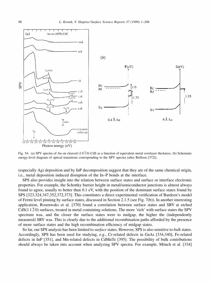
(especially Ag) deposition and by InP decomposition suggest that they are of the same chemical origin,i.e., metal deposition induced disruption of the In±P bonds at the interface.
SPS also provides insight into the relation between surface states and surface or interface electronicproperties. For example, the Schottky barrier height in metal/semiconductor junctions is almost alwaysfound to agree, usually to better than 0.1 eV, with the position of the dominant surface states found bySPS [323,324,347,352,372,373]. This constitutes a direct experimental veri®cation of Bardeen's modelof Fermi level pinning by surface states, discussed in Section 2.1.5 (see Fig. 7(b)). In another interestingapplication, Rosenwaks et al. [370] found a correlation between surface states and SRV at etchedCdS(1 1 2 0) surfaces, treated in metal containing solutions. The more `rich' with surface states the SPVspectrum was, and the closer the surface states were to midgap, the higher the (independentlymeasured) SRV was. This is clearly due to the additional recombination paths afforded by the presenceof more surface states and the high recombination ef®ciency of midgap states.
So far, our SPS analysis has been limited to surface states. However, SPS is also sensitive to bulk states.Accordingly, SPS has been used for studying, e.g., Cr-related defects in GaAs [334,340], Fe-relateddefects in InP [351], and Mn-related defects in CdMnTe [395]. The possibility of bulk contributionsshould always be taken into account when analyzing SPV spectra. For example, MoÈnch et al. [334]
Fig. 54. (a) SPV spectra of Au on cleaved (1 0 1 0) CdS as a function of equivalent metal overlayer thickness. (b) Schematic
energy-level diagram of optical transitions corresponding to the SPV spectra (after Brillson [372]).
98 L. Kronik, Y. Shapira / Surface Science Reports 37 (1999) 1±206

have warned against misinterpreting bulk-defects in GaAs as evidence of surface states at the cleavedGaAs(110) surface. Unfortunately, as already discussed in Section 2.2.3, the simple distinction betweentransitions involving the valence or conduction band based on the sign of the SPV is not valid for bulkstates. Brie¯y, transitions involving bulk states usually decrease the band-bending regardless of theband involved (see Fig. 15) [6]. Under special circumstances, the same bulk transition may contributean either negative or positive knee to the SPV spectrum, depending on the state of the surface charge(see Fig. 17 and the corresponding discussion) [111,113]. The restriction of SPS sign analysis for bulktransitions is not always recognized in the literature and may have led to mis-assignment of statepositions. For example, Simov et al. [362] studied the SPV spectra of polycrystalline CdS thin ®lms.They have observed (among other transitions) the `�1' and `�2' transitions found by Lagowski et al.[361] on single-crystalline CdS, shown in Fig. 49(a), but with the opposite knee sign. They thereforeassumed that the surface states had interacted with the conduction band, rather than with the valenceband. While this may be true, the agreement in observed SPS threshold energies seems striking. Thus, itis also possible that the states observed by Simov et al. were actually located at grain boundaries. Fromthe SPS point of view, these would be `bulk' states as they are not located at the front (free) surface.Thus, the sign of their contribution would be reversed.
The distinction between surface and bulk states is not always an easy task and has attracted someattention in SPS-related research. We defer the discussion of quantitative approaches to such distinctionto Section 5.4.3 and describe some qualitative means here: the most obvious means for distinguishingbetween surface and bulk states is by checking on the sensitivity of the relevant SPV feature to surfacetreatments or to the crystal face studied. SPV features found to `persist' under various conditions[375,377] are attributed to bulk states. Conversely, a marked change upon surface treatment, as in, e.g.,
Fig. 55. SPV spectra of the p-InP(100) surface: (a) Thermally cleaned below the InP decomposition temprature. (b)
Thermally cleaned close to the InP decomposition temprature. (c) After deposition of 0.5 monolayers of Pd. (d) After
deposition of 0.3 monolayers of Ag (after Musatov et al. [347]).
L. Kronik, Y. Shapira / Surface Science Reports 37 (1999) 1±206 99

Figs. 42, 51 or 53, is attributed to surface states. A comparison between contact and contactless SPSmeasurements has also been suggested [294,295] and may be considered as a special case of surfacemodi®cation. In the case of the QD ®lms shown in Fig. 45, the sensitivity of the sub-bandgap spectrumto the ambient suggests a surface state contribution. However, here these states are probably at grainsurfaces and not necessarily at the front surface, as the ®lm is porous. Two pitfalls should be avoidedwhen performing such a distinction: (a) even a bulk transition may be `lost' in the SPV spectra if thesurface is passivated and the band-bending is too low to obtain a meaningful signal. Therefore it isimportant to assess the impact of the surface treatment on the super-bandgap signal as well. (b) asmentioned above, in rare cases, an SPV feature corresponding to a bulk level may `¯ip signs' due tosurface treatment [113]. Sign reversals of the same feature should therefore be treated with caution.Distinction between surface and bulk states has also been performed by means of treating the bulk, e.g.,by changing the bulk dopant [296,340,351,395], or sample fabrication procedures [305,333,393,409].
In the absence of surface or bulk treatments, one of the most popular methods of distinguishingbetween surface and bulk states is comparing SPV and photoconductivity spectra. The latter spectra areinherently insensitive to surface transitions because the photocurrent is collected from the entire bulk ofthe sample, so that the contribution of the SCR is typically negligible. Therefore, transitions appearingin both types of spectra are usually attributed to bulk transitions, whereas transitions appearing in theSPV spectra alone are assigned to surface states. In fact, the lack of correlation betweenphotoconductivity and SPV spectra was used as proof of observing `true' surface phenomena in theearliest days of SPS, as shown in Fig. 49. A more comprehensive example, measured at Si-doped GaAsepitaxial thin ®lms, where three bulk states (`E1'±`E3') and two surface states (`Et4', `Et5') are found, isshown in Fig. 56 [337]. The `l series' and `n series' phonons in Fig. 47 were identi®ed as bulk andsurface phonons, respectively, using a similar comparison with photoconductivity. More examples ofuse of this procedure may be found in, e.g., [319,334,360,365,366,371,375,386,407].
While very useful, photoconductivity is not fail-safe: Vyvenko et al. [371] have used SPS to point outa misinterpretation of photoconductivity data of CdS:Te crystals. They noted that the bandgap-relatedfeature found in SPS is completely absent in the photoconductivity spectrum, due to the unusually largeabsorption coef®cient which reduces the photoconducting layer. Therefore, the energy previouslyassigned to the bandgap was actually related to a bulk defect. Szaro [377] has found an SPS featurewhich behaved as a bulk state in the sense that it persisted through various surface treatments andorientations, but was not apparent in photoconductivity nevertheless. The reason for the discrepancy isnot clear. Another case worth mentioning is the studies of a-Si:H, with and without H2 dilution,performed by Fefer et al. [305], which is shown in Fig. 57. Based on the agreement between the SPSresults and the constant photocurrent method, on the sensitivity of the spectra to bulk treatment evidentin the ®gure, and on the agreement with theoretical models, the transitions observed have been assignedto bulk states. Nevertheless, agreement with theoretical models is only established when using signconventions appropriate for surface states. Therefore, it was assumed that the surface has a defectstructure similar to the bulk in this case, which is reasonable for an amorphous material.
In Fig. 57, an increase of both the bandgap-related SPV (at �1.7 eV) and the gap-state-related SPV(at �1.1±1.2 eV) upon H2 dilution is observed. This is not coincidental, as gap states associated withthe band with which they communicate typically feature the same dependence as the bandgap energyon the bandgap-modulating parameter. Using this idea in a systematic manner, a correlation betweengap states and bands was found in CdTe [387] and CdMnTe [388] via temperature-induced bandgapchanges, and in InAlAs thin ®lms [355] via alloy-composition-induced bandgap changes. In the latter
100 L. Kronik, Y. Shapira / Surface Science Reports 37 (1999) 1±206
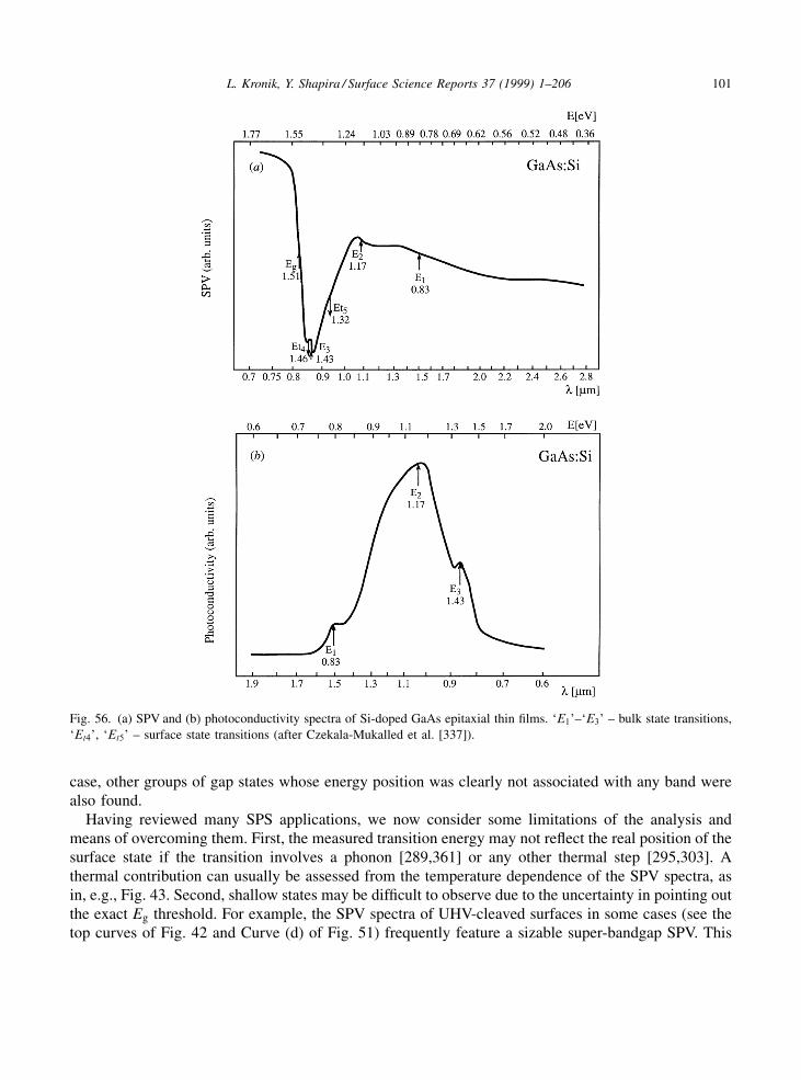
case, other groups of gap states whose energy position was clearly not associated with any band werealso found.
Having reviewed many SPS applications, we now consider some limitations of the analysis andmeans of overcoming them. First, the measured transition energy may not re¯ect the real position of thesurface state if the transition involves a phonon [289,361] or any other thermal step [295,303]. Athermal contribution can usually be assessed from the temperature dependence of the SPV spectra, asin, e.g., Fig. 43. Second, shallow states may be dif®cult to observe due to the uncertainty in pointing outthe exact Eg threshold. For example, the SPV spectra of UHV-cleaved surfaces in some cases (see thetop curves of Fig. 42 and Curve (d) of Fig. 51) frequently feature a sizable super-bandgap SPV. This
Fig. 56. (a) SPV and (b) photoconductivity spectra of Si-doped GaAs epitaxial thin ®lms. `E1'±`E3' ± bulk state transitions,
`Et4', `Et5' ± surface state transitions (after Czekala-Mukalled et al. [337]).
L. Kronik, Y. Shapira / Surface Science Reports 37 (1999) 1±206 101
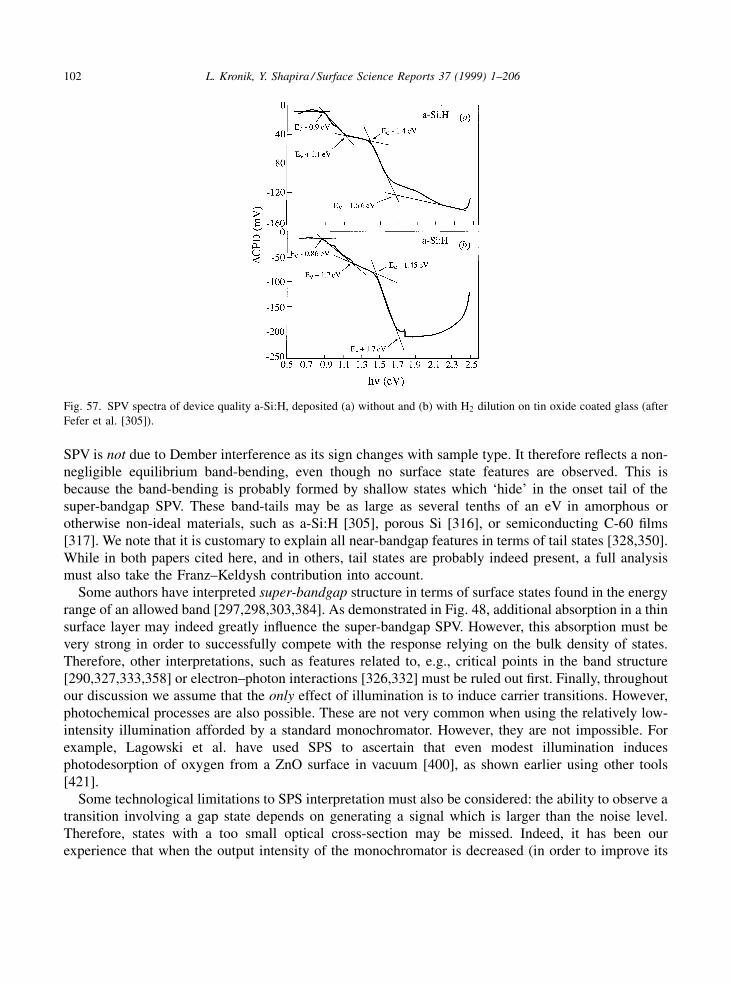
SPV is not due to Dember interference as its sign changes with sample type. It therefore re¯ects a non-negligible equilibrium band-bending, even though no surface state features are observed. This isbecause the band-bending is probably formed by shallow states which `hide' in the onset tail of thesuper-bandgap SPV. These band-tails may be as large as several tenths of an eV in amorphous orotherwise non-ideal materials, such as a-Si:H [305], porous Si [316], or semiconducting C-60 ®lms[317]. We note that it is customary to explain all near-bandgap features in terms of tail states [328,350].While in both papers cited here, and in others, tail states are probably indeed present, a full analysismust also take the Franz±Keldysh contribution into account.
Some authors have interpreted super-bandgap structure in terms of surface states found in the energyrange of an allowed band [297,298,303,384]. As demonstrated in Fig. 48, additional absorption in a thinsurface layer may indeed greatly in¯uence the super-bandgap SPV. However, this absorption must bevery strong in order to successfully compete with the response relying on the bulk density of states.Therefore, other interpretations, such as features related to, e.g., critical points in the band structure[290,327,333,358] or electron±photon interactions [326,332] must be ruled out ®rst. Finally, throughoutour discussion we assume that the only effect of illumination is to induce carrier transitions. However,photochemical processes are also possible. These are not very common when using the relatively low-intensity illumination afforded by a standard monochromator. However, they are not impossible. Forexample, Lagowski et al. have used SPS to ascertain that even modest illumination inducesphotodesorption of oxygen from a ZnO surface in vacuum [400], as shown earlier using other tools[421].
Some technological limitations to SPS interpretation must also be considered: the ability to observe atransition involving a gap state depends on generating a signal which is larger than the noise level.Therefore, states with a too small optical cross-section may be missed. Indeed, it has been ourexperience that when the output intensity of the monochromator is decreased (in order to improve its
Fig. 57. SPV spectra of device quality a-Si:H, deposited (a) without and (b) with H2 dilution on tin oxide coated glass (after
Fefer et al. [305]).
102 L. Kronik, Y. Shapira / Surface Science Reports 37 (1999) 1±206

energy resolution) some of the weaker features may disappear (a recent example may be found in[318]). As shown in Section 2.2.3, the SPV signal decreases with decreasing semiconductor bandgapand surface band-bending. Thus, sub-bandgap features are more likely to be missed in relatively smallbandgap materials and/or reasonably passivated surfaces. For example, Tong and Lam [105] failed toobserve any sub-bandgap signals related to the Si±SiO2 interface, even though the existence of gapstates at that interface is well-known from, e.g., electrical measurements. They then con®rmedtheoretically that for reasonable interface state parameters, the SPV signal is indeed expected to besmaller than the noise level.
An associated problem is that the energy at which the onset of a certain transition is identi®ed mayactually be larger than the real threshold, re¯ecting only the energy at which the SPV change inducedby this transition exceeds the noise level. The identi®cation of the lowest-energy threshold may beparticularly dif®cult when using a logarithmic representation. As long as the SPV curve approaches avertical asymptote, as in, e.g., Fig. 53, this asymptote obviously re¯ects the energy threshold. However,if the asymptote is not vertical, as in, e.g., Fig. 50, the energy threshold is not obvious.
As demonstrated in Fig. 16, the sub-bandgap SPV increases with increasing equilibrium bandbending in a manner similar (though not identical) to that of super-bandgap SPV. Therefore, smalldecreases in surface-state position upon increasing metal coverage (e.g., the change between 1.75 and1.74 eV in Fig. 54) may actually re¯ect the improving SNR due to an increasing band-bending, ratherthan a true shift in energy position. Similar, but larger (as much as 0.1 eV) pseudo-shifts have beenidenti®ed by Burstein et al. [324]. A shift of threshold energies has also been observed whenperforming SPS as a function of external bias in a MIS arrangement [291]. Note that increases inthreshold energies for larger Au coverages in Fig. 54 do re¯ect physical changes as the equilibriumband-bending, which increases with increasing Au coverage, can only decrease the threshold energy.
The problems associated with determining state transition energies by inspection may becircumvented by an extrapolation which is very similar to that suggested for determining Eg. As insuper-bandgap illumination, sub-bandgap illumination is also expected to reasonably re¯ect theabsorption spectrum for suf®ciently low illumination [289,293,374]. Accordingly, assuming a discretesurface state the SPV intensity should re¯ect the photon-energy dependence of the optical cross-section.The above-threshold SPV may therefore be ®tted with an exponential dependence, or other functionalforms deemed relevant (see Eq. (2.84)), and extrapolated to zero to ®nd the threshold energy[101,108,289]. Using this approach, Musatov et al. [108,338,339] have studied the coveragedependence of metal-induced surface states. They have found that in many cases the energy positionof the induced states is ®xed, but in some cases it varies with coverage. Such a change probably re¯ectsa change in the physical/chemical origin of the state at some thickness.
One obvious possibility of improving the SNR is increasing the illumination intensity. Whileoptimizing the illumination source has been shown to have some success in resolving extra features[390], the improvement obtained is limited. Increasing the band-bending via an external dc bias in aMIS arrangement also improves the SNR. A different approach relies on lowering the measurementtemperature [298,386], which suppresses thermally-induced transitions and hence increases both thesuper- and sub-bandgap SPV (see Section 2). An example is shown in Fig. 58(a) [395], which showsSPV spectra of unintentionally doped CdMnTe at various temperatures. At room temperature, the onsetof the sub-bandgap SPV seems to be at �0.9 mm, whereas at lower temperatures it is clear that the onsetis much deeper (at �1.5 mm), and was obscured by the noise level at room temperature. This featurewas found to be correlated to Mn-induced bulk states. Unfortunately, the SPV spectra do not always
L. Kronik, Y. Shapira / Surface Science Reports 37 (1999) 1±206 103
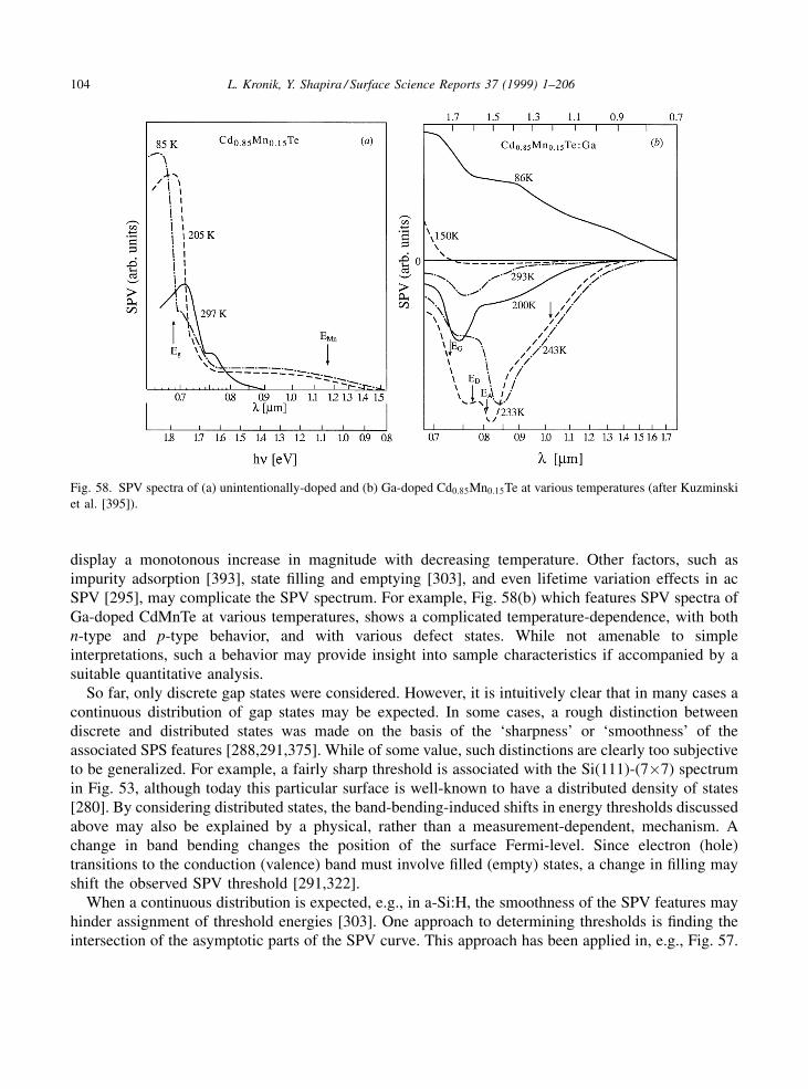
display a monotonous increase in magnitude with decreasing temperature. Other factors, such asimpurity adsorption [393], state ®lling and emptying [303], and even lifetime variation effects in acSPV [295], may complicate the SPV spectrum. For example, Fig. 58(b) which features SPV spectra ofGa-doped CdMnTe at various temperatures, shows a complicated temperature-dependence, with bothn-type and p-type behavior, and with various defect states. While not amenable to simpleinterpretations, such a behavior may provide insight into sample characteristics if accompanied by asuitable quantitative analysis.
So far, only discrete gap states were considered. However, it is intuitively clear that in many cases acontinuous distribution of gap states may be expected. In some cases, a rough distinction betweendiscrete and distributed states was made on the basis of the `sharpness' or `smoothness' of theassociated SPS features [288,291,375]. While of some value, such distinctions are clearly too subjectiveto be generalized. For example, a fairly sharp threshold is associated with the Si(111)-(7�7) spectrumin Fig. 53, although today this particular surface is well-known to have a distributed density of states[280]. By considering distributed states, the band-bending-induced shifts in energy thresholds discussedabove may also be explained by a physical, rather than a measurement-dependent, mechanism. Achange in band bending changes the position of the surface Fermi-level. Since electron (hole)transitions to the conduction (valence) band must involve ®lled (empty) states, a change in ®lling mayshift the observed SPV threshold [291,322].
When a continuous distribution is expected, e.g., in a-Si:H, the smoothness of the SPV features mayhinder assignment of threshold energies [303]. One approach to determining thresholds is ®nding theintersection of the asymptotic parts of the SPV curve. This approach has been applied in, e.g., Fig. 57.
Fig. 58. SPV spectra of (a) unintentionally-doped and (b) Ga-doped Cd0:85Mn0:15Te at various temperatures (after Kuzminski
et al. [395]).
104 L. Kronik, Y. Shapira / Surface Science Reports 37 (1999) 1±206
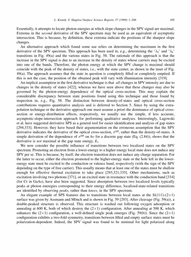
Essentially, it attempts to locate photon energies at which slope changes in the SPV signal are maximal.Extrema in the second derivative of the SPV spectrum may be used as an equivalent of asymptoticintersection. This is because, by de®nition, these extrema indicate the positions of the sharpest slopechanges.
An alternative approach which found some use relies on determining the maximum in the ®rstderivative of the SPV spectrum. This approach has been used in, e.g., determining the `�4' and `�6'transitions in Fig. 49(a) and the various states in Fig. 58. The rationale of this approach is that theincrease in the SPV signal is due to an increase in the density of states whose carriers may be excitedinto one of the bands. Therefore, the photon energy at which the SPV change is maximal shouldcoincide with the peak of the density of states, i.e., with the state center, as shown in the inset of Fig.49(a). The approach assumes that the state in question is completely ®lled or completely emptied. Ifthis is not the case, the position of the obtained peak will vary with illumination intensity [319].
An implicit assumption in the ®rst derivative technique is that all changes in SPV intensity are due tochanges in the density of states [422], whereas we have seen above that these changes may also begoverned by the photon-energy dependence of the optical cross-section. This may explain theconsiderable discrepancy between state positions found using this technique and those found byinspection in, e.g., Fig. 58. The distinction between density-of-states and optical cross-sectioncontributions requires quantitative analysis and is deferred to Section 5. Since by using the extra-polation technique or the derivative approach one must assume a priori the dominance of optical cross-section or energy-distribution effects, respectively, we usually use the simple, if less accurate,asymptotic-slope-intersection approach for performing qualitative analyses. Interestingly, Lagowskiet al. have suggested derivative SPS as a general tool for easier identi®cation and analysis of gap states[294,333]. However, they have based their argumentation on the erroneous assumption that the SPVderivative indicates the derivative of the optical cross-section, �opt, rather than the density-of-states. Asimple derivation of the dependence of �opt on h� for a discrete gap state (Eq. (2.84)), shows that thederivative is not maximal at the gap state energy, Et.
We now consider the possible in¯uence of transitions between two localized states on the SPVspectrum. Promoting an electron from a lower-energy to a higher energy local state does not induce anySPV per se. This is because, by itself, the electron transition does not induce any charge separation. Forthe latter to occur, either the electron promoted to the higher-energy state or the hole left in the lower-energy state must be excited to the conduction or valence band, respectively (with the sign of the SPVdepending on the type of free carrier). This usually means that at least one of the states must be shallowenough for effective thermal excitation to take place [293,321,335]. Other mechanisms, such asexcitation involving two photons [371], or an excited state in resonance with the conduction band [334](for Cr in GaAs), have also been suggested. Since absorption between two localized levels typicallypeaks at photon eneregies corresponding to their energy difference, localized-state-related transitionsare identi®ed by observing peaks, rather than knees, in the SPV spectrum.
An elegant example of SPS features due to transitions between local states at the Si(111)-(2�1)surface was given by Assmann and M�oÈnch and is shown in Fig. 59 [293]. After cleavage (Fig. 59(a)), adouble-peaked structure is observed. This structure is washed out following oxygen adsorption orannealing at 600 K, both of which destroy the (2�1) con®guration. After annealing at 500 K, whichenhances the (2�1) con®guration, a well-de®ned single peak emerges (Fig. 59(b)). Since the (2�1)con®guration exhibits a two-fold symmetry, transitions between ®lled and empty surface states must bepolarization-dependent. Indeed, the SPV signal was found to be minimal for light polarized along
L. Kronik, Y. Shapira / Surface Science Reports 37 (1999) 1±206 105

(1 1 0) directions and maximal for light polarized along (1 1 2) directions. The observed peak wastherefore interpreted as arising from transitions between ®lled and empty bond states, localized atalternate rows of raised and depressed atoms, respectively, running along a (1 1 0) direction.
4.3. Points of importance
In this section, we point out a number of important elements, related to the measurement conditions,that must be taken into account in order to obtain meaningful SPS data.
We have assumed so far that thermal equilibrium is always established between the surface and bulkin the dark. However, this is not necessarily true since the relaxation times of excited samples may be aslong as several days if the surface barrier is much larger than the thermal energy. At room temperature,this phenomena has been observed primarily for high bandgap samples [6,360,361]. At lowtemperature, it has been observed in a-Si:H [303], in plastically deformed Si and Ge [419], and even incrystalline Si [298]. Evidence of SPS performed in the absence of thermal equilibrium prior toillumination may be found in, e.g., Fig. 49, where transitions with both bands involving the same surfacestate were obtained. States which are well removed from the surface Fermi level (as is the case here) areexpected to be completely ®lled or completely empty in equilibrium. Therefore, only electron or holetransitions, respectively, are expected. The observation of both transitions indicates a partial ®lling ofthe state involved, and hence non-equilibrium conditions. Similar effects have also been encountered byother groups [386,393,397]. Goldstein and Szostak measured a-Si:H samples at low temperatures [303].They reported a lack of relaxation so severe that the sample had to be re-heated and than cooled downagain after each data point on the spectrum to allow thermal equilibrium conditions to develop.
Due to different initial surface conditions, SPV spectra taken after equilibrium and non-equilibriumconditions in the dark may differ drastically. Moreover, many quantitative analyses, which assumethermal equilibrium in the dark, would yield erroneous information when applied to measurements inwhich this assumption is not valid. For obtaining unequivocal measurements, it is thus very important
Fig. 59. SPV spectra of a Si(1 1 1)-(2�1) surface: (a) After cleavage and following exposure to O2 at 300 K. (b) After
cleavage and following 10 min annealing at 500 K (after Assmann and MoÈnch [293]).
106 L. Kronik, Y. Shapira / Surface Science Reports 37 (1999) 1±206

to let the sample relax for a suf®cient time in complete darkness. When working with a Kelvin probe, itis possible to ascertain that the sample has relaxed by monitoring the CPD in the dark as a function oftime. We caution that a casual reading of a seemingly stable CPD does not suf®ce, as the relaxationtimes involved may be extremely long.
Varying the initial surface conditions by deliberately avoiding thermal equilibrium in the dark maybe advantageous if proper adjustments to any interpretations are made. For example, Gatos andLagowski [6] have compared between the SPV spectra of ZnO basal surfaces measured 1 h and 24 hafter illumination with white light, as shown in Fig. 60. The completely different spectra may beinterpreted as follows: after 24 h, thermal equilibrium is approximately established, the observedsurface state is ®lled with electrons, and electron transitions from the state to the conduction band areobserved. However, 1 h after illumination thermal equilibrium has not been established yet, the samesurface state is empty, and hole transitions to the valence band are observed. This is supported by notingthat the sum of the two corresponding transition energies is very nearly equal to the ZnO bandgap. In adifferent example, Yang et al. [301] have compared SPV spectra taken after different initial conditions(illumination and bias) in order to con®rm photo-memory effects in Langmuir±Blodgett ®lms capping aSi sample.
When using dc SPV, it is equally important to ascertain that steady-state conditions have indeed beenreached following illumination since response times may also be very long if, e.g., `slow' surface statesare involved. It is therefore strongly recommended to make sure that suf®cient time is allowed at eachphoton energy for steady-state to be obtained, which can be examined by checking for an in¯uence ofvariations in the monochromator dwell time at each wavelength on the obtained spectrum. This hasrecently been demonstrated by Shalish et al. [360], who used SPS to study GaN ®lms, as shown in
Fig. 60. SPV spectra of the basal ZnO surface in room temperature and ambient, (a) 1 h and (b) 24 h after illumination with
white light. Insets represent the dominant transitions involved (after Gatos and Lagowski [6]).
L. Kronik, Y. Shapira / Surface Science Reports 37 (1999) 1±206 107

Fig. 61. As the dwell time at each measurement point increases, the sub-bandgap SPV signal increasesand more gap-state related features are exposed. Many of these features would have been overlookedhad the SPV spectrum at the shorter dwell time been mistaken for a steady-state one. We note thatappropriate dwell times should be sought with particular caution at wavelengths in which ®lters orgratings are exchanged because the disruption from the previous steady-state conditions may be moresigni®cant at such points. In addition, light may reach the sample during these changes and cause anadditional undesirable excitation which must be allowed to relax before resuming the measurement.
When long response-time transitions are involved, their corresponding SPV features are likely to goundetected when using ac SPV because the illumination chopping rate may be too fast to allow anynon-negligible population changes in the `slow' states involved [100,110,321,386]. In fact, Gatos et al.[6] have been able to advance SPS much more than other early researchers [100,239] partly becausethey used dc, rather than ac, spectroscopy, thereby revealing a set of surface states not previouslyexposed. The lack of sensitivity of ac SPV to slow states has also been used bene®cially. The presenceof some spectral features in dc, but not ac, SPV, has been used to conclude that the observed featuresare related to surface, rather than bulk, states [6,386,393,394]. While this method has been used withsome success, it is in fact quite limited because it assumes that bulk states are invariably fast andsurface states are invariably slow, which is not always true.
Even if steady-state conditions have been ascertained, it is always a good idea to examine the detailsof the transient SPV response as well. This point has been elegantly demonstrated by Morawski et al.[321], who studied etched GaAs surfaces. A comparison between ac and dc SPS (Fig. 62(a)) revealsthat the two spectroscopies converge for super-bandgap illumination, but the SPV signal is muchgreater in dc SPS. The difference in magnitudes con®rms that steady-state conditions have not beenobtained in ac SPV. While the shape of the spectra is also somewhat different, no immediately evidentmajor difference in spectral features is noted. The transient response (Fig. 62(b)) reveals that the SPVsignal is composed of a slow and a fast component. Whereas ac SPV only shows the latter, steady-statedc SPV shows the sum of both components, so that the slow state is never explicitly presented. If themagnitude of the two processes is independently plotted versus photon energy (Fig. 62(c)), it becomesclear that two physical mechanisms, and not one, have been monitored: The fast state, which has a`knee' shape, is related to a state-band transition, whereas the slow component, which has a `peak'shape, is related to transitions between two localized levels.
Fig. 61. SPV spectra of a GaN ®lm at different monochromator dwell times (after Shalish et al. [360]).
108 L. Kronik, Y. Shapira / Surface Science Reports 37 (1999) 1±206
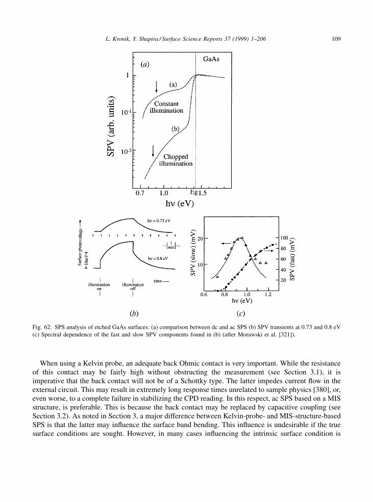
When using a Kelvin probe, an adequate back Ohmic contact is very important. While the resistanceof this contact may be fairly high without obstructing the measurement (see Section 3.1), it isimperative that the back contact will not be of a Schottky type. The latter impedes current ¯ow in theexternal circuit. This may result in extremely long response times unrelated to sample physics [380], or,even worse, to a complete failure in stabilizing the CPD reading. In this respect, ac SPS based on a MISstructure, is preferable. This is because the back contact may be replaced by capacitive coupling (seeSection 3.2). As noted in Section 3, a major difference between Kelvin-probe- and MIS-structure-basedSPS is that the latter may in¯uence the surface band bending. This in¯uence is undesirable if the truesurface conditions are sought. However, in many cases in¯uencing the intrinsic surface condition is
Fig. 62. SPS analysis of etched GaAs surfaces: (a) comparison between dc and ac SPS (b) SPV transients at 0.73 and 0.8 eV
(c) Spectral dependence of the fast and slow SPV components found in (b) (after Morawski et al. [321]).
L. Kronik, Y. Shapira / Surface Science Reports 37 (1999) 1±206 109

desired since the band-bending can be increased, thereby increasing SPS sensitivity. Moreover, using aMIS structure, the surface band-bending may be systematically changed by means of an external dcbias. This additional degree of freedom may assist in uncovering and characterizing further gap states[291,405]. We note that several groups have employed SPS principles with contact measurements ± viaan electrolyte [354], a metallic contact [294,295,313,407], or a transparent conductor [307,314,315,369]. Obviously, the effect of the contact on surface properties must be particularly considered insuch cases.
An issue of great importance is the possible variation of photon ¯ux with photon energy. In aconventional monochromator, the photon ¯ux exhibits a rather signi®cant spectral dependence (at timesover several orders of magnitude) and only recently has a systematic SPS setup with a constant photon¯ux been demonstrated [423]. The variations in photon ¯ux may introduce bogus features in SPVspectra, which re¯ect nothing but changes in the excitation level [417]. It is therefore a standard andwidely used procedure to normalize all spectra by dividing the SPV signal by the photon ¯ux ateach photon energy. Unfortunately, this procedure is clearly unjusti®ed since the dependence ofthe SPV on the photon ¯ux may be highly non-linear! Such normalization is strictly forbidden,unless a linearity between the SPV and photon ¯ux has been deomnstrated in the entire spectral rangestudied.
If the SPV is not linear in the photon ¯ux, it seems natural to normalize the SPV based on its exactintensity-dependence. However, this procedure is cumbersome since the intensity-dependence in somespectral regions may differ. BuÈchel and LuÈth [302] have therefore studied the intensity-dependence oftwo representative photon energies ± one at a sub-bandgap energy and the other at a super-bandgapenergy ± and normalized the two portions of the spectrum independently. While this approach was amajor step in the right direction, it has not been in much use, because it requires many extrameasurements. Moreover, the intensity dependence may vary in different regions inside the sub- orsuper-bandgap regimes, so that normalization by two photon energies is not necessarily suf®cient.Another mistake sometimes made is confusing time- and intensity-saturation [350], i.e., assuming thatat steady-state the dependence on illumination intensity is negligible. In light of the analysis in Section 2and in this section, this is clearly wrong, unless recombination rates are negligible.
If a constant photon ¯ux or a proper SPV normalization procedure are not attainable, it is best not toperform any manipulation on the as-measured spectrum as this may corrupt the data. Instead, the SPVspectrum should be compared with the spectral features of the light source to check for suspectedartifacts. For example, the feature at �1.18 eV in Fig. 52 is simply due to a change of ®lter at thatenergy. When in doubt, comparing between spectra obtained using different gratings or different ®lter-exchange energies usually provides a clear-cut distinction between photon-¯ux-induced artifacts andreal features.
Finally, as in any spectroscopy, removal of stray light is crucial for increasing the energy resolutionand avoiding artifacts due to second-order re¯ections of monochromator gratings. In SPS, it isparticularly important to consider stray-light effects in the vicinity of the bandgap energy. Since theabsorption coef®cient drastically increases around this energy, even a small number of stray photonswith higher energies may produce a signi®cant stray signal. This is an additional, measurement-dependent reason, for the broad onset of the super-bandgap signal discussed in Section 4.1. Therefore,it is extremely important to rule out stray light effects (or at least to assess their magnitude) beforeinterpreting the near-bandgap signal in terms of physical effects, e.g., tail-states and/or the Franz±Keldysh effect.
110 L. Kronik, Y. Shapira / Surface Science Reports 37 (1999) 1±206
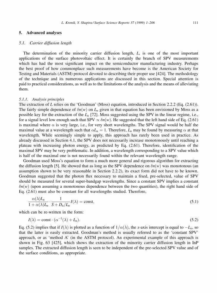
5. Advanced analyses
5.1. Carrier diffusion length
The determination of the minority carrier diffusion length, L, is one of the most importantapplications of the surface photovoltaic effect. It is certainly the branch of SPV measurementswhich has had the most signi®cant impact on the semiconductor manufacturing industry. Perhapsthe best proof of how commonplace such measurements have become is the American Society forTesting and Materials (ASTM) protocol devoted to describing their proper use [424]. The methodologyof the technique and its numerous applications are discussed in this section. Special attention ispaid to practical considerations, as well as to the limitations of the analysis and the means of alleviatingthem.
5.1.1. Analysis principles
The extraction of L relies on the `Goodman' (Moss) equation, introduced in Section 2.2.2 (Eq. (2.61)).The fairly simple dependence of �n�w� on Ln given in that equation has been envisioned by Moss as apossible key for the extraction of the Ln [72]. Moss suggested using the SPV in the linear regime, i.e.,for a signal level low enough such that SPV / �n�w�. He suggested that the left hand side of Eq. (2.61)is maximal where � is very large, i.e., for very short wavelengths. The SPV signal would be half themaximal value at a wavelength such that �Ln � 1. Therefore, Ln may be found by measuring � at thatwavelength. While seemingly simple to apply, this approach has rarely been used in practice. Asalready discussed in Section 4.1, the SPV does not necessarily increase monotonously until reaching aplateau with increasing photon energy, as predicted by Eq. (2.61). Therefore, identi®cation of themaximal SPV may be very problematic. In addition, a wavelength corresponding to a SPV value whichis half of the maximal one is not necessarily found within the relevant wavelength range.
Goodman used Moss's equation to form a much more general and rigorous algorithm for extractingthe diffusion length [5]. He showed that as long as the SPV dependence on �n�w� was monotonous (anassumption shown to be very reasonable in Section 2.2.2), its exact form did not have to be known.Goodman suggested that the photon ¯ux necessary to maintain a ®xed, pre-selected, value of SPVshould be measured for several super-bandgap wavelengths. Since a constant SPV implies a constant�n�w� (upon assuming a monotonous dependence between the two quantities), the right hand side ofEq. (2.61) must also be constant for all wavelengths studied. Therefore,
����Ln
1� ����Ln
� 1
S� Dn=Ln
I��� � const; (5.1)
which can be re-written in the form:
I��� � const � ��ÿ1��� � Ln�: (5.2)
Eq. (5.2) implies that if I��� is plotted as a function of 1=����, the x-axis intercept is equal to ÿLn, sothat the latter is easily extracted. Goodman's method is usually referred to as the `constant SPV'approach, or as `method A' (in the ASTM protocol). An experimental example of this approach isshown in Fig. 63 [425], which shows the extraction of the minority carrier diffusion length in InPsamples. The extracted diffusion length is seen to be independent of the pre-selected SPV value and ofthe surface conditions, as appropriate.
L. Kronik, Y. Shapira / Surface Science Reports 37 (1999) 1±206 111

A modi®cation of Goodman's approach, usually referred to as the `linear SPV' approach or as`Method B', relies on measuring the SPV in the linear regime. Using this linearity in Eq. (2.61) yields:
I���SPV��� � const � 1� �Ln
�Ln
� const � ��ÿ1��� � Ln�: (5.3)
Eq. (5.3) suggests that in the linear SPV regime, Ln may be extracted using a linear plot very similar tothat shown in Fig. 63, except that the y-axis is I���=SPV���, rather than I��� which maintains aconstant SPV. This method is usually attributed to Quilliet and Gosar [426]. However, while theseauthors did suggest using the SPV in the linear regime, they did not suggest using an extrapolationscheme based on Eq. (5.3). Rather, they extracted Ln from the slope of a SPV=� versus � curve.
Using SPV to extract the minority carrier diffusion length has two distinct advantages over othertechniques: First, the method presented here is a steady-state method. As a result, it is immune to timeconstants which combine bulk and surface processes ± a major limitation of methods such asphotoconductive decay (PCD) [427]. Surface recombination processes affect the SPV method only viaS, the surface recombination velocity. As can be judged by either Eq. (5.1) or Fig. 63, changes in S canchange the SPV magnitude as well as the slope of the linear curve used to extract Ln, but not theintercept (and hence extracted Ln) value. The second advantage of the SPV technique is that it may beused in a contactless manner and that it is cheaper and more simple in both operation and interpretationthan other contactless methods, e.g., microwave PCD (�PCD) [428,429]. The SPV technique is alsoeasy to use due to the availability of an ASTM protocol. In addition, it is readily amenable to operationin a scanning mode, as ®rst demonstrated by Lile [427] and followed by many others in variousapplications [431±438].
Despite its numerous advantages, the acceptance of the SPV technique as a main-stream diffusionlength measurement tool did not happen at once. While used successfully by other groups shortly afterits initial introduction [439,440], the technique has largely lay dormant. In fact, in the 15 years after thepioneering work performed in the early 1960s [5,426], only a handful of additional articles which used
Fig. 63. Photon ¯ux vs. the inverse absorption coef®cient, �ÿ1, of (100) InP samples, for several SPV values. circles ± sample
with a relatively low SRV, crosses ± sample with a relatively high SRV (after Li [425]).
112 L. Kronik, Y. Shapira / Surface Science Reports 37 (1999) 1±206
the technique and/or developed it further have been published [425,427,441±443]. The ®rst community,which seriously embraced the SPV approach, starting in the mid-1970s, was the solar cell community[433,434,443±451]. This is because the minority carrier diffusion length is one of the most importantparameters which control the conversion ef®ciency of solar cell devices [452]. Following the success ofthese early SPV measurements in the evaluation of solar energy materials, the technique has become astandard tool of solar-cell research. Some relatively recent applications may be found in [435,436,453±463]. Speci®cally, throughout the 1980s and early 1990s, much attention has been devoted to a-Si:H.These studies were pioneered by Dresner, Goldstein, and Szostak [464], and were followed by manyother research groups [304,465±485]. Measurements of a-Si:H are presented in Section 5.1.3 as part ofthe discussion of the limitations of the SPV approach.
The second area where SPV-based diffusion length measurements have become very popular,especially in recent years, is the monitoring of Si wafers for the semiconductor industry. Here, theminority carrier diffusion length is used as a sensitive tool for observing contamination and/or defectswhich serve as charge recombination centers. As in the case of solar cells, the technique did not becomewide-spread for many years. Despite early successful applications of the approach to single-crystal Si[426,427,439] and the emergence of the ®rst ASTM protocol in 1978, no sustained effort of using SPVfor Si wafers has been undertaken. In 1983, it was up to Goodman himself to show that SPV-monitoringcan successfully detect various contamination sources, such as loading stations in ion implanters,boron-doping sources, and inadequate wafer cleaning and handling [486]. Goodman et al. havespeci®cally lamented the under-utilization of SPV tools in the Si industry in general and incontamination monitoring in particular [486]. Nevertheless, use of such tools remained sporadic at bestthroughout most of the 1980s (see [486,487], and references therein).
The situation changed dramatically towards the end of the 1980s. Within a few years, the importanceof SPV tools had risen dramatically, mostly due to a fortunate coincidence of two major developments,designed to answer the increasing needs of the Si industry.
In the ®rst development, Lagowski et al. have designed and commercialized [232] a computerized,scanning, contactless SPV machine (already shown in Fig. 29) [12]. By speci®cally targeting the Siindustry, both in terms of developing tools suitable for an industrial environment and in terms ofaggressively exposing the new tools to the relevant community, these scientists have contributed to thepromotion of SPV methods considerably. Today, their SPV equipment, as well as that of others [233] isextensively used for both industrial monitoring and research applications.
The second development is related to the increasing importance of metal impurities. Speci®cally, Feis known to be a problematic metallic impurity since it is a main constituent of many importantmaterials and a common impurity in chemicals [488]. Moreover, due to its high solubility and fastdiffusivity at elevated temperatures, Fe is easily introduced in the IC fabrication environment [489]. Fecontamination has been found to increase leakage currents [487,490] and decrease the breakdownvoltage [12,491,492] and the radiation hardness [490] in MOS-based integrated circuits. It has alsobeen found to degrade bipolar transistor performance [12,493] and decrease the breakdown voltage ofpower devices [494]. The more advanced the Si manufacturing technology is, the more severecontamination effects become. Ultra-large-scale integrated Si circuits are particularly vulnerable todetrimental effects of contamination on their performance, due to smaller device geometries, shallowerjunctions, decreased gate oxide thickness, and larger chip areas [12,488,491].
An elegant solution for the increasing need of an accurate, non-destructive, monitoring of the Feconcentration in B-doped Si wafers, based on SPV diffusion length measurements, has been forwarded
L. Kronik, Y. Shapira / Surface Science Reports 37 (1999) 1±206 113
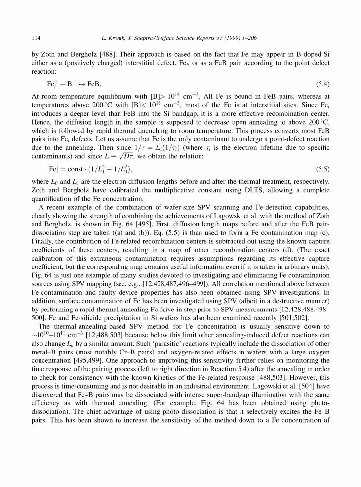
by Zoth and Bergholz [488]. Their approach is based on the fact that Fe may appear in B-doped Sieither as a (positively charged) interstitial defect, Fei, or as a FeB pair, according to the point defectreaction:
Fe�i � Bÿ $ FeB: (5.4)
At room temperature equilibrium with [B]> 1014 cmÿ3, All Fe is bound in FeB pairs, whereas attemperatures above 200 �C with [B]< 1016 cmÿ3, most of the Fe is at interstitial sites. Since Fei
introduces a deeper level than FeB into the Si bandgap, it is a more effective recombination center.Hence, the diffusion length in the sample is supposed to decrease upon annealing to above 200 �C,which is followed by rapid thermal quenching to room temperature. This process converts most FeBpairs into Fei defects. Let us assume that Fe is the only contaminant to undergo a point-defect reactiondue to the annealing. Then since 1=� � �i�1=�i� (where �i is the electron lifetime due to speci®ccontaminants) and since L � ������
D�p
, we obtain the relation:
�Fe� � const � �1=L21 ÿ 1=L2
0�; (5.5)
where L0 and L1 are the electron diffusion lengths before and after the thermal treatment, respectively.Zoth and Bergholz have calibrated the multiplicative constant using DLTS, allowing a completequanti®cation of the Fe concentration.
A recent example of the combination of wafer-size SPV scanning and Fe-detection capabilities,clearly showing the strength of combining the achievements of Lagowski et al. with the method of Zothand Bergholz, is shown in Fig. 64 [495]. First, diffusion length maps before and after the FeB pair-dissociation step are taken ((a) and (b)). Eq. (5.5) is than used to form a Fe contamination map (c).Finally, the contribution of Fe-related recombination centers is subtracted out using the known capturecoef®cients of these centers, resulting in a map of other recombination centers (d). (The exactcalibration of this extraneous contamination requires assumptions regarding its effective capturecoef®cient, but the corresponding map contains useful information even if it is taken in arbitrary units).Fig. 64 is just one example of many studies devoted to investigating and eliminating Fe contaminationsources using SPV mapping (see, e.g., [12,428,487,496±499]). All correlation mentioned above betweenFe-contamination and faulty device properties has also been obtained using SPV investigations. Inaddition, surface contamination of Fe has been investigated using SPV (albeit in a destructive manner)by performing a rapid thermal annealing Fe drive-in step prior to SPV measurements [12,428,488,498±500]. Fe and Fe-silicide precipitation in Si wafers has also been examined recently [501,502].
The thermal-annealing-based SPV method for Fe concentration is usually sensitive down to�1010ÿ1011 cmÿ3 [12,488,503] because below this limit other annealing-induced defect reactions canalso change Ln by a similar amount. Such `parasitic' reactions typically include the dissociation of othermetal±B pairs (most notably Cr±B pairs) and oxygen-related effects in wafers with a large oxygenconcentration [495,499]. One approach to improving this sensitivity further relies on monitoring thetime response of the pairing process (left to right direction in Reaction 5.4) after the annealing in orderto check for consistency with the known kinetics of the Fe-related response [488,503]. However, thisprocess is time-consuming and is not desirable in an industrial environment. Lagowski et al. [504] havediscovered that Fe±B pairs may be dissociated with intense super-bandgap illumination with the sameef®ciency as with thermal annealing. (For example, Fig. 64 has been obtained using photo-dissociation). The chief advantage of using photo-dissociation is that it selectively excites the Fe±Bpairs. This has been shown to increase the sensitivity of the method down to a Fe concentration of
114 L. Kronik, Y. Shapira / Surface Science Reports 37 (1999) 1±206

�7 � 107 cmÿ3, which is close to one part per quadrillion (!). Moreover, if the Fe-mapping photo-dissociation step is followed by a thermal dissociation step, the Cr concentration can be quantitativelymapped in a similar manner (assuming Cr±B pairs dominate the change in Ln due to the thermal step)[505]. Fe and Cr mapping has also been successfully applied to poly-Si ®lms [435,457,459].
In light of the clear advantages of SPV-based Fe-monitoring tools, it is no wonder that recentliterature suggests that such tools are actively used or evaluated for in-line monitoring at many leadingSi-technology centers, including, e.g., Hewlett-Packard [506], Hitachi [493], IMEC [429] SGS-Thomson [498], Advanced Micro Devices [507±511], Nortel [499], Philips Semiconductors [500], andmore. SPV-based diffusion length monitoring and mapping in Si wafers has been used not only toassess Fe and Cr contamination, but also to assess the impact of a host of other technological steps, e.g.,rapid thermal processing [512,513] and other annealing steps [514,515], gettering procedures[513,515,516], and plasma processes [496,506]. Structural defects have also been studied [517].Recently, SPV measurements have been used to quantify the precipitation of interstitial Cu in Si wafers[518].
While the vast majority of SPV-based diffusion length measurements were conducted on Si, weemphasize that the method is general and has been shown to yield useful information about mostimportant semiconductor materials. These include GaAs [5,118,431,432,440,449], AlGaAs [454],InGaAs [437], InP [425,433,451,455,519,520], CdS [521], CdSe [455,521±523], ZnSe [524], CdMnTe[525], and even WSe2 [526], Cu(In,Ga)Se2 [463], and CdP2 [485].
Fig. 64. Mapping and identi®cation of recombination centers in a Si wafer: (a) Diffusion length before FeB pair dissociation.
(b) Diffusion length after FeB pair dissociation. (c) Fe contamination. (d) Other recombination centers (after Lagowski et al.
[530]).
L. Kronik, Y. Shapira / Surface Science Reports 37 (1999) 1±206 115

5.1.2. Practical considerations
Contactless diffusion length measurements are almost invariably performed using the MIS approachand not the Kelvin probe approach, for two reasons. On the one hand, since we are interested in extracting abulk quantity, a possible in¯uence of the measurement on surface band bending and/or surface state®lling is of no consequence. Thus, one of the main advantages of the Kelvin probe is lost. On the otherhand, MIS measurements are considerably faster and may be performed with better SNRs. This isparticularly important for linear SPV measurements which are usually taken at very low signal levels.
The SPV measurement relies on having a sizable surface band bending. If the latter is too small, thesignal will be very small and ultimately `drown' in the noise. Use of etching reagents to produce asurface depletion layer and hence increase the signal is commonplace [434,527] and also recommendedby the ASTM protocol [424]. Prolonged exposure to intense light for Fe±B photo-dissociation purposesis known to reduce the SPV [498,504] and may require subsequent exposure to water vapor or anotheretching reagent. In Section 3.2 we have pointed out that the surface band bending can also be controlledwith an external dc bias in the MIS approach. To the best of our knowledge, use of this feature indiffusion length measurements has not been attempted.
Slow changes (taking, e.g., several minutes) in surface state properties may change the surface bandbending between different measurement points taken to construct curves as in Fig. 63. This may resultin serious errors because, as shown in Section 2.2.2, the relation between the SPV and the illuminationintensity is highly dependent on V0
s [434,448,528]. In many cases, a higher chopping rate reduces suchphenomena to a tolerable level because it makes more surface states `slow' with respect to the choppingfrequency [12]. However, the situation is usually very severe immediately after etching, where V0
s is notyet established, so that the sample must be allowed to relax prior to L measurements [434]. In addition,long surface-state-related transients following illumination may cause similar effects. For example, inthe ®rst a-Si:H diffusion length SPV studies, slow surface trapping effects precluded chopped lightmeasurements and a Kelvin probe was used [464,471,473].
For applications where contactless, non-destructive testing is not very signi®cant, diffusion lengthmeasurements can also be performed using a contact. This contact can be removable (electrolyte) or®xed (Schottky) as well, as ®rst shown by Lile [427]. In many cases, such contacts have been found toalleviate the surface state relaxation phenomena mentioned above (see, e.g., [465,528]). They have alsobeen used to circumvent problems associated with surface topographies which precluded the attainmentof a stable capacitive surface [456,458].
Contact SPV measurements have found much use in solar cell characterization. This is because suchmeasurements potentially enable the extraction of L in the absorber material inside a complete cellstructure. Diffusion length values were successfully extracted from open circuit voltage measurementson solar cell junctions [433,443,444,446,449,451,455]. As long as the top region in a homojunction, orthe window layer in a heterojunction, are considerably more heavily doped than the absorber (which isusually the case), the depletion region is contained almost entirely within the absorber layer, just like inthe case of a free surface or a Schottky contact. Thus, diffusion length measurements may be performedusing the same setup normally used for spectral response measurements in many solar cellcon®gurations. The diffusion length can even be extracted from short-circuit current measurements in asimilar manner [444], with an improved linear dependence of the signal on the illumination intensity.
We now address the relative advantages and disadvantages of the constant and linear SPVapproaches. The chief advantage of the linear SPV approach is the speed with which the data points onthe Goodman plot can be acquired. This is because the feedback scheme required to maintain a constant
116 L. Kronik, Y. Shapira / Surface Science Reports 37 (1999) 1±206
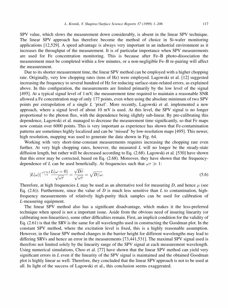
SPV value, which slows the measurement down considerably, is absent in the linear SPV technique.The linear SPV approach has therefore become the method of choice in Si-wafer monitoringapplications [12,529]. A speed advantage is always very important in an industrial environment as itincreases the throughput of the measurement. It is of particular importance when SPV measurementsare used for Fe concentration monitoring. This is because after Fe±B photo-dissociation themeasurement must be completed within a few minutes, or a non-negligible Fe±B re-pairing will affectthe measurement.
Due to its shorter measurement time, the linear SPV method can be employed with a higher choppingrate. Originally, very low chopping rates (tens of Hz) were employed. Lagowski et al. [12] suggestedincreasing the frequency to several hundred of Hz for reducing surface-state-related errors, as explainedabove. In this con®guration, the measurements are limited primarily by the low level of the signal[495]. At a typical signal level of 1 mV, the measurement time required to maintain a reasonable SNRallowed a Fe concentration map of only 177 points, even when using the absolute minimum of two SPVpoints per extrapolation of a single L `pixel'. More recently, Lagowski et al. implemented a newapproach, where a signal level of about 10 mV is used. At this level, the SPV signal is no longerproportional to the photon ¯ux, with the dependence being slightly sub-linear. By pre-calibrating thisdependence, Lagowski et al. managed to decrease the measurement time signi®cantly, so that Fe mapsnow contain over 6000 points. This is very important as experience has shown that Fe-contaminationpatterns are sometimes highly localized and can be `missed' by low-resolution maps [495]. This newer,high resolution, mapping was used to generate the data shown in Fig. 64.
Working with very short-time-constant measurements requires increasing the chopping rate evenfurther. At very high chopping rates, however, the measured L will no longer be the steady-statediffusion length, but rather will be decreased according to Eq. (2.68). Lagowski et al. [530] have shownthat this error may be corrected, based on Eq. (2.68). Moreover, they have shown that the frequency-dependence of L can be used bene®cially. At frequencies such that !� � 1:
jL�!�j !!��1 L�! � 0�������!�p �
������D�p������!�p �
���������D=!
p: (5.6)
Therefore, at high frequencies L may be used as an alternative tool for measuring D, and hence � (seeEq. (2.6)). Furthermore, since the value of D is much less sensitive than L to contamination, high-frequency measurements of relatively high-purity thick samples can be used for calibration ofL-measuring equipment.
The linear SPV method also has a signi®cant disadvantage, which makes it the less-preferredtechnique when speed is not a important issue. Aside from the obvious need of insuring linearity (orcalibrating non-linearities), some other dif®culties remain. First, an implicit condition for the validity ofEq. (2.61) is that the SRV is the same for all wavelengths used in constructing the Goodman plot. In theconstant SPV method, where the excitation level is ®xed, this is a highly reasonable assumption.However, in the linear SPV method changes in the barrier height for different wavelengths may lead todiffering SRVs and hence an error in the measurements [73,441,531]. The maximal SPV signal used istherefore not limited solely by the linearity range of the SPV signal at each measurement wavelength.Using numerical simulations, Choo et al. [77] have shown that the linear SPV method can yield verysigni®cant errors in L even if the linearity of the SPV signal is maintained and the obtained Goodmanplot is highly linear as well. Therefore, they concluded that the linear SPV approach is not to be used atall. In light of the success of Lagowski et al., this conclusion seems exaggerated.
L. Kronik, Y. Shapira / Surface Science Reports 37 (1999) 1±206 117
A key to the large difference between theory and experiment in this case may be found in the work ofHowland and Fonash [532]. These authors have compared between the two SPV methods for the caseof a Schottky contact. They concluded that if very low signal levels are used, the two methods are incomplete agreement. However, the linear SPV method begins to have problems at an SPV which is aslow as 0.61% of kT=e (!). We therefore conclude that while the linear SPV method can indeed be used,its validity should be examined very closely, preferably by a comparison to the results of the constantSPV method. For the case of a Schottky contact, Howland and Fonash recommended using a newtechnique, which they dubbed `Method C': We have already noted that the linearity of the short-circuitcurrent dependence on the illumination intensity is much better than that of the open-circuit voltage. Itis therefore advisable to use �exp�eSPV=kT� ÿ 1�, which is a measure of the short-circuit current, ratherthan the SPV itself, in the Goodman plot. An extension of this idea to MIS-based measurements has notbeen attempted yet.
Successful L measurements rely not only on reliable SPV measurements, but also on reliable absorptiondata. Theoretically, one would wish to complement SPV measurements with absorption measurementson the same sample. However, this is frequently not possible, and in many cases not desirable either(e.g., for industrial monitoring). This is particularly true for Si, where the spectral dependence of theabsorption coef®cient is supposedly very well known. Nevertheless, many scientists have observed thatsigni®cantly different values of L are obtained when using different absorption data given in theliterature [448,527,533]. In addition, it is very important to properly account for other effects which arenot taken into account in literature absorption data, but may be present in samples under study. Theseinclude free carrier absorption in heavily-doped samples [527] or photon recycling effects [519].
A speci®c problem in Si is the difference in absorption between stressed and stress-relieved layers,causing a relatively large scatter of absorption spectrum data. Nartowitz and Goodman [534] havecompared between diffusion lengths gathered using different absorption data, including thatrecommended by the ASTM protocol. They discovered that an uncertainty of many tens of percentmay ensue, especially for short diffusion lengths. Accordingly, they constructed a set of `compromise'absorption data which, when used over a narrower wavelength region where different absorption dataare in better agreement, reduces the uncertainty in L. However, the reduced wavelength range usedincreases the weight of errors in the illumination intensity.
Hwang and Schroder [456] have compared the Goodman plots obtained for Czochralski-grownmono-crystalline Si and cast poly-crystalline Si, shown in Fig. 65. While the mono-crystalline Siexhibits a conventional linear dependence of the photon ¯ux on the absorption length, as in, e.g.,Fig. 63, the poly-Si sample exhibits two linear regions with distinctly different slopes. From SPVinformation alone, it is impossible to determine which of the two, if any, should be extrapolated toobtain the true L. Using additional spectral response and short-circuit measurements, Hwang andSchroder have concluded that extrapolation of the short 1=� region represents the true L, whereas theextrapolation of the long 1=� region gives unrealistically high values of L. They have thus concludedthat stress in the poly-Si affects the absorption coef®cient mostly at longer wavelengths (correspondingto long 1=�), which are closer to the bandgap energy. By extrapolating the short 1=� of the Goodmanplot, they have been able to extract the correct dependence of � on wavelength at longer wavelengths.
Interestingly, Chiang et al. [520] used a similar concept for extrapolating the `absorption tail' ofInP : Mn samples at long wavelengths some ten years earlier. They based their extrapolation on theknown absorption coef®cient of InP at short wavelengths, assuming that the Mn-doping does not affect� signi®cantly for suf®ciently high photon energies.
118 L. Kronik, Y. Shapira / Surface Science Reports 37 (1999) 1±206
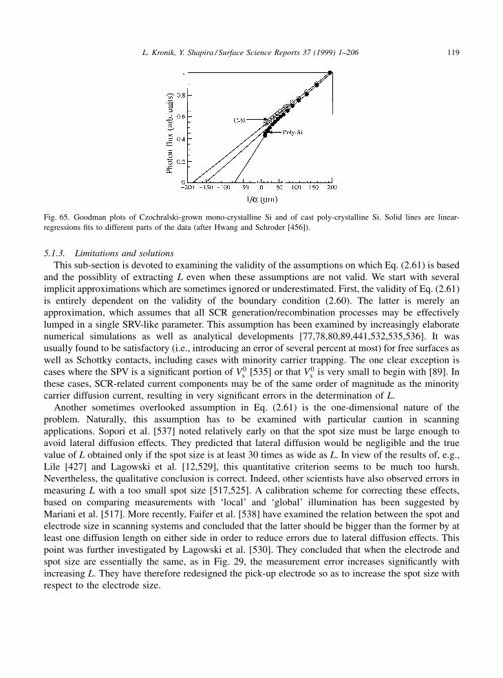
5.1.3. Limitations and solutions
This sub-section is devoted to examining the validity of the assumptions on which Eq. (2.61) is basedand the possiblity of extracting L even when these assumptions are not valid. We start with severalimplicit approximations which are sometimes ignored or underestimated. First, the validity of Eq. (2.61)is entirely dependent on the validity of the boundary condition (2.60). The latter is merely anapproximation, which assumes that all SCR generation/recombination processes may be effectivelylumped in a single SRV-like parameter. This assumption has been examined by increasingly elaboratenumerical simulations as well as analytical developments [77,78,80,89,441,532,535,536]. It wasusually found to be satisfactory (i.e., introducing an error of several percent at most) for free surfaces aswell as Schottky contacts, including cases with minority carrier trapping. The one clear exception iscases where the SPV is a signi®cant portion of V0
s [535] or that V0s is very small to begin with [89]. In
these cases, SCR-related current components may be of the same order of magnitude as the minoritycarrier diffusion current, resulting in very signi®cant errors in the determination of L.
Another sometimes overlooked assumption in Eq. (2.61) is the one-dimensional nature of theproblem. Naturally, this assumption has to be examined with particular caution in scanningapplications. Sopori et al. [537] noted relatively early on that the spot size must be large enough toavoid lateral diffusion effects. They predicted that lateral diffusion would be negligible and the truevalue of L obtained only if the spot size is at least 30 times as wide as L. In view of the results of, e.g.,Lile [427] and Lagowski et al. [12,529], this quantitative criterion seems to be much too harsh.Nevertheless, the qualitative conclusion is correct. Indeed, other scientists have also observed errors inmeasuring L with a too small spot size [517,525]. A calibration scheme for correcting these effects,based on comparing measurements with `local' and `global' illumination has been suggested byMariani et al. [517]. More recently, Faifer et al. [538] have examined the relation between the spot andelectrode size in scanning systems and concluded that the latter should be bigger than the former by atleast one diffusion length on either side in order to reduce errors due to lateral diffusion effects. Thispoint was further investigated by Lagowski et al. [530]. They concluded that when the electrode andspot size are essentially the same, as in Fig. 29, the measurement error increases signi®cantly withincreasing L. They have therefore redesigned the pick-up electrode so as to increase the spot size withrespect to the electrode size.
Fig. 65. Goodman plots of Czochralski-grown mono-crystalline Si and of cast poly-crystalline Si. Solid lines are linear-
regressions ®ts to different parts of the data (after Hwang and Schroder [456]).
L. Kronik, Y. Shapira / Surface Science Reports 37 (1999) 1±206 119

Another possible pitfall is that, as noted in Section 2.2.2, I in Eq. (2.61) is not the incident photon¯ux, but is rather the latter multiplied by the surface optical transmission and the sample quantumef®ciency. While most authors have found re¯ectivity variations to have a negligible effect on theresults in the narrow wavelength range usually probed, some have noted an in¯uence of re¯ectivity onthe results [446,469], especially for low values of L [527].
Eq. (2.61) also assumes a homogenous sample. Phillips [442] was the ®rst to theoretically investigatethe possible effects of an epitaxial layer with a different diffusion length on the apparent (extracted)diffusion length, Lapp. He has shown that the Goodman plot remains linear for any epitaxial layerthickness. However, Lapp re¯ects the true substrate diffusion length only if the epitaxial layer is thinnerthan half this diffusion length. Similarly, Lapp re¯ects the diffusion length of the epitaxial layer if thelatter is thicker than four times its diffusion length. For intermediate cases, Lapp is an effective valuewhich is not trivially related to any diffusion length.
The predictions of Phillips have been con®rmed experimentally by Gouskov et al. [451]. Theseauthors have extracted widely differing L values from electron beam induced current (EBIC)measurements, quantum ef®ciency curves, and SPV measurements (the latter in both contactless andshort-circuit current modes) at ITO/InP heterojunctions. These differences were attributed to a defectivesurface layer of �3 mm in the ITO/InP junction which has a much smaller diffusion length than the InPbulk. Damaged surface layers have also been observed to result in various non-linearities of theGoodman plot by Goodman et al. [486,534,539]. Speci®cally, Goodman has shown that a reducedquantum ef®ciency in a defective surface layer may distort the Goodman plot at short 1=� values [539].
More recently, Lowell et al. used wavelengths with low penetration depths for extracting the Fecontent in Si epitaxial layers using the SPV approach [540]. They showed that better correlation toDLTS and SIMS results is obtained with decreasing 1=� values. This is because more selective probingof the epitaxial layer is achieved. It should be noted that in their measurements the extracted L is stilllarger than the epitaxial layer thickness. Therefore, some contribution from the substrate cannot beavoided. Nevertheless, the weight of the epitaxial layer contribution is certainly enhanced, whichexplains the improved correlation with other techniques.
If the recombination centers which limit the diffusion length are inhomogeneously spread in thevertical direction, the resulting L would obviously be some average of the local L values. Someinformation about the vertical distribution of L may be obtained in a destructive manner by repeatedetch and measurement sequences [458,512]. Speci®cally, when used for Fe-monitoring purposes, itshould be remembered that the Fe contamination may vary as a function of sample depth, with the Femost detrimental to device performance found in the vicinity of the surface. This explains why the Fecontents measured by SPV and by techniques which only probe the SCR (e.g., those based oncapacitance transients) may differ [541,542]. The latter techniques are more directly relevant to deviceperformance. Nevertheless, SPV has been found to yield very good predictions to device performance,as discussed above.
While diffusion length measurements in non-homogenous samples should be treated with the utmostcaution, they are not necessarily erroneous. Contactless measurement of Si wafers has been shown to bepossible even when the wafer has an n� overlayer, is oxidized [12,491], or is even patterned withcircuits [12]. According to Phillips's theory, this is because the thickness of the overlayer(s) isnegligible with respect to the bulk diffusion length. It should be noted, however, that when measuringoxidized samples, special care should be taken to correct re¯ectivity changes due to interference, andalso a possible loss of signal due to oxide-passivation of the SCR [529]. Commercial SPV equipment
120 L. Kronik, Y. Shapira / Surface Science Reports 37 (1999) 1±206

has recently been installed with corona-induced oxide charging capabilities to overcome the latterobstacle.
Oxygen impurities are sometimes deliberately introduced into Si wafers, away from its surface, in orderto serve as internal gettering sources. This process yields a near-surface region, known as the denudedzone, which is relatively free of metallic impurities even if the wafer quality is not very high. Chappellet al. [543] suggested that such wafers may be modelled as a bulk region with low L and an epitaxiallayer with high L (i.e., opposite to the ITO/InP case studied by Gouskov et al. [451]). Using numericalsimulations, they concluded that if the denuded zone width is between the L values of the denuded zoneand the substrate, Lapp is proportional to the denuded zone width and may serve as an indicator of it.Although their analysis has later been shown to be too simplistic [531], it has been successfully used inpractice for at least qualitative determination of trends in denuded zone widths [487,544].
Except for the general underlying assumptions described above, Eq. (2.61) also relies on ®vequantitative limitations [5,531,545]. They are:
1=�� w; (5.7a)
L� w; (5.7b)
1=�� l; (5.7c)
L� l; (5.7d)
�n�w� � p or �p�w� � n; (5.7e)
where l is the sample thickness. All ®ve mathematical conditions have an immediate physical meaning.The ®rst two conditions state that the absorption depth, 1=�, and the diffusion length, L, must be muchlarger than the SCR width, w. This facilitates the neglect of SCR-related processes, mentioned above.The two following conditions state that both the absorption depth and diffusion length must be muchsmaller than the sample thickness. This means that neither photons nor excess carriers may reach theback sample surface, so that back-contact effects can be neglected. Finally, the ®fth condition impliesweak injection conditions. Unfortunately, in many cases the Goodman plots remain linear even if one ormore of the ®ve conditions is grossly violated [531]. However, in such cases Lapp may deviate from thetrue L very signi®cantly. This may be very misleading because the experimentalist cannot tell byinspection whether any of assumptions (5.7) have been violated or not. Therefore, a rigorousexamination of the validity of the ®ve conditions must be performed. Much theoretical andexperimental work has been devoted to extracting L even if some of the conditions (5.7) are notsatis®ed. The rest of this section is devoted to a detailed examination of such approaches.
In some cases, Goodman plots manifest a clear deviation from linearity in the short 1=� part of thecurve. Usually, the curves exhibit a minimum and a `curve up' part [464±466,523], as shown in Fig. 66[466]. This behavior is typical of a violation of condition (5.7a), 1=�� w. It is due to the ¯ow ofexcess carriers, formed in the SCR, towards the surface, in order to supply the surface recombinationcurrent [466]. This decreases the SPV and therefore a larger photon ¯ux is necessary to maintain thesame excess carrier density. The same effect is also responsible for the near-bandgap peak in SPS data(Fig. 41(a)), discussed in Section 4.1. If 1=�� w is valid at longer 1=�, than L can still be successfullyextracted, as long as the short 1=� region is not used in the extrapolation. Since this is almost alwaysthe case, little effort has been devoted to extracting L if 1=�� w is violated throughout the Goodmanplot.
L. Kronik, Y. Shapira / Surface Science Reports 37 (1999) 1±206 121
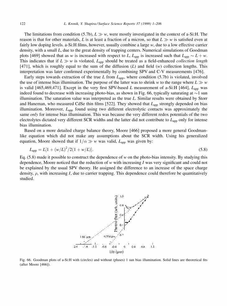
The limitations from condition (5.7b), L� w, were mostly investigated in the context of a-Si:H. Thereason is that for other materials, L is at least a fraction of a micron, so that L� w is satis®ed even atfairly low doping levels. a-Si:H ®lms, however, usually combine a large w, due to a low effective carrierdensity, with a small L, due to the great density of trapping centers. Numerical simulations of Goodmanplots [469] showed that as w is increased with respect to L, Lapp is increased such that Lapp � L� w.This indicates that if L� w is violated, Lapp should be treated as a ®eld-enhanced collection length
[471], which is roughly equal to the sum of the diffusion (L) and ®eld (w) collection lengths. Thisinterpretation was later con®rmed experimentally by combining SPV and C-V measurements [476].
Early steps towards extraction of the true L from Lapp, where condition (5.7b) is violated, involvedthe use of intense bias illumination. The purpose of the latter was to shrink w to the range where L� wis valid [465,469,471]. Except in the very ®rst SPV-based L measurement of a-Si:H [464], Lapp wasindeed found to decrease with increasing photo-bias, as shown in Fig. 66, typically saturating at �1 sunillumination. The saturation value was interpreted as the true L. Similar results were obtained by Storrand Haneman, who measured CdSe thin ®lms [522]. They showed that Lapp strongly depended on biasillumination. Moreover, Lapp found using two different electrolytic contacts was approximately thesame only for intense bias illumination. This was because the very different redox potentials of the twoelectrolytes dictated very different SCR widths and the latter did not contribute to Lapp only for intensebias illumination.
Based on a more detailed charge balance theory, Moore [466] proposed a more general Goodman-like equation which did not make any assumptions about the SCR width. Using his generalizedequation, Moore showed that if 1=�� w was valid, Lapp was given by:
Lapp � L�1� �w=L�2=2�1� w=L��: (5.8)
Eq. (5.8) made it possible to construct the dependence of w on the photo-bias intensity. By studying thisdependence, Moore noticed that the reduction of w with increasing I was very signi®cant and could notbe explained by the usual SPV theory. He assigned the difference to an increase of the space chargedensity, �, with increasing I, due to carrier trapping. This dependence could therefore be quantitativelystudied.
Fig. 66. Goodman plots of a-Si:H with (circles) and without (pluses) 1 sun bias illumination. Solid lines are theoretical ®ts
(after Moore [466]).
122 L. Kronik, Y. Shapira / Surface Science Reports 37 (1999) 1±206
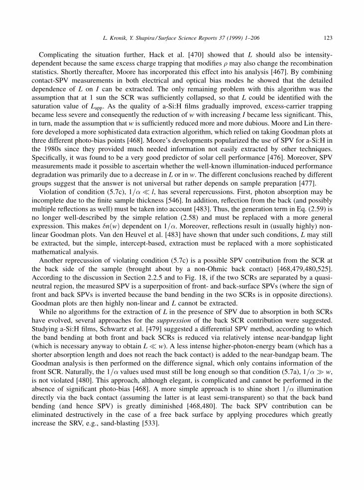
Complicating the situation further, Hack et al. [470] showed that L should also be intensity-dependent because the same excess charge trapping that modi®es � may also change the recombinationstatistics. Shortly thereafter, Moore has incorporated this effect into his analysis [467]. By combiningcontact-SPV measurements in both electrical and optical bias modes he showed that the detaileddependence of L on I can be extracted. The only remaining problem with this algorithm was theassumption that at 1 sun the SCR was suf®ciently collapsed, so that L could be identi®ed with thesaturation value of Lapp. As the quality of a-Si:H ®lms gradually improved, excess-carrier trappingbecame less severe and consequently the reduction of w with increasing I became less signi®cant. This,in turn, made the assumption that w is suf®ciently reduced more and more dubious. Moore and Lin there-fore developed a more sophisticated data extraction algorithm, which relied on taking Goodman plots atthree different photo-bias points [468]. Moore's developments popularized the use of SPV for a-Si:H inthe 1980s since they provided much needed information not easily extracted by other techniques.Speci®cally, it was found to be a very good predictor of solar cell performance [476]. Moreover, SPVmeasurements made it possible to ascertain whether the well-known illumination-induced performancedegradation was primarily due to a decrease in L or in w. The different conclusions reached by differentgroups suggest that the answer is not universal but rather depends on sample preparation [477].
Violation of condition (5.7c), 1=�� l, has several repercussions. First, photon absorption may beincomplete due to the ®nite sample thickness [546]. In addition, re¯ection from the back (and possiblymultiple re¯ections as well) must be taken into account [483]. Thus, the generation term in Eq. (2.59) isno longer well-described by the simple relation (2.58) and must be replaced with a more generalexpression. This makes �n�w� dependent on 1=�. Moreover, re¯ections result in (usually highly) non-linear Goodman plots. Van den Heuvel et al. [483] have shown that under such conditions, L may stillbe extracted, but the simple, intercept-based, extraction must be replaced with a more sophisticatedmathematical analysis.
Another reprecussion of violating condition (5.7c) is a possible SPV contribution from the SCR atthe back side of the sample (brought about by a non-Ohmic back contact) [468,479,480,525].According to the discussion in Section 2.2.5 and to Fig. 18, if the two SCRs are separated by a quasi-neutral region, the measured SPV is a superposition of front- and back-surface SPVs (where the sign offront and back SPVs is inverted because the band bending in the two SCRs is in opposite directions).Goodman plots are then highly non-linear and L cannot be extracted.
While no algorithms for the extraction of L in the presence of SPV due to absorption in both SCRshave evolved, several approaches for the suppression of the back SCR contribution were suggested.Studying a-Si:H ®lms, Schwartz et al. [479] suggested a differential SPV method, according to whichthe band bending at both front and back SCRs is reduced via relatively intense near-bandgap light(which is necessary anyway to obtain L� w). A less intense higher-photon-energy beam (which has ashorter absorption length and does not reach the back contact) is added to the near-bandgap beam. TheGoodman analysis is then performed on the difference signal, which only contains information of thefront SCR. Naturally, the 1=� values used must still be long enough so that condition (5.7a), 1=�� w,is not violated [480]. This approach, although elegant, is complicated and cannot be performed in theabsence of signi®cant photo-bias [468]. A more simple approach is to shine short 1=� illuminationdirectly via the back contact (assuming the latter is at least semi-transparent) so that the back bandbending (and hence SPV) is greatly diminished [468,480]. The back SPV contribution can beeliminated destructively in the case of a free back surface by applying procedures which greatlyincrease the SRV, e.g., sand-blasting [533].
L. Kronik, Y. Shapira / Surface Science Reports 37 (1999) 1±206 123

Violation of condition (5.7d), L� l, implies that carriers which are photo-excited in the vicinity ofthe front surface may reach the back one. It is therefore clear that even if there is no direct excitation ofthe back part of the sample (i.e., condition (5.7c), 1=�� l, is maintained), the sample cannot be treatedas semi-in®nite and the effects of the back surface must be taken into account. While Goodman plotsmade when condition (5.7c) is not valid frequently remain highly linear, it is clear that use of the simpleequations (2.61) or (5.3) should yield an erroneous value of L. Indeed, comparisons between SPV andPCD [445,547], mPCD [429,430], or electrolytic metal tracing (ELYMAT) [430,548] measurements onSi indicated a very good agreement for large sample thicknesses and a poor one for sample thicknessesapproaching the diffusion length. In recent years, this has become a more and more pressing problem,especially in industrially-oriented monitoring of Si wafers, due to the improvement in Si wafer quality.In the 1960s, diffusion lengths in Si wafers were of the order of tens of microns and the condition L� l
was easily satis®ed. In the 1990s, high-purity Si wafers typically feature diffusion lengths of at leastmany hundreds of microns and in some cases over a mm [529,549]. These values are of the order of, orexceed, typical wafer thicknesses. Thus, ironically, where the SPV method for Fe detection is supposedto be at its best because the diffusion lengths are very long, determining the Fe concentration using thesimple analyses described above becomes erroneous [498].
The effect of the back contact on the measured SPV, where the former is not directly illuminated,depends on whether the back contact and the back surface are one and the same. If this is indeed thecase (as in, e.g., the non-scanning SPV of ®lms deposited on a metallic substrate), some of the photo-excited carriers generated outside the back SCR will reach it nevertheless because the diffusion lengthis of the order of the sample thickness [550]. Thus, both SCRs would contribute to the measured SPV.Just as in the case of violating condition (5.7c), this means that L cannot be extracted, unless Sb is veryhigh and the back-SCR-related SPV is negligible.
In many cases, the back-contact is not the same as the back surface. For example, in scanningapplications the back-contact (which can also be capacitive) may be placed on a small portion of thesample. If this contact is suf®ciently well-removed from the illumination spot, photo-excited carrierscannot reach its vicinity even by diffusion. In such cases, the back surface affects the front SPV bymodifying the excess carrier density, but does not contribute directly to the measured SPV. Back-surface effects are usually expressed quantitatively by replacing the semi-in®nite sample boundaryconditions with a SRV-type condition:
Dd�n�x�
dx
����x�l
� ÿSb�n�l�; (5.9)
where Sb is the back-surface SRV, and solving the continuity equation (2.59).Anttila and Hahn [531] examined the relation between Lapp, extracted from a simple Goodman plot,
and the real L, by performing extensive simulations, based on including the back surface boundarycondition (5.9). A typical result is shown in Fig. 67 [531]. As long as L � l, Lapp � L. For larger L=lratios, Lapp is highly dependent on Sb. For high (low) values of Sb, L is highly underestimated(overestimated) by Lapp. Unrealistically large and small apparent diffusion lengths correlated with lowand high Sb, respectively, have indeed been observed by several groups [429,513,547,548]. Thedemarcation line between the two phenomena lies at Sb � D=L, for which Lapp � L, regardless ofsample thickness. These results may be readily explained in physical terms: Sb � D=L implies that theback SRV is equal to the diffusion velocity. In this case, the recombination current at x � l is equal tothe diffusion current which would have existed at x � l had there not been a back contact there.
124 L. Kronik, Y. Shapira / Surface Science Reports 37 (1999) 1±206
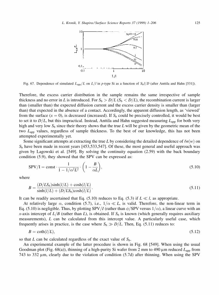
Therefore, the excess carrier distribution in the sample remains the same irrespective of samplethickness and no error in L is introduced. For Sb > D=L (Sb < D=L), the recombination current is largerthan (smaller than) the expected diffusion current and the excess carrier density is smaller than (largerthan) that expected in the absence of a contact. Accordingly, the apparent diffusion length, as `viewed'from the surface (x � 0), is decreased (increased). If Sb could be precisely controlled, it would be bestto set it to D=L, but this impractical. Instead, Anttila and Hahn suggested measuring Lapp for both veryhigh and very low Sb since their theory shows that the true L will be given by the geometric mean of thetwo Lapp values, regardless of sample thickness. To the best of our knowledge, this has not beenattempted experimentally yet.
Some signi®cant attempts at extracting the true L by considering the detailed dependence of �n�w� onSb have been made in recent years [453,533,547]. Of these, the most general and useful approach wasgiven by Lagowski et al. [549]. By solving the continuity equation (2.59) with the back boundarycondition (5.9), they showed that the SPV can be expressed as:
SPV=I � const � 1
1ÿ 1=�2L2� 1ÿ B
�L
� �; (5.10)
where
B � �D=LSb�sinh�l=L� � cosh�l=L�sinh�l=L� � �D=LSb�cosh�l=L� : (5.11)
It can be readily ascertained that Eq. (5.10) reduces to Eq. (5.3) if L� l, as appropriate.At relatively large �, condition (5.7), i.e., 1=�� L, is valid. Therefore, the non-linear term in
Eq. (5.10) is negligible. Thus, by plotting SPV=I (rather than �=SPV versus 1=�), a linear curve with anx-axis intercept of L=B (rather than L), is obtained. If Sb is known (which generally requires auxiliarymeasurements), L can be calculated from this intercept value. A particularly useful case, whichfrequently arises in practice, is the case where Sb � D=L. Then, Eq. (5.11) reduces to:
B � coth�l=L�; (5.12)
so that L can be calculated regardless of the exact value of Sb.An experimental example of the latter procedure is shown in Fig. 68 [549]. When using the usual
Goodman plot (Fig. 68(a)), thinning of a high-purity Si wafer from 2 mm to 490 mm reduced Lapp from743 to 332 mm, clearly due to the violation of condition (5.7d) after thinning. When using the SPV
Fig. 67. Dependence of simulated Lapp=L on L=l in p-type Si as a function of Sbl=D (after Anttila and Hahn [531]).
L. Kronik, Y. Shapira / Surface Science Reports 37 (1999) 1±206 125
versus 1=� plot (Fig. 68(b)), the initial part of the curve, where 1=�� L, was indeed linear. Using theintercept values of the plot with Eq. (5.12), L values of 749 and 760 mm were obtained before and afterthinning, respectively. These values are in excellent agreement with the L obtained from the Goodmanplot prior to thinning. A further check on the correctness of the result is that after correcting themeasured data for the non-linear term in Eq. (5.10), based on the now-known value of L, an excellent ®twith the extrapolation of the straight line is obtained.
We note in passing that a calibration chart for obtaining the true L from Lapp based on wafer thicknessand assuming an in®nite Sb is now included in the ASTM standard [424]. In light of the abovediscussion, it is clear that the calibration should be different if Sb is ®nite.
The ®fth and ®nal condition (5.7e), states that for measuring the minority carrier diffusion length theinjection level must be low. As explained in Section 2.2.4, if the injection level is not low enough, theelectric ®eld across the quasi-neutral region, i.e., the Dember ®eld, is not necessarily negligible. Then,the ambipolar transport equation (2.93) must be used instead of the more simple equation (2.59). Thus,the assignment of an experimentally obtained diffusion length to the minority carrier diffusion length isequivalent to assuming that the illumination intensity was low enough to ensure a negligible Dembereffect. The qualitative considerations given here have been fully con®rmed by numerical simulations.Early numerical simulations by Choo and Anderson [441] showed that at low illumination intensities,SPV measurements can be applied successfully even to samples with minority carrier trapping centers.This is because the Dember ®eld is usually negligible even in the presence of minority carrier trapping,unless the latter is very signi®cant. More recent numerical simulations performed by Zhang et al. [536]showed that at high illumination intensities, the apparent L departs from its real value (in a manner thatis SRV-dependent).
The fact that SPV can (and should) be used under low-injection conditions is a signi®cant advantageof the technique with respect to other methods which rely on high-level excitation, such as mPCD orELYMAT [428,430,551]. In the latter techniques, the obtained lifetime cannot be directly related to theminority carriers without further information. Similarly, a possible in¯uence of excess charge carrierson the `true' minority carrier diffusion length must be taken into account when performing SPV
Fig. 68. (a) Normal `linear SPV' Goodman plot of a high purity 2 mm thick Si wafer, before and after thinning to 490 mm. (b)
SPV vs. 1=� plot of the same sample. Open and ®lled symbols correspond to the as-measured values and the values corrected
for the non-linear term in Eq. (5.10), respectively. All curves were measured using a constant photon ¯ux (after Lagowski et al.
[549]).
126 L. Kronik, Y. Shapira / Surface Science Reports 37 (1999) 1±206
measurements with a photo-bias or with an increased illumination intensity. For example, the apparentL in ribbon Si solar cells has been shown (using SPV [450] as well as other techniques [552]) toincrease with increasing illumination intensity due to trap ®lling.
If the injection level is fairly high, i.e., the Dember effect contribution is very signi®cant, theambipolar mobility �a tends to zero (see Eq. (2.94)). This means that the electric ®eld term in theambipolar transport equation (2.93) may be neglected. This equation than reduces to the form ofEq. (2.59), except that the coef®cients D, � , and L are the ambipolar coef®cients, rather than theminority carrier ones. This may be used bene®cially for extracting the ambipolar diffusion length insamples where the doping level is very low and the Dember effect is expected to be signi®cant. Forexample, Liu et al. [118] showed (both theoretically and experimentally) that in semi-insulating GaAssamples, the SCR-related SPV is negligible with respect to the Dember-related SPV. Due to thesimilarity between Eqs. (2.93) and (2.59), the Dember-related SPV obeys an equation which is just likeEq. (5.3), except that Ln is replaced by La. Therefore, it is the latter which is extrapolated from anappropriate plot.
The most controversial aspect of condition (5.7e) has to do with undoped a-Si:H ®lms. These ®lmstypically exhibit very low equilibrium carrier concentrations. Therefore, it has been argued, startingfrom the earliest papers dealing with SPV measurements of such ®lms, that the extrapolated L is equalto La [464±466]. Some doubt has been cast on this `standard' conclusion by McElheny et al. [553].Using detailed numerical simulations, they showed that in the presence of signi®cant trapping (which isubiquitous in a-Si:H), the SPV is due to various drift and diffusion current components which dependon the excitation level in a non-trivial manner. In some cases, the calculated current components werenot even in the same direction. Moreover, these authors claimed that the obtained L cannot even be usedas a qualitative criterion for cell performance because in some of the simulations samples whichyielded a smaller Lapp were calculated to exhibit a better, rather than worse, solar cell performance.McElheny et al. suggested that the SPV method can be trusted only if trapping is greatly reduced, e.g.,in samples with deliberate n-type doping and trap densities below 1013 cmÿ3.
Shortly thereafter, Hegedus et al. [477] pointed out that no physical reason accounting for thedifferent direction of drift and diffusion currents was provided by McElheny et al. They also pointedout that the signi®cant empirical success of SPV measurements in predicting the performance ofa-Si:H-based solar cells was dif®cult to reconcile with the pessimistic ®ndings of McElheny et al.Hegedus et al. therefore called for a comparison between the results of SPV and those of a differentL-measuring technique, which had emerged at that time ± the steady-state photocarrier grating (SSPG)approach [554]. This is because of the immunity of SSPG to electric ®eld effects. This call wasanswered by Balberg et al. [481]. They concluded that SPV measurements do not yield the true La, butrather a quantity which depends on it in a non-trivial manner. This is probably because even at thehighest photo-bias intensities used by Balberg et al. a complete collapse of the SCR was not obtained.Nevertheless, these authors concluded that the predictive power of SPV is much better than thatexpected from the numerical simulations of McElheny et al. On the other hand, van den Heuvel et al.[484] maintained that the drift currents found by McElheny et al. are simply a manifestation of theDember ®eld and that the SPV method does yield La and can be used safely. In our opinion, the issuehas not been fully settled. Unfortunately, it has not been studied further. This is because the doubts caston the SPV technique on the one hand, and the success of SSPG in circumventing similar dif®culties onthe other hand, caused the a-Si:H community to almost invariably prefer the latter approach. Thus, theapplication of SPV to a-Si:H was practically abandoned in the 1990s.
L. Kronik, Y. Shapira / Surface Science Reports 37 (1999) 1±206 127
In conclusion, we note that diffusion length measurements are a highly evolved, useful, andsuccessful area of the SPV technique. If due attention is paid to limiting conditions and properinterpretation, results of both scienti®c and technological importance are obtained.
5.2. Surface band bending and dipole
Detailed information on the electronic band structure at semiconductor surfaces, expressed in theform of a schematic band diagram (see Fig. 4), plays a central role in many studies of surface chemicalreactions, e.g., studies of adsorption/desorption and oxidation/reduction processes. Similar informationis extremely important for studies on the formation of semiconductor interfaces, where, typically, theproperties of a substrate with a very thin (metallic or semiconducting) overlayer are studied[23,24,555].
If the bulk band-diagram is known, information on the equilibrium surface band-bending, V0s , and the
surface dipole, ��s, makes possible the construction of the surface band-diagram, shown in Fig. 4. Wenote that (if the bulk doping is known) knowledge of V0
s is equivalent to knowledge of the equilibriumsurface charge, Qss. This is a result of the charge neutrality condition, Qss � ÿQsc, and the one-to-onecorrespondence between Qsc and V0
s , expressed in Eq. (2.30). The SPV-based extraction of the surfaceband-bending/charge and of the surface dipole are discussed in detail in this section.
5.2.1. Surface band bending ± photosaturation
The most used SPV-based tool for determining V0s is the photosaturation technique. This method,
which is very simple in nature, is based on assuming that application of suf®ciently intense super-bandgap illumination to the semiconductor surface results in complete ¯attening of the surface bandbending. The basis for this assumption lies with Eq. (2.52), which describes Qsc under illumination as afunction of the injection ratio, �n. This equation predicts that for �n !1, Qsc ! 0, and henceVs ! 0, regardless of V0
s . Thus, V0s is obtained experimentally as equal and opposite to the SPV
measured under intense illumination.Williams seems to have been the ®rst to utilize the photosaturation technique (as early as 1962), in
the course of studying oxygen adsorption and desorption on CdS surfaces [556]. Since thephotosaturation approach is relatively easy to implement and very simple to interpret, many otherstudies have utilized it for determining V0
s values at various semiconductor surfaces. These studiesinclude further investigations of oxygen adsorption/desorption at CdS surfaces [557]; CdS/insulatorinterfaces [558]; a-Se/organic polymer interfaces [559]; Ambient effects on GaAs(111) surfaces [560±562]; Effects of different etching reagents on (100) InP surfaces [563]; Effect of organic moleculeadsorption on various semiconductors [50±57]; Temperature-dependence of the surface potential in Si[564,565], Ge [567,568], GaAs [569] and SiC [570]; Laser-induced modi®cation of the Si/SiO2
interface [565]; Band-diagrams of Cd-based II±VI semiconductors [571]; Band-diagrams of variousclean [11,289] and real [572±574] Si surfaces; Band-diagrams of a-Si:H surfaces [303,575±577]; Band-diagrams of organic semiconductors [412±414]; and band-diagrams of Ge [573], CdTe [384], CdMnTe[393], and NiO [578] surfaces. In addition, Brillson et al. have used the photosaturation techniqueextensively for characterizing the in¯uence of metallic overlayers on the band bending at CdS[372,373,579,580], GaAs [579,581,582], and ZnO [583] surfaces.
In the early 1990s, Edelman et al. introduced wafer scale mapping of the surface charge at Si wafers,which is based on scanning the saturation SPV using the machine shown in Fig. 29 [584±586]. This
128 L. Kronik, Y. Shapira / Surface Science Reports 37 (1999) 1±206

produces surface charge maps, which can complement the diffusion length and Fe concentration mapsshown in Fig. 64. Surface charge mapping has been successfully adopted, extended, and applied tomonitoring of a wide variety of wafer processing steps by Nauka et al. [506,587±591] and Lowell et al.[507±509,592±601]. The SPV-measured charge at dielectric covered Si wafers has been shown to be invery good agreement with the charge deduced from C±V measurements [587]. This agreement wasobtained even though the two results do not have to agree completely because of the additionalprocessing steps needed for the C±V measurements. However, the contactless, non-destructive nature ofthe SPV-based approach makes it much more suitable for in-line monitoring and process control. Naukahas also extended the approach to mapping of the charge at the buried Si/dielectric interface of silicon-on-insulator wafers [589].
Photosaturation has also been used for performing a V0s -determining step in SPV-based algorithms
for extracting surface state energy distributions [565,568,569,572,602,603] and surface-state properties[110,319,604], which are described in Section 5.4. Similarly, it has been used as a step in an algorithmfor constructing the band diagram of semiconductor heterojunctions, discussed in Section 5.5.3[19,403,605]. It was also used for calibration of barrier heights in ®eld-effect measurements [562,606].
Despite the host of applications described above, many of which have been very successful, oneshould bear in mind that photosaturation is one of the most controversial and pitfall-laden quantitativeSPV-based approaches. Therefore, much room is devoted in this section to a detailed discussion of itslimitations and the conditions for its validity.
It is usually agreed that in order to ascertain experimentally that band ¯attening has been achieved,the SPV must be measured as a function of incident illumination intensity. A saturation of the resultingSPV � f �I� curve at the highest illumination intensities is taken as evidence of ¯at bands (hence the namephotosaturation). The source of the controversy is that examinations of the SPV � f �I� curves haveproduced mixed results: In some studies photosaturation was consistently obtained (see, e.g., [303,384,557,563,572,573,576,602]), whereas in others it was consistently not obtained (see, e.g., [214,607±610]).
In yet a third group of studies, photosaturation was obtained for some, but not all, surface conditions[412,556,558,561,575]. This third kind is the most interesting, as it provides a key for understanding theeffects which govern the elusive photosaturation behavior. An example is given in Fig. 69, which showsthe photosaturation measurements of Flinn and Briggs on n- and p-type GaAs(1 1 1) samples, exposedto different gases [561]. It is readily observed that the SPV does not saturate for any of the p-typesamples or for the nitrogen exposed n-type samples. Saturation is obtained for the n-type oxygen-exposed sample and perhaps also for the oxygen and ozone exposed n-type sample, although in thelatter case the saturation is somewhat less pronounced and is not necessarily complete.
The general validity of the photosaturation technique, as well as the conditions under which it isexpected to succeed experimentally, have been recently examined theoretically by Aphek et al. [611].They used a simple analytical model, based on the quasi-Fermi level approximation and on the`Goodman' (Moss) equation (see Section 2.2.2), as well as a rigorous numerical solution, to constructsteady-state SPV� f �I� curves. The results of these calculations are shown in Fig. 70. A constant kn
was used in the calculations because kn was found to govern the SRV in this case. Since the SRV wasmaintained at a constant value, the �p�w�=I ratio was approximately equal in all curves (see Eq. (2.61)),which facilitated a comparison of different curves on the same SPV� f �I� plot. Furthermore, for a®xed �p�w�=I ratio, the variation between the different curves was found to depend on kp=kn, ratherthan their individual values. Fig. 70 allows much useful insight into photosaturation mechanisms and isused as a basis for our discussion.
L. Kronik, Y. Shapira / Surface Science Reports 37 (1999) 1±206 129

An interesting and general observation is that all curves shown in Fig. 70 are bound between twoenvelope (i.e., limiting) curves on the left and right, corresponding to very small and very large valuesof kp, respectively. Several asymptotic SPV regimes are common to all curves shown in the ®gure: Forvery low injection, the SPV is very small (i.e., less than kT=e). We refer to this regime as the `nullregime'. At some critical point, which is in the low-injection regime, but the value of which is differentfor the different curves, the (absolute value of the) SPV starts to rise in an approximately logarithmicmanner. We refer to this regime as the `logarithmic regime'. For large enough illumination intensities,the SPVof the low kp curves saturates at a value which is indeed equal and opposite to V0
s over a certaininterval of I values (the `saturation regime'). For all curves, the (absolute value of the) SPV diminishesat very high intensities (the `Dember interference regime').
The behavior of all different curves in Fig. 70 may be explained physically. Photo-excited excesscarriers have been suggested to induce ¯attening of the surface band-bending via two distinctmechanisms: The ®rst mechanism is screening of the surface charge by free carriers [22,66]. Namely,the photo-injection of majority carriers allows for a compensation of the surface state charge over anarrower SCR, i.e., the necessary Qsc is accumulated over a smaller SCR width. The narrower the SCR,
Fig. 69. SPV � f�I� curves at GaAs(111) surfaces in various ambients. Full circles: nitrogen; empty circles: oxygen; crosses:
oxygen and ozone (after Flinn and Briggs [561]).
Fig. 70. Calculated steady state SPV � f�I� curves for a 5�1016 cmÿ3 p-type GaAs sample, having a surface state located 0.87
eV above the valence band edge, with a density of 5�1011 states/cm2, kn � 10ÿ19 cm2, and various kp values (in cm2).
(a) Numerical calculations. (b) Analytical calculations (after Aphek et al. [611]).
130 L. Kronik, Y. Shapira / Surface Science Reports 37 (1999) 1±206
the smaller the band-bending is. Finally, under suf®ciently intense illumination, the SCR width isexpected to be negligible and the bands should become ¯at. The second mechanism is directmodi®cation of the surface charge through carrier trapping [556,582]. The extent of this process isstrongly dependent on the ratio of the surface state hole and electron capture coef®cients, kp=kn. If thelatter is large, the surface state captures holes more effectively than electrons and its charge tends tobecome more positive upon illumination. Similarly, if kp=kn is small, the surface charge tends tobecome more negative upon illumination.
The dependence of the second mechanism on kp=kn is the cause for the `family of curves' in Fig. 70.For large kp, the surface charge increases upon illumination, so band ¯attening may proceed only viascreening, which necessarily requires high injection [611]. The smaller kp is, the more effectively canthe surface donor state capture electrons and hence diminish the surface charge. Thus, band-¯attening isassisted (and at low enough kp=kn ratios dominated) by direct surface charge modi®cation, which makesphotosaturation obtainable at fairly low injection levels.
Not all curves in Fig. 70 saturate at the correct value for suf®ciently high illumination intensity, dueto the Dember effect [79,611]. As easily veri®ed using Eq. (2.92), under high injection conditions,where the excess carrier density approaches the equilibrium majority carrier density, the Dembercontribution to the measured SPV is non-negligible. The Dember contribution to the SPV is alwayspositive (see Section 2.2.4). When it interferes with p-type SPV � f �I� curves, a pseudo-saturation, at avalue that is different from ÿV0
s , should be observed over some intensity range. In the case of n-typesamples, the Dember contribution should mask the photosaturation because the Dember voltagecontinues to increase even after the SCR-related SPV saturates.
Based on Fig. 70, the following picture emerges: In principle, suf®ciently intense illumination does
¯atten the surface band bending, so that the theoretical concept behind the photosaturation approach isvalid. However, important basic limitations arise, which preclude the attainment of V0
s fromSPV � f �I� curves in many practical cases. We now turn to analyzing the limitations of thephotosaturation technique and the results of past photosaturation experiments, based on the foregoingdiscussion.
One problem associated with high-intensity illumination is that in many cases sample heating and/orsurface photochemical processes may hinder the attainment of photosaturation, due to irreversibleillumination-induced changes in the sample physical properties. Bruening et al. have estimated the errorintroduced by such changes by measuring SPV � f �I� curves using both increasing and decreasingillumination intensity, and estimating the ensuing hysteresis [52]. This may limit the maximalillumination intensity which may be used. A practical limitation to the maximal intensity is imposed bythe light sources available. As shown in Fig. 70, the illumination intensity required for the attainment ofphotosaturation varies over many orders of magnitude, depending on the surface state properties. Thelatter are seldom well-known a priori. Therefore, the attainment of photosaturation cannot beguaranteed a priori and the experiment may fail.
Many of the total or partial failures of the photosaturation technique can be understood on the basisof an inadequate illumination intensity coupled with an unfavorable kp=kn value. For example,analytical calculations similar to those behind Fig. 70 were performed in [610]. These calculations,which were restricted to a limited range of illumination intensities and cross-section ratios, predicted atotal failure of the photosaturation technique. Let us consider the experiments of Flinn and Briggs,shown in Fig. 69, as another illustrative example. An upper limit for �p=I in their experiment may befound from Eq. (2.61), assuming S � 0, �L�1� �L� ! 1, and using typical values for carrier mobility
L. Kronik, Y. Shapira / Surface Science Reports 37 (1999) 1±206 131
and lifetime in GaAs. Given the maximal illumination intensity used in their experiment (1018
cmÿ2 secÿ1), it turns out that the excess carrier density in the experiment was at least two orders ofmagnitude below the doping level (which was 3�1015 cmÿ3). It is therefore evident that strong injectionwas not obtained by Flinn and Briggs. Thus, band ¯attening by screening, as well as Dember-relatedeffects, can be ruled out in the Flinn and Briggs experiment. Hence, it is clear that in those curves ofFig. 69 where saturation was observed, direct surface-charge modi®cation, enabled via a favorablekp=kn ratio, was the saturating mechanism.
More information on the saturation mechanism at work can be obtained from considering thelogarithmic regime, where the SPV is approximately given by [612]:
jSPVj � ��kT=e�ln �BI�; (5.13)
where � and B are proportionality factors. Interestingly, a relation of the form of Eq. (5.13) is predictedfor some illumination regime by all theoretical approaches, including calculations based on thedepletion approximation [556], on barrier SPV [557], on a Schottky-diode approach [193,214], on theconstant quasi Fermi level approximation [610,611], and even on the Dember effect [79,116]. Apheket al. [611] have found that if kp=kn is either very large or very small, � will be approximately 1 (and inpractice somewhat smaller [214]), whereas for intermediate values of kp=kn, � is approximately 0.5.These ®ndings are in agreement with the physical prediction of Bednyi and Baidus [612], whointerpreted � as being equivalent to the ideality factor in a Schottky diode. Accordingly, � should beideal (i.e., 1) for a pure barrier SPV, and smaller than 1 when surface trapping of excess carriers ispresent. Similarly, � � 2 in the presence of signi®cant bulk trapping, just like in a Schottky diode[366,612].
Since � is the slope of the SPV � f �I� curve on a semi-logarithmic plot, its value can be easilydeduced from a given experiment and used to assess the dominating photosaturation mechanism. Forexample, the slopes of all SPV � f �I� curves in Fig. 69 related to n-type samples are within �10% of 1.Since saturation is obtained for the oxygen-exposed sample and since screening is ruled out, weconclude that this curve, and probably the other two as well, are left (large kp=kn) envelope curves. Asnoted above, the curve of the oxygen and ozone exposed sample also seems to saturate, but thissomewhat less pronounced saturation is not necessarily true. It may also be due to a cross-over from thelarge kp=kn to the intermediate kp=kn regime (compare with the kp � 10ÿ23 cm2 curve in Fig. 70). Suchtransitions provide another source for photosaturation misinterpretations. The curve slopes of the p-typesamples in Fig. 69 are all within �20% of ÿ0:5. Therefore, they are probably intermediate kp=kn
curves. Since saturation is harder to obtain at intermediate kp=kn curves than at left envelope curves, itis no surprise that saturation was not obtained at the p-type samples. Moreover, the illuminationintensity at the rise point of the p-type curves is approximately four orders of magnitude larger than thatat the rise points of the n-type curves. This is consistent with the predictions of Fig. 70, although thedifference may also be due to a different injection ratio.
It is important to distinguish between direct- and indirect-gap materials in photosaturation attempts.The diffusion length in the former is usually considerably smaller than in the latter. Hence, usingEq. (2.61), we conclude that �p=I in direct-bandgap materials is such that large injection ratios are verydif®cult to obtain. In indirect-bandgap materials large injection ratios are easier to obtain, as long as S isnot too large. Indeed, many photosaturation measurements of Si or Ge samples feature completesaturation [572,573,602], or at least a departure from the logarithmic regime at the highest intensities,which may indicate an approach to saturation [11].
132 L. Kronik, Y. Shapira / Surface Science Reports 37 (1999) 1±206
Photosaturation is expected to be easier to obtain the smaller V0s is. However, at very low band-
bending, the SPV due to selective trapping of carriers at the surface may become dominant, in whichcase the SPV does not necessarily re¯ect V0
s even in sign (see Section 4.1). Kumar and Agarwal havecalculated the importance of this effect for a-Si:H samples. They concluded that because of signi®cantbulk trapping, Qsc was not altered signi®cantly and most of the SPV signal was due to selective carriertrapping at the surface, rather than due to a change in Qsc [613]. This was demonstrated by varioussurface treatments which produced SPV changes uncorrelated with conductivity changes. Theytherefore concluded that the photosaturation technique is not suitable for a-Si:H at all. However, asnoted above, Fig. 70 suggests that selective carrier trapping does not necessarily contradictphotosaturation and that indeed it is frequently the dominating photosaturation mechanism. Moreover,the extent of the change in Qsc is not necessarily negligible for any trap distribution envisaged or forany reasonable illumination intensity. Nevertheless, the work of Kumar and Agrawal does suggest thatphotosaturation measurements of amorphous semiconductors should be approached with even morecaution than usual.
As discussed in Section 2.2.2, the SPV increases with decreasing temperature because thermaltransitions, which compete with the optically-induced transitions, are suppressed. Thus, photosaturationshould be easier to obtain at lower temperatures. For example, MoÈnch has shown that the SPV � f �I�curve at the Si(111)-(7�7) surface, which is metallic in nature, does not saturate completely at roomtemperature, but features a very pronounced saturation at 85 K [11]. Similar trends have been observedat a-Si:H ®lms by Foller et al. [577].
Much of the controversy surrounding the photosaturation technique is due to the work of Brillsonet al., who studied the evolution of both CPD and SPV with metal overlayer thickness at differentsemiconductor surfaces [372,579±583]. Speci®cally, the results obtained at the Al/GaAs(1 1 0) interface[579,581,582], shown in Fig. 71 [582], were the source of a signi®cant debate between Spicer et al. andBrillson [614±616]. Brillson interpreted the SPV obtained at the maximal photon intensity in Fig. 71(a)as indicative of ÿV0
s . He therefore interpreted the increase of the SPV up to �6 AÊ as indicating thatthe band bending at the Al/GaAs(1 1 0) interface does not reach its maximum value at sub-monolayerAl coverages. This was in direct con¯ict with the results of Spicer et al., obtained using PES [617].In response, Spicer et al. [614] argued that, in the presence of a metallic overlayer, the SPV shouldbe analyzed in terms of an illuminated Schottky barrier, rather than in terms of a free surface. Theythen argued that this precludes the achievement of photosaturation at the maximal illuminationintensity used in Fig. 71(a). Moreover, Spicer et al. considered the lowest-intensity value in eachof the curves in Fig. 71(a) as being due to surface states and not due to the bulk effect. Subtractingthis value out produced a fairly constant SPV value, which Spicer et al. took as representing aconstant V0
s .A closer look at the photosaturation data of Fig. 71(a) and at the debate between Spicer et al. and
Brillson sheds some more light on photosaturation interpretations and misinterpretations: In Fig. 71(a),the low-coverage curves (e.g., the 0.7 AÊ overlayer curve) seem to approach saturation, which suggeststhat V0
s may be assessed. While this may indeed be the case, a different explanation should also beconsidered [611]. The most signi®cant difference between the analytical model and the numericalsimulations in Fig. 70 is that the numerically calculated kp � 10ÿ19 cm2 and kp � 10ÿ23 cm2 curvesdeviate rather strongly from the analytical ones. In the logarithmic regime, they feature an additional`shoulder'. This is because in this region, the assumption of constant quasi-Fermi levels is not quiteadequate. The `shoulder' at the 0.7 AÊ in Fig. 71(a) is very reminiscent of the curve corresponding to
L. Kronik, Y. Shapira / Surface Science Reports 37 (1999) 1±206 133
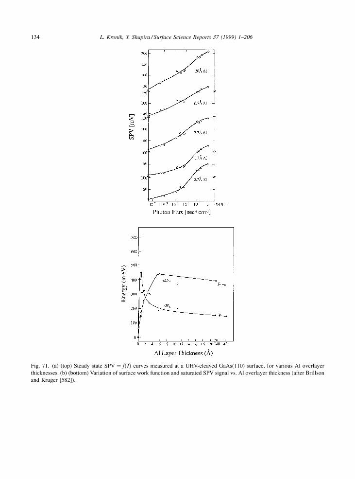
Fig. 71. (a) (top) Steady state SPV � f�I� curves measured at a UHV-cleaved GaAs(110) surface, for various Al overlayer
thicknesses. (b) (bottom) Variation of surface work function and saturated SPV signal vs. Al overlayer thickness (after Brillson
and Kruger [582]).
134 L. Kronik, Y. Shapira / Surface Science Reports 37 (1999) 1±206
kp � 10ÿ19 cm2 in Fig. 70(a). According to this explanation, the decreasing slope of the experimentalcurve at high intensities may be related to a return to the constant quasi-Fermi level approximationconditions, rather than to the attainment of `real' photosaturation.
The saturation in Fig. 71(a) is more and more marginal with increasing overlayer intensity, until it ispositively absent at the highest coverages (e.g., 20 AÊ ), where the SPV � f �I� curves do not deviatefrom the logarithmic regime even at the highest illumination intensities used. Accordingly, Brillson etal. have not considered the SPV values for thicknesses over �6 AÊ as representing true saturation[582,615]. The attainment of photosaturation is indeed expected to be particularly dif®cult in thepresence of a metallic overlayer. First, metal deposition typically increases the SRV and reduces the netphoton ¯ux entering the sample. Both effects decrease the �p=I ratio. Second, as the overlayerthickness increases, its properties are increasingly more `metallic'. Therefore, in the case of a thickenough metal overlayer it is indeed more appropriate to analyze the SPV in terms of an illuminatedSchottky junction, as suggested by Spicer et al. Nevertheless, an analysis in terms of surface staterepopulation was correctly suggested by Brillson for thin overlayers, where metallic behavior is notestablished. Since, as argued above, photosaturation is frequently dominated by surface staterepopulation, a subtraction of some of the surface state contribution, as performed by Spicer et al., isstrictly forbidden. Accordingly, it seems that much of the debate between Spicer et al. and Brillson canbe reduced to whether the overlayers can be considered as `metallic' or not. Unfortunately, the onset of`metallic behavior' is ill-de®ned and is frequently a subject of debate [618]. It can, however, be saidthat the thicker the overlayer is, the more dif®cult surface state repopulation (and hence the attainmentof photosaturation) becomes. This is well re¯ected in Fig. 71(a). Since we have already concluded thatphotosaturation via screening is virtually impossible in steady-state measurements of GaAs, theeffectiveness of the photosaturation technique for metal-covered GaAs surfaces is indeed very limited,and its use should be treated with the utmost caution.
As noted above, if strong injection can be obtained, saturation may be obscured by a `parasitic'contribution of the Dember potential. This was already noted in the early studies of Williams. Henoticed that the SPV � f �I� taken at high-resistivity CdS samples (for which the Dember effect is moredominant ± see Section 2.2.4) were insensitive to surface treatments. Upon calibrating �p andsubtracting the Dember contribution, he discovered that the SCR-related SPV was practically negligibleat all illumination intensities. He therefore concluded that, under the conditions studied, the bandbending at such samples was negligible.
Zuev et al. used high-intensity, pulsed illumination for constructing SPV � f �I� curves at high-resistivity indirect bandgap semiconductor (Si and Ge) surfaces [573]. This combination allowed themto obtain very high injection ratios. Thus, they observed the logarithmic regime, the saturation regime,and at very high intensities a Dember interference, just like in Fig. 70. In the Dember interferenceregime, the (absolute value of the) SPV response decreased for p-type samples and increased for n-typesamples, as appropriate.
While in the measurements of Zuev et al. a saturation regime could be clearly identi®ed, Fig. 70shows that this is not necessarily the case. In principle, if a Dember interference is observed, it may besubtracted, with the ensuing curve re-examined for saturation [562,574]. This subtraction requiresknowledge of �p for any illumination level, which is usually achieved via extra photoconductivitymeasurements. Unfortunately, measurements or calculations of �p in intermediate and strong injectionare often complicated by, e.g., changing lifetimes and various ambipolar effects [90,573]. Thus,Dember-contribution subtraction is not fail-safe either.
L. Kronik, Y. Shapira / Surface Science Reports 37 (1999) 1±206 135

Foller et al. suggested another means for detecting a Dember contribution [577]. They measuredSPV � f �I� curves of a-Si:H ®lms at various temperatures and discovered that the x-axis intercept ofthese curves depended exponentially on the temperature. For strongly absorbed light, the activationenergy of this intercept was the same as the activation energy of the dark conductivity. This suggests aDember contribution because of the dependence of the latter on the dark conductivity (see Eq. (2.92)).
So far, only surfaces dominated by a single surface state were considered. However, morecomplicated situations may arise. A calculated SPV � f ��p� curve for a p-GaAs sample with twosurface states, which have very different kp=kn ratios, is shown in Fig. 72(a) [611]. Under low injectionconditions, a pseudo-saturation at which SPV � ÿ15 � �kT=e� 6� ÿjV0
s j is easily observed. The SPVremains constant for several orders of magnitudes of �p before the second surface state in¯uences theSPV � f ��p� curve. Eventually, the real saturation, supposed to be obtained at �p values which areabout 15 orders of magnitude higher than those of the pseudo-saturation, is interfered by the Demberpotential. This extreme pseudo-saturation is a direct result of the drastically different kp=kn ratios usedin the calculation. At relatively low values of �p, the state with kp=kn � 1 � 10ÿ4 is ®lled entirely withelectrons, so that its effect on band-bending is canceled. However, in the same injection range, thecharge of the kp=kn � 10 state has neither been modi®ed signi®cantly nor screened effectively, so thatcomplete ¯attening cannot be attained. (This is readily seen in the dependence of the states' fractionalelectron population on �p, also shown in Fig. 72(a)). Note that the contributions of the two states to theband bending are not additive. Therefore, the pseudo-saturation value cannot be interpreted as the band-bending induced by the kp=kn � 1 � 10ÿ4 state alone.
Since the `temporary' ¯attening of the SPV � f ��p� curve in Fig. 72(a) can be misinterpreted as asaturation, leading to a (possibly very signi®cant) underestimate of V0
s , saturated SPV values mayindeed be interpreted as V0
s if and only if pseudo-saturation can be ruled out. Thus, one has to obtaincomplementary information about the surface state properties in order to assess whether such a scenariois realistic. Alternatively, if at all possible, it is preferred to measure the SPV � f ��p� curve all the wayto strong injection even if saturation of the curve is observed prior to that.
Fig. 72. (a) Intensity-resolved pseudo-saturation: Calculated steady-state SPV � f��p� curve for a p-GaAs sample with
surface states at two energy levels (0.65 and 0.45 eV above the valence band edge), which have an equal density of 4�1011
cmÿ2 and different kp=kn ratios (10ÿ4 and 10, respectively). Solid line ± SPV. Dashed line ± fractional population of surface
state 1. Dash-dotted line ± fractional population of surface state 2 (after Aphek et al. [611]). (b) Frequency-resolved pseudo-
saturation: frequency dispersion curves of the surface charge, measured by saturation SPV, at Si wafers, with and without
chloride treatment (after Sherry et al. [598]).
136 L. Kronik, Y. Shapira / Surface Science Reports 37 (1999) 1±206

To the best of our knowledge, an SPV � f �I� curve as in Fig. 72(a) has not been observedexperimentally yet. However, a different kind of pseudo-saturation may explain errors in previouslypublished investigations. Consider again a surface having two distinct surface states types, where theresponse of one state is slow and that of the other is fast. If the time between illumination and SPVmeasurement is such that steady-state conditions are not obtained, the fast surface state may becompletely neutralized, whereas the slow surface state will retain its original charge. Under suchconditions, the SPV � f �I� curve will saturate due to the ®lling of the fast state. However, thissaturation value will not be equal to ÿV0
s because the slow state is still charged and thus the bands arenot ¯attened. Moreover, the shape of the SPV � f �I� curve may change, so that an analysis of � canbecome misleading [331,353].
Even if band-¯attening is achieved via screening, in which case the surface population underillumination is not important, photosaturation measurements obtained with pulsed or choppedillumination may still produce erroneous results. If the sample does not relax completely in the dark
between consecutive illumination periods, the band bending measured by all but the ®rst illuminationpulse may be smaller than V0
s . This effect has been demonstrated in several materials and dubbed the`photo-memory' effect [564±570]. It should be particularly troublesome at low temperatures, wherecharge relaxation is more dif®cult.
A dependence of the saturation SPV on the illumination chopping frequency is indeed regularlyobserved (and used ± Section 5.4 below) in Si wafers [509,586,595±601]. A typical dependence isshown in Fig. 72(b) [598], where the saturation SPV has been converted into an equivalent surfacecharge. Here, the decrease of the SPV with increasing chopping frequency is due to a mechanismsimilar to the `photo-memory' effect. During illumination, the surface states trap minority carriers,which reduce the surface charge and surface band-bending. At higher frequencies, the surface states donot have suf®cient time in the dark to re-emit these charges. Therefore, measurements which are slowenough with respect to the surface state response are essential to obtaining meaningful photosaturationdata.
The most simple means of avoiding temporal problems in photosaturation curves is to ascertain thatall SPV measurements are conducted under steady-state conditions, possibly by studying the transientSPV response. However, this apparently simple solution has some signi®cant disadvantages as well.First, higher illumination intensities may be obtained with pulsed illumination. Second, heating andphotochemistry effects are reduced due to the limited light±sample interaction time. Thus, if steady-state SPV measurements do not yield satisfactory results, non-steady-state SPV measurements may beattempted. However, in the latter case the frequency-dispersion of the saturated SPV taken using non-steady-state SPV, as well as possible `photo-memory' effects, have to be investigated.
Many of the past photosaturation measurements may have suffered from the `temporal pseudo-saturation' problem. For example, in the measurements shown in Fig. 69, Flinn and Briggs used 5 msillumination pulses because the use of pulsed illumination greatly reduced sample heating. However,they reported a SPV relaxation time of the order of minutes [561]. Thus, the V0
s values reported by themmay underestimate the real ones, even in curves where good saturation with illumination intensity wasobserved.
Having understood the dif®culties associated with obtaining a `true' photosaturation, the questionarises whether V0
s can be found even from an `incomplete' photosaturation curve. If photosaturation isnot obtained, the only information in the SPV � f �I� curves of Fig. 70 is in the rise point. This isbecause identical curve slopes correspond to many different surface conditions, as explained above.
L. Kronik, Y. Shapira / Surface Science Reports 37 (1999) 1±206 137

Unfortunately, the same rise point can be obtained for different combinations of V0s , kp=kn, and surface
state density. Therefore, a rigorous extraction of V0s in the absence of photosaturation is, in general,
impossible. Aphek et al. [611] suggested that one possibility for `forcing' the SPV � f �I� curve tosaturate is the `arti®cial' manipulation of kp=kn through the simultaneous use of super- and sub-bandgapillumination. The latter may add illumination-induced transitions to/from the surface state, therebyassisting in surface charge neutralization. If the sub-bandgap illumination wavelength and intensity areproperly selected, it may change the effective kp=kn so as to be more favorable with respect tophotosaturation. This approach has yet to be tested experimentally.
Finally, we note that due to the signi®cant limitations discussed above, the photosaturation techniquehas fallen into disrepute, despite its numerous successes. This section shows that, while photosaturationresults should indeed be interpreted very carefully, they can be used successfully in a wide array ofapplications, if analyzed with suf®cient care.
5.2.2. Surface band bending ± other methods
Many of the problems associated with steady-state photosaturation measurements can becircumvented if the measurements can be made at a constant Qss. The principal motivation forholding Qss `arti®cially' constant is that under these conditions the SPV depends only on V0
s and �n
because it is reduced to a `barrier SPV' (see Section 2.2.2). This condition can be realizedexperimentally if the surface potential is dominated by `slow' surface states. Namely, the effectiveresponse time of surface potential variations due to surface state repopulation is much slower than thatdue to the bulk lifetime. In many direct bandgap materials this is a fair assumption since non-radiativelifetimes are typically signi®cantly longer than radiative ones.
An elegant algorithm for extracting SPV � f �I� by comparing constant-Qss and steady-statemeasurements has been suggested and demonstrated by Bednyi et al. [619]. These authors consideredthe case where the `light-on' and `light-off' transient SPV response has an initial fast componentfollowed by a slow component, as in Fig. 73(a). Assuming that no change in Qss occurs during theinitial, fast, SPV component, four critical points on the SPV transient curve can be de®ned. Two,denoted `0' and `2', correspond to steady-state conditions, in the dark and under illumination,respectively. The other two, denoted `1' and `3', correspond to `barrier SPV' conditions, i.e., the bulkhas already achieved steady-state, but Qss could not change yet. These four points can be placed on
Fig. 73. Extraction of V0s from a combination of constant-Qss and steady state measurements: (a) Super-bandgap SPV kinetics
in p-type InP. (b) Space charge curves corresponding to the critical points in (a) (after Bednyi et al. [619]).
138 L. Kronik, Y. Shapira / Surface Science Reports 37 (1999) 1±206

appropriate space charge curves, as in Fig. 73(b). Since Qss, and hence Qsc, do not change betweenpoints `0' and `1', as well as between points `2' and `3', we obtain:
Qsc�0� � Qsc�1�; (5.14a)
Qsc�2� � Qsc�3�: (5.14b�With Qsc at the various points given by Eq. (2.52), the two equations (5.14) contain only two unknowns± V0
s , the sought-after band-bending, and �p, the injection level. Moreover, the reliability of theobtained V0
s value can be checked by using several illumination intensities, which induce different �p
values.The success of Eq. (5.14) depends on the experimental identi®cation of fast and slow SPV transient
components, which is not always the case [620]. For example, if the slow component is missing, i.e.,Qss does not change at all, Eq. (5.14) become dependent. In this case, we again suggest using sub-bandgap illumination for forcing changes in Qss.
An alternative approach, suitable for the case of constant-Qss measurements only, was suggested byDittrich et al. [621]. They assumed the measured SPV to be the sum of a constant-Qss (i.e., `barrierSPV') term and a Dember term. Using two light intensities and assuming a constant �n=I ratio, theyobtained three equations for three variables ± V0
s , and �n at the two illumination intensities. Whileelegant, this algorithm also has some drawbacks: Aphek et al. have shown that before saturation isapproached, and where the Dember effect is negligible, these three equations become practicallydependent, and no solution can be obtained [611]. Therefore, the attainment of Dember interference is amust in this approach. As shown above, a non-negligible Dember term requires a substantial injectionratio. Fortunately, such injection is easier to achieve in the non-steady-state measurements, aimed atpreserving the value of Qss because pulsed illumination sources can be used. However, the assumptionof a constant �n=I ratio at injection levels, which are high enough for Dember interference to besigni®cant, is problematic and should be approached with caution.
A precursor of the approach of Dittrich et al. was suggested many years earlier by Heilig [622].Heilig noted that if V0
s is not too small, a minimum is found in the transient SPV response obtainedafter excitation with a high-intensity laser pulse of p-type samples. This was due to the opposite signsof the Dember voltage and the SCR-related SPV in p-type samples, and the change of the relativecontribution of the two with decreasing excess carrier density. From the value of the SPV at theminimum, V0
s could be inferred if a constant Qss (or, alternatively, a speci®c surface trapping model)was assumed. The limitations of Heilig's approach are essentially very similar to that of suggestedby Dittrich et al., but Heilig's approach is also limited to p-type samples where a minimum in the SPVtransient is experimentally obtained.
In general, approaches which utilize a constant Qss alleviate most of the dif®culties associated withthe photosaturation technique. First, complete ¯attening of the bands is no longer required forextraction of V0
s . Second, due to the use of pulsed illumination higher intensities may be achieved andparasitic effects (photochemistry, heating) are diminished. Third, Dember interference may become anasset rather than a liability. Finally, pseudo-saturation is inherently eliminated. Thus, these methods aremore robust than steady-state photosaturation, at least for direct-bandgap semiconductors with slowsurface states. The major disadvantage of constant Qss approaches is that they inherently assume anegligible density of fast surface states (i.e., states whose response time is similar to that of the bulklifetime). This assumption is very dif®cult to verify. If this assumption is not valid, and the steady-statephotosaturation method fails as well, we suggest that the best hope for extracting V0
s from `pure' SPV
L. Kronik, Y. Shapira / Surface Science Reports 37 (1999) 1±206 139
measurements lies with analyzing sub-bandgap measurements (where the fast surface states may beprobed directly), and using V0
s as a ®tting parameter. One preliminary algorithm, which proves that theconcept may in principle work, has been suggested by Kronik and Shapira [623]. This algorithm isdescribed in Section 5.4 in the context of extracting surface state properties.
Several other SPV-based approaches, based on neither photosaturation nor a constant Qss, have beensuggested. These techniques, described below, are less universal then those discussed so far, but providerelatively simple means for extracting V0
s where applicable.An ac-SPV-based approach for determining the surface band-bending has been suggested by
Kamieniecki [624,625] According to Eqs. (2.71b) and (2.80) of Section 2.2.2, if high-absorption, high-frequency, super-bandgap illumination is used in a MIS-structure-based measurement, the obtainedSPV is given by [97]
jSPV�!�j � eI
Csc!: (5.15)
Thus, if the effective photon ¯ux, I is calibrated, the measured SPV directly yields the space-chargecapacitance, Csc. Since Csc � �=w, where w is the SCR width, V0
s (and hence the total surface charge)can be immediately extracted, based on Eq. (2.33).
Kamienicki's approach is limited by the assumption that the equivalent capacitance, Ceq, inEq. (2.73), is entirely due to the space charge capacitance. Thus, its use is limited to samples whereother capacitance factors, e.g., surface states, can be neglected.
As ac-SPV-based measurements of w are contactless and non-destructive, they are at the heart of twocommercial devices used for in-line inspection of Si wafers: the surface charge analyzer [234] (thediscussion of which is deferred to Section 5.4.1) and the surface charge pro®ler [235]. The latter offersthe possibility of measuring changes in w following various treatments as a means of estimatingchanges in the surface charge. This can be used for quality control of various processing steps. A keyapplication is the in-line monitoring of various wafer cleaning steps [625±627], especially HF cleaningsequences. Other applications include the monitoring of surface metal contamination, investigation ofsurface stability (via time-resolved w measurements), and the investigation of oxide charge in oxidizedSi wafers [626]. Another advantage of this approach is that because only low-intensity illumination isused, a possible in¯uence of the illumination on the measured results (via, e.g., surface photochemistryor photo-desorption) is ruled out [625,628].
If the sample surface is in inversion, Kamieniecki's method no longer yields the surface potential, V0s
because w reaches a maximal, ®xed value in the inversion regime [25]. This maximal value, however,can be used for determining the doping of the sample [628±630], using standard MIS-related formulas[25]. Assuming that a given sample surface is in inversion both before and after a certain treatment, anychanges in w must indicate a change in the sub-surface contamination level [628±630]. In a recentexample, Roman et al. monitored the effective sub-surface p-type doping concentration in boron-dopedSi wafers [630]. Boron can be deactivated by pairing with hydrogen or metals, particularly Cu and Fe,all of which may originate from surface polishing processes. The degree of deactivation can bequanti®ed based on the increase in w following the polishing step. Roman et al. found this deactivationto decay exponentially with increasing annealing temperature. The obtained activation energy wasequal to the boron-hydrogen dissociation energy, indicating the latter contaminant as responsible for thesub-surface doping decrease. Use of the same approach with metal-contaminated 1% HF solutionsyielded a detection limit as low as 1 ppb for silver and gold and 10 ppb for copper [628].
140 L. Kronik, Y. Shapira / Surface Science Reports 37 (1999) 1±206
A different approach for extracting w, and hence V0s , relies on the diffusion length measurements
discussed in the preceding section: As discussed there, Lapp is in¯uenced by w if condition (5.7b),w� L, is not satis®ed. Several groups have demonstrated that if a sophisticated enough mathematicalanalysis of Lapp is applied, both L and w can be extratced [467,472,523].
For metal±semiconductor junctions, Schlaf et al. [248] suggested that the Schottky barrier height, �b
(see Section 2.1.5), and hence V0s (see Fig. 7), can be deduced from SPV measurements, based on the
thermionic emission equation [25]:
J � A�T2 exp ÿ e�b
kT
� �exp
eV
kT
� �ÿ 1
� �; (5.16)
where J is the minority carrier current density and A� the Richardson constant. Schlaf et al. assumedthat under open-circuit conditions, V is the SPV and J is Jph (the limitations of this assumption werealready discussed at length in Section 2.2.2). Thus, both �b and Jph can be ®tted using Eq. (5.16) basedon the temperature dependence of the SPV (assuming that the ®tted quantities are temperature-independent).
Recently, Yan applied the same approach to the study of V0s at a free semiconductor surface [631].
However, it is very important to realize that due to the different nature of the boundary, the temperaturedependence of the SPV at a free and metallized surface is not the same. For example, for SPV� kT=e,Eq. (5.16) reduces to:
ln �TSPV� � lnkJph
eA�
� �� e�b
kT; (5.17)
whereas a combination of Eq. (2.61) with the small-SPV approximation of Eq. (2.52), yields [12]:
SPV � I � kT exp �ÿeV=kT��L
enb�S� D=L��1� �L� for a depleted surface; (5.18a)
SPV � I � kTnb�L
en2i �S� D=L��1� �L� for an inverted surface: (5.18b)
Since �n�w� is proportional to Jph (Eq. (2.69)), it is readily observed that the temperature dependence ofthe SPV in Eq. (5.18) is somewhat different than that of Eq. (5.17) even for a depleted surface, and verydifferent for an inverted surface.
Several other V0s -extracting techniques, which combine SPV with additional contact measurements
have also been suggested. For example, Johnson suggested early on that if Qss is assumed to beconstant, additional photoconductivity measurements may be used in order to directly calibrate �n
[66]. Then, V0s is easily extracted from Eq. (2.52) [632]. However, Ewing and Hunter have shown that
this simple approach will rarely yield the true V0s in the presence of surface states [633]. More recently,
Karpovich et al. suggested that V0s can be found by combining surface photoconductivity and SPV
measurements [341]. The surface conductivity depends on the SCR width, which, in turn, depends onVs � V0
s � SPV. Therefore, the measured difference in surface conductivity values in the dark andunder illumination yields an algebraic equation for the single unknown, V0
s . These simple approachesnaturally require additional contacts.
Other authors have offered to use SPV in conjunction with additional contactless measurements. Forexample, it has been shown that the SPV signal can be used to assess the attainment of ¯at-band
L. Kronik, Y. Shapira / Surface Science Reports 37 (1999) 1±206 141
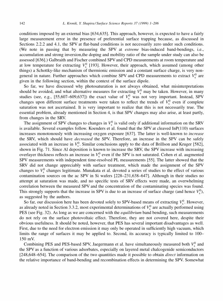
conditions imposed by an external bias [634,635]. This approach, however, is expected to have a fairlylarge measurement error in the presence of preferential surface trapping because, as discussed inSections 2.2.2 and 4.1, the SPV at ¯at-band conditions is not necessarily zero under such conditions.(We note in passing that by measuring the SPV at extreme bias-induced band-bendings, i.e.,accumulation and strong inversion,the doping and mobility ratio of the sample under study can also beassessed [636].) Galbraith and Fischer combined SPV and CPD measurements at room temperature andat low temperature for extracting V0
s [193]. However, their approach, which assumed (among otherthings) a Schottky-like mechanism of thermionic emission and a constant surface charge, is very non-general in nature. Further approaches which combine SPV and CPD measurements to extract V0
s aregiven in the following section, within the context of the surface dipole.
So far, we have discussed why photosaturation is not always obtained, what misinterpretationsshould be avoided, and what alternative measures for extracting V0
s may be taken. However, in manystudies (see, e.g., [55,607±609,637]) the exact value of V0
s was not very important. Instead, SPVchanges upon different surface treatments were taken to re¯ect the trends of V0
s even if completesaturation was not ascertained. It is very important to realize that this is not necessarily true. Theessential problem, already mentioned in Section 4, is that SPV changes may also arise, at least partly,from changes in the SRV.
The assignment of SPV changes to changes in V0s is valid only if additional information on the SRV
is available. Several examples follow. Koenders et al. found that the SPV at cleaved InP(110) surfacesincreases monotonously with increasing oxygen exposure [637]. The latter is well-known to increase
the SRV, which should have decreased the SPV. Therefore, an increase in the SPV can be safelyassociated with an increase in V0
s . Similar conclusions apply to the data of Brillson and Kruger [582],shown in Fig. 71. Since Al deposition is known to increase the SRV, the SPV increase with increasingoverlayer thickness re¯ects an increase in V0
s even if the SPV is not saturated. Cohen et al. augmentedSPV measurements with independent time-resolved PL measurements [55]. The latter showed that theSRV did not change appreciably with surface treatment, which made the assignment of the SPVchanges to V0
s changes legitimate. Munakata et al. devoted a series of studies to the effect of variouscontamination sources on the ac SPV in Si wafers [228±231,638±647]. Although in their studies noattempt at saturation was made, and no speci®c tests of SRV effects were made, an overwhelmingcorrelation between the measured SPV and the concentration of the contaminating species was found.This strongly supports that the increase in SPV is due to an increase of surface charge (and hence V0
s ),as suggested by the authors.
So far, our discussion here has been devoted solely to SPV-based means of extracting V0s . However,
as already noted in Section 3.3.2, most experimental determinations of V0s are actually performed using
PES (see Fig. 32). As long as we are concerned with the equilibrium band bending, such measurementsdo not rely on the surface photovoltaic effect. Therefore, they are not covered here, despite theirobvious usefulness. It should be noted, however, that PES has several important disadvantages as well.First, due to the need for electron emission it may only be operated in suf®ciently high vacuum, whichlimits the range of surfaces it may be applied to. Second, its accuracy is typically limited to 100±150 mV.
Combining PES and PES-based SPV, Jaegermann et al. have simultaneously measured both V0s and
the SPV as a function of various adsorbates, especially on layered metal chalcogenide semiconductors[248,648±654]. The comparison of the two quantities made it possible to obtain direct information onthe relative importance of band-bending and recombination effects in determining the SPV. Somewhat
142 L. Kronik, Y. Shapira / Surface Science Reports 37 (1999) 1±206

similarly, Alperovich et al. used photore¯ectance for quantitative and qualitative assessment of V0s and
SPV trends, respectively, upon Cs and O adsorption on GaAs(100) [254].A different interesting link between PES and SPV was established in recent years: Although
observed at times before that [655,656], in the early 1990s it has been systematically shown that PESresults may be in¯uenced by a parasitic surface photovoltaic effect [16±18]. Namely, the exciting UVor X-ray radiation source causes changes in the surface potential and therefore the measured band-bending is smaller than the true equilibrium value, possibly very signi®cantly. This is especially true atlow temperatures, where the SPV is more sizable in general. Neglecting to take this effect into accountcan lead to serious misinterpretations of experimental data. Therefore, a sizable body of literaturedevoted to observing this effect, correcting for it, and even exploiting it has evolved. A detaileddiscussion of the parasitic SPV effect is outside the scope of the present text. The interested reader isreferred to, e.g., [16±18,655±674] for further details. Similar parasitic SPV effects in photore¯ectance,i.e., an in¯uence of the probe beam on the band-bending, have also been noted. The reader is referred to[675,676] for a detailed discussion.
5.2.3. Surface dipole
In general, any surface chemical reaction can induce changes in both the surface band-bending, V0s ,
and the surface dipole, ��s. Both changes contribute to changing the surface work function, Ws (seeFig. 4 and Eq. (2.36)). Therefore, surface-induced changes in Ws can be expressed as:
�Ws � �V0s �����s�: (5.19)
Any changes in Ws can be measured with the Kelvin probe by detecting CPD differences before andafter surface reaction. In addition, V0
s can be measured before and after the reaction, either byphotosaturation or by any of the other means discussed in the preceding sub-section. Thus, ����s� canbe determined by simple subtraction using Eq. (5.19).
A few comments are in order. First, unlike the surface band-bending, the surface dipole is generallynot in¯uenced by illumination. This is because the inherently small width (ideally a monolayer) of thelatter and the strong bonding of its charge lead to its stability under external excitation [24]. Thus, SPVmeasurements are `blind' to ��s. It is this property which makes it possible to consider SPV-basedapproaches for extracting V0
s without having to worry about the surface dipole. Second, several authorsinterpreted treatment-induced Ws changes at GaAs [677,678], InP [679], and diamond [680,681]surfaces as being due to changes in the band-bending alone. While this may be true in some cases,surface dipole changes cannot be ruled out in the general case. Thus, such interpretation can be trustedonly if it accompanied by complementary evidence, e.g., of PES measurements [681]. Third, usuallyonly changes in ��s, rather than its absolute value, are sought. This is because, as explained inSection 2.1.4, the absolute value of ��s has to do with the value of the `ideal' (as opposed to thesurface) af®nity, �, which is almost always unknown. Fourth, the above-explained approach wasfrequently utilized by employing Kelvin probe and PES measurements for measuring �Ws and �V0
s ,respectively. A review of such studies may be found in [11]. Here, we naturally concentrate on studieswhich employed SPV measurements.
Combined SPV and work function measurements have been used in the context described above asearly as the 1960s by Campbell and Farnsworth, who studied the effects of oxidation on the band-diagram of CdS surfaces [609]. This approach was put to much use by Brillson et al. for their studies ofthe formation of metal-semiconductor interfaces, already mentioned in Section 5.2.1. An example of
L. Kronik, Y. Shapira / Surface Science Reports 37 (1999) 1±206 143

the evolution of the saturated SPV and the surface work-function (measured by a Kelvin probe) is givenin Fig. 71(b). When studying interfaces, rather than surfaces, Eq. (2.36) must be used with cautionbecause the overlayer may have both a surface and an interface dipole. Brillson et al. therefore assumedthat the magnitude of the interface dipole is best approximated by the �Ws ÿ�V0
s value found where�Ws is maximal (�1/2 monolayer in the case shown in Fig. 71(b). This is because the distinctionbetween surface and interface is not in effect yet for such thin overlayers. Using this approach, Brillsonet al. detected signi®cant changes in both SPV and CPD evolution between, e.g., the Al/GaAs and theAl/CdS interfaces [580], or the Al/ZnO and the Au/ZnO interfaces [583]. These differences werecorrelated with signi®cant differences in the chemistry of III±V versus II±VI semiconductors and ofreactive versus unreactive metals, respectively.
One of the key arguments against Brillson's claims of achieving photosaturation was that themeasured V0
s values in Fig. 71(b) do not yield the correct Schottky barrier height of the Al/GaAsinterface (with a similar problem in other interfaces as well) [614]. Interestingly, the sum of the SPV-measured V0
s and the interface dipole did yield the correct barrier height [615] This is intriguing sincein the abrupt metal/semiconductor band-diagram, shown in Fig. 7, the Schottky barrier height shouldnot depend explicitly on the interface dipole. This independence, easily con®rmed graphically fromFig. 7(b), is also physically reasonable because the abrupt interface dipole should be transparent toelectron tunneling and therefore should not pose a barrier to transport [614]. Brillson suggested that theinterface dipole is not atomically abrupt, but is still insensitive to illumination, due to a high density ofstates associated with the local charge redistribution [582]. A more detailed discussion of the truenature of this interface is outside the scope of the present text. It is interesting to note, however, that asomewhat similar argument was used by Jaegermann et al. to explain an SPV which was much smallerthan that anticipated from the band bending at the Cu/p-WSe2(0001) interface [651]. There, it is arguedthat Cu intercalation may result in a thin near-surface layer which contributes to the band-bending, butnot to the SPV.
A combination of CPD and saturated-SPV measurements was used in recent years by Cahen et al. fordeducing the systematic effects of various organic ligands to semiconductor surfaces on the band-bending and surface dipole at CuInSe2 [50,51,54], CdTe [50,51,55,56], CdSe [52], GaAs [53], and Si[57] surfaces. Organic ligands are an attractive alternative to the inorganic treatments usually used forsurface control. This is because organic ligands feature structural versatility and ¯exibility, may bedesigned to incorporate several properties simultaneously, and potentially allow systematicmodi®cations of one speci®c property independent of the others [54,56].
As an illustrative example of the above concepts, consider the modi®cation of a CdTe surface uponadsorption of dycarboxylic acid derivatives which include a polar group, consisting of para-subsitutedphenyl rings [56]. Fig. 74(a) shows that the changes in the surface dipole are linearly correlated to theaverage dipole moment of the ligand polar group. A linear correlation between the change in surfacedipole and the dipole moment of the adsorbed ligands, expected from Eq. (2.39), was found in all casesstudied. However, when ligand molecules more complicated than simple benzoic acids were used, aconstant offset, not predicted by this equation, was also found. This offset was attributed to anadditional dipole moment due to the binding group of the ligands and/or to the dipole due to the bondformed between the surface and the ligand. The latter can often be calculated from knowneletronegativities [54]. Fig. 74(b) shows that changes in the band-bending at the same surface arerelated to the position of the lowest unoccupied molecular orbital (LUMO) of the phenyl substituents.The closer the energy position of the LUMO to the CdTe surface states, the stronger is the molecule±
144 L. Kronik, Y. Shapira / Surface Science Reports 37 (1999) 1±206
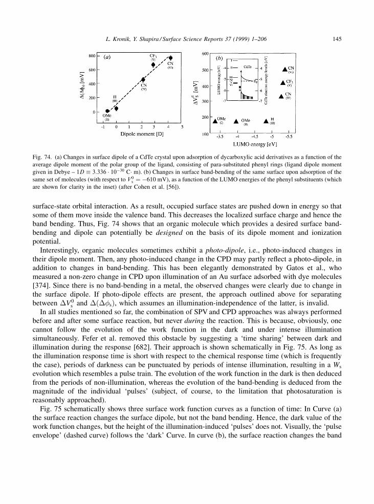
surface-state orbital interaction. As a result, occupied surface states are pushed down in energy so thatsome of them move inside the valence band. This decreases the localized surface charge and hence theband bending. Thus, Fig. 74 shows that an organic molecule which provides a desired surface band-bending and dipole can potentially be designed on the basis of its dipole moment and ionizationpotential.
Interestingly, organic molecules sometimes exhibit a photo-dipole, i.e., photo-induced changes intheir dipole moment. Then, any photo-induced change in the CPD may partly re¯ect a photo-dipole, inaddition to changes in band-bending. This has been elegantly demonstrated by Gatos et al., whomeasured a non-zero change in CPD upon illumination of an Au surface adsorbed with dye molecules[374]. Since there is no band-bending in a metal, the observed changes were clearly due to change inthe surface dipole. If photo-dipole effects are present, the approach outlined above for separatingbetween �V0
s and ����s�, which assumes an illumination-independence of the latter, is invalid.In all studies mentioned so far, the combination of SPV and CPD approaches was always performed
before and after some surface reaction, but never during the reaction. This is because, obviously, onecannot follow the evolution of the work function in the dark and under intense illuminationsimultaneously. Fefer et al. removed this obstacle by suggesting a `time sharing' between dark andillumination during the response [682]. Their approach is shown schematically in Fig. 75. As long asthe illumination response time is short with respect to the chemical response time (which is frequentlythe case), periods of darkness can be punctuated by periods of intense illumination, resulting in a Ws
evolution which resembles a pulse train. The evolution of the work function in the dark is then deducedfrom the periods of non-illumination, whereas the evolution of the band-bending is deduced from themagnitude of the individual `pulses' (subject, of course, to the limitation that photosaturation isreasonably approached).
Fig. 75 schematically shows three surface work function curves as a function of time: In Curve (a)the surface reaction changes the surface dipole, but not the band bending. Hence, the dark value of thework function changes, but the height of the illumination-induced `pulses' does not. Visually, the `pulseenvelope' (dashed curve) follows the `dark' Curve. In curve (b), the surface reaction changes the band
Fig. 74. (a) Changes in surface dipole of a CdTe crystal upon adsorption of dycarboxylic acid derivatives as a function of the
average dipole moment of the polar group of the ligand, consisting of para-substituted phenyl rings (ligand dipole moment
given in Debye ± 1D � 3:336 � 10ÿ30 C� m). (b) Changes in surface band-bending of the same surface upon adsorption of the
same set of molecules (with respect to V0s � ÿ610 mV), as a function of the LUMO energies of the phenyl substituents (which
are shown for clarity in the inset) (after Cohen et al. [56]).
L. Kronik, Y. Shapira / Surface Science Reports 37 (1999) 1±206 145
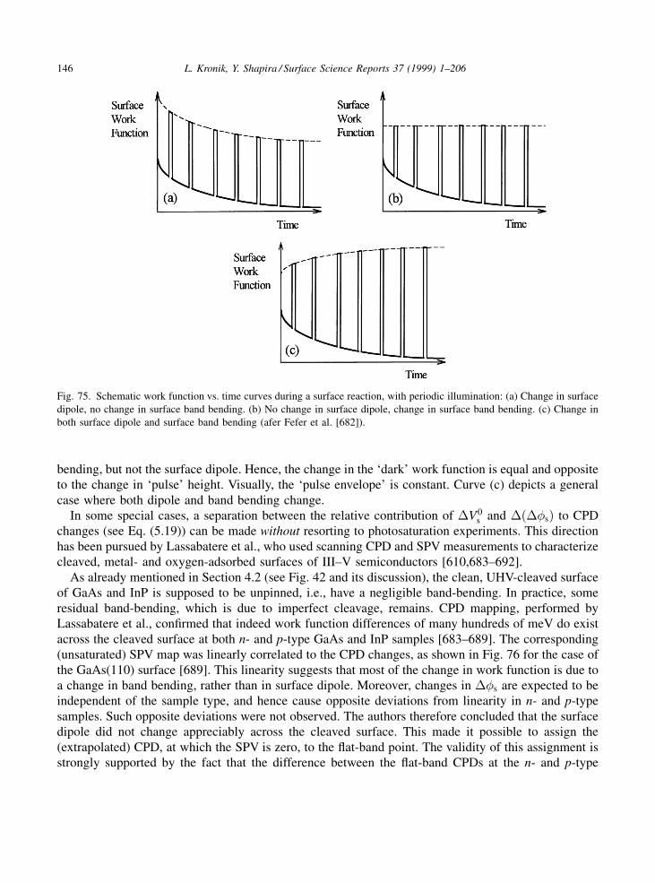
bending, but not the surface dipole. Hence, the change in the `dark' work function is equal and oppositeto the change in `pulse' height. Visually, the `pulse envelope' is constant. Curve (c) depicts a generalcase where both dipole and band bending change.
In some special cases, a separation between the relative contribution of �V0s and ����s� to CPD
changes (see Eq. (5.19)) can be made without resorting to photosaturation experiments. This directionhas been pursued by Lassabatere et al., who used scanning CPD and SPV measurements to characterizecleaved, metal- and oxygen-adsorbed surfaces of III±V semiconductors [610,683±692].
As already mentioned in Section 4.2 (see Fig. 42 and its discussion), the clean, UHV-cleaved surfaceof GaAs and InP is supposed to be unpinned, i.e., have a negligible band-bending. In practice, someresidual band-bending, which is due to imperfect cleavage, remains. CPD mapping, performed byLassabatere et al., con®rmed that indeed work function differences of many hundreds of meV do existacross the cleaved surface at both n- and p-type GaAs and InP samples [683±689]. The corresponding(unsaturated) SPV map was linearly correlated to the CPD changes, as shown in Fig. 76 for the case ofthe GaAs(110) surface [689]. This linearity suggests that most of the change in work function is due toa change in band bending, rather than in surface dipole. Moreover, changes in ��s are expected to beindependent of the sample type, and hence cause opposite deviations from linearity in n- and p-typesamples. Such opposite deviations were not observed. The authors therefore concluded that the surfacedipole did not change appreciably across the cleaved surface. This made it possible to assign the(extrapolated) CPD, at which the SPV is zero, to the ¯at-band point. The validity of this assignment isstrongly supported by the fact that the difference between the ¯at-band CPDs at the n- and p-type
Fig. 75. Schematic work function vs. time curves during a surface reaction, with periodic illumination: (a) Change in surface
dipole, no change in surface band bending. (b) No change in surface dipole, change in surface band bending. (c) Change in
both surface dipole and surface band bending (afer Fefer et al. [682]).
146 L. Kronik, Y. Shapira / Surface Science Reports 37 (1999) 1±206
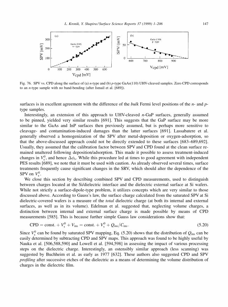
surfaces is in excellent agreement with the difference of the bulk Fermi level positions of the n- and p-type samples.
Interestingly, an extension of this approach to UHV-cleaved n-GaP surfaces, generally assumedto be pinned, yielded very similar results [691]. This suggests that the GaP surface may be moresimilar to the GaAs and InP surfaces then previously assumed, but is perhaps more sensitive tocleavage- and contamination-induced damages than the latter surfaces [691]. Lassabatere et al.generally observed a homogenization of the SPV after metal-deposition or oxygen-adsorption, sothat the above-discussed approach could not be directly extended to these surfaces [683±689,692].Usually, they assumed that the calibration factor between SPV and CPD found at the clean surface re-mained unaltered following deposition/adsorption. This made it possible to assess treatment-inducedchanges in V0
s , and hence ��s. While this procedure led at times to good agreement with independentPES results [689], we note that it must be used with caution. As already observed several times, surfacetreatments frequently cause signi®cant changes in the SRV, which should alter the dependence of theSPV on V0
s .We close this section by describing combined SPV and CPD measurements, used to distinguish
between charges located at the Si/dielectric interface and the dielectric external surface at Si wafers.While not strictly a surface-dipole-type problem, it utilizes concepts which are very similar to thosediscussed above. According to Gauss's law, the surface charge calculated from the saturated SPV at Sidielectric-covered wafers is a measure of the total dielectric charge (at both its internal and externalsurfaces, as well as in its volume). Edelman et al. suggested that, neglecting volume charges, adistinction between internal and external surface charge is made possible by means of CPDmeasurements [585]. This is because further simple Gauss law considerations show that:
CPD � const:� V0s � Vins � const:� V0
s � Qins=Cins: (5.20)
Since V0s can be found by saturated SPV mapping, Eq. (5.20) shows that the distribution of Qins can be
easily determined by subtracting CPD and SPV maps. This approach was found to be highly useful byNauka et al. [506,588,590] and Lowell et al. [594,598] in assessing the impact of various processingsteps on the dielectric charge. Interestingly, an ostensibly similar approach (less scanning) wassuggested by Buchheim et al. as early as 1977 [632]. These authors also suggested CPD and SPVpro®ling after successive etches of the dielectric as a means of determining the volume distribution ofcharges in the dielectric ®lm.
Fig. 76. SPV vs. CPD along the surface of (a) n-type and (b) p-type GaAs(110) UHV-cleaved samples. Zero CPD corresponds
to an n-type sample with no band-bending (after Ismail et al. [689]).
L. Kronik, Y. Shapira / Surface Science Reports 37 (1999) 1±206 147
5.3. Recombination rates
Carrier recombination rates, both in the bulk (expressed in terms of the excess carrier lifetime, �) andat surfaces or interfaces (expressed in terms of the SRV), are extremely important for thecharacterization of semiconducting materials. Moreover, they are crucial for the design and analysisof semiconductor devices. In this section, we describe how SPV measurements can be used for theextraction of these important parameters.
The most obvious method for obtaining direct information on carrier recombination is to observe therelaxation of the SPV signal after switch-off of super-bandgap illumination. Such monitoring of theSPV decay provides a contactless alternative to conventional, contact-requiring PCD measurements. Inaddition, SPV monitoring is much simpler than contactless PCD versions, e.g., mPCD. This approachhas been suggested and used as early as 1957 by Johnsnon [4], who extracted the same lifetime fromSPV relaxation and PCD measurements on Ge samples. Interestingly, Johnson also measured the time-dependence of the SPV when the sample was illuminated from the back, in order to estimate thetransport time across the sample. This is, in a sense, a contactless analogue of the well-known Haynes±Shockley experiment [90].
Johnson used a MIS structure for measuring the SPV relaxation. This is because the response time ofKelvin probe, with is typically a fraction of a second (see Section 3.1), is clearly inappropriate forfollowing rapid transients. However, the minimum time resolution available with a MIS structure is�0.1 ms at best (see Section 3.1). This value is still too large for many semiconductors, especiallydirect-bandgap ones. Thus, Johnson's work was not followed by other scientists. Only in 1996, HlaÂvkaand SÏvehla attempted such measurements again, in the context of presenting improvements to thetemporal resolution of MIS structures, already discussed in Section 3.2 [216].
In an important extension of Johnson's approach, Long et al. monitored the SPV relaxation of aSi(111) sample using PES [249]. With a temporal resolution of tens of ns, these authors had nodif®culty in determining a bulk lifetime of 1.7 ms. Recently, Marsi et al. improved the temporalresolution of such experiments to a fraction of a ns [693]. This was achieved by using free electron laserillumination and synchrotron radiation, which are inherently synchronized, as the SPV excitation andmeasurement sources, respectively. We note in passing that the monitoring of signal relaxation atspeci®c photoemission energies [694,695] is strongly in¯uenced by SPV variations and serves as anindirect measure of typical relaxation times of the latter. However, such experiments are not strictlySPV measurements and are not discussed further here.
Just like PCD measurements, SPV relaxation curves involve both bulk and surface relaxationcontributions, with no straight-forward means of separating the two. In fact, this problem is more severein SPV than in PCD because the former is inherently more sensitive to surface effects. Surface effectsin SPV relaxation curves were indeed found by several groups: HlaÂvka and SÏvehla clearly demonstratedthe impact of surface-trapping effects on the SPV relaxation by showing that background illumination,which eliminated long relaxation times associated with surface trapping, reduced the apparent lifetimefrom 700 to 5 ms [216]. Long et al. found that the bulk-related SPV relaxation is followed by a long`tail' of surface-related relaxation [249]. Using numerical ®tting of the measured data, they were able touse this surface interference bene®cially for deducing the SRV at the measured Si(111) surface. Marsi etal. found that the SPV relaxation on the sub-nsec scale at Si(111)-(2�1) samples is non-monotonous[693]. This was attributed by them to band-bending ¯uctuations, brought about by the different rate ofcharge ¯ow to donor and acceptor surface states.
148 L. Kronik, Y. Shapira / Surface Science Reports 37 (1999) 1±206

The distinction between bulk and surface recombination rates from the observation of SPV relaxationcurves is dif®cult (both theoretically and experimentally). Therefore, several approaches which directly
yield one or the other have been suggested. For a rigorous extraction of the bulk carrier lifetime,Munakata et al. developed an approach which is based on frequency-resolved, rather than time-resolved, ac SPV measurements [696]. These authors have limited their studies to Si, where diffusionlengths are relatively long. They therefore assumed that the effective SCR-edge SRV, S (which is not tobe confused with the real SRV ± see below), is much higher than the diffusion velocity, D=L. By usinglow-absorption illumination, they were therefore able to use Eq. (2.71a) for the photocurrent density,Jph. They then used Eqs. (2.72) and (2.73) to express the SPV as:
SPV � JphZeff � Jph
1
1=Req � i!Ceq
� eI�1
1=Req � i!Ceq
� L�! � 0�����������������1� i!�p : (5.21)
A schematic, logarithmic scale drawing of the SPV versus frequency dependence, deduced fromEq. (5.21), is shown in Fig. 77(a) [696]. It features two `knees'. The ®rst, !a � 1=ReqCeq, is due to theeffective impedance term, and is usually dominated by the SCR capacitance. The second, !b � 1=� ,typically occurs at a higher frequency and can be used for direct determination of � .
The above-derived approach implicitly assumes that Req and Ceq are frequency-independent.However, Munakata et al. have observed that this is not necessarily true, especially in the presence of asigni®cant surface-state density [697,698]. Depending on sample properties, the above-describedapproach therefore ranged between being highly useful and completely useless, depending on theability to identify !a and !b from an experimental curve. An example of the latter case is shown inFig. 77(b) [697]. Even in this more dif®cult case, !b can still be extracted using a somewhat morecomplicated approach [697]. If high-absorption illumination, such that �L� 1, is used, Eq. (2.71b)
Fig. 77. (a) Schematic drawing of the SPV vs. modulation frequency (after Munakata et al. [696]). (b) Experimental SPV vs.
modulation frequency curves at a Si sample with many surface states: x's ± large �, circles ± small �, squares ± ratio of the two
SPVs (after Honma et al. [697]).
L. Kronik, Y. Shapira / Surface Science Reports 37 (1999) 1±206 149

can be used. The SPV is then given by:
SPV � JphZeff � eI1
1=Req � i!Ceq
: (5.22)
Dividing Eq. (5.21) by Eq. (5.22), we obtain:
SPV�small��SPV�large�� � const: � L�! � 0�����������������
1� i!�p ; (5.23)
i.e., the problematic impedance term is eliminated. As shown in Fig. 77(b), � can be accuratelydetermined from the SPV ratio even when no `knee'-points are discernible in the normal low-absorption SPV versus frequency plot.
More recently, the same basic approach has been extended towards high-speed measurement oflifetime distribution maps [227]. If the detailed SPV versus ! plot is recorded at several points, so thatthe general position of !a and !b is fairly well known, !b at all other locations can be calculated byinterpolation from the SPV at two frequencies only ± one such that !a < ! < !b, the other such that! > !b.
The lifetime extraction technique of Munakata et al. is subject to the same set of limitations(Eq. (5.7)) as Goodman's diffusion length extraction technique. This is because both are based on thesame equations, namely, Eqs. (2.60) and (2.61). Speci®cally, the obtained lifetimes have been shown tobe prone to back surface effects if the sample is not much thicker than L [699±701]. Moreover,calibration charts for converting the apparent � into the true one have been suggested [700], just like inL measurements.
While providing for an elimination of surface recombination contribution to the bulk recombinationrate, the frequency-resolved approach of Munakata et al. does not remove the temporal resolutionlimitation, from which Johnson's original approach has suffered. Both measurements utilize the MISstructure and are thus limited by the same time-constants. Thus, it is no surprise that most scientistshave preferred to extract � by determining L using Goodman's approach and the using the relationL � ������
D�p
.An interesting means of surpassing the time-resolution limitations of the measurement device by
utilizing the inherently non-linear dependence of the SPV on the illumination duration was suggestedby Hamers and Cahill [702]. When using pulsed illumination, the longer the delay between subsequentpulses, the more time the excess carriers have to relax and the smaller the ensuing SPV signal is. Usinga fast (ps) pulse train from a laser source, Hamers and Cahill measured the SPV as a function of pulseseparation. The obtained dependence contained all information about the transient processes, eventhough all measurements were taken under steady-state conditions! This approach has been used byHamers and Cahill only in the context of scanning probe microscopy and for extracting the lifetimeassociated with the junction impedance (i.e., 1=!a) at Si(111)±(7�7) surfaces. However, it isconceivable that with further research this elegant technique could be adapted to measurements of thebulk lifetime, using other experimental tools, in Si as well as in other materials.
We now turn our attention to techniques intended for extraction of the surface recombination rate.These can be broadly divided into methods which measure the effective SRV at the back SCR-edge, S(de®ned in Eq. (2.60)), and methods which measure the real SRV at the free semiconductor surface, s
(de®ned in Eq. (2.21)). Both SRVs are similar in the sense that they are de®ned as a ratio of carriercurrent to the excess carrier density. However, s relies on the surface recombination rate and excess
150 L. Kronik, Y. Shapira / Surface Science Reports 37 (1999) 1±206
carrier density (for either type of carrier), whereas S relies on the overall minority carrier current andexcess density at the back SCR-edge.
In order to get an idea on the relation between the minority carrier S and s, let us consider a p-typematerial, where we employ many of the simplifying assumptions used in previous developments: First,we neglect SCR generation-recombination processes, so that Jn�0� � Jn�w� (see Eq. (2.62)). Then:
S � Jn�w�e�n�w� �
Jn�0�e�n�w� �
es�n�0�e�n�w� � s � �n�0�
�n�w� : (5.24)
Using Eq. (2.8), Eq. (5.24) may be recast in the form:
S
s� �n�0��n�w� �
fexp ��Fn�0� ÿ EFi�0��=�kT�� ÿ 1gfexp ��Fn�w� ÿ EFi�w��=�kT�� ÿ 1g : (5.25)
If �n� ni, Eq. (5.25) is further reduced to:
S
s' exp
�Fn�0� ÿ Fn�w�� ÿ �EFi�0� ÿ EFi�w��kT
� �: (5.26)
Assuming that the region at x > w is quasi neutral, EFi�0� ÿ EFi�w� � eVs, where Vs is the non-
equilibrium surface potential. Using the QFL approximation, Fn�0� � Fn�w�. Inserting these relationsinto Eq. (5.26) yields a very simple result:
S
s� exp
eVs
kT
� �: (5.27)
Eq. (5.27) shows that, in general, S may be signi®cantly larger than s. Howland and Fonash studied therelation between S and s for a Schottky barrier [545]. (As discussed in Section 2.2.2, this requiresdifferent assumptions on the quasi-Fermi levels than those used for deriving Eq. (5.27).) These authorsstudied the S=s ratio for different Schottky barrier heights and concluded that S is, in general, not adirect measure of s, in agreement with our simple calculation. Furthermore, they theoretically studiedSCRs with a surface defect layer, so that generation/recombination processes in the SCR were includedin S. In this case, they concluded that S is not necessarily even a simple qualitative ®gure of merit forsurface quality. Thus, extraction of S and of s are discussed below separately.
Before proceeding to discuss quantitative procedures, we note that the sensitivity of the SPV to asurface defect layer is not necessarily a disadvantage. For example, Chiang et al. used SPVmeasurements in conjunction with successive electrochemical etching. This enabled them to determinethe width of the surface defective layer by measuring the etch depth for which the SPV signal stabilized[703]. It should be noted, however, that the magnitude of the SPV variations does not directly re¯ect thechanges in S. This is because, as already emphasized in Sections 4.2 and 5.2.1, the SPV is also sensitiveto the equilibrium surface band-bending, which also changes with etching.
The most common approach for quantitative extraction of S relies on measuring Goodman plots(discussed in Section 5.1) [12,232,233,428,506,509,628,704,705]. The value of S affects the slope ofthe Goodman plot used to extract L (in both the constant SPV and the linear SPV approaches), due to the�S� D=L�ÿ1
coef®cient in the dependence of �n�w� on I (Eq. (2.61)). Qualitatively, this is apparent in,e.g., Fig. 63 [425], where the slope of the I��� versus 1=���� curve increases with decreasing surfacequality. If D=L is known, then the slope ratio before and after some surface treatment can be directlytranslated into the S ratio before and after the same treatment [704].
L. Kronik, Y. Shapira / Surface Science Reports 37 (1999) 1±206 151

Lagowski et al. [12] noted that Eq. (5.18) show that if the surface band-bending is known, S and Lmay be extracted simultaneously, from the slope and intercept of a Goodman plot, respectively. Thisapproach has indeed been used successfully in several studies [12,428,506,509]. Speci®cally, Hoff et al.used scanning SPV and work function measurements for simultaneous wafer-scale maps of L, [Fe], V0
s ,Qins, and S, thus combining several approaches discussed above for comprehensive characterization ofsurface and bulk properties of Si wafers [506].
Faifer et al. suggested a novel approach to measuring S in samples which obey all limitations of theGoodman technique (Eq. (5.7)), except for limitation (5.7)d, i.e., L� l. As explained in Section 5.1,violation of the latter assumption causes an SPV to develop on the back surface of the wafer, ifilluminated from the front (and vice versa). By solving the continuity equation with the front and backeffective SRV boundary conditions (Eqs. (2.60) and (5.9), respectively), they have shown that:
SPVbf � const � If � Sf
�� D
� �; (5.28a)
SPVfb � const � Ib � Sb
�� D
� �; (5.28b)
where `f' (`b') refer to the front (back) surface and indexes `bf' (`fb') refer to the back (front) SPV dueto front (back) illumination. Thus, if the experimental setup is such that the front and back SPV can bemeasured independently (see Section 5.1), then S at both the front and back surface can be extractedfrom a `Goodman-like' plot of SPVbf or SPVfb, as a function of If or Ib, respectively. We note that themeasured Sb can then be used to calibrate the measurement of L, via Eqs. (5.10) and (5.11).
If Jph and �n�w� can be calculated and/or measured, S can be found directly from Eq. (2.69). Forexample, Lile used the simpli®ed formula of Eq. (2.71b) for Jph and estimated �n�w� using auxiliary C±V measurements in order to assess S at the InSb/In2O3 interface of an InSb-based MIS structure [74].More recently, Yan extracted Jph from the intercept of a ln �T � SPV� versus 1=T curve (Eq. (5.17)) and�n�w� from a solution of the continuity equation which is somewhat less restrictive than Eq. (2.61). Thelimitations of the latter analysis were already discussed in Section 5.2.2.
Many attempts at the extraction of the majority carrier s rely on the extraction of �s (from which scan be calculated), based on the Kamieniecki model for the ac SPV response, described in Eqs. (2.79) and(2.80). Because the real part of 1=Zeff�!� contains �s, the latter can be easily found by analyzing the realand imaginary components of the ac SPV response [625]. Measurements of �s are performed togetherwith w measurements in the surface charge pro®ler [235] mentioned in Section 5.2.2 and are also usedin detecting the effects of various cleaning procedures on the state of Si wafer surfaces [625±630].
A cursory version of �s measurements is already found in the work of Nakhmanson et al. [706], whostudied the dependence of both the real and imaginary parts of the SPV on the measurement frequency.It has been further developed by Ukah et al. [482], who also studied the dependence of the ac SPV onbias illumination. A somewhat different approach to the extraction of �s has been suggested byGoldfarb [707] as part of the surface charge analyzer, discussed in Section 5.4.1 below. He noted that inEq. (2.73), the SCR width, w, is assumed to be a constant. However, this is clearly a ®rst-orderapproximation because the illumination tends to reduce w. Since this reduction depends on the surfacerecombination (i.e., on �s), �s can be reliably extracted from the ac SPV dependence on the illuminationintensity. Goldfarb used �s measurements for comparing the surface quality of different Si wafers.Because �s also depends on Vs (Eq. (2.79)), a reliable quantitative comparison between different wafers
152 L. Kronik, Y. Shapira / Surface Science Reports 37 (1999) 1±206
is obtained only if all wafers are brought into a controlled Vs via application of a gate bias or anappropriate cleaning agent. The most convenient value for this controlled Vs is in the inversion regime,where the SPV signal is large and both �s and w are insensitive to the exact value of Vs [627,707].However, for qualitative monitoring of different trends, �s can be used even in the absence of inversion.
Several comments are in order: First, as already noted in Section 5.2.2, by using Eqs. (2.79) and(2.80) for extracting �s, we implicitly assume that the SCR capacitance is the dominant capacitanceterm in the ac-SPV response. This assumption should always be treated with caution. For example,Munakata has suggested that the SRV at strongly inverted Si wafers may actually be determined fromstudying the capacitance term which is due to the inversion layer, rather than the depletion layer [708].Second, we note that �s is sometimes erroneously referred to as the `minority carrier surfacerecombination lifetime' [625,707], although the development leading to Eq. (2.79) clearly shows �s tobe related to the majority carriers. The true minority carrier s can be extracted, along with L and w, fromGoodman plots where w � L (see Sections 5.1 and 5.2.1), assuming one has a suf®ciently detailed andappropriate model for the charge balance in the SCR [523].
Takahashi and Yoshita de®ned a surface time-constant different from �s, in the form � � �Qss=�eI�,where �Qss is the photo-induced change in surface charge, as a simple indicator of surface quality. Thismeasure is, of course, related to the SRV. However, in calculating �Qss Takahashi and Yoshita assumedthat SPV changes are only due to surface charge changes, i.e., that photo-induced changes in Qsc arenegligible. The theory in Section 2.2.2. and, e.g., Fig. 70, show that this is not necessarily the case,especially at high illumination intensities. Thus, this approach must be used with caution.
To conclude this section, we note that the different techniques surveyed here for the extraction of � ,S, and s, seem to have been developed independently with little interaction between the groupsinvolved. Thus, a comparative experimental study of the relative strengths and weaknesses of thedifferent approaches has yet to be performed. Here, we have outlined the major advantages anddisadvantages of the approaches from a theoretical standpoint.
5.4. Surface states
A key strength of SPV-based methods is their inherent sensitivity to surface states. In Section 4.2, wehave demonstrated how this is used for (mostly) qualitative surface state spectroscopy. In this section,we present quantitative SPV-based analyses, which make it possible to extract surface state energydistributions, as well as other properties (e.g., thermal and optical cross-sections). We also discuss howsurface gap states may be distinguished from bulk gap states.
5.4.1. Energy distribution
Many SPV-based methods for determining the surface state energy distribution, Nt�E� (de®ned inEq. (2.23b)), are based on determining Qss�EFs�, i.e., the dependence of the surface charge on theposition of the surface Fermi level. In order to understand why that is so, let us combine Eq. (2.11) withEq. (2.23b), which yields:
Qss � e
Z�Nd
t �E��1ÿ f �E�� ÿ Nat �E�f �E�� dE; (5.29)
where f �E� is the Fermi±Dirac distribution. We approximate the latter to be equal to one below thesurface Fermi level, EFs, and to zero above it (i.e., our calculation is accurate only in the limit of
L. Kronik, Y. Shapira / Surface Science Reports 37 (1999) 1±206 153

negligible absolute temperature). Then, Eq. (5.29) reduces to:
Qss ' e
Z 1EFs
Ndt �E� dE ÿ e
Z EFs
ÿ1Na
t �E� dE; (5.30)
which yields:
Ndt �EFs� � Na
t �EFs� � Nt�EFs� ' ÿ 1
e
dQss
dEjE�EFs
: (5.31)
Eq. (5.31) shows that Nt�E� can be measured at the energy range over which EFs can be swept. Byde®nition:
EFs � EFb � eV0s ; (5.32)
where EFb is the Fermi level in the quasi-neutral bulk (see, e.g., Fig. 4). At a ®rst glance, modifying V0s
via some surface treatment seems to be the obvious choice for changing EFs. However, this isunacceptable since one must change EFs without disturbing the electronic properties of the surface.Eq. (5.32) was used by Allen and Gobeli as early as 1962 for modifying EFs via using samples withdifferent EFb [710]. By studying both p- and n-type samples over the entire doping range available tothem, they were able to modify EFs at the clean Si(111) surface over a �0.2 eV range slightly belowmidgap. By calculating Qsc from Eq. (2.30) and using Qss � ÿQsc, they constructed a Qss � f �EFs�curve. Finally, Nt�E� over the probed energy range was determined using Eq. (5.31).
In the above analysis, the role of SPV measurements is limited to determining V0s using any of the
techniques discussed in Section 5.2. Allen and Gobeli did not actually use SPV measurements at all forthat purpose. Rather, they used a combination of work function and photoemission measurements[710]. Later, Yamagishi used the same approach in conjunction with photosaturation for a renewedstudy of (oxidized and nitridized) Si(111) surfaces [572]. In addition to using samples with differentdoping types and levels, Yamagishi also changed the measurement temperature over a wide range.Thus, he was able to extend the range over which Nt�E� was measured to �0.8 eV, situatedsymmetrically about midgap.
The above approach has only been used scantily [565,711]. This is because it has several signi®cantdisadvantages. First, for using a set of samples with different doping, one must assume that the surfacestate distribution is the same for all samples, within experimental error. Second, one must also assumethat the surface does not undergo any reconstruction (which may modify the surface state distribution)with decreasing temperature. However, detailed investigations of the temperature dependence of V0
s
revealed that such restructuring does take place at various semiconductor surfaces [566,568±570]. Last,but not least, the use of different samples and different temperatures requires many measurements (ofboth EFb and EFs) and is quite tedious. Therefore, an approach which makes it possible to obtain manyEFs values at the same sample was clearly called for.
In 1971, Lam suggested that the necessary modi®cation may be obtained by sweeping the gate biasof a MIS structure [712], i.e., by modulating EFs via the ®eld effect. As explained in Section 2.1.5, thesimple charge conservation rule, Qss � ÿQsc, is no longer valid in this case and a more elaborateanalysis must be used. By taking the differentials of Eqs. (2.40) and (2.42), we obtain [712]:
dQm � dQsc � dQss � 0; (5.33a)
dVG � dVins � dV0s : (5.33b)
154 L. Kronik, Y. Shapira / Surface Science Reports 37 (1999) 1±206
Inserting these differential relations, as well as Eq. (2.41), into Eq. (5.31) yields:
eNt�Vs� � Cins
dVG
dV0s
ÿ 1
� �� dQsc
dV0s
; (5.34)
where Nt�E� is related to Nt�Vs� using Eq. (5.32). Lam measured V0s using photosaturation for different
gate voltages. He then calculated the ®rst term in Eq. (5.34) by numerically deriving the obtainedV0
s � f �VG� dependence and the second term from Eq. (2.30) [712].Lam's SPV-based approach is essentially an extension of previous capacitance analyses [712].
However, it features several signi®cant advantages over traditional C±V methods. First, it may beperformed in a contactless manner (see below). Second, it is easily applicable to structures with thickinsulators, where C±V methods fail due to the decreased insulator capacitance [713]. Finally, it is easierto interpret than C±V data as it avoids frequency±dispersion dif®culties [714]. Interestingly, thedependence of the SPVon the gate bias in MIS structures as a function of different surfaces and/or priorillumination was used by Snitko to qualitatively detect changes in surface state distributions as early as1959 [715]. However, no attempt at quanti®cation was made in those early measurements.
Lam's approach has found several useful applications. First, Lam himself used his approach forstudying the in¯uence of different technological steps (e.g., oxidation temperature, annealingtemperature and ambient, type of furnace, etc.) on the distribution of gap states at the Si/insulatorinterface of various commercial MIS capacitors, based on both SiO2 and Si3N4 [716]. In all cases,reasonable agreement with ac conductance data (where that method was applicable) was obtained.Consequently, Flietner, Heilig, et al. extended the ®eld modulation approach to the study of free Sisurfaces and non-metallized Si/insulator interfaces by employing an `arti®cial' MIS structure (i.e., acontactless gate electrode ± see Section 3.2) in conjunction with SPV-based V0
s -determining methodsdiscussed in Section 5.2.2 [717]. For example, the analysis based on Eq. (5.34) has been applied to thestudy of HF and H2O treated Si(111) surfaces [717,718], Si(111)/lead-boro-alumino-silicate glass [713]and Si/porous Si [719], and mostly chemically [720±725] and electrochemically [714,726,727] H-terminated Si (111) surfaces. The same approach was used by Venger et al. to study the surface statedistribution at real Ge [568] and GaAs [569] surfaces.
As an illustrative example, consider the evolution of the surface state distribution with progressiveelectrochemical H-termination of n-Si(111), shown in Fig. 78(a) [726]. It is readily observed that thedensity of gap states decreases and that the state distribution shifts and widens with increasingelectrochemical treatment time. A striking correlation is found between the time at which changes inNt�E� are most dramatic and the time at which a pulse in the dark current of the electrochemical celloccurs, as shown in Fig. 78(b). This indicates that the surface response is indeed electro-chemical,rather than chemical.
The results shown in Fig. 78 are generally consistent with other investigations of Flietner et al.[717,718,720,721,723], as well as with the earlier analyses of Allen and Gobeli [710], Yamagishi [572],and Lam [716]. All of these show that well-passivated Si surfaces feature a `U-shaped' distribution ofsurface states, which is typically symmetric about midgap. This distribution is usually related tointrinsic defects, i.e., strained Si±Si bonds and dangling bonds, which are back-bonded to Si atoms only[722,728]. On the other hand, peaks in the surface state energy distribution are usually interpreted asindicating Si atoms with lower states of oxidation [728]. Thus, the transition from a narrow and largedensity of surface states, situated above midgap, to a wide, smaller, and symmetric distribution ofsurface states (Fig. 78(a)), clearly indicates the passivation of the Si(111) surface under study.
L. Kronik, Y. Shapira / Surface Science Reports 37 (1999) 1±206 155

In Lam's ®eld modulation approach, the minimum resolvable density of surface states is determinedby the opposing signs of the two additive terms on the right hand side of Eq. (5.34): dQsc=dV0
s is alwaysnegative (see Eq. (2.30)) and the ®rst term must therefore be always positive to result in a positiveNt�E�. If the terms are very close in value, the difference signal may be obscured by noise, resulting inan unreliable measurement. Lam calculated that if the difference between the two terms is taken as atleast 10% of dQsc=dV0
s , then the minimum resolvable density increases with decreasing doping, and is�1010 cmÿ2 eVÿ1 for a �1015 cmÿ3 doping level (at room temperature) [712]. Lam and Rhoderickhave also devised a second ®eld modulation, SPV-based Nt�E� determining tool, where the minimumresolvable density was smaller [716,729]. However, that approach, based on analysis of small-signalSPVs, assumed that all gap states only trap one type of free carriers ± a rather restrictive assumption.Thus, this second approach has not been in much use. In another variant of small-signal SPV analysis,Adamowicz and Kochowski [574] complemented SPV measurements with photoconductivity ones toplot the SPV/�n ratio versus temperature. By assuming a distribution of donor and acceptor stateswhich decay exponentially from midgap, they obtained a reasonable qualitative ®t with theexperimental data. However, this approach is not suitable for direct extraction of surface state energydistribution.
Just like the doping/temperature modulation approach, the ®eld modulation approach relies on SPVtools only in determining V0
s . Nevertheless, studies where other V0s -determining techniques mentioned
in Section 3.3.2 were utilized in conjunction with Eq. (5.34) were not reported until quite recently.Kwok et al. [730] and Kobayashi et al. [731] used PES analysis to probe semiconductor/dielectricstructures, where bias was applied either by electron charging or by a biasing a thin metallic overlayer,respectively. The main limitation of this approach has to do with the thickness of the dielectric. On theone hand, it must be thin enough to allow the semiconductor interface to be within the probing depth ofPES. On the other hand, it must be thick enough to avoid breakdown upon bias. For example, Kwok etal. found that reliable results could be obtained at the Si/SiO2 interface for SiO2 thicknesses of only�20±150 AÊ [730]. Electrore¯ectance has also been used successfully for determining the surface statedistributions at the GaAs/SiO2 interface [732]. There, the main limitation was the need for a speciali/n� GaAs structure.
Fig. 78. (a) Surface state distributions at the n-Si(111) surface, obtained after various interruption times of the dark current in
an electrochemical cell. (b) Dark current and minimal Nt�E� as a function of time (after Dittrich et al. [726]).
156 L. Kronik, Y. Shapira / Surface Science Reports 37 (1999) 1±206

We now consider the limitations of analyses based on EFs modulation by either doping/temperatureor by electric ®eld. The energy resolution with which Nt�E� can be determined is limited by thenegligible-temperature approximation underlying Eq. (5.31), which is the basis of all our quantitativeanalyses so far. Therefore, the energy resolution is only several kT at best [710,712]. This was vividlydemonstrated in the early work of Allen and Gobeli [710]. Based on a simple derivative of theexperimental Qss � f �EFs�, they have obtained a `U-shaped' (hyperbolic cosine) Nt�E� distribution overthe �0.2 eV range probed. However, using direct integration, Allen and Gobeli found that the sameQss � f �EFs� curve could be obtained from many other distributions, as long as the qualitative trend(increasing density of states away from the middle of the energy range probed) was maintained. Thesedistributions included two uniformly-distributed minibands, separated by �8kT, and two discretesurface states, separated by �6kT.
Both EFs-modulating approaches are expected to fail if the sample under study has an excessivedensity of either surface or bulk gap states. If the surface state density is very high, the surface Fermilevel will be pinned. Then, modi®cations of gate bias, temperature, or doping will only modify EFs byvery little, resulting in a very small energy range over which Nt�E� can be determined. For example,Kwok et al. had to settle for a qualitative investigation of the InP/silicon nitride interface because Fermilevel pinning precluded a quantitative analysis [730]. This immediately explains why most successfulinvestigations described so far were limited to unpinned Si surfaces. In addition, possible hysteresiseffects due to capture of charge in surface states must be taken into account when performingmeasurements as a function of gate bias [568,712,717]. If the bulk state density is very high, Qsc (andhence Qss) can no longer be calculated from Eq. (2.30) and more general expressions must be used (seeSection 2.1.3). These, however, require detailed knowledge of bulk state energy positions and densities,which is not necessarily available.
By studying Ge/Al2O3 interface states, Venger et al. demonstrated that even if EFs can be modi®ed byboth temperature and ®eld, the surface state energy distribution measured by the two techniques is notnecessarily identical [568]. They reasoned that the state density is lower in the temperature-basedmeasurements because the sample does not reach complete thermal equilibrium during thermal cycling.Instead, only the fast surface states (the density of which is lower) react. They further reasoned that theslow states probed by the ®eld modulation method are located slightly inside the Al2O3 ®lm, so thattunneling is required. This makes the measured density of states an effective one because the accessiblestates depend on the electric ®eld in the Al2O3 ®lm.
A different type of ®eld modulation tool, intended for the Si manufacturing industry, was introducedby Kamieniecki and dubbed `surface charge analysis' (SCA) [624]. Kamieniecki combined the ac-SPVapproach used in the surface charge pro®ler (SCP) for measuring the surface space charge capacitance(see Section 5.2.2) with gate-bias modulation. (Note that although it is somewhat more complex, theSCA precedes the SCP historically, for reasons given below). Kamieniecki used a fairly thick spacer(�10 mm) as the insulator in his `arti®cial' MIS structure, which required using fairly large biases(� 1000 V). As a result, any built-in potential drops on the insulator (e.g., due to the CPD betweenmetal and semiconductor) were negligible and the charge on the gate was given simply byQm � CinsVG. By modulating the gate bias, Kamieniecki was able to construct a complete w versus Qm
curve, extending over the accumulation, depletion, and inversion regimes.The Si/insulator interface state distribution is derived from the w versus Qm curve in a manner which
is similar to that of the Lam approach, but which is more simple: From the value of w, both Qsc and EFs
are easily calculated using Eqs. (2.32) and (2.33), respectively. Since Qm is directly obtained from the
L. Kronik, Y. Shapira / Surface Science Reports 37 (1999) 1±206 157
measurement, dQss can be immediately obtained from Eq. (5.33a) over any energy range dE andinserted into Eq. (5.31) for obtaining Nt�E�.
We note that SCA can yield additional important information other than the interface state charge.This is because it is, essentially, a contactless, non-destructive analogue of standard C±V analysis. Thisis highlighted by, e.g., ac-SPV measurements which were used in conjunction with algorithmsoriginally devised for capacitance measurements in order to deduce the spatial variation of the spacecharge density at Pt/a-Si:H samples [733]. Going back to crystalline Si wafers, the bulk type and dopingmay be easily obtained from the w versus Qm curve [624]. First, the type of the sample (p or n) isdetermined from the direction of the curve because for p- (n-)type samples, inversion is obtainedfor positive (negative) gate charge; Second, as already discussed in the context of the SCP and justlike in textbook C±V analysis (see, e.g., [25] and [30]), the doping level can be easily calculated fromthe maximal value of w. The induced charge necessary for obtaining ¯atband conditions is also easilyread off w versus Qm curves by identifying the cross-over between the depletion and accumulationregimes. We also note that the cross-over between different regimes can be identi®ed even using dcSPV (and corona-discharge-induced biasing) [734], but the possibilities for quantitative analysis aremore limited.
In all analyses so far, we have assumed that there is no ®xed charge in the insulator ± an assumptionwhich incorrect for industrial Si-based MIS structures. Fortunately, this does not affect the resultspresented because a ®xed, additive surface charge term (which can be lumped into Qss) does not modifythe Nt�E� ' dQss=dE calculation. It is reasonable to assume that if EFs is where the minimum of the`U-shaped' distribution is obtained (typically around midgap for passivated Si wafers), the net interfacestate charge is negligible, due to the symmetry of donor and acceptor states on the two sides of the`U-curve'. Thus, if the insulator is thick enough so that Qm can be determined directly, Qins is simplygiven by Qm ÿ Qsc. This type of calculation is usually performed in the context of SCA [624], but canused in conjunction with other means of determining Qsc [713,735].
SCA (`contactless C±V analogue') offers several advantages over the use of standard C±V analysis.This is because many dif®culties are encountered when attempting to apply the latter approach toindustrial monitoring of Si wafers [736]. The most important problem is that post-processing steps arerequired in order to fabricate test MIS structures on the Si wafer. This is time consuming and costly andcannot be performed regularly. Thus, problems may go undetected for several production lots.Moreover, the source of contamination and/or intrinsic defects may be obfuscated by the additionalprocessing steps and wafers with only native oxides cannot be studied using C±V analysis. Finally, inthe latter analysis the insulator charge inferred from the ¯at-band voltage is weighted [25], i.e., chargescloser to the Si/SiO2 interface are weighted more than those close to the SiO2/metal interface. In SCA,measurements do not require any further processing. Moreover, since the SiO2 layer is only a smallfraction of the total insulating spacer used, the measured charge is practically unweighted because all ofit is effectively very close to the Si/SiO2 interface.
Due to its advantages, SCA was introduced in 1989 by Kamieniecki [624] as a commercial tool[234]. In the same year, Kamieniecki and co-workers from Digital demonstrated its usefulness forstudying the effect of Si wafer cleaning [737] and of ambient air in®ltration [738] on surfacepassivation and oxide charge. Soon thereafter, Murali et al. of Intel published a comprehensive studywhich established SCA as a valid and useful technique for in-line monitoring of micro-contaminationand process-induced damage [736]. Ajuria et al. of Motorola directly compared SCA and C±Vmeasurements as methods for detecting ionic impurities in Si/SiO2 structures [739]. They concluded
158 L. Kronik, Y. Shapira / Surface Science Reports 37 (1999) 1±206

that the two do not necessarily yield the same results because the additional processing steps requiredfor the C±V analysis may modify the oxide charge. However, both techniques show the same trends insurface charge with respect to any process studied. Of the two tools, SCA was determined to be farmore sensitive and less erratic than C±V.
Today, SCA is a well-established industrial tool. Some notable recent publications of its use bysemiconductor manufacturing companies include: Studies of the activity of HF/H2O treated siliconsurfaces in ambient air [740] (Digital), Real time oxidation monitoring [741] and damage evaluation ofreactive ion etching [742] (IBM), evaluation of pre-cleaning effects on thermal oxide ®lms [743](Seiko-Epson), characterization of rapid thermally grown dielectrics [744,745] (Sharp), and in-linemonitoring of oxide charge [498] (SGS-Thomson).
Naturally, the SCA is not without disadvantages: It is not well-suited to the study of bare Si wafers,mostly due to surface-state-related hysteresis encountered in the w versus Qm curves [737]. In addition,the high bias required for its operation, as well as the mylar spacer used in the device, may modify thebare surface. These disadvantages are overcome by using the more simple surface charge pro®ler (seeSection 5.2.2), which does not use gate biases or spacers. Thus, the latter device can be easily used forthe study of bare surfaces, at the expense of sacri®cing some of the SCA capabilities.
For completeness, we note that in a different ac-SPV based approach, Shimizu et al. determined thesurface charge by analyzing the frequency dispersion of the ac-SPV and extracting the capacitanceterms which are due to interface states, instead of assuming that all capacitive response is due to thedepletion region [735]. If in doubt about the source of the effective capacitance in the ac-SPV response,studying the frequency±dispersion of the SPV signal before proceeding with quantitative analyses isalways a good idea.
We brie¯y describe a different tool for the distinction between ionic and surface-state charge atSi wafer surfaces ± the frequency dispersion of saturated-SPV measurements, as in Fig. 72(b)[509,586,595±601]. In Section 5.2.1, we have already noted that characteristic `knees' can be observedin the SPV versus frequency curves, which are associated with insuf®cient re-emission of trappedcharge in the dark. If all surface charge is ionic, this effect is absent and the frequency dispersion curveshould remain ¯at up to f � 1=�bulk. Any decrease in the SPV indicates a partial contribution of surfacetrapping, and hence surface states. If (and only if!) all surface charge is compensated by trapping, it canbe calculated from the difference of the SPV before and after the `knee'. This interpretation is indisagreement with that of Lowell et al. (see, e.g., [596]), who interpreted a ¯atter gradient at a `knee' asindicating that surface-state charge dominates over ionic charge.
All the methods reviewed in this sub-section so far relied on indirect modi®cation of the surface statepopulation, by means of temperature, electric ®eld, or super-bandgap illumination. In Section 4.2, wehave shown that direct excitation of surface states with sub-bandgap illumination has been verysuccessful in determining the approximate energy position of surface states. Thus, it seems natural toextend these methods for quantitative characterization of surface state distributions, by considering thederivative of the SPV signal with respect to the exciting photon energy. As already noted in Section 4.2,the inherent dif®culty with such an approach is that the sub-bandgap SPV signal is always affected byboth the density of states and the optical cross-section of the states, with the separation between the twobeing very problematic.
Kronik et al. demonstrated theoretically and experimentally that derivative sub-bandgap SPS can beused for extracting the surface state distribution, if the SPV signal is saturated at each photon energyused [603]. This typically requires the use of a high-intensity tunable source, e.g., a tunable laser.
L. Kronik, Y. Shapira / Surface Science Reports 37 (1999) 1±206 159
Consider, for example, a depleted n-type semiconductor surface, where the surface band-bending is dueto trapping of electrons in surface states. Let us assume that the surface states in question have non-negligible optical cross-sections only with the conduction band. A saturated SPV signal then indicatesthat all states whose energy separation from the conduction band is smaller than h� have been emptiedout. Then, any small change in the surface potential (i.e., an SPV), due to a small increase, ��h��, inthe incident photon energy, is due to the evacuation of an additional charge, �nt, whose excitationenergy is between h� and h� ���h��. In other words, the change in surface potential with increasingphoton energy must be attributed to changes in the density of states probed alone. Changes in theoptical cross-section (which re¯ects the probability of absorption) are made irrelevant because the stateis completely emptied out regardless of the value of the optical cross-section. Thus, the surface electrondensity over the energy range d�h�� is given by the simple relation:
dnt � nt�h� � dh�� ÿ nt�h��; (5.35)
where an independent measurement of V0s is required for calculating nt from Vs via the depletion
approximation expression, nt ����������������������2�nbjVsj=e
p. Then, Nt�E� can be obtained from nt�E� via the Fermi-
Dirac distribution. Note that the analysis of Kronik et al. shows that the derivative of the SPV does notre¯ect the surface state distribution even if the optical cross-section is constant, due to the square rootdependence of nt on Vs.
The chief advantage of this approach is that since it does not assume a negligible temperature, itsenergy resolution is much better than that of the previous approaches [603]. Another reason for theimproved accuracy is that due to the square root dependence on Vs, even relatively large errors indetermining V0
s are translated into small errors in nt. A signi®cant disadvantage, however, is that it isstrictly valid only for unipolar excitation. For optical interaction with both bands, Eqs. (2.13) and (2.18)show that a given surface state does not empty out at high illumination intensity. Rather, its populationreaches a steady-state value of nt � �nNt=��n � �p�. However, if this complication is ignored and theanalysis of Eq. (5.35) is pursued nevertheless, the results are still expected to approximate the truedistribution reasonably well because the dependence of the optical cross-section ratio on the photonenergy is very frequently weaker that that of the optical cross-section itself [603]. Thoroughinvestigations of this approach, or detailed comparisons with the other tools discussed in this section,have yet to be performed.
5.4.2. Properties
Apart from the surface state energy position (if discrete) or distribution (if continuous), many otherimportant surface state properties can be determined. These include the surface state density, Nt, itselectron (hole) density, nt (pt), its thermal cross-sections for electrons and holes, kn and kp, and itsoptical cross-sections for electrons and holes, �n and �p. (All quantities have been de®ned inSection 2.1.2). Many approaches for extracting surface state parameters from various SPVmeasurements, especially time-resolved ones, have been devised. These approaches can be broadlycategorized into two groups. The ®rst group involves direct excitation of the surface-states under studyvia sub-bandgap excitation. The second group involves indirect modi®cation of surface state populationvia trapping of free carriers induced by super-bandgap illumination. Many of the approaches given herecan be modi®ed to the study of bulk states, taking into account that the free carrier density is that of thebulk (or the SCR), rather than that of the surface.
160 L. Kronik, Y. Shapira / Surface Science Reports 37 (1999) 1±206

Lagowski et al. were the ®rst to use time-resolved SPV measurements for a quantitative extraction ofsurface state properties, soon after the introduction of SPS [110]. A typical transient SPV curve,obtained at a basal CdS surface, where some speci®c quantities pertinent to the analysis of Lagowski etal. are highlighted, is given in Fig. 79 [110].
Many analyses of transient curves as in Fig. 79 (including that of Lagowski et al.) make twosigni®cant assumptions. The ®rst assumption is that of unipolar excitation. Namely, transitionsinvolving minority carriers are neglected (see Section 2.2.3 above). We continue our discussionassuming an n-type material with electron transitions between the conduction band and the surfacestate. A similar analysis may be performed for hole transitions involving the valence band. The secondassumption is that all generation and recombination transitions are assumed to involve only one surfacestate.
Under these assumptions, it may seem at a ®rst glance as though kn and �n can be obtainedimmediately by ®tting the transient `light-on' and `light-off' curves with exponential curves. However,this is usually incorrect. To understand why, let us reconsider the unipolar rate equation (Eq. (2.81)),reproduced here for convenience:
dnt
dt� ÿgth
n ÿ goptn � rth
n � ÿ�optn Int ÿ cnn1nt � cn�Nt ÿ nt�ns: (5.36)
As opposed to the generation terms, the recombination term in the above equation is not proportional tothe surface state occupation. The reason is that ns, the electron (volume) density at the surface, dependson Vs (via Eq. (2.27)) in the case of the FQL approximation). Vs obviously changes during the SPVtransient, which makes Eq. (5.36) a non-linear differential equation.
Inspection of Eq. (5.36) shows that the `light-on' part of the transient SPV curve can yield the opticalcross-section only if the problematic recombination term (as well as the less problematic thermalgeneration term) are negligible with respect to the optical generation. This may require high-intensityillumination, depending on the �n=cn ratio. If the optical generation term can be made to dominate,then nt decreases with a time constant of �on
n � 1=��nI�, from which �n can be extracted. This approachwas used by Kronik et al. [746], who observed that in the initial part of the `light-on' SPV transient(where the excess carrier density was not very large), obtained at the CdTe(100) surface using high-intensity illumination, an exponential rise was indeed observed. Moreover, they ®tted the transient SPVcurve for several illumination intensities and obtained a �on
n which was inversely proportional to I, asappropriate.
The time-constant ®tted to the SPV curve can be equated with �onn only if the SPV is small enough to
assume that it is proportional to dnt. For example, combining the depletion approximation (square root)
Fig. 79. Sub-bandgap (h� '0.5 eV) transient SPV curve, obtained at a basal n-CdS surface. Speci®c quantities pertinent to
quantitative analysis are noted (after Lagowski et al. [110]).
L. Kronik, Y. Shapira / Surface Science Reports 37 (1999) 1±206 161
form of Eq. (2.30) with Eq. (2.23) yields [110]:
Vs � C1 ÿ n2t
C22
; (5.37)
where C1 is the contribution to the surface potential of other surface states (the charge of which wasassumed above to remain constant even under illumination), and C2 �
��������������2�nb=e
p. If C1 is negligible, the
SPV�t� curve can be converted to a nt�t� curve provided that V0s is known [603]. In any case, the
relation between the time-constants of the SPV�t� and nt�t� curves must be examined.In the `light-off' part of the SPV response, the recombination term in Eq. (5.36) dominates by
de®nition, so that the relaxation of the sub-bandgap SPV is not expected to be exponential. An elegantdemonstration of this non-exponential nature was given by Kuhlmann and Henzler, who studied sub-bandgap SPV transients at the Si(111) surface [747]. These authors de®ned a time-dependent relaxationtime-constant, ��t�, in the form:
��t� � ÿ SPV
d�SPV�=dt; (5.38)
which can be directly calculated from the experimental SPV decay curve. By plotting ��t� versus theSPV, they noticed that ��t� increases as the SPV decay proceeds. This observation is an immediateconsequence of the mathematical form of the recombination term in Eq. (5.36). As the SPV decays, thesurface barrier increases, so that ns is reduced, the surface recombination is slowed, and its effectivetime constant increases. Kuhlmann and Henzler further noted that ��t� did approach a constant valuetowards the end of the relaxation, where only a residual SPV (�0.1 mV) remained. This is alsoexpected from Eq. (5.36) because the deviation from the linearity of the equation, introduced by theSPV, may be neglected if the latter is much smaller than kT=e. Therefore, the constant value of ��t�,obtained towards the end of the SPV relaxation (if observed), can be used as a reliable indicator ofsurface recombination rates. Unfortunately, using Eq. (5.36), we obtain a relaxation time constant of�off
n � 1=cn�n1 � ns�. Thus, cn (and hence the thermal cross-section, kn � cn=vn ± see Eq. (2.17)) can beobtained only if ns can be estimated.
We now consider the approach suggested by Lagowski et al. for a complete extraction of surfacestate properties [110,748]. In the following, the superscripts `0' and `1' denote steady-state conditionsin the dark (i.e., equilibrium) and under illumination, respectively. Lagowski et al. measured V0
s
using photosaturation, so that V1s was also immediately known because, by de®nition, SPV � V1
s ÿ V0s .
They then built an additional set of equations for the remaining ®ve unknown surface state pro-perties of interest ± Nt, kn, �n, n0
t , n1t . Two equations for these quantities are obtained from the
steady-state solutions of Eq. (5.36) in the dark and under illumination, using the FQL approximation.They are:
�Nt ÿ n0t �nb exp
eV0s
kT
� �� n0
t Nc expEt ÿ Ec
kT
� �; (5.39a)
�nIn1t � cn�Nt ÿ n1
t �nb expeV1
s
kT
� �ÿ cnn1
t Nc expEt ÿ Ec
kT
� �: (5.39b)
Two more equations are obtained from the speci®c form of the Poisson equation used above, Eq. (5.37),in equilibrium and under steady-state illumination, which introduces a sixth unknown constant ± C1.
162 L. Kronik, Y. Shapira / Surface Science Reports 37 (1999) 1±206

Due to the additional unkown, two more equations, which must rely on the transient parts of the curvein Fig. 79, not used so far, must be introduced.
As both the `light-on' and the `light-off' transients are non-exponential, Lagowski et al. concentratedinstead on the measured slopes of the SPV curve, obtained immediately after switching the light on andoff (see Fig. 79). Inserting Eqs. (5.39) into the rate equation (Eq. (5.36)), and using the derivative ofEq. (5.37), they obtained:
dnt
dt
����t�t�
0
� ÿ C2
2jV0s j1=2
_dVs
dt
����t�t�
0
� ÿ�nn0t I; (5.40a)
dnt
dt
����t�t�
1
� ÿ C2
2 V1s
�� ��1=2
_dVs
dt
����t�t�
1
� �nn1t I; (5.40b)
where t�0 (t�1 ) refers to the time immediately after illumination switch-on (switch-off).By simultaneously solving Eqs. (5.37), (5.39) and (5.40), a complete characterization of the surface
state is obtained. This approach has indeed been used for the complete characterization of surface statesat CdS [110,362], GaAs [319], ZnO [401], CdSe [377] and CdTe [749] surfaces. Moreover, if the SPVtransients are analyzed at many different wavelengths, the dependence of the optical cross-section onthe photon energy can be constructed [378,623].
As always, the above analysis is not without limitations. When several surface states are detectedusing SPS, the assumption that each one may be selectively excited is very problematic. This casts asigni®cant doubt over the application of the algorithm in such cases and has probably limited the actualuse of the approach. Even if only one state is optically excited, other states may still in¯uence theresults via trapping of the excited carriers (see Section 2.2.3). We have shown theoretically that theanalysis can be extended by: [623] (a) replacing the constant C1 in Eq. (5.37) with a detailed accountingof all surface charge, (b) writing a rate equation of the form of Eq. (5.36) for each of the states involved,and (c) recording as many SPV transients as there are types of surface states. Thus, the properties of all
surface states may be extracted. Moreover, as C1 is eliminated from the equations, V0s may also be
determined along with the other parameters, resulting in yet another technique for its extraction. Thisextension has not been tested experimentally yet. As explained in Section 2.2.3, if surface transitionsinvolving the minority carriers are identi®ed in the SPV spectra (i.e., the unipolarity assumption isinvalidated), analytical results are dif®cult to obtain. Nevertheless, judging by the above developmentsit seems that the information can be extracted from a suf®cient number of SPV transients, with the aidof numerical simulations. This has not been performed yet either.
A different assumption behind the algorithm of Lagowski et al. is that steady-state conditions areindeed obtained in the dark and under illumination. If the surface states are in poor communication withthe bulk, this is not necessarily true. However, Balestra et al. have shown that the approach is easilyextended to this case by making the necessary modi®cations in the rate equation [748]. Experimentally,the success of the approach critically depends on the ability to obtain an accurate reading of the slopes.This explains why it has been mostly applied to II±VI compounds, where transients are typically slowenough to be followed with a Kelvin probe. If a MIS capacitor, or other faster approaches, are used, onemust ascertain that the illumination is chopped with a frequency low enough to retain the true steady-state value of the SPV.
L. Kronik, Y. Shapira / Surface Science Reports 37 (1999) 1±206 163

Several attempts at extracting the optical cross-section from steady-state sub-bandgap SPVmeasurements have also been reported. Musatov and Smirnov [338] suggested that if the SPV is smallenough, it is expected to be proportional to the photo-current, where the latter is simply equal to egopt
n .Assuming further that the population of the surface states is approximately constant, the dependence ofthe SPV on the photon energy is then expected to directly follow the dependence of �n on h�. Thisenables the measurements of the latter dependence, at least in arbitrary units. There are two verysigni®cant assumptions behind this approach. First, the surface state involved must be discrete, or someof the SPV may be due to an increase in the density of states accessible to excitation with increasingphoton energy (see Section 5.4.1). Second, the optical current is expected to re¯ect egopt
n only if
recombination can be neglected, which is a strong assumption. We also note that the �=k ratio has beenextracted from analyzing the dependence of the SPV on photon energy [296] or illumination intensity[113]. Note that this requires detailed knowledge on other parameters (e.g., defect density) and thus isnot very general.
We now consider the quantitative analysis of super-bandgap SPV data. In this case, the surface statesare not excited directly. Rather, their population is modi®ed via trapping of photo-induced excesscarriers from the bands. Accordingly, they are used mostly for assessing the thermal cross-section(which controls thermal generation and recombination), as well as the state energy position, which alsoin¯uences emission rates. Again, the most signi®cant algorithm has to do with the analysis of the SPVtransient. In many cases, the SPV relaxation is composed of a fast component, followed by muchslower `tail'. A typical example is shown in Fig. 80(a) [604]. The slow SPV tail can be explained asfollows [295,604,750±752]. During illumination, minority carriers, which are swept in the direction ofthe surface by the electric ®eld in the SCR, are trapped in surface states. The fast decay immediatelyafter illumination switch-off is due to electron-hole recombination in the bulk. In its wake, the trappedminority carriers must be emitted in order to re-establish thermal equilibrium. This is a much slowerprocess than inter-band recombination, resulting in the SPV `tail'.
If re-trapping of charge can be neglected, then according to Eq. (5.36), the typical time-constant ofthe slow SPV decay would be:
� � 1=cnn1; (5.41)
where again we assume electron emission with no loss of generality. Just like in the case of opticalemission of surface carriers, here too the assumption that recombination is negligible and the process ittruly exponential must be examined with caution. It is typically found that for times which are longcompared to the inter-band recombination, but at which a signi®cant re-trapping of charge has not takenplace yet, the SPV is indeed reasonably exponential, as shown in Fig. 80(a). Thus, � can indeed bede®ned and extracted.
The time constant � does not have to be extracted directly from time-resolved measurements.Alternatively, it may be found by performing frequency-resolved measurements, as in Fig. 72(b). Asdiscussed in Section 5.2.1, if the chopping frequency exceeds 1=� , trapped minority carriers are not re-emitted in the dark, so that the overall SPV is reduced. Thus, � may be found from the inverse ofcharacteristic knees in the SPV versus frequency curve. This approach has been used successfully withboth saturated [509],[586],[595±601] and non-saturated [294,295] SPV.
The direct monitoring of SPV relaxation transients is an extension of similar ideas commonly appliedfor characterizing bulk states [30]. In the latter case, the population of the bulk states is typically drivenaway from equilibrium using an electrical or optical pulse, and the charge emission process is followed
164 L. Kronik, Y. Shapira / Surface Science Reports 37 (1999) 1±206

by monitoring capacitance or current transients. Lagowski et al. [604,750] and independently Estrada[751] have suggested that the identi®cation of gap states based on the SPV transients may be facilitatedby the use of the `rate window' concept, known as deep level transient spectroscopy (DLTS) [30]. In`rate window' analysis, one monitors the difference signal:
SPV�t2� ÿ SPV�t1� � const � exp�ÿt2=�� ÿ exp�ÿt1=��� �; (5.42)
where t1 and t2 are pre-selected. It is easy to show that this difference signal is maximal when� � �t2 ÿ t1�= ln�t2 ÿ t1�. Therefore, characteristic peaks, indicating individual gap states, appear whent2 ÿ t1 is varied (typically keeping t2=t1 constant), as in Fig. 80(b), or when the temperature, and hence� , are varied for a ®xed t1 and t2, as in Fig. 80(c). Hybrid SPV-DLTS analysis was also usedsuccessfully in conjunction with a scanning MIS capacitor in order to detect gap state distributions inGaAs [750] and areas with different gap state characteristics in CdTe [753]. Recently, a high-resolutionSPV-DLTS map, using STM-based sensing of the SPV, was also demonstrated [754].
By inserting Eqs. (2.16) and (2.17), which express n1 and cn, respectively, into Eq. (5.41) andby explicitly expressing the thermal velocity, vn, in terms of temperature and electron mass, we
Fig. 80. (a) Super-bandgap transient SPV curve, obtained at an n-type GaAs wafer at room temperature. (b) DLTS analysis of
the SPV relaxation ± ®xed temperature, variable `rate window'. (c) DLTS analysis of the SPV relaxation ± ®xed `rate window',
variable temperature. (d) Thermal activation plot of the `tail' time-constant extracted from the SPV relaxation (after Lagowski
et al. [604,750]).
L. Kronik, Y. Shapira / Surface Science Reports 37 (1999) 1±206 165

obtain [30]:
1
�T2� nkn exp��Ec ÿ Et�=kT �; (5.43)
where n � vnNc=T2 � const. Thus, just like in conventional DLTS, a logarithmic plot of 1=��T2�versus temperature should yield a straight-line, as in Fig. 80(d), from which both the energy positionand the thermal cross-section of the gap state involved can be easily derived [295,604,750,751].
Several important comments on Eq. (5.41) are in order. First, it has been used successfully longbefore `rate window' concepts were introduced to SPV (see, e.g., [295]). Second, a similar analysis mayin principle be applied even if the surface states trap majority carriers. This case is less frequent sincemajority excess carries are typically swept away from the surface. However, they may still bepreferentially trapped, depending on the ratio between the electron and hole thermal cross-sections (seeSection 5.2.1). If that is indeed the case, the slow and fast components of the SPV relaxation must haveopposite signs, as in Fig. 73(a). Third, SPV±DLTS, like all SPV tools, is sensitive to both surface andbulk states. Accordingly, SPV±DLTS can be used as a contactless alternative to conventional DLTS.Fourth, the dependence of the steady-state SPV on temperature, using both super-bandgap [295,303]and sub-bandgap [294,295,303] illumination, is also frequently exponential and can be used to yield an`activation energy'. However, since the steady-state SPV depends on many factors, the precise physicalmeaning of this activation energy must be examined with caution. For example, if the SPV isproportional to the excess carrier density, it may indicate the activation energy of shallow acceptors[294]. If it is governed by the surface charge, it may indicate a surface state energy [303], etc. Fifth, asmentioned above, if carrier trapping during the slow SPV relaxation is not outright negligible,Eq. (5.41), and hence Eq. (5.43), cannot be used. It was shown that even in the presence of trapping thetransient might still be approximately exponential, albeit with a modi®ed � [755].
Liu and Ruda reported an interesting `pump-probe' two beam extension of transient SPV analysis,applied to the study of semi-insulating GaAs ®lms, where the Dember potential dominates the SPVresponse [755]. They noted that in the limit of a small-signal SPV, Eq. (2.92) reduces to:
SPV � kT
e��n ÿ �p� �n
�0
; (5.44)
so that the small-signal, Dember-related SPV is inversely proportional to the dark conductivity of thesample. If a simultaneous `optical bias' illumination pulse is applied, �0 shall re¯ect the conductivity ofthe sample under this illumination. Therefore, in this case SPV measurements can be used forcontactless monitoring of the photoconductivity.
Liu and Ruda have recorded the `light-on' and `light-off' response of the SPV signal to the(independent) optical bias illumination, as shown in Fig. 81(a). It is readily observed that the Dember-related SPV decays rapidly upon illumination, due to the sudden photo-induced increase inconductivity. However, its increase upon switch-off of the optical bias is much more gradual due tothe slow release of captured carriers. The ensuing activation energy of the process was determinedusing a ��T� plot. At some range of low temperatures, it has been found that after the optical bias isswitched-off, the SPV increases rapidly to a value which is much larger than that found before the biaswas applied and slowly decreases towards that value afterwards. This is shown in Fig. 81(b). As thisphenomenon cannot be explained using the trapping mode, it was interpreted in terms of an optically-induced metastable transformation of the EL2 defect, which decays thermally after bias switch-off.
166 L. Kronik, Y. Shapira / Surface Science Reports 37 (1999) 1±206
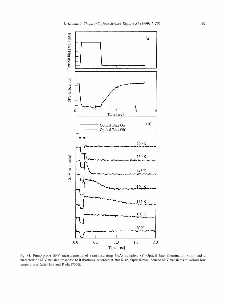
Fig. 81. Pump-probe SPV measurements of semi-insulating GaAs samples: (a) Optical bias illumination (top) and a
characteristic SPV transient response to it (bottom), recorded at 280 K. (b) Optical-bias-induced SPV transients at various low
temperatures (after Liu and Ruda [755]).
L. Kronik, Y. Shapira / Surface Science Reports 37 (1999) 1±206 167
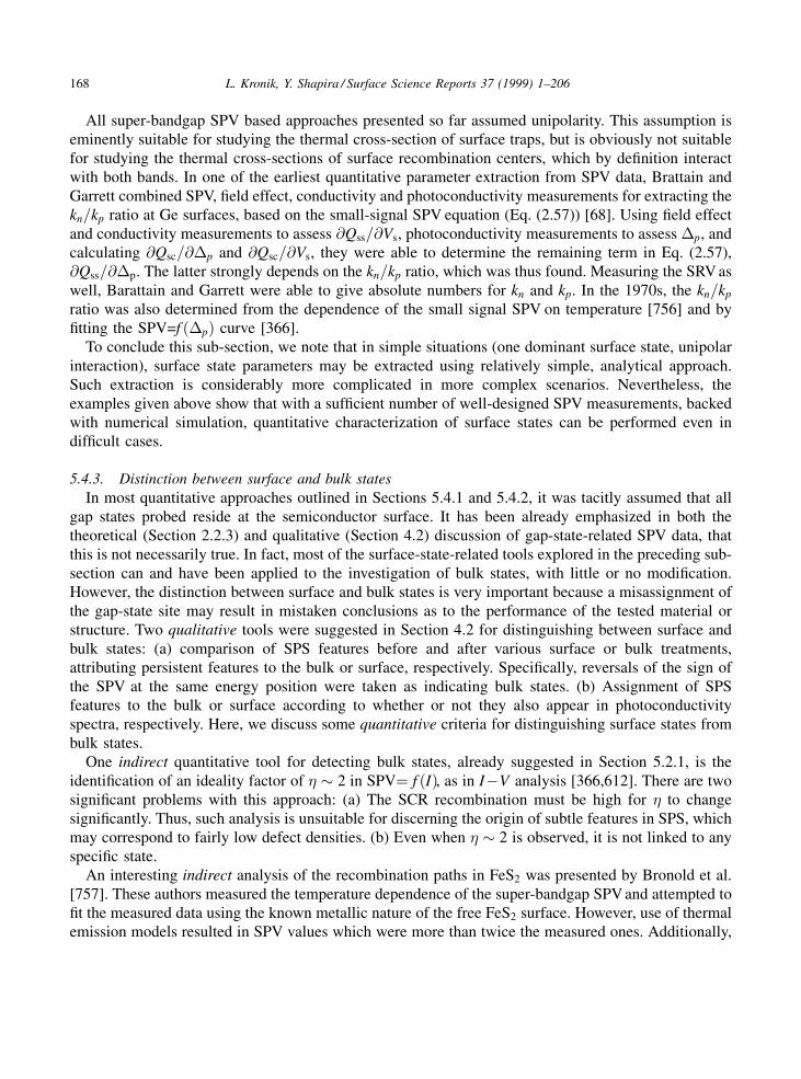
All super-bandgap SPV based approaches presented so far assumed unipolarity. This assumption iseminently suitable for studying the thermal cross-section of surface traps, but is obviously not suitablefor studying the thermal cross-sections of surface recombination centers, which by de®nition interactwith both bands. In one of the earliest quantitative parameter extraction from SPV data, Brattain andGarrett combined SPV, ®eld effect, conductivity and photoconductivity measurements for extracting thekn=kp ratio at Ge surfaces, based on the small-signal SPV equation (Eq. (2.57)) [68]. Using ®eld effectand conductivity measurements to assess @Qss=@Vs, photoconductivity measurements to assess �p, andcalculating @Qsc=@�p and @Qsc=@Vs, they were able to determine the remaining term in Eq. (2.57),@Qss=@�p. The latter strongly depends on the kn=kp ratio, which was thus found. Measuring the SRV aswell, Barattain and Garrett were able to give absolute numbers for kn and kp. In the 1970s, the kn=kp
ratio was also determined from the dependence of the small signal SPV on temperature [756] and by®tting the SPV=f ��p� curve [366].
To conclude this sub-section, we note that in simple situations (one dominant surface state, unipolarinteraction), surface state parameters may be extracted using relatively simple, analytical approach.Such extraction is considerably more complicated in more complex scenarios. Nevertheless, theexamples given above show that with a suf®cient number of well-designed SPV measurements, backedwith numerical simulation, quantitative characterization of surface states can be performed even indif®cult cases.
5.4.3. Distinction between surface and bulk states
In most quantitative approaches outlined in Sections 5.4.1 and 5.4.2, it was tacitly assumed that allgap states probed reside at the semiconductor surface. It has been already emphasized in both thetheoretical (Section 2.2.3) and qualitative (Section 4.2) discussion of gap-state-related SPV data, thatthis is not necessarily true. In fact, most of the surface-state-related tools explored in the preceding sub-section can and have been applied to the investigation of bulk states, with little or no modi®cation.However, the distinction between surface and bulk states is very important because a misassignment ofthe gap-state site may result in mistaken conclusions as to the performance of the tested material orstructure. Two qualitative tools were suggested in Section 4.2 for distinguishing between surface andbulk states: (a) comparison of SPS features before and after various surface or bulk treatments,attributing persistent features to the bulk or surface, respectively. Speci®cally, reversals of the sign ofthe SPV at the same energy position were taken as indicating bulk states. (b) Assignment of SPSfeatures to the bulk or surface according to whether or not they also appear in photoconductivityspectra, respectively. Here, we discuss some quantitative criteria for distinguishing surface states frombulk states.
One indirect quantitative tool for detecting bulk states, already suggested in Section 5.2.1, is theidenti®cation of an ideality factor of � � 2 in SPV� f �I�, as in IÿV analysis [366,612]. There are twosigni®cant problems with this approach: (a) The SCR recombination must be high for � to changesigni®cantly. Thus, such analysis is unsuitable for discerning the origin of subtle features in SPS, whichmay correspond to fairly low defect densities. (b) Even when � � 2 is observed, it is not linked to anyspeci®c state.
An interesting indirect analysis of the recombination paths in FeS2 was presented by Bronold et al.[757]. These authors measured the temperature dependence of the super-bandgap SPV and attempted to®t the measured data using the known metallic nature of the free FeS2 surface. However, use of thermalemission models resulted in SPV values which were more than twice the measured ones. Additionally,
168 L. Kronik, Y. Shapira / Surface Science Reports 37 (1999) 1±206

if SCR recombination was included, a ®tting of the temperature dependence was obtained only for abandgap value of about half its true size. Bronold et al. have therefore suggested that due to the defectchemistry of the FeS2 surface, there exists a thin surface layer which is effectively very highly doped.Thus, they have suggested that the results may be rationalized only if excess carriers are lost via bothSCR recombination and tunneling across the thin, highly-doped surface barrier. While elegant, thisanalysis is clearly case-speci®c.
It is reasonable to expect that for obtaining more direct information on the site of the state, thepopulation of the state must be modi®ed via direct excitation. Let us examine the quantitative differencebetween such charge modi®cation in surface and in bulk states: In the depletion approximation, acombination of Eqs. (2.24), (2.32) and (2.33) yields Vs � ÿQ2
ss=�2���. Thus, if the illumination inducesa surface and bulk change of �Qss and ��, respectively, the SPV is given by:
SPV � ÿ 1
2�
�Q0ss � �Qss�2�0 � �� ÿ �Q
0ss�2�0
" #; (5.45)
where the index `0' denotes equilibrium, as usual. If the illumination modi®es only the surface chargeor the bulk charge, Eq. (5.45) can be further reduced to:
SPV � ÿ �Qss�2Q0ss � �Qss�
2��0
; for fixed bulk charge; (5.46a)
SPV � �Q0ss�2��
2��0��0 � ��� ; for fixed surface charge: (5.46b)
Leibovitch et al. suggested that Eqs. (5.46) can be used as a basis for distinction between surface andbulk states, by relying on the dependence of the SPV on illumination intensity [116]. Their argumentsfollow. Whereas in Eq. (5.46a) the SPV � f ��Qss� dependence is super-linear, the SPV � f ����dependence in Eq. (5.46b) is sub-linear. Since the dependence of �Qss and �� on I, the illuminationintensity, may itself be sub-linear, the overall SPV � f �I� dependence may be sub-linear even in thecase of surface excitation. Thus, observation of a sub-linear SPV � f �I� dependence does not tell usanything about the surface state site. However, identi®cation of a super-linear dependence, even over alimited portion of the SPV � f �I� curve, is a de®nite indicator of surface states. For con®rming thisapproach experimentally, Leibovitch et al. compared the SPV � f �I� curve of a device grade InPsample with a damaged surface (which is dominated by surface states) with the SPV � f �I� curve of aFe-doped sample, dominated by bulk states, as shown in Fig. 82. A super-linear response is clearlyobserved for the surface states, but not for the bulk states, as appropriate.
In a somewhat similar approach, Lagowski et al. suggested earlier that Eqs. (5.46) can be used forsite assignment based on monitoring the super-bandgap SPV transient curve [604]: due to the squaredependence of the SPV on �Qss in the case of surface excitation, an exponential decay of nt due tocarrier emission, with a time constant of � , would result in both � and �=2 exponential components inthe SPV curve. Conversely, only a � component would be observed in the case of bulk excitation, due tothe lack of a non-linear term.
Leibovitch et al. have further suggested that the high intensity end of the sub-bandgap SPV� f �I�curve can also be used for site assignment [116]. For bulk states, the shift of the SCR edge withincreasing illumination is expected to modify the density of bulk states accessible to excitation which
L. Kronik, Y. Shapira / Surface Science Reports 37 (1999) 1±206 169
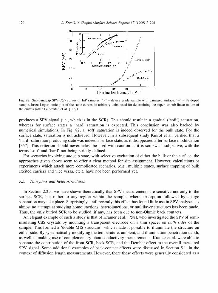
produces a SPV signal (i.e., which is in the SCR). This should result in a gradual (`soft') saturation,whereas for surface states a `hard' saturation is expected. This conclusion was also backed bynumerical simulations. In Fig. 82, a `soft' saturation is indeed observed for the bulk state. For thesurface state, saturation is not achieved. However, in a subsequent study Kinrot et al. veri®ed that a`hard'-saturation producing state was indeed a surface state, as it disappeared after surface modi®cation[357]. This criterion should nevertheless be used with caution as it is somewhat subjective, with theterms `soft' and `hard' not being strictly de®ned.
For scenarios involving one gap state, with selective excitation of either the bulk or the surface, theapproaches given above seem to offer a clear method for site assignment. However, calculations orexperiments which attack more complicated scenarios, (e.g., multiple states, surface trapping of bulkexcited carriers and vice versa, etc.), have not been performed yet.
5.5. Thin ®lms and heterostructures
In Section 2.2.5, we have shown theoretically that SPV measurements are sensitive not only to thesurface SCR, but rather to any region within the sample, where absorption followed by chargeseparation may take place. Surprisingly, until recently this effect has found little use in SPV analyses, asalmost no attempt at studying homojunctions, heterojunctions, or multilayer structures has been made.Thus, the only buried SCR to be studied, if any, has been due to non-Ohmic back contacts.
An elegant example of such a study is that of Kramer et al. [758], who investigated the SPV of semi-insulating CdS crystals by mounting a transparent electrode on a thin spacer on both sides of thesample. This formed a `double MIS structure', which made it possible to illuminate the structure oneither side. By systematically modifying the temperature, ambient, and illumination penetration depth,as well as making use of complementary photoconductivity measurements, Kramer et al. were able toseparate the contribution of the front SCR, back SCR, and the Dember effect to the overall measuredSPV signal. Some additional examples of back-contact effects were discussed in Section 5.1, in thecontext of diffusion length measurements. However, there these effects were generally considered as a
Fig. 82. Sub-bandgap SPV=f�I� curves of InP samples. `�' ± device grade sample with damaged surface. `�' ± Fe doped
sample. Inset: Logarithmic plot of the same curves, in arbitrary units, used for determining the super- or sub-linear nature of
the curves (after Leibovitch et al. [116]).
170 L. Kronik, Y. Shapira / Surface Science Reports 37 (1999) 1±206

nuisance and suppressed as much as possible. SPV-based charge mapping at the buried interface ofsilicon-on-insulator wafers was mentioned in Section 5.2.1 [589].
Some signi®cant, yet isolated, SPV studies which were designed to study buried interfaces werepresented in the early 1980s [759±761] and are discussed in more detail below. However, aconcentrated effort at applying SPV measurements to the analysis of bi- and multi-layer structures wasmade only in the 1990s, mostly by the research group of the authors.
This section, which is devoted to the SPV analysis of ®lms and heterostructures, begins with adetailed discussion of the principles and capabilities of SPS analyses of multilayer structures. Thisdiscussion is followed by reviewing the applications of SPS to the study of quantum structures and byshowing how SPV measurements can be used for obtaining quantitative information on interface andheterostructure band diagrams.
Before proceeding, we note that it could be argued that the term `surface photovoltage' is no longerappropriate for a photovoltage related to buried interfaces. We shall nevertheless continue to use thisterm here because while the photovoltage is not necessarily generated at the surface, it is measuredthere.
5.5.1. Spectroscopy of multilayer structures
We start our discussion of the SPS of multilayer structures by considering an illustrative example,shown in Fig. 83. This ®gure features SPV spectra of a ZnO:Al/u-ZnO/CdS/Cu(In,Ga)Se2 layeredstructure, used for the fabrication of thin ®lm solar cells (`u' denotes unintentional doping) [402].Distinct spectral `knees' at �1 eV, �2.4 eV, and �3 eV, corresponding to the bandgaps of Cu(In,Ga)Se2
(CIGS), CdS, and ZnO, respectively, are clearly observed. The unequivocal identi®cation of all threebandgaps con®rms the above mentioned theoretical prediction of SPS sensitivity to buried interfaces(see Fig. 18).
While spectral `knees' are assigned to the various bandgaps as in the simple SPS analysis discussedin Section 4.1, the interpretation of the slope sign of these `knees' is considerably more complicatedthan that offered in Section 4.1. There, we have argued that, as long as the SPV can be associated witha decrease in surface band-bending and that the surface SCR is in depletion or inversion, positiveand negative super-bandgap SPVs necessarily correspond to n- and p-type materials, respectively. Inthe SPS of multi-layer structures, this simple rule is no longer necessarily valid for two distinctreasons.
Fig. 83. SPV spectra of ZnO:Al/u-ZnO/CdS/CIGS structures for various annealing times (after Gal et al. [402]).
L. Kronik, Y. Shapira / Surface Science Reports 37 (1999) 1±206 171
The ®rst reason for deviation from the type assignment rule of Section 4.1 can be easily understoodwith the aid of Fig. 18. In this ®gure, the n-type thin ®lm has two SCRs, related to the surface and theinterface, both of which are in depletion. However, a decrease of the surface band-bending results in apositive SPV (Fig. 18(a)), whereas a decrease in the interface band-bending results in a negative SPV(Fig. 18(b)). This is a direct result of the different direction of the band-bending in the two SCRs withrespect to the back contact. Therefore, an assignment of layer type which is based on the sign of theSPV slope can be made only if the dominating SCR can be identi®ed. For example, Moons et al.measured the SPV response of the organic/inorganic p-dithioketopyrrolopyrrole (DTPP)/SnO2:Fheterojunction [414]. They used both front- and back-side illumination, which selectively excited theDTPP/air and the DTPP/SnO2 depletion regions, respectively. Indeed, the SPV from the two depletionregions featured opposite signs, in agreement with the above explanation.
A special class of semiconductors, known as layered metal chalcogenides, feature basal planesurfaces which are free of dangling bonds and are therefore not expected to exhibit any band-bendingunder UHV conditions [762]. Consequently, the SPV of structures based on these materials should begoverned by their buried interfaces, rather than by their surfaces. This provides a particularly goodopportunity for experimentally con®rming the SPV signs expected from a back SCR. Such a study wasperformed by Lang et al., who investigated the SPV of GaSe/WSe2 structures under UHV conditions[762]. When studying the SPV of a p-GaSe/n-WSe2 structure as a function of overlayer thickness, Langet al. found a monotonously increasing positive SPV, attributed to the build-up of the depletion regionat the buried p±n heterojunction. The SPV sign is in agreement with the direction of the band-bendingat the buried depletion region and in disagreement with the SPV sign predicted for a depletion layer atthe surface of the p-type top layer, as expected.
An even more interesting evolution of the SPV was found by Lang et al. when studying the p-GaSe/p-WSe2 structure. After annealing (which is performed prior to GaSe growth), the surface regionof the p-WSe2 region is known to convert into n-type, so that the measured structure is really abipolar-transistor-like p-GaSe/n-WSe2/p-WSe2 structure. In this case, a negative SPV, interpreted to berelated to the buried n-WSe2/p-WSe2 homojunction, was found. The absolute value of this SPVdecreased with increasing overlayer thickness, due to the counteracting effect of the p-GaSe/n-WSe2
heterojunction, but the SPV sign was not inverted, indicating a dominance of the deeper junctionthroughout.
As the magnitude of equilibrium band-bending is not the only factor in¯uencing the SPV magnitude,the SPV-dominating SCR is not necessarily where the equilibrium band-bending is larger. This pointhas been recently demonstrated by Moons et al., who studied n- and p-type porphyrin semiconductinglayers which were (separately) deposited on Indium Tin Oxide (ITO) [413]. In this structure, twodepletion regions in the porphyrin layer can be expected: a front one, associated with the free surfaceand a back one, associated with the Schottky barrier between the porphyrin layer and the highlyconductive ITO. CPD measurements in the dark indicated an increase (decrease) of the surface workfunction of the porphyrin/ITO structure with increasing porphyrin p-type (n-type) overlayer thickness.This means that the CPD evolution is dominated by the increasing back depletion region, as dominationof the front one would result in the opposite CPD trend. Nevertheless, the SPV slope change signs at theporphyrin `bandgap' were found to be commensurate with a dominating band-bending reduction at thefront depletion region, for both types of porphyrins used. This was interpreted by assuming that therecombination rate at the back SCR is larger than that at the front SCR, so that the photovoltaic effect atthe back SCR is reduced. This conclusion was con®rmed by independent contact I±V measurements in
172 L. Kronik, Y. Shapira / Surface Science Reports 37 (1999) 1±206

the dark and under illumination, which yielded a very small photovoltage. Similar results were obtainedby Moons et al. at the p-DTPP/SnO2:F heterojunction [414].
The second possible reason for deviation from the type assignment rule of Section 4.1 has to do witha reduced photon ¯ux arriving at a buried SCR, due to partial absorption of light in the overlayer. Inorder to understand this effect, let us consider an extreme case where a certain layer absorbs light at itsbandgap energy, but produces no photovoltaic effect whatsoever because for some reason no chargeseparation can take place. If at energies lower than this bandgap, a photovoltaic effect is produced atsome region of the sample lying beneath this layer, then a decrease in the magnitude of the SPV will benoticed as soon as the layer begins to absorb. Thus, a `knee' associated with the layer bandgap will berecorded in the SPV spectrum, even though the layer has not produced any photovoltaic effect of itsown. Clearly, in this case the sign of the SPV slope change has nothing at all to do with the type of thelayer.
As an experimental demonstration of absorption-related SPS features, let us consider the `knees' ofFig. 83 in some more detail. Both the CdS and the ZnO layers are transparent to �1 eV photons, so thatthe latter have no dif®culty in getting to the CIGS region. At �1 eV, the absorbed photons produce apositive �CPD (negative SPV), due to the reduction of the band-bending at the n-CdS/p-CIGSheterojunction. The same mechanism is also responsible for the solar cell operation of the ZnO/CdS/CIGS structure. It is much more dif®cult, however, to explain the CdS-related feature at �2.4 eV insimilar terms: On the one hand, if the SPV were due to additional absorption of photons at the CdS/CIGS p±n junction, the �CPD slope change would be positive, rather than negative. On the other hand,it is not reasonable to attribute the observed negative slope change to a signi®cant depletion region atthe ZnO/CdS interface because the existence of such a depletion region would severely hinder the solarcell performance of the structure. A reasonable explanation, however, is that as the CdS layer begins toabsorb photons the effective photon ¯ux at the region of the sample where charges can be separated isreduced. This, in turn, reduces the magnitude of the SPV signal. This mechanism is even more clearlyat work near the ZnO bandgap, at �3 eV, where a drastic decrease of the SPV signal is observed. Afterthe ZnO bandgap, only a residual SPV which is independent of the photon energy remains. This isattributed to an incomplete relaxation of the CIGS-related SPV, due to non-steady-state conditionsduring the acquisition of the data. Thus, the agreement of the negative �CPD slope change signs at theCdS and ZnO bandgaps with the n-type nature of the CdS and ZnO layers seems to be coincidental,rather than re¯ecting a success of the type assignment scheme of Section 4.1.
Some recent SPV and SPS investigations of bi-layer structures have been devoted to thecharacterization of porous Si, using both contactless [308±312],[316],[763] and contact [313±315]measurements. Since porous Si is typically prepared by anodization of crystalline Si, a (porous-Si thin®lm)/(crystalline-Si substrate) structure is naturally formed. Accordingly, all SPS data of suchstructures revealed various features between �2 eV and �3 eV, related to the porous-Si layers, inaddition to the crystalline-Si related `knee' at �1.1 eV [308,310±316]. However, the sign of the porous-Si related features was found to vary, depending on the technological details of porous-Si anodizationand subsequent treatments [308].
In some of these studies [309±311], a complicated transient SPV behavior, including a non-monotonous relaxation of the SPV after illumination and relaxation times as long as several hours, wasobserved. This behavior, which is not found at surfaces of crystalline Si, indicates that signi®canttrapping processes take place in the porous-Si layer (as can be expected from the highly non-idealnature of this layer). As already argued in Section 4.1, this means that another mechanism for SPV
L. Kronik, Y. Shapira / Surface Science Reports 37 (1999) 1±206 173
generation, namely, preferential trapping, must also be taken into account and may even dominate overthe usual band-bending-related SPV. When this is the case, the sign of the SPV response is againunrelated to the semiconductor type (see Section 4.1). Due to the complicated transport phenomenaencountered at porous-Si layers, consensus has not been reached yet on the dominating SPV-generatingmechanism in porous-Si/crystalline±Si structures. In different studies, all mechanisms described abovehave been invoked to explain the various trends observed in the different ®lms studied. Thesemechanisms include the usual band-bending-related SPV (at both front and back SCRs) [311,315],preferential trapping at the porous-Si layer [311], and absorption at the porous-Si layer which reducesthe crystalline-Si-related SPV [313].
We emphasize that, as in Section 4.1, the sign of the SPV slope at the various `knees', rather thanthe sign of the SPV itself, must be analyzed. For example, Kashkarov et al. suggested that the inversionof the SPV sign at h� >3.2 eV, observed after heating a porous-Si/crystalline-Si layer which wasstored in air, re¯ected a change in the direction of electric ®eld in the porous layer [311]). However,since no change in SPV slope signs was observed following this treatment, this interpretation must berejected.
Throughout our discussion so far, we have implicitly assumed that the various SCRs in the structureare decoupled, namely, that the photovoltaic response in one SCR is independent of that of the otherSCRs. For two SCRs to be decoupled, they must be separated by a quasi-neutral region which is thickerthan both the Debye screening length, LD (de®ned in Section 2.1.3), and the diffusion length, L. Theformer assures that the two SCRs cannot in¯uence each other via electrostatic interaction. The latterassures that excess carriers cannot be injected from one SCR to the other. In semiconductors ofreasonable doping and quality L > LD, so that the diffusion length limitation is usually the more severeone. Mishori et al. have recently performed SPS measurements of a GaAs/AlGaAs heterojunctionbipolar transistor (HBT) structure, consisting of a graded n�-AlGaAs emitter on a p�-GaAs base, whichis itself on an n-GaAs collector [764]. This results in two depletion regions (emitter/base and base/collector) which feature opposite directions of band-bending. By design, a HBT structure must feature asigni®cant injection of charge from emitter to collector. Accordingly, Mishori et al., using numericalcalculations, have shown that the SPV spectrum undergoes signi®cant qualitative and quantitativemodi®cations with a changing electron mobility in the base (which changes the extent of chargeinjection between the two junctions). Thus, an explicit consideration of coupling effects is crucial forsuccessful quantitative interpretation of coupled SCRs, but may be signi®cant even for qualitativeanalyses if the coupling is substantial.
Karpovich et al. suggested an elegant experimental technique for separating between the back andfront SCR contributions by means of changing the position of the back contact [341]. To understandtheir approach, let us consider Fig. 18 again. We have already explained that in the absence ofsigni®cant Dember effects, the SPV measured at the semiconductor surface is an algebraic sum of theSPVs accumulated in the different SCRs between the surface and the back contact (see Section 2.2.5and the discussion of back-contact effects in Section 5.1). Usually, the back contact is in the physicalback of the sample so that the overall SPV is the sum of the SPVs due to both SCRs. However, if theback contact is placed on a non-illuminated edge of the front surface of the sample (and care is takenthat it is not reached by photons or excess carriers), the measured SPV is only due to the front SCR.This is because the SPV due to the buried SCR changes the potential of both the `back' and frontcontacts, so that it produces no net difference between them. The SPV due to the back SCR is theneasily obtained by subtracting the SPV measured with the `back' contact on the front side from the SPV
174 L. Kronik, Y. Shapira / Surface Science Reports 37 (1999) 1±206
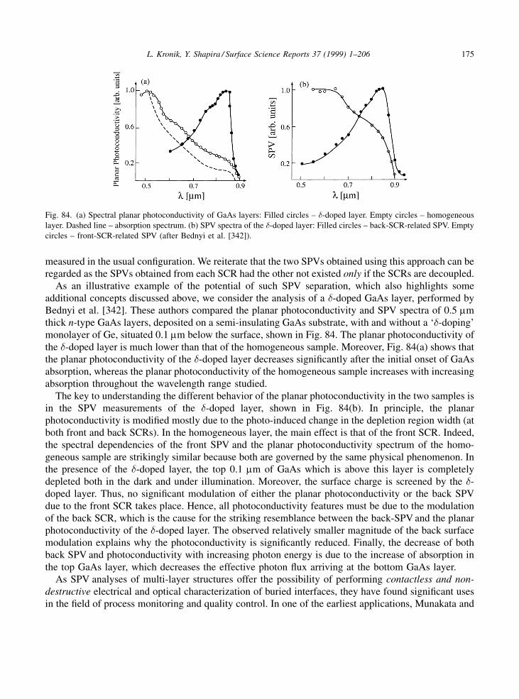
measured in the usual con®guration. We reiterate that the two SPVs obtained using this approach can beregarded as the SPVs obtained from each SCR had the other not existed only if the SCRs are decoupled.
As an illustrative example of the potential of such SPV separation, which also highlights someadditional concepts discussed above, we consider the analysis of a �-doped GaAs layer, performed byBednyi et al. [342]. These authors compared the planar photoconductivity and SPV spectra of 0.5 mmthick n-type GaAs layers, deposited on a semi-insulating GaAs substrate, with and without a `�-doping'monolayer of Ge, situated 0.1 mm below the surface, shown in Fig. 84. The planar photoconductivity ofthe �-doped layer is much lower than that of the homogeneous sample. Moreover, Fig. 84(a) shows thatthe planar photoconductivity of the �-doped layer decreases signi®cantly after the initial onset of GaAsabsorption, whereas the planar photoconductivity of the homogeneous sample increases with increasingabsorption throughout the wavelength range studied.
The key to understanding the different behavior of the planar photoconductivity in the two samples isin the SPV measurements of the �-doped layer, shown in Fig. 84(b). In principle, the planarphotoconductivity is modi®ed mostly due to the photo-induced change in the depletion region width (atboth front and back SCRs). In the homogeneous layer, the main effect is that of the front SCR. Indeed,the spectral dependencies of the front SPV and the planar photoconductivity spectrum of the homo-geneous sample are strikingly similar because both are governed by the same physical phenomenon. Inthe presence of the �-doped layer, the top 0.1 mm of GaAs which is above this layer is completelydepleted both in the dark and under illumination. Moreover, the surface charge is screened by the �-doped layer. Thus, no signi®cant modulation of either the planar photoconductivity or the back SPVdue to the front SCR takes place. Hence, all photoconductivity features must be due to the modulationof the back SCR, which is the cause for the striking resemblance between the back-SPV and the planarphotoconductivity of the �-doped layer. The observed relatively smaller magnitude of the back surfacemodulation explains why the photoconductivity is signi®cantly reduced. Finally, the decrease of bothback SPV and photoconductivity with increasing photon energy is due to the increase of absorption inthe top GaAs layer, which decreases the effective photon ¯ux arriving at the bottom GaAs layer.
As SPV analyses of multi-layer structures offer the possibility of performing contactless and non-
destructive electrical and optical characterization of buried interfaces, they have found signi®cant usesin the ®eld of process monitoring and quality control. In one of the earliest applications, Munakata and
Fig. 84. (a) Spectral planar photoconductivity of GaAs layers: Filled circles ± �-doped layer. Empty circles ± homogeneous
layer. Dashed line ± absorption spectrum. (b) SPV spectra of the �-doped layer: Filled circles ± back-SCR-related SPV. Empty
circles ± front-SCR-related SPV (after Bednyi et al. [342]).
L. Kronik, Y. Shapira / Surface Science Reports 37 (1999) 1±206 175

Honma demonstrated that frequency-resolved ac-SPV measurements, of the type shown in Fig. 77, maybe used to measure the SCR cut-off frequency (!a in the ®gure) at a buried p±n junction and not just ata surface SCR [761]. This is based on assuming that the contribution of the surface SCR to the overallSPV is negligible due to the high doping of the layers.
Goldstein et al. argued that, by de®nition, SPV measurements are conducted under open-circuitconditions. Therefore, if the surface-related SPV in solar-cell structures is negligible, the measured SPVmust be equal to the open-circuit voltage of the solar-cell, Voc. Thus, a contactless measurement of Voc
is made possible [759,760]. By comparing contact photovoltaic measurements with SPV measure-ments, this was veri®ed by these authors at both single-crystalline [759] and amorphous [760] Si-basedsolar cells. Moreover, by measuring the SPV as a function of illumination intensity and assuming thatphoto-bias can be equated to electrical bias, the ideality factor of the solar cell was found (and againcon®rmed by electrical measurements). Later, Rennau et al. have suggested that SPV measurementscan be used for measuring the Voc as a function of position in large area solar cells for a contactlessassessment of homogeneity [734].
Recently, Kronik et al. have used SPS measurements for quality control of ZnO/CdS/CIGS-basedsolar cells [404]. In this study, the contactless nature of the measurement made it possible to eliminatedefective structures after the deposition of each of the three semiconducting layers. As an example, weconsider the quality control of the CdS/CIGS bi-layer structures is shown in Fig. 85. Here, samples withdifferent Na contents (which is known to enhance the photovoltaic performance of CIGS-based cells)were examined. Fig. 85(a) shows that the SPV spectrum of the Na-poor sample is qualitatively differentthen the other SPV spectra: it features a distinct decrease of the SPV signal immediately after its initialonset, whereas the other spectra continue to increase with increasing photon energy, until �1.7 eV(where the SPV reduction is attributed to a surface state lying at the external CdS surface). The
Fig. 85. (a) SPV spectra of CdS/CIGS structures with three different Na contamination levels. Open-circuit voltages of solar
cells fabricated from region adjacent to the measured samples are denoted. (b) Quantum ef®ciency spectra of a ZnO/CdS/
CIGS solar cell, based on a Na-poor and a Na-rich CIGS layer (after Kronik et al. [404]. Quantum ef®ciency data taken from
Rau et al. [765]).
176 L. Kronik, Y. Shapira / Surface Science Reports 37 (1999) 1±206
difference in the SPV response of the Na poor and Na rich layers is strikingly reminiscent of a similardifference observed in quantum ef®ciency spectra, shown in Fig. 85(b) [765], which were measuredindependently on solar cells of the same make. However, the latter measurements were performed oncomplete and contacted solar cells, whereas the SPV measurements are contactless and performed on apartial structure, allowing for early rejection of inadequate layers.
For the bi-layer structure studied, the SPV obtained with broad-band illumination (e.g., from a solarsimulator) is not expected to re¯ect Voc accurately, due to the in¯uence of a signi®cant SCR at theexternal CdS surface. However, Fig. 85(a) clearly shows that the magnitude of the SPV step at �1 eV,related to absorption at the CdS/CIGS interface itself, depends monotonously on Voc. Thus, pendingappropriate calibration, this magnitude can be used for quantitative screening of layers predicted toresult in cells with sub-standard Voc. Fig. 83 provides another example of process monitoring ± thistime of the impact of annealing on the complete CIGS-based solar cell structure [402] In the ®gure, thebene®cial in¯uence of annealing on the photovoltaic response is clearly apparent. Moreover, theoptimal annealing time can be easily assessed.
To date, the use of SPS of heterostructures for quality control and process monitoring purposes hasbeen applied mostly to solar cells. One of the reasons is that solar cell structures are ideally suited forSPS studies, as they are a-priori designed so as to ensure signi®cant photon absorption at the interfacesof interest. Two notable examples of SPS-based quality control of other structures have been reportedrecently: Krystek et al. used SPS for gauging the success of p-type doping at InGaN/GaN structures[359]; Mishori et al. used SPS for assessing the bandgap narrowing of the degenerately doped baselayer in a HBT structure, from which the base doping can be assessed [764].
So far, only super-bandgap and near-bandgap SPV features were discussed. In light of the discussionin Section 4.2, it is clear that SPS should also yield signi®cant information on gap states. However, weare aware of only two systematic SPS studies of gap states in heterostructures [20,355]. Burstein et al.studied lattice-mismatched InxAl1ÿxAs/InP epilayers with various values of x [355]. They observed arich spectrum of defect states, especially in highly strained samples with reduced crystalline quality. Asthe qualitative analysis of the sub-bandgap SPS features observed by Burstein et al. is similar to that ofbulk samples discussed in Section 4.2 (except that again special care must be exercised with respect tosign conventions, due to the possible in¯uence of back SCRs), this work is not discussed in more detailhere.
Some quantitative aspects of the SPS of thin ®lm structures were studied by Leibovitch et al. [20]. Inparticular, the evolution of the SPV spectra of a (thin semiconducting ®lm)/(semiconducting substrate)structure with increasing overlayer thickness was examined. Assuming that the overlayer is thin enoughto be completely depleted, the calculus of variations leading to Eq. (2.89) can be readily extended to theform appropriate for the structure at hand [20]:
�Vs � w
�s
�Qex �Z wf
0
w
�s
ÿ x
�f
� ���f �x�dx� wÿ wf
�s
�Qin �Z w
wf
wÿ x
�s
��s�x�dx; (5.47)
where the subscripts `ex', `in', `f', and `s' denote the external surface, interface, ®lm, and substrate,respectively, wf is the overlayer thickness, and w is the total width of the SCR, which includes wf andthe depletion region extending into the substrate.
Inspection of Eq. (5.47) shows that even under the most ideal conditions, where all (surface andvolume) charge densities involved in the equation are thickness independent, modi®cation of wf willinherently alter the measured SPV. This is because the SPV due to a gap state situated in a SCR also
L. Kronik, Y. Shapira / Surface Science Reports 37 (1999) 1±206 177

depends on the distance between this state and the edge of the SCR (as already noted in Section 2.2.3,in the context of bulk states). In theory, if the SPV evolution is governed solely by this effect, then thedifferent thickness dependence of the SPV due to states at different sites could be used for a non-destructive assignment of these sites [20].
In practice, the evolution of the SPV with changing wf is in¯uenced and possibly dominated by achanging interaction of the defect states with the bands, which changes their occupation. This mayprovide considerable insight into the formation of various semiconductor interfaces and into therelation between their defect and electrical properties. A case in point is the evolution of the super-bandgap and sub-bandgap SPVs with increasing In2O3 overlayer thickness, due to defect states at then�-In2O3/p-InP heterojunction [19,20], as shown in Fig. 86. Initially, both the sub- and super-bandgapSPVs increase with increasing overlayer thickness, due to the increase of the layer thickness and thebuild-up of the junction SCR. At higher thicknesses, the super-bandgap SPV ®nally saturates,indicating that the build-up of the SCR is complete. However, the sub-bandgap SPV decreases. Thebehavior of the super-bandgap SPV rules out a collapse of the band-bending or a signi®cant increase ofrecombination rates at the In2O3/InP interface. Therefore, the sub-bandgap SPV decrease must beinterpreted in terms of ®lling of the donor states by electrons supplied from the n� side of the junction,which impedes electron excitation into the defect state. This serves to explain the why the idealityfactor of In2O3/InP diodes is very close to 1, despite their clearly non-ideal interface: at the ®nal In2O3
®lm thickness, the interface defect states are primarily ®lled and are thus of limited electrical activity.In the above discussion, all geometry was considered to be one-dimensional, with the buried
interfaces parallel to the free surface of the sample. To conclude this section, we note that in recentyears, several studies have been devoted to high-resolution KFM- [766±768] and STM- [769] basedSPV mapping of structures cleaved along the growth direction of the sample. In such structures, theburied interfaces intersect the free surface of the sample and are perpendicular to it. Then, one mustconsider a lateral SPV effect, associated with the buried interfaces, in addition to the vertical one,associated with the free surface.
As an example, let us consider the CPD pro®le of a hypothetical cleaved p±n junction. In the dark,the junction is usually discerned as a potential drop in the CPD pro®le. However, the magnitude of thispotential drop is usually found to be much smaller than the built-in voltage of the junction [766±768],
Fig. 86. Evolution of the (normalized) CPD and SPV at the In2O3/InP heterojunction, as a function of In2O3 overlayer
thickness. `x' ± CPD, `�' ± super-bandgap SPV, `� ± sub-bandgap SPV (after Kronik et al. [19]).
178 L. Kronik, Y. Shapira / Surface Science Reports 37 (1999) 1±206

because both the p and the n sides of the junction are depleted. (Note that in the limiting case of acompletely pinned surface Fermi level, the work function is independent of the substrate doping and thep±n junction would not be observed). Upon illumination, the potential drop over the p±n interfaceshould decrease due to the photovoltaic effect. This, in turn, should result in a further loss of the CPDcontrast. On the other hand, the photovoltaic effect at the free surface should decrease the degree ofdepletion at both p and n sides of the junction, which should bring the surface work function valuescloser to their non-depleted values and increase the CPD contrast. In practice, both an illumination-induced increase [766,768] and decrease [767,768] in contrast have been observed, indicating that thedominance of a particular mechanism is a result of a complicated interplay between surface properties,interface properties, and sample geometry.
5.5.2. Spectroscopy of quantum structures
Quantum structures are characterized by signi®cant changes in their absorption spectra, with respectto that of the bulk materials on which they are based. Since the photovoltaic spectrum is related to theabsorption spectrum, these changes are detectable by SPS. For example, the quantum size effect innano-crystallite ®lms (namely, the blue shift in their apparent bandgap with decreasing crystallitesize), was already discussed in Section 4.1. Most modern quantum structures are based onmultilayer heterostructures. Therefore, quantum effects in their absorption features can be analyzedusing the SPS principles outlined in the preceding section. Speci®cally, the absorption spectrum ischaracterized by peaks (rather than `knees') which correspond to electron transitions between differentquantum levels (such peaks are washed out in nano-crystallite ®lms due to a broad size distribution ofthe crystallites). These characteristic peaks were indeed found in numerous contact photovoltage (andphotocurrent) spectroscopy studies of quantum well structures (see, e.g., [770]). Similar peaks werefound in some contact photovoltage spectroscopy of porous-Si/crystalline-Si structures and may berelated to the quantum nature of the Si wires in the porous layer [313,314].
To the best of our knowledge, the ®rst contactless SPS studies of quantum well heterostructures wereconducted by Karpovich et al. [771,772]. These authors studied GaAs samples with a single InGaAsquantum well layer, `inserted' at the GaAs free surface, at the surface SCR, or inside the quasi-neutralregion. In these early studies, they were able to identify the lowest quantum transition (namely, 1H±1E,where 1H and 1E are the ®rst hole and electron quantum levels, respectively) and verify its increasingenergy with decreasing well size. In some cases, they were also able to observe the 2H±2E transition aswell [772]. Moreover, they observed a sensitivity of the absorption spectrum to the polarization of theillumination, con®rming the quantum nature of the observed transitions [773]. In a differentapplication, they have inserted three InGaAs quantum wells of different thickness (and hence differentquantum transitions) in different places inside the SCR of a GaAs sample [774]. As expected, theyobtained three distinct SPS (as well as photoluminescence) features, associated with the 1H±1Etransitions of the different wells. Viewing these quantum wells as `position markers', they checked theeffect of anodization and ion bombardment on the three peaks in order to monitor the penetration depthof the damage.
At about the same time, Wessels and Qian used STM-based spectroscopy for identifying the ®rst twoquantum transitions of an InAsP quantum well `inserted' in the SCR of an InP sample [775]. Thesewere the 1HH±1E and 1LH±1E transitions, where the `HH' and `LH' refer to heavy and light holes,respectively. Again, the quantum energies were found to increase with decreasing well size, as expected.In this study, the measured quantity was the tunneling photocurrent, rather than photovoltage. However,
L. Kronik, Y. Shapira / Surface Science Reports 37 (1999) 1±206 179
as the quantum well was situated 100 nm below the surface, the photo-induced changes in the tunnelingcurrent were related to the photovoltaic modulation of the surface potential.
Ashkenasy et al. were the ®rst to study GaAs/AlGaAs multi quantum well (MQW) and superlattice(SL) structures using SPS [415]. The SPV spectra obtained in this case contained many interestingfeatures and are therefore considered in detail as an illustrative example. The SPV spectra of a MQWsample and its calculated equilibrium band-diagram are shown in Figs. 87(a,b), respectively. Thespectral `knees' at 1.38 and 1.78 eV correspond to the onset of band-to-band absorption in the GaAsepilayer (beginning at energies below the nominal bandgap due to the Franz-Keldysh effect) and theAlGaAs cap layer, respectively. In between these two `knees', the shape of the SPV spectrum resemblestypical absorption spectra of MQW structures. However, the expected absorption peaks, at 1.48 eV andat 1.61 eV, are displayed as minima, rather than maxima. This indicates that most of the illumination isabsorbed in the quantum wells which are situated where the bands are bent upwards towards thesurface. The observed MQW-related peaks agreed well with calculated energy values of the 1HH±1Eand 2HH±2E transitions. Note that before etching, a non-negligible sub-bandgap SPV signal wasapparent at photon energies below 1.38 eV, indicating the presence of optically active gap states. Sinceno such signal was observed after etching, it was concluded that these states were located at the externalAlGaAs surface and were not associated with the MQW region. Moreover, the SPV spectrum in theMQW absorption energy range has not changed at all (other than undergoing a uniform shift) after theetch, ascertaining that the SPV signal in the MQW absorption range is not interfered by surface effects.
The SPV spectra of a SL sample is shown in Fig. 87(c). Here, three minima are observed in thephoton energy range of absorption in the SL region, corresponding to the 1HH±1E, 2HH±2E and 3HH±3E transitions. The 4HH±4E transition is also apparent as a shallow valley in the spectrum. Here, thepeaks are broader than in the MQW sample due to the formation of minibands in the well region of SLstructures and each minimum is located at the middle of the calculated miniband position.
The spectra of Fig. 87 clearly demonstrate the ability of SPS to provide unequivocal identi®cation ofmany quantum-transition-related absorption features. Interestingly, in both the MQW and SL spectra all
`symmetry-allowed' heavy-hole-electron transition have been resolved, at room temperature. Incontrast, photoluminescence measurements performed on the same samples at room temperaturesyielded only the ®rst quantum transition for the MQW sample and the ®rst two for the SL sample [415].Moreover, as opposed to transmission spectroscopy, SPS does not require any substrate thinning and itis much easier to perform than photoluminescence excitation measurements. In a similar vein,Karpovich and Filatov have shown that in the study of coupled asymmetric InGaAs wells situated in theSCR of a GaAs sample, many absorption features related to higher-lying quantum levels can beobserved in the SPV spectra, but not in the photoluminescence spectra [776]. In the latter study, thelowest-energy quantum transition was also used to extract the mole fraction of the InGaAs quantumwell.
Following the above demonstration of MQW and SL characterization, Aigoui et al. have used SPS inconjunction with a constant photon ¯ux illumination source [423]. Then, assuming that the ratio�d�SPV�=d�h���=�SPV� is proportional to the ratio �d�=d�h���=�, they were able to ®t the former ratiowith a lineshape ®t. This was used for the identi®cation of many `symmetry-allowed' and `symmetry-forbidden' quantum transitions in ZnSe/ZnMgSSe MQW structures.
As in the case of non-quantum multilayer structures, the contactless capabilities of SPS have made itattractive for monitoring device-oriented layer structures. Two such studies have been reported recently.Aigoui et al. measured the SPV spectra of a self-assembled quantum dot (QD) InAs/GaAs laser
180 L. Kronik, Y. Shapira / Surface Science Reports 37 (1999) 1±206
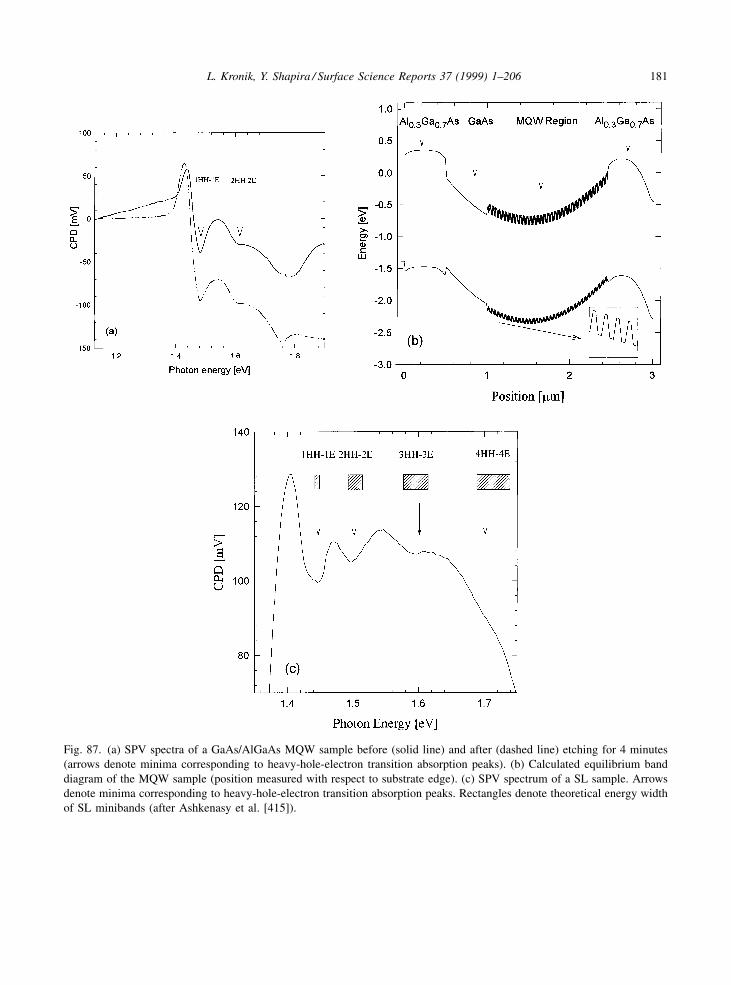
Fig. 87. (a) SPV spectra of a GaAs/AlGaAs MQW sample before (solid line) and after (dashed line) etching for 4 minutes
(arrows denote minima corresponding to heavy-hole-electron transition absorption peaks). (b) Calculated equilibrium band
diagram of the MQW sample (position measured with respect to substrate edge). (c) SPV spectrum of a SL sample. Arrows
denote minima corresponding to heavy-hole-electron transition absorption peaks. Rectangles denote theoretical energy width
of SL minibands (after Ashkenasy et al. [415]).
L. Kronik, Y. Shapira / Surface Science Reports 37 (1999) 1±206 181

structure [777]. In this structure, an InAs wetting layer (WL), which forms a quantum well, is depositedon a GaAs layer. The strong lattice mismatch between the two semiconductors induces the formation ofInAs dots. These dots are then self-organized during ten cycles (in this case) of alternate short-periodGaAs/InAs depositions. This active region of the structure is `inserted' between thin GaAs layers,themselves `inserted' between two GaAs/AlGaAs SLs and AlGaAs cladding layer and sandwiched in aGaAs p±n junction. Both the as-measured SPV spectrum and its normalized derivative for this structure(at 103 K) are shown in Fig. 88 [777]. With the aid of the derivative spectrum, three QD-relatedtransitions and two WL-related transitions are extracted.
Ashkenasy et al. have studied a single quantum well graded-index-of-refraction separate-con®nement heterostructure laser [778]. The studied structure consisted of a single pseudomorphicInGaAs quantum well, `inserted' between two thin GaAs layers and two graded AlGaAs layers andsandwiched in an AlGaAs p±n junction. In this case, four peaks associated with the four `symmetry-allowed' heavy-hole-electron transitions, as well as a ®fth peak due to combination of several`symmetry-forbidden' transitions were observed at room temperature. In this study, numericalsimulations have shown that the energy of the 1HH-1E transition is mostly affected by the mole fractionof the InGaAs layer, whereas the energy of the 2HH-2E transition is primarily sensitive to themagnitude of the electric ®eld in the quantum well, due to the quantum con®ned Stark effect. Thus,these two important parameters could be extracted from the experiment. Using the simulation, thedependence of the energy of the 1HH-1E transition on the electric ®eld was calculated. Speci®cally, its
Fig. 88. SPV spectrum (a) and normalized SPV derivative spectrum (b) of an InAs/GaAs quantum dot structure. The solid line
is a lineshape ®t (after Aigoui et al. [777]).
182 L. Kronik, Y. Shapira / Surface Science Reports 37 (1999) 1±206
value for a small electric ®eld (such as that present during the forward bias required for lasing) wasfound. This enabled a contactless estimate of lasing wavelength, based on layer properties, prior todevice processing. In light of the above discussion, SPS seems to be emerging as a promising tool forthe characterization of quantum structures.
Having described the main developments and achievements of SPS studies of quantum structures, weconclude this section by considering some aspects of SPV generation and spectrum interpretation inquantum structures in more detail. While the absorption features of the quantum structures wereexamined at some length in the above examples, the charge separation mechanism ± required forgetting a SPV signal - was not considered so far. In the discussion of Fig. 87, we assumed that thegenerated electrons and holes are separated by the electric ®eld just like in a non-quantum structure.However, this clearly requires that the excess carriers escape from the quantum well. Severaltemperature-resolved quantum well SPS studies revealed a decrease of the signal with decreasingtemperature [423,771,772,776], whereas the simple photovoltaic effect is expected to increase withdecreasing temperature (see Section 2.2.2). This indicates that carriers escape from the well by meansof thermal excitation, which is insuf®cient at low temperatures. However, as the obtained temperaturedependence is usually non-exponential [771,772], it is clear that other mechanisms, especially ®eld-induced tunneling from the quantum well, also assist in generating the SPV signal.
As long as the cause of the SPV is the separation of charge carriers by the electric ®eld in a SCR, thesign of the SPV signal will re¯ect the direction of this electric ®eld and not the layer type, regardless ofthe exact escape mechanism [415,771]. As in non-quantized structures, it is necessary to consider otherSPV-generating mechanisms to which this sign interpretation scheme does not apply. First, ininterpreting any decrease in the absolute value of the SPV signal, an absorption-induced decrease ofphotovoltaic effects at a layer beneath the light absorbing one must be considered. For example, thequantum-transition-related minima in Fig. 87(a) could partially be due to modulation of the lightintensity arriving at the GaAs layer by the MQW region. However, in this spectrum, recorded understeady-state conditions, the change of sign in the total SPV indicates that at least part of the signal isdue to photovoltaic activity in the MQW region itself. Second, charge separation due to preferentialtrapping of charges must also be considered. For example, Cameron±Miller et al. noticed that theplacement of a GaAs quantum well at the surface of an AlGaAs layer resulted in a photo-inducedincrease in surface band-bending because photo-excited electrons were preferentially trapped in thesurface quantum well [779]. In addition, Karpovich et al. measured a non-negligible SPV signal relatedto InGaAs quantum wells embedded in the quasi-neutral region of a GaAs layer [770,774]. In this case,the only electric ®elds are due to the InGaAs/GaAs heterojunction and must be symmetric with respectto the quantum well. The observation of a SPV in this case must therefore indicate a preferential escapeof one type of carriers from the well, resulting in an effective charge separation.
5.5.3. Construction of band diagrams
The construction of interface band-diagrams is a relatively new application of SPV measurements. A®rst, signi®cant step in this direction was taken by Goldstein et al. [759,760], who performed `depth-pro®led' SPV analyses by measuring solar cell structures after repeated sputtering steps. As anexample, we consider the SPV pro®le of an a-Si:H p±i±n solar cell, shown in Fig. 89 [760]. The SPVpro®le clearly resolves the different layers in the studied structure. Moreover, it elegantly reveals theeffects of prolonged illumination (`light soaking') on the device properties: after illumination, the SCRwidth at the p�±i junction decreases (due to an increase in the effective doping at the i region),
L. Kronik, Y. Shapira / Surface Science Reports 37 (1999) 1±206 183
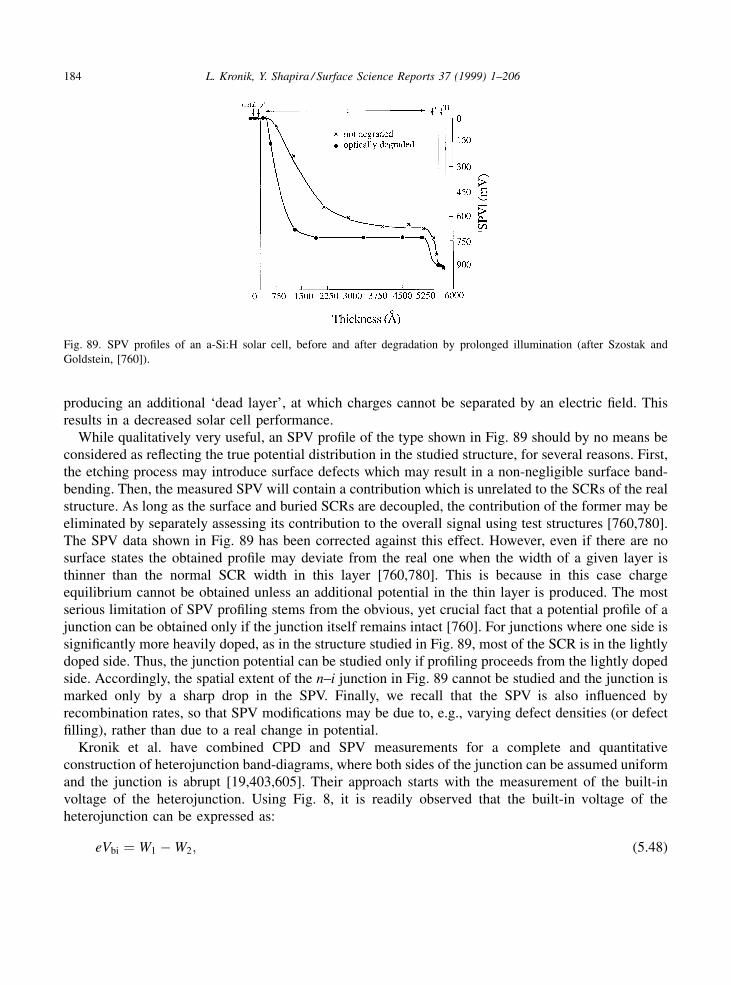
producing an additional `dead layer', at which charges cannot be separated by an electric ®eld. Thisresults in a decreased solar cell performance.
While qualitatively very useful, an SPV pro®le of the type shown in Fig. 89 should by no means beconsidered as re¯ecting the true potential distribution in the studied structure, for several reasons. First,the etching process may introduce surface defects which may result in a non-negligible surface band-bending. Then, the measured SPV will contain a contribution which is unrelated to the SCRs of the realstructure. As long as the surface and buried SCRs are decoupled, the contribution of the former may beeliminated by separately assessing its contribution to the overall signal using test structures [760,780].The SPV data shown in Fig. 89 has been corrected against this effect. However, even if there are nosurface states the obtained pro®le may deviate from the real one when the width of a given layer isthinner than the normal SCR width in this layer [760,780]. This is because in this case chargeequilibrium cannot be obtained unless an additional potential in the thin layer is produced. The mostserious limitation of SPV pro®ling stems from the obvious, yet crucial fact that a potential pro®le of ajunction can be obtained only if the junction itself remains intact [760]. For junctions where one side issigni®cantly more heavily doped, as in the structure studied in Fig. 89, most of the SCR is in the lightlydoped side. Thus, the junction potential can be studied only if pro®ling proceeds from the lightly dopedside. Accordingly, the spatial extent of the n±i junction in Fig. 89 cannot be studied and the junction ismarked only by a sharp drop in the SPV. Finally, we recall that the SPV is also in¯uenced byrecombination rates, so that SPV modi®cations may be due to, e.g., varying defect densities (or defect®lling), rather than due to a real change in potential.
Kronik et al. have combined CPD and SPV measurements for a complete and quantitativeconstruction of heterojunction band-diagrams, where both sides of the junction can be assumed uniformand the junction is abrupt [19,403,605]. Their approach starts with the measurement of the built-involtage of the heterojunction. Using Fig. 8, it is readily observed that the built-in voltage of theheterojunction can be expressed as:
eVbi � W1 ÿW2; (5.48)
Fig. 89. SPV pro®les of an a-Si:H solar cell, before and after degradation by prolonged illumination (after Szostak and
Goldstein, [760]).
184 L. Kronik, Y. Shapira / Surface Science Reports 37 (1999) 1±206
where W1 and W2 are the ideal work functions of the two sides of the heterojunction. In other words,W1 and W2 correspond to the distance between the Fermi level and the local vacuum level in the quasi-neutral region on each side of the heterojunction. In the case of ideal surfaces (i.e, containing no surfaceband-bending and surface dipole), W1 ÿW2 can be measured by subtracting the CPD measured at thefree surface of the complete heterojunction from the CPD measured at the free surface of the substrate(prior to semiconductor deposition). In practice, the measured CPD difference will be given by� CPD � W 01 ÿW 02, where W 01 and W 02 are the real (non-ideal) surface work functions of the substrateand overlayer. Using Fig. 4 and Eq. (2.36) for relating the ideal and real surface work-functions,Eq. (5.48) is recast in the form:
eVbi � W1 ÿW2 � �W 01 ÿ eVs1 ���s1� ÿ �W 02 ÿ eVs2 ���s2�� �CPDÿ �eV0
s1 ÿ eV0s2� � ���s1 ÿ��s2�: (5.49)
Eq. (5.49) shows that the built-in voltage in a real case is still related to �CPD, but must be correctedby the difference in surface band-bending and surface dipole of the two free surfaces. Once Vbi isdetermined (and assuming that the bulk properties are known), the band offsets can be determined usingEqs. (2.43) and (2.46).
Experimentally, �CPD can be easily determined from overlayer-thickness-dependent CPDmeasurements, as shown in Fig. 86. When the overlayer is thick enough to contain a quasi-neutralregion, the CPD reading saturates and the true �CPD is obtained. V0
s1 and V0s2 can be determined by
photosaturation, or any of the techniques described in Section 5.2.2. Then, if the surface and interfacedipoles are estimated (using chemical considerations [605] and/or measurements of the type discussedin Section 5.2.3), the built-in voltage and the heterojunction band offsets can be found.
The above outlined approach seems to be of particular advantage for junctions comprising poly-crystalline or amorphous materials, or for heterojunctions which are not prepared using conventionalUHV fabrication tools. This is because in such junctions many other band-offset measurementtechniques tend to fail, or produce inconclusive data. For establishing its validity, the SPV/CPD-basedapproach was ®rst demonstrated on the In2O3/InP heterojunction, where its results could be easilycon®rmed using I±V analysis due to the degenerately high doping of the In2O3 side [19]. It was thenapplied to the polycrystalline CdS/CIGS heterojunction, manufactured using wet chemical methods,where the band offset values were under considerable debate [605]. Moreover, the measured CPDversus overlayer thickness curve, and hence the extracted band lineup, were found to be independent ofsample annealing (within experimental error) [403].
Complete construction of the equilibrium band-diagram can be obtained by further considering theCPD and super-bandgap SPV evolution shown in Fig. 86. The overlayer thickness at which the CPDand SPV saturate is indicative of the overlayer width at which the surface and interface SCRs decouple,i.e., of the minimal overlayer thickness required to completely sustain the interface SCR. Therefore, anestimate of the SCR width at the overlayer is obtained. Then, the interface charge density (which is theonly remaining independent junction parameter) can be found by ®tting the CPD evolution to producethe measured SCR width in the overlayer [19,605]. Other parameters, e.g., the built-in voltage on eitherside of the junction and the total SCR width, can then be obtained from a solution of the Poissonequation pertaining to the heterojunction, which is based on the measured parameters.
Clearly, the weak point of the above outlined approach is that surface and interface dipoles are notmeasured directly, and therefore limit the experimental accuracy which can practically be obtained to� �100 meV. Leibovitch et al. suggested a different approach for band offset determination, which
L. Kronik, Y. Shapira / Surface Science Reports 37 (1999) 1±206 185

relies solely on SPS measurements and is therefore inherently immune to dipole-induced errors [21].The principle of this approach is shown in Fig. 90, which features the numerically simulated andexperimentally measured SPV spectra of the nÿ-InP/n-In0:53Ga0:47As structure, for various InPoverlayer thicknesses. At large InP overlayers, both simulated and experimental SPV spectra featuretwo distinct `knees' at the InGaAs and InP bandgaps (0.75 and 1.34 eV, respectively), as expected.However, at small overlayer thicknesses, the InP-related `knee' is absent. Additional simulationsshowed that the critical thickness at which the InP-related feature appears, wc, is very strongly
Fig. 90. (a) Numerical simulation of SPV spectra of the nÿ-InP/n-In0:53Ga0:47As structure for various InP overlayer
thicknesses (curve for 200 nm is shifted up by 20 mV for clarity). Inset: magnitude of the spectral `knee' at 1.35 eV vs. InP
overlayer thickness for �Ec � 275 meV and �Ec � 225 meV. (b) Experimental SPV spectra of the same structure for various
overlayer thicknesses (after Leibovitch et al. [21]).
186 L. Kronik, Y. Shapira / Surface Science Reports 37 (1999) 1±206

dependent on the band offsets used. For example, the inset of Fig. 90(a) shows that a change of 50 meVin �Ec changes wc by 25 nm, which is a considerable thickness.
The behavior of the SPV spectra may be explained physically as follows: For small InP overlayerthicknesses, the density of excess carriers generated in the InP layer is negligible with respect to theexcess carrier density injected from the InGaAs side due to the (forward) photo-bias. Therefore, nodiscernible SPV feature is recorded at the onset of absorption in the InP layer. At large overlayerthicknesses, this is no longer true and the InP-related feature can be identi®ed. The strong dependenceof wc on the band offsets is obtained because �Ev determines the barrier height holes must overcomefor crossing into the InP side.
Additional simulations (not shown) have con®rmed that wc changes very little with reasonabledeviations in various bulk sample parameters (e.g., absorption coef®cient, carrier lifetime, etc). Thedominance of the band offsets in determining wc is the key for the determination of the former, as theirvalue can be ®tted to correspond to the experimentally obtained critical thickness. In this case, �Ec wasfound to be 275 meV, in agreement with literature values. Moreover, the strong dependence of wc on�Ec resulted in a relatively small measurement error (only �30 meV), which is considerably superiorto that obtained with the method illustrated in Fig. 86. On the other hand, whereas the latter is inprinciple, applicable to any heterojunction interface, the method illustrated in Fig. 90 is not expected tobe universal in nature.
Moons et al. have recently used a different type of SPV-based construction of the band diagrams, inthe context of a study of porphyrin/ITO structures [413], already mentioned in Section 5.5.1. In thisstudy, the porphyrin overlayer was fully depleted, so that its front and back SCR were not separated bya quasi-neutral region. Because the SPV due to the front SCR was found to dominate (seeSection 5.5.1), the contribution of the back (porphyrin/ITO) SCR was assumed to be negligible. Thus,photosaturation measurements at the porphyrin bandgap were assumed to yield the band-bending at thefront SCR and additional illumination at the ITO bandgap was assumed to yield the band-bending at theITO part of the porphyrin/ITO interface. Interface charge densities could then be extracted from simplecharge balance considerations.
Just like the approach of Leibovitch et al., the analysis of Moons et al. does not utilize CPDmeasurements and is therefore, also immune to dipole-related errors. Moreover, thickness-resolvedmeasurements are not used so that all analysis can be conducted on the ®nished structure. The problemwith the analysis of Moons et al., however, is that it neglects the coupling of the different SCRs in thestructure. Even if absorption at the porphyrin part of the back SCR per se truly results in a negligibleSPV, this SCR would still affect the other saturation measurements because excess carriers excited inthe front porphyrin SCR and/or in the ITO would be injected into the back porphyrin SCR. Suchcoupling was indeed observed in the InP/InGaAs SPV simulations of Fig. 90(a). For, e.g., an InPoverlayer thickness of 200 nm, the equilibrium band-bending in the InGaAs layer was only 50 mV, butthe InGaAs-related SPV signal was well over 200 mV. As it is clearly impossible that the SPV wouldexceed the equilibrium band-bending by over 150 mV, charge carriers were evidently injected into theInP side of the heterojunction, as explained above. This effect makes it impossible to use (or indeedobtain) photosaturation for selective determination of the band-bending in one part of a heterojunctionor in one part of coupled SCRs.
The approaches outlined above indicate the potential of SPV tools for the extraction of quantitativeinformation on various aspects of interface band-diagrams. As this particular sub-®eld of SPV isrelatively young, only a handful of experimental examples may be found in the literature. However, we
L. Kronik, Y. Shapira / Surface Science Reports 37 (1999) 1±206 187
believe that much more work can be done in this direction. Speci®cally, various analyses of themeasurements of SPV data as a function of overlayer thickness (as in Figs. 86, 89 and 90), seem to beof particular promise.
6. Concluding remarks
In this review article, we have endeavored to provide an in-depth examination of all aspects of SPVtechniques, including theory, experiment, and applications. Speci®cally, we have attempted to show thatSPV-based analyses constitute a highly evolved tool for the characterization of semiconductor materialsand structures, with a unique combination of many advantages.
SPV measurements re¯ect both optical properties and transport properties, because the photo-voltaic effect is based on photo-generation of excess carriers which is followed by their spatialseparation. The measurements are highly sensitive because even a very small optical absorption, e.g., indefect states, may result in a signi®cant photovoltaic signal. Moreover, they can be used to probe anyphotovoltage developed in the sample under study, be it at its surface, at its bulk, or at any buriedinterface.
The unique sensitivity to many electrical and optical properties of different regions in the sample ismanifested by the wide range of characterization capabilities afforded by SPV analyses. The latter canprovide detailed, quantitative information on bulk properties (e.g., bandgap and type, carrier diffusionlength and lifetime), on surface and interface band-diagrams, and on energy levels in quantumstructures. A particular strength is that a complete analysis of surface and bulk defect state distributionsand properties is afforded. A different testament to the versatility of SPV measurements is that theyhave been shown to emulate absorption measurements (Sections 4.1 and 5.5), capacitance measure-ments (Section 5.2), and even photoconductivity measurements (Section 5.4.2), depending on sampleproperties and experimental conditions.
Experimentally, SPV measurements feature many advantages: First and foremost, they arecontactless and non-destructive. In addition, they can be performed both in-situ and ex-situ, at anyreasonable temperature (from several K to many hundreds of K), at any ambient (be it air or othergases, vacuum, or even a liquid), and at any lateral resolution, down to the atomic scale. Traditionally,these characteristics have made SPV analyses attractive for basic studies of the effects of variousphysical and chemical processes on semiconductor properties in general and on the surface electronicstructure in particular. In recent years, the same properties are being increasingly used for qualitycontrol and process monitoring of both materials and structures. This trend is especially apparent in theSi industry, where several companies now offer different kinds of SPV-based inspection stations,discussed in Section 5.
The sensitivity of SPV measurements to a plethora of physical phenomena is a double-edged swordbecause it requires very careful experiment design and data interpretation for the (qualitative orquantitative) extraction of speci®c properties. Signi®cant strides have been made in this direction andmuch of this text has been devoted to presenting tools to that end.
Throughout our discussion, we have emphasized not only the advantages and achievements ofany given approach, but also its limitations and shortcomings. We therefore believe that ourpresentation could serve as a roadmap for both current capabilities and further development of thetechnique.
188 L. Kronik, Y. Shapira / Surface Science Reports 37 (1999) 1±206
Acknowledgements
This review has bene®ted from many illuminating discussions with Dr. Mark Leibovitch (Elta, Israel)and from critical reading of portions of the manuscript by Ilan Shalish, Gaby Segal, and NuritAshkenasy (Tel-Aviv University, Israel), and Dr. Ellen Moons (Cambridge University, England).
We wish to thank the following individuals for sharing their insight and data on speci®c subjects inthe review (in order of appearance in the text): Dr. Guy Cohen (IBM Watson Research Center, USA) -atomic force microscopy; Dr. Gady Haase (Weizmann Institute of Science, Israel) - scanning tunnelingmicroscopy; Prof. Jacek Lagowski (Semiconductor Diagnostics, USA) - diffusion length measure-ments; Prof. Isaac Balberg (Hebrew University, Israel) - SPV of amorphous silicon; Dr. John Lowell(Applied Materials, USA) and Dr. Krzystof Nauka (Hewlett Packard, USA) - photosaturationmeasurements of Si wafers; Dr. Emil Kamieniecki (QC Solutions, USA) - surface charge Pro®ling; Mr.Charles Kohn and Mr. Sergei Liberman (SemiTest, USA) - surface charge analysis; Prof. David Cahen(Weizmann Institute of Science, Israel) - surface band-bending and dipole.
Many thanks are due to Ms. Dina Levine and Mr. Oleg Tilishevsky for their expert computer help ingraphics and text, respectively.
LK is deeply indebted to his family for bearing with him during the writing of this text. He alsowishes to add a special, personal thank you to Dr. David Rosenfeld and to Dr. Jasmin Oz.
YS is indebted to Dinah and Henry Krongold for their generous support in establishing the KrongoldChair of Microelectronics at Tel Aviv University.
References
[1] W.H. Brattain, Phys. Rev. 72 (1947) 345.
[2] W.H. Brattain, J. Bardeen, Bell System Tech. J. 32 (1953) 1.
[3] C.G.B. Garrett, W.H. Brattain, Phys. Rev. 99 (1955) 376.
[4] E.O. Johnson, J. Appl. Phys. 28 (1957) 1349.
[5] A.M. Goodman, J. Appl. Phys. 32 (1961) 2550.
[6] H.C. Gatos, J. Lagowski, J. Vac. Sci. Technol. 10 (1973) 130.
[7] L.J. Brillson, Surf. Sci. Rep. 2 (1982) 123, and references therein.
[8] G. Heiland, W. MoÈnch, Surf. Sci. 37 (1973) 30.
[9] H. LuÈth, Appl. Phys. 8 (1975) 1.
[10] H. LuÈth, G. Heiland, Il Nuovo Cimento 39 (1977) 748.
[11] W. MoÈnch, in: R. Vanselow, R. Howe (Eds), Chemistry and Physics of Solid Surfaces, V, vol. 35 of the Springer Series in
Chemical Physics, Springer, Berlin, 1984.
[12] J. Lagowski, P. Edelman, M. Dexter, W. Henley, Semicond. Sci. Technol. 7 (1992) A185.
[13] R.J. Hamers, K. Markert, Phys. Rev. Lett. 64 (1990) 1051; J. Vac. Sci. Technol. A8 (1990) 3524 .
[14] Y. Kuk, R.S. Becker, P.J. Silverman, G.P. Kochanski, Phys. Rev. Lett. 65 (1990) 456; J. Vac. Sci. Technol. B9 (1991) 545.
[15] J.M.R. Weaver, H.K. Wickramasinghe, J. Vac. Sci. Technol. B9 (1991) 1562.
[16] M. Alonso, R. Cimino, K. Horn, Phys. Rev. Lett. 64 (1990) 1947.
[17] M.H. Hecht, Phys. Rev. B41 (1990) 7918; J. Vac. Sci. Technol. B8 (1990) 1018.
[18] C.M. Aldao, G.D. Waddill, P.J. Benning, C. Capasso, J.H. Weaver, Phys. Rev. B41 (1990) 6092.
[19] L. Kronik, M. Leibovitch, E. Fefer, V. Korobov, Y. Shapira, J. Electron. Mater. 24 (1995) 893; M. Leibovitch, L. Kronik,
E. Fefer, V. Korobov, Y. Shapira, Appl. Phys. Lett. 66 (1995) 457.
[20] M. Leibovitch, L. Kronik, E. Fefer, L. Burstein, V. Korobov, Y. Shapira, J. Appl. Phys. 79 (1996) 8549.
[21] M. Leibovitch, L. Kronik, B. Mishori, Y. Shapira, C.M. Hanson, A.R. Clawson, Appl. Phys. Lett. 69 (1996) 2587.
[22] A. Many, Y. Goldstein, N.B. Grover, Semiconductor Surfaces, 2nd ed., North-Holland, Amsterdam, 1971.
L. Kronik, Y. Shapira / Surface Science Reports 37 (1999) 1±206 189
[23] W. MoÈnch, Semiconductor Surfaces and Interfaces, Springer, Berlin, 1993.
[24] H. LuÈth, Surfaces and Interfaces of Solids, 2nd ed., Springer, Berlin, 1993.
[25] S.M. Sze, Physics of Semiconductor Devices, 2nd ed., Wiley, New York, 1981.
[26] M. Shur, Physics of Semiconductor Devices, Prentice-Hall, New Jersey, 1990.
[27] S. Selberherr, Analysis and Simulation of Semiconductor Devices, Springer, Vienna, 1984.
[28] S.G. Davison, M. Steslicka, Basic Theory of Surface States, Clarendon Press, Oxford, 1992.
[29] W. Shockley, W.T. Read, Jr., Phys. Rev. 87 (1952) 835; R.N. Hall, Phys. Rev. 87 (1952) 387.
[30] D.K. Schroder, Semiconductor Material and Device Characterization, Wiley, New York, 1990.
[31] R.F. Pierret, in: R.F. Pierret, G.W. Neudeck (Eds.), Advanced Semiconductor Fundamentals, Modular Series on Solid
State Devices, Vol. VI, Addison-Wesley, Reading, 1987.
[32] J. Bonnet, L. Soonckindt, L. Lassabatere, Thin Solid Films 91 (1982) 283.
[33] R.B. Darling, Phys. Rev. B43 (1991) 4071.
[34] R.H. Kingston, S.F. Neustadter, J. Appl. Phys. 26 (1955) 718.
[35] J.R. Maltby, C.E. Reed, C.G. Scott, Surf. Sci. 51 (1975) 89.
[36] W. Jaegermann, Mod. Aspects Electrochem. 30 (1996) 1.
[37] W. Ranke, Y.R. Xing, Phys. Rev. B31 (1985) 2246; H. J. Kuhr, W. Ranke, Solid State Commun. 61 (1987) 285.
[38] R. Nicolini, L. Vanzetti, G. Mula, G. Bratina, L. Sorba, A. Franciosi, M. Peressi, S. Baroni, R. Resta, A. Baldereschi, J.E.
Angelo, W.W. Gerberich, Phys. Rev. Lett. 72 (1994) 294.
[39] J. Tersoff, Phys. Rev. B30 (1984) 4874; J. Tersoff, Phys. Rev. Lett. 56 (1986) 2755.
[40] N.E. Christensen, Phys. Rev. 37 (1988) 4528.
[41] W.R.L. Lambrecht, B. Segall, O.K. Anderson, Phys. Rev. 41 (1990) 2813.
[42] A.H. Marshak, IEEE Trans. Elec. Dev. 36 (1989) 1764.
[43] A.M. Cowley, S.M. Sze, J. Appl. Phys. 36 (1965) 3212.
[44] B.L. Sharma (Ed.), Metal-Semiconductor Schottky Barrier Junctions and Their Applications, Plenum Press, New York,
1984.
[45] R.L. Anderson, Solid State Electron. 5 (1962) 341.
[46] L.J. van Ruyven, Phys. Stat. Sol. 5 (1964) K109.
[47] See, for example, F. Capasso, G. Margaritondo (Eds), Heterojunction Band Discontinuities, North-Holland, Amsterdam,
1987, and references therein.
[48] A. Franciosi, C.G. Van de Walle, Surf. Sci. Rep. 25 (1996) 1, and references therein.
[49] T. dell'Orto, J. Almeida, C. Coluzza, A. Baldereschi, G. Margaritondo, M. Cantile, S. Yildirim, L. Sorba, A. Franciosi,
Appl. Phys. Lett. 64 (1994) 2111; M. Marsi, R. Houdre, A. Rudra, M. Ilegems, F. Gozzo, C. Coluzza, G. Margaritondo,
Phys. Rev. B47 (1993) 6455.
[50] E. Moons, M. Bruening, L. Burstein, J. Libman, A. Shanzer, D. Cahen, Jpn. J. Appl. Phys. 32 (suppl. 32-3) (1992) 730.
[51] M. Bruening, E. Moons, D. Yaron-Marcovich, D. Cahen, J. Libman, A. Shanzer, J. Am. Chem. Soc. 116 (1994) 2972.
[52] M. Bruening, E. Moons, D. Cahen, A. Shanzer, J. Phys. Chem. 99 (1995) 8368.
[53] S. Bastide, R. Butruille, D. Cahen, A. Dutta, J. Libman, A. Shanzer, L. Sun, A. Villan, J. Phys. Chem. B101 (1997) 2678.
[54] M. Bruening, R. Cohen, J.F. Guillemoles, T. Moav, J. Libman, A. Shanzer, D. Cahen, J. Am. Chem. Soc. 119 (1997) 5720.
[55] R. Cohen, S. Bastide, D. Cahen, J. Libman, A. Shanzer, Y. Rosenwaks, Adv. Mater. 9 (1997) 746.
[56] R. Cohen, S. Bastide, D. Cahen, J. Libman, A. Shanzer, Y. Rosenwaks, Opt. Mater. 9 (1998) 394.
[57] R. Cohen, N. Zenou, D. Cahen, S. Yitzchaik, Chem. Phys. Lett. 279 (1997) 270.
[58] I.H. Campbell, S. Rubin, T.A. Zawodinski, J.D. Kress, R.L. Martin, D.L. Smith, N.N. Barashkov, J.P. Ferraris, Phys. Rev.
B54 (1996) 14321; I.M. Dharmadasa, G.G. Roberts, M.C. Petty, Electron. Lett. 16 (1980) 201.
[59] K.K. Ng, Complete Guide to Semiconductor Devices, McGraw-Hill, New York, 1995.
[60] See, for example, Yu.Ya. Gurevich, Yu.V. Pleskov, Z.A. Rotenberg, Photoelectrochemistry, Consultant Bureau, New
York, 1980.
[61] H. Dember, Physik. Zeitschr. 32 (1931) 554; H. Dember, Physik. Zeitschr. 32 (1931) 856.
[62] L.J. Richter, R.R. Cavanagh, Progr. Surf. Sci. 39 (1992) 155.
[63] Y.K. Hsieh, H.C. Card, J. Appl. Phys. 65 (1989) 2409.
[64] A.V. Sachenko, Sov. Phys. Semicond. 12 (1978) 1120.
[65] D.R. Frankl, Surf. Sci. 3 (1965) 101.
[66] E.O. Johnson, Phys. Rev. 111 (1958) 153.
190 L. Kronik, Y. Shapira / Surface Science Reports 37 (1999) 1±206
[67] D.R. Frankl, E.A. Ulmer, Surf. Sci. 6 (1966) 115.
[68] W.H. Brattain, C.G.B. Garrett, Bell Syst. Tech. J. 35 (1956) 1019; C.G.B. Garrett, W.H. Brattain, Bell Syst. Tech. J. 35
(1956) 1041.
[69] V.M. Buimistrov, A.P. Gorban, V.G. Litovchenko, Surf. Sci. 3 (1965) 445.
[70] G. Brouwer, Philips Res. Repts. 18 (1963) 432.
[71] S.S. De, A.K. Ghosh, T.K. Pattanyak, J. Can. Phys. 69 (1991) 616; 69 (1991) 732.
[72] T.S. Moss, J. Elect. and Control, 1 (1955) 126.
[73] C.-L. Chiang, S. Wagner, IEEE Trans. Elect. Dev. ED-32 (1985) 1722.
[74] D.L. Lile, Surf. Sci. 34 (1973) 337.
[75] V.A. Zuev, V.G. Litovchenko, Phys. Stat. Sol. 16 (1966) 751.
[76] X. Zhang, J. Song, J. Appl. Phys. 70 (1991) 4632.
[77] S.C. Choo, L.S. Tan, K.B. Quek, Sol. State Electr. 35 (1992) 269.
[78] S.C. Choo, L.S. Tan, H.H. See, Sol. State Electr. 36 (1993) 989.
[79] S.R. Dhariwal, B.M. Deoraj, Semicond. Sci. Technol. 8 (1993) 372.
[80] S.C. Choo, Sol. State Electr. 38 (1995) 2085.
[81] C.R. Crowell, S.M. Sze, Sol. State Electr. 9 (1966) 1035.
[82] M.A. Green, J. Shewchun, Sol. State Electr. 16 (1973) 1141.
[83] P. Panayotatos, H.C. Card, Sol. State Electr. 23 (1980) 41.
[84] E.L. Heasell, Sol. State Electr. 24 (1981) 889.
[85] H.J. Pauwels, P. De Vischere, P. Reussens, Sol. State Electr. 21 (1978) 775.
[86] P. De Visschere, Sol. State Electr. 25 (1982) 955.
[87] S.-L. Jang, Sol. State Electr. 34 (1991) 373.
[88] O.V. Konstantinov, B.V. Tsarenkov, Sov. Phys. Semicond. 24 (1990) 1319.
[89] Q. Liu, H.E. Ruda, G.M. Chen, M. Simard-Normandin, J. Appl. Phys. 79 (1996) 7790.
[90] J.P. McKelvey, Solid State and Semiconductor Physics, Harper and Row, New York, 1966.
[91] R.S. Nakhmanson, Solid State Electron. 18 (1975) 617.
[92] R.S. Nakhmanson, Int. J. Electron. 59 (1985) 685.
[93] C. Munakata, S. Nishimatsu, Jpn. J. Appl. Phys. 22 (1983) 1893.
[94] C. Munakata, S. Nishimatsu, N. Honma, K. Yagi, Jpn. J. Appl. Phys. 23 (1984) 1451.
[95] C. Munakata, S. Nishimatsu, Jpn. J. Appl. Phys. 25 (1986) 807.
[96] C. Munakata, Jpn. J. Appl. Phys. 27 (1988) 759.
[97] E. Kamieniecki, J. Appl. Phys. 54 (1983) 6481; E. Kamieniecki, J. Vac. Sci. Technol. 20 (1982) 811.
[98] C.M. Wolfe, N. Holonyak, G.E. Stillman, Physical Properties of Semiconductors, Prentice Hall, New Jersey, 1989.
[99] C.L. Balestra, J. Lagowski, H.C. Gatos, Surf. Sci. 26 (1971) 317.
[100] E.V. Ostroumova, Sov. Phys. Semicond. 3 (1970) 926.
[101] F. Steinrisser, R.E. Hetrick, Surf. Sci. 28 (1971) 607.
[102] J.H. Dinan, L.K. Galbraith, T.E. Fischer, Surf. Sci. 26 (1971) 587.
[103] J. Lagowski, C.L. Balestra, H.C. Gatos, Surf. Sci. 27 (1971) 547.
[104] L. Szaro, Appl. Phys. A29 (1982) 201.
[105] K.Y. Tong, Y.W. Lam, J. Phys. D: Appl. Phys. 9 (1976) L9.
[106] G. Lucovsky, Solid State Commun. 3 (1965) 299.
[107] G. Grimmeiss, L.-AÊ . Ledebo, J. Phys. C: Solid State Phys. 8 (1975) 2615.
[108] A.L. Musatov, S.V. Geizer, Sov. Phys. Solid State 33 (1991) 69.
[109] J. Lagowski, H.C. Gatos, Surf. Sci. 38 (1973) 252.
[110] J. Lagowski, C.L. Balestra, H.C. Gatos, Surf. Sci. 29 (1972) 203.
[111] K.G. Germanova, L.L. Konstantinov, V.L. Strashilov, Surf. Sci. 128 (1983) 447.
[112] L. Szaro, Surf. Sci. 137 (1984) 311.
[113] I.A. Davydov, L.P. Strakhov, S.L. Tselishchev, Sov. Phys. Semicond. 26 (1992) 89.
[114] L. Szaro, Phys. Stat. Sol. (a)113 (1989) 97.
[115] L. Szaro, Semicond. Sci. Technol. 6 (1991) 875.
[116] M. Leibovitch, L. Kronik, E. Fefer, Y. Shapira, Phys. Rev. B50 (1994) 1739.
[117] A.N. Ishaque, J.W. Howard, M. Becker, R.C. Block, J. Appl. Phys. 69 (1991) 307.
L. Kronik, Y. Shapira / Surface Science Reports 37 (1999) 1±206 191

[118] Q. Liu, C. Chen, H. Ruda, J. Appl. Phys. 74 (1993) 7493.
[119] R.M. Esposito, J.J. Loferski, H. Flicker, J. Appl. Phys. 38 (1967) 825.
[120] G. Nadzhakov, S. Balabanov, Sov. Phys. Solid State, 7 (1965) 957.
[121] I.F. Patai, M.A. Pomerantz, J. Franklin Inst. 252 (1951) 239.
[122] W. Thomson (Lord Kelvin), Phil. Mag. 46 (1898) 82.
[123] W.A. Zisman, Rev. Sci. Instrum. 3 (1932) 367.
[124] J.R. Anderson, A.E. Alexander, Aust. J. Appl. Sci. 3 (1952) 201.
[125] J.R. MacDonald, D.E. Edmonson, Proc. IRE 49 (1961) 453.
[126] J. Bonnet, J.M. Palau, L. Soonckindt, L. Lassabatere, J. Phys. E; Sci. Instrum. 10 (1977) 212.
[127] K.A. MacFadyen, T.A. Holbeche, J. Sci. Instrum. 34 (1957) 101.
[128] R.E. Simon, Phys. Rev. 116 (1959) 613.
[129] H. Palevsky, R.K. Swank, R. Grenchik, Rev. Sci. Instrum. 18 (1947) 298.
[130] J.R. Maltby, C.E. Reed, C.G. Scott, J. Phys. E: Sci. Instrum. 5 (1972) 584.
[131] L.B. Harris, J. Fiasson, J. Phys. E; Sci. Instrum. 17 (1984) 788.
[132] S.-M. Huang, R.T. Atanasoski, R.A. Oriani, J. Electrochem. Soc. 140 (1993) 1065.
[133] W.E. Meyerhof, P.H. Miller, Rev. Sci. Instrum. 17 (1946) 15.
[134] A.A. Frost, Rev. Sci. Instrum. 17 (1946) 266.
[135] H.P. Myers, Proc. Phys. Soc. B66 (1953) 493.
[136] H.G. Yamins, W.A. Zisman, J. Chem. Phys. 1 (1933) 656.
[137] E.F. Porter, J. Am. Chem. Soc. 59 (1937) 1883.
[138] S. Rosenfeld, W.M. Hoskins, Rev. Sci. Instrum. 16 (1945) 343.
[139] J.G. Potter, Phys. Rev. 58 (1940) 623.
[140] A.A. Frost, V.R. Hurka, J. Am. Chem. Soc. 62 (1940) 3336.
[141] J.C.P. Mignolet, Disc. Faraday Soc. 8 (1950) 326.
[142] I.D. Baikie, Rev. Sci. Instrum. 60 (1989) 930.
[143] C. Suresh Kumar, A. Subrahmanyam, J. Majhi, Rev. Sci. Instrum. 67 (1996) 805.
[144] K. Besocke, S. Berger, Rev. Sci. Instrum. 47 (1976) 840.
[145] K. Germanova, Ch. Hardalov, V. Strashilov, B. Goergiev, J. Phys. E: Sci. Instrum. 20 (1987) 273.
[146] Y.L. Yousef, A. Mishriki, S. Aziz, H. Mikhail, J. Sci. Instrum. 42 (1965) 873.
[147] E. Weismann, Ch. Petrescu, D. Tarina, J. Phys. E: Sci. Instrum. 1 (1968) 426.
[148] S.C. Fain, L.V. Corbin, J.M. McDavid, Rev. Sci. Instrum. 47 (1976) 345.
[149] J.C. RivieÁre, Proc. Phys. Soc. B70 (1957) 676.
[150] S. Danyluk, J. Phys. E; Sci. Instrum. 5 (1972) 478.
[151] J. Fiasson, L.B. Harris, J. Phys. E; Sci. Instrum. 10 (1977) 1160.
[152] J.P. Bellier, J. Lecoeur, C. Koehler, Rev. Sci. Instrum. 66 (1995) 5544.
[153] T. Delchar, A. Eberhagen, F.C. Tompkins, J. Sci. Instrum. 40 (1963) 105.
[154] T.K. Bodrova, I.A. Davydov, Yu.V. Protasov, V.T. Seregin, L.P. Strakhov, Inst. Expt. Tech. 29 (1986) 216.
[155] D.P. Woodruff, T.A. Delchar, Modern Techniques of Surface Science, 2nd ed., Cambridge University Press, Cambridge,
1994.
[156] N.A. Surplice, R.J. D'Arcy, J. Phys. E: Sci. Instrum. 3 (1970) 477.
[157] K.B. Johnson, W.N. Hansen, Rev. Sci. Instrum. 66 (1995) 2967.
[158] S. Lundgren, B. Kasemo, Rev. Sci. Instrum. 66 (1995) 3976.
[159] J. Nowotny, M. Sloma, W. Weppner, J. Am. Ceram. Soc. 72 (1989) 564.
[160] P.A. Anderson, Phys. Rev. 88 (1952) 655.
[161] A. Hadjadj, P. Roca i Cabarrocas, B. Equer, Rev. Sci. Instrum. 66 (1995) 5272.
[162] G. Wedler, R. Ruhmann, Appl. Surf. Sci. 14 (1982) 137.
[163] H.H. Kolm, Rev. Sci. Instrum. 27 (1956) 1046.
[164] W. Schaaffs, Z. Angew. Phys. 10 (1958) 424.
[165] E.S. Zanoria, K. Hamall, S. Danyluk, A.L. Zharin, J. Test. Eval. 25 (1997) 233.
[166] T.A. Delchar, G. Ehrlich, J. Chem. Phys. 42 (1965) 2686.
[167] M. Schmidt, M. Nohlen, G. Bermes, M. BoÈhmer, K. Wandelt, Rev. Sci. Instrum. 68 (1997) 3866.
[168] J. HoÈlzl, P. Schrammen, Appl. Phys. 3 (1974) 353.
192 L. Kronik, Y. Shapira / Surface Science Reports 37 (1999) 1±206

[169] T.L. Ashcraft, J. Riney, N. Hackerman, Rev. Sci. Instrum. 34 (1963) 5.
[170] J.C. Mitchinson, R.D. Pringle, W.E.J. Farvis, J. Phys. E: Sci. Instrum. 4 (1970) 525.
[171] P. Freyer, H.-D. Ohlenbusch, J. Sci. Instrum. 44 (1967) 443.
[172] W.N. Hansen, K.B. Johnson, Surf. Sci. 316 (1994) 373.
[173] T. Fort, R.L. Wells, Surf. Sci. 12 (1968) 46.
[174] S. Yee, R.A. Oriani, M. Stratmann, J. Electrochem. Soc. 138 (1991) 55.
[175] I. Baikie, S. Mackenzie, P.J.Z. Estrup, J.A. Meyer, Rev. Sci. Instrum. 62 (1991) 1326.
[176] F. Rossi, Rev. Sci. Instrum. 63 (1992) 4174.
[177] B. Ritty, F. Wachtel, R. Manquenoille, F. Ott, J.B. Donnet, J. Phys. E: Sci. Instrum. 15 (1982) 310.
[178] B.H. Blott, T.J. Lee, J. Phys. E: Sci. Instrum. 2 (1969) 785.
[179] P.P. Craig, V. Radeka, Rev. Sci. Instrum. 41 (1970) 258.
[180] J.H. Parker, R.W. Warren, Rev. Sci. Instrum. 33 (1962) 948.
[181] R.J. D'Arcy, N.A. Surplice, J. Phys. D; Appl. Phys. 3 (1970) 482.
[182] J.S.W. de Boer, H.J. Krusmeyer, N.C. Burhoven Jaspers, Rev. Sci. Instrum. 44 (1973) 1003.
[183] I. Baikie, E. Venderbosch, J.A. Meyer, P.J.Z. Estrup, Rev. Sci. Instrum. 62 (1991) 725.
[184] H.A. Engelhardt, P. Feulner, H. PfnuÈr, D. Menzel, J. Phys. E; Sci. Instrum. 10 (1977) 1133.
[185] J. Bonnet, L. Soonckindt, L. Lassabatere, Vacuum, 34 (1984) 693.
[186] S. Saito, T. Soumura, T. Maeda, J. Vac. Sci. Technol. A2 (1984) 1389.
[187] C. Herring, M.H. Nichols, Rev. Mod. Phys. 21 (1949) 185.
[188] M. Wolff, A.E. Guille, D.J. Bell, J. Phys. E: Sci. Instrum. 2 (1969) 921.
[189] R.E. Collins, O.R. French, Rev. Sci. Instrum. 51 (1980) 547.
[190] H. BaumgaÈrtner, U. Hornung, H.-D. Liess, E. Ederle, Archiv FuÈr Elektrotech. 76 (1993) 265.
[191] S. Sakalauskas, G. Dreyfus, J. Lewiner, J. Phys. E: Sci. Instrum. 8 (1975) 837.
[192] F. Rossi, Rev. Sci. Instrum. 63 (1992) 3744.
[193] L.K. Galbraith, T.E. Fischer, Surf. Sci. 30 (1972) 185.
[194] B. Ritty, F. Wachtel, F. Ott, R. Manquenoille, J.B. Donnet, Rev. Sci. Instrum. 51 (1980) 1421.
[195] K. Germanova, L. Nikolov, Ch. Hardalov, Rev. Sci. Instrum. 60 (1989) 749.
[196] J. Baczynski, Rev. Sci. Instrum. 59 (1988) 2471.
[197] J. M. Palau, J. Bonnet, J. Phys. E: Sci. Instrum. 21 (1988) 674.
[198] R.W. Pasco, P.J. Ficalora, Rev. Sci. Instrum. 51 (1980) 246.
[199] Y. Petit-Clerk, J.D. Carette, Rev. Sci. Instrum. 39 (1968) 933.
[200] J.B. Camp, T.W. Darling, R.E. Brown, J. Appl. Phys. 69 (1991) 7126.
[201] I.D. Baikie, G.H. Bruggink, Proc. MRS Symp. 315 (1993) 423.
[202] R. Butz, H. Wagner, Appl. Phys. 13 (1977) 37.
[203] H. BaumgaÈrtner, H.D. Liess, Rev. Sci. Instrum. 59 (1988) 802.
[204] A. Broniatowski, W. Nabhan, B. Equer, G. de Rosny, Mater. Sci. Forum, 207-209 (1996) 149.
[205] R. MaÈckel, H. BaumgaÈrtner, J. Ren, Rev. Sci. Instrum. 64 (1993) 694.
[206] H.-D. Liess, R. MaÈckel, J. Ren, Surf. Int. Anal., 25 (1997) 855.
[207] H. BaumgaÈrtner, Meas. Sci. Technol. 3 (1992) 237.
[208] W. Nabhan, B. Equer, A. Broniatowski, G.de Rosny, Rev. Sci. Instrum. 68 (1997) 3108.
[209] Bescoke Delta Phi GMBH, Tuchenbleiche 8, D-52428 JuÈlich, Germany.
[210] KP-6000, McAllister Technical Serivces, West 280 Prarie Avenue, Coeur d'Alene, ID 83815, USA.
[211] Uniscan Instruments, Sigma House, Burlow Road, Buxton, Derbyshire, SK179JB, United Kingdom.
[212] S.R. Morrison, J. Phys. Chem. 57 (1953) 860.
[213] C. Munakata, K. Yagi, T. Warabisako, M. Nanba, S. Matsubara, Jpn. J. Appl. Phys. 21 (1982) 624.
[214] J. Schulz, P. WuÈrfel, W. Ruppel, Phys. Stat. Sol. (b)164 (1991) 425.
[215] K. Kinameri, C. Munakata, K. Mayama, J. Phys. E: Sci. Instrum. 21 (1988) 91.
[216] J. HlaÂvka, R. SÏvehla, Rev. Sci. Instrum. 67 (1996) 2588.
[217] A.M. Meshkov, I.A. Akimov, Inst. Expt. Technol. 4 (1964) 674.
[218] J.L. Shohet, K. Nauka, P. Rissman, IEEE Trans. Plasma. Sci. 24 (1996) 75.
[219] V.E. Kozhevin, Sov. Phys. Solid State, 8 (1967) 1979.
[220] C. Munakata, M. Nanba, S. Matsubara, Jpn. J. Appl. Phys. 20 (1981) L137.
L. Kronik, Y. Shapira / Surface Science Reports 37 (1999) 1±206 193
[221] C. Munakata, S. Okazaki, K. Yagi, Jpn. J. Appl. Phys. 21 (1982) L555.
[222] C. Munakata, S. Matsubara, J. Phys. D: Appl. Phys. 16 (1983) 1093.
[223] C. Munakata, N. Honma, H. Hayakawa, Jpn. J. Appl. Phys. 23 (1984) 778.
[224] K. Kinameri, C. Munakata, N. Honma, H. Shimizu, Scan. Microsc., 2 (1988) 1237.
[225] K. Kinameri, C. Munakata, T. Abe, Meas. Sci. Technol. 1 (1990) 621.
[226] H. Shimizu, C. Munakata, N. Honma, S. Aoki, Y. Kosaka, Jpn. J. Appl. Phys. 31 (1992) 1817.
[227] N. Honma, H. Shimizu, C. Munakata, Jpn. J. Appl. Phys. 32 (1993) 3639.
[228] H. Shimizu, N. Honma, C. Munakata, M. Ota, Jpn. J. Appl. Phys. 27 (1988) 1454.
[229] C. Munakata, K. Watanabe, Semicond. Sci. Technol. 6 (1991) 612.
[230] H. Shimizu, C. Munakata, Jpn. J. Appl. Phys. 33 (1994) 3335.
[231] H. Shimizu, C. Munakata, Appl. Phys. Lett. 64 (1994) 3598.
[232] SPV station, Semiconductor Diagnostics, 6604 Harney Road, Tampa, FL 33610, USA.
[233] SPV option for the WT-85 lifetime scanner, Semilab ± Semiconductor Physics Laboratory Rt., 1327 Budapest, UÂ jpest 3,
P.O. Box 18, Hungary.
[234] SCA-2500 surface charge analyzer, SemiTest, 43 Manning Road, Billerica, MA 01821-0812, USA.
[235] SCP-7200 surface charge pro®ler, QC solutions, 150-U New Boston Street, Woburn, MA 01801, USA.
[236] M. Cardona, L. Ley, in: M. Cardona, L. Ley (Eds), Photoemission in Solids I, Topics in Applied Physics, Vol. 28, Springer,
Berlin, 1978.
[237] G. Wlerick, Physica, 20 (1954) 1099.
[238] G.K. Zyrianov, Sov. Phys. Tech. Phys. 3 (1958) 2429.
[239] F. Steinrisser, R. E. Hetrick, Rev. Sci. Instrum. 42 (1971) 304.
[240] M. Henzler, J. Clabes, Jpn. J. Appl. Phys. Supplement 2(2) (1974) 389.
[241] D. Briggs, M. Seah, Practical Surface Analysis, 2nd ed., Wiley, New York, 1990.
[242] Iu. A. Shuba, Sov. Phys. Tech. Phys. 3 (1958) 1311.
[243] W. Pao-k'un, A.N. Arsen'eva-Geil, Sov. Phys. Solid State, 3 (1962) 2637.
[244] J. Wojas, Phys. Stat. Sol. 35 (1969) 903.
[245] P.E. Viljoen, M.S. Jazzar, T.E. Fischer, Surf. Sci. 32 (1972) 506.
[246] I.T. McGovern, R.H. Williams, C.H.B. Mee, Surf. Sci. 46 (1974) 427.
[247] G. Margaritondo, L.J. Brillson, N.G. Stoffel, Solid State Commun. 35 (1980) 277.
[248] R. Schlaf, A. Klein, C. Pettenkofer, W. Jaegermann, Phys. Rev. B48 (1993) 14250.
[249] J.P. Long, H.R. Sadeghi, J.C. Rife, M.N. Kabler, Phys. Rev. Lett. 64 (1990) 1158.
[250] M. Mattern-Klosson, H. LuÈth, Surf. Sci. 162 (1985) 610.
[251] F.H. Pollak, H. Shen, Mater. Sci. Eng. R10 (1993) 275.
[252] J. Geurts, Surf. Sci. Rep. 18 (1993) 1.
[253] T. Kanata, M. Matsunaga, H. Takakura, Y. Hamakawa, T. Nishino, J. Appl. Phys. 68 (1990) 5309.
[254] V.L. Alperovich, A.G. Paulish, A.S. Terekhov, Surf. Sci. 331±333 (1995) 1250; V.L. Alperovich, A.G. Paulish, H.E.
Scheibler, A.S. Terekhov, Appl. Phys. Lett. 66 (1995) 2122; V.L. Alperovich, A.G. Paulish, H.E. Scheibler, V.I. Tynnyi,
A.S. Terekhov, Appl. Surf. Sci. 104±105 (1996) 228.
[255] See, e. g., D.A. Bonnell (Ed.), Scanning Tunneling Microscopy and Spectroscopy, VCH, New York, 1993.
[256] A. Burnham, R.J. Colton, in: D.A. Bonnell (Ed.), Scanning Tunneling Microscopy and Spectroscopy, VCH, New York,
1993.
[257] M.P. Murrell, S.J. O'Shea, J. Barnes, M.E. Welland, C.J. So®eld, Proc. MRS Symp. 386 (1995) 371.
[258] Y. Martin, D.W. Abraham, H.K. Wickramasinghe, Appl. Phys. Lett. 52 (1988) 1103.
[259] J.M.R. Weaver, D.W. Abraham, J. Vac. Sci. Technol. B9 (1991) 1559.
[260] H. Yokoyama, T. Inoue, Thin Solid Films, 242 (1994) 33.
[261] A. Kikukawa, S. Hosaka, R. Imura, Rev. Sci. Instrum. 67 (1996) 1463.
[262] M. Yasutake, Jpn. J. Appl. Phys. 34 (1995) 3403.
[263] H.O. Jacobs, H.F. Knapp, S. MuÈller, A. Stemmer, Ultramicroscopy, 69 (1997) 39.
[264] R. Steinke, M. Hoffman, M. BoÈhmisch, J. Eisenmenger, K. Dransfeld, P. Leiderer, Appl. Phys. 64 (1997) 19.
[265] M. Nonnenmacher, M.P. O'Boyle, H.K. Wickramasinghe, Appl. Phys. Lett. 58 (1991) 2921.
[266] A.K. Henning, T. Hochwitz, J. Slinkman, J. Never, S. Hoffmann, P. Kaszuba, C. Daghlian, J. Appl. Phys. 77 (1995)
1888.
194 L. Kronik, Y. Shapira / Surface Science Reports 37 (1999) 1±206

[267] T. Hochwitz, A.K. Henning, C. Lewey, C. Daghlian, J. Slinkman, J. Never, P. Kaszuba, R. Gluck, R. Wells, J. Pekarik, R.
Finch, J. Vac. Sci. Technol. B14 (1996) 440.
[268] T. Hochwitz, A.K. Henning, C. Lewey, C. Daghlian, J. Slinkman, J. Vac. Sci. Technol. B14 (1996) 457.
[269] A. Kikukawa, S. Hosaka, R. Imura, Appl. Phys. Lett. 66 (1995) 3510.
[270] Y. Leng, C.C. Williams, L.C. Su, G.B. Stringfellow, Appl. Phys. Lett. 66 (1995) 1264.
[271] O. Vatel, M. Tanimoto, J. Appl. Phys. 77 (1995) 2358.
[272] M. Arakawa, S. Kishimoto, T. Mizutani, Jpn. J. Appl. Phys. 36 (1997) 1826; T. Mizutani, M. Arakawa, S. Kishimoto,
IEEE Electr. Dev. Lett. 18 (1997) 423.
[273] M. Fujihira, H. Kawate, M. Yasutake, Chem. Lett. (1992) 2223; M. Fujihira, H. Kawate, J. Vac. Sci. Technol. B12 (1994)
1604; M. Yasutake, D. Aoki, M. Fujihira, Thin Solid Films 273 (1996) 279.
[274] M. Fujihira, M. Sakomura, D. Aoki, A. Koike, Thin Solid Films, 273 (1996) 168.
[275] J. Mertz, M. Hipp, J. Mlynek, O. Marti, Appl. Phys. Lett. 64 (1994) 2338.
[276] M. Abe, T. Uchihashi, M. Ohta, H. Ueyama, Y. Sugawara, S. Morita, J. Vac. Sci. Technol. B15 (1997) 1512.
[277] R.J. Hamers, in: D.A. Bonnell (Ed.), Scanning Tunneling Microscopy and Spectroscopy, VCH, New York, 1993.
[278] G.P. Kochanski, R.F. Bell, Surf. Sci. 273 (1992) L435.
[279] R. MoÈller, S. Akari, C. Baur, B. Koslowski, K. Dransfeld, AIP Conf. Proc. 241 (1992) 314.
[280] M. McEllistrem, G. Haase, D. Chen, R.J. Hamers, Phys. Rev. Lett. 70 (1993) 2471.
[281] G. Haase, private communication, 1997.
[282] D.G. Cahill, R.J. Hamers, J. Vac. Sci. Technol. B9 (1991) 564.
[283] D.G. Cahill, R.J. Hamers, Phys. Rev. B44 (1991) 1387.
[284] D. Gorelik, S. Aloni, J. Eitle, D. Meyler, G. Haase, J. Chem. Phys. 108 (1998) 9877.
[285] D.G. Cahill, R.J. Hamers, Scan. Microsc. 6 (1992) 931.
[286] D.G. Cahill, R.M. Feenstra, J. Vac. Sci. Technol. A11 (1993) 792.
[287] Fig. 37(c) provides a detailed explanation of the synchronized null technique which is brie¯y explained in [280], courtesy
of G. Haase and R.J. Hamers, 1997.
[288] E.V. Ostroumova, Sov. Phys. Semicond. 9 (1975) 992.
[289] W. MoÈnch, P. Koke, S. Krueger, J. Vac. Sci. Technol. 19 (1981) 313.
[290] B. Adamowicz, J. Szuber, Surf. Sci. 247 (1991) 94.
[291] L. Szaro, J. Misiewicz, Phys. Stat. Sol. (a)118 (1990) 185.
[292] J. Clabes, M. Henzler, Phys. Rev. B21 (1980) 625.
[293] J. Assmann, W. MoÈnch, Surf. Sci. 99 (1980) 34.
[294] L.L. Jastrzebski, J. Lagowski, RCA Review, 41 (1980) 188.
[295] J. Lagowski, L. Jastrzebski, G.W. Cullen, J. Electrochem. Soc. 128 (1981) 2665.
[296] K. Germanova, Ch. Hardalov, B. Gregov, Phil. Mag. B 57 (1988) 703.
[297] I.D. Baikie, Proc. MRS Symp. 204 (1991) 363.
[298] I.D. Baikie, E. Venderbosch, B. Hall, Proc. MRS Symp. 261 (1992) 149.
[299] W. Liu, W. Yang, T. Li, Y. Liu, Z. Zhu, Thin Solid Films 179 (1989) 309.
[300] R. Zhang, X. Zhang, J. Wang, J. Shen, Thin Solid Films 248 (1994) 102.
[301] J. Yang, W. Yang, Y. Bai, C. Shen, D. Wang, X. Chai, T. Li, C. Li, A. Pan, Thin Solid Films, 284-285 (1996) 477.
[302] M. BuÈchel, H. LuÈth, Surf. Sci. 50 (1975) 451.
[303] B. Goldstein, D.J. Szostak, Surf. Sci. 99 (1980) 235.
[304] V.G. Litovchenko, V.G. Popov, Sov. Phys. Semicond. 16 (1982) 472.
[305] E. Fefer, Y. Shapira, I. Balberg, Appl. Phys. Lett. 67 (1995) 371.
[306] Y. Lubianiker, I. Balberg, E. Fefer, Y. Shapira, J. Non-Cryst. Solids, 198-200 (1996) 309.
[307] B. Wang, D. Wang, Y. Cao, X. Chai, X. Geng, T. Li, Thin Solid Films 284±285 (1996) 588.
[308] Th. Dittrich, P.K. Kashkarov, E.A. Konstantinova, V.Yu. Timoshenko, Thin Solid Films 255 (1995) 74.
[309] Th. Dittrich, H. Flietner, Proc. MRS Symp. 358 (1995) 581.
[310] V. Yu. Timoshenko, P. K. Kashkarov, A. B. Matveeva, E. A. Konstantinova, H. Flietner, Th. Dittrich, Thin Solid Films 276
(1996) 216.
[311] P. K. Kashkarov, E. A. Konstantinova, A. B. Matveeva, V. Yu. Timoshenko, Appl. Phys. A62 (1996) 547.
[312] Z.-H. Yang, P. Zhang, D.-J. Wang, T.-J. Li, J. Vac. Sci. Technol. B15 (1997) 1604.
[313] F. Yan, X.-M. Bao, T. Gao, Solid State Commun. 91 (1994) 341.
L. Kronik, Y. Shapira / Surface Science Reports 37 (1999) 1±206 195

[314] B. Wang, D. Wang, L. Zhang, T. Li, J. Phys. Chem. Solids, 58 (1997) 25.
[315] B. Wang, D. Wang, L. Zhang, T. Li, Thin Solid Films 293 (1997) 40.
[316] L. Burstein, Y. Shapira, J. Partee, J. Shinar, Y. Lubianiker, I. Balberg, Phys. Rev. B 55 (1997) R1930.
[317] B. Mishori, Y. Shapira, A. Belu-Marian, M. Manciu, A. Devenyi, Chem. Phys. Lett. 264 (1997) 163.
[318] B. Mishori, E.A. Katz, D. Faiman, Y. Shapira, Solid State Commun. 102 (1997) 489.
[319] J. Lagowski, I. Baltov, H.C. Gatos, Surf. Sci. 40 (1973) 216.
[320] J. Lagowski, H.C. Gatos, Surf. Sci. 45 (1974) 353.
[321] A. Morawski, M.M.G. Slusarczuk, J. Lagowski, H.C. Gatos, Surf. Sci. 69 (1977) 53.
[322] J. Szuber, J. Electron Spectrosc. Relat. Phenom. 53 (1990) 19; J. Szuber, Appl. Surf. Sci. 55 (1992) 143.
[323] L.J. Brillson, J. Vac. Sci. Technol. 17 (1980) 880.
[324] L. Burstein, J. Bregman, Y. Shapira, Appl. Phys. Lett. 57 (1990) 2466; J. Appl. Phys. 69 (1991) 15.
[325] N.L. Dmitruk, V.I. Lyashenko, A.K. Tereshenko, S.A. Spektor, Phys. Stat. Sol. (a)20 (1973) 53.
[326] A. Morawski, J. Lagowski, Phys. Lett. 47A (1974) 219.
[327] J. Lagowski, A. Iller, A. SÁwiatek, Surf. Sci. 49 (1975) 1.
[328] A. Kalnitsky, S. Zukotynski, S. Sumski, J. Appl. Phys. 52 (1981) 4744.
[329] L. Lassabatere, C. Alibert, J. Bonnet, L. Soonckindt, J. Phys. E: Sci. Instrum. 9 (1976) 773.
[330] H. Clemens, W. MoÈnch, CRC Crit. Rev. Solid State Sci. 5 (1975) 273.
[331] S.C. Dahlberg, Surf. Sci. 59 (1976) 83.
[332] S.C. Dahlberg, J. Vac. Sci. Technol. 13 (1976) 1056.
[333] J. Lagowski, W. Walukiewicz, M.M.G. Slusarczuk, H.C. Gatos, J. Appl. Phys. 50 (1979) 5059.
[334] W. MoÈnch, H.J. Clemens, S. GoÈrlich, R. Enninghorst, H. Gant, J. Vac. Sci. Technol. 19 (1981) 525.
[335] M. Liehr, H. LuÈth, J. Vac. Sci. Technol. 16 (1979) 1200.
[336] H. LuÈth, M. BuÈchel, R. Dorn, M. Liehr, R. Matz, Phys. Rev. B15 (1977) 865.
[337] Z. Czekala-Mukalled, S. Kuzminski, M. Tlaczala, Vacuum 46 (1995) 489.
[338] A.L. Musatov, S. Yu. Smirnov, Surf. Sci. 269/270 (1992) 1048.
[339] A.L. Musatov, S. Yu. Smirnov, Phys. Solid State, 36 (1994) 4.
[340] K. Germanova, Ch. Hardalov, Appl. Phys. A43 (1987) 117.
[341] I.A. Karpovich, B.I. Bednyi, N.V. Baidus, S.M. Plankina, M.V. Stepikhova, M.V. Shilova, Sov. Phys. Semicond. 23 (1989)
1340.
[342] B.I. Bednyi, I.A. Karpovich, N.V. Baidus, P.V. Boldyrevskii, A.S. Stepanov, N.V. Fedoseeva, Sov. Phys. Semicond. 25
(1991) 874.
[343] C. Suresh Kumar, C.S. Gobinath, A. Subrahmanyam, Proc. SPIE, 2733 (1995) 286.
[344] Q. Liu, H.E. Ruda, L.Z. Jedral, I.P. Koutzarov, C.H. Edirisinghe, Proc. SPIE 2403 (1995) 462.
[345] C. Edirisinghe, H.E. Ruda, I. Koutzarov, Q. Liu, L. Jedral, M. G. Boundreau, M. Boumerzoug, J. Brown, P. Maschwer, A.
Moore, R. Henderson, Proc. MRS. Symp. 378 (1995) 1007.
[346] I.P. Koutzarov, C.H. Edirisinghe, H.E. Ruda, L.Z. Jedral, Q. Liu, J. Guo-Ping, H. Xia, W.N. Lennard, L. Rodriguez-
Fernandez, Proc. MRS. Symp. 421 (1996) 93.
[347] A.L. Musatov, S.V. Geizer, A.D. Korinfskii, Sov. Phys. Semicond. 23 (1989) 1271.
[348] B.I. Bednyi, L.A. Suslov, N.V. Baidus, I.A. Karpovich, Sov. Phys. Semicond. 26 (1992) 1115.
[349] S.M. Thurgate, T.D. Lacuesta, N.R. Huck, Surf. Sci. 219 (1989) 420.
[350] S.M. Thurgate, K. Blight, T.D. Lacuesta, Surf. Sci. 310 (1994) 103.
[351] L. Burstein, Y. Shapira, Semicond. Sci. Technol. 8 (1993) 1724.
[352] Y. Shapira, L.J. Brillson, A. Heller, J. Vac. Sci. Technol. A1 (1983) 766; L.J. Brillson, Y. Shapira, A. Heller, Appl. Phys.
Lett. 43 (1983) 174; Y. Shapira, L.J. Brillson, A. Heller, Phys. Rev. B29 (1984) 6824.
[353] S.C. Dahlberg, Surf. Sci. 60 (1976) 231.
[354] Y. Byun, B.W. Wessles, Appl. Phys. Lett. 52 (1988) 1352.
[355] L. Burstein, Y. Shapira, B.R. Bennet, J.A. del Alamo, J. Appl. Phys. 78 (1995) 7163.
[356] M. Leibovitch, P. Ram, L. Malikova, F.H. Pollak, J.L. Freeouf, L. Kronik, B. Mishori, Y. Shapira, A.R. Clawson, C.M.
Hanson, J. Vac. Sci. Technol. B14 (1996) 3089.
[357] N. Kinrot, Y. Shapira, M.A. Bica de Moraes, Appl. Phys. Lett. 70 (1997) 3011.
[358] S. Lehr, H. Pagnia, Phys. Stat. Sol. (a)49 (1978) 83.
[359] W. Krystek, F.H. Pollak, Z.C. Feng, M. Schurman, R.A. Stall, Proc. MRS. Symp. 482 (1998) 573.
196 L. Kronik, Y. Shapira / Surface Science Reports 37 (1999) 1±206
[360] I. Shalish, L. Kronik, G. Segal, Y. Shapira, Y. Rosenwaks, U. Tisch, J. Salzman, Phys. Rev. B59 (1999) 9748, and
additional unpublished results.
[361] J. Lagowski, C.L. Balestra, H.C. Gatos, Surf. Sci. 29 (1972) 213.
[362] S. Simov, M. Kalitzova, E. Nikolova, I. Baltov, Surf. Sci. 59 (1976) 115.
[363] L.J. Brillson, Surf. Sci. 51 (1975) 45.
[364] L.J. Brillson, J. Vac. Sci. Technol. 12 (1975) 249.
[365] M.A. Channon, J.R. Maltby, C.E. Reed, C.G. Scott, J. Phys. D: Appl. Phys. 8 (1975) L39.
[366] J.R. Maltby, C.E. Reed, C.G. Scott, Surf. Sci. 93 (1980) 287.
[367] A. Morawski, R. Banisch, J. Lagowski, Surf. Sci. 69 (1977) 444.
[368] X. Tong, D.-P. Xu, W.-H. Su, L.-Z. Xiao, S.-T. Li, L. Han, AIP Conf. Proc. 309 (1994) 1271.
[369] B. Wang, D. Wang, X. Fu, Y. Cui, T. Li, J. Photochem. Photobiol. A90 (1995) 167.
[370] Y. Rosenwaks, L. Burstein, Y. Shapira, D. Huppert, Appl. Phys. Lett. 57 (1990) 458.
[371] O.F. Vyvenko, I.A. Davydov, V.G. Luchina, S.L. Tselishchev, Sov. Phys. Semicond. 25 (1991) 1050.
[372] L.J. Brillson, J. Vac. Sci. Technol. 15 (1978) 1378.
[373] L.J. Brillson, Phys. Rev. B18 (1978) 2431.
[374] H.C. Gatos, J. Lagowski, R. Banisch, Photogr. Sci. Eng. 26 (1982) 42.
[375] L.J. Brillson, Surf. Sci. 69 (1977) 62.
[376] L.J. Brillson, J. Vac. Sci. Technol. 13 (1976) 325.
[377] L. Szaro, Surf. Sci. 122 (1982) 149.
[378] Yu. A. Cherkasov, P.A. Burov, I.A. Davydov, V.G. Luchina, A.P. Odrinskii, A.I. Rumyantsev, Sov. Phys. Semicond. 23
(1989) 974.
[379] S. Kuzminski, K. Pater, A.T. Szaynok, Surf. Sci. 247 (1991) 90.
[380] L. Kronik, N. Ashkenasy, M. Leibovitch, E. Fefer, Y. Shapira, S. Gorer, G. Hodes, J. Electrochem. Soc. 145 (1998) 1748.
[381] A. Rohatgi, R. Sudharsanan, S.A. Ringel, P.V. Meyers, C.H. Liu, Proc. 20th IEEE Photovoltaic Specialists Conf., IEEE,
New York, 1988, p. 1477.
[382] S.A. Ringel, R. Sudharsanan, A. Rohatgi, W.B. Carter, J. Electron. Mater. 19 (1990) 259.
[383] S.A. Ringel, A.W. Smith, M.H. MacDougal, A. Rohatgi, J. Appl. Phys. 70 (1991) 881.
[384] M.S. El-Dessouki, V.A. Attia, Appl. Phys. A45 (1988) 175.
[385] L. Burstein, Y. Shapira, E. Moons, D. Cahen, Appl. Surf. Sci. 74 (1994) 201.
[386] S. Kuzminski, K. Pater, A.T. Szaynok, Surf. Sci. 91 (1980) 707.
[387] S. Kuzminski, A.T. Szaynok, Phys. Stat. Sol. (a) 89 (1985) 623.
[388] S. Kuzminski, A.T. Szaynok, Phys. Stat. Sol. (a) 95 (1986) 279.
[389] S. Kuzminski, A.T. Szaynok, Surf. Sci. 200 (1988) 192.
[390] A.T. Szaynok, Surf. Sci. 213 (1989) 283.
[391] S. Kuzminski, K. Pater, A.T. Szaynok, Surf. Sci. 231 (1990) 36.
[392] S. Kuzminski, K. Pater, A.T. Szaynok, Vacuum 45 (1994) 195.
[393] B. Bieg, S. Kuzminski, Vacuum 45 (1994) 171.
[394] B. Bieg, S. Kuzminski, J. Szatkowski, Vacuum 46 (1995) 481.
[395] S. Kuzminski, K. Pater, A.T. Szaynok, Vacuum 46 (1995) 501.
[396] B. Bieg, S. Kuzminski, A. Morawski, B. Pohoryles, Solid State Phenom. 51±52 (1996) 403.
[397] M.S. El-Dessouki, V.A. Attia, J. Phys. Chem. Solids, 44 (1983) 939.
[398] M.S. El-Dessouki, F. El-Kabbany, V.A. Attia, Annalen der Physik 46 (1989) 615.
[399] J. Lagowski, E.S. Sproles, H.C. Gatos, Surf. Sci. 30 (1972) 653.
[400] J. Lagowski, E.S. Sproles, H.C. Gatos, J. Appl. Phys. 48 (1977) 3566.
[401] J. Lagowski, H.C. Gatos, C.L. Balestra, J. Appl. Phys. 49 (1978) 2821.
[402] D. Gal, J. Beier, E. Moons, G. Hodes, D. Cahen, L. Kronik, L. Burstein, B. Mishori, M. Leibovitch, Y. Shapira, D.
Hariskos, R. Klenk, H.-W. Schock, Proc. AIP 353 (1995) 453.
[403] E. Moons, D. Gal, J. Beier, G. Hodes, D. Cahen, L. Kronik, L. Burstein, B. Mishori, Y. Shapira, D. Hariskos, H.-W.
Schock, Sol. Ener. Mater. Sol. Cells 43 (1996) 73.
[404] L. Kronik, B. Mishori, E. Fefer, Y. Shapira, W. Riedl, Sol. Ener. Mater. Sol. Cells 51 (1998) 21.
[405] Y. Chen, Y. Cao, Y. Bai, W. Yang, J. Yang, H. Jin, T. Li, J. Vac. Sci. Technol. B15 (1997) 1442.
[406] J. Zhang, D. Wang, Y. Chen, T. Li, H. Mao, H. Tian, Q. Zhou, H. Xu, Thin Solid Films 300 (1997) 208.
L. Kronik, Y. Shapira / Surface Science Reports 37 (1999) 1±206 197
[407] N. Mirowska, J. Misiewicz, Semicond. Sci. Technol. 7 (1992) 1332.
[408] L.J. Brillson, C.H. Grif®ths, J. Vac. Sci. Technol. 15 (1978) 529.
[409] S.C. Dahlberg, M.E. Musser, J. Chem. Phys. 70 (1979) 5021.
[410] M.E. Musser, S.C. Dahlberg, Surf. Sci. 91 (1980) L23.
[411] M.E. Musser, S.C. Dahlberg, Thin Solid Films 66 (1980) 261.
[412] M.E. Musser, S.C. Dahlberg, Appl. Surf. Sci. 5 (1980) 28.
[413] E. Moons, T. Savenije, A. Goossens, J. Phys. Chem. B101 (1997) 8492.
[414] E. Moons, M. Eschle, M. GraÈtzel, Appl. Phys. Lett. 71 (1997) 3305.
[415] N. Bachrach-Ashkenasy, L. Kronik, Y. Shapira, Y. Rosenwaks, M.C. Hanna, M. Leibovitch, P. Ram, Appl. Phys. Lett. 68
(1996) 879.
[416] V. Ariel, V. Garber, D. Rosenfeld, G. Bahir, Appl. Phys. Lett. 66 (1995) 2101.
[417] S.M. Eetemadi, R. Braunstein, J. Appl. Phys. 58 (1985) 3856.
[418] H.B. DeVore, Phys. Rev. 102 (1956) 86.
[419] B. Pohoryles, A. Morawski, Surf. Sci. 349 (1996) 155; B. Pohoryles, A. Morawski, Appl. Surf. Sci. 92 (1996) 417; B.
Pohoryles, A. Morawski, Mater. Sci. Forum 173±174 (1995) 273.
[420] D.A. Johnson, K. Wadhera, R.A. Puechner, N.S. Kang, G.N. Maracas, D.K. Schroder, Inst. Phys. Conf. Ser. 96 (1989) 409.
[421] Y. Shapira, S.M. Cox, D. Lichtman, Surf. Sci. 50 (1975) 503.
[422] A. Abbate, P. Renicibia, O. Ivanov, G. Masini, F. Palma, P. Das, Mater. Sci. Forum, 173±174 (1995) 221.
[423] L. Aigoui, F.H. Pollak, T.J. Petruzello, K. Shahzad, Solid State Comm. 102 (1997) 877.
[424] Annual Book of ASTM Standards F391-96, American Society for Testing and Materials, Pennsylvania, 1996.
[425] S.S. Li, Appl. Phys. Lett. 29 (1976) 126.
[426] A. Quilliet, M.P. Gosar, J. Phys. Radium 21 (1960) 575.
[427] D.L. Lile, N.M. Davis, Sol. State Electr. 18 (1975) 699.
[428] L. Jastrzebski, O. Milic, M. Dexter, J. Lagowski, D. DeBusk, K. Nauka, R. Witowski, M. Gordon, E. Persson, J.
Electrochem. Soc. 140 (1993) 1152.
[429] A.L.P. Rotondaro, T.Q. Hurd, A. Kaniava, J. Vanhellemont, E. Simoen, M.M. Heyns, C. Claeys, G. Brown, J.
Electrochem. Soc. 143 (1996) 3014; Electrochem. Soc. Proc. 95-30 (1995) 54.
[430] D. Walz, J.-P. Joly, G. Kamarinos, J. Barla, Electrochem. Soc. Proc. 95-30 (1995) 35.
[431] A. Castaldini, A. Cavallini, E. Gombia, R. Mosca, L. Tarricone, Appl. Surf. Sci. 50 (1991) 485.
[432] A. Castaldini, A. Cavallini, B. Fraboni, B. Mendez, J. Piqueras, J. Appl. Phys. 76 (1994) 987.
[433] L. Tarricone, E. Don, N.M. Pearsall, T.J. Coutts, Solar Cells 7 (1982/83) 281.
[434] T.L. Chu, E.D. Stokes, J. Electron. Mater. 7 (1978) 173.
[435] J. Bailey, J.P. Kalejs, C. Keaveny, Proc. 1st World Conf. on Photovoltaic Energy Conversion, IEEE, New York, 1994, p.
1356.
[436] S.S. Ostapenko, L. Jastrzebski, J. Lagowski, B. Sopori, Appl. Phys. Lett. 65 (1994) 1555; S.S. Ostapenko, L. Jastrzebski,
B. Sopori, Semicond. Sci. Technol. 10 (1995) 1494.
[437] P. Edelman, W. Henley, J. Lagowski, Semicond. Sci. Technol. 7 (1992) A22.
[438] M. Bugajski, P. Edelman, K. Ornoch, M. Wesolowski, W. Lewandowski, K. Kucharski, Mater. Sci. Eng. B20 (1993) 186.
[439] F. von Bergmann, C. Fritzsche, H.D. Riccius, Telefunken Z. 37 (1964) 186.
[440] J. Vilms, W.E. Spicer, J. Appl. Phys. 36 (1965) 2815.
[441] S.C. Choo, A.C. Anderson, Sol. State Electr. 13 (1970) 609.
[442] W.E. Phillips, Sol. State Electr. 15 (1972) 1097.
[443] E.Y. Wang, C.R. Baraona, H.W. Brandhorst, Jr., J. Electrochem. Soc. 121 (1974) 973.
[444] E.D. Stokes, T.L. Chu, Appl. Phys. Lett. 30 (1977) 425.
[445] T.L. Chu, E.D. Stokes, J. Appl. Phys. 49 (1978) 2996.
[446] T.L. Chu, E.D. Stokes, Proc. 13th Photovoltaic Specialists Conf., IEEE, New York, 1978, p. 95.
[447] T.L. Chu, E.D. Stokes, S.S. Chu, Solar Cells 1 (1979) 222.
[448] R.O. Bell, G.M. Freedman, Proc. 13th Photovoltaic Specialists Conf., IEEE, New York, 1978, p. 89.
[449] L. Tarricone, E. Gombia, Solar Energy Mater. 2 (1979) 45.
[450] A. Pogany, Proc. 14th Photovoltaic Specialists Conf., IEEE, New York, 1980, p. 410.
[451] L. Gouskov, H. Luquet, L. Soonckindt, A. Oemry, M. Bustani, P.H. Nguyen, J. Appl. Phys. 53 (1982) 7014.
[452] S.J. Fonash, Solar Cell Device Physics, Academic Press, New York, 1981.
198 L. Kronik, Y. Shapira / Surface Science Reports 37 (1999) 1±206
[453] T. Wittchen, H.-C. Holstenberg, D. HuÈnerhoff, Z. J. Min, J. Metzdorf, Proc. 20th Photovoltaic Specialists Conf., IEEE,
New York, 1988, p. 1251.
[454] R.Y. Loo, G.S. Kamath, Proc. 20th Photovoltaic Specialists Conf., IEEE, New York, 1988, p. 635.
[455] A.K. Pal, I. Sanyal, S. Ghosh, A. Mondal, S. Chaudhuri, Proc. 1st World Renewable Energy Congress, Pergamon, Oxford,
1990, p. 438.
[456] I. Hwang, D.K. Schroder, Sol. State Electr. 36 (1993) 1147.
[457] J.P. Kalejs, L. Jastrzebski, J. Lagowski, W. Henley, D. Schielein, S.G. Balster, D.K. Schroder, Proc. 12th E.C.
Photovoltaic Solar Energy Conf., 1994, p. 52.
[458] S.G. Balster, D.K. Schroder, J. Bailey, J.P. Kalejs, J. Appl. Phys. 77 (1995) 371.
[459] L. Jastrzebski, W. Henley, D. Schielein, J. Lagowski, J. Electrochem. Soc. 142 (1995) 3669.
[460] M.D. Dlamini, Solar Energy Mater. Solar Cells, 43 (1996) 353.
[461] E.R. Weber, S.A. McHugo, H. Hieslmair, Solid State Phenom. 47±48 (1996) 165.
[462] C. Savigni, M. Acciari, S. Binetti, Solid State Phenom. 51±52 (1996) 485.
[463] R. Chakrabarti, A.B. Maity, B. Maiti, J. Dutta, S. Chaudhri, A.K. Pal, Vacuum 47 (1996) 1371.
[464] J. Dresner, D.J. Szostak, B. Goldstein, Appl. Phys. Lett. 38 (1981) 998.
[465] A.R. Moore, Appl. Phys. Lett. 40 (1982) 403.
[466] A.R. Moore, J. Appl. Phys. 54 (1983) 222.
[467] A.R. Moore, D.E. Kane, J. Appl. Phys. 56 (1984) 2796.
[468] A.R. Moore, H.-S. Lin, J. Appl. Phys. 61 (1987) 4816.
[469] M. Hack, J. McGill, W. Czubatyi, R. Singh, M. Shur, A. Madan, J. Appl. Phys. 53 (1982) 6270.
[470] M. Hack, M. Shur, J. Appl. Phys. 55 (1984) 2967.
[471] B. Goldstein, J. Dresner, D.J. Szostak, Phil. Mag. B40 (1982) 63.
[472] T.J. McMahon, R. Konenkamp, Proc. 16th Photovoltaic Specialists Conf., IEEE, New York, 1982, p. 1389.
[473] D.E. Carlson, A.R. Moore, D.J. Szostak, B. Goldstein, R.W. Smith, P.J. Zanzucchi, W.R. Frenchu, Solar Cells 9 (1983) 19.
[474] D.E. Carlson, A. Catalano, R.V. D'Aiello, C.R. Dickson, R.S. Oswald, AIP Conf. Proc. 120, AIP, New York, 1984, p. 330.
[475] K.A. Epstein, N.T. Tran, F.R. Jeffrey, A.R. Moore, Appl. Phys. Lett. 49 (1986) 173.
[476] I. Sakata, T. Ishida, O. Okazaki, T. Saitoh, M. Yamanaka, H. Hayashi, J. Appl. Phys. 61 (1987) 1916.
[477] S.S. Hegedus, H.-S. Lin, A.R. Moore, J. Appl. Phys. 64 (1988) 1215.
[478] H.-S. Lin, Sol. Energy Mater. Solar Cells 30 (1993) 367.
[479] R. Schwartz, D. Slobodin, S. Wagner, Appl. Phys. Lett. 47 (1985) 740.
[480] C.L. Chiang, R. Schwartz, D.E. Slobodin, J. Kolodzey, S. Wagner, IEEE Trans. Electron. Dev. 33 (1986) 1587.
[481] I. Balberg, K.A. Epstein, D. Ritter, Appl. Phys. Lett. 54 (1989) 2461.
[482] C.I. Ukah, J.M. Perz, S. Zukotynski, J. Appl. Phys. 65 (1989) 3617.
[483] J.C. van den Heuvel, R.C. van Oort, M.J. Geerts, Solid State Commun. 69 (1989) 807.
[484] J.C. van den Heuvel, R.C. van Oort, M.J. Geerts, J. Appl. Phys. 68 (1990) 1381.
[485] N.L. Dmitruk, Yu.V. Kryuchnko, V.G. Litovchenko, V.G. Popov, M.A. Stepanova, Phys. Stat. Sol. (a) 124 (1991) 183.
[486] A.M. Goodman, L.A. Goodman, H.F. Gossenberger, RCA Review 44 (1983) 326.
[487] L. Jastrzebski, R. Soydan, H. Elbad, W. Henry, E. Savoye, J. Electrochem. Soc. 137 (1990) 242.
[488] G. Zoth, W. Bergholz, J. Appl. Phys. 67 (1990) 6764.
[489] K. Mishra, M. Banan, J. Moody, S. Chandrasekhar, Proc. SPIE 2337 (1994) 143.
[490] A.C. Ipri, L. Jastrzebski, D. Peters, IEEE Electron Device Lett. 10 (1989) 571; L. Jastrzebski, G. Cullen, R. Soydan, J.
Electrochem. Soc. 137 (1991) 303.
[491] W.B. Henley, L. Jastrzebski, N.F. Haddad, J. Non-Cryst. Solids, 187 (1995) 134.
[492] W.B. Henley, L. Jastrzebski, N.F. Haddad, Proc. 31st Reliability Physics Conf., IEEE, New York, 1993, p. 22.
[493] K. Nakao, Y. Matsuda, Y. Inomaki, K. Mizukami, M. Enomoto, Proc. IEEE/UCS/SEMI Int'l Symp. on Semiconductor
Manufacturing, IEEE, New York, 1995, p. 64.
[494] H.-J. Schulze, G. Deboy, Proc. SPIE 2638 (1995) 234.
[495] J. Lagowski, P. Edelman, Electrochem. Soc. Proc. 96±13 (1996) 5523.
[496] K. Nauka, Proc. Int. Conf. on Semiconductor Characterization, AIP, 1996, p. 231.
[497] J.J. Rosato, R.M. Hall, T.B. Parry, J.D. Kelly, J.N. Butler, T.D. Jarvis, P.G. Lindquist, in: D.K. Schorder, J.L. Benton, P.
Rai-Choudhury (Eds), Symposium on Diagnostic Techniques for Semiconductor Materials and Devices, Electro-
chemical Society, Pennington, 1994, p. 163.
L. Kronik, Y. Shapira / Surface Science Reports 37 (1999) 1±206 199

[498] K. Barla, D. Levy, A. Fleury, J.P. Reynard, L. Kwakman, Proc. SPIE 2637 (1995) 137.
[499] M. Simard-Normandin, Proc. SPIE 2877 (1996) 186.
[500] A. Cacciato, S. Vleeshouwers, S. Evseev, J. Electrochem. Soc. 145 (1998) 701.
[501] W. Henley, D.A. Ramappa, J. Appl. Phys. 82 (1997) 589.
[502] D.A. Ramappa, W. Henley, J. Electrochem. Soc. 144 (1997) 4353.
[503] W. Bergholz, G. Zoth, G. GoÈtz, A. Saliov, Solid State Phenom. 19 (1991) 109.
[504] J. Lagowski, P. Edelman, A.M. Kontkiewicz, O. Milic, W. Henley, M. Dexter, L. Jastrzebski, A.M. Hoff, Appl. Phys. Lett.
63 (1993) 3043.
[505] K. Mishra, Appl. Phys. Lett. 68 (1996) 3281.
[506] A.M. Hoff, T.C. Esry, K. Nauka, Solid State Technol. July 1996, p. 139; J.L. Shohet, K. Nauka, P. Rissman, IEEE Trans.
Plasma. Sci. 24 (1996) 75; A.M. Hoff, J. Lagowski, K. Nauka, T.C. Esry, P. Edleman, L. Jastrzebski, Electrochem. Soc.
Proc. 96-13 (1996) 544.
[507] J. Lowell, V. Wenner, L. Jastrzebski, Proc. MRS Symp. 315 (1993) 339.
[508] M. Anjum, V. Wenner, J. Lowell, Proc. SPIE 2337 (1994) 165.
[509] J. Lowell, P. Ackmann, S. Brown, J. Sherry, T. Hossain, Proc. SPIE 2725 (1996) 206.
[510] J. Lowell, V. Wenner, L. Jastrzebski, Proc. IEEE/SEMI Int. Conf. on Ultraclean Manufacturing, IEEE, New York, 1994,
p. 99.
[511] V. Wenner, J. Lowell, J. Shi, L. Larson, Proc. IEEE/SEMI Int. Conf. on Advanced Semiconductor Manufacturing, IEEE,
New York, 1995, p. 309.
[512] V.-T. Quat, W. Eichhammer, P. Siffert, Appl. Phys. Lett. 54 (1989) 1235.
[513] B. Hartiti, A. Slaoui, J.C. Muller, P. Siffert, Appl. Phys. Lett. 63 (1993) 1249.
[514] N. Gay, F. Floret, S. Martinuzzi, L. Roux, J. Arnould, G. Mathieu, Mater. Sci. Eng. B36 (1996) 125.
[515] F.G. Kirscht, Y. Furukawa, W. Seifert, K. Schmalz, A. Bjuczkowski, S.B. Kim, H. Abe, H. Koya, J. Bailey, Mater. Sci.
Eng. B36 (1996) 230.
[516] P. Moens, W. Dobbelaere, T. Colpaert, Solid State Phenom. 57±58 (1997) 149.
[517] J.L. Mariani, B. Pichaud, F. Minari, S. Martinuzzi, J. Appl. Phys. 71 (1992) 1284.
[518] A.A. Istratov, C. Flink, H. Hiselmair, T. Heiser, E.R. Weber, Appl. Phys. Lett. 71 (1997) 2121.
[519] C.L. Chiang, S. Wagner, A.A. Ballman, Mater. Lett. 1 (1983) 145.
[520] C.L. Chiang S. Wagner, A.A. Ballman, Appl. Phys. Lett. 43 (1983) 1113.
[521] S. Mora, N. Romeo, L. Tarricone, Nuovo Cimento B60 (1980) 97.
[522] G.J. Storr, D. Haneman, Appl. Surf. Sci. 22/23 (1985) 1098.
[523] G.J. Storr, D. Haneman, J. Appl. Phys. 58 (1985) 1677.
[524] S. Mora, N. Romeo, L. Tarricone, Solid State Commun. 33 (1980) 1147.
[525] E. Placzek-Popko, L. Szaro, Sol. State Electr. 35 (1992) 1451.
[526] A. Jakubowicz, D. Mahalu, M. Wolf, A. Wold, R. Tenne, Phys. Rev. B40 (1989) 2992.
[527] M. Saritas, H.D. McKell, Sol. State Electr. 31 (1988) 835.
[528] R.H. Micheels, R.D. Rauh, J. Electrochem. Soc. 131 (1984) 217.
[529] J. Lagowski, P. Edelman, V. Faifer, SEMI/ASTM Lifetime Characterization Workshop, Santa Clara, 1997.
[530] J. Lagowski, V. Faifer, P. Edelman, Electrochem. Soc. Proc. 96-13 (1996) 512.
[531] O.J. Anttila, S.K. Hahn, J. Appl. Phys. 74 (1993) 558.
[532] W.H. Howland, S.J. Fonash, J. Electrochem. Soc. 142 (1995) 4262.
[533] C. Boit, E. Heindl, Archiv FuÈr Elektrotech. 72 (1989) 141.
[534] E.S. Nartowitz, A.M. Goodman, J. Electrochem. Soc. 132 (1985) 2992.
[535] M.K. Alam, Y.T. Yeow, Sol. State Electr. 24 (1981) 1117.
[536] X. Zhang, G. He, J. Song, Semicond. Sci. Technol. 7 (1992) 888.
[537] B.L. Sopori, R.W. Gurtler, I.A. Lesk, Sol. State Electr. 23 (1980) 139.
[538] V. Faifer, V. Dyudkov, A. Pravdivtsev, D. Skurida, in: Proc. 24th European Solid State Reserach Conf., Editions
Frontieres, Gif Sur Yvette, 1994, p. 601.
[539] A.M. Goodman, J. Appl. Phys. 53 (1982) 7561.
[540] J. Lowell, V. Wenner, D. DeBusk, Proc. MRS Symp. 386 (1995) 207.
[541] X. Gao, S. Yee, J. Electrochem. Soc. 140 (1993) 2042.
[542] K. Nauka, D.A. Gomez, J. Electrochem. Soc. 142 (1995) L98.
200 L. Kronik, Y. Shapira / Surface Science Reports 37 (1999) 1±206

[543] T.I. Chappell, P.W. Chye, M.A. Tavel, Sol. State Electr. 26 (1983) 33.
[544] M. Nokes, P. Flesher, P. Borden, D. DeBusk, J. Lowell, D. Hill, G. Allen, Proc. SPIE 2337 (1994) 117.
[545] W.H. Howland, S.J. Fonash, J. Electrochem. Soc. 143 (1996) 1958.
[546] A.K. Ghosh, J.I. Haberman, T. Feng, J. Appl. Phys. 55 (1984) 280.
[547] A. Buczkowski, G. Rozgonyi, F. Shimura, K. Mishra, J. Electrochem. Soc. 140 (1993) 3240.
[548] M.L. Polignano, F. Cazzaniga, A. Sabbadini, G. Queirolo, A. Cacciato, A. Di Bartolo, Mater. Sci. Eng. B42 (1996) 157.
[549] J. Lagowski, A.M. Kontkiewicz, L. Jastrzebski, P. Edelman, Appl. Phys. Lett. 63 (1993) 2902.
[550] S.R. Dhariwal, B.M. Deoraj, Solar Energy Mater. Solar Cells 26 (1992) 243; S.R. Dhariwal, B.M. Deoraj, Proc. 8th E.C.
Photovoltaic Solar Energy Conf., 1988, p. 1306.
[551] D. Walz, J.-P. Joly, G. Kamarinos, Appl. Phys. A62 (1996) 345.
[552] C.T. Ho, R.O. Bell, F.V. Wald, Appl. Phys. Lett. 31 (1977) 463.
[553] P.J. McElheny, J.K. Arch, S.J. Fonash, Appl. Phys. Lett. 51 (1987) 1611; P.J. McElheny, J.K. Arch, H.-S. Lin, S.J. Fonash,
J. Appl. Phys. 64 (1988) 1254.
[554] D. Ritter, E. Zeldov, K. Weiser, J. Appl. Phys. 62 (1987) 4563; Phys. Rev. B38 (1988) 8296.
[555] L.J. Brillson (Ed.), Contacts to Semiconductor Devices, Noyes, New Jersey, 1993.
[556] R. Williams, J. Phys. Chem. Solids 23 (1962) 1057.
[557] J. Shappir, A. Many, Surf. Sci. 14 (1969) 169.
[558] A. Waxman, Solid State Electr. 9 (1966) 303.
[559] K. Okumura, J. Appl. Phys. 45 (1974) 5317.
[560] I. Flinn, D.C. Emmony, Phys. Lett. 6 (1963) 133.
[561] I. Flinn, M. Briggs, Surf. Sci. 2 (1964) 136.
[562] I. Flinn, Surf. Sci. 10 (1968) 32.
[563] R.H. Williams, I.T. McGovern, Surf. Sci. 51 (1975) 12.
[564] V.V. Antoschchuk, V.V. Milenin, V.E. Primachenko, O.V. Snitko, Sov. Phys. Semicond. 11 (1977) 1172.
[565] S.I. Kirillova, M.D. Moin, V.E. Primachenko, S.V. Svechnikov, V.A. Chernobai, I.N. Dubrov, Sov. Phys. Semicond. 26
(1992) 784.
[566] S.I. Kirillova, V.E. Primachenko, G.F. Romanova, P.I. Didenko, V.A. Chernobai, Russian Microelectr. 22 (1993) 157.
[567] V.V. Antoschchuk, V.E. Primachenko, O.V. Snitko, Sov. Phys. Semicond. 20 (1986) 474.
[568] E.F. Venger, S.I. Kirillova, V.E. Primachenko, V.A. Chernobai, Russian Microelectr. 25 (1996) 257.
[569] E.F. Venger, S.I. Kirillova, V.E. Primachenko, V.A. Chernobai, Semiconductors 29 (1995) 121.
[570] S.F. Avramenko, S.I. Kirilova, V.S. Kiselev, V.E. Primachenko, E.F. Venger, V.A. Chrenobai, Semicond. Sci. Technol. 12
(1997) 189.
[571] R.K. Swank, Phys. Rev. 153 (1967) 844.
[572] H. Yamagishi, J. Phys. Soc. Jpn. 25 (1968) 766; 22 (1967) 470.
[573] V.A. Zuev, V.G. Litovchenko, K.D. Glinchuk, N.M. Litovchenko, G.A. Sukach, L.F. Linnik, Sov. Phys. Semicond. 6
(1973) 1662.
[574] B. Adamowicz, Surf. Sci. 231 (1990) 1; B. Adamowicz, S. Kochowski, Surf. Sci. 200 (1988) 172.
[575] B. Aker, S.-Q. Peng, S.-Y. Cai, H. Frtizsche, J. Non-Cryst. Solids 59-60 (1983) 509.
[576] M. Foller, W. Beyer, J. Herion, H. Wagner, Surf. Sci. 178 (1986) 47.
[577] M. Foller, J. Herion, W. Beyer, H. Wagner, J. Non-Cryst. Solids 97-98 (1987) 567.
[578] N.R. Huck, R.C. Smart, S.M. Thurgate, Surf. Sci. 169 (1986) L245.
[579] L.J. Brillson, J. Vac. Sci. Technol. 16 (1979) 1137.
[580] L.J. Brillson, R.S. Bauer, R.Z. Bachrach, J. McMenamin, J. Vac. Sci. Technol. 17 (1980) 476.
[581] L.J. Brillson, R.Z. Bachrach, R.S. Bauer, J. McMenamin, Phys. Rev. Lett. 42 (1979) 397.
[582] L.J. Brillson, D.W. Kruger, Surf. Sci. 102 (1981) 518.
[583] W. GoÈpel, L.J. Brillson, C.F. Brucker, J. Vac. Sci. Technol. 17 (1980) 894.
[584] P. Edelman, J. Lagowski, L. Jastrzebski, Proc. Conf. Photo-Induced Space Charge Effects in Semiconductors, MRS,
Pittsburgh, 1992, pp. 223-8.
[585] P. Edelman, A.M. Hoff, L. Jastrzebski, J. Lagowski, Proc. SPIE 2337 (1994) 154.
[586] A.M. Kontkiewicz, M. Dexter, S. Sen, J. Lagowski, A. Hoff, P. Edelman, L. Jastrzebski, K. Nauka, K. Mishra, T. Hanley,
Proc. 5th Int. Conf. on Defect Recognition and Image Processing in Semiconductors and Devices, IOP, Bristol, 1994,
p. 385.
L. Kronik, Y. Shapira / Surface Science Reports 37 (1999) 1±206 201
[587] K. Nauka, Proc. IEEE Symp. on VLSI Technology, Hawaii, 1994.
[588] K. Nauka, Proc. Int. Workshop on Semiconductor characterization: Present Status and Future Needs, Gaithersburg, MD,
USA, AIP, 1996, p. 231.
[589] K. Nauka, Microelectronic Engineering 36 (1997) 351; K. Nauka, M. Cao, F. Assaderaghi, Proc. IEEE Int. SOI Conf.,
IEEE, New York, 1995, p. 52; J.U. Yoon, G.N. Kim, J.-H. Krska, J.E. Chung, L.P. Allen, K. Goodson, O. Kaeding,
K. Nauka, Proc. MRS Symp. 446 (1997) 193.
[590] K. Nauka, J. Lagowski, P. Edelman, Proc. Conf. on Defect Recognition and Image Processing in Semiconductors, Estes
Park, CO, USA, 1995; K. Nauka, J. Theil, C. Chi, M. Greene, J.L. Shohet, Proc. 1st Int. Symp. on Plasma Process-Induced
Damage, Santa Clara, CA, USA, 1996, p. 34.
[591] K. Nauka, J. Theil, J. Lagowski, L. Jastrzebski, S. Sawtchouk, Proc. 2nd Int. Symp. on Plasma Process-Induced Damage,
Monterey, CA, USA, 1997.
[592] J. Lowell, V. Wenner, M. Anjum, Proc. IEEE/SEMI Int. Conf. on Ultraclean Manufacturing, IEEE, New York, 1994, p. 316.
[593] D. DeBusk, J. Lowell, F. Reich, Proc. MRS 386 (1995) 151.
[594] K. Kumar, A.I. Chou, C. Lin, P. Choudhury, J.C. Lee, J.K. Lowell, Appl. Phys. Lett. 70 (1997) 384.
[595] J.S. Jeon, S. Raghavan, J. Lowell, V. Wenner, Proc. SPIE 2337 (1994) 13.
[596] A. Stuber, J. Lowell, Proc. SPIE 2638 (1995) 183.
[597] X. Wang, H.G. Parks, C. Cariss, J. Lowell, Proc. SPIE 2638 (1995) 247.
[598] J. Sherry, J. Lowell, T. Hossain, D. DeBusk, Proc. MRS 428 (1996) 429.
[599] T. Hossain, J. Sherry, P. Burke, S. Ostepenko, L. Jastrzebski, J. Lowell, Proc. VMIC Conf. on CMP for Multilevel
Interconnection, 1997.
[600] J. Lowell, J. Vac. Sci. Technol. B14 (1996) 248.
[601] J. Peavey, R. Dawson, J. Lowell, J. Vac. Sci. Technol. A14 (1996) 1156.
[602] Y.W. Lam, J. Phys. D: Appl. Phys. 4 (1971) 1370.
[603] L. Kronik, L. Burstein, Y. Shapira, M. Oron, Appl. Phys. Lett. 63 (1993) 60.
[604] J. Lagowski, A. Morawski, P. Edelman, Jpn. J. Appl. Phys. 31 (1992) L1185.
[605] L. Kronik, L. Burstein, M. Leibovitch, Y. Shapira, D. Gal, E. Moons, J. Beier, G. Hodes, D. Cahen, D. Hariskos, R. Klenk,
H.-W. Schock, Appl. Phys. Lett. 67 (1995) 1405.
[606] A. Many, A. Katzir, Surf. Sci. 6 (1967) 279.
[607] R.J. Haas, D.C. Fox, M.J. Katz, J. Phys. Chem. Solids 26 (1965) 1779.
[608] M.J. Katz, K.J. Haas, Surf. Sci. 19 (1970) 380.
[609] B.D. Campbell, H.E. Farnsworth, Surf. Sci. 10 (1968) 197.
[610] A. Ismail, M.T. Chehabeddine, L. LassabateÁre, J. Phys. III France 2 (1992) 717.
[611] O.B. Aphek, L. Kronik, M. Leibovitch, Y. Shapira, Surf. Sci. 409 (1998) 485.
[612] B.I. Bednyi, N.V. Baidus, Semiconductors 27 (1993) 620.
[613] S. Kumar, S.C. Agarwal, J. Appl. Phys. 58 (1985) 3798; S. Kumar, S.C. Agarwal, Appl. Phys. Lett. 45 (1984) 575;
S. Kumar, S.C. Agarwal, Phil. Mag. B49 (1984) L53.
[614] W.E. Spicer, S. Eglash, I. Lindau, C.Y. Su, P.R. Skeath, Thin Solid Films 89 (1982) 447.
[615] L.J. Brillson, Thin Solid Films 89 (1982) L27.
[616] S. Eglash, W.E. Spicer, I. Lindau, Thin Solid Films 89 (1982) L35.
[617] P. Skeath, I. Lindau, P.W. Chye, C.Y. Su, W.E. Spicer, J. Vac. Sci. Technol. 16 (1979) 1143.
[618] W.E. Spicer, A.M. Green, J. Vac. Sci. Technol. B11 (1993) 1347.
[619] B.I. Bednyi, M.I. Vasilevskii, I.A. Karpovich, Sov. Phys. Semicond. 23 (1989) 223.
[620] B.I. Bednyi, N.V. Baidus, T.V. Belich, I.A. Karpovich, Sov. Phys. Semicond. 26 (1992) 775.
[621] Th. Dittrich, M. Brauer, L. Elstner, Phys. Stat. Sol. (a)137 (1993) K29.
[622] K. Heilig, Surf. Sci. 44 (1974) 421.
[623] L. Kronik, Y. Shapira, J. Vac. Sci. Technol. A11 (1993) 3081.
[624] E. Kamieniecki, Electrochem. Soc. Proc. 90-9 (1990) 273.
[625] E. Kamieniecki, Electrochem. Soc. Proc. 95-20 (1995) 336.
[626] J. Ruzyllo, P. Roman, J. Staffa, I. Kashkoush, E. Kamieniecki, Proc. SPIE 2876 (1996) 162.
[627] E. Kamieniecki, SEMI/ASTM Lifetime Characterization Workshop Santa Clara, 1997.
[628] A. Danel, U. Straube, G. Kamarinos, E. Kamieniecki, F. Tardif, Proc. 5th Int. Symp. on Cleaning Technology in
Semiconductor Device Manufacturing, Paris, France, 1997.
202 L. Kronik, Y. Shapira / Surface Science Reports 37 (1999) 1±206
[629] A. Danel, T. Lardin, G. Kamarinos, F. Tardif, Electrochem. Soc. Proc. 97-22 (1997) 394.
[630] P. Roman, J. Staffa, S. Fakhouri, M. Brubacker, J. Ruzyllo, K. Torek, E. Kamieniecki, J. Appl. Phys. 83 (1998) 2297.
[631] Y. Yan, Appl. Phys. Lett. 71 (1997) 407.
[632] G. Buchheim, B. Junghans, H. Lippmann, Phys. Stat. Sol. (a)44 (1977) 585.
[633] J.R. Ewing, L.P. Humter, Solid State Electr. 18 (1975) 587.
[634] W. Mindt, H. Gerischer, Surf. Sci. 9 (1968) 449.
[635] J. Shappir, Surf. Sci. 26 (1971) 545.
[636] K. Heilig, Solid State Electr. 21 (1978) 975.
[637] L. Koenders, F. Bartels, H. Ullrich, W. MoÈnch, J. Vac. Sci. Technol. B3 (1985) 1107.
[638] H. Shimizu, C. Munakata, Semicond. Sci. Technol. 5 (1990) 842.
[639] C. Munakata, H. Shimizu, Semicond. Sci. Technol. 5 (1990) 991.
[640] H. Shimizu, C. Munakata, Semicond. Sci. Technol. 6 (1991) 756.
[641] H. Shimizu, C. Munakata, Jpn. J. Appl. Phys. 31 (1992) 729.
[642] H. Shimizu, C. Munakata, Jpn. J. Appl. Phys. 31 (1992) 2319.
[643] H. Shimizu, C. Munakata, Jpn. J. Appl. Phys. 32 (1993) 3775.
[644] H. Shimizu, C. Munakata, Jpn. J. Appl. Phys. 32 (1993) 3780.
[645] H. Shimizu, C. Munakata, J. Appl. Phys. 73 (1993) 8336.
[646] H. Shimizu, A. Shull, C. Munakata, Proc. SPIE 2877 (1996) 174.
[647] H. Shimizu, J. Electrochem. Soc. 144 (1997) 4335.
[648] W. Jaegermann, Chem. Phys. Lett. 126 (1986) 301.
[649] W. Jaegermann, Ber. Bunsenges. Phys. Chem. 92 (1988) 537.
[650] W. Jaegermann, C. Pettenkofer, Ber. Bunsenges. Phys. Chem. 92 (1988) 1354.
[651] W. Jaegermann, C. Pettenkofer, B.A. Parkinson, Phys. Rev. B 42 (1990) 7487.
[652] T. Mayer, C. Pettenkofer, W. Jaegermann, C. Levy Clement, Surf. Sci. 254 (1991) L423.
[653] T. Mayer, C. Pettenkofer, W. Jaegermann, J. Phys. Condens. Matter. 3 (1991) S161.
[654] M. Sander, W. Jaegermann, H.J. Lewerenz, J. Phys. Chem. 96 (1992) 782.
[655] J.E. Demuth, W.J. Thompson, N.J. DiNardo, R. Imbihl, Phys. Rev. Lett. 56 (1986) 1408.
[656] P. John, T. Miller, T.C. Hsieh, A.P. Shapiro, A.L. Wachs, T.-C. Chiang, Phys. Rev. B 34 (1986) 6704.
[657] G.D. Waddill, C.M. Aldao, C. Capasso, P.J. Benning, Y. Hu, T.J. Wagener, M.B. Jost, J.H. Weaver, Phys. Rev. B 41 (1990)
6092.
[658] G.D. Waddill, T. Komeda, Y.-N. Yang, J.H. Weaver, Phys. Rev. B 41 (1990) 10283.
[659] K. Jacobi, U. Myler, P. Althainz, Phys. Rev. B 41 (1990) 10721.
[660] S. Chang, M. Vitomirov, L.J. Brillson, D.F. Rioux, P.D. Kirschner, G.D. Petit, J.M. Woodall, M.H. Hecht, Phys. Rev. B 41
(1990) 12299.
[661] D. Mao, A. Kahn, M. Marsi, G. Margaritondo, Phys. Rev. B 42 (1990) 3228.
[662] M. Alonso, R. Cimino, K. Horn, J. Vac. Sci. Technol. A9 (1991) 891.
[663] D. Mao, A. Kahn, M. Marsi, G. Margaritondo, J. Vac. Sci. Technol. A9 (1991) 898.
[664] D. Mao, A. Kahn, G. Le Lay, M. Marsi, Y. Hwu, G. Margaritondo, M. Santos, M. Shayegan, L.T. Florez, J.P. Harbison,
J. Vac. Sci. Technol. B9 (1991) 2083.
[665] T.U. Kampen, D. Troost, X.Y. Hou, L. Koenders, W. MoÈnch, J. Vac. Sci. Technol. B9 (1991) 2095.
[666] A. Bauer, M. Prietsch, S. Molodtsov, C. Laubschat, and G. Kaindl, Phys. Rev. B 44 (1991) 4002.
[667] D.A. Evans, T.P. Chen, Th. Chasse, K. Horn, Appl. Surf. Sci. 56±58 (1992) 233.
[668] V. Yu. Aristov, G. Le Lay, L.T. Vinh, K. Hricovini, J.E. Bonnet, Phys. Rev. B 47 (1993) 2138.
[669] P. Chiardia, J.E. Bonnet, M. Fanfoni, C. Goletti, G. Lampel, Phys. Rev. B 47 (1993) 13520.
[670] C.M. Aldao, J.F. ValtuenÄa, I. Izpura, E. MunÄoz, Phys. Rev. B 50 (1994) 17729.
[671] A. Hamawi, Phys. Rev. B 50 (1994) 10910.
[672] R. Whittle, A. Murphy, E. Dudzik, I.T. McGovern, A. Hempelmann, C. Nowak, D.R.T. Zahn, A. Cafolla, W. Braun,
J. Synchrotron Rad. 2 (1995) 256.
[673] D.A. Evans, D. Wolfframm, D. Gnoth, J. Cairns, A.C. Wright, M. Evans, J. Riley, D. Westwood, D.A. Woolf, Appl. Surf.
Sci. 104-105 (1996) 240.
[674] M. Fanfoni, C. Goletti, P. Chiardia, W. Ng, F. Cerrina, Y. Hwu, A. Terrasi, G. Margaritondo, J. Vac. Sci. Technol. A14
(1996) 2433.
L. Kronik, Y. Shapira / Surface Science Reports 37 (1999) 1±206 203

[675] X. Yin, H.-M. Chen, F.H. Pollak, Y. Chan, P.A. Montano, P.D. Kirschner, G.D. Petit, J.M. Woodall, Appl. Phys. Lett. 58
(1991) 260; J. Vac. Sci. Technol. A10 (1992) 131.
[676] V.M. Airaksinen, H.K. Lipsanen, Appl. Phys. Lett. 60 (1992) 2110.
[677] N.L. Dmitruk, V.I. Lyashenko, Sov. Phys. Solid State 8 (1966) 457.
[678] T. Sugino, T. Yamada, K. Kondo, H. Ninomiya, K. Matsuda, J. Shirafuji, Jpn. J. Appl. Phys. 31 (1992) L1522.
[679] Y. Sakamoto, T. Sugino, H. Ninomiya, K. Matsuda, J. Shirafuji, Jpn. J. Appl. Phys. 34 (1995) 1417.
[680] T. Sugino, J. Shirafuji, Phys. Stat. Sol. (a)154 (1996) 371.
[681] J. Shirafuji, Y. Sakamoto, A. Furukawa, T. Sugino, Diamond Films Technol. 6 (1996) 311.
[682] E. Fefer, L. Kronik, M. Leibovitch, Y, Shapira, W. Riedl, Appl. Surf. Sci. 104±105 (1996) 61.
[683] J.M. Palau, E. Testemale, L. LassabateÁre, J. Vac. Sci. Technol. 19 (1981) 192.
[684] L. LassabateÁre, J.M. Palau, E. Vieujot-Testemale, A. Ismail, C. Raisin, J. Bonnet, L. Soonckindt, J. Vac. Sci. Technol. B1
(1983) 540.
[685] A. Ismail, J.M. Palau, L. LassabateÁre, Rev. Phys. Appl. 19 (1984) 205.
[686] A. Ismail, A. Ben Brahim, J.M. Palau, L. LassabateÁre, Surf. Sci. 162 (1985) 195.
[687] A. Ismail, A. Ben Brahim, J.M. Palau, L. LassabateÁre, Surf. Sci. 164 (1985) 43.
[688] A. Ismail, A. Ben Brahim, L. LassabateÁre, I. Lindau, J. Appl. Phys. 59 (1986) 485.
[689] A. Ismail, J.M. Palau, L. LassabateÁre, J. Appl. Phys. 60 (1986) 1730.
[690] J.M. Palau, L. Soonckindt, A. Ismail, L. LassabateÁre, Thin Solid Films 151 (1987) 103.
[691] M. Benkacem, M. Dumas, J.M. Palau, L. LassabateÁre, Surf. Sci. 201 (1988) L485.
[692] J.J. Bonnet, A. Doukkali, J. Vac. Sci. Technol. A9 (1991) 2239.
[693] M. Marsi, M.E. Couprie, L. Nahon, D. Garzella, T. Hara, R. Bakker, M. Billardon, A. DelboulbeÂ, G. Indlekofer, A. Taleb-
Ibrahimi, Appl. Phys. Lett. 70 (1997) 895; M. Marsi, M.E. Couprie, L. Nahon, D. Garzella, R. Bakker, A. DelboulbeÂ,
D. Nutarelli, R. Roux, B. Visentin, C. Grupp, G. Indlekofer, G. Panaccione, A. Taleb-Ibrahimi, M. Billardon, Nucl. Instr.
Meth. A393 (1997) 548.
[694] N.J. Halas, J. Bokor, Phys. Rev. Lett. 62 (1989) 1679; J. Bokor, N. Halas, IEEE J. Quant. Electr. 25 (1989) 2550.
[695] A. Kadyshevitch, R. Naaman, R. Cohen, D. Cahen, J. Libman, A. Shanzer, J. Phys. Chem. B101 (1997) 4085.
[696] C. Munakata, N. Honma, H. Itoh, Jpn. J. Appl. Phys. 22 (1983) L103.
[697] N. Honma, C. Munakata, H. Itoh, Jpn. J. Appl. Phys. 23 (1984) L354.
[698] C. Munakata, H. Tamura, N. Honma, M. Ozawa, K. Yagi, Jpn. J. Appl. Phys. 27 (1988) 1770.
[699] N. Honma, C. Munakata, H. Itoh, T. Warabisako, Jpn. J. Appl. Phys. 25 (1986) 743.
[700] N. Honma, C. Munakata, H. Shimizu, Jpn. J. Appl. Phys. 27 (1988) 1322.
[701] N. Honma, C. Munakata, H. Shimizu, Jpn. J. Appl. Phys. 27 (1988) 1498.
[702] R.J. Hamers, D.G. Cahill, Appl. Phys. Lett. 57 (1990) 2031; R.J. Hamers, D.G. Cahill, J. Vac. Sci. Technol. B9 (1991)
514.
[703] C.-L. Chiang, S. Wagner, C.-L. Shieh, Appl. Phys. Lett. 45 (1984) 884.
[704] Z.H. Lu, F. Chatenoud, M.M. Dion, M.J. Graham, H.E. Ruda, I. Koutzarov, Q. Liu, C.E.J. Mitchell, I.G. Hill, A.B.
McLean, Appl. Phys. Lett. 67 (1995) 670.
[705] V. Faifer, P. Edelman, A. Kotnkiewicz, J. Lagowski, A. Hoff, V. Dyukov, A. Pravdivtsev, I. Kornienko, Electrochem. Soc.
Proc. 95-30 (1995) 73.
[706] R.S. Nakhmanson, Z.Sh. Ovsyuk, L.K. Popov, Solid State Electron. 18 (1975) 627.
[707] W. Goldfarb, Proc. SPIE 2337 (1994) 129; C.M. Kohn, W.C. Goldfarb, Solid State Technol., June 1995, p. 93.
[708] C. Munakata, Semicond. Sci. Technol. 5 (1990) 206.
[709] T. Takahashi, M. Yoshita, Appl. Phys. Lett. 70 (1997) 2162.
[710] F.G. Allen, G.W. Gobeli, Phys. Rev. 127 (1962) 150.
[711] B. Adamowicz, Vacuum 45 (1994) 167; B. Adamowicz, Acta Phys. Pol. A81 (1992) 303.
[712] Y.W. Lam, J. Phys. D: Appl. Phys. 4 (1971) 1370.
[713] K. Heilig, E. Kolbig, J. Reineke, Phys. Stat. Sol. (a)114 (1989) 579.
[714] Th. Dittrich, H. Angermann, H. Flietner, Th. Bitzer, H.J. Lewerenz, J. Electrochem. Soc. 141 (1994) 3595.
[715] O.V. Snitko, Sov. Phys. Solid State 1 (1959) 899.
[716] Y.W. Lam, Jpn. J. Appl. Phys. 12 (1973) 916.
[717] K. Heilig, H. Flietner, J. Reineke, J. Phys. D: Appl. Phys. 12 (1979) 927.
[718] Th. Dittrich, H. Angermann, W. FuÈssel, H. Flietner, Phys. Stat. Sol. (a)140 (1993) 463.
204 L. Kronik, Y. Shapira / Surface Science Reports 37 (1999) 1±206

[719] Th. Dittrich, K. Kliefoth, I. Sieber, J. Rappich, S. Rauscher, V. Yu. Timoshenko, Thin Solid Films 276 (1996) 183.
[720] H. Angermann, Th. Dittrich, H. Flietner, Appl. Phys. A59 (1994) 193.
[721] H. Angermann, K. Kliefoth, W. FuÈssel, H. Flietner, Microelectr. Eng. 28 (1995) 51.
[722] H. Flietner, Mater. Sci. Forum 185-188 (1995) 73.
[723] H. Angermann, K. Kliefoth, H. Flietner, Appl. Surf. Sci. 104/105 (1996) 107.
[724] H. Angermann, W. Henrion, M. Rebien, K. Kliefoth, D. Fischer, J.T. Zettler, Microelectr. Eng. 36 (1997) 43.
[725] H. Angermann, W. Henrion, M. Rebien, J.T. Zettler, A. RoÈseler, Surf. Sci. 388 (1997) 15.
[726] Th. Dittrich, S. Rauscher, Th. Bitzer, M. Aggour, H. Flietner, H.J. Lewerenz, J. Electrochem. Soc. 142 (1995) 2411.
[727] S. Rauscher, Th. Dittrich, M. Aggour, J. Rappich, H. Flietner, H.J. Lewerenz, Appl. Phys. Lett. 66 (1995) 3018.
[728] H. Flietner, Surf. Sci. 200 (1988) 463.
[729] Y.W. Lam, E.H. Rhoderick, J. Phys. D: Appl. Phys. 4 (1971) 1376; Y.W. Lam, Electron. Lett. 6 (1970) 153.
[730] R.W.M. Kwok, W.M. Lau, D. Landheer, S. Ingrey, J. Electron. Mater. 22 (1993) 1141.
[731] H. Kobayashi, T. Mori, K. Namba, Y. Nakato, Solid State Commun. 92 (1994) 249.
[732] Y. Mochizuki, M. Mizuta, Appl. Phys. Lett. 69 (1996) 3051.
[733] C.I. Ukah, J.M. Perz, S. Zukotynski, J. Appl. Phys. 67 (1990) 6486.
[734] M. Rennau, A. Beyer, G. Ebest, P. Arzt, Proc. 12th Euro. Photovoltaic Solar Energy Conf. Amsterdam, 1994, p. 489.
[735] H. Shimizu, K. Kinameri, N. Honma, C. Munakata, Jpn. J. Appl. Phys. 26 (1987) 226.
[736] V. Murali, A.T. Wu, A.K. Chatterjee, D.B. Fraser, IEEE Trans. Semicond. Manufact. 5 (1992) 214.
[737] A. Resnick, E. Kamieniecki, A. Phillipossian, D. Jackson, Electrochem. Soc. Proc. 90-9 (1990) 335.
[738] A. Phillipossian, D. Jackson, E. Kamieniecki, A. Resnick, Electrochem. Soc. Proc. 90-9 (1990) 357.
[739] S.A. Ajuria, J.T. Fitch, D. Workman, T.C. Mele, J. Electrochem. Soc. 140 (1993) L113.
[740] A. Phillipossian, J. Electrochem. Soc. 139 (1992) 2956.
[741] L.A. Lipkin, J. Electrochem. Soc. 140 (1993) 2328.
[742] S. Nagalingam, M.-S. Fung, S. Thind, Proc. 1st Int. Symp. on Plasma Process-Induced Damage, Santa Clara, CA, USA,
1996, p. 87.
[743] J. Kato, Y. Maruo, J. Electrochem. Soc. 139 (1993) 1756.
[744] J.M. Grant, T.-Y. Hsieh, Proc. MRS Symp. 342 (1994) 163.
[745] J.M. Grant, L.R. Allen, Proc. SPIE 2091 (1994) 51.
[746] L. Kronik, M. Leibovitch, E. Fefer, L. Burstein, Y. Shapira, J. Electron. Mater. 24 (1995) 379.
[747] W. Kuhlmann, M. Henzler, Surf. Sci. 99 (1980) 45.
[748] C.L. Balestra, J. Lagowski, H.C. Gatos, Surf. Sci. 64 (1977) 457.
[749] S. Kuzminski, A.T. Szaynok, Surf. Sci. 105 (1981) 565.
[750] J. Lagowski, P. Edelman, A. Morawski, Semicond. Sci. Technol. 7 (1992) A211.
[751] H.V. Estrada, Proc. IEEE South East Conf. '92 IEEE, New York, 1992. p. 163
[752] T.P. Ershova, S.G. Ershov, V.E. Zhukov, V.V. Korablev, V.Yu. Tyukin, Sov. Phys. Semicond. 23 (1989) 199.
[753] C. Eiche, W. Joerger, R. Schwarz, K.W. Benz, J. Cryst. Growth 161 (1996) 271.
[754] K. Maeda, M. Uota, Y. Mera, Mater. Sci. Eng. B 42 (1996) 127.
[755] Q. Liu, H.E. Ruda, Phys. Rev. B 55 (1997) 10541.
[756] N. Kasupke, M. Henzler, Surf. Sci. 54 (1976) 111.
[757] M. Bronold, C. Pettenkofer, W. Jaegermann, J. Appl. Phys. 76 (1994) 5800.
[758] B. Kramer, J.T. Wallmark, P. Mark, J. Vac. Sci. Technol. 12 (1975) 713.
[759] B. Goldstein, D. Red®eld, D.J. Szostak, L.A. Carr, Appl. Phys. Lett. 39 (1981) 258.
[760] D.J. Szostak, B. Goldstein, J. Appl. Phys. 56 (1984) 522.
[761] C. Munakata, N. Honma, Jpn. J. Appl. Phys. 26 (1981) L856.
[762] O. Lang, V. Tomm, R. Schlaf, C. Pettenkofer, W. Jaegermann, J. Appl. Phys. 75 (1994) 7814.
[763] A.J. Kontkiewicz, A.M. Kontkiewicz, M. Wesolowski, S. Sen, P. Edelman, J. Lagowski, Proc. 4th Int. Conf. on Defect
Recognition and Image Processing in Semiconductors and Devices, IOP Conf. Ser. vol. 135, 1993, p. 165.
[764] B. Mishori, M. Leibovitch, Y. Shapira, F.H. Pollak, D.C. Streit, M. Wojtowicz, Appl. Phys. Lett. 73 (1998) 650.
[765] U. Rau, M. Schmitt, D. Hilburger, F. Engelhardt, O. Seifert, J. Parisi, W. Riedl, J. Rimmasch, F. Karg, Proc. 25th IEEE
Photovoltaics Specialists Conf., IEEE, New York, 1996, p. 1005.
[766] M. Nonnenmacher, M. O'Boyle, H.K. Wickramasinghe, Ultramicrcscopy 42-44 (1992) 268.
[767] A. Chavez-Pirson, O. Vatel, M. Tanimoto, H. Ando, H. Iwamura, H. Kanbe, Appl. Phys. Lett. 67 (1995) 3069.
L. Kronik, Y. Shapira / Surface Science Reports 37 (1999) 1±206 205
[768] M. Tanimoto, O. Vatel, J. Vac. Sci. Technol. B14 (1996) 1547.
[769] O.J. Glembocki, E.S. Snow, C.R.K. Marian, S.M. Prokes, D.S. Katzer, Ultramicrcscopy 42-44 (1992) 764.
[770] P. Blood, J. Appl. Phys. 58 (1985) 2288.
[771] I.A. Karpovich, V.Ya. Aleshkin, A.V. Anshon, T.S. Babushkina, B.N. Zvonkov, I.G. Malkina, Sov. Phys. Semicond. 24
(1990) 1346.
[772] I.A. Karpovich, V.Ya. Aleshkin, A.V. Anshon, N.V. Baidus, L.M. Batukova, B.N. Zvonkov, S.M. Plankina, Sov. Phys.
Semicond. 26 (1992) 1057.
[773] V.Ya. Aleshkin, A.V. Anshon, I.A. Karpovich, Semiconductors 27 (1993) 742.
[774] I.A. Karpovich, A.V. Anshon, N.V. Baidus, L.M. Batukova, Yu.A. Danilov, B.N. Zvonkov, S.M. Plankina, Semicon-
ductors 28 (1994) 63.
[775] B.W. Wessles, L.Q. Qian, J. Vac. Sci. Technol. B10 (1992) 1803.
[776] I.A. Karpovich, D.O. Filatov, Semiconductors 30 (1996) 913.
[777] L. Aigoui, T. Holden, F.H. Pollak, N.N. Ledentsov, V.M. Ustinov, P.S. Kop'ev, D. Bimberg, Electrochem. Soc. Proc. 97-11
(1997) 146.
[778] N. Ashkenasy, M. Leibovitch, Y. Shapira, F.H. Pollak, G.T. Burnham, X. Wang, J. Appl. Phys. 83 (1998) 1146.
[779] C. Cameron Miller, S.J. Diol, C.A. Schmuttenmaer, J. Cao, D.A. Mantell, R.J.D. Miller, Y. Gao, J. Phys. D: Appl. Phys. 30
(1997) 1416.
[780] J.K. Arch, S.J. Fonash, J. Appl. Phys. 68 (1990) 591.
206 L. Kronik, Y. Shapira / Surface Science Reports 37 (1999) 1±206


![Perovskite Solar Cells Yielding Reproducible Photovoltage ... · Research resultinginamuch-improvedPCE[– ]. Inasimilarman-ner,theguanidinium(Gua)cation(CH6 N3 +)wasemployed forthepassivationofnonradiativerecombinationcentersat](https://img.dokumen.tips/doc/110x75/60ae059ee548a1304a17e8fa/perovskite-solar-cells-yielding-reproducible-photovoltage-research-resultinginamuch-improvedpcea.jpg)