Embed Size (px)
Citation preview
IAEA-TECDOC-1165
Surface modification of materials byion implantations for industrial
and medical applicationsFinal report of a co-ordinated research project
INTERNATIONAL ATOMIC ENERGY AGENCYU/J~\\
July 2000

The IAEA does not normally maintain stocks of reports in this series They are howevercollected by the International Nuclear Information System (INIS) as non-conventional literatureShould a document be out of print, a copy on microfiche or in electronic format can bepurchased from the INIS Document Delivery Services
INIS ClearinghouseInternational Atomic Energy AgencyWagramer Strasse 5P O Box 100A-1400 Vienna, Austria
Telephone (43) 1 2600 22880 or 22866Fax (43) 1 2600 29882E-mail chouse@iaea ora
Orders should be accompanied by prepayment of 100 Austrian Schillings in the form of acheque or credit card (VISA, Mastercard)
More information on the INIS Document Delivery Services and a list of national documentdelivery services where these reports can also be ordered can be found on the INIS Web site athttp //www laea org/mis/dd srv htm

The originating Section of this publication in the IAEA was:Industrial Applications and Chemistry Section
International Atomic Energy AgencyWagramer Strasse 5
P.O. Box 100A-1400 Vienna, Austria
SURFACE MODIFICATION OF MATERIALS BY ION IMPLANTATIONS FORINDUSTRIAL AND MEDICAL APPLICATIONS
IAEA, VIENNA, 2000IAEA-TECDOC-1165
ISSN 1011^289
© IAEA, 2000
Printed by the IAEA in AustriaJuly 2000
FOREWORD
The objectives of the Co-Ordinated Research Project (CRP) on Modification OfMaterials by Ion Treatment for Industrial Applications were to develop economicallyacceptable surface modification techniques leading to thick treated layers, to predict ion beammixing and impurity atom migration during and after implantation, and to evaluate thetribological post-implantation properties and performance of treated components.
Laboratories from Belarus, China, India, Poland, Slovenia, Spain, Romania, Thailandand the United States of America participated in the project. The CRP was able to evaluatealternative ion beam based coating techniques to coat relatively thicker coatings and achieveimprovement in tribological and mechanical properties of the surfaces.
There were several outcomes from this CRP in both basic research and inapplications leading to new implantation techniques, characterization procedures and newpost-implantation evaluation tests.
An important activity was the common interlaboratory test for all participants. Tenstandard samples of CrN coated stainless steel were provided to each participating group. TheCRP participants undertook characterization and testing of the samples according to thetechniques, facilities and capabilities at their disposal.
This publication provides a brief review of the methodology of ion beamimplantation and describes the major results and achievgements obtained.
The IAEA wishes to thank all the scientists who contributed to the progress of this CRPand to the preparation of this TECDOC, and in particular A.S. Khanna, who drafted the text.The IAEA officer responsible for the publication was J. Thereska of the Division of Physicaland Chemical Sciences.

EDITORIAL NOTE
The use of particular designations of countries or territories does not imply any judgement by thepublisher, the IAEA, as to the legal status of such countries or territories, of their authorities andinstitutions or of the delimitation of their boundaries.
The mention of names of specific companies or products (whether or not indicated as registered) doesnot imply any intention to infringe proprietary rights, nor should it be construed as an endorsementor recommendation on the part of the IAEA.
CONTENTS
1. INTRODUCTION...............................................................................................................1
2. METHODOLOGY OF ION BEAM DEPOSITION ...........................................................3
2.1. Ion beam mixing.........................................................................................................3. . 2.2. Ion beam assisted deposition (IBAD).........................................................................3
2.3. Plasma nitriding..........................................................................................................52.4. Plasma arc...................................................................................................................62.5. Metal vapour vacuum arc (MEVVA).........................................................................6
3. ION BEAM ANALYSIS.....................................................................................................7
3.1. Rutherford backscattering (RBS) ...............................................................................73.2. Elastic recoil detection analysis (ERDA) ...................................................................93.3. Nuclear reaction analysis (NRA)..............................................................................10
4. EXPERIMENTAL WORK...............................................................................................11
4.1. Y ion implantation on ZrO2 ceramics.......................................................................114.1.1. Microhardness and flexural strength ............................................................124.1.2. Fracture toughness........................................................................................ 134.1.3. Surface resistance......................................................................................... 13
4.2. Mo and Y ion implantation on SIsN4 ceramics........................................................ 134.2.1. Scanning auger microprobe..........................................................................144.2.2. X ray diffraction analysis.............................................................................. 144.2.3. Microhardness ..............................................................................................154.2.4. Sheet resistance.............................................................................................174.2.5. Fracture toughness........................................................................................ 17
4.3. Particle migration in the Ni/Al multilayers..............................................................184.3.1. Auger electron spectrometry (AES).............................................................. 18
4.4. Investigation of interaction of gaseous ions with getter material............................. 194.5. Formation of thick, nitrogen rich layer.....................................................................22
4.5.1. Wear test.......................................................................................................264.6. Formation of thick, wear-resistant metallic layers via ion beam
mixing technique......................................................................................................264.6.1. Auger electron spectrometry (AES)..............................................................264.6.2. Wear and friction test ...................................................................................27
4.7. NandB ion implantation on SKD 11 steel..............................................................294.7.1. Hardness.......................................................................................................294.7.2. Wear and friction test...................................................................................294.7.3. Friction..........................................................................................................30
4.8. N ion implantation assisted by preparative and closing implantation forsurface modification of tool steel .............................................................................304.8.1. Auger electron spectrometry (AES)..............................................................314.8.2. Hardness.......................................................................................................324.8.3. Wear test.......................................................................................................35
4.9. Applied high-current N ion implantation of industrial steels and tools ...................364.9.1. X ray diffraction............................................................................................36
4.9.2. Wear test.......................................................................................................364.10. Deposition of ALN film by high energy density plasma..........................................364.11. Ion implantation on bio-materials ............................................................................38
4.11.1. Materials and methods..................................................................................394.11.2. Wear test.......................................................................................................404.11.3. Friction test...................................................................................................40
4.12. Wear friction test of dual ion implantation AISIM2 steel........................................424.13. Preliminary ion irradiation of substrate for improvement of coating
mechanical properties...............................................................................................444.13.1. Auger electron spectrometry (AES)..............................................................444.13.2. Scratch and adhesion test..............................................................................444.13.3. Friction test...................................................................................................444.13.4. Mechanical properties of TIN coatings.........................................................44
4.14. Deposition of TiN layer by plasma gun....................................................................454.14.1. Impulse plasma deposition method (IPD) ....................................................454.14.2. Deposition of TiN by means of PVD type
steered arc evaporation (St-Arc)...................................................................454.15. Formation of TiN layer on HSS profile milling cutters and steel ball valves ..........48
4.15.1. Deposition of TiN layer on HSS profile milling cutters...............................484.15.2. RBS and ERDA measurements ....................................................................504.15.3. X ray diffraction............................................................................................504.15.4. Wear test.......................................................................................................53
4.16. Use of ion beam mixing to improve the oxidation resistance ofalpha 2 intermetallics................................................................................................534.16.1. Intermetallics ................................................................................................534.16.2. Oxidation of Ti3Al alloys .............................................................................544.16.3. Ion beam mixing...........................................................................................554.16.4. Plasma nitriding............................................................................................554.16.5. Plasma-Arc CrN coating...............................................................................554.16.6. Plasma nitriding coating ...............................................................................554.16.7. Oxidation kinetics.........................................................................................60
4.17. Formation of wear-resistant composite surface layers .............................................634.17.1. Element composition....................................................................................674.17.2. Phase composition and microstructure.........................................................674.17.3. Mechanical properties...................................................................................68
4.18. Determination of the H content in diamond films grown by CVD and itsinfluence on the coefficient of thermal conductivity (K) of the films......................68
5. ROUND ROBIN TEST ON EVALUATION AND PERFORMANCE OFION BEAM ASSISTED CHROMIUM NITRIDE COATING ONSTAINLESS STEEL SUBSTRATE .................................................................................71
725.1. Characterization of chromium nitride coatings..................................................5.1.1. Rutherford backscattering analysis (RBS)....................................................725.1.2. Auger electron spectroscopy (AES)..............................................................745.1.3. X ray photoelectron spectroscopy (XPS)......................................................745.1.4. X ray diffraction analysis (XRD)..................................................................755.1.5. Glancing angle X ray diffraction ..................................................................755.1.6. SEM/EDAX/AFM......................................................................................-78
5.2. Performance evaluation of chromium nitride coating..............................................79
5.2.1. Tribological and dynamic micro-indentation test.........................................795.2.2. Hardness and modulus..................................................................................835.2.3. Adhesion and scratch test .............................................................................835.2.4. Impact testing................................................................................................855.2.5. Microhardness test........................................................................................855.2.6. Dry sliding test..............................................................................................865.2.7. Friction and wear test....................................................................................865.2.8. Corrosion test................................................................................................895.2.9. Discussion.....................................................................................................90
6. COST ANALYSIS FOR ION BEAM MODIFICATION PROCESSES..........................92
7. CONCLUSIONS...............................................................................................................93
8. RECOMMENDATIONS ..................................................................................................94
REFERENCES .........................................................................................................................95
CONTRIBUTORS TO DRAFTING AND REVIEW ............................................................ 101
1. INTRODUCTION
Ion implantation is a suitable surface modification process for improving tooling lifeand performance of engineering and biomedical components. The growing interest in the fieldof ion implantation for modifying material properties was recognized by the IAEA many yearsago. A consultants meeting (CM) was held in San Sebastian, Spain, from 29 August to 1September 1995 on Industrial Applications of Ion Beam Implementation for Modifying MetalProperties with the objective of assessing the present situation and trends on technical andeconomic benefits of the technology and to formulate a CRP proposal for research anddevelopment on improvement of surface behaviour of engineering materials with respect towear, abrasion and corrosion resistance.
It was the conclusion of this CM that ion treatment technologies, in spite of past limitedacceptance by industry, have good potential for addressing material problems in wear andcorrosion. The CM recognises, therefore, a need to promote ion treatment technologies forindustrial applications. This CM recommended the CRP on Modification of Materials by IonTreatment for Industrial Applications with the following objectives:
— Development of economically acceptable surface-modification techniques leading tothick treated layers that will appropriately extend the lifetime of components undertypical working conditions;
— Development of methods of predictions and measurement of 'ion' mixing and migrationduring and after implantation, leading to an understanding of mechanisms that yieldsubstantial protective layers for various materials;
— Post-implantation evaluation of the properties and performance of treated componentsand the correlation of those with the microstructure of the treated layers.
Well known laboratories from developed and developing countries were involved in co-operation in the framework of this CRP. The first RCM of this CRP was organized in Vienna,on 25-29 March 1996, the second one in Beijing, China, on 1-5 September 1997 and the thirdfinal meeting was held in Vienna on 9-12 November 1998.
Very different techniques were used for production of modified layers and coatings onmaterials for potential industrial and medical applications. Several methods of prediction andmeasurement of ion mixing and migration were applied. Post implantation evaluation of someproperties were investigated as well.
The participants have benefited from exchanging information and sharing experience,from samples preparation and surface analytical services, and from mechanical and corrosiontesting of coated samples. A networking scheme for interaction among CRP participants wasbuilt up, with precise tasks for 'performers' and 'customers'. The inter-laboratoryresearch/collaborative efforts were focused on 'round robin' testing of CrN coated samples .
The CRP participants were involved with different ion assisted coatings technologies.The techniques of coatings and the coatings created were amply demonstrated that fulfil someconditions for industrial implantation requested by end users, as repeatability, controllability,good adhesion, uniformity, good tribological properties. The original ion implantationtechnique has therefore been complemented by ion beam assisted techniques for deposition toaccomplish thicker layers and suitable for many industrial applications.
The ion beam technology is mainly based on the production of ionised atoms ormolecules, which lend themselves to be accelerated in an electric field. These ions can beutilized in a variety of ways to either modify or characterise materials. For example, theprocess of ion implantation is used to create new surface alloys and modify surface relatedproperties such as hardness, wear and friction, corrosion resistance of materials. It is alsoapplicable in changing mechanical, electrical, optical and chemical properties. The applicationof ion implantation to semiconductor industry is already well established. Ion beam assistedcoatings and various plasma-based coatings involving ion beams, can give coating thicknessin the range of 1-2 jim. These can be selectively applied for various industrial applicationsand can also be extended to many medical applications such as bio-implants. The ion beamprocesses will continue to play an important role in further understanding and refinement ofsurface treatment of materials.
The ion beam technology has and will continue to make significant contribution in"niche" markets ranging from some specialised tools, used in industry, to surface treatment ofintricate devices used in the medical field. Hence, one of the main requirements of the widerapplications is making this technology more known to industry and making end users aware ofthe benefit.
The methods of the coatings developed and evaluated in the frame of this CRP are:
— Ion implantation (II).— Ion beam mixing (IBM).— Ion beam assisted deposition (IBAD).— Plasma source ion implantation (PSII).— Plasma source ion deposition (PSID).— Metal evaporation arc implantation source (MEWA).
After preparing the samples it is essential to characterise and analyse the coatedmaterials. Several techniques have been employed for this purpose. They are:
— Rutherford backscattering (RBS).— Auger electron spectrometry (AES).— Scanning electron microscopy (SEM) and atomic force microscopy (AFM).— X ray diffraction (XRD)/Glancing XRD.— Raman spectroscopy.— Transmission electron microscopy (TEM).
The main aim of using ion beam coating is to improve mechanical, electrical, chemicaland tribological properties of materials. In order to study these properties the followingtechniques were used for evaluating the performance of the coated samples:
— Wear and friction.— Microhardness.— Fracture toughness.— Roughness.— Scratch test.— Impact test.— Adhesion.
— Corrosion/oxidation.— Sheet resistance.
This monograph is extracted from the experimental work performed in CRPparticipants' laboratories. It presents the relevant experimental work of the CRP participantsduring three year network co-operation.
The TECDOC summarises the current status and prospects in surface modification byion implantation methodology and technology, providing new information in basic andapplied research with direct interest to developing countries It aims to disseminate the state-of-the-art to other laboratories of developing countries helping them overcoming difficultiesin experimental work and applications. This report can be used as basic document for theIAEA training courses and workshops for scientists and engineers of research andtechnological institutions and universities to introduce, promote and transfer the technology toMS developing countries.
2. METHODOLOGY OF ION BEAM DEPOSITION
2.1. ION BEAM MIXING
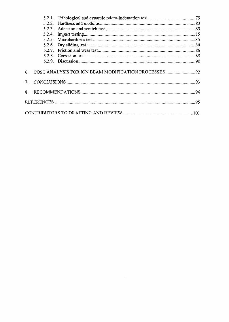
The subject of ion beam mixing deals with the compositional and structural changes oftwo or more component systems under the influence of an ion irradiation. Due to thesechanges, material properties of the system may be modified in ways sometimes difficult toachieve by conventional methods. From a collisional point of view, ion beam mixing relies onparticle-solid interaction. The phenomenon becomes more complex when thermodynamicalforces are involved, and these forces are sometimes modified by the presence of highconcentrations of defects in the system leading to various migration mechanism of atoms,such as Radiation Induced Segregation (RIS) or Radiation Enhanced Diffusion (RED).
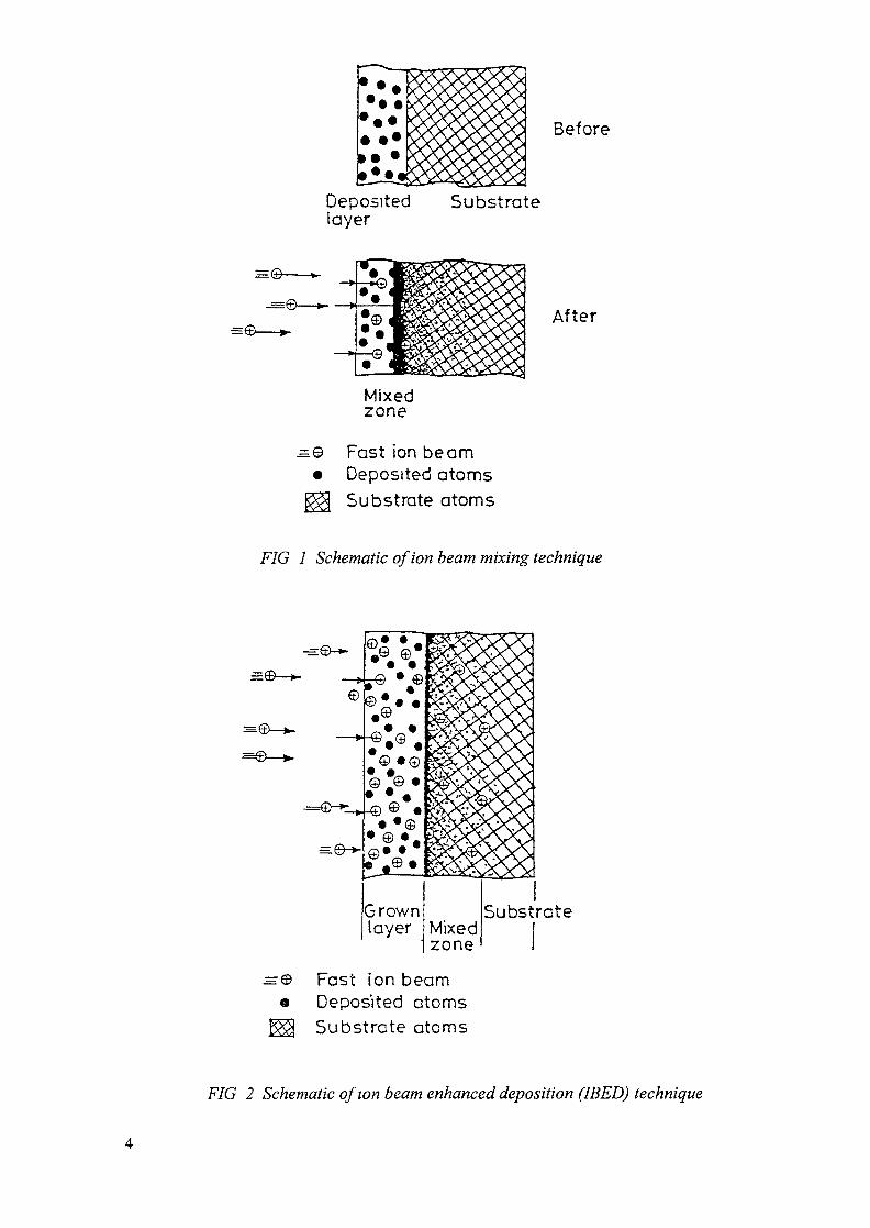
Ion beam mixing involves the use of energetic ion beams for driving and thereby"intermixing" the pre-deposited thin film atoms into substrates, via the dynamic collisioncascades produced by the penetrating ions. The process is schematically shown in Fig. 1.
The precursors of the work on ion beam mixing were studies of the preferentialsputtering of silicides where it was found that the composition changes occurred over thedepth of the bombarding ions. Aside from the influence of sputter depth profiling, there weresome indications that the ion induced reactions could be used for material modification. Fromthe technological point of view Ion beam Mixings offers an unique possibility to form almostany alloy of any composition and highly metastable, often amorphous, structure.
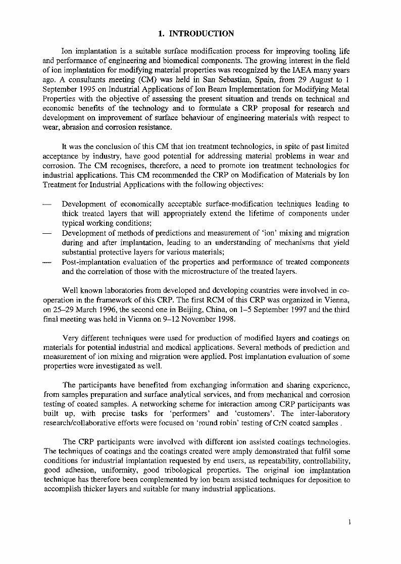
2.2. ION BEAM ASSISTED DEPOSITION (IB AD)
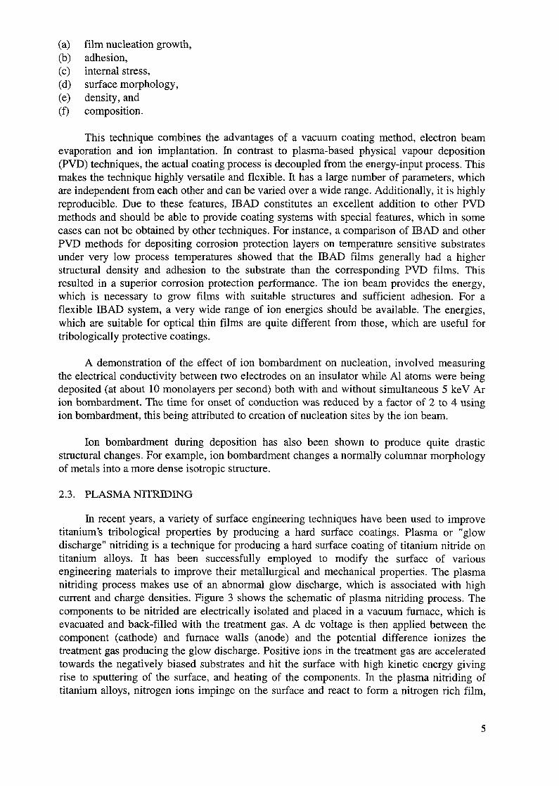
IB AD consists of simultaneously depositing the desired material using some evaporatingtechnique and bombarding by energetic ion beams. Schematic of the process is shown inFig. 2. This technique has been studied by a number of researchers for the purpose ofunderstanding the role of energetic ions in the conventional physical vapour deposition (PVD)processes. It has been recognized that the presence of energetic ions has a synergistic effect onthin film growth. There are several aspects of film growth that have been beneficiallyinfluenced by ion bombardment during thin film deposition including:
Before
Depositedlayer
Substrate
=©—*-
Mixedzone
,e Fast ion beam• Deposited atoms
Substrate atoms
After
FIG 1 Schematic of ion beam mixing technique
=e-*-
==©_».
Substrate
r© Fast ion beam« Deposited atoms
$® Substrate atoms
FIG 2 Schematic of ion beam enhanced deposition (IBED) technique
(a) film nucleation growth,(b) adhesion,(c) internal stress,(d) surface morphology,(e) density, and(f) composition.
This technique combines the advantages of a vacuum coating method, electron beamevaporation and ion implantation. In contrast to plasma-based physical vapour deposition(PVD) techniques, the actual coating process is decoupled from the energy-input process. Thismakes the technique highly versatile and flexible. It has a large number of parameters, whichare independent from each other and can be varied over a wide range. Additionally, it is highlyreproducible. Due to these features, IBAD constitutes an excellent addition to other PVDmethods and should be able to provide coating systems with special features, which in somecases can not be obtained by other techniques. For instance, a comparison of IBAD and otherPVD methods for depositing corrosion protection layers on temperature sensitive substratesunder very low process temperatures showed that the IBAD films generally had a higherstructural density and adhesion to the substrate than the corresponding PVD films. Thisresulted in a superior corrosion protection performance. The ion beam provides the energy,which is necessary to grow films with suitable structures and sufficient adhesion. For aflexible IBAD system, a very wide range of ion energies should be available. The energies,which are suitable for optical thin films are quite different from those, which are useful fortribologically protective coatings.
A demonstration of the effect of ion bombardment on nucleation, involved measuringthe electrical conductivity between two electrodes on an insulator while Al atoms were beingdeposited (at about 10 monolayers per second) both with and without simultaneous 5 keV Arion bombardment. The time for onset of conduction was reduced by a factor of 2 to 4 usingion bombardment, this being attributed to creation of nucleation sites by the ion beam.
Ion bombardment during deposition has also been shown to produce quite drasticstructural changes. For example, ion bombardment changes a normally columnar morphologyof metals into a more dense isotropic structure.
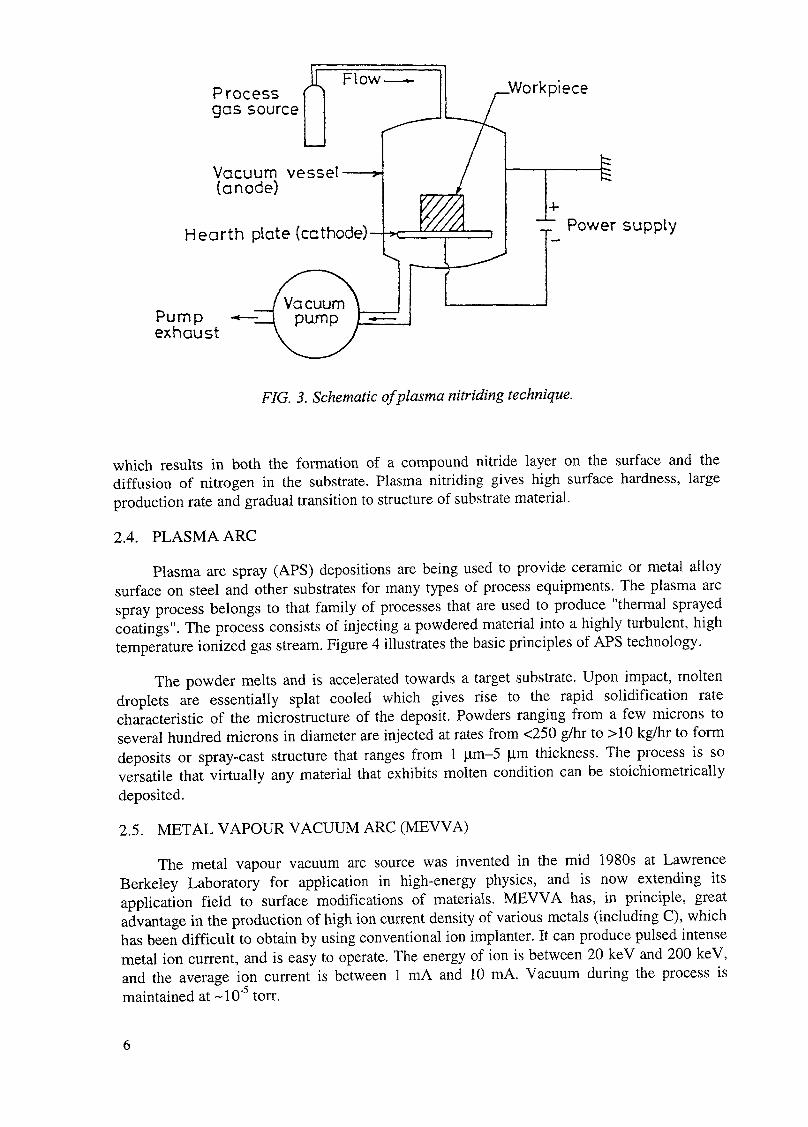
2.3. PLASMA NITRIDING
In recent years, a variety of surface engineering techniques have been used to improvetitanium's tribological properties by producing a hard surface coatings. Plasma or "glowdischarge" nitriding is a technique for producing a hard surface coating of titanium nitride ontitanium alloys. It has been successfully employed to modify the surface of variousengineering materials to improve their metallurgical and mechanical properties. The plasmanitriding process makes use of an abnormal glow discharge, which is associated with highcurrent and charge densities. Figure 3 shows the schematic of plasma nitriding process. Thecomponents to be nitrided are electrically isolated and placed in a vacuum furnace, which isevacuated and back-filled with the treatment gas. A dc voltage is then applied between thecomponent (cathode) and furnace walls (anode) and the potential difference ionizes thetreatment gas producing the glow discharge. Positive ions in the treatment gas are acceleratedtowards the negatively biased substrates and hit the surface with high kinetic energy givingrise to sputtering of the surface, and heating of the components. In the plasma nitriding oftitanium alloys, nitrogen ions impinge on the surface and react to form a nitrogen rich film,
Processgas source
Vacuum vessel(anode)
.Workpiece
Pumpexhaust
Hearth plate (cathode) Power supply
FIG. 3. Schematic of plasma nitriding technique.
which results in both the formation of a compound nitride layer on the surface and thediffusion of nitrogen in the substrate. Plasma nitriding gives high surface hardness, largeproduction rate and gradual transition to structure of substrate material.
2.4. PLASMA ARC
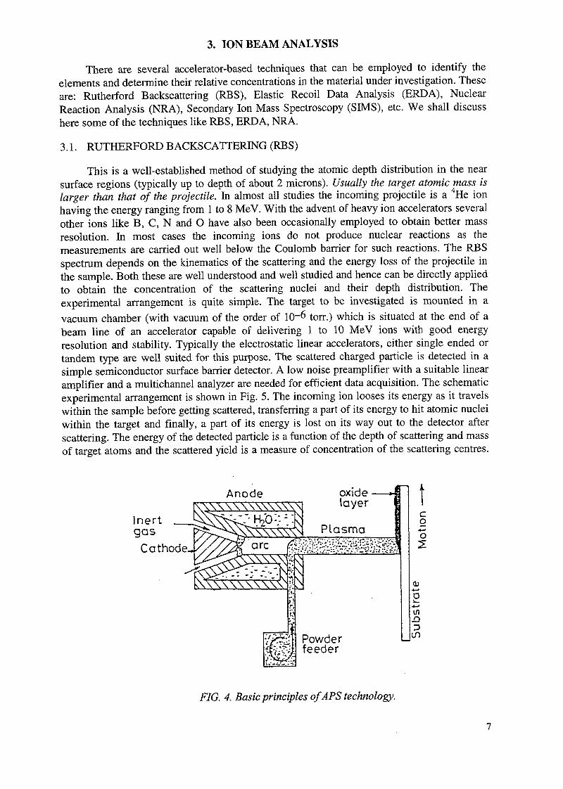
Plasma arc spray (APS) depositions are being used to provide ceramic or metal alloysurface on steel and other substrates for many types of process equipments. The plasma arcspray process belongs to that family of processes that are used to produce "thermal sprayedcoatings". The process consists of injecting a powdered material into a highly turbulent, hightemperature ionized gas stream. Figure 4 illustrates the basic principles of APS technology.
The powder melts and is accelerated towards a target substrate. Upon impact, moltendroplets are essentially splat cooled which gives rise to the rapid solidification ratecharacteristic of the microstructure of the deposit. Powders ranging from a few microns toseveral hundred microns in diameter are injected at rates from <250 g/hr to >10 kg/hr to formdeposits or spray-cast structure that ranges from 1 ^m-5 |im thickness. The process is soversatile that virtually any material that exhibits molten condition can be stoichiometricallydeposited.
2.5. METAL VAPOUR VACUUM ARC (MEWA)The metal vapour vacuum arc source was invented in the mid 1980s at Lawrence
Berkeley Laboratory for application in high-energy physics, and is now extending itsapplication field to surface modifications of materials. MEVVA has, in principle, greatadvantage in the production of high ion current density of various metals (including C), whichhas been difficult to obtain by using conventional ion implanter. It can produce pulsed intensemetal ion current, and is easy to operate. The energy of ion is between 20 keV and 200 keV,and the average ion current is between 1 mA and 10 mA. Vacuum during the process ismaintained at -10" torr.
3. ION BEAM ANALYSIS
There are several accelerator-based techniques that can be employed to identify theelements and determine their relative concentrations in the material under investigation. Theseare: Rutherford Backscattering (RBS), Elastic Recoil Data Analysis (ERDA), NuclearReaction Analysis (NRA), Secondary Ion Mass Spectroscopy (SIMS), etc. We shall discusshere some of the techniques like RBS, ERDA, NRA.
3.1. RUTHERFORD BACKSCATTERING (RBS)
This is a well-established method of studying the atomic depth distribution in the nearsurface regions (typically up to depth of about 2 microns). Usually the target atomic mass islarger than that of the projectile. In almost all studies the incoming projectile is a 4He ionhaving the energy ranging from 1 to 8 MeV. With the advent of heavy ion accelerators severalother ions like B, C, N and O have also been occasionally employed to obtain better massresolution. In most cases the incoming ions do not produce nuclear reactions as themeasurements are carried out well below the Coulomb barrier for such reactions. The RBSspectrum depends on the kinematics of the scattering and the energy loss of the projectile inthe sample. Both these are well understood and well studied and hence can be directly appliedto obtain the concentration of the scattering nuclei and their depth distribution. Theexperimental arrangement is quite simple. The target to be investigated is mounted in avacuum chamber (with vacuum of the order of 10~6 torr.) which is situated at the end of abeam line of an accelerator capable of delivering 1 to 10 MeV ions with good energyresolution and stability. Typically the electrostatic linear accelerators, either single ended ortandem type are well suited for this purpose. The scattered charged particle is detected in asimple semiconductor surface barrier detector. A low noise preamplifier with a suitable linearamplifier and a multichannel analyzer are needed for efficient data acquisition. The schematicexperimental arrangement is shown in Fig. 5. The incoming ion looses its energy as it travelswithin the sample before getting scattered, transferring a part of its energy to hit atomic nucleiwithin the target and finally, a part of its energy is lost on its way out to the detector afterscattering. The energy of the detected particle is a function of the depth of scattering and massof target atoms and the scattered yield is a measure of concentration of the scattering centres.
Anode
Inertgas
Cathode.
oxidelayer
Plasma
Powderfeeder
co
0)4_*
O•t—'IftnDl-O
FIG. 4. Basic principles of APS technology.

Ion Beam Target(M2,Z2)
Detector
FIG. 5. Schematic ofRBS experimental arrangement.
Let EO be the energy of the incident particle of mass M] and EI be the energy of the particleat the time of scattering. Then the energy £2 of the particle immediately after scattering by atarget atom of mass M2 is given by:
where the kinematical factor K is obtained from the relation
TV- __
-ill 2
M,+M 2(2)
for M}<M2 and for scattering angle 0.
The final energy £3 of the detected particle is:
£3 = E2-t2 (dE/dx)E2
with £2 = KEi = K[E()-ti (dE/dx)EQ]
(3)
(4)
tj and t2 being the distances traversed by the projectile in the sample before and after thescattering respectively. In these expressions (dE/dx) is the energy loss of the projectile at theindicated energy, which are extensively tabulated. Thus, knowing EQ, £3, MI, M2 and 9, thedepth at which the scattering centre is located can be determined. The RBS scattering cross-section, for scattering angle 9, is given by:
,mo(6)= 4 ( 6 'Cosec - (5)
Z} and Z2 being the atomic numbers of the projectile and the scattering atom respectively.The yield of scattered projectile is proportional to the scattering cross-section. Thus, by

measuring the relative yields of particles scattered from various atomic species at same depthone can easily determine their relative concentrations. A typical RBS spectrum is shown inFig. 6.
1000
IT,I—z:13OCJ
QLJ
Oz
100
0
i——'——rAl(Sb)
AS IMPLANTED
RUBBED 12 TIMES' •'!" i-WITH 5/0 EMERY i '
1100 200 300 400 500 '600 700 800 900
C H A N N E L N U M B E R
FIG. 6. RBS spectrum of as implanted FeSb sample.
3.2. ELASTIC RECOIL DETECTION ANALYSIS (ERDA)
RBS is suitable if the probe atoms are heavier than the projectile ions. In the case oflighter atoms, the technique of elastic recoil detection analysis (ERDA) can be employed.Here, the incident projectile ion causes the target atom to recoil in the forward direction.Figure? shows the geometrical arrangement of the experimental set up. The atoms ofdifferent masses recoil with different energies and hence can be separated out in the recoilenergy spectrum. The recoil energy, ER , is given by:
ER 4 m P m T „ 2————3~Cos(mP +m-r}
(6)
where <j) is the laboratory angle at which the recoil is detected and Ep is the projectile energy.The energy of the recoils from various depths of the sample is determined by two factors: (i)the rate of energy loss (dE/dx)jn of the incident ion in the target, and (ii) the rate of energy loss
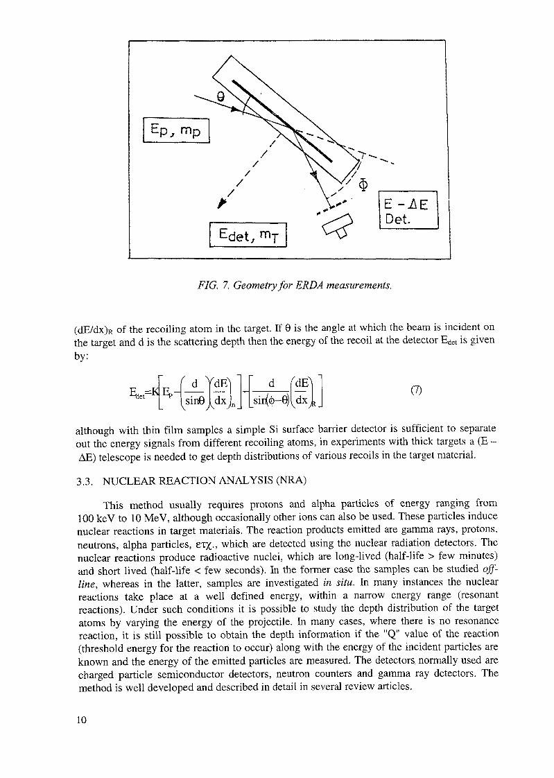
E-AEDet
FIG. 7. Geometry for ERDA measurements.
(dE/dx)R of the recoiling atom in the target. If 6 is the angle at which the beam is incident onthe target and d is the scattering depth then the energy of the recoil at the detector Edet is givenby:
(7)sir((j)-0Hdx
although with thin film samples a simple Si surface barrier detector is sufficient to separateout the energy signals from different recoiling atoms, in experiments with thick targets a (E -AE) telescope is needed to get depth distributions of various recoils in the target material.
3.3. NUCLEAR REACTION ANALYSIS (NRA)
This method usually requires protons and alpha particles of energy ranging from100 keV to 10 MeV, although occasionally other ions can also be used. These particles inducenuclear reactions in target materials. The reaction products emitted are gamma rays, protons,neutrons, alpha particles, et%., which are detected using the nuclear radiation detectors. Thenuclear reactions produce radioactive nuclei, which are long-lived (half-life > few minutes)and short lived (half-life < few seconds). In the former case the samples can be studied off-line, whereas in the latter, samples are investigated in situ. In many instances the nuclearreactions take place at a well defined energy, within a narrow energy range (resonantreactions). Under such conditions it is possible to study the depth distribution of the targetatoms by varying the energy of the projectile. In many cases, where there is no resonancereaction, it is still possible to obtain the depth information if the "Q" value of the reaction(threshold energy for the reaction to occur) along with the energy of the incident particles areknown and the energy of the emitted particles are measured. The detectors, normally used arecharged particle semiconductor detectors, neutron counters and gamma ray detectors. Themethod is well developed and described in detail in several review articles.
10

In the case of nuclear reactions producing long lived radioactive nuclei, the yield of theproduct is given by the expression:
N0 = a n p p X t (8)A
where a is the reaction cross-section in cm , np is the number of incident ions per second, p isthe number density of the atomic species in the target (atoms/cc), X is the effective targetthickness in cms., and t is the time of irradiation in seconds. Here by effective target thicknesswe mean the thickness throughout which the reaction can take place. The factor (p X) willtherefore be expressed in the units of ats./cm2. The well known radioactive decay law givesthe number of radioactive nuclei at any time ti, after stopping the irradiation:
N(t,) = No(l-exp(-A,t,)) (9)
A, being the decay constant for the radioactive nuclei produced in the reaction.
The decaying radioactive nuclei, in general, emit characteristic gamma rays. Theenergies of these gamma rays are tabulated extensively. Thus, by measuring the intensities ofthe specific gamma rays and using eqns. 6 and 7, value of p can be extracted even in case ofextremely low concentrations. Another application of this method is in the study of wear andcorrosion properties of various materials. Here the residual radioactivity in the material, aftersubjecting it to corrosion and wear processes, are measured. Of course "hot laboratory"facilities for handling and disposal of radioactive materials are required.
4. EXPERIMENTAL WORK
This section describes the actual experimental details of the coating methods (i.e. themethods of sample preparation), characterization and the performance of the coated samples,with reference to mechanical, electrical, chemical and tribological properties.
4.1. Y ION IMPLANTATION ON ZrO2 CERAMICS
Zirconia ceramics were modified by Y ion implantation in a MEVVA implanter. Thesamples used for implantation were hot-pressed ZrOi ceramics, which were cut into 3 x 6 x40 mm3 bars, then polished to mirror finish with 0.5 micron diamond paste. It contained 90%tetragonal and 10% monoclinic phase. Its density was 6.05 g/cm3, and the grain size was onemicron. Before implantation all samples were carefully ultrasonically cleaned in acetone andmethanol. The Y ion implantation was carried out in a MEVVA source with an extractionvoltage of 60KV. The samples were implanted with an ion current density of 80 fjA/cm2 andthe ion doses ranged from 8 x 10¹⁵ to 1.8 x 10¹⁸ Y/ cm2. The samples were not cooled duringimplantation and their temperature rise was only due to ion bombarding.
The phase structure of as-implanted samples was determined by XPS and XRD. Themicrohardness, flexural strength and fracture toughness of as-implanted samples weremeasured. The fracture toughness was measured in the standard mode with a span of 24 mmand a loading velocity of 0.05 mm/min.
XRD and XPS analyses of implanted samples showed that there were basically T-ZrO2(tetragonal phase), M-ZrO2 (monoclinic phase), CeO2, and the ^2^3 phases in the implantedregion. Transformation of some of the T-ZrOa phase into M-ZrOa phase took place as dose of
11
implantation increased. Amorphization of ZrC>2 ceramics was also observed in the implanted17 Oregion after Y ion implantation at doses above 6x10 Y/cm .
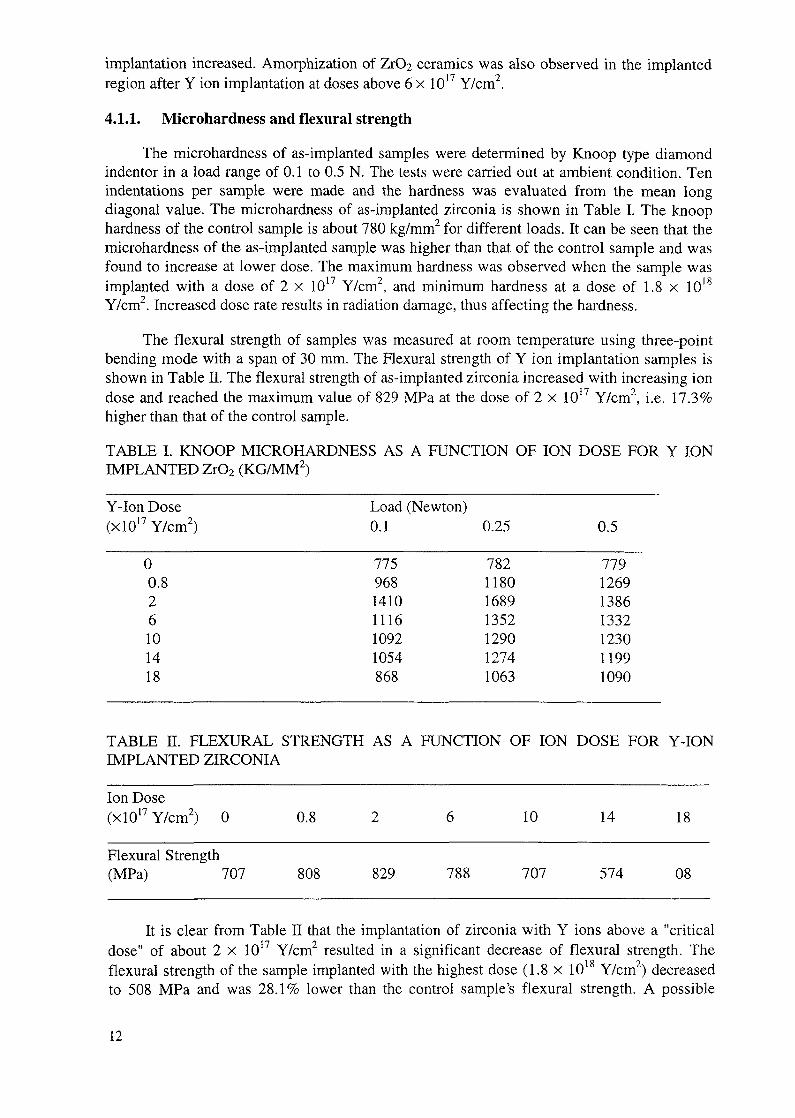
4.1.1. Microhardness and flexural strength
The microhardness of as-implanted samples were determined by Knoop type diamondindentor in a load range of 0.1 to 0.5 N. The tests were carried out at ambient condition. Tenindentations per sample were made and the hardness was evaluated from the mean longdiagonal value. The microhardness of as-implanted zirconia is shown in Table I. The knoophardness of the control sample is about 780 kg/mm2 for different loads. It can be seen that themicrohardness of the as-implanted sample was higher than that of the control sample and wasfound to increase at lower dose. The maximum hardness was observed when the sample wasimplanted with a dose of 2 x 10¹⁷ Y/cm2, and minimum hardness at a dose of 1.8 x 10¹⁸
Y/cm2. Increased dose rate results in radiation damage, thus affecting the hardness.
The flexural strength of samples was measured at room temperature using three-pointbending mode with a span of 30 mm. The Flexural strength of Y ion implantation samples isshown in Table n. The flexural strength of as-implanted zirconia increased with increasing iondose and reached the maximum value of 829 MPa at the dose of 2 x 10¹⁷ Y/cm2, i.e. 17.3%higher than that of the control sample.
TABLE I. KNOOP MICROHARDNESS AS A FUNCTION OF ION DOSE FOR Y IONIMPLANTED ZrO2 (KG/MM2)
Y-Ion Dose Load (Newton)(x!017Y/cm2) 0.1 0.25 0.5
0 775 782 7790.8 968 1180 12692 1410 1689 13866 1116 1352 133210 1092 1290 123014 1054 1274 119918 868 1063 1090
TABLE E. FLEXURAL STRENGTH AS A FUNCTION OF ION DOSE FOR Y-IONIMPLANTED ZIRCONIA
Ion Dose(x!017Y/cm2) 0 0.8 2 6 10 14 18
Flexural Strength(MPa) 707 808 829 788 707 574 08
It is clear from Table n that the implantation of zirconia with Y ions above a "criticaldose" of about 2 x 10¹⁷ Y/cm2 resulted in a significant decrease of flexural strength. The
1 o oflexural strength of the sample implanted with the highest dose (1.8 x 10 Y/cm ) decreasedto 508 MPa and was 28.1% lower than the control sample's flexural strength. A possible
12
explanation is that the radiation damage piled up and expanded with increasing ion dose, andfinally resulted in degradation of flexural strength. The dose dependence of the flexuralstrength of as-implanted samples was similar with that of microhardness of as-implantedsamples.
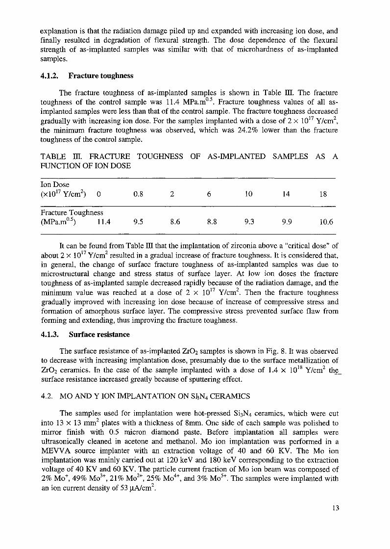
4.1.2. Fracture toughness
The fracture toughness of as-implanted samples is shown in Table ITJ. The fracturetoughness of the control sample was 11.4 MPa.m°'5. Fracture toughness values of all as-implanted samples were less than that of the control sample. The fracture toughness decreasedgradually with increasing ion dose. For the samples implanted with a dose of 2 x 10¹⁷ Y/cm2,the minimum fracture toughness was observed, which was 24.2% lower than the fracturetoughness of the control sample.
TABLE IE. FRACTURE TOUGHNESS OF AS-IMPLANTED SAMPLES AS AFUNCTION OF ION DOSE
Ion Dose(x!017Y/cm2) 0 0.8 2 6 10 14 18
Fracture Toughness(MPa.m05) 11.4 9.5 8.6 8.8 9.3 9.9 10.6
It can be found from Table in that the implantation of zirconia above a "critical dose" ofabout 2 x 10¹⁷ Y/cm2 resulted in a gradual increase of fracture toughness. It is considered that,in general, the change of surface fracture toughness of as-implanted samples was due tomicrostructural change and stress status of surface layer. At low ion doses the fracturetoughness of as-implanted sample decreased rapidly because of the radiation damage, and theminimum value was reached at a dose of 2 x 10¹⁷ Y/cm2. Then the fracture toughnessgradually improved with increasing ion dose because of increase of compressive stress andformation of amorphous surface layer. The compressive stress prevented surface flaw fromforming and extending, thus improving the fracture toughness.
4.1.3. Surface resistance
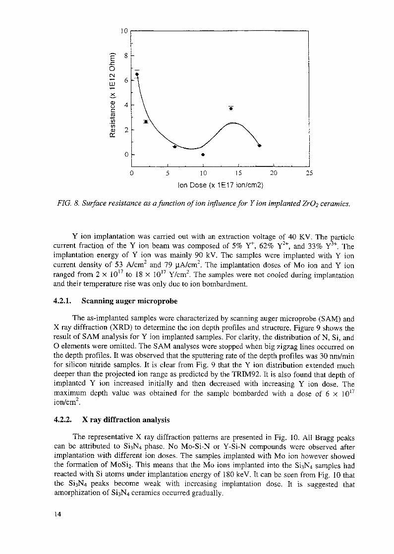
The surface resistance of as-implanted ZrO2 samples is shown in Fig. 8. It was observedto decrease with increasing implantation dose, presumably due to the surface metallization ofZrO2 ceramics. In the case of the sample implanted with a dose of 1.4 x 10¹⁸ Y/cm2 the_surface resistance increased greatly because of sputtering effect.
4.2. MO AND Y ION IMPLANTATION ON S^N4 CERAMICS
The samples used for implantation were hot-pressed Si-^4 ceramics, which were cutinto 13 x 13 mm2 plates with a thickness of 8mm. One side of each sample was polished tomirror finish with 0.5 micron diamond paste. Before implantation all samples wereultrasonically cleaned in acetone and methanol. Mo ion implantation was performed in aMEVVA source implanter with an extraction voltage of 40 and 60 KV. The Mo ionimplantation was mainly carried out at 120 keV and 180 keV corresponding to the extractionvoltage of 40 KV and 60 KV. The particle current fraction of Mo ion beam was composed of2% Mo+, 49% Mo3+, 21% Mo2+, 25% Mo4+, and 3% Mo5+. The samples were implanted withan ion current density of 53 |iA/cm2.
13
10
E.cOCM
(DOc
<u 2
5 10 15 20
Ion Dose (x 1E17 ion/cm2)25
FIG. 8. Surface resistance as a function of ion influence for Y ion implanted ZrO2 ceramics.
Y ion implantation was carried out with an extraction voltage of 40 KV. The particlecurrent fraction of the Y ion beam was composed of 5% Y+, 62% Y2+, and 33% Y3+. Theimplantation energy of Y ion was mainly 90 kV. The samples were implanted with Y ioncurrent density of 53 A/cm2 and 79 |iA/cm2. The implantation doses of Mo ion and Y ionranged from 2 x 10¹⁷ to 18 x 1017 Y/cm2. The samples were not cooled during implantationand their temperature rise was only due to ion bombardment.
4.2.1. Scanning auger microprobe
The as-implanted samples were characterized by scanning auger microprobe (SAM) andX ray diffraction (XRD) to determine the ion depth profiles and structure. Figure 9 shows theresult of SAM analysis for Y ion implanted samples. For clarity, the distribution of N, Si, andO elements were omitted. The SAM analyses were stopped when big zigzag lines occurred onthe depth profiles. It was observed that the sputtering rate of the depth profiles was 30 nm/minfor silicon nitride samples. It is clear from Fig. 9 that the Y ion distribution extended muchdeeper than the projected ion range as predicted by the TREVI92. It is also found that depth ofimplanted Y ion increased initially and then decreased with increasing Y ion dose. Themaximum depth value was obtained for the sample bombarded with a dose of 6 x 10¹⁷
ion/cm2.
4.2.2. X ray diffraction analysis
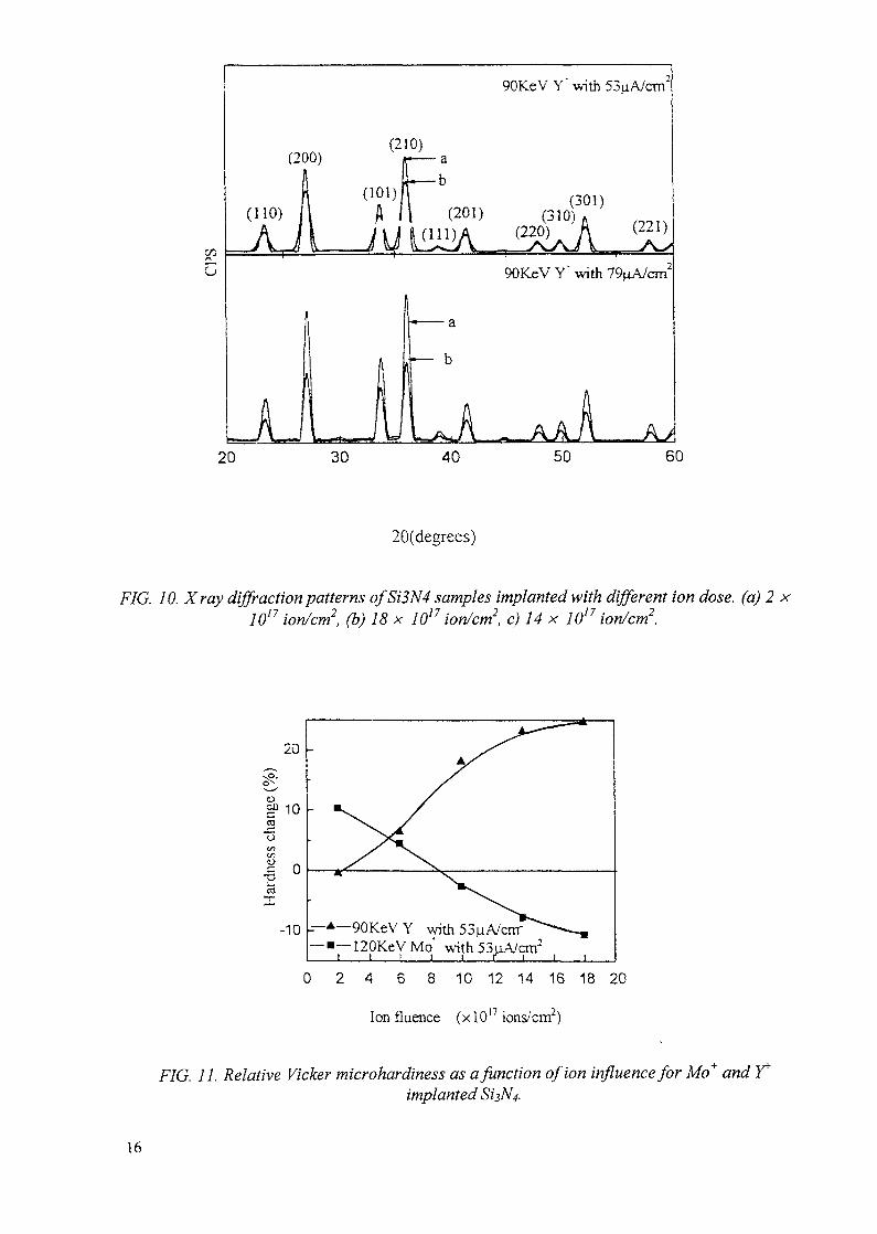
The representative X ray diffraction patterns are presented in Fig. 10. All Bragg peakscan be attributed to Si3N4 phase. No Mo-Si-N or Y-Si-N compounds were observed afterimplantation with different ion doses. The samples implanted with Mo ion however showedthe formation of MoSi2. This means that the Mo ions implanted into the Si3N4 samples hadreacted with Si atoms under implantation energy of 180 keV. It can be seen from Fig. 10 thatthe SislSU peaks become weak with increasing implantation dose. It is suggested thatamorphization of SislNU ceramics occurred gradually.
14
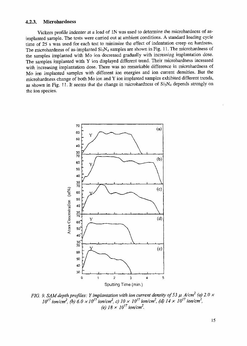
4.2.3. Microhardness
Vickers profile indenter at a load of IN was used to determine the microhardness of as-implanted sample. The tests were carried out at ambient conditions. A standard loading cycletime of 25 s was used for each test to minimize the effect of indentation creep on hardness.The microhardness of as-implanted Si3N4 samples are shown in Fig. 11. The microhardness ofthe samples implanted with Mo ion decreased gradually with increasing implantation dose.The samples implanted with Y ion displayed different trend. Their microhardness increasedwith increasing implantation dose. There was no remarkable difference in microhardness ofMo ion implanted samples with different ion energies and ion current densities. But themicrohardness change of both Mo ion and Y ion implanted samples exhibited different trends,as shown in Fig. 11. It seems that the change in microhardness of Si3N4 depends strongly onthe ion species.
EO
o<
70605040307060504030706050403070"60'50'40'30'7060504030
Y(a)
(b)
Y (d)
(e)
2 3Sputting Time (min.)
FIG. 9. SAM depth profiles: Y implantation with ion current density of 53 ju A/cm2 (a) 2.0 x10¹⁷ ion/cm2, (b) 6.0 x!0n ion/cm2, c) 10 x 1017 ion/cm2, (d) 14 x 1017 ion/cm2,
(e) 18 x 1017 ion/cm2.
15
(200)
90KeV Y" with 53uA/cm
(210)
(201)(301)
(310)(220) (221)
90KeV Y" with 79nA/cm
- a
b
A20 30 40 50 60
28(degrees)
FIG. 10. Xray diffraction patterns ofSi3N4 samples implanted with different ion dose, (a) 2 x10¹⁷ ion/cm2, (b) 18 x 1017 ion/cm2, c) 14 x 1017 ion/cm2.
\--+~90KeVY with53nA/cnr—•—120KeVMo' with 53u.A/cm2
0 24 6 8 10 12 14 16 18 20
Ion fluence (x 1017 ions/cm2)
FIG. 11. Relative Vicker microhardiness as a function of ion influence for Mo+ andimplanted SisN^
16
4.2.4. Sheet resistance
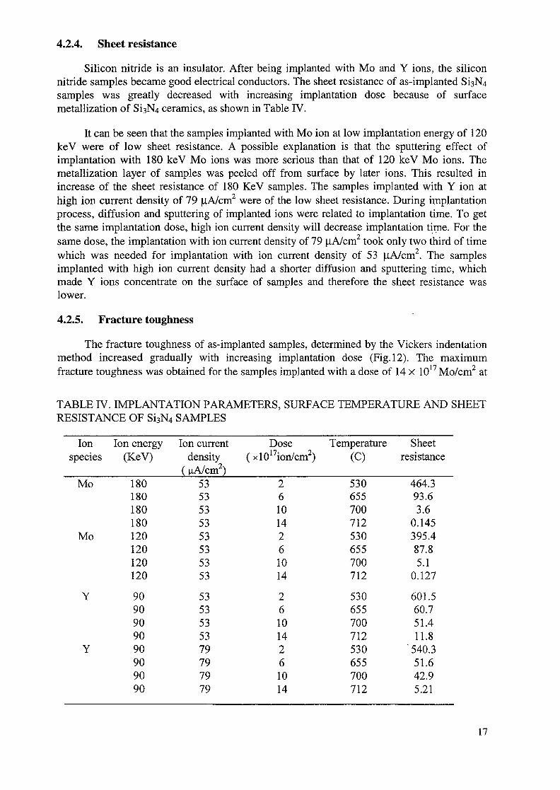
Silicon nitride is an insulator. After being implanted with Mo and Y ions, the siliconnitride samples became good electrical conductors. The sheet resistance of as-implanted $13^4samples was greatly decreased with increasing implantation dose because of surfacemetallization of 813 ceramics, as shown in Table IV.
It can be seen that the samples implanted with Mo ion at low implantation energy of 120keV were of low sheet resistance. A possible explanation is that the sputtering effect ofimplantation with 180 keV Mo ions was more serious than that of 120 keV Mo ions. Themetallization layer of samples was peeled off from surface by later ions. This resulted inincrease of the sheet resistance of 180 KeV samples. The samples implanted with Y ion athigh ion current density of 79 joA/cm2 were of the low sheet resistance. During implantationprocess, diffusion and sputtering of implanted ions were related to implantation time. To getthe same implantation dose, high ion current density will decrease implantation time. For thesame dose, the implantation with ion current density of 79 |iA/cm2 took only two third of timewhich was needed for implantation with ion current density of 53 |iA/cm2. The samplesimplanted with high ion current density had a shorter diffusion and sputtering time, whichmade Y ions concentrate on the surface of samples and therefore the sheet resistance waslower.
4.2.5. Fracture toughness
The fracture toughness of as-implanted samples, determined by the Vickers indentationmethod increased gradually with increasing implantation dose (Fig. 12). The maximumfracture toughness was obtained for the samples implanted with a dose of 14 x 1017 Mo/cm2 at
TABLE IV. IMPLANTATION PARAMETERS, SURFACE TEMPERATURE AND SHEETRESISTANCE OF Si3N4 SAMPLES
Ionspecies
Mo
Mo
Y
Y
Ion energy(KeV)
180180180180120120120120
9090909090909090
Ion currentdensity
( ^A/cm2)5353535353535353
5353535379797979
Dose(xl017ion/cm2)
261014261014
261014261014
Temperature(C)
530655700712530655700712
530655700712530655700712
Sheetresistance
464.393.63.6
0.145395.487.85.1
0.127
601.560.751.411.8
" 540.351.642.95.21
17

180 keV. It was 35.9% higher than that of the control sample. Comparing the implantationparameters, ion energy seems to play an important role in the improvement of fracturetoughness of Si^N^. The implantation ion current density of Y ions does not seem to improvethe fracture toughness. It is considered in general that improvement of fracture toughness ofas-implanted samples is due to compressive stress resulting from ion implantation, and thecompressive stress increased with increasing implantation dose.
4.3. PARTICLE MIGRATION IN THE NI/AL MULTILAYERS
The Ni/Al multilayer with alternating Ni (25 nm) and Al (36 nm) layers was sputterdeposited on smooth silicon substrate using a Balzers Sputron Plasma System. The averagecomposition of the multilayer was Nio.sAlo.s with a total thickness of 315 nm. After thedeposition, the multilayer was ion treated at different temperatures, in the range between -145°C and +430°C. Ion irradiation of NiAl multilayers was performed in a Balzers MPB
\f\ *)202 RR implanter using 350 keV Ar ions and a dose of 1 x 10 Ar/cm .
4.3.1. Auger electron spectrometry (AES)
The Ni/Al multilayers were ion treated at different temperatures. All these samples werecharacterized with AES depth profiling. The PHI 545A scanning Auger microprobe with a
30 -
t, 15
V.o
30-f
15--
0
-*— ISOKeVMo with53uA/crrr120KeVMo" with53uA/cm2
—*-90KeVY
—v—90KeV Y' with79|iA/cnri_ j__i__i__i__ i__i__[_0 2 4 6 8 10 12 14 16 18 20
Ion fluence (xl017ions/cm2)
FIG. 12. Relative indentation fracture toughness as a function of ion influence for Mo+ andY* implanted Si^N4.
18
static primary electron beam of 3 keV, IjiA and a diameter of about 40 |im was used. Thesamples were ion sputtered by using two symmetrically inclined ion guns. The ion incidenceangle was 47° with respect to the normal to the sample surface. The samples were ionsputtered with IkeV Ar+ ion beam, rastered across an area of 10 x 10mm2.
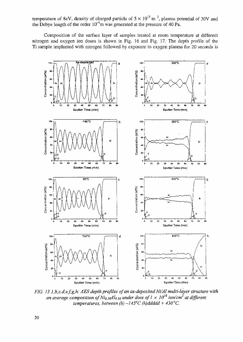
Fig. 13a shows the AES depth profile of the as-deposited Ni/Al multilayer with anaverage composition of Nio.sAlo.5. Ni is present in the Al thin films even though the sampletemperature during the deposition of Ni/Al multilayer was less than 100°C. We thereforeconclude that Ni is the main moving element in the early stage of diffusion. However, despitehigh depth resolution provided by two ion guns, it is not possible to exclude topographiceffect completely as they might cause a slight loss of depth resolution especially in the Al thinfilms.
The AES depth profile of the Ni/Al multilayers ion mixed at two different temperaturesof -145°C (Fig. 13b) and 25°C (Fig. 13c) shows almost the same concentration profiles. Inboth cases the migration of Ni and Al atoms is only enhanced by 350 keV Ar ion mixing. Asexpected, the thermally activated diffusion processes are negligible up to the roomtemperature. However, the effect of ion beam mixing is increased by thermally activatedmigration already in the sample heated at 130°C (Fig. 13d) and especially at highertemperatures of 230°C (Fig. 13e), 280°C (Fig. 13f), 330°C (Fig. 13g) and 430°C (Fig. 13h).Generally, temperature effect of ion beam mixing increased with increasing temperature. Theperiodicity of the Ni and Al concentration profiles is lost in the samples isothermally heattreated during ion mixing at 280°C and 330°C respectively. The ion mixing and diffusionprocess enhanced the migration of Ni and Al atoms and accelerated the formation of NiAlsolid solutions. The Ni/Al sample heated at 430°C show the completely reacted NiAl layerwith the composition of about 55.0 at% Al and 45.0 at% Ni.
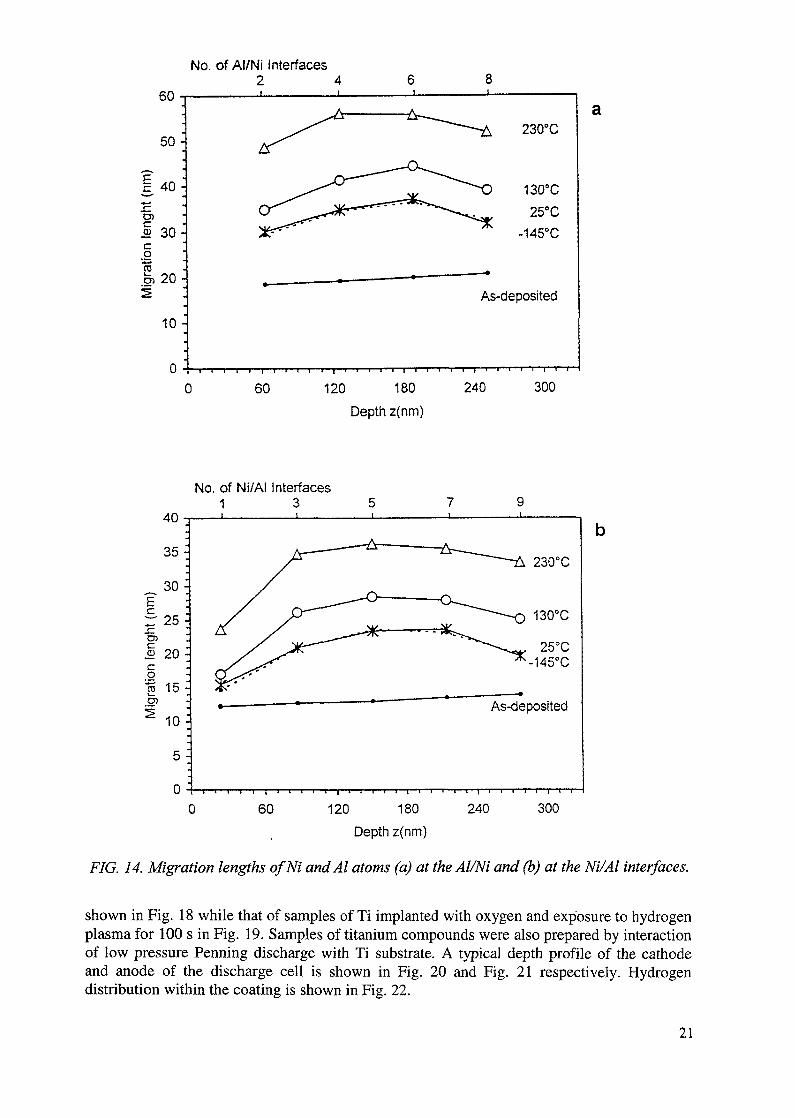
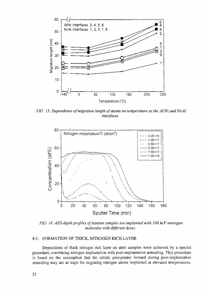
A detailed observation of the interface widths revealed different migration lengths of Niand Al atoms at the Ni/Al and Al/Ni interfaces in the ion and heat-treated Ni/Al multilayerstructures. The interface width was extracted from the amplitudes of the profile. The longermigration lengths were observed at the Al/Ni (Fig. 14a) than at the Ni/Al interfaces (Fig. 14b)located inside of the Ni/Al multilayer. This is the consequence of higher diffusion rate of Nithan Al atoms and of the ion range, which was estimated to be 180 nm with the TRIM 95code. With increasing temperature the interface widths increased additionally due to thermallyenhanced diffusion of Ni and Al atoms (Fig. 15).
4.4. INVESTIGATION OF INTERACTION OF GASEOUS IONS WITH GETTERMATERIAL
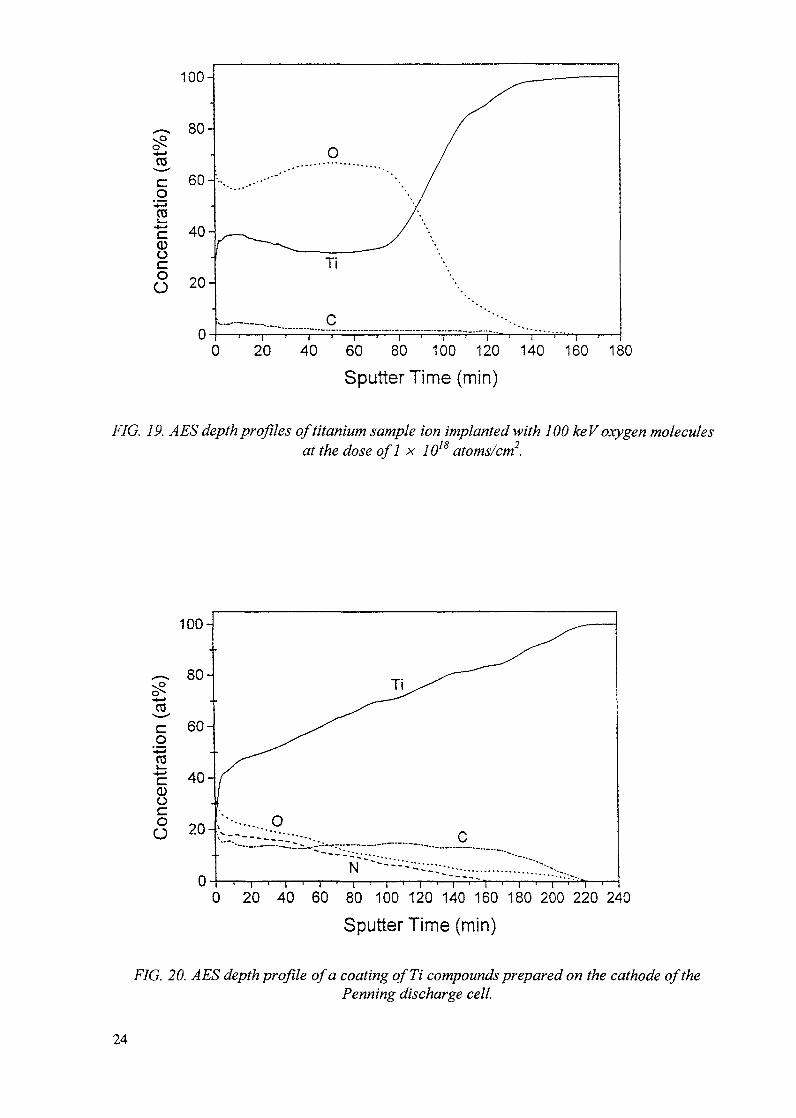
Samples of pure Ti plates were polished and exposed to a flux of nitrogen, oxygen andmethane ions with the kinetic energy of 100 keV per molecule. The ion doses were 5 x 1016,1 x 1017, 2.5 x 10¹⁷, 5 x 10¹⁷, 7.5 x 10¹⁷ and 1 x 10¹⁸ atoms/cm2. The ion implantation wasperformed at the Institute of Electronic Material Technology, Warsaw, Poland. Thecomposition of the surface layer on the samples has been determined with the AES method.Depth profiles have been obtained for both the ion implanted samples at room temperatureand the samples implanted at 400°C. Samples were then exposed to weakly ionized highlydissociated hydrogen or oxygen plasma, which was created by RF generator with thefrequency of 27.12 MHz and the power of 300W. Hydrogen plasma with electron temperatureof 6eV, density of charged particle of 1016 irf3, plasma potential of 20V and the Debye lengthof the order lO^m was generated at the pressure of 100 Pa. Oxygen plasma with the electron
19
temperature of 8eV, density of charged particle of 5 x 10¹⁵ m 3, plasma potential of 30V andthe Debye length of the order lO^m was generated at the pressure of 40 Pa.
Composition of the surface layer of samples treated at room temperature at differentnitrogen and oxygen ion doses is shown in Fig. 16 and Fig. 17. The depth profile of theTi sample implanted with nitrogen followed by exposure to oxygen plasma for 20 seconds is
Coo
rr 23CTC
10 JO 30 40 SO 60 70 K 80
Sputter Time (min)10 20 30 40 50 tO 70 10 *3
Sputter Time (mm)
280°C
10 10 M 40 SO «0 TO Ut M
Sputter Tim* (mln)
oo
0 10 20 JO 40 SO M TO 10 »0
Sputter Time (rmn|
8
10 20 30 40 50 60 70 »C 90
Sputter Time (min)
0 10 20 30 40 SO 60 70 SO 90
Sputter Time (min)
10 20 30 40 50 «0 70 SO 90
Sputter Time (min)
10 20 30 40 50 60 70 80 90
Sputter Time (min)
FIG. 13 1 ,b,c,d,e,f,g,h: AES depth profiles of an as-deposited Ni/Al multi-layer structure withan average composition ofNio.soAloso under dose of 1 x 10 ion/cm at different
temperatures, between (b) -145°C (h)ddddd + 430°C.
20
No. of AI/Ni Interfaces2 4
60 ———————i———————i-
50-
en§ 30Hc.
"rora 20 -!is
10 H
o60 120 180
Depth z(nm)
230°C
130°C25°C
-145°C
As-deposited
240 300
No. of Ni/AI Interfaces1 3
40
35:
30-
r 25:^r HenS 20-g
"ro 15 :
o>
5 -
00
230°C
130°C
25°C-145°C
As-deposited
60 120 180 240
Depth z(nm)300
FIG. 14. Migration lengths ofNi andAl atoms (a) at the Al/Ni and (b) at the Ni/AI interfaces.
shown in Fig. 18 while that of samples of Ti implanted with oxygen and exposure to hydrogenplasma for 100 s in Fig. 19. Samples of titanium compounds were also prepared by interactionof low pressure Penning discharge with Ti substrate. A typical depth profile of the cathodeand anode of the discharge cell is shown in Fig. 20 and Fig. 21 respectively. Hydrogendistribution within the coating is shown in Fig. 22.
21
Ai/Ni Interfaces 2, 4, 6, 8Ni/Al Interfaces 1, 3, 5, 7, 9
-145 50 100 150
Temperature (°C)
200 250
FIG 15. Dependence of migration length of atoms on temperature at the Al/Ni and Ni/Alinterfaces.
80-
60-
I 40 HTO
c<DOCOO
20-
0
Nitrogen implantatton/Ti (at/cm )
\
0 20 40 60 80 100 120 140 160 180Sputter Time (min)
FIG 16 AES depth profiles ofitanium samples ion implanted with 100 keV notrogenmolecules with different doses
4.5. FORMATION OF THICK, NITROGEN RICH LAYER
Depositions of thick nitrogen rich layer on steel samples were achieved by a specialprocedure, combining nitrogen implantation with post-implantation annealing. This procedureis based on the assumption that the nitride precipitates formed during post-implantationannealing may act as traps for migrating nitrogen atoms implanted at elevated temperatures.
22

The proposed procedure assumes the use of a typical ion implanter i. e. a machine delivering anon-separated nitrogen beam with energy up to 150 keV. The procedure is composed of foursteps: pre-implantation, formation of e-Fe3_xN precipitates, their transformation into y'-Fe4Nphase, and post-implantation at elevated temperatures which leads to a growth of y'-Fe4Nprecipitates ensuring the increase of the thickness of doped layer. The final process parametersare listed in Table V.
80
60-
to
•2 40-03v_'c0)o§ 20O
Oxygen implantation/Ti (at/cm )
0 20 40 60 80 100 120 140 160 180Sputter Time (min)
FIG. 17. AES depth profiles of titanium samples ion implanted with 100 keVoxygenmolecules with different doses.
100-
0 20 40 60 80 100 120 140 160 180Sputter Time (min)
FIG. 18. AES depth profiles of titanium samples ion implanted with 100 keV nitrogenIft "Jmolecules at the dose ofl x 10 atoms/cm .
23
100-
0 20 40 60 80 100 120 140 160 180Sputter Time (min)
FIG. 19. AES depth profiles of titanium sample ion implanted with 100 keVoxygen moleculesat the dose oflx 1018 atoms/cm2.
100-
00 20 40 60 80 100 120 140 160 180 200 220 240
Sputter Time (min)
FIG. 20. AES depth profile of a coating ofTi compounds prepared on the cathode of thePenning discharge cell
24
100-
0 20 40 60 80 100 120 140 160 180 200Sputter Time (min)
FIG. 21. AES depth profile of a coating ofTi compounds prepared on the anode of thePenning discharge cell
12-
cs1-"roX.co"ro"coocoO
10-
8-
6-
4-
2-
25 125 15050 75 100
Thickness (nm)
FIG. 22. Hydrogen concentration in the surface layer of the cathode of a Penning cell.
TABLE V. DESCRIPTION OF THE SAMPLE PREPARATION
Stepa) 1st implantationb) Annealingc) Post-annealingd) 2nd implantation
Process description2.1xl017N2
+, ISOkeV, RT200°C Ih + 250°C Ih + 300°C Ih350°C, 4.5h2xlQ1 7 N2
+, 70 keV, 200°C
25
4.5.1. Wear test
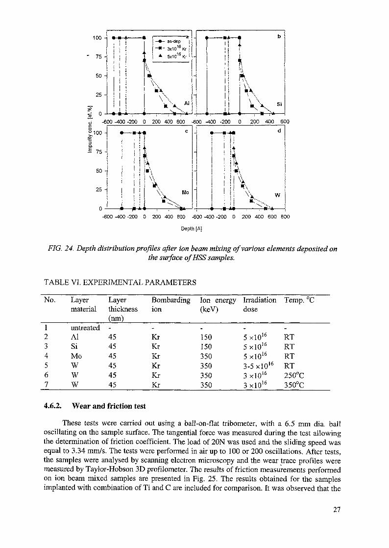
The wear tests were performed using a ball-on-flat tribotester with a 6.5 mm steel ball ascounter sample. The nominal load was equal to 20N, stroke was set to 3 mm and the averagespeed of translation amounted to 3.34 mm/s. The results of friction measurements arepresented in Fig. 23. The results obtained point to significant increase of friction coefficientwith processing temperature. This is especially important in the case of post-implantationcarried out at 200°C or 300°C. The value of friction coefficient measured on the samplesimplanted at elevated temperatures exceeds even the value recorded for the untreated HSSsteel samples (fs ~ 0.8).
4.6. FORMATION OF THICK, WEAR-RESISTANT METALLIC LAYERS VIA IONBEAM MIXING TECHNIQUE
Deposition of wear resistant metallic layer on high speed steel samples covered with Al,Si, Mo, and W were carried out by ion beam mixing method. The mixing processes werecarried out at temperatures ranging from room temperature to 350 C. The final processparameters are listed in Table VI.
4.6.1. Auger electron spectrometry (AES)
The depth distributions of doping elements before and after ion beam mixing processcarried out at room temperatures are shown in Fig. 24. One can note that the impurity profilesextend from the interface to the depth of few hundred angstroms, i.e. the depth comparable tothe projected range of implanted atoms in typical medium energy process. The increase ofprocess temperature does not result in significant increase of the thickness of impurity richlayer but rather in the increase of impurity concentration.
1.2-1 ' RT implantedRT + annealedRT+ann +11 200RT+ann +1! 300
0 10 20 30 40 50 60 70 80 90 100Number of cydes
FIG. 23. Friction coefficient changes during wear text.
26
100 -
- 75 -
50 -
25 -
P* n .
1
— t
M
t~l
»-4 ——— «;
t
i
i— —— t
i
L
1
\\•
A''
\
-«~ as-dep-•- 3x1016Kr* 5x1016Kr ,
^\•X
k'"'* A1
v "•-..
-
-
(
__-J
» ——— 1
k ————— 1
IA —— 4j
i
LA. ——— 1
b
1\\
\•X
'. **,
V \ St•m 'X-A
d -600 -400 -200 0 200 400 600 -600 -400 -200 0 200 400 600
Q.- 75 -I
50 -
25 -
0 IMo
- ifc*-
I*m
W
-600 -400 -200 0 200 400 600 -600 -400 -200 0 200 400 600 800
Depth [A]
FIG, 24, Depth distribution profiles after ion beam mixing of various elements deposited onthe surface ofHSS samples.
TABLE VI. EXPERIMENTAL PARAMETERS
No.
1234561
Layermaterial
untreatedAlSiMoWWW
Layerthickness(nm)_454545454545
Bombardingion
.KrKrKrKrKrKr
Ion energy(keV)
.150150350350350350
Irradiationdose
_5xl016
5xl01 6
5xl01 6
3-5 xlO16
3xl016
3xl01 6
Temp. °C
_RTRTRTRT250°C350°C
4.6.2. Wear and friction test
These tests were carried out using a ball-on-flat tribometer, with a 6.5 mm dia. balloscillating on the sample surface. The tangential force was measured during the test allowingthe determination of friction coefficient. The load of 20N was used and the sliding speed wasequal to 3.34 mm/s. The tests were performed in air up to 100 or 200 oscillations. After tests,the samples were analysed by scanning electron microscopy and the wear trace profiles weremeasured by Taylor-Hobson 3D profilometer. The results of friction measurements performedon ion beam mixed samples are presented in Fig. 25. The results obtained for the samplesimplanted with combination of Ti and C are included for comparison. It was observed that the
27
coefficient of friction decreased significantly for all ion beam mixed samples. The lowestvalue of -0.2 were measured for W covered, Kr ion beam mixed samples. This value iscomparable to the combined Ti -f C implantation. The role of the process temperature wasstudied in the case of W layers. The results of friction measurements are shown in Fig. 26,which indicate that friction coefficient increase with the irradiation temperature.
The analysis of the mixed layer structure performed by combination of CEMS andGXRD techniques indicated that, after ion beam mixing at room temperature, the structure ofthe layer is amorphous. The SEM images taken for the samples irradiated at 258°C or 350°C
0.9
0.8
0.7
8§ 04
T5£ 0.3
0.2
0.1
0.0 -I
untreatednitrogen implantedTi + C implanted
Wion beam mixedMo ion beam mixedSi ion beam mixedAl ion beam mixed
20 40 60Number of cycles
80 100
FIG. 25. Friction coefficient dependence on the number of cycles measured in ball-on-flat testfor various samples.
W mixed at RT |W mixed at 250°CW mixed at 350°Cuntreated
•r0.1 J
0.0 -* ———-0
^ — , — -«
20
r ——— * ——— » Ii
i
40 60 80 100
Number of cycle
FIG. 26. Friction coefficient measured for the samples covered -with W layer and ion-beammixed at Rt, 250 °C and 350 °C.
28
revealed a granular structure of the surface layer indicating, that after ion beam mixing atelevated temperatures the layer structure is at least partially crystalline.
4.7. N AND B ION IMPLANTATION ON SKD 11 STEEL
Seven types of hardened or unhardened steels were chosen to be sample materials. Allsample surfaces had a final polishing with 0.3 |i alumina powder. For N ion implantation,molecular nitrogen ions with an energy of 90 keV were selectively implanted into the steelsamples to a fluence of 4 x 10¹⁷ N+/cm2 with a high beam current density of 200-300 fiA/cm2
. Following the N2-ion implantation 33-keV B ions were subsequently implanted to a fluence1 *7 O 'Jof 2 x 10 B+/cm using a low beam current density (<50 (lA/cm }. Hardness and wear tests
were performed on the as-implanted samples.
4.7.1. Hardness
Hardness testing was performed using Digital microhardness tester with a load of5 gram. The hardness results (Table VII) show that N ion implantation increasesmicrohardness for all the tested steels. Steel with a higher chromium content, such as SKD 11shows larger increase in hardness, which is probably due to super hard Cr-N formation. Steelswith a lower Cr content after heat treatment generally exhibit less increase in hardness thanthose of unhardened ones. Additionally B ion implantation improves hardness for thehardened steels, but not for unhardened steels.
4.7.2. Wear and friction test
Wear test on SKD 11 samples were performed with a pin-on-disk tribometer. Two typesof ball bearings were used. They are: (1) SKF3 rolling bearing steel (HK~ 800), 4.9 mm indiameter, and (2) WC (HK~ 2000), 6.3 mm diameter. The former was applied for testing theunhardened steel samples using a load of 150 gm, while the latter was for testing bothunhardened and hardened samples but using a load of 500 gm. The typical sliding speed wasabout 5 cm/s, and the total number of sliding cycles were more than 104 for each test. Theresults of wear test are also given in Table VII, which show that ion implantation improveswear resistance of all types of steels, with the wear rate decreasing approximately by a factorof 2 to 4. Wear resistance increases with increasing hardness, but steels that are not heattreated are superior to heat-treated steels of the same hardness as shown by the values of HKx(wr). However, our scanning high-density beam ion implantation can improve wear resistanceof the hardened steels comparably to the unhardened steels, as shown by the similar values of(wr)\(wr)0 between the hardened and unhardened steels (Table VII). Heat-treated butunhardened steels, such as S45C and SCM440, still showed improvement in wear resistancefrom ion implantation more than the steels without heat treatment, as seen in Table VII.Improvement in tribological properties has been found to depend on Cr content for high C toolsteels, such as M-SKD11, SKD11 and SKS3, as the higher Cr steels (M-SKD11 and SKD11)have a greater reduction in wear rate than the lower Cr steel (SKS3). Improvement in wearresistance due to ion implantation is more pronounced under the wear condition of hard ballwith heavy load than under the condition of soft ball with light load, as indicated by the datashown in Table VUL For assessment of the wear behaviour, a ratio is defined by n = w/d,where w is the width of the wear scar and d is the diameter of the ball bearing worn area. Thevalue of n reflects the wear-resistance of a disk material against a ball material, the lower the nvalue, the higher the resistance. It is clear from Table VIE that under the condition of hard ballwith heavy load n decreases obviously more than under the condition of soft-ball with lightload. More adhesive wear is observed in the latter condition than in the former, where
29
abrasive wear dominates, as exhibited in Fig. 27. This is understandable due to the similarmaterials in contact and more ductility of the soft ball. Mixing B ions to implanted N ionlayers seems to play a role in promotion of wear resistance even though sometimes it does notharden the materials, as seen in Table VII.
4.7.3. Friction
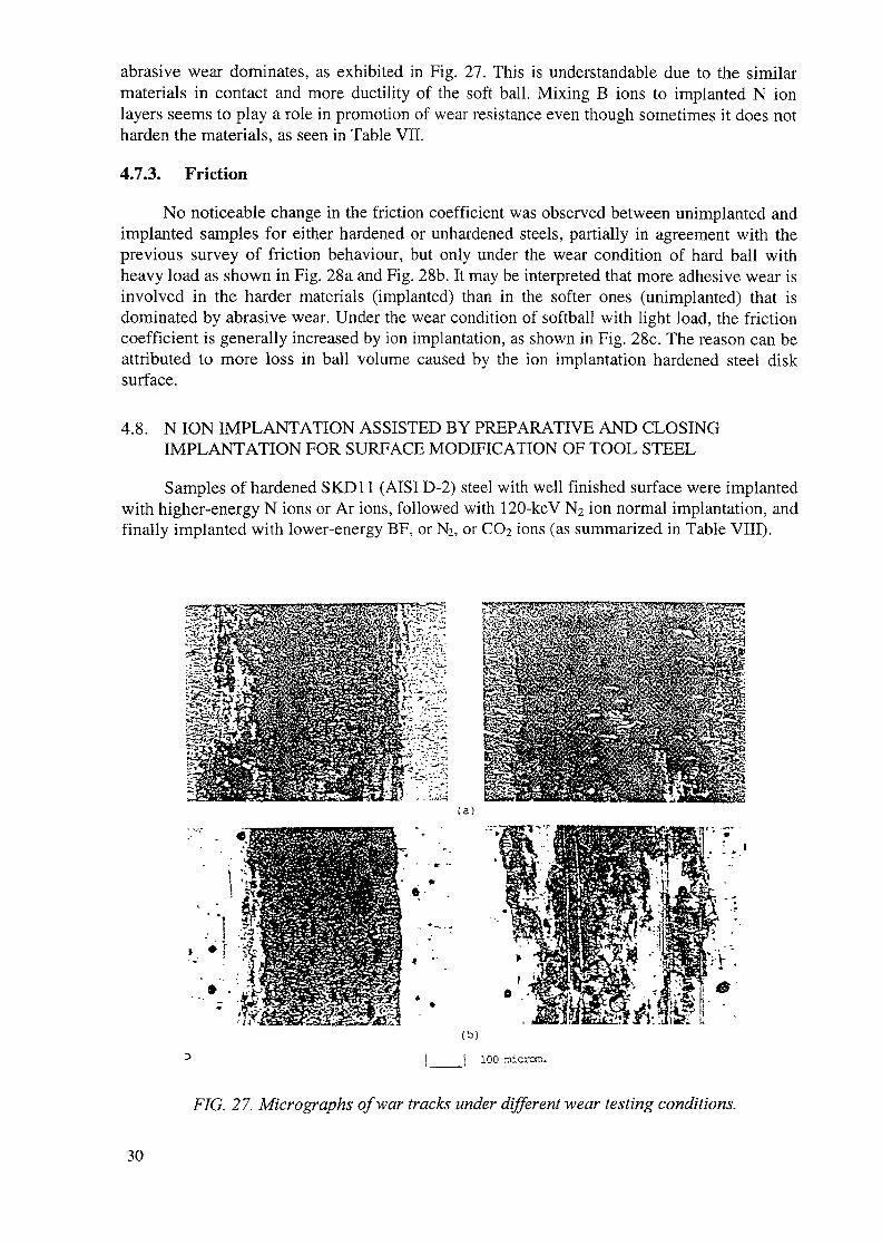
No noticeable change in the friction coefficient was observed between unimplanted andimplanted samples for either hardened or unhardened steels, partially in agreement with theprevious survey of friction behaviour, but only under the wear condition of hard ball withheavy load as shown in Fig. 28a and Fig. 28b. It may be interpreted that more adhesive wear isinvolved in the harder materials (implanted) than in the softer ones (unimplanted) that isdominated by abrasive wear. Under the wear condition of softball with light load, the frictioncoefficient is generally increased by ion implantation, as shown in Fig. 28c. The reason can beattributed to more loss in ball volume caused by the ion implantation hardened steel disksurface.
4.8. N ION IMPLANTATION ASSISTED BY PREPARATIVE AND CLOSINGIMPLANTATION FOR SURFACE MODIFICATION OF TOOL STEEL
Samples of hardened SKD11 (AISID-2) steel with well finished surface were implantedwith higher-energy N ions or Ar ions, followed with 120-keV NI ion normal implantation, andfinally implanted with lower-energy BF, or NZ, or COi ions (as summarized in Table VIII).
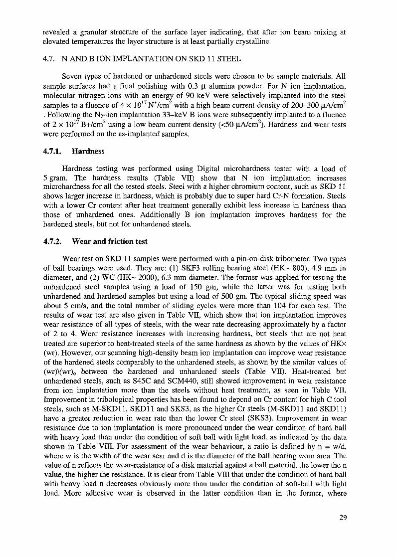
FIG. 27. Micrographs of war tracks under different wear testing conditions.
30
035
__ 030 -
CDjl 025 J
"58 020 -co 015 Mu 010 -
005
O ummplanted,• N-implanted I
0 50 100 150 200 250 300 350Sliding distance (m)
FIG. 28. Friction coefficient of (a) steel: SKS3, unheated, ball: WC, load: 500 gm; steel:SKS3, heated, ball: WC, load: 500 gm; c) steel: SKS3, unheated, ball: WC, load: 150 gm.
4.8.1. Auger electron spectrometry (AES)
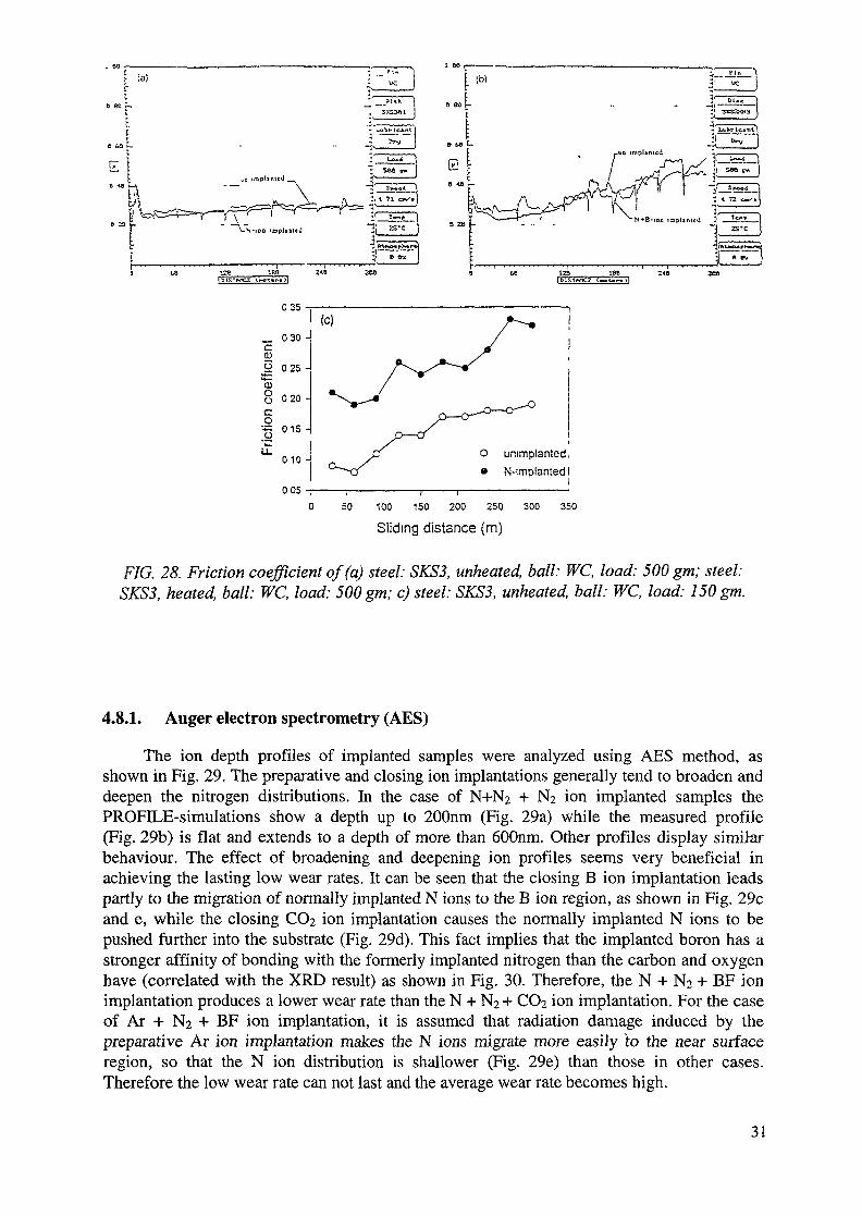
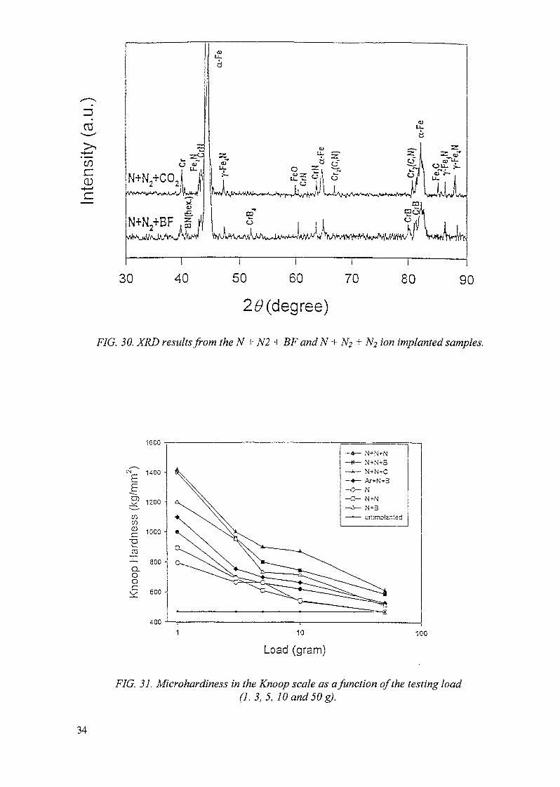
The ion depth profiles of implanted samples were analyzed using AES method, asshown in Fig. 29. The preparative and closing ion implantations generally tend to broaden anddeepen the nitrogen distributions. In the case of N+Na + Na ion implanted samples thePROFILE-simulations show a depth up to 200nm (Fig. 29a) while the measured profile(Fig. 29b) is flat and extends to a depth of more than 600nm. Other profiles display similarbehaviour. The effect of broadening and deepening ion profiles seems very beneficial inachieving the lasting low wear rates. It can be seen that the closing B ion implantation leadspartly to the migration of normally implanted N ions to the B ion region, as shown in Fig. 29cand e, while the closing CC>2 ion implantation causes the normally implanted N ions to bepushed further into the substrate (Fig. 29d). This fact implies that the implanted boron has astronger affinity of bonding with the formerly implanted nitrogen than the carbon and oxygenhave (correlated with the XRD result) as shown in Fig. 30. Therefore, the N + N2 + BF ionimplantation produces a lower wear rate than the N + N2 + CC>2 ion implantation. For the caseof Ar + N2 + BF ion implantation, it is assumed that radiation damage induced by thepreparative Ar ion implantation makes the N ions migrate more easily to the near surfaceregion, so that the N ion distribution is shallower (Fig. 29e) than those in other cases.Therefore the low wear rate can not last and the average wear rate becomes high.
31
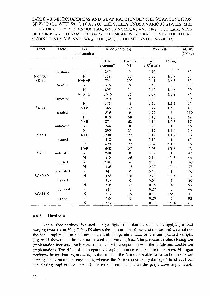
TABLE VII. MICROHARDNESS AND WEAR RATE (UNDER THE WEAR CONDITIONOF WC BALL WITH 500 G LOAD) OF THE STEELS UNDER VARIOUS STATES. AHK= HK - HKo, HK = THE KNOOP HARDNESS NUMBER, AND HKO: THE HARDNESSOF UNIMPLANTED SAMPLES. (WR): THE MEAN WEAR RATE OVER THE TOTALSLIDING DISTANCE, AND (WR)O: THE (WR) OF UNIMPLANTED SAMPLES
Steel
ModifiedSKD11
SKD11
SKS3
S45C
SCM440
SCM415
State
untreated
treated
untreated
treated
untreated
treated
untreated
treated
untreated
treated
untreated
treated
Ionimplantation
-N
N+N+B-
NN+N+B
-N
N+B-N
N+B-
NN+B
-N
N+B-N-N-N-N-N-N
Knoop
HK(Kg/mm2)
266352794676895
1046250371348519818874244295298510620648248312286336341428317356245317459557
hardness
AHK/HK0
(%)032
2000
21550
48390
58680
21220
22270
260170
260120
290
21
Wear rate
wr(10'6mm2)
0.300.180.110.160.100.090.500.200.140.250.100.100.230.170.120.120.090.080.390.140.570.170.470.170.610.150.270.130.200.11
wr/wr0
11/1.71/2.7
11/1.61/1.8
11/2.51/3.6
11/2.51/2.5
11/1.41/1.9
11/1.31/1.5
11/2.8
11/3.4
11/2.8
11/4.1
11/2.1
11/1.8
HKxwr(10-6kg)
806387108909412574491308287565036615652974416357163731935366419261
4.8.2. Hardness
The surface hardness is tested using a digital microhardness tester by applying a loadvarying from 1 g to 50 g. Table IX shows the measured hardness and the derived wear rate ofthe ion implanted samples compared with temperature data of the unimplanted sample.Figure 31 shows the microhardness tested with varying load. The preparative-plus-closing ionimplantation increases the hardness drastically in comparison with the single and double ionimplantations. The effect of the preparative implantation depends on the ion species. Nitrogenperforms better than argon owing to the fact that the N ions are able to cause both radiationdamage and structural strengthening whereas the Ar ions create only damage. The effect fromthe closing implantation seems to be more pronounced than the preparative implantation.
32
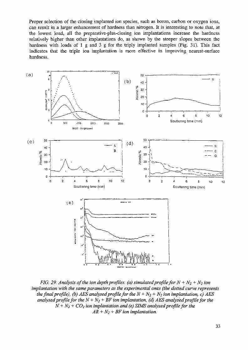
Proper selection of the closing implanted ion species, such as boron, carbon or oxygen ions,can result in a larger enhancement of hardness than nitrogen. It is interesting to note that, atthe lowest load, all the preparative-plus-closing ion implantations increase the hardnessrelatively higher than other implantations do, as shown by the steeper slopes between thehardness with loads of 1 g and 3 g for the triply implanted samples (Fig. 31). This factindicates that the triple ion implantation is more effective in improving nearest-surfacehardness.
(a)
1500 2COO 25CO
4 6 3 10
Scuttenng time (Tin)
(C) (d)
4 6 8 10
Scuttenng time (mm)4 6 s 10Scuttenng time (mm)
12
t e )
FIG. 29. Analysis of the ion depth profiles, (a) simulated profile for N + A^ + A^ ionimplantation with the same parameters as the experimental ones (the dotted curve represents
the final profile), (b) AES analysed profile for the N + fy + N? ion implantation, c) AESanalysed profile for the N + A^ + BF ion implantation, (d) AES analysed profile for the
N + NZ + CO2 ion implantation and (e) SIMS analysed profile for theAR + N2 + BF ion implantation.
33
Inte
nsity
(a.u
.)
Knoo
p H
ardn
ess
(kg/
mm
)o
i I I s-
§
§ S' '
o w Q.
co"
S
CL
CD CO 0) CD
(Jl O CD O
o a *•**.
I <-»* a a. I
O OO O CD O
a-Fe
a-Fe
Fe2C
Ey-
FeN
y-Fe^
N

TABLE VIII. RATIO N BETWEEN THE WEAR SCAR WIDTH AND THE WORN AREADIAMETER OF THE BALL FOR ALL THE UNHEATED STEEL SAMPLES. THE RATIO ISCALCULATED AS A MEAN ONE OVER THE TOTAL SLIDING DISTANCE. HERE, R IS ARATIO BETWEEN N (IMPLANTED) AND N (UNIMPLANTED)
Steel State WC ball, 550g loadn r
SKFSball, ISOgloadn r
M-SKD1 1
SKD11
SKS3
S50C
S45C
SCM440
unimplantedimplanted
unimplantedimplanted
unimplantedimplanted
unimplantedimplanted
unimplantedimplanted
unimplantedimplanted
2.991.463.961.751.601.131.100.761.600.992.741.35
0.49
0.44
0.71
0.69
0.62
0.49
0.620.610.570.510.830.781.000.700.940.690.730.70
0.98
0.89
0.94
0.70
0.73
0.96
4.8.3. Wear test
Wear test of as-implanted samples were performed on pin-on-disk machine usingWC balls with 500g load, 4.8 cm/sliding speed, and 10 000 total-rotations. It can be seen fromthe wear test results (Table DC) that the triple ion implantation generally reduces wearremarkably, while the wear on either the unimplanted sample or the single and the doubleN ion implanted ones is comparatively high. In due succession, the ion species for thepreparative implantation being effective on the wear reduction are nitrogen and argon, and thespecies for the closing implantation are boron, nitrogen, and carbon/oxygen. On the surface ofthe N + N2 + NI and N + N2 + BF ion implanted samples we can observe an extended large-grained or textured structure whereas on the N + N2 + CO2 and Ar + N2 + BF ion implantedsamples we see a much finer and smoother structure. The former microstructure is thought tobe related to nitride or boride formation (as shown in Fig. 30), exhibiting high wear resistance,while the latter is less helpful to wear resistance due to either brittle oxide in the case of the N+ N2 + CO2 ion implanted surface or heavy radiation damage created by Ar ions for the caseof the Ar + N2 + BF ion implanted surface.
TABLE IX. ION IMPLANTATION AND MECHANICAL TESTING RESULTS OF THESKD11 STEEL
Sample
SOSI
S2-1S2-2S3S4S5S6S7
Ion
-N+N2+N2N+N2+BFN+N2+BFN+N2+C02Ar+N2+BF
N2N+N2N2+BF
Energy (keV)
0120-120-90120-120-90120-90-75
120-120-110140-120-90
120120-120120-90
Current(nA/cm2)
0100-200-200100-200-50100-200-30120-120-100200-200-50
200100-200200-95
Dose( 1017/cm2)
02+4+2(N)2+4+2(B)2+4+ 1(B)2+4+2(C)2+4+2(B)
42+4
4+2(B)
HK
470104014101046142011207958951200
Wear rate(10'6mm2)
1.30a
0.110.100.110.140.261.30b
1.26C
0.19
35
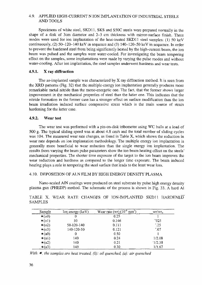
4.9. APPLIED HIGH-CURRENT N ION IMPLANTATION OF INDUSTRIAL STEELSAND TOOLS
Specimens of white steel, SKD11, SKS and S50C steels were prepared normally in theshape of a disk of 3cm diameter and 2-3 cm thickness with mirror-surface finish. Threemodes were used for ion implantation of the heat-treated SKD11 steel samples: (1) 50 keVcontinuously, (2) 50-120-140 keV in sequence and (3) 140-120-50 keV in sequence. In orderto prevent the hardened steel from being significantly heated by the high-current beam, the ionbeam was pulsed and the samples were water-cooled. For investigating the beam temperingeffect on the samples, some implantations were made by varying the pulse modes and withoutwater-cooling. After ion implantation, the steel samples underwent hardness and wear tests.
4.9.1. X ray diffraction
The as-implanted sample was characterized by X ray diffraction method. It is seen fromthe XRD patterns (Fig. 32) that the multiple-energy ion implantation generally produces moreremarkable metal nitride than the mono-energetic one. The fact, that the former shows largerimprovement in the mechanical properties of steel than the latter one. This indicates that thenitride formation in the former case has a stronger effect on surface modification than the ionbeam irradiation induced surface compressive stress which is the main source of strainhardening for the latter case.
4.9.2. Wear test
The wear test was performed with a pin-on-disk tribometer using WC balls at a load of500 g. The typical sliding speed was at about 4.8 cm/s and the total number of sliding cycleswas 104. The measured wear rate changes, as listed in Table X, which shows the reduction inwear rate depends on ion implantation methodology. The multiple energy ion implantation isgenerally more beneficial to wear reduction than the single energy ion implantation. Theresults from varying the beam pulse parameters show the ion beam heating effect on the steels'mechanical properties. The shorter time exposure of the target to the ion beam improves thewear reduction and hardness as compared to the longer time exposure. The beam inducedheating plays a role in tempering the steel surface that leads to the least wear loss.
4.10. DEPOSITION OF ALN FILM BY HIGH ENERGY DENSITY PLASMA
Nano-scaled A1N coatings were produced on steel substrate by pulse high energy densityplasma gun (PHEDP) method. The schematic of the process is shown in Fig. 33. A hard Al
TABLE X. WEAR RATE CHANGES OF ION-IMPLANTED SKD11 HARDENED"SAMPLES
Sample*(oO)*(ol)*(o2)*(o3)*(aO)*(al)*(a2)*(a3)
Ion energy (keV)050
50-120-140140-120-50
0140140140
Wear rate (wr) (10~6 mm2)0.25
0.1460.1110.1210.500.240.210.30
wr/wr0
1"025".25".07
11/2.08
n/2.381/1.67
With *, the samples are heat treated, (0): oil quenched, (a): air quenched
36

alloy was implanted at room temperature with 30 keV nitrogen ions using plasma immersionion implantation (PSII) to a dose of 1.5-6 x 10¹⁷ N+ ion/cm2. This resulted in a uniform,continuous and polycrystalline A1N layer.
oo
' V v ' 50-120-140 kev N-imnLanted
5C kev N-imnlanted
40 .0 5 0 . 0 80 .0i
70. 0
! I I I I I I I I I I2 0 . 0 3 0 . 0 40.0 5 0 . 0 60 .0 7 0 . 0 80 .0 90 .0 100 .0 1 1 0 . 0 1 2 0 . 0
2 7
FIG. 32. XRD patterns of the ion implanted SKD11 samples.
37

FIG 33. Experimental set-up of pulse high energy density plasma coating system.
The as-implanted samples were analyzed by XP§ (Fig. 34) and AES (Fig. 35), whichshows the composite film of AIN, Al, and Al2O3 were produced and thickness of the AINlayer being ~0.15|1. After the coating was made, the as-implanted samples were subjected tocorrosion and microhardness tests. It was observed that the corrosion resistance in the 2% saltwater at room temperature increased by about 10 fold.
4.11. ION IMPLANTATION ON BIO-MATERIALS
It is widely recognized that the wear products of total hip prosthesis pose a significantclinical problem by causing adverse tissue reactions, leading to loosening of the implantfixation, pain, restricted function, and eventually can lead to an expensive and complicatedrevision surgery. In recent years, an increasing amount of research has been focused on thewear behaviour of prostheses and prosthetic joint materials. There are a range of surfacemodification processes, including ion implantation, and coating techniques that are eitherbeing applied on these materials or being evaluated.
XPS spectrums of N Is and Al 2p
405 400 395Binding Energy (eV)
85 80 75 70 65Binding Energ\ (eV)
FIG. 34. XPS spectrum ofN Is andAl 2p on steel substrate.
38
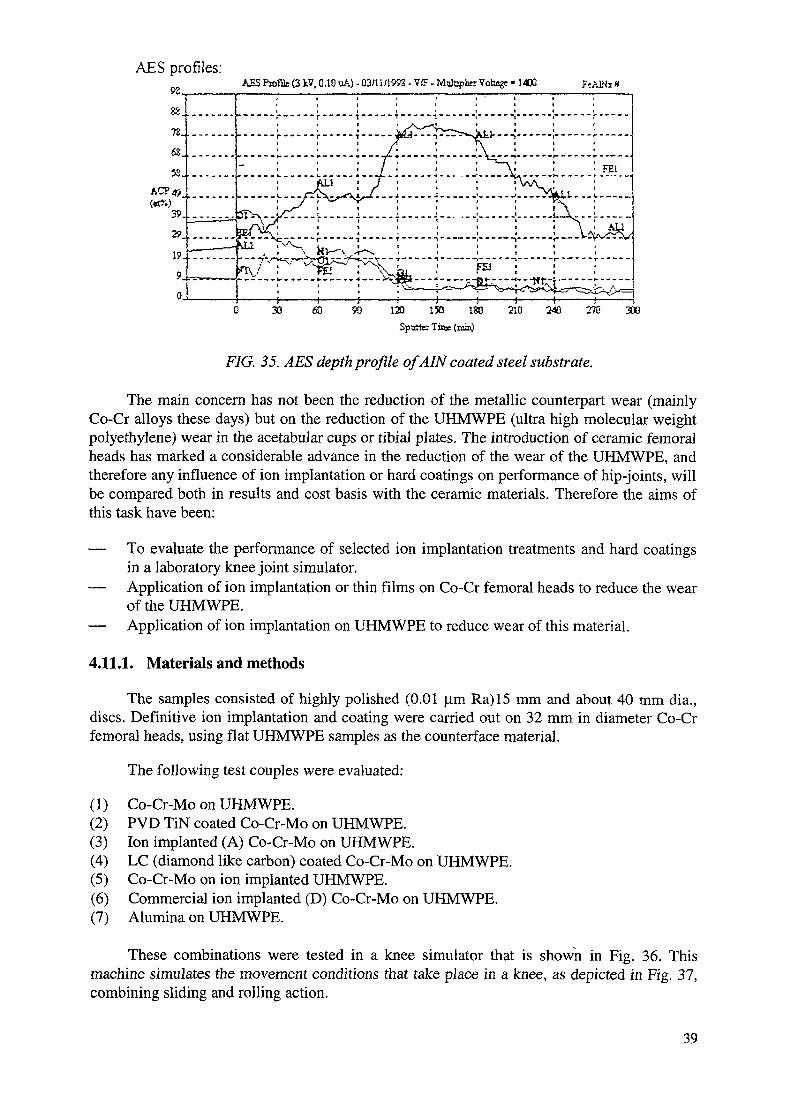
AES profiles:AES Ps>file(3 kV, 0.10 uA) - 03/1U199S - Vff - Mutaphrr Vohags« !400 FcALNi *
30 ffl 90 133 130 180 210 240 270Spatter Time (pr"Q
300
F/G. 35. AES depth profile of AIN coated steel substrate.
The main concern has not been the reduction of the metallic counterpart wear (mainlyCo-Cr alloys these days) but on the reduction of the UHMWPE (ultra high molecular weightpolyethylene) wear in the acetabular cups or tibial plates. The introduction of ceramic femoralheads has marked a considerable advance in the reduction of the wear of the UHMWPE, andtherefore any influence of ion implantation or hard coatings on performance of hip-joints, willbe compared both in results and cost basis with the ceramic materials. Therefore the aims ofthis task have been:
— To evaluate the performance of selected ion implantation treatments and hard coatingsin a laboratory knee joint simulator.
— Application of ion implantation or thin films on Co-Cr femoral heads to reduce the wearof the UHMWPE.
— Application of ion implantation on UHMWPE to reduce wear of this material.
4.11.1. Materials and methods
The samples consisted of highly polished (0.01 u,m Ra)15 mm and about 40 mm dia.,discs. Definitive ion implantation and coating were carried out on 32 mm in diameter Co-Crfemoral heads, using flat UHMWPE samples as the counterface material.
The following test couples were evaluated:
(1) Co-Cr-Mo on UHMWPE.(2) PVD TiN coated Co-Cr-Mo on UHMWPE.(3) Ion implanted (A) Co-Cr-Mo on UHMWPE.(4) LC (diamond like carbon) coated Co-Cr-Mo on UHMWPE.(5) Co-Cr-Mo on ion implanted UHMWPE.(6) Commercial ion implanted (D) Co-Cr-Mo on UHMWPE.(7) Alumina on UHMWPE.
These combinations were tested in a knee simulator that is shown in Fig. 36. Thismachine simulates the movement conditions that take place in a knee, as depicted in Fig. 37,combining sliding and rolling action.
39
FIG. 36. Experimental set-up of knee wear testing machine.
FIG. 37. Movement conditions in a knee and corresponding simulation in thewear testing machine.
4.11.2. Wear test
Wear test was carried out at a load of 500 N, 2 Hz frequency, 12 mm stroke, and5000000 cycles test duration. The characterization of the wear was carried out by UHMWPEweight loss at given cycles, measurement of the UHMWPE wear track volume by using laseroptical profilometry.
4.11.3. Friction test
To complement the knee wear tests, parallel friction tests were also carried out on flatsamples of the same materials and coatings. The friction curves can be seen in Fig. 38. Thetesting conditions are indicated below:
40
8.15
8.12 -
! I I I I I I I I I I I I I I ' I I I I I I I' I I I I I I I I I I I I "I1 I '' I
lELftPSED T1HE (minutes)
FIG. 38. Friction curves of alumina and selected coatings on Co-Cr.
— "Pin/ball-on-disc" tribometer FALEXISC-320 with humidity control.— Ball material: UHMWPE hemispherical pin, 12.6 mm diameter.— Disc Material: Co-Cr untreated and Co-Cr surface treated or coated. Commercial
Alumina.— Surface finish of samples: polished at 0.01 |im Ra.— Applied load: 25 gf. Axial load: 0.2452 N. Nominal contact pressure: 8.61 Mpa.— Lubricant: Bovine serum. Testing temperature: 25°C.— Sliding speed: 50 mm/s. Friction test duration: 60 minutes.
Optical profilometry measurements clearly indicated that there was a combined effect byplastic deformation and wear on the UHMWPE surfaces, therefore masking the results.Hence, the weight loss measurements were more precise in determining the clear effect of thetreatments or coatings on polyethylene wear. For the assessment of wear, the test wasperiodically stopped and the UHMWPE plates were removed for desiccation and weighing.Figure 39 summarizes the weight loss measurements obtained from all material combinations.
The following conclusions can be drawn after these tests:
— The higher UHMWPE weight loss is produced against the TiN coating produced by ionplating (PVD). The surface of this coating clearly shows material transfer frompolyethylene and very small delamination areas can also be observed on theTiN coating. This coating also produces the highest friction coefficient.
— The untreated Co-Cr material produced a weight loss after 5 million cycles of about0.0006 g. On the surface of the ball, there was evidence of significant polyethylenetransfer. With regards to friction behaviour, the coefficient was second worst and agreedwith the wear results.
41
— The best wear results were obtained on DLC coated and ion implanted Co-Cr togetherwith ion implanted UHMWPE, and close to those results obtained for the alumina. Thebest friction coefficient was obtained for the DLC coating.
-0,0006 _
-0,0008 _
-0,001 -
CoCr/UHMWPECoCr+TiN/ UHMWPECoCr+ll(A)/UHMWPECoCr+DLC/ UHMWPECoCr/UHMWPE-HI(B)CoCr+l I (D)/UHMWPEAiumina/UHMWPE
Millones de ciclos
FIG. 39. Weight loss measurements of the UHMWPF material after knee wear tests.
4.12. WEAR FRICTION TEST OF DUAL ION IMPLANTATION AISIM2 STEEL
Three AISIM2 HSS samples, as provided by the supplier were implanted as under:
Sample 1: C+, 20 keV, j = 10 (A/cm2, D = 2 x 10¹⁷ C/cm2.
Sample 2: C+, 20 keV, j = 6 (A/cm2, D = 2 x 10¹⁷ C/cm2 + Zr+, 25 keV, j = 8 (A/cm2, D,18 17= 3 x 10'5 Zr/cmz, D(retained) = 2 x 10" Zr/cm .
Sample 3: C+, 20 keV, j = 10 (A/cm2, D = 2 x 10¹⁷C/cm2 + Ta+, 20 keV, j = 4 (A/cm2,D=1.5xl017Ta/cm2.
Three implanted AISIM2 steels were tested in a ball-on-disk FALEX machine ISC 320with humidity control cabinet. For each sample two loads were applied: 25 and 250 gf. Thegeneral conditions of the tests are shown in Table XI. Friction results for all samples and thesubstrate material at 25 and 250 gf are presented in Figs. 40 and 41. These curves, clearlyshow that combined implantation of C and Zr ions leads to a significant friction reduction atthe 2 loads investigated. The samples had a distinct colour change after ion implantation. Noattempt was made in our laboratory to investigate on the nature and composition of theoutermost layers.
42
1 68
8.88 -
8.28
3880 .______i NUMBER OF TURNS]
FIG 40 Friction curves ofunimplanted and implanted AISI M2 high speed steel at a loadof25gf.
1 B8
8.28 -
I I ! 1 | I I I I I I I I I | I I I ' j———, I I | I I—— | I I I I | I I I I | 1 I I———
688 1208.______1888. 2488. 3888.I NUMBER OF TUKHS]
FIG 41 Friction curves ofunimplanted and implanted AISI M2 high speed steel at a loadof250gf
43

TABLE XL EXPERIMENTAL CONDITIONS OF WEAR TEST
Ball materialBall diameter (mm)
Disc material
Load (g)Speed (rpm)
Temperature (C)Relative humidity (%)
Track radius (mm)Lubricant
Lower load52100 steel
10.0AISI M2 high speed steel
25502560
15.0none
Higher load52100 steel
10.0AISI M2 high speed
steel250502560
12.5none
4.13. PRELIMINARY ION IRRADIATION OF SUBSTRATE FOR IMPROVEMENT OFCOATING MECHANICAL PROPERTIES
Argon ion implantation was performed on carbon steel of Y8A type (at.%: 0.22 Mn,0.16 Cr, 3.58 C, 0.48 Si; Hv = 4.3 GPa) samples by ion beam accelerator of ELY-4 model. Thesamples were implanted with an ion current density of 2 |iA/cm2 and the ion doses rangedfrom 1 x 10¹⁷ to 1 x 10¹⁷ ions/cm2. Vacuum level of the chamber was set tolxlO"3 Pa and theimplantation energy of Ar+ ion was 30 keV. After Ar+ ion irradiation TiN coating made by acathodic arc plasma deposition (CAPD) technique (= 100A, pN = 1x10^ Pa, Usub = 120 V,Tsub = 20°C and 300°C, coating thickness h = 1 um).
4.13.1. Auger electron spectrometry (AES)
The as-deposited samples were characterized by Auger electron spectrometry (AES)using Auger spectrometer PHI-660 (Perkin Elmer).
4.13.2. Scratch and adhesion test
The adhesion of the deposited layer was measured by using a VTT Tech Scratch Testerequipment at a load 100 N/min. Rockwell diamond indenter was used as a counter sample.The speed of translation was set to 10 mm/min.
4.13.3. Friction test
Friction coefficient of as-deposited samples were carried out in a TAY-1MY tribometerat a load of 0.7 N.
4.13.4. Mechanical properties of TiN coatings
It is clear that the best adhesion is observed for coating deposited ~on the irradiatedsubstrate (up to a dose of 1 x 10¹⁷ Ar+/cm2) and for coating deposited on the substrate heatedup to 300°C. The use of preliminary irradiation leads to decrease of friction coefficient by 20-30% for TiN coatings (Table XII). The use of Ar+ ion implantation of the steel substratebefore TiN coating deposition improves significantly its adhesion and friction properties.
44
TABLE XII. SUBSTRATE TREATMENT MODE
Substratetemperature (C)
20
300
Substrate irradiation dose,(1016 Ar+/cm2)
015100
Critical loadUN5.66.6
—11.310.8
FrictionCoefficient
0.430.350.330.330.49
4.14. DEPOSITION OF TIN LAYER BY PLASMA GUN
4.14.1. Impulse plasma deposition method (IPD)
Titanium nitride coating on speed steel SW7M was carried out by IPD method. Impulseplasma deposition method based on utilization of coaxial impulse plasma accelerator asplasma source in the synthesis of coating materials. The coaxial impulse plasma acceleratorconsists of high current generator and two axial electrodes, separated at one end by insulator,placed inside the discharge chamber. Working gas (nitrogen) at uniform density andtemperature fill the space between electrodes, of which the internal one is anode. When thecapacitor bank in the current generator is discharged through the gas, an axially symmetriccurrent sheet forms at the surface of insulator and driven by Lorentz force, propagates axiallyalong the electrodes to their opened end. This leads to massive erosion of the electrodematerial, here Ti, and creates nitrogen-titanium plasma.
4.14.2. Deposition of TiN by means of PVD type steered arc evaporation (St-Arc)
Deposition of TiN layer on SW7M steel was carried out by means of PVD type steeredarc evaporation as well as combination of (St-Arc) and DPE method. The device wasequipped with titanium cathode of 40 mm diameter and ceramic insulator, both in cylindricalgeometry. The arc stabilization has been provided by an axial magnetic field of several oerstedintensity. The arc has been ignited by mechanical opening of the special element of theelectrical circuit. The discharge current was maintained on the level of 60A in order toeliminate creation of multidrops effect. The deposition procedure has been carried out in oneexperimental chamber, without stopping of the process and exposing samples to theatmospheric air. During deposition the target material was heated up to 500 C.
Characterization of the samples have been carried out using the following methods:
— Measurements of Ti distribution on the specimen surface by means of electronmicroprobe microhardness measurements HV001 and HV at different load (20-100G).
— Roughness measurements.— Microscope study of the sample surface.— Relative thickness of Ti interlayer estimation by means of X ray analysis.
Characterization of the different type TiN coating is presented on Table XIH. All typesof TiN coatings obtained from this experiment were of very good adhesion and extremelyhigh hardness.
45
4.14.2.1. Adhesion test
Adhesion test was performed by using an advance CSEM REVETEST device, equippedwith diamond indenter ROCKWELL, ball type with diameter of r = 200 |0,m and forcomparison — by means of indentation method HRC with evaluation of the indenter tracesaccording scale HF1-HF6.
4.14.2.2. Weariest
The wear test of TiN coated samples have been performed by means of DUCOMtrybotester TM-28M equipped with ball r = 3 mm operating in ball-on-plain mode at slidingreversible motion. Wear tests have been performed on the two selected samples:
Sample a: TiN coating deposition on the SW7M steel substrate by means of Steered ArcEvaporation technology combined with HIPIB-DPE processing (Table Xffl, sampleno. 117).Sample b: TiN coating deposition on the SW7M steel substrate by means of EPD methodcombined with HIPIB-DPE processing (Table XIII, sample no. 140).
As reference material speed steel SW7M substrate has been used. Each of the sampleshas been subject to a series of 5 measurements with different number of cycles and differenttime duration of the tests (1-20 min.). The applied load was the same (5N) for allmeasurements, except measurement number of jklb for sample b. Only in this case the
TABLE XIII. CHARACTERIZATION OF TIN COATINGS
No.
1103
119
118
117
137
138
139
140
141
143
Process
2Ti + TiN(Arc)
T=400°CTi(DPE-lSOns)
TiN(Arc)T=400°C
Ti(DPE- 190ns)TiN(Arc)T=400°C
Ti(DPE-200ns)TiN(Arc)T=400°CTiN(IPD)T=400°C
Ti(DPE- 180ns)TiN(IPD)T=400°C
Ti(DPE- 190ns)TiN(IPD)T=400°C
Ti(DPE-200ns)TiN(IPD)T=400°C
Ti(DPE- 180ns)TiN(IPD)
Without heatingTiN(IPD)
Without heating
DepositionTiN [nm/s]
34,5
4.0
4.5
4.0
4.8
4.2x1 04
6.0x10"
7.0x1 04
7.0x10"
6,8x1 04
ThicknessTiN [nm]
42,7
2,4
2,7
2,4
2,9
2,1
3,4
2,9
3,5
3,4
RoughnessRa [nm]
50,26
0,39
0,36
0,39
0,41
0,85
1,08
0,62
0,32
0,33
Orientation/f-texture
factor/6
(111)70,38
(1 1 1)/0,83
(111)70,78
(111)70,83
(111)70,75
(200)7-0,024
(200)7-0,32
(200)7-0,386
(111)70,67
(111)70,82
Interlayerdistance [A]
74.240
4,246
4,240
4,246
4,220
4,212
4,215
4,216
4,204
4,206
AdhesionHF[l-6]
8HF5
HF1
HF1
HF1
HF1
HF2
HF1
HF1
HF1
HF1
AdhesionLc[N]
921
53
51
53
—0
29
20
27
12
16
46

applied load has been changed to ION. The detailed description of the experimental conditionsare presented in Table XIV.
TABLE XIV. EXPERIMENTAL CONDITIONS FOR THE WEAR RESISTANCE TESTSOF TIN COATINGS
Sample a:
MeasurementNumber
JklaJk2aJk3aJk4a
Load Fn
5N5N5N5N
Number of cycles/sec(here and back)
1115
Measurement durationtime5 min10 min20 min20 min
Number ofcycles
300600
12006000
Sample b:
Measurement Load Fn Number of cycles/secNumber_____________(here and back)
Measurement durationtime
Number ofcycles
(*)JklbJk2bJk3b
(**)Jk4b
5N5N5N
ION, 5N
5555
Imin1 min
20 min20 min
30030
60006000
(*) - trace out of the area(**)- the load has been decreased during the test
The "experimental results" are presented in Table XV. Maximal values are calculatedseparately for the sliding "ball-on-plane" in two directions, to right and to left (here and back).Lack of the symmetry could be caused by the "construction of the device" (systematic error)and could be eliminated by calculation of the average value of the Friction Force Ftav
= (Fimax +F2max)/2.
TABLE XV. EXPERIMENTAL RESULTS
Sample a:
MeasurementJklaJk2aJk3aJk4a
i'l.max2.40N2.75N2.85N3.30N
F2,max3.60N4.30N4.00N4.75N
•Tav.3.00N3.52N3.42N4.02N
H = Fav. /Fn0.600.700.680.80
Sample b:
MeasurementJklbJk2bJk3bJk4b
Flmax3.80N3.00N4.50N4.00N
8.05N (*)
•T2,max4.20N3.00N4.30N4. ION
8.80N (*)
Fav.4.00N3.00N4.40N4.05N
8.42N (*)
M-= Fav. /Fn
0.800.600.880.81
0.84 (*)(*)-loadFn = ION
47
The TiN coating produced with use of combination of St-Arc method as well as the IPDis characterized by extremely high wear-resistance caused probably by their very highhardness and adhesion. The only disadvantage of these techniques is relatively high roughnessof the coating surface.
4.15. FORMATION OF TIN LAYER ON HSS PROFILE MILLING CUTTERS ANDSTEEL BALL VALVES
4.15.1. Deposition of tin layer on HSS profile milling cutters
TiN coating on HSS profile milling cutters was carried out by both the magnetronsputtering deposition and pulsed high voltage discharge ion implantation. The schematic ofthis process is shown in Fig. 42. The experiments have been carried out using an equipment
. Magnetron Shields 5.
FIG. 42. Experimental set-up for combined magnetron sputtering deposition and ionimplantation treatment.
48
especially designed and built for combined treatments of plasma nitriding, magnetronsputtering and ion implantation (Fig. 42). The treatment chamber (1), has cylindrical shapewith water cooled walls. The inner diameter is 300 mm and the height is 425 mm. On thebottom plate a circular magnetron (2) with an active target area of -40 cm2 is mounted. Theanode of magnetron (3) is a stainless steel ring with a diameter of 165 mm, 2 mm thicknessand 15 mm width. It is positioned at 220 mm above the bottom plate, insulated from thechamber wall. A pair of shields (5) cover the magnetron target surface when a plasmanitriding treatment is performed. On the bottom, plate four ceramic columns (6) are alsomounted which hold the kanthal heaters. These are used to heat the workpiece before sputtercleaning. The workpiece is suspended by a special device (7), which is supported by a ceramicinsulator (8), tested up to 150 kV. This entire mechanical structure is positioned on the topplate. A spherical shield (9) prevents the sputtering deposition on the inner surface of theceramic insulator.
The gases, argon, nitrogen, hydrogen, are introduced into the treatment chamber bymeans of calibrated needle valves. A 500 1/s diffusion pump is used for the evacuation of thechamber. When a plasma nitriding treatment is performed, the diffusion pump is shut off andonly the rotary pump is used. The discharge and the components subjected to the treatmentcan be visually inspected through the window (10) located opposite to the vacuum port. TheX ray produced during the high voltage pulsed discharge are significantly attenuated by thechamber walls except in the window region, where a special shield has been introduced toprotect this area also. The main operational parameters of this experimental set up are listed inTable XVI.
Process optimization and the building of pilot scale coating installation forwear/corrosion investigations of ball valves used in oil extraction pumps by ion beam assisteddeposition of Ti(Al)N.
TABLE XVI. EXPERIMENTAL PARAMETERS
Parameter Without High Voltage With High VoltagePartial pressure of N2Partial pressure of Ar
Magnetron current intensityBias voltage
High voltage amplitudeCurrent intensity of the high voltage
dischargeCharacteristics
HardnessThicknessAdherence
Structure, constitution
1.6xl(Ttorr1.8 A
70-90 V
2700-2900 HV0.04(2.7±0.2) JimLc = 30-35 N
Preferential orientationTJN(lliyri2N(200)
1.6x 10'3torr1.8 A
60-120 V40 kV4-5 A
2300-2500 HV0.04(2.6+0.2) |4,mLc = 25-30 N
Preferential orientationTiN(lll)/Ti2N(200)
TiN thin films were deposited by magnetron sputtering of titanium targets in a mixtureof argon and nitrogen at a pressure of 5 x 10~3 mbar. The deposition chamber is provided withthree rectangular magnetrons. During growth, the deposited thin films were assisted with anintense ion flux drawn from the surrounding plasma by the negatively biased substrates.
49
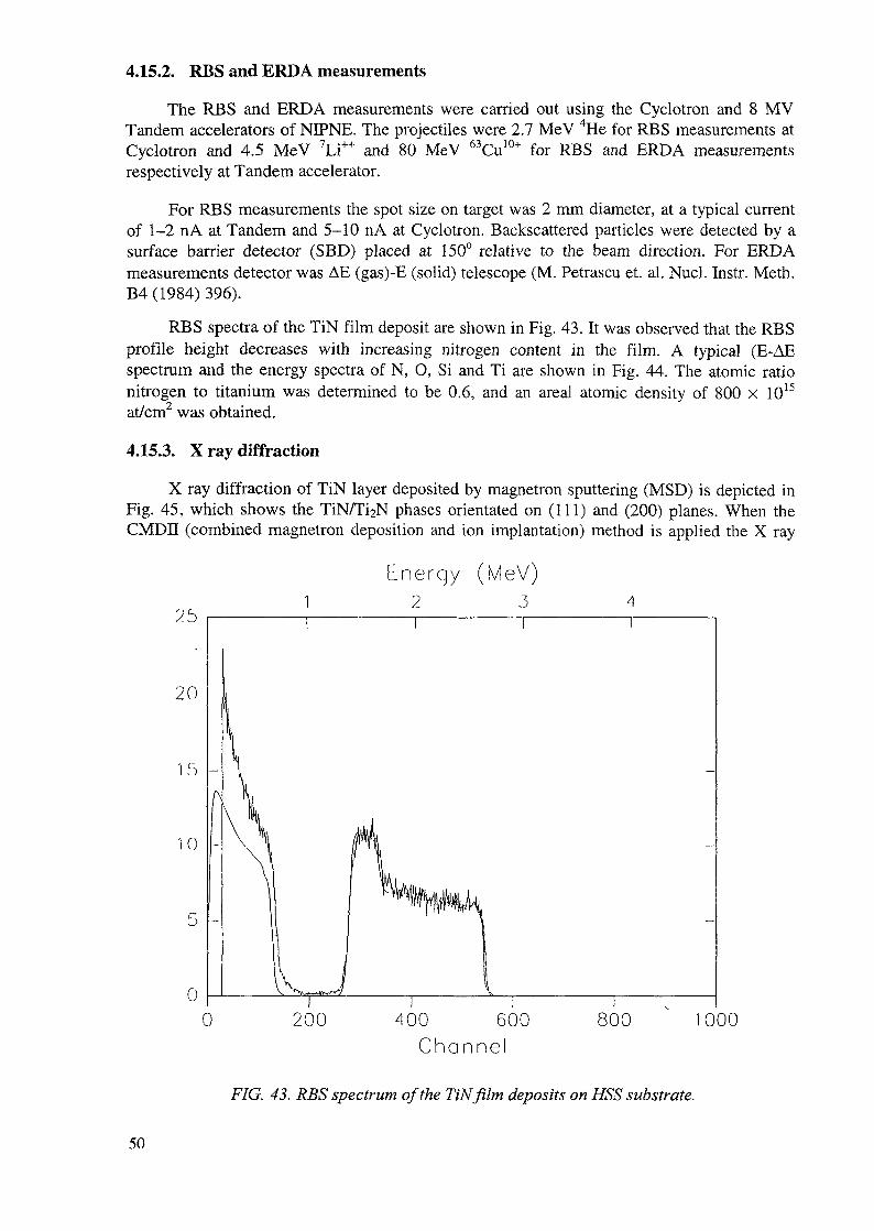
4.15.2. RBS and ERDA measurements
The RBS and ERDA measurements were carried out using the Cyclotron and 8 MVTandem accelerators of NIPNE. The projectiles were 2.7 MeV 4He for RBS measurements atCyclotron and 4.5 MeV 7Li++ and 80 MeV 63Cu10+ for RBS and ERDA measurementsrespectively at Tandem accelerator.
For RBS measurements the spot size on target was 2 mm diameter, at a typical currentof 1-2 nA at Tandem and 5-10 nA at Cyclotron. Backscattered particles were detected by asurface barrier detector (SBD) placed at 150° relative to the beam direction. For ERDAmeasurements detector was AE (gas)-E (solid) telescope (M. Petrascu et. al. Nucl. Instr. Meth.B4( 1984) 396).
RBS spectra of the TiN film deposit are shown in Fig. 43. It was observed that the RBSprofile height decreases with increasing nitrogen content in the film. A typical (F-AF.spectrum and the energy spectra of N, O, Si and Ti are shown in Fig. 44. The atomic rationitrogen to titanium was determined to be 0.6, and an areal atomic density of 800 x 1015
at/cm2 was obtained.
4.15.3. X ray diffraction
X ray diffraction of TiN layer deposited by magnetron sputtering (MSD) is depicted inFig. 45, which shows the TiN/Ti2N phases orientated on (111) and (200) planes. When theCMDn (combined magnetron deposition and ion implantation) method is applied the X ray
linerqy (MeV)1 2 3
200 400 600Channel
800 1000
FIG. 43. RBS spectrum of the TiN film deposits on HSS substrate.
50
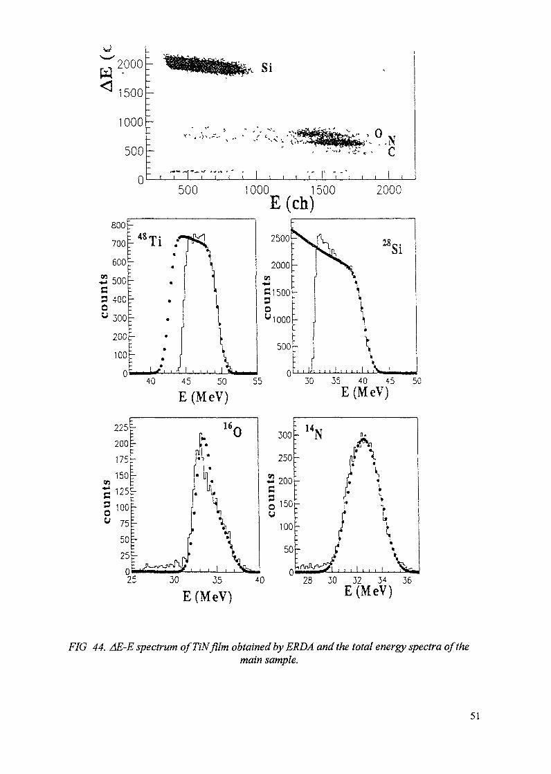
2000 -15001000500
0500 1000 1500
E(ch)2000
E(MeV)
225
200r r
160E-c
I75irP
en [f*J 1 7<;C-
5 100^-ou 75
50
25
-
-
[HI.•iI -1-"1« L»
• *1
•1
r f ^r rJ" V
300
250
•2 200C
§ 150u
100
50
ft
-"N
! f0 ——— ——— —————————— — y. ——— • ———25 30 35 *0 28 30
E(MeV)
Pn
JoVl„[' ^F 1i ir \
f '• vr '
"vr
. . . . . . , v32 34 36
E (MeV)
F/G 44. AE-E spectrum of TIN film obtained by ERDA and the total energy spectra of themain sample.
51
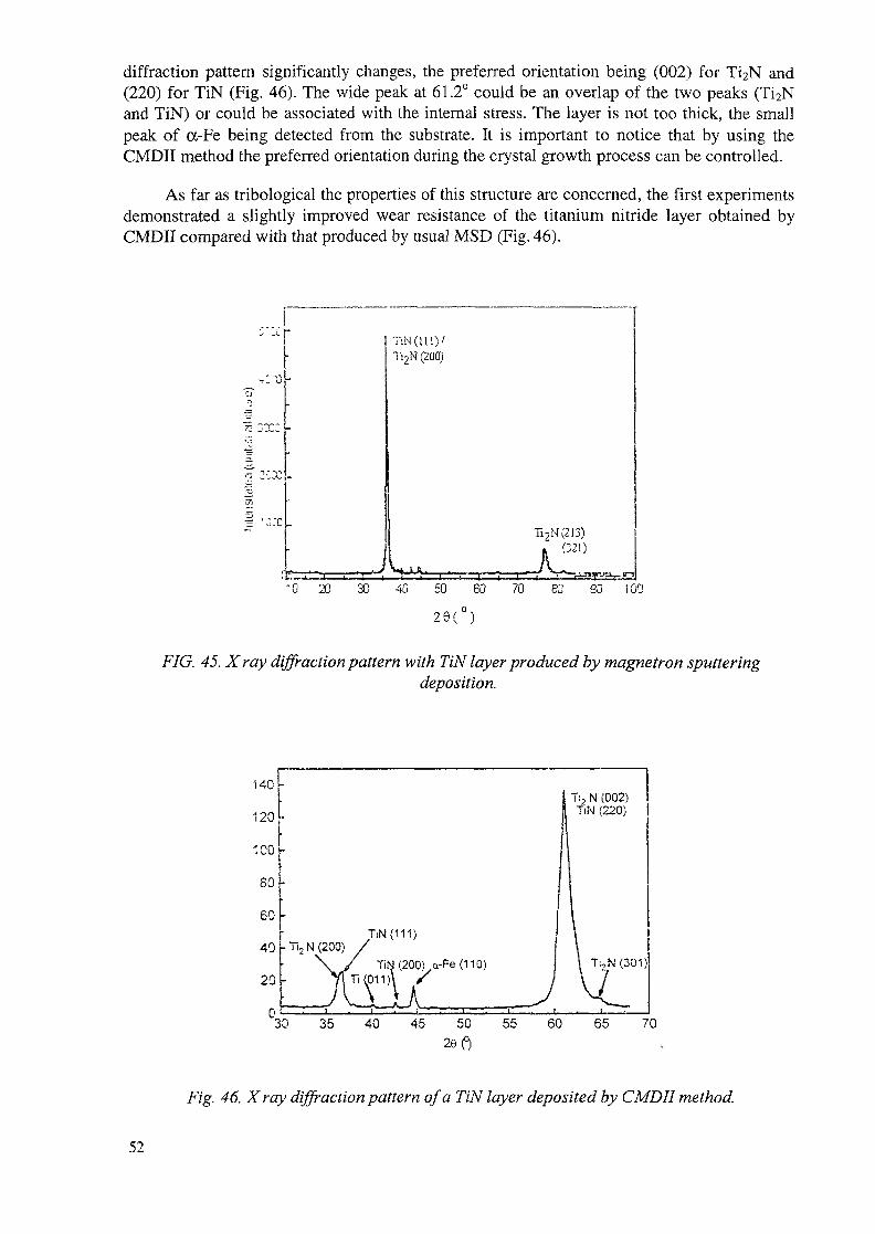
diffraction pattern significantly changes, the preferred orientation being (002) for TiaN and(220) for TiN (Fig. 46). The wide peak at 61.2° could be an overlap of the two peaks (Ti2Nand TiN) or could be associated with the internal stress. The layer is not too thick, the smallpeak of a-Fe being detected from the substrate. It is important to notice that by using theCMDII method the preferred orientation during the crystal growth process can be controlled.
As far as tribological the properties of this structure are concerned, the first experimentsdemonstrated a slightly improved wear resistance of the titanium nitride layer obtained byCMDII compared with that produced by usual MSD (Fig. 46).
Ti2N (200)
Ti2N(2I3)(321)
'0 20 3] 40 50 60 70 80 100
FIG. 45. Xray diffraction pattern -with TiN layer produced by magnetron sputteringdeposition.
140
120
ICO
SO
60
40
20
'•
.TIN (111)
- Ti2 N (200) /\_y TIN (200) a-Fe (110)
T;2 N (002)TiN (220)
\ T.2N(301)
• K^\( J \LQ —————————————————————————————————————on or- XA AC cr\ ccr &r\ cc ~?30 35 40 45 50 55
26060 65 70
Fig. 46. Xray diffraction pattern of a TiN layer deposited by CMDII method.
52
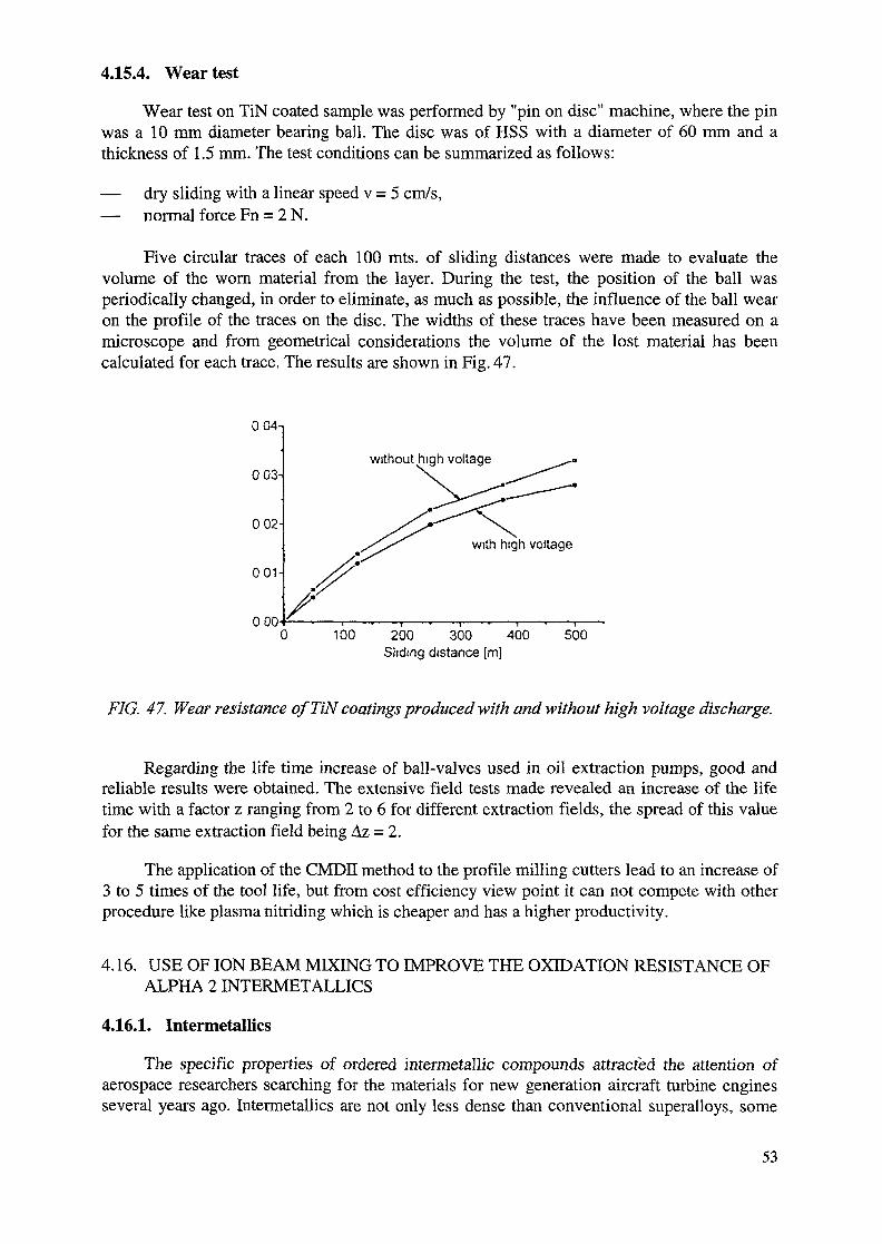
4.15.4. Weariest
Wear test on TiN coated sample was performed by "pin on disc" machine, where the pinwas a 10 mm diameter bearing ball. The disc was of HSS with a diameter of 60 mm and athickness of 1.5 mm. The test conditions can be summarized as follows:
— dry sliding with a linear speed v = 5 cm/s,— normal force Fn = 2 N.
Five circular traces of each 100 mts. of sliding distances were made to evaluate thevolume of the worn material from the layer. During the test, the position of the ball wasperiodically changed, in order to eliminate, as much as possible, the influence of the ball wearon the profile of the traces on the disc. The widths of these traces have been measured on amicroscope and from geometrical considerations the volume of the lost material has beencalculated for each trace. The results are shown in Fig. 47.
004-!
003-
002-
001-
000
without high voltage
with high voltage
0 100 200 300 400 500Sliding distance [m]
FIG. 47. Wear resistance of TiN coatings produced with and without high voltage discharge.
Regarding the life time increase of ball-valves used in oil extraction pumps, good andreliable results were obtained. The extensive field tests made revealed an increase of the lifetime with a factor z ranging from 2 to 6 for different extraction fields, the spread of this valuefor the same extraction field being Az = 2.
The application of the CMDII method to the profile milling cutters lead to an increase of3 to 5 times of the tool life, but from cost efficiency view point it can not compete with otherprocedure like plasma nitriding which is cheaper and has a higher productivity.
4.16. USE OF ION BEAM MIXING TO IMPROVE THE OXIDATION RESISTANCE OFALPHA 2 INTERMETALLICS
4.16.1. Intermetallics
The specific properties of ordered intermetallic compounds attracted the attention ofaerospace researchers searching for the materials for new generation aircraft turbine enginesseveral years ago. Intermetallics are not only less dense than conventional superalloys, some
53
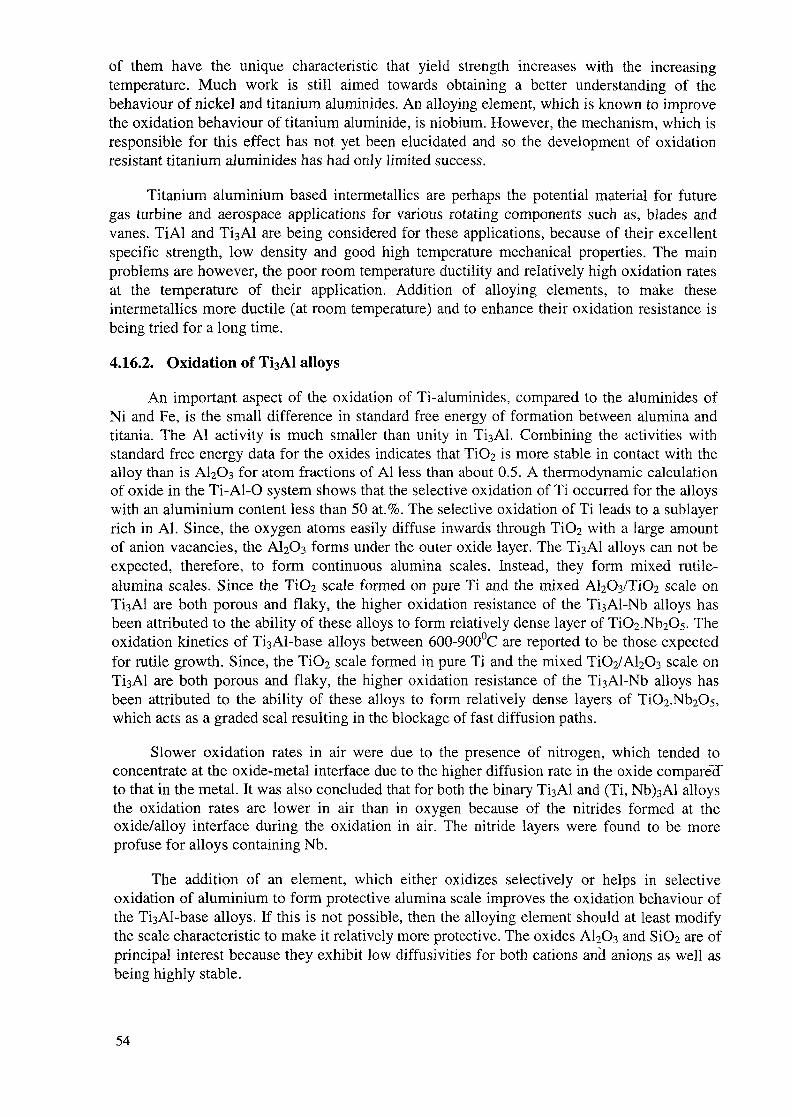
of them have the unique characteristic that yield strength increases with the increasingtemperature. Much work is still aimed towards obtaining a better understanding of thebehaviour of nickel and titanium aluminides. An alloying element, which is known to improvethe oxidation behaviour of titanium aluminide, is niobium. However, the mechanism, which isresponsible for this effect has not yet been elucidated and so the development of oxidationresistant titanium aluminides has had only limited success.
Titanium aluminium based intermetallics are perhaps the potential material for futuregas turbine and aerospace applications for various rotating components such as, blades andvanes. TiAl and Ti3Al are being considered for these applications, because of their excellentspecific strength, low density and good high temperature mechanical properties. The mainproblems are however, the poor room temperature ductility and relatively high oxidation ratesat the temperature of their application. Addition of alloying elements, to make theseintermetallics more ductile (at room temperature) and to enhance their oxidation resistance isbeing tried for a long time.
4.16.2. Oxidation of Ti3Al alloys
An important aspect of the oxidation of Ti-aluminides, compared to the aluminides ofNi and Fe, is the small difference in standard free energy of formation between alumina andtitania. The Al activity is much smaller than unity in TiaAl. Combining the activities withstandard free energy data for the oxides indicates that TiOa is more stable in contact with thealloy than is A^Os for atom fractions of Al less than about 0.5. A thermodynamic calculationof oxide in the Ti-Al-O system shows that the selective oxidation of Ti occurred for the alloyswith an aluminium content less than 50 at.%. The selective oxidation of Ti leads to a sublayerrich in Al. Since, the oxygen atoms easily diffuse inwards through TiOa with a large amountof anion vacancies, the AliOa forms under the outer oxide layer. The Ti3Al alloys can not beexpected, therefore, to form continuous alumina scales. Instead, they form mixed rutile-alumina scales. Since the TiOi scale formed on pure Ti and the mixed AlaOs/TiOi scale onTi3Al are both porous and flaky, the higher oxidation resistance of the Ti3Al-Nb alloys hasbeen attributed to the ability of these alloys to form relatively dense layer of TiO2.Nb2C>5. Theoxidation kinetics of Ti3Al-base alloys between 600-900°C are reported to be those expectedfor rutile growth. Since, the TiO2 scale formed in pure Ti and the mixed TiO2/Al2O3 scale onTi3Al are both porous and flaky, the higher oxidation resistance of the Ti3Al-Nb alloys hasbeen attributed to the ability of these alloys to form relatively dense layers of TiOa.NbiOs,which acts as a graded seal resulting in the blockage of fast diffusion paths.
Slower oxidation rates in air were due to the presence of nitrogen, which tended toconcentrate at the oxide-metal interface due to the higher diffusion rate in the oxide compared"to that in the metal. It was also concluded that for both the binary Ti3Al and (Ti, Nb)3Al alloysthe oxidation rates are lower in air than in oxygen because of the nitrides formed at theoxide/alloy interface during the oxidation in air. The nitride layers were found to be moreprofuse for alloys containing Nb.
The addition of an element, which either oxidizes selectively or helps in selectiveoxidation of aluminium to form protective alumina scale improves the oxidation behaviour ofthe Ti3Al-base alloys. If this is not possible, then the alloying element should at least modifythe scale characteristic to make it relatively more protective. The oxides AlaOs and SiOi are ofprincipal interest because they exhibit low diffusivities for both cations and anions as well asbeing highly stable.
54

The addition of Nb to TisAl slows the rate of high temperature oxidation as the result ofdoping of the TiOa in the scale. The dissolution of Nb+5 into TiO2 is expected to reduce theconcentration of both Ti-interstitial and O-vacancies. Although the high temperature of theternary Nb modified TijAl alloys offer attractive high temperature mechanical properties, theoxidation resistance of these alloys are not satisfactory for their high temperature uses.
In this work, the surface modification of the TisAl-Nb alloys have been tried by:Cr nitrided by plasma arc, plasma nitriding and Al/Ar + ion beam mixing. Three differentTiaAl-Nb alloys of following compositions were used in this work: Ti-25Al-llNb, TJ-24A1-20Nb and Ti-22Al-20Nb.
4.16.3. Ion beam mixing
A coating of aluminium was made by deposition of Al using PVD. This was followedby implantation of a 30 keV Ar+ ion beam. Ion implantation facility of the University ofBombay, was used for this purpose. The samples were coated with 300A Al thin film fromboth sides at room temperature (by PVD method), followed by the implantation with Ar+ ionat an operating voltage of 30 keV for a total of 1 x 10¹⁷ ions/cm2. Average beam current wasmaintained at 8.5^iA. Vacuum during implantation was of the order of 7 x 10~5 torr.
4.16.4. Plasma nitriding
Plasma nitriding was carried out at Multiarc Pune. The pressure of nitrogen wasmaintained at 0.4 torr. with a ratio of N2:H2 = 1:3. The temperature used for coating was750°C and the coating took about 2 h
Oxidation tests were carried out in air at 800°C. The weight change of the sample wasrecorded continuously during the oxidation. The oxide scale was characterized using opticalmicroscope, XRD and SEM/EDAX.
4.16.5. Plasma - Arc CrN coating
Scanning electron micrographs of chromium nitrided Ti-25Al-llNb, Ti-24Al-20Nballoys before oxidation are shown in Fig. 48. Unmelted chromium is seen in the form ofbubbles on the surface of the alloys. Distribution of various elements present in the coating isshown in the X ray area scan maps depicted in Fig. 49, which shows a weak but uniformdistribution of nitrogen and densely distributed chromium in the coating. X ray diffractionanalysis (Fig. 50) reveals the presence of chromium nitride (CrN) as the main phase in thecoating. Surface composition for CrN layers on Ti-25Al-l 1Mb and Ti-24Al-20Nb sample wasdetermined by ED AX as shown in Tables XVII and XVIII.
These analyses confirm that the coating consists mainly of CrN with some incorporationof Ti and Nb. Small traces of Al were also found in the coating.
4.16.6. Plasma nitriding coating
Scanning electron micrograph of plasma nitrided Ti-25Al-llNb alloys before oxidationis shown in Fig. 51. Some local inhomogenities can be seen on the coated surface.Distribution of various elements present in the coating is shown by the X ray area scan mapsdepicted in Fig. 52, which reveal a weak but uniform distribution of nitrogen and densedistribution of Ti, Nb, and Al in the coating. X ray analysis (Fig. 53) reveals the presence oftitanium nitride (TiN) as the main phase in the coating. Surface composition for TIN layer onthe coating was determined using ED AX. The results are given in Table IXX.
55
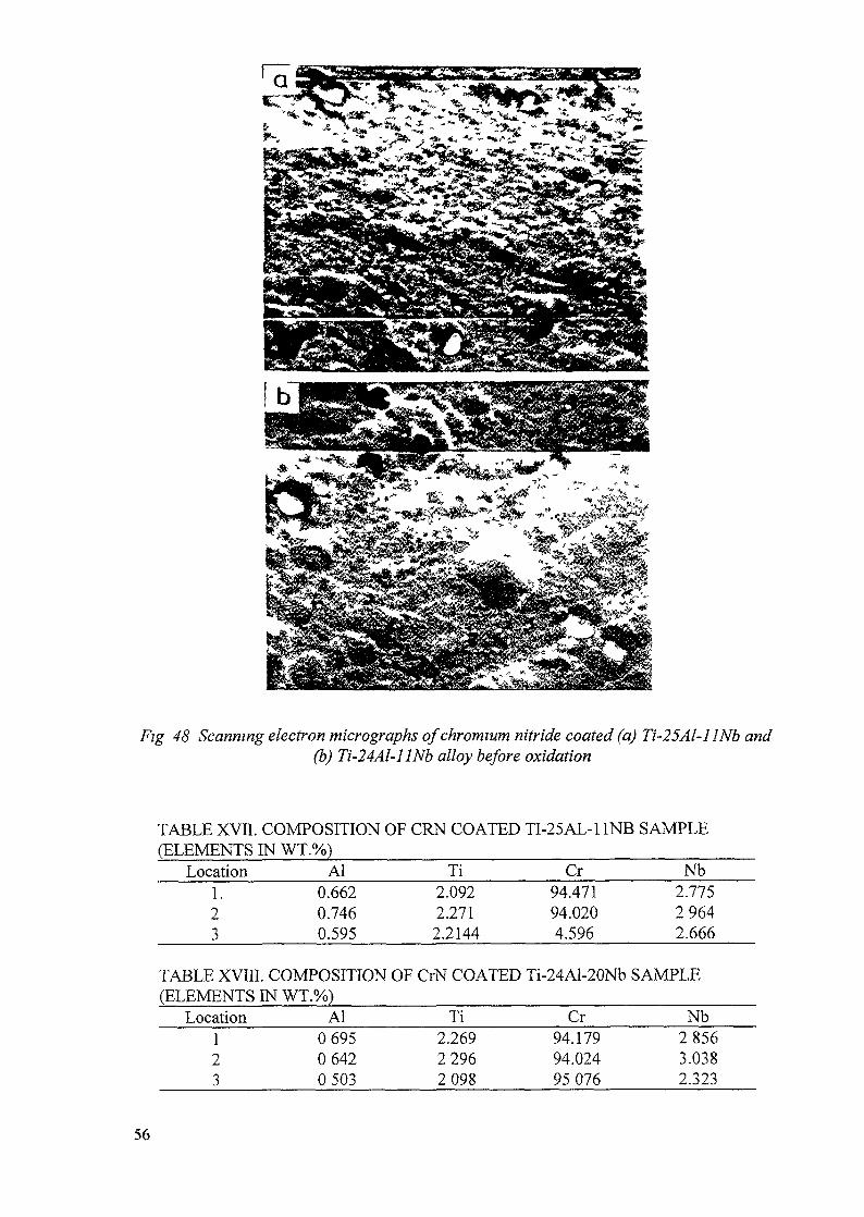
¥5 Scanning electron micrographs of chromium nitride coated (a) Ti-25Al-llNb and(b) Ti-24Al-llNb alloy before oxidation
TABLE XVII. COMPOSITION OF CRN COATED TI-25AL-11NB SAMPLE(ELEMENTS IN WT.%)
Location1.23
Al0.6620.7460.595
Ti2.0922.2712.2144
Cr94.47194.0204.596
Nb2.77529642.666
TABLE XVIII. COMPOSITION OF CrN COATED Ti-24Al-20Nb SAMPLE(ELEMENTS IN WT.%)
Location123
Al069506420503
Ti2.26922962098
Cr94.17994.02495076
Nb28563.0382.323
56

FIG. 49. SEM micrograph and X ray area scan maps ofN, Crfor the chromium nitridedTi-25Al-llNb alloy.
TABLE IXX. COMPOSITION OF PLASMA NITRIDED COATED T1-25A1-11Mb SAMPLE(ELEMENTS IN WT.%)_______________________________
Location Al Ti Nb1234
8.6314.8944.9024.988
52.31556.57556.06255.780
39.05438.53139.03639.23?
The compositional analysis by EDAX confirms that during plasma nitriding, TiN is themain coating. However, large amount of Al and Nb is also found in the coating.
57
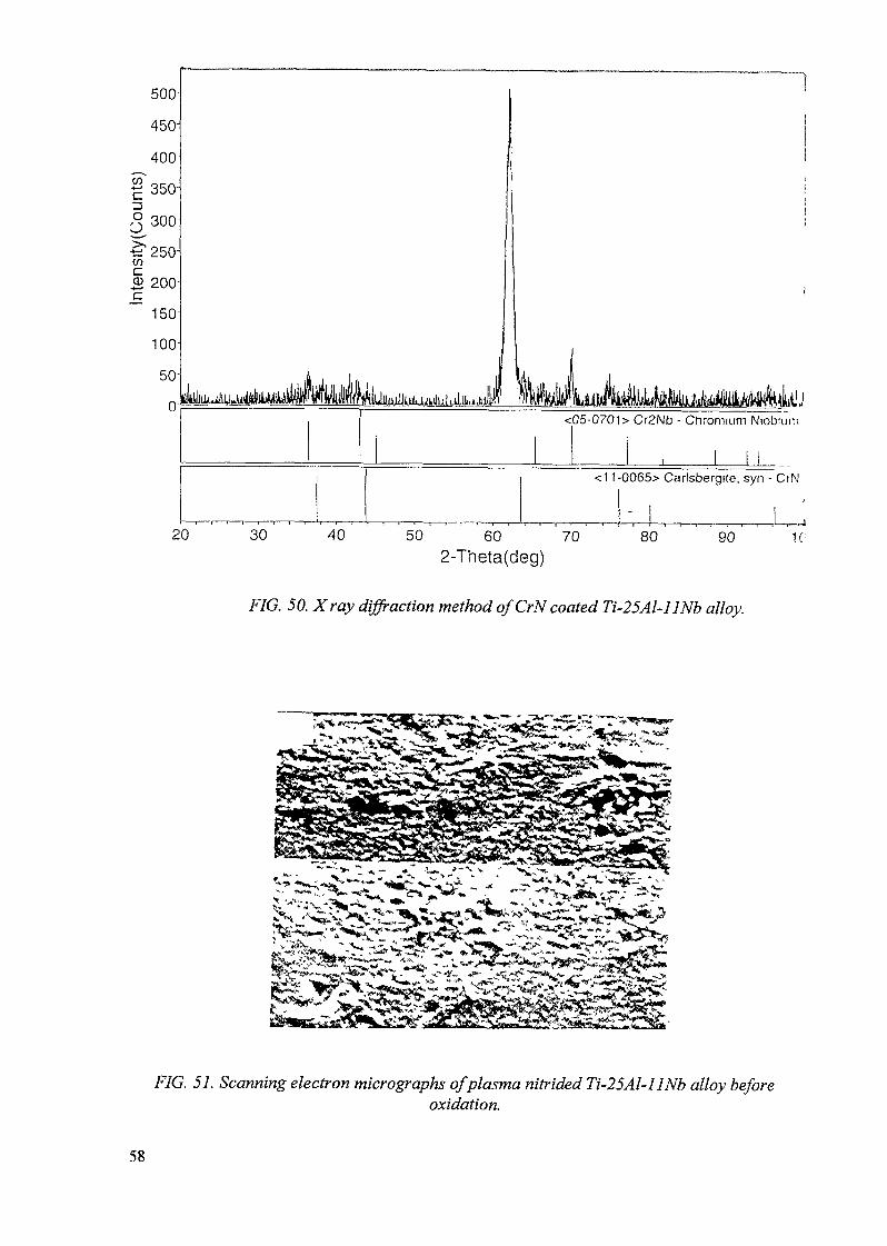
500-
450-
400
~ 3501
^ 300
IT250"1 200-
50-
0 m<05-0701> Cr2Nb - Chromium Niobium
<11-0065> Carlsbergite, syn - CfN
20 30 40 50 60 702-Theta(deg)
80 90 1C
FIG. 50. Xray diffraction method of CrN coated Ti-25Al-llNb alloy.
v--V--V-^-^.^* f -4 - v«:^T^V- ^ ,&j ^^^V4r. ~C^V*^Wb^* - - cT^? .*--4- ^^
t.
- ^ ^ . . *«- o - j
«s
F/G. 57. Scanning electron micrographs of plasma nitrided Ti-25Al-llNb alloy beforeoxidation.
58
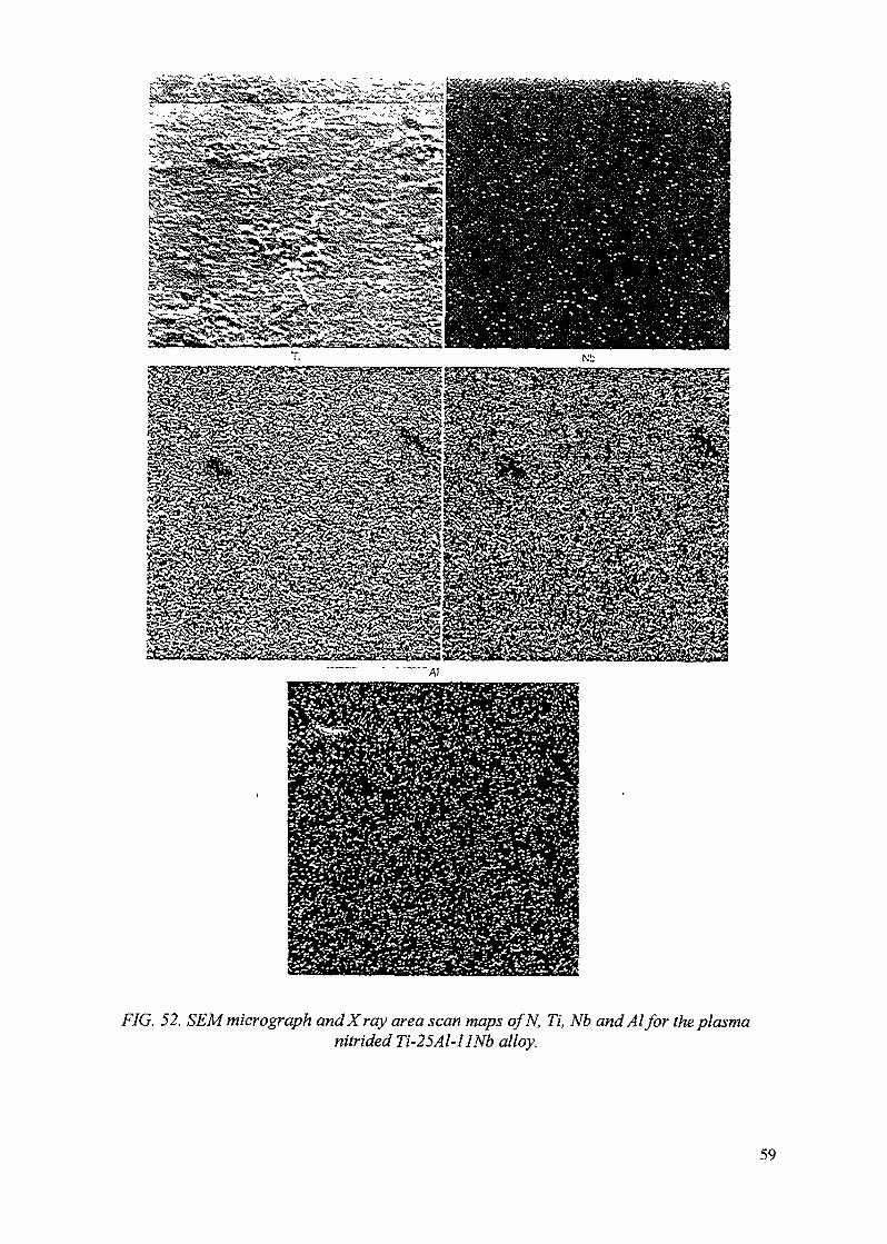
"*V&&\'K* -/*s*«» ^. '-^<--c^ - ;, *'&%'' ^^^t. , MrC'-v* ,ja».»-y-*x*M> ., . *. j y:<",.-^^_ -"^ «
F/G. 52. SEM micrograph and X ray area scan maps ofN, Ti, Nb and Al for the plasmanitrided Ti-25Al-llNb alloy.
59
250
<15-0598> AINb2 - Aluminum Niobium
<41-1352> TiNO 30 - Titanium Nitride
30 35 40 452-Theta(deg)
50 55 60
FIG. 53. Xray diffraction method of plasma nitrided Ti-25Al-llNb alloy.
4.16.7. Oxidation kinetics
Oxidation tests were carried out at 800°C in air for 100 hours. The weight changes vs.time plots for the oxidation of the base alloys Ti-25Al-llNb (Bl), Ti-24Al-20Nb (B2), andTi-22Al-20Nb (B3) are shown in Fig. 54. The oxidation kinetics appear to be parabolic innature. The parabolic rate constants for alloy Bl (Kp = 3.9xlO"3 mg^mV1) were found to besignificantly smaller compared to those of alloy B2 (Kp = 6.5xlO"3 mg^m^"1) and B3 (Kp =13xlO"3 mg2cmV).
The weight changes vs. time plots for the oxidation of CrN coated alloys Ti-25Al-l INb(CrNl), Ti-24Al-20Nb (CrN2), and Ti-22Al-20Nb (CrN3) at the same temperature in air aregiven in Fig. 55. The oxidation kinetics appears to be parabolic in nature. The parabolic rateconstants for alloy CrNl (Kp = 2.5xlO"3 mg2cni4h~1) were found to be smaller compared tothose of alloy CrN2 (Kp = 3.5X10"4 mg2cmV) and CrN3 (Kp = 5.15 (10" mgWrf J). Theoxidation kinetics for the CrN coated alloys follows a similar trend as for the base alloys,however, the overall weight gain is much lower for CrN coated alloys, indicating theimprovement in the oxidation resistance.
The weight changes vs. time plots for oxidation of plasma nitrided alloys Ti-25Al-l INb(PNl), Ti-24Al-20Nb (PN2), and Ti-22Al-20Nb (PN3) at 800°C in air are depicted in Fig. 56rThe oxidation kinetics appears to be parabolic in nature. The parabolic rate constant for alloyPNl (Kp = 1.6xlO~3 mg2cm4h~'1) were found to be smaller compared to those of alloy PN2(Kp = 2.6xlO~3 mg^mV1) and PN3 (Kp = 8.7xlO~3 mg2cmV'). The alloy PNl again shows
60
1.2 i
0.2--
20 40 60
Time (hrs)80 100 120
FIG. 54. Oxidation of base Ti$Al-Nb alloys at 800 °C in air.
0.18
20 40 60
Time (hrs)80 100 120
FIG. 55. Oxidation of Cr-Nitrided TisAl-Nb alloys at 800 °C in air.
61
20 40 60
Time (hrs)80 100 120
FIG. 56. Oxidation of plasma nitrided Ti^Al-Nb alloys at 800 °C in air.
20 40 60 80V
Time (hrs)100 120
FIG. 57. Oxidation ofAl/Ar ion beam mixed TisAl-Nb alloys at 800 °C in air.
62
the lowest oxidation rate among the three alloys. The overall weight gain is lower for plasmanitrided alloys than the base alloys, however, it is higher than the chromium nitrided coatedalloys. This shows that the nitrided coating using plasma technique improves the oxidationresistance of the base alloys but it is relatively less effective than the CrN coating made byplasma arc process.
Figure 57 shows the weight change vs. time plots for the oxidation of Al/Ar+ ion beammixed alloys Ti-25Alll-Nb (TO1), Ti-24AI-20Nb (ffi2), and Ti-22Al-20Nb (IBS). Theoxidation kinetics appears to be parabolic in nature. The parabolic rate constant for alloy IB 1(Kp = 3.3xlO~3 mg2cm4rfJ) was found to be smaller compared to those of alloy IB2 (Kp = 3.6xlO"3 mg2cm4h~1) and EB3 (Kp = 41xlO~3 mg2cmV1). The weight change follows a similartrend as in the case of the base alloy. The weight gains for the coated alloys are lower than thebase alloys, however, the improvement in oxidation resistance is lower than the plasmanitrided or CrN plasma arc process. In the case of Ti-22Al-20Nb (IBS) sample, higher weightgains are found. This might be due to some defects, which were found in the base alloy beforecoating.
It is of great interest to note that the chromium nitride coated samples were found tohave even better oxidation resistance than the plasma nitrided and Al/Ar+ ion beam mixedsamples. Thus it can be said that the chromium nitride coating can be highly beneficial forimproving the oxidation resistance of these alloys at high temperatures.
Scanning electron micrographs of the base alloy Ti-25Al-llNb, CrN coated alloy,plasma nitrided and ion beam mixed Al coated alloy specimens, after oxidation in air at 800°Cfor lOOh are depicted in Fig. 58. Local growth of oxide scale is evident in the case of the basealloy (Fig. 58a). Oxide scales formed on chromium nitrided and Al/Ar+ ion beam mixedspecimen was uniform and compact. Some pores in oxide scale were found in the case ofplasma nitrided Ti-25Al-l INb specimen (Fig. 58c).
Figure 59 shows the oxide morphologies of the base alloy Ti-24Al-20Nb, CrN coated,plasma nitrided and ion beam mixed Al coated specimens, after oxidation in air at 800°C for100 h Dense pillar-like grains of oxide can be seen on CrN sample (Fig. 59b). Oxide scale wasfound to be compact and uniform in the case of the base alloy, plasma nitrided and ion beammixed specimens. However, some pores in oxide scale were also found in the case of plasmanitrided specimen (Fig. 59c).
The scanning electron micrographs of base alloy Ti-22Al-20Nb, CrN coated, plasmanirtrided and ion beam mixed Al coated alloy specimens, after oxidation in air at 80 for 100 hare depicted in Fig. 60. Oxide scale characteristics were similar to that observed in the case ofTi-25Al-l INb alloys.
4.17. FORMATION OF WEAR-RESISTANT COMPOSITE SURFACE LAYERS
Layer composition: C-Me (Zr, Ti, Ta), C-N and B-N.
Substrates: AISI M2 high speed steel (0.86% C, 6.0% W, 5.0% Mo, 4.1% Cr, 1.9% V,0.5% Co, in wt.%); Al and Fe; carbon steel.
Ion beam technologies:
— Conventional ion implantation (CII).
63
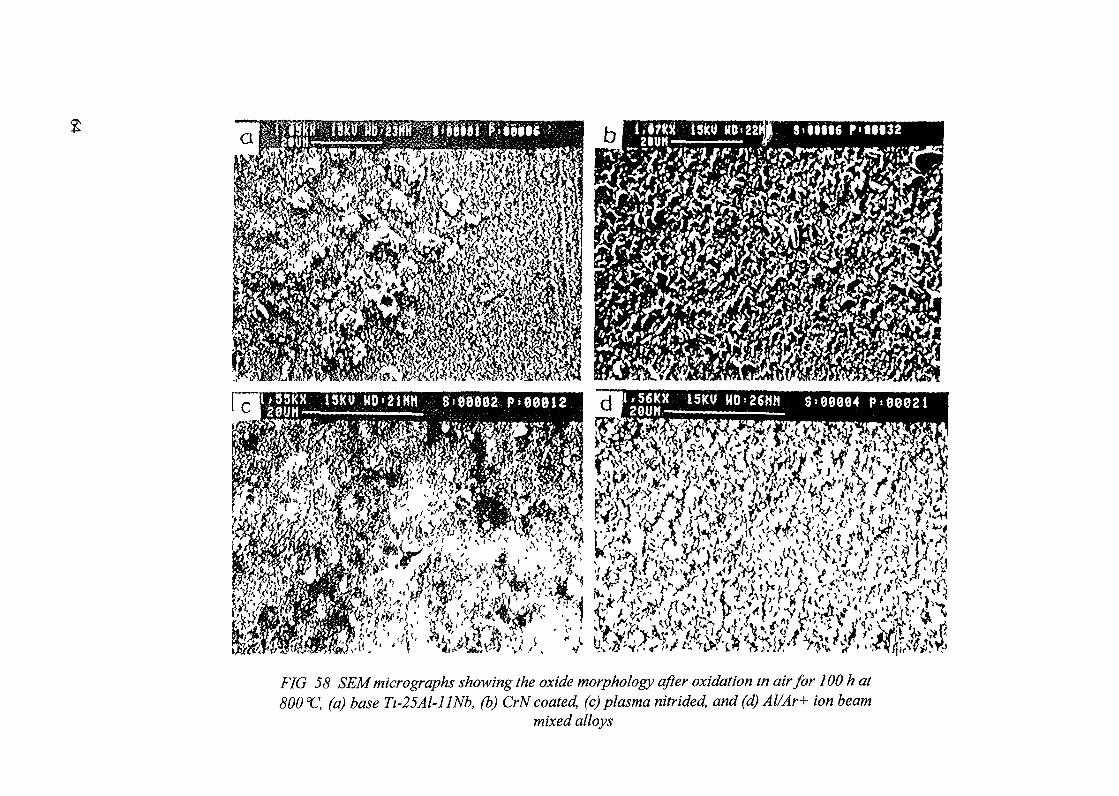
FIG 58 SEM micrographs showing the oxide morphology after oxidation in air for 100 hat800V, (a) base Ti-25Al-UNb, (b) CrN coated, (c) plasma nitrided, and (d) Al/Ar+ ion beam
mixed alloys
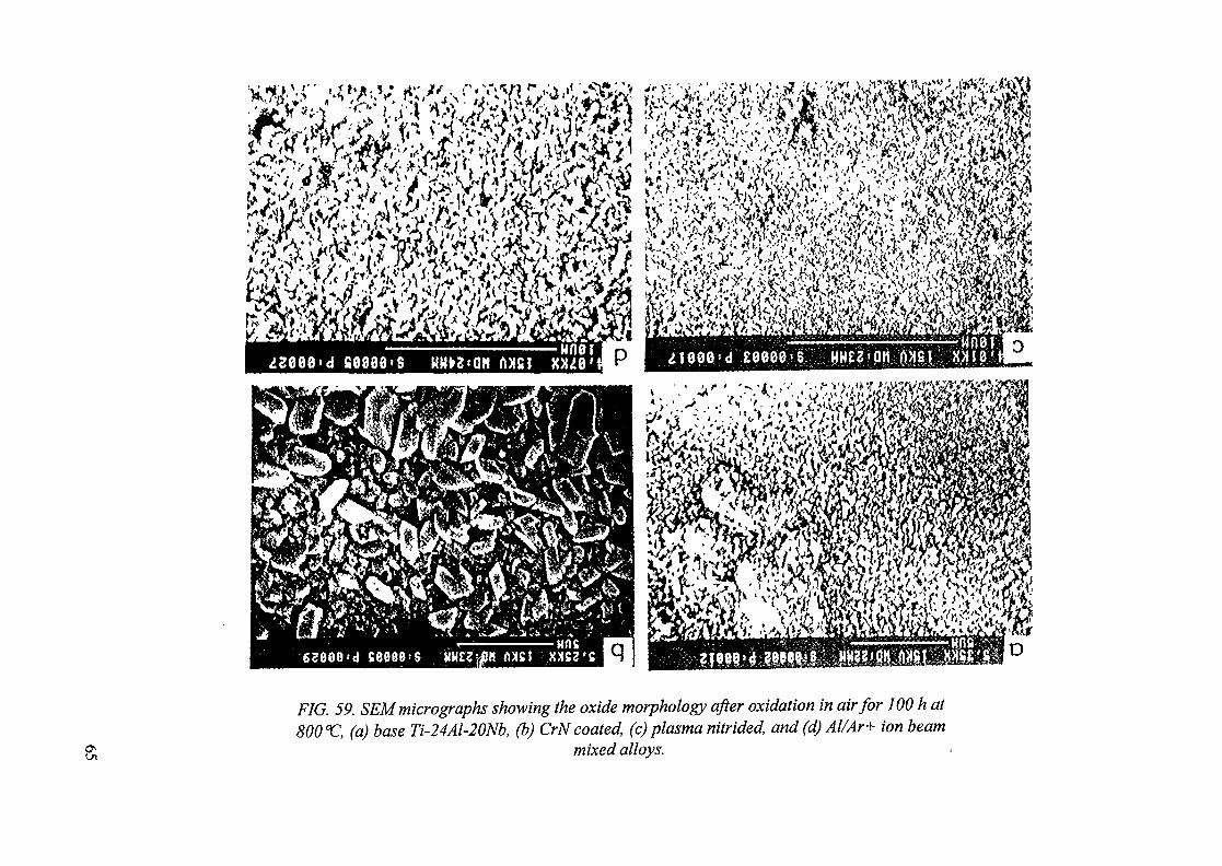
D
F/G. 5P. SEM micrographs showing the oxide morphology after oxidation in air for 100 hat800 T, ^ *«s« Ti-24Al-20Nb, (b) CrN coated, (c) plasma nitrided, and(d)Al/Ar+ ion beam
mixed alloys.
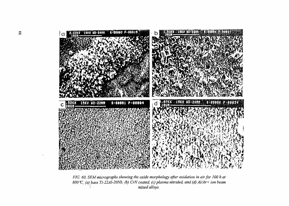
FIG. 60. SEM micrographs showing the oxide morphology after oxidation in air for 100 hat800V, (a) base Ti-22Al-20Nb, (b) CrN coated, (c) plasma nitrided, and (d) Al/Ar+ ion beam
i mixed alloys.

— Double ion implantation (DII) I high current ion implantation (HCII).— Coatings deposition by SVETLJACHOK source.
TREATMENT REGIMES
Method/Source
CIIHCII
MEVVASVETL.
Ion
B + NN + BC + Zr
C + Me (Zr,Ta, Ti)
Energy, keV
24,60 + 75,921+20
20 + 2520 + 25
Currentdensity,MA/cm2
1.5 + 1.53500 + 530
20 + 4011+6
Dose, ions/cm2 Temperature,°C
3-1017+3.6-1017
7-1019 + 2-1018
2-1017 + 2-1017
2-1017 + 2'1017
RT500350RT
Auger electron spectroscopy (AES); X ray diffraction (XRD); glancing X ray diffraction(GXRD); transmission electron microscopy (TEM); conversion electron Mossbauerspectroscopy (CEMS, scanning depth of O.l(um), conversion X ray Mossbauer spectroscopy(CXMS, scanning depth of 10(jJ.m); X ray photoelectron spectroscopy (XPS); microhardnessand nanohardness, friction (pin-on-plane and pin-on-disk), and wear measurements were used.
4.17.1. Element composition
— Dn and coating deposition by SVETLJACHOK source allow to form compositeuniform and layer surface structure with elements concentration strongly depending onirradiation energy, current density, dose and sequence of implantation;
— HCII of nitrogen and boron leads to deep (up to 20(0.m) penetration of nitrogen into AISIM2 steel and forms surface boron layer with thickness of about 0.3u,m on top ofnitrogen containing layer;
— The forming profiles of nitrogen and boron strongly depend on sequence ofimplantations by HCII methods. This is due to strong sputtering during N implantationand boron surface accumulation during B implantation;
— Carbon coating with thickness of up to 0.25 (im containing up to 20 at.% of metal (Zr,Ta, Ti) by SVETLJACHOK source.
4.17.2. Phase composition and microstructure
(1) Phase composition of near-surface (0.1|im, GXRD, CEMS) and deep (~10|im, CXMS)layers (Table XX) formed by HCJI is superposition of £-Fe3N, a"-Fei6N2, a-Fe (C, N)and FeB phases.
(2) Irradiation using SVETLJACHOK source leads to formation of amorphous carboncoating with ZrC carbide precipitates in it and %-Fe2C carbide in interface of coating andsubstrate.
(3) AES and XPS spectra of iron after DU of boron and nitrogen are indicative of possibleboron nitrides formation in the concentration region of 10-18 at.% after successiveboron and nitrogen CII.
67

TABLE XX. PHASE COMPOSITION OF AISI M2 STEEL AFTER HCII OF NITROGENAND BORON IONS
SampleN
N + B
depth ^m0.10.1100.110
share in spectrum, %cc-Fe(C)95, y-Fe(C) 5
cc-Fe(C,N) 76, y-Fe(QN) 3, e-Fe3N 21a-Fe(C,N) 66, y-Fe(C,N) 4, e-Fe3N 20, a"-Fei6N2 10
a-Fe(C,N) 55, y-Fe(C,N) 4, e-Fe3N 29, a"-Fei6N2 6, FeB 7a-Fe(C,N) 49, y-Fe(C,N) 6, e-Fe3N 36, a"-Fe]6N2 10
4.17.3. Mechanical properties
(1) Double HCII of nitrogen and boron increases hardness and decreases friction coefficientby a factor of 2. The enhanced hardness is observed up to a depth of 20 (im.
(2) HCII of nitrogen greatly changes roughness of steel from 0.01 \im to 0.6 fim due tostrong sputtering by nitrogen ions. Additional boron implantation decreases roughnessdown to 0.25|0,m due to deposition of boron film.
(3) Decrease of friction coefficient of AISI M2 steel by a factor of 6 down to 0.1 andincrease of wear-resistance by a factor of 4 after irradiation using SVETLJACHOKsource.
(4) High hardness of C-Zr composite layers formed by SVETLJACHOK source.
(5) Increase of aluminium lifetime by a factor of 100 after deposition of carbon coating innitrogen atmosphere due to possible formation of C-N bonds.
From the above it may be concluded that:
— Composite surface layers formed by double HCII and by SVETLJACHOK sourcepossess beneficial mechanical properties (high hardness and wear-resistance, lowfriction coefficient).
— Double ion implantation of boron and nitrogen into iron is possible method of BNnitride formation.
— Comparison analysis of high speed steel modified by various methods (MEVVA, HCn,SVETLJACHOK) has shown that the composite carbon 20Zr80C layers formed bySVETLJACHOK source are the most wear-resistant.
4.18. DETERMINATION OF THE H CONTENT IN DIAMOND FILMS GROWN BYCVD AND ITS INFLUENCE ON THE COEFFICIENT OF THERMALCONDUCTIVITY (K) OF THE FILMS
The thin films of diamond are grown using chemical vapour deposition techniques. Thehot filament chemical vapour deposition (HFCVD) technique is used to grow the films of thethickens ranging from 3-40 micron. The detailed diagram of the deposition apparatus isshown in Fig. 61. A detailed structural, electrical and mechanical characterization of the filmshave been carried out. Various deposition parameters are optimized so as to^grow the state-of-the-art films. We observe that the deposition pressure is a very important parametercontrolling the non-diamond impurities in the films. The films grown at low depositionpressure (20-40 torr) show white translucent colour with almost zero non diamond carbonimpurities as observed by Raman spectroscopy. The X ray diffraction (XRD) is employed to
68
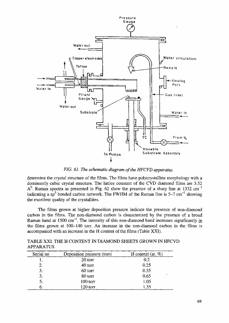
PressureGauge
Water out
Water circulationCopper electrodes
T Y^ Teflon
Water in
To PumpsMovableSubstrate Assembly
FIG. 61. The schematic diagram of the HFCVD apparatus.
determine the crystal structure of the films. The films have polycrystalline morphology with adominantly cubic crystal structure. The lattice constant of the CVD diamond films are 3.52A°. Raman spectra as presented in Fig. 62 show the presence of a sharp line at 1332 cm"1
indicating a sp3 bonded carbon network. The FWHM of the Raman line is 5-7 cm"1 showingthe excellent quality of the crystallites.
The films grown at higher deposition pressure indicate the presence of non-diamondcarbon in the films. The non-diamond carbon is characterized by the presence of a broadRaman band at 1500 cm"1. The intensity of this non-diamond band increases significantly inthe films grown at 100-140 torr. An increase in the non-diamond carbon in the films isaccompanied with an increase in the H content of the films (Table XXI).
TABLE XXI. THE H CONTENT IN DIAMOND SHEETS GROWN IN HFCVDAPPARATUS
Serial no1.2.3.3.5.6.
Deposition pressure (torr)20 torr40 torr60 torr80 torr100 torr120 torr
H content (at. %)0.20.250.350.651.051.35
69
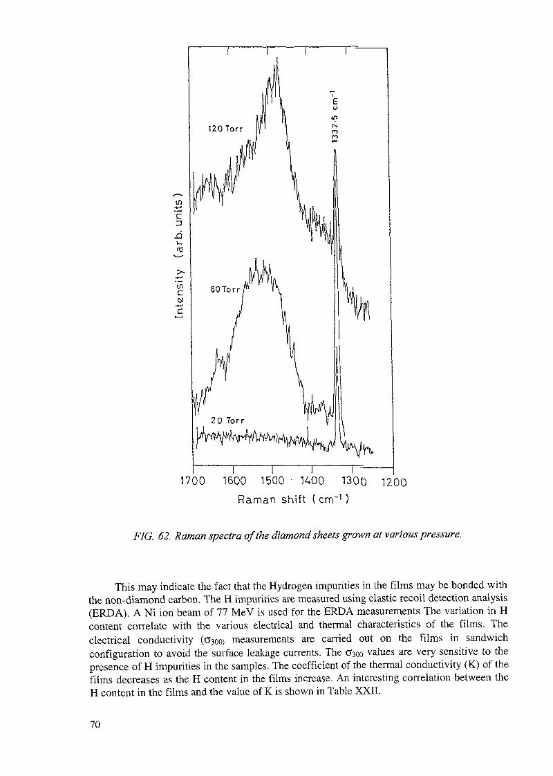
1700 1600 1500 • 1400 1300 1200Raman shift ( cm"1)
FIG. 62. Raman spectra of 'the diamond sheets grown at various pressure.
This may indicate the fact that the Hydrogen impurities in the films may be bonded withthe non-diamond carbon. The H impurities are measured using elastic recoil detection analysis(ERDA). A Ni ion beam of 77 MeV is used for the ERDA measurements The variation in Hcontent correlate with the various electrical and thermal characteristics of the films. Theelectrical conductivity (a30o) measurements are carried out on the films in sandwichconfiguration to avoid the surface leakage currents. The G3oo values are very sensitive to thepresence of H impurities in the samples. The coefficient of the thermal conductivity (K) of thefilms decreases as the H content in the films increase. An interesting correlation between theH content in the films and the value of K is shown in Table XXII.
70
TABLE XXII. THE THERMAL CONDUCTIVITY VALUES AND ATOMIC % OF H INTHE SHEETS
serial no123456
deposition pressure20 torr30 torr40 torr60 torr80 torr100 torr
atomic % of H0.2
0.250.350.65
1
K ( watt/cm °K )15
121085
In addition to the above, serious attempts have also been made to enhance the adhesionof the diamond films with the stainless steel substrates for the diamond tool applications. Wefind that a buffer layer of a mixture of NiCr prove to be very effective in enhancing theadhesion of the films. In the co-ordination program the Raman spectra and ERDA analysis arecarried out on the CrN films supplied by the agency. The CrN coated substrates have beencoated with the CVD diamond films. The characteristics of the diamond coated on CrNdeposited SS substrates are compared with the films deposited on bare SS.
5. ROUND ROBIN TEST ON EVALUATION AND PERFORMANCE OF ION BEAMASSISTED CHROMIUM NITRIDE COATING ON STAINLESS STEEL
SUBSTRATE
Stainless steel coupons of 20 mm diameter and 2 mm thickness were cut from acontrolled lot of an AISI type 304 stainless steel bar. These samples were then polished to amirror finish using a series of standard metallurgical polishing steps. 300 polished sampleswere then loaded into a planetary system for rotation and translation to receive a uniformchromium nitride coating.
IBAD system of SPIRE Corporation, USA, was used for this purpose, which is shownschematically in Fig. 63. The system consists of a chamber with two independent systems, onefor deposition of Cr by electron beam evaporation and, from the other, an intense beam oTN ions is bombarded at an operating voltage of 1000 eV. Vacuum level of the chamber wasmaintained at 5 x 10~7 torr. Extensive experience at SPIRE Corporation has shown that achromium rich chromium nitride coating is better than stoichiometric CrN for tribologicalapplications. Also, temperature of the substrate has been controlled to obtain the best coatingperformance.
Chromium nitride was chosen as the coating of choice for several reasons: a) it is a fullydeveloped and optimized coating offered by SPIRE Corporation with extensive laboratorytesting behind it, b) it is a hard, wear-resistant coating for challenging industrial applicationsand, c) it is chemically inert and is ideal coating for corrosion testing.
The samples are characterized by RBS, AES, AFM, XPS, XRD and Glancing XRDmethods and evaluated by tribological, microhardness, dynamic micro-indentation, impact,scratch, dry sliding, friction wear and corrosion tests.
71
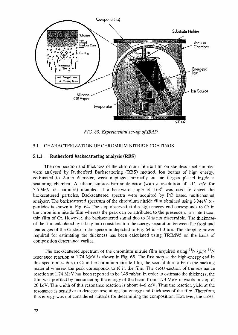
Component (s
Substrate Holder
VacuumChamber
EnergeticIons
Ion Source
921617
FIG. 63. Experimental set-up oflBAD.
5.1. CHARACTERIZATION OF CHROMIUM NITRIDE COATINGS
5.1.1. Rutherford backscattering analysis (RBS)
The composition and thickness of the chromium nitride film on stainless • steel sampleswere analysed by Rutherford Backscattering (RBS) method. Ion beams of high energy,collimated to 2-mm diameter, were impinged normally on the targets placed inside ascattering chamber. A silicon surface barrier detector (with a resolution of -11 keV for5.5 MeV a -particles) mounted at a backward angle of 168° was used to detect thebackscattered particles. Backscattered spectra were acquired by PC based multichannelanalyser. The backscattered spectrum of the chromium nitride film obtained using 3 MeV a -particles is shown in Fig. 64. The step observed at the high energy end corresponds to Cr inthe chromium nitride film whereas the peak can be attributed to the presence of an interfacialthin film of Cr. However, the backscattered signal due to N is not discernible. The thickness-of the film calculated by taking into consideration the energy separation between the front andrear edges of the Cr step in the spectrum depicted in Fig. 64 is -1.3 |im. The stopping powerrequired for estimating the thickness has been calculated using TRIM'95 on the basis ofcomposition determined earlier.
The backscattered spectrum of the chromium nitride film acquired using 14N (p,p) 14Nresonance reaction at 1.74 MeV is shown in Fig. 65. The first step at the high-energy end inthis spectrum is due to Cr in the chromium nitride film, the second due to Fe in the backingmaterial whereas the peak corresponds to N in the film. The cross-section of the resonancereaction at 1.74 MeV has been reported to be 145 mb/sr. In order to estimate the thickness, thefilm was profiled by incrementing the energy of the beam from 1.74 MeV onwards in step of20 keV. The width of this resonance reaction is about 4-6 keV. Thus the reaction yield at theresonance is sensitive to detector resolution, ion energy and thickness of the film. Therefore,this energy was not considered suitable for determining the composition. However, the cross-
72
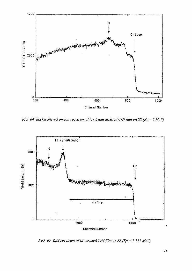
4UOU
3
.2
2000 .
2DO 400 600
Channel Number
800 1000
FIG 64 Backscattered proton spectrum of ion beam assisted CrNfllm on SS (Ea = 3 MeV)
1000 150Q
Channel Number
FIG 65 RBS spectrum of IB assisted CrNfllm on SS (Ep = 1 711 MeV)
73
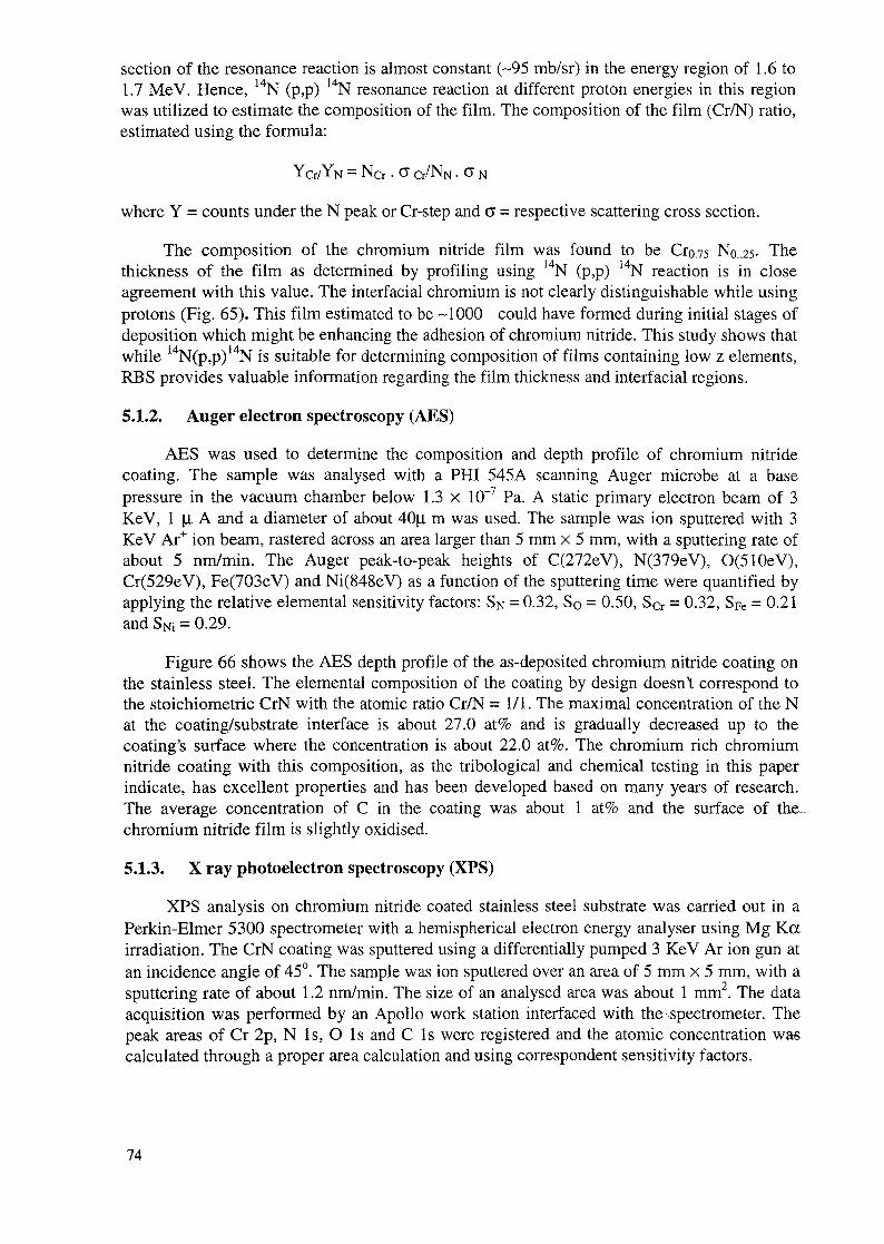
section of the resonance reaction is almost constant (-95 mb/sr) in the energy region of 1.6 to1.7 MeV. Hence, 14N (p,p) I4N resonance reaction at different proton energies in this regionwas utilized to estimate the composition of the film. The composition of the film (Cr/N) ratio,estimated using the formula:
YCr/YN = NCr. a Cr/NN. a N
where Y = counts under the N peak or Cr-step and o = respective scattering cross section.
The composition of the chromium nitride film was found to be Cro.?5 No..25- Thethickness of the film as determined by profiling using 14N (p,p) 14N reaction is in closeagreement with this value. The interfacial chromium is not clearly distinguishable while usingprotons (Fig. 65). This film estimated to be -1000 could have formed during initial stages ofdeposition which might be enhancing the adhesion of chromium nitride. This study shows thatwhile 14N(p,p)14N is suitable for determining composition of films containing low z elements,RBS provides valuable information regarding the film thickness and interfacial regions.
5.1.2. Auger electron spectroscopy (AES)
AES was used to determine the composition and depth profile of chromium nitridecoating. The sample was analysed with a PHI 545A scanning Auger microbe at a basepressure in the vacuum chamber below 1.3 x 10~7 Pa. A static primary electron beam of 3KeV, 1 (0, A and a diameter of about 40|i m was used. The sample was ion sputtered with 3KeV Ar+ ion beam, rastered across an area larger than 5 mm x 5 mm, with a sputtering rate ofabout 5 nm/min. The Auger peak-to-peak heights of C(272eV), N(379eV), O(510eV),Cr(529eV), Fe(703eV) and Ni(848eV) as a function of the sputtering time were quantified byapplying the relative elemental sensitivity factors: SN = 0.32, So = 0.50, Scr = 0.32, Spe = 0.21and SNi = 0.29.
Figure 66 shows the AES depth profile of the as-deposited chromium nitride coating onthe stainless steel. The elemental composition of the coating by design doesn't correspond tothe stoichiometric CrN with the atomic ratio Cr/N = 1/1. The maximal concentration of the Nat the coating/substrate interface is about 27.0 at% and is gradually decreased up to thecoating's surface where the concentration is about 22.0 at%. The chromium rich chromiumnitride coating with this composition, as the tribological and chemical testing in this paperindicate, has excellent properties and has been developed based on many years of research.The average concentration of C in the coating was about 1 at% and the surface of the_chromium nitride film is slightly oxidised.
5.1.3. X ray photoelectron spectroscopy (XPS)
XPS analysis on chromium nitride coated stainless steel substrate was carried out in aPerkin-Elmer 5300 spectrometer with a hemispherical electron energy analyser using Mg Kairradiation. The CrN coating was sputtered using a differentially pumped 3 KeV Ar ion gun atan incidence angle of 45°. The sample was ion sputtered over an area of 5 mm x 5 mm, with asputtering rate of about 1.2 nm/min. The size of an analysed area was about 1 mm2. The dataacquisition was performed by an Apollo work station interfaced with the spectrometer. Thepeak areas of Cr 2p, N Is, O Is and C Is were registered and the atomic concentration wascalculated through a proper area calculation and using correspondent sensitivity factors.
74

0)£oO
100 -
80 -
60 -
40 -
20 -
0
N
O
0 20 40 60 .80 100 120 140 160 180 200 220
Sputter Time (min)
FIG. 66. AES sputter depth profile of the CrN coated SS.
Contrary to the AES results, the XPS analysis showed in the CrN coating besides thecarbon the presence of oxygen was also noticed (Fig. 67). In the XPS spectra, thecorresponding peaks of N Is at 396.6 V (Fig. 67b) O Is at 529.5 eV (Fig. 67c) and C Is at281.9 eV (Fig. 67d) are characteristic for Cr nitride, oxide and carbide, respectively. XPSsputter depth profiling revealed inside of the CrN coating the following composition: 75 at%Cr, 16.0 at% N, 5 at% O and 4 at% C.
5.1.4. X ray diffraction analysis (XRD)
The X ray diffraction of chromium nitride coated SS 304 showed that the structure ofchromium nitride coating is amorphous, not crystalline. The amorphous pattern can Be"observed very clearly from the XRD spectrum, as shown in Fig. 68. X ray diffraction of AISI304 SS is also shown in Fig. 69, which reveals that chromium nitride coating consists mainlyof Cr2N phase (28 at. % Of N) and some quantity of pure Cr is also present in coating. Thepresence of CrN phase can not be determined unambiguously because CrN diffraction linesoverlap that of CraN and substrate y — (Fe, Cr, Ni).
5.1.5. Glancing angle X ray diffraction
The results of Glancing X ray analysis of chromium nitride coated stainless steelsamples are given in Fig. 70. These results confirm the coating as Cr2N with grain size of 5 ±2 nm. It also confirms that the thickness of coating is equal to around 1.2 |im, which is alsoconfirmed by RBS method.
75
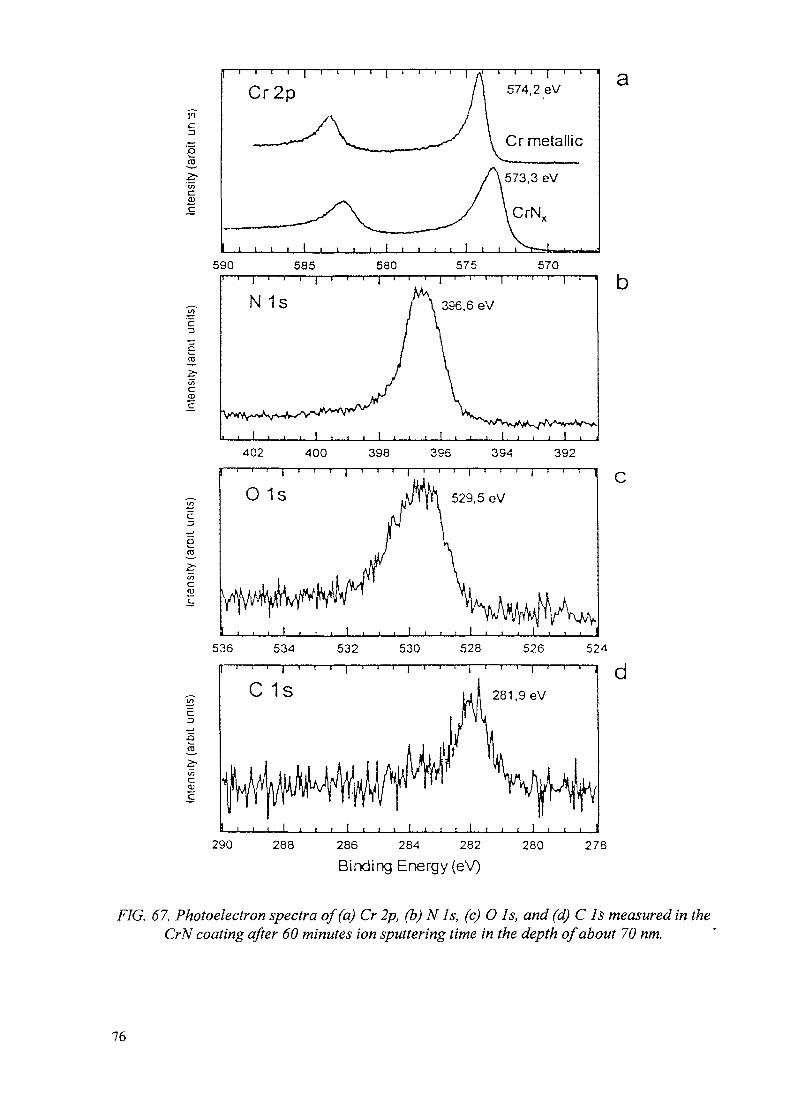
Itc
-QCD
590 585 580 575 570
C13
CS'c
N 1s 396,6 eV
402 400 398 396 394 392
VJc
o03
c<u
536 534 532 530 528 526 524
ro2?V)c
c
C 1s
290 288 286 284 282Binding Energy (eV)
280 278
FIG. 67. Photoelectron spectra of (a) Cr 2p, (b) N Is, (c) O Is, and (d) C Is measured in theCrN coating after 60 minutes ion sputtering time in the depth of about 70 nm.
76
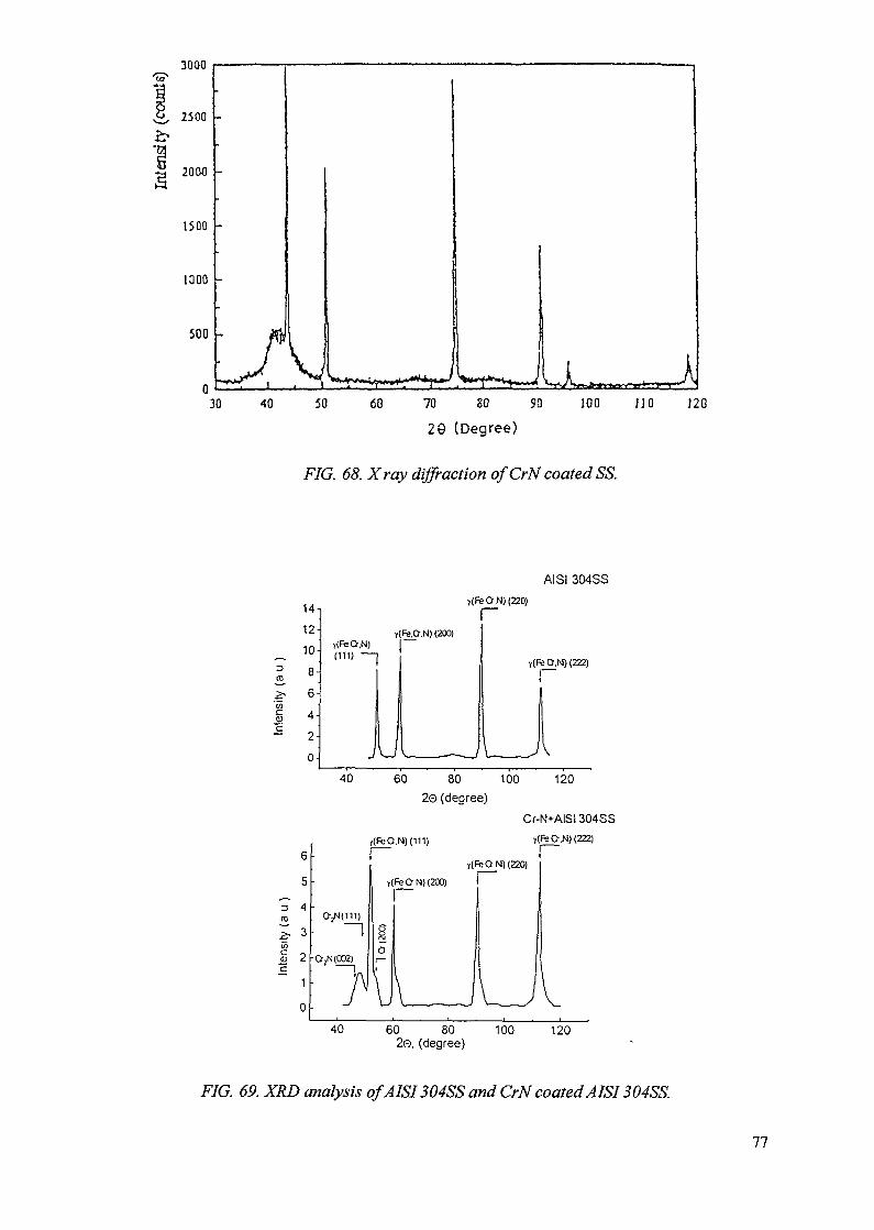
3000
2500 -
2000
1500
1000
500
30 40 50 <30 70 80 90
29 (Degree)
FIG. 68. Xray diffraction of CrN coated SS.
AISI 304SS
14
12-
10-
8-
6-
4-
20-
r(feON)(220)r~y(FeQ,M)(111) —
r(Fe.G.N) (200)
v(FeO,N)(222)
tfl
I_c
40 60 80 100 1202© (degree)
Cr-N+AISI 304SSv(FeO,N)(222)
O2N(C02)
40 60 80 100 12020, (degree)
FIG. 69. XRD analysis ofAISI 304SS and CrN coated AISI 304SS.
77
CrN (111) CrN (200)
Cr,N(110) Cr,N(002)
t; -I-t
Cr (200)
I
Cr2N (hep)
+ CCr / CN = 67 / 33 at.% [ASTM]* CCr / CN = 72 / 28 at.% (AES)
4> = 10
= 3° ~ 0.9
40 45 50 55 60 65
>, degree
F/G. 70. Glancing X ray analysis of CrN coated SS.
5.1.6. SEM/EDAX/AFM
Surface of chromium nitride coated SS 304 was analysed by scanning electronmicroscopy. The coating was found uniform and dense (Fig. 71). The composition of thechromium nitride layer as measured by ED AX is given in Table XXIII.
TABLE XXIII. CHEMICAL COMPOSITION OF VARIOUS ELEMENTS PRESENT INCOATING
Element
Fe
Corrosion
W.T.%
5.47
94.53
A.T.%
5.11
94.89
% S. E.
2.1
0.32
The atomic force microscopy (AFM) measurements were performed on a Topo-MetricsTMX 2000 Explorer in ambient conditions. In this equipment the cantilever with the tip scansover the fixed sample by means of piezoelectric drives. AFM provides a topography imageand quantitative topography information (Fig. 72). The most frequently used roughnessparameter is Ra, which is the arithmetic mean of the deviations in height from the profilemean value. The root mean square (RMS) roughness values based on the power spectraldensity, which is defined as the square magnitude of the Fourier Transform of the surfaceprofile.
78

FIG. 7}. Scanning Electron Micrographs ofCrN coated SS 304.
5.2. PERFORMANCE EVALUATION OF CHROMIUM NITRIDE COATING
5.2.1. Tribological and dynamic micro-indentation test
Tribological and micro-indentation tests were performed on chromium nitride coated SSsubstrate. The ball-on-disk friction and wear tests were performed i n ' a TRJBOMETERFALEX ISC 320. The general conditions of the test for ali the samples were the following:
— Ball material: AISI 52100 steel.— Ball diameter: 10.0 mm.
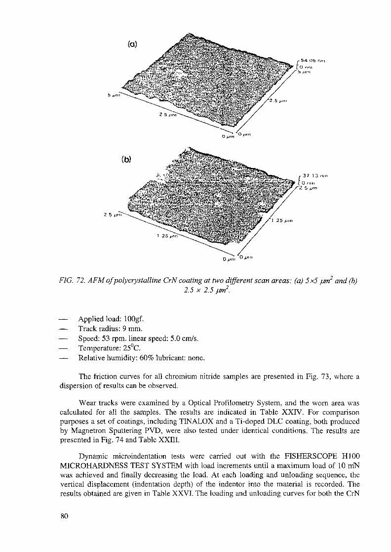
(a)54. O5 nm
3 7 1 3 .1.11
FIG. 72. AFM of polycrystalline CrN coating at two different scan areas: (a) 5x5 jum2 and (b)2.5 x 2.5
— Applied load: lOOgf.— Track radius: 9 mm.— Speed: 53 rpm. linear speed: 5.0 cm/s.— Temperature: 25°C.— Relative humidity: 60% lubricant: none.
The friction curves for all chromium nitride samples are presented in Fig. 73, where adispersion of results can be observed.
Wear tracks were examined by a Optical Profilometry System, and the worn area wascalculated for all the samples. The results are indicated in Table XXIV. For comparisonpurposes a set of coatings, including TINALOX and a Ti-doped DLC coating, both producedby Magnetron Sputtering PVD, were also tested under identical conditions. The results arepresented in Fig. 74 and Table XXIII.
Dynamic microindentation tests were carried out with the FISHERSCOPE HI00MICROHARDNESS TEST SYSTEM with load increments until a maximum load of 10 niNwas achieved and finally decreasing the load. At each loading and unloading sequence, thevertical displacement (indentation depth) of the indentor into the material is recorded. Theresults obtained are given in Table XXVI. The loading and unloading curves for both the CrN
80

1.88
8.08 —
e.&H -
0.40
8.28 -
ELHPSED T I M E ( m i n u t e s )
1.88
8.88 -
68.
FIG. 73. Friction curves obtained from CrN coated samples.
i r~i—i—|—i—r~i ' i—| i i i i—r—i—i—i—i—| i i i i ] i i i i i i i i i i i i i i j i
iKLfU'SED TIHF. ( m i n u t e s ) !
FIG. 74. Friction curves obtained fromAISI 52100 steel, CrN (sample 1), TINALOXandTi-DLC coated samples.
81

TABLE XXIV. WEAR AREAS OBTAINED BY OPTICAL LASER PROFILOMETRYFROM WORN CrN COATINGS
CrN coatings
Sample 1
Sample 2
Sample 3Sample 4Sample 5Sample 6
Wear tracks area
0.0000225
0.0000225
0.0000500
0.0000500
0.0000525
0.0000525
(mm2)
TABLE XXV. WORN AREAS MEASURED BY OPTICAL PROFILOMETRY
Materials/Coatings Wear track areas (mm )
AISI 52100 steel
CrN(samplel)
TINALOX
TI-DLC
0.0001025
0.0000225
0.0000475
0.0000275
coating (lower curves) and the corresponding substrate material (upper curves) are presentedin Fig. 75. In this figure it is clearly seen that the elastic recovery and hardness values for thecoating are significantly higher than the base material.
TABLE XXVI. DYNAMIC MICRO-INDENTATION RESULTS FOR CrN AND ITSSUBSTRATE MATERIAL
Vickers hardness at 10 mN
Relative elastic recovery
Total work (nj)
Elastic work (%)
Plastic work (%)
Young modulus (GPa)Plastic hardness (N/mm2)
CrN coating
16749 N/mm2
35.96 %
0.75
46.59
53.41
201
14373 N/mm2
Steel substrate
3728 N/mm2
8.48%
1.51
10.35
89.65
165
2549 N/mm2
82
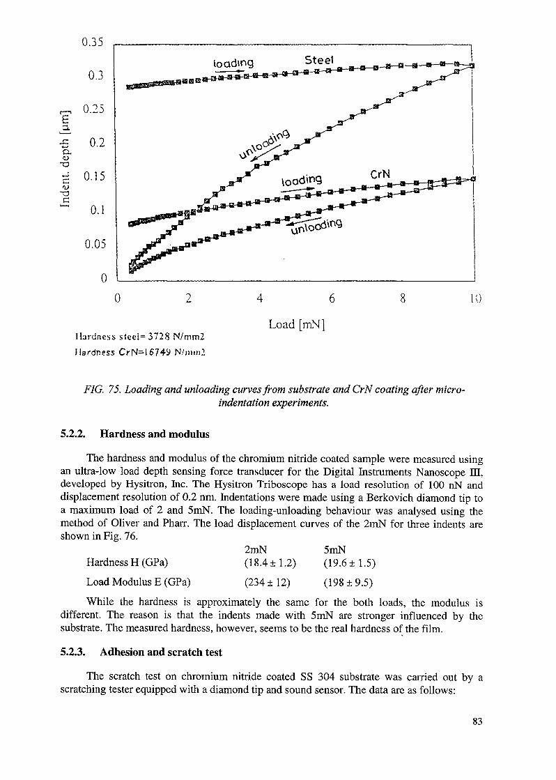
0.<u"O
X)c
0 2
Hardness stcel=3728 N/rnm2Hardness ON=16749 N/mm2
4 6
Load [mN]
75. Loading and unloading curves from substrate and CrN coating after micro-indentation experiments.
5.2.2. Hardness and modulus
The hardness and modulus of the chromium nitride coated sample were measured usingan ultra-low load depth sensing force transducer for the Digital Instruments Nanoscope IE,developed by Hysitron, Inc. The Hysitron Triboscope has a load resolution of 100 nN anddisplacement resolution of 0.2 nm. Indentations were made using a Berkovich diamond tip toa maximum load of 2 and 5mN. The loading-unloading behaviour was analysed using themethod of Oliver and Pharr. The load displacement curves of the 2mN for three indents areshown in Fig. 76.
2mN 5mNHardness H (GPa) (18.4 ± 1.2) (19.6 ± 1.5)
Load Modulus E (GPa) (234+12) (198 ±9.5)
While the hardness is approximately the same for the both loads, the modulus isdifferent. The reason is that the indents made with 5mN are stronger influenced by thesubstrate. The measured hardness, however, seems to be the real hardness of the film.
5.2.3. Adhesion and scratch test
The scratch test on chromium nitride coated SS 304 substrate was carried out by ascratching tester equipped with a diamond tip and sound sensor. The data are as follows:
83
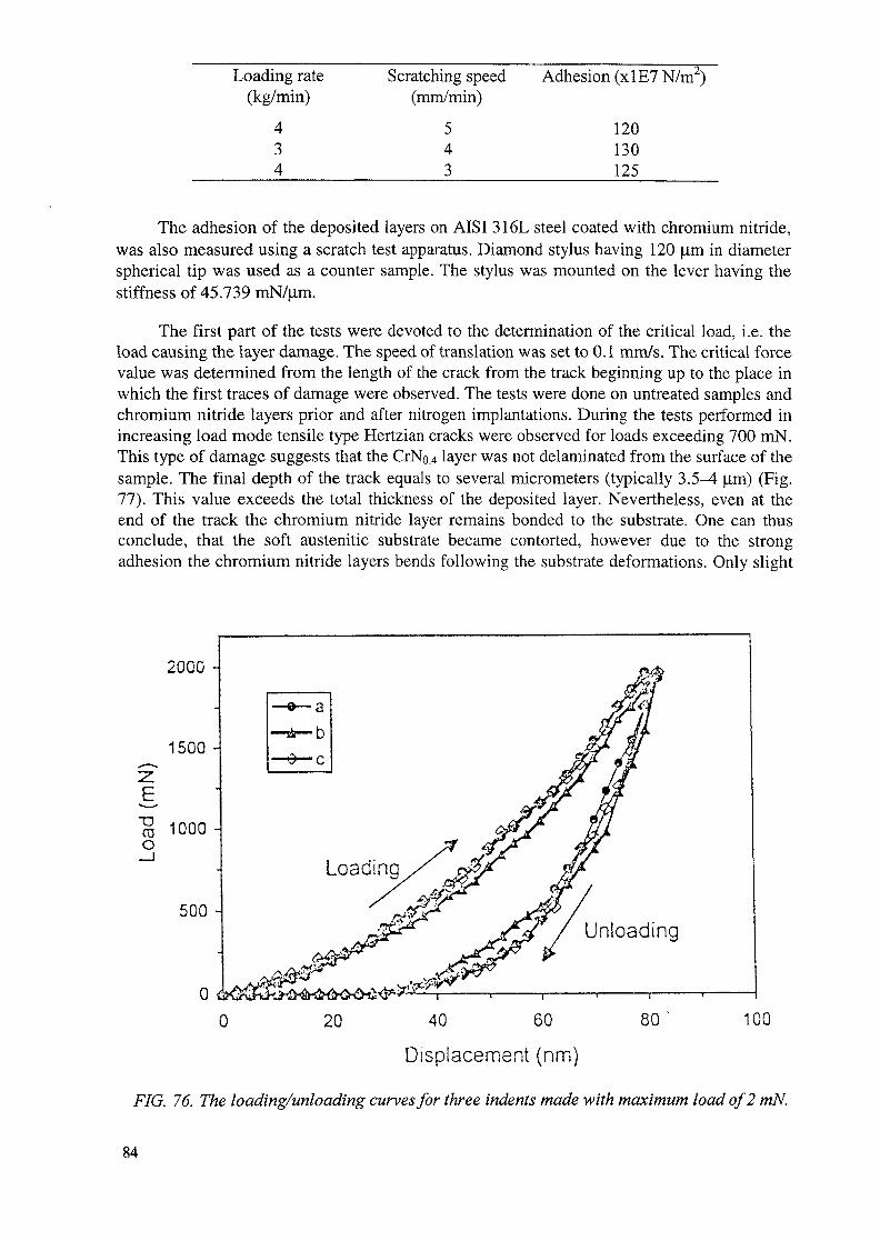
Loading rate(kg/min)
434
Scratching speed(mm/min)
543
Adhesion (xlE7N/m2)
120130125
The adhesion of the deposited layers on AISI 316L steel coated with chromium nitride,was also measured using a scratch test apparatus. Diamond stylus having 120 |im in diameterspherical tip was used as a counter sample. The stylus was mounted on the lever having thestiffness of 45.739 mN/|im.
The first part of the tests were devoted to the determination of the critical load, i.e. theload causing the layer damage. The speed of translation was set to 0.1 mm/s. The critical forcevalue was determined from the length of the crack from the track beginning up to the place inwhich the first traces of damage were observed. The tests were done on untreated samples andchromium nitride layers prior and after nitrogen implantations. During the tests performed inincreasing load mode tensile type Hertzian cracks were observed for loads exceeding 700 mN.This type of damage suggests that the CrNo.4 layer was not delaminated from the surface of thesample. The final depth of the track equals to several micrometers (typically 3.5-4 (im) (Fig.77). This value exceeds the total thickness of the deposited layer. Nevertheless, even at theend of the track the chromium nitride layer remains bonded to the substrate. One can thusconclude, that the soft austenitic substrate became contorted, however due to the strongadhesion the chromium nitride layers bends following the substrate deformations. Only slight
o
2000 -
1500 -
1000 -
500 -
0 20 40 60
Displacement (nm)
80 100
FIG. 76. The loading/unloading curves for three indents made with maximum load of 2 mN.
84
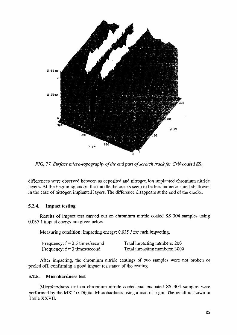
5.08 jun
380
a Jim
x jttn
F/G. 77. Surface micro-topography of the end part of scratch track for CrN coated SS.
differences were observed between as deposited and nitrogen ion implanted chromium nitridelayers. At the beginning and in the middle the cracks seem to be less numerous and shallowerin the case of nitrogen implanted layers. The difference disappears at the end of the cracks.
5.2.4. Impact testing
Results of impact test carried out on chromium nitride coated SS 304 samples using0.035 J impact energy are given below:
Measuring condition: Impacting energy: 0.035 J for each impacting.
Frequency: f = 2.5 times/secondFrequency: f = 3 times/second
Total impacting numbers: 200Total impacting numbers: 3000
After impacting, the chromium nitride coatings of two samples were not broken orpeeled off, confirming a good impact resistance of the coating.
5.2.5. Microhardness test
Microhardness test on chromium nitride coated and uncoated SS 304 samples wereperformed by the MXT-a Digital Microhardness using a load of 5 gm. The result is shown inTable XXVH
85
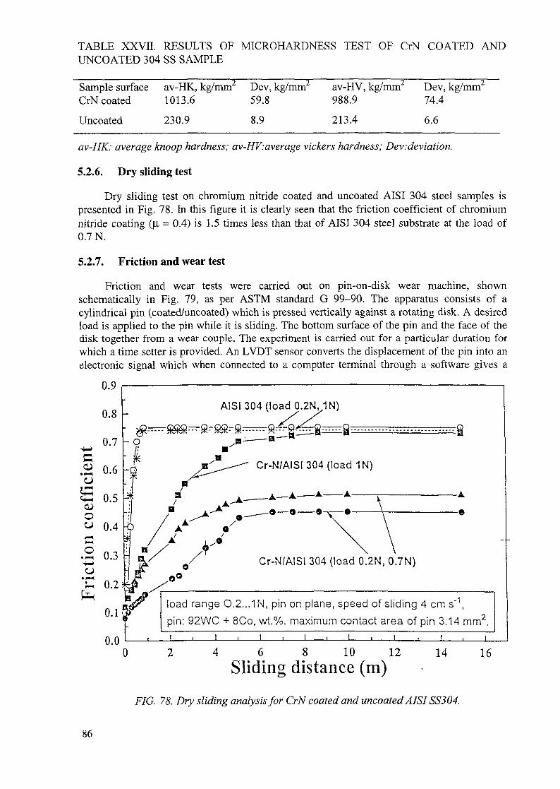
TABLE XXVII. RESULTS OF MICROHARDNESS TEST OF CrN COATED ANDUNCOATED 304 SS SAMPLE
Sample surfaceCrN coated
Uncoated
av-HK, kg/mm1013.6
230.9
Dev, kg/mm2
59.8
8.9
av-HV, kg/mm2
988.9
213.4
Dev, kg/mm74.4
6.6
av-HK: average knoop hardness; av-HV:average vickers hardness; Dev:deviation.
5.2.6. Dry sliding test
Dry sliding test on chromium nitride coated and uncoated AISI 304 steel samples ispresented in Fig. 78. In this figure it is clearly seen that the friction coefficient of chromiumnitride coating (jtt = 0.4) is 1.5 times less than that of AISI 304 steel substrate at the load of0.7 N.
5.2.7. Friction and wear test
Friction and wear tests were carried out on pin-on-disk wear machine, shownschematically in Fig. 79, as per ASTM standard G 99-90. The apparatus consists of acylindrical pin (coated/uncoated) which is pressed vertically against a rotating disk. A desiredload is applied to the pin while it is sliding. The bottom surface of the pin and the face of thedisk together from a wear couple. The experiment is carried out for a particular duration forwhich a time setter is provided. An LVDT sensor converts the displacement of the pin into anelectronic signal which when connected to a computer terminal through a software gives a
AlSi 304 (load 0.2N.1N)
Q-QQ-Q___ Q:rr-Q>^. Q......Q....VIS ST^S**.* xls" -•"-"- yfc~ ^ * ~ " *_, KM ————— 9 ———-————
Cr-N/AIS! 304 (load 1N)
Cr-N/AISl 304 (load 0.2N, 0.7N)
load range O.2...1N, pin on plane, speed of sliding 4 cm s"1,pin: 92WC + 8Co, wt.%. maximum contact area of pin 3.14 mm2.
4 6 8 10 12Sliding distance (m)
14 16
FIG. 78. Dry sliding analysis for CrN coated and uncoated AISISS304.
86
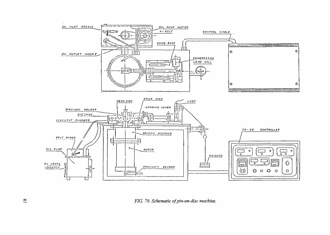
OIL. /SL5T NOZZLE
c/\eif
00 F/G. 79. Schematic ofpin-on-disc machine.
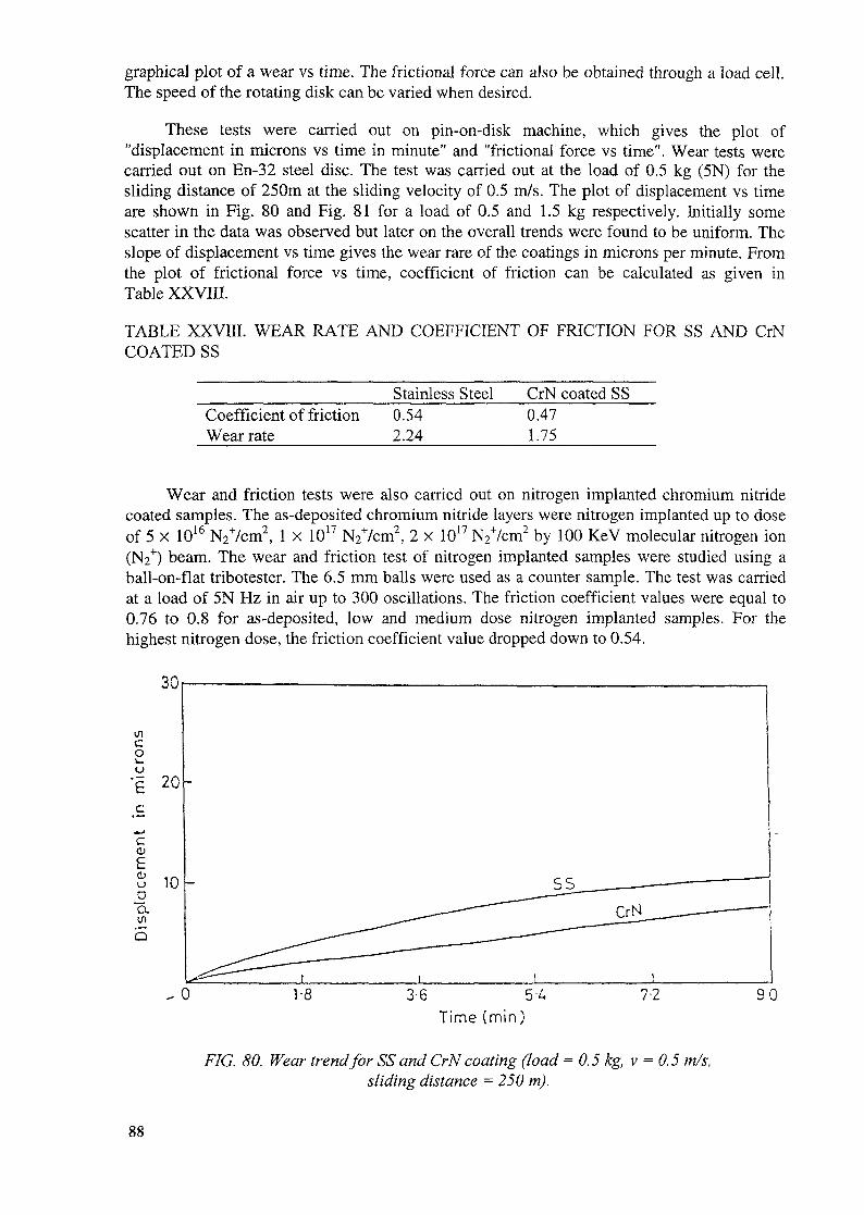
graphical plot of a wear vs time. The frictional force can also be obtained through a load cell.The speed of the rotating disk can be varied when desired.
These tests were carried out on pin-on-disk machine, which gives the plot of"displacement in microns vs time in minute" and "frictional force vs time". Wear tests werecarried out on En-32 steel disc. The test was carried out at the load of 0.5 kg (5N) for thesliding distance of 250m at the sliding velocity of 0.5 m/s. The plot of displacement vs timeare shown in Fig. 80 and Fig. 81 for a load of 0.5 and 1.5 kg respectively. Initially somescatter in the data was observed but later on the overall trends were found to be uniform. Theslope of displacement vs time gives the wear rare of the coatings in microns per minute. Fromthe plot of frictional force vs time, coefficient of friction can be calculated as given inTable XXVIII.
TABLE XXVIII. WEAR RATE AND COEFFICIENT OF FRICTION FOR SS AND CrNCOATED SS
Coefficient of frictionWear rate
Stainless Steel0.542.24
CrN coated SS0.471.75
Wear and friction tests were also carried out on nitrogen implanted chromium nitridecoated samples. The as-deposited chromium nitride layers were nitrogen implanted up to doseof 5 x 10¹⁶ N2
+/cm2, 1 x 10¹⁷ N2Vcm2, 2 x 10¹⁷ N2+/cm2 by 100 KeV molecular nitrogen ion
(N2+) beam. The wear and friction test of nitrogen implanted samples were studied using a
ball-on-flat tribotester. The 6.5 mm balls were used as a counter sample. The test was carriedat a load of 5N Hz in air up to 300 oscillations. The friction coefficient values were equal to0.76 to 0.8 for as-deposited, low and medium dose nitrogen implanted samples. For thehighest nitrogen dose, the friction coefficient value dropped down to 0.54.
30
cou.U
'6c
c0;E0)u
_oCLui
20
10 55
„ 0 1-1 3-6 5-ATime ( m i n )
7-2 90
FIG. 80. Wear trend for SS and CrN coating (load = 0.5 kg, v = 0.5 m/s,sliding distance = 250 m).
88
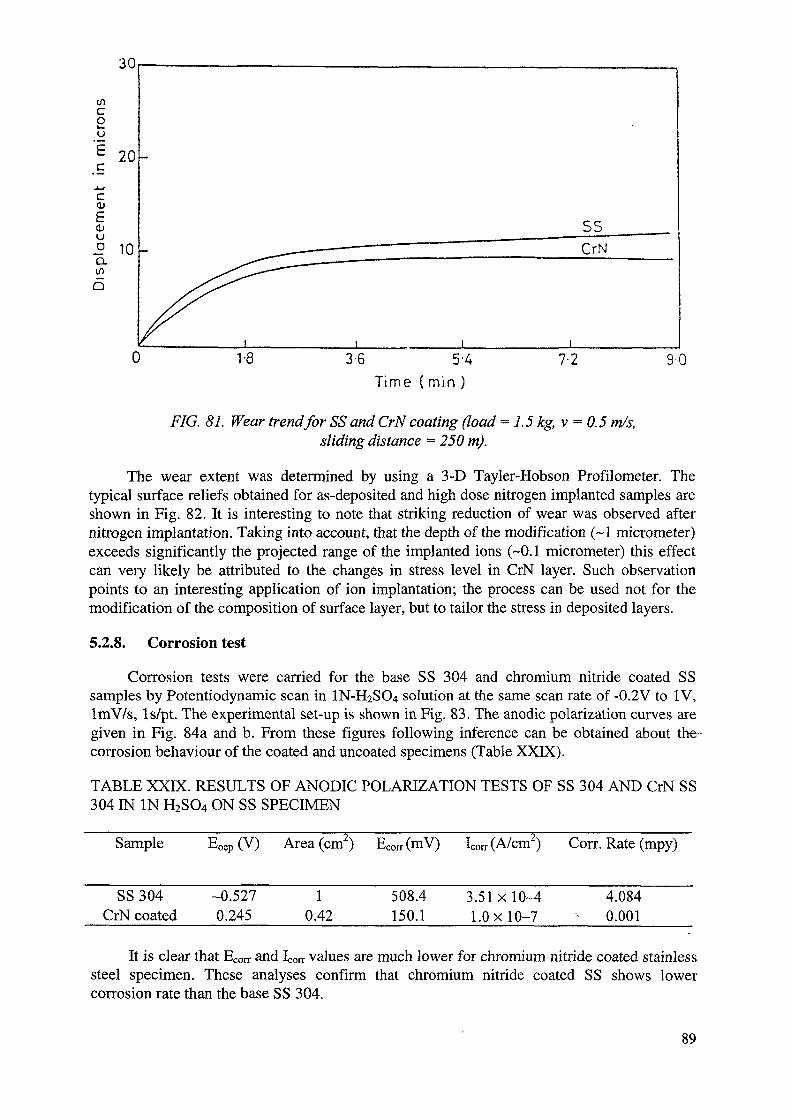
30
tnc
20
c<uediu2 10Q.inQ
0 3-6 5-4Time (min )
7-2 9-0
FIG. 81. Wear trend for SS and CrN coating (load = L5kg,v = 0.5 m/s,sliding distance = 250 m).
The wear extent was determined by using a 3-D Tayler-Hobson Profilometer. Thetypical surface reliefs obtained for as-deposited and high dose nitrogen implanted samples areshown in Fig. 82. It is interesting to note that striking reduction of wear was observed afternitrogen implantation. Taking into account, that the depth of the modification (~1 micrometer)exceeds significantly the projected range of the implanted ions (~0.1 micrometer) this effectcan very likely be attributed to the changes in stress level in CrN layer. Such observationpoints to an interesting application of ion implantation; the process can be used not for themodification of the composition of surface layer, but to tailor the stress in deposited layers.
5.2.8. Corrosion test
Corrosion tests were carried for the base SS 304 and chromium nitride coated SSsamples by Potentiodynamic scan in 1N-H2SO4 solution at the same scan rate of -0.2V to IV,ImV/s, Is/pt. The experimental set-up is shown in Fig. 83. The anodic polarization curves aregiven in Fig. 84a and b. From these figures following inference can be obtained about the-corrosion behaviour of the coated and uncoated specimens (Table XXIX).
TABLE XXIX. RESULTS OF ANODIC POLARIZATION TESTS OF SS 304 AND CrN SS304 IN IN H2SO4 ON SS SPECIMEN
Sample Eocp (V) Area (cm) Ecorr (mV) Icorr (A/cm2) Corr. Rate (mpy)
SS304CrN coated
-0.5270.245
10.42
508.4150.1
3.51x10⁻⁴l.Ox 10-7
4.084- 0.001
It is clear that Ecorr and Icorr values are much lower for chromium nitride coated stainlesssteel specimen. These analyses confirm that chromium nitride coated SS shows lowercorrosion rate than the base SS 304.
89
as-deposited
4.5 jam
-asirrii-?
-3
[4x10¹⁷N/cm2 implanted i «
F/G. 52. Surface profiles using 3-D Tayler-Hobson profilometer for (a) as-deposited(b) nitrogen implanted chromium nitride coated stainless steel.
5.2.9. Discussion
Scanning electron micrographs of chromium nitride coated stainless steel substrateshowed that the chromium nitride coating is uniform and dense. The thickness of thechromium nitride coating on SS specimens was calculated to be 1.3 )im by RBS method,which was also confirmed by Glancing X ray method.
The XPS analysis of the chromium nitride coating on stainless steel sample showed thatthe chromium nitride coating was composed of mostly Cr2N, and potentially CrN in anelemental Cr matrix, and small quantities chromium carbide and oxide. The overall ratio of Cr
90
THERMOMETER.,,
SALT BRIDGE
GAS OUTLET
GAS INLET
REFERENCEELECTRODE
PROBECOUNTERELECTRODE
Y/ORKINGELECTRODE
FIG. 83. Experimental set-tip of Anodic Polarisation.
to N was 75 ± 5% Cr to 25 ± 5% N. This result was further confirmed by AES depth profile ofthe coating, which showed the presence of chromium nitride in the entire coating depth. BothXPS and AES results showed that the chromium nitride coating is a complicated mixture ofCrN, CraN, and chromium oxide. The AES and XPS sputter depth profile have further shownthat the average atomic composition was close to Cr0.8oN0.20 (also confirmed by RBS method)in the sub-surface region; and close to Cro.73No.27 near the substrate/coating interface. Thecoating also contained small quantities of carbide and oxide. The roughness parameters of thecoated specimens measured with the AFM method are: Ra = 5.91 nm and RMS = 7.53 nm, thesame as the substrate samples. Thus, the coating uniformly covers the substrate. Thechromium nitride coating consists mainly of CraN phase as confirmed by glancing XRDanalysis, with grain size of 5 ± 2 |im. The low grain size is a result of low temperature coatingdeposition process which characterizes the IB AD process.
Stainless steel specimens coated with chromium nitride were also subjected to variousperformance tests. Several mechanical tests were carried out on chromium nitride coated anduncoated AISI 304 steel sample. Chromium nitride coatings are not known for low friction;however, dry sliding wear test showed that the friction coefficient of stainless steel improvesby 1.5 times by chromium nitride coating. Other tests such as hardness, scratch and impactmeasurement also showed significant improvement on tribological properties. The adhesion ofthe coating to the substrate proved to be excellent as tested in various, indent and scratch tests.This is another characteristic of IBAD coatings.
91
-0
-Q800-60
1.000
0.200
0.100
O.OQO-10.0
-50 -40 -3.0
Log Current Density (A/cm2)
-ZO
-a.o -6.0 -4.0Log Current Density (A/cm2)
-ZO
FIG. 84. Anodic Polarisation curve of (a) SS 304 (b) CrN coated SS.
6. COST ANALYSIS FOR ION BEAM MODIFICATION PROCESSES
The capital equipment cost for ion implantation system varies depending onspecifications. Mass analyzed ion implanters are significantly more expensive but provide theopportunity to work with a pure elemental species and furthermore with a specific isotope ofthe element. Non-mass-analyzed ion implanters are less expensive and yet quite useful for ionimplantation of gaseous species.
92
Combining ion implantation technology with a coating process adds significantly to thecapital equipment cost but also considerably adds to the performance capability of the system.
A typical cost of ion beam treatment (with the associated equipment requirements suchas transformers, chillers, air conditioning, etc.) system is about US$ 500 000. Pre-owned ionimplanters (from semiconductor manufacturers) can be obtained at a substantially lower cost.(US$ 100 000). New ion implantation systems are considerably more costly (US$ 2 000 000).Unit cost for the ion beam processing of samples is a variable depending on local labour,utility and amortization costs for the equipment. According to recent estimates this cost canvary between US$ 0.1 to 1.0 per cm2 for most typical components processed.
According to the Thai experience the capital cost to set up ion beam based laboratory indeveloping country is:
150 kV mass ion implanter (research type, second hand) US$ 150 000Sample preparation equipment US$ 50 000(polishing machine, profilometer) and test equipment(wear, microhardness)250 m2 laboratory with cooling water and air conditioned US$100 000small housingTotal: US$300 000
The characterization equipment such as a small tandem accelerator, AES, SEM, XRD tostudy depth profiling and surface micrography should be carried in other collaboratinglaboratory. These characterization facilities cost as much as the capital of the whole ion beamlaboratory.
7. CONCLUSIONS
(a) Reliability and reproduction of ion beam technologies make them highly desirable formaterial modification in many industrial applications.
(b) The CRP was able to evaluate alternative ion beam based coating techniques to coatrelatively thicker coatings and achieve improvement in tribological and chemicalproperties of the surfaces.
(c) The main contribution of ion beam techniques is to improve the adhesion of coating tothe substrate. Additional advantage of ion beams is to control the stress in the coatedfilms.
(d) Nitrided coatings achieved by IB AD process (in the range of 1 um) improvedconsiderably wear, friction, hardness, corrosion and oxidation of stainless steel.
(e) CrN coating by plasma arc process, plasma nitriding and Al deposition by ion beammixing process on Ti-Al intermetallics enhanced their high temperature oxidationresistance.
(f) Zr and C deposition by arc vapour deposition improved significantly the hardness andresistance of high speed steels. Also, pre-implantation of Ar followed by TiN coatingsdeposition on steel by arc vapor further enhanced the adhesion of the improved frictionproperties.
(g) W coatings made by ion beam mixing techniques improved the wear and friction of highspeed steel by a factor of four,
(h) Performance of bio-medical implants has been improved by ion beam treatment of lightions such as N and C ions.
93

(i) Ion implantation applied as a post treatment to EBAD coatings and hard Cr platingfurther improve tribiological properties significantly.
(j) Metallic ion implantation (Mo, Y) on SisN4 and ZrOi ceramics by MEVVA enhancedthe conductivity and mechanical properties.
(k) The interlaboratory test carried out by all the participants of CRP, characterized andevaluated the performance of CrN coatings on stainless steel samples. The high-qualitycontribution from each laboratory enhanced the understanding of the properties of thecoating. Coatings like the one evaluated have provided significant potential to improvefriction, wear and corrosion of industrial component.
8. RECOMMENDATIONS
The CRP recognizes the importance of the ion beam based processes as a means forevaluation of surface related properties such as friction, wear, corrosion. Thistechnology offers an excellent opportunity for infrastructure development, training andmutual collaboration among various groups, disciplines and laboratories for furtheradvancement in the understanding of surface related phenomena. The CRP believes thatfor the immediate future these technologies need to be further developed in research andeducational institutions in collaboration with relevant industries.For developing countries with manufacturing industries, an ion beam based techniqueshould be established step by step in order to enhance infrastructure development andfinally finding its own niche market. The establishment of the ion beam laboratory couldbe accomplished in consulting with the Agency through expert groups.For specific niche market, judicious choice should be made for the implementation ofthe available technologies for a specific industrial application.The CRP believes an extension of these technologies to the surface treatment ofpolymers deserves special attention as addition of surface related technologies allowsproperty changes that were not available as conventional technologies such as:
surface cleanliness to improve adherence,electrical properties,surface energy,surface chemistry and structure,mechanical properties,gas permeability.
These technologies offer significant improvement in surface properties of polymers usedin medical application. These property evaluation needs further studies through a wellfocussed CRP.
94
REFERENCES
[I] MARKWITZ, A., et al., Investigation of ultra thin silicon nitride layers produced bylow-energy ion implantation and EB-RTA, Nucl. Instrum. Methods in Phys. Res.,Section B, Beam Interactions with Materials and Atoms 89 1-4 (1994) 362-368.
[2] KETZER, C.S., et al., Synthesis of iron silicides starting with Fe/Si multilayers,Hyperfine Interactions 83 1-4 (1994) 321-325.
[3] LATUSZYNSKI, A., MACZKA, D., Application of radioactive ion beams in the studyof implanted layers, Nucl. Instrum. Methods in Phys. Res., Section B, BeamInteractions with Materials and Atoms (1994) 85 (1-4) 798-802.
[4] ZHANG, T., et al., A study of pulsed high flux Ti, Mo, V, and Y ion implantation forsurface modification of resistances in wear, corrosion and oxidation, Vacuum 45 9(1994)945-950.
[5] SVORCIK, V., et al., Modification of polyethyleneterephtalate by implantation ofnitrogen ions, J. Electrochem. Soc. 141 2 (1994) 582-584.
[6] ITOH, M., et al., Transport properties of modulation-doped grown by molecular beamepitaxy after focused ion beam implantation, Japan. J. Applied Phys., Part 1, RegularPapers and Short Notes 33 IB (1994) 771-774.
[7] POULSEN, J.R., et al., Diffusion of nanaosized sodium inclusions in platinum, J.Phys. Condensed Matter 6 28 (1994) 5397-5408.
[8] POULSEN, J.R., et al., Diffusion of nanaosized sodium inclusions in platinum, J.Phys., Condensed Matter 6 28 (1994) 5397-5408.
[9] ZHANG, J., et al., Ion beam mixing of Ti/Mo bilayers and multilayers, Atom. EnergyScience and Technol. 27 6 (1993) 481-487.
[10] CHEN, M., et al., Ion beam applications on a 100 keV EMIS and ion implanter, TrendsNucl. Phys. 10 4 (1993) 39-42.
[II] SAKAMOTO, K., Modification of polymers with carbon-carbon chain by ionimplantation, IONICS 20 3 (1994) 19-26.
[12] SUZUKI, Y., et al., Ion implantation into polymeric materials for biomedicalapplication, IONICS 20 3 (1994) 35-42.
[13] SUGIZAKI, Y., et al., Effect of ion beam modification on hydrogen absorption bymetals, Surface and Coatings Technol. 65 1-3 (1994) 40-44.
[14] LI, H., JI, C., Surface modification of non-semiconductors by ion beams in China,Surface and Coatings Technol. 65 1-3 (1994) 189-193.
[15] CHEN, J., QIU, H., SHU, C., A 100 keV ion implantation and mixing machine formetal surface modification, Nuclear Techniques 17 1 (1994) 37^1.
[16] RIVIERE, J.P., Surface treatments using ion beams, Materials Science Foruml63-1652(1994)431-448.
[17] NISHIMURA, O., et al., Surface structure of nitrogen ion implanted 304 stainless steel,Surface and Coatings Technol. 66 1-3 (1994) 403-407.
[18] ZHANG, Q.Y., et al., Investigation of TaN films implanted with nitrogen and argonions, Surface and Coatings Technol. 66 1-3 (1994) 468-471.
[19] LIU, L.J., et al., Modification of tribological properties of commercial TiN coatings bycarbon ion implantation, Surface and Coatings Technol. 71 2 (1995) 159-166.
[20] ZHANG, H., et al., Metal ion implantation with three beams, Surface and CoatingsTechnol. 66 1-3 (1994) 345-349.
[21] MULLER, H.R., ENSINGER, W., FRECH, G., WOLF, O.K., A new approach to ionbeam modification of powders (Au/Al_2O_3), Nuclear Instrum. and Meth. Phys. Res.,Section B, Beam Interactions with Materials and Atoms 89 1-4 (1994) 357-361.
95

[22] EVANS, P.J., et al., Surface modification of austenitic stainless steel by titanium ionimplantation, Surface and Coatings Technol. 71 1-3 (1995) 151-158.
[23] BRUEHL, S., et al., Generation of residual deformations by pulsed ion implantation, J.Phys., D, Applied Physics 28 8 (1995) 1655-1660.
[24] SIMSON, S., HEEDE, N., SCHULTZ, J.W., Surface analytical investigations of Al and(Ti, Al) nitrides formed by ion implantation and their corrosion properties, Surface andInterface Anal. 22 1-12 (1994) 431-435.
[25] WOOD, B.P., et al., Initial operation of a large scale plasma source ion implantationexperiment, J. Vacuum Science and Technol. B, Microelectronics 12 2 (1994) 870-874.
[26] AGGARWAL, S., et al., Surface characterization of nitrogen ion implanted etched andpolished AISI 316 stainless steel, Thin Solid Films 237 1-2 (1994) 175-180.
[27] LffiB, K.P., BOLSE, W., UHRMACHER, M., Ion beam mixing in metal/metal andnitride/metal layers-new perspectives, Nuclear Instrum. Methods Phys. Res. Section B,Beam Interactions with Materials and Atoms 89 1-4 (1994) 277-289.
[28] HUANG, C.-T., DUH, J.-G., Nitrogen implantation of Ti and Ti+Al films deposited ontool steel, Vacuum Nucl. Instrum. Methods Phys. Res., Section B, Beam Interactionswith Materials and Atoms 89 1-4 (1994) 369-372.
[29] JIMENEZ-MORALES, A., et al., Electrochemical study of the corrosion behaviour ofcopper surface modified by nitrogen ion implantation, J. Appl. Electrochem., 27 5(1997) 550-557.
[30] CHOI, B.H., et al., The characteristics of surface oxidation and corrosion resistance ofnitrogen implanted zircaloy-4, Surface and Coatings Technol. 89 3 (1997) 252-257.
[31] WANG, X., et al., A study of corrosion resistance behaviour of W+C dual ionimplantated HI3 steel, Nuclear Techniques 20 3 (1997) 138-142.
[32] RAO, Z., SOOD, D.K., WILLIAMS, J.S., O'CONNOR, B.H., Wear behaviour ofcarbon implanted hard chromium coatings, Surface Engineering 13 1 (1997) 61-65.
[33] ENDRST, R., SVORCIK, V., RYBKA, V., Surface modification of polymers inducedby ion implantation, Radiation Effects and Defects in Solids 137 1^ (1995) 25-28.
[34] WANG, G., HA, H., Surface modification of biomaterials with ion implantation inpolymer, J. Isotopes 9 1-4 (1996) 189-192.
[35] HAMPIKIN, J.M., SAQIB, M., POTTER, D.I., Improved oxidation resistance of groupVB refractory metals by Al"+ ion implantation, Metallurgical Transactions, B, ProcessMetallurgy 27 3 (1996) 491-500.
[36] BAI, X.D., ZHU, D.H., LIU, B.X., Anodic and air oxidation of niobium studied by ionbeam analysis with implanted Xe marker, Nuclear Instrum. Methods Phys. Res.Section B, Beam Interactions with Materials and Atoms 114 1-2 (1996) 64-69.
[37] WANG, B., A comparative test for wear resistance of N+ ion implanted piston ringSrNuclear Techniques 19 4 (1996) 208-210.
[38] KNIGHT, S.T., SAMANDI, M., EVANS, P.J., Titanium aluminide formation by ionimplantation, J. Mater, Science Lett. 15 5 (1996) 414^415.
[39] WANG, Q., YANG, X., WANG, Z., Surface modification of alumina by nitrogen ionimplantation, Nuclear Techniques 19 2 (1996) 75-79.
[40] BOUDOUKHA, L., et al., Mechanical characterization by nanaoindentation ofzirconium ion implanted alumina, Nuclear Instrum. Methods Phys. Res., Section B,Beam Interactions with Materials and Atoms 108 1-2 (1996) 87-93.
[41] SHRIVASTAVA, S., et al., Hardening of steel by boron steel ion implantation —dependence on phase composition, Vacuum 47 3 (1996) 247-249.
[42] MITSUO, A., et al., Improvement of thermal oxidation property of thermocouple byAl-ion implantation, IONICS 21 6 (1995) 57-62.
96
[43] KOTHARI, D.C., PRATAP, R., Tribological applications of ion implantation,Transactions of the Metal Finishers' Association of India 4 91 (1995) 67-75.
[44] RUECK, M., DOROTHEE, Experience with the MEW A source for implantingmetals for improved wear, Surface and Coatings Technol. 65 1-3 (1994) 121-127.
[45] ANDERS, A., et al., Metal plasma immersion ion implantation and deposition usingvacuum arc plasma sources, J. Vacuum Science and Technol., B. MicroelectronicsProcessing and Phenomena 12 2 (1994) 815-820.
[46] TUSZEWSKI, M., et al., Plasma immersion ion implantation for semiconductor thinfilm growth, J. Vacuum Science and Technol., B. Microelectronics Processing andPhenomena 12 2 (1994) 973-976.
[47] KOMVOPOULOS, et al., Surface modification of magnetic heads by plasmaimmersion ion implantation and deposition, J. Appl. 76 3 (1994) 1656-1664.
[48] DEB, D., SIAMBIS, J., SYMONS, R., Plasma ion implantation technology for broadindustrial application, J. Vacuum Science Technol., B, Microelectronics Processingand Phenomena 12 2 (1994) 828-832.
[49] ANDERS, A., et. al., Increasing the retained dose by plasma immersion ionimplantation and deposition, Nucl. Instrum. Methods in Phys. Res 102 1-4 (1995),132-135.
[50] ZENG, X., TANG, B., CHU, P.K., Improving the plasma immersion ion implantationimpact energy inside a cylindrical bore by using an auxiliary electrode, Appl. Phys.Lett. 69 25 (1996) 815-3817.
[51] LEE, S.C., HO, W.Y., HUANG, C.C., MELETIS, E.I., LIU, Y., Hydrogenembrittlement and fracture toughness of a titanium alloy with surface modification byhard coatings, J. Mat. Eng. Performance 5 1 (1996) 64-70.
[52] YU, G., GENG, M., HUANG, Y., GONG, X., YU, Y. TANG, D., Application ofMEVVA discharge to material surface modification, Nucl. Fusion Plasma Phys. 16 1(1996)31-35.
[53] THOMAE, R.W., et al., High current ion implantation by plasma immersion technique,Nucl. Instrum. Methods Phys. Res., Section B, Beam Interactions with Materials andAtoms 99 1-4 (1995) 569-572.
[54] BERTOTI, I., MOHAI, M., SULLIVAN, J.L., SAffiD, S.O., Surface chemical changesin PVD TiN layers induced by ion bombardment, Surface and Interface Analysis 21 6-7 (1994) 467-473.
[55] HUSEIN, I.F., ZHOU, Y., QIN, S. CHAN, C., Surface modification by ion and ionbeam implantation, Surface Engineering 13 1 (1997) 56-60.
[56] BOUCHIER, D., et al., Effect of noble gas ions on the synthesis of c-BN by ion beam-assisted deposition, Nucl. Instrum. Methods Phys. Res., Section B, Beam Interactionswith Materials and Atoms 89 1-4 (1994) 369-372
[57] BABA, K., HATADA, R., Corrosion resistant titanium nitride coatings formed onstainless steel by ion beam assisted deposition, Surface and Coatings Technol. 66 1-3(1996) 368-372.
[58] CHUBACI, J.F.D., et al., Formation of carbon nitride — a novel hard coating, Nucl.Instrum. Methods Phys. Res., Section B, Beam Interactions with Materials and Atoms116 1-4(1996)452-456.
[59] CHEN, Z., et al., Surface engineering of steels by plasma immersion ion implantationand related innovative techniques, Surface Engineering 12 2 (1996) 137-141.
[60] ONATE, J.I., et al., Current status of commercial ion implantation in Spain, Surfaceand Coatings Technol. 103-104 (1998) 185-190.
97
[61] ONATE, J.I., et al., Improvement of tribological properties by ion implantation, ThinSolid Films 317 (1998) 471-476.
[62] XIANG, J., HE, S-Z, YANG, K.T, and YUDIAN, R, Formation of A1N films by Alevaporation with nitrogen ion beam bombardment, Mater. Chem. Phys. 51 (1997) 199.
[63] JIANG, Y., ZHANG, H., LIU, C., YANG; S.Z., Novel instrument for material surfacetreatment by pulsed high power density plasma beam; Review Scientific Instrum. 68(1997)4221.
[64] HE, X.J., YANG, S.Z., TAO, K., FAN; Y.D., Reaction of thin metal films with A1Nsubstrate and relevant thermodynamics; J. Vac. Sci. Technol. A (in press).
[65] WEI, K., WU, X., YANG, S-Z., LI, B., LIU C., Study of pulsed high-energy densityplasma modified 0.45%C steel. Materials Science & Engineering A254 (1998) 129-135.
[66] LIU, B., ZHANG, J., CHENG, H.F., JIANG, Y, REN, Y., YANG, S.-Z., Investigationof titanium coatings on 813 by using pulsed high energy density plasma (PHEDP)gun, Materials Chem. Physics (in press).
[67] JIZHONG, Z., et al., "Mechanical property changes in silicon nitride by molybdenumion implantation", Functional Materials, Chemical Engineering Press, Beijing (1997),817-819.
[68] GUAN, C., et al., "Molybdenum film deposited on silicon nitride by ion beamenhanced deposition", Design and Process Chemical Engineering Press, Beijing (1997)373-376 (in Chinese).
[69] JIZHONG, Z, et al., "Mechanical property change of zirconia implanted by Y ions",High Temperature Coatings III (Proc. Symp. San Diego, 1999).
[70] LIU, B., et al., Investigation of titanium coating on SisNi by using a pulsed high energydensity plasma (PHEDP) gun, Materials Chem. Phys. (in press).
[71] GUAN, C., et al., Surface modification of Si3N4 by Mo and Y ion implantation, ThinSolid Films (in press).
[72] UGLOV, V.V., et al., Surf. & Coat. Tech. 103-104 (1998) 317.[73] UGLOV, V.V., et al., Surf. & Coat. Tech. 93 (1997) 331.[74] UGLOV, V.V., et al., Surf. & Coat. Tech. 92 (1997) 190.[75] UGLOV, V.V., et al., Surf. & Coat. Tech. 97 (1997) 322.[76] KHODASEVICH, V.V., et al., Surf. & Coat. Tech. 98 (1998) 1433.[77] YU, L.D., VILAITHONG, T., SUWANNAKACHORN, D., INTARASIRI, S.,
THONGTEM, S., Ion implantation modification of special steels in Thailand, Nucl.Instrum. Methods B127/128 (1997) 954-960.
[78] YU, L.D., VILAITHONG, T., YOTSOMBAT, B., DAVYDOV, S., THONGTEM, S_RHODES, M.W., INTARASIRI, S., SUWANNAKACHORN, D., "Ion implantationfor surface modification of hardened tool steels" (Proceedings Int. Conf. on SurfaceEngineering, Shanghai, China, 1997).
[79] VILAITHONG, T., YU, L.D., VICHAISIRMONGKOL, P., RUJLFANAGUL, G.,SONKAEW, T., N-ion implantation assisted by preparative and closing implantationfor surface modification of tool steel, Nucl. Instrum. Methods Phys. Res. B 148 (1999)830-835.
[80] VILAITHONG, T., YU, L.D., VICHAISIRMONGKOL, P., RUJIJANAGUL, G.,SONKAEW, T., N- ion implantation assisted by preparative and closing implantationfor surface modification of tool steel, Nucl. Instrum. Methods Phys/Res. B 148 (1999)830-835.
[81] JAGffiLSKI, J., MAREST, G., MONCOFFRE, N., Nucl. Instrum. Meth. Phys. Res. B122 (1997)575.
98
[82] JAGIELSKJ, J., KOPCEWICZ, M., TUROS, A., EICHHORN, F., Nucl. Instrum.Meth. Phys. Res. (1999).
[83] JAGIELSKI, J., et al., Nucl. Instrum. Meth. Phys. Res. (1999).[84] MOZETIE, M., ZALAR, A., DROBNIE, M., Comparison of AES and EXAFS analysis
of thin CuxAly layer on Al substrate, Vacuum 50 (1998) 299-304.[85] MOZETIE, M., ZALAR, A., DROBNIE, M., Self-controlled diffusion of Al in Cu thin
film. Vacuum SO (1998) 1-3.[86] MOZETIE, M., ZALAR, A., AREON, I., PRESEREN, R., Characterization of copper
aluminide thin films, Proc. 34lh Int. Conf. On Microelectronics, Devices and Materials,Rog. Slatina (1998), 343-348.
[87] JAGELSKI, J.. et al., Effect of chromium nitride coaling on the corrosion and warresistance of stainless steel. Appl Surface Science 156 (2000) 47-64.
MEXT PAGE(S)left BLANK
CONTRIBUTORS TO DRAFTINGS AND REVIEW
Jagielski, J.
Khanna, A.S.
Kucinski, J.
Misra, D.S.
Onate, J.I.
Racolta, P.
Sioshansi, P.
Thereska, J.
Tobin, E.
Uglov, V.
Vilaithong, T.
Viviente, J.
Yang, S.
Zalar, A.
Zhang, J.
Institute of Electronic Materials Technology, Poland
Indian Institute of Technology, India
Institute of Atomic Energy, Poland
Indian Institute of Technology, India
Centre Tecnologico Materiales, Spain
National Institute of Physics and Nuclear Engineering, Romania
Radio- Med Corporation, United States of America
International Atomic Energy Agency
SPIRE Corporation, United States of America
Belarussian State University, Belarus
Chiang Mai University, Thailand
Centre Tecnologico Materiales, Spain
Chinese Academy of Sciences, China
Institute of Surface Engineering and Optoelectronics, Slovenia
Tsinghua University, China
101