Embed Size (px)
Citation preview

HAL Id: tel-01629767https://tel.archives-ouvertes.fr/tel-01629767
Submitted on 6 Nov 2017
HAL is a multi-disciplinary open accessarchive for the deposit and dissemination of sci-entific research documents, whether they are pub-lished or not. The documents may come fromteaching and research institutions in France orabroad, or from public or private research centers.
L’archive ouverte pluridisciplinaire HAL, estdestinée au dépôt et à la diffusion de documentsscientifiques de niveau recherche, publiés ou non,émanant des établissements d’enseignement et derecherche français ou étrangers, des laboratoirespublics ou privés.
Supramolecular self-assemblies for plasmonics : abottom-up approach to efficient photonic nanodevices
Sylvain Le Liepvre
To cite this version:Sylvain Le Liepvre. Supramolecular self-assemblies for plasmonics : a bottom-up approach to efficientphotonic nanodevices. Materials Science [cond-mat.mtrl-sci]. Université Paris Saclay (COmUE), 2017.English. �NNT : 2017SACLS330�. �tel-01629767�

Supramolecular self-assemblies for plasmonics : a bottom-up
approach to efficient photonic nanodevices
Thèse de doctorat de l'Université Paris-Saclay préparée au CEA Saclay (SPEC)
École doctorale n°572 Ondes et Matière (EDOM) Spécialité de doctorat: Nanophysique
Thèse présentée et soutenue à Gif-sur-Yvette, le 26 septembre 2017, par
Sylvain Le Liepvre Composition du Jury : Jean-Jacques Greffet Professeur, IOGS Président Nathalie Katsonis Professeur Associé, University of Twente Rapporteur Joël Bellessa Professeur des Universités, Université Lyon 1 Rapporteur Steven de Feyter Professeur, KU Leuven Examinateur Sylvain Barbay Professeur, C2N Examinateur Fabrice Charra CEA, SPEC Directeur de thèse
NN
T :
20
17S
AC
LS3
30

Université Paris-Saclay Espace Technologique / Immeuble Discovery
Route de l’Orme aux Merisiers RD 128 / 91190 Saint-Aubin, France
Contents
Remerciements 5
Introduction 9
1 Supramolecular self-assemblies and optical absorption 13
1.1 PTCDI on graphene . . . . . . . . . . . . . . . . . . . . . . . . . . . . . . . 151.1.1 Scanning tunneling microscopy. . . . . . . . . . . . . . . . . . . . . . 151.1.2 PTCDI-C13 Transmission spectra. . . . . . . . . . . . . . . . . . . . 16
1.2 Intermolecular interactions . . . . . . . . . . . . . . . . . . . . . . . . . . . 191.2.1 Non pertubative multipolar 2D model . . . . . . . . . . . . . . . . . 23
1.3 Graphene-molecule interactions . . . . . . . . . . . . . . . . . . . . . . . . . 241.3.1 Electromagnetic interactions . . . . . . . . . . . . . . . . . . . . . . 241.3.2 Change of molecular conformation . . . . . . . . . . . . . . . . . . . 311.3.3 Electronic interactions . . . . . . . . . . . . . . . . . . . . . . . . . . 31
1.4 Dependence on the intermolecular distance . . . . . . . . . . . . . . . . . . 321.5 Dependence on the molecule-graphene distance . . . . . . . . . . . . . . . . 371.6 PTCDI multilayer thin film . . . . . . . . . . . . . . . . . . . . . . . . . . . 411.7 Conclusion . . . . . . . . . . . . . . . . . . . . . . . . . . . . . . . . . . . . 44
2 Supramolecular self-assemblies and fluorescence 47
2.1 Theoretical considerations . . . . . . . . . . . . . . . . . . . . . . . . . . . . 492.1.1 Relaxation paths . . . . . . . . . . . . . . . . . . . . . . . . . . . . . 492.1.2 Energy transfer mechanisms . . . . . . . . . . . . . . . . . . . . . . . 50
2.2 Janus Tecton on graphene . . . . . . . . . . . . . . . . . . . . . . . . . . . . 512.2.1 PTCDI-JT . . . . . . . . . . . . . . . . . . . . . . . . . . . . . . . . 512.2.2 TBC8-JT . . . . . . . . . . . . . . . . . . . . . . . . . . . . . . . . . 58
2.3 Multilayers of Perylene derivatives . . . . . . . . . . . . . . . . . . . . . . . 592.4 Conclusion . . . . . . . . . . . . . . . . . . . . . . . . . . . . . . . . . . . . 60
3 Vibrations of supramolecular self-assemblies on graphene 63
3.1 Introduction to Raman scattering . . . . . . . . . . . . . . . . . . . . . . . . 653.2 Graphene Raman spectrum . . . . . . . . . . . . . . . . . . . . . . . . . . . 673.3 DFT computations . . . . . . . . . . . . . . . . . . . . . . . . . . . . . . . . 703.4 Resonant self-assembled monolayer on graphene . . . . . . . . . . . . . . . . 723.5 Non-resonant self-assembled monolayer on graphene . . . . . . . . . . . . . 753.6 Conclusion . . . . . . . . . . . . . . . . . . . . . . . . . . . . . . . . . . . . 78
4 Plasmon engineering 79
4.1 Characteristics of plasmon modes . . . . . . . . . . . . . . . . . . . . . . . . 814.1.1 Rabi frequency . . . . . . . . . . . . . . . . . . . . . . . . . . . . . . 814.1.2 Field confinement and propagation length . . . . . . . . . . . . . . . 824.1.3 Quality factor . . . . . . . . . . . . . . . . . . . . . . . . . . . . . . . 83
1

CONTENTS
4.2 Maxwell-Garnett materials . . . . . . . . . . . . . . . . . . . . . . . . . . . 83
4.2.1 Glass inclusions. . . . . . . . . . . . . . . . . . . . . . . . . . . . . . 84
4.2.2 Absorber inclusions. . . . . . . . . . . . . . . . . . . . . . . . . . . . 84
4.2.3 Gain medium inclusions. . . . . . . . . . . . . . . . . . . . . . . . . . 85
4.3 Analysis of SPP dispersion relation . . . . . . . . . . . . . . . . . . . . . . . 88
4.3.1 Numerical dispersion relation. . . . . . . . . . . . . . . . . . . . . . . 88
4.3.2 Experimental dispersion relation . . . . . . . . . . . . . . . . . . . . 90
4.4 High-Q plasmon modes . . . . . . . . . . . . . . . . . . . . . . . . . . . . . 92
4.5 Conclusion . . . . . . . . . . . . . . . . . . . . . . . . . . . . . . . . . . . . 94
5 Strongly coupled self-assembled dyes and plasmons 95
5.1 Anti-crossing in self-assembled PTCDI on gold systems . . . . . . . . . . . 98
5.1.1 Tuning the Rabi frequency . . . . . . . . . . . . . . . . . . . . . . . 98
5.1.2 Experimental evidence of anti-crossing . . . . . . . . . . . . . . . . . 100
5.2 Luminescence of self-assembled PTCDI on gold . . . . . . . . . . . . . . . . 100
5.2.1 Strong coupling and Stokes shift . . . . . . . . . . . . . . . . . . . . 100
5.2.2 Experimental wavevector resolved luminescence spectra . . . . . . . 103
5.3 Conclusion . . . . . . . . . . . . . . . . . . . . . . . . . . . . . . . . . . . . 104
6 Supramolecular self-assemblies for plasmon amplification 107
6.1 Molecular self-assemblies as gain medium . . . . . . . . . . . . . . . . . . . 109
6.1.1 Stimulated emission of plasmons . . . . . . . . . . . . . . . . . . . . 109
6.1.2 Molecular self-assemblies as gain media . . . . . . . . . . . . . . . . 110
6.2 Gain limitations in self-assembled thin films . . . . . . . . . . . . . . . . . . 113
6.2.1 Yield, spectrum and decay dependence on pump power . . . . . . . 114
6.2.2 Time-resolved fluorescence spectra . . . . . . . . . . . . . . . . . . . 115
6.2.3 Electronic transition model . . . . . . . . . . . . . . . . . . . . . . . 116
6.3 Conclusion . . . . . . . . . . . . . . . . . . . . . . . . . . . . . . . . . . . . 119
Summary 121
Synthese 123
A Dipole-field interactions theoretical calculations 125
A.1 Frequency to local electric field shifts relation demonstration . . . . . . . . 125
A.2 Absorption of an oriented dipole monolayer . . . . . . . . . . . . . . . . . . 127
A.2.1 Transverse electric polarization . . . . . . . . . . . . . . . . . . . . . 127
A.2.2 Transverse magnetic polarization . . . . . . . . . . . . . . . . . . . . 128
B Self-assembled systems on graphene absorption spectra 131
B.1 Table of experimental shifts and broadenings . . . . . . . . . . . . . . . . . 131
B.2 Polymers on graphene . . . . . . . . . . . . . . . . . . . . . . . . . . . . . . 132
B.3 Small molecules on graphene . . . . . . . . . . . . . . . . . . . . . . . . . . 135
B.4 Annealing effects on absorption spectra . . . . . . . . . . . . . . . . . . . . 138
B.5 Vibrational spectra . . . . . . . . . . . . . . . . . . . . . . . . . . . . . . . . 139
B.5.1 PTCDI-C13 FTIR spectra . . . . . . . . . . . . . . . . . . . . . . . . 139
B.5.2 Self-assembled TSB on graphene Raman spectra . . . . . . . . . . . 139
B.6 Gold nanoparticles coupled to SAM on the graphene surface . . . . . . . . . 141
2

CONTENTS
C Experimental methods 143
C.1 Materials . . . . . . . . . . . . . . . . . . . . . . . . . . . . . . . . . . . . . 143C.1.1 Graphene . . . . . . . . . . . . . . . . . . . . . . . . . . . . . . . . . 143C.1.2 Perylene derivatives . . . . . . . . . . . . . . . . . . . . . . . . . . . 143
C.2 Deposition techniques . . . . . . . . . . . . . . . . . . . . . . . . . . . . . . 143C.3 STM experiments . . . . . . . . . . . . . . . . . . . . . . . . . . . . . . . . . 144C.4 Optical characterization . . . . . . . . . . . . . . . . . . . . . . . . . . . . . 144
C.4.1 Absorption spectra . . . . . . . . . . . . . . . . . . . . . . . . . . . . 144C.4.2 Fluorescence spectra and lifetimes . . . . . . . . . . . . . . . . . . . 144C.4.3 Raman spectra . . . . . . . . . . . . . . . . . . . . . . . . . . . . . . 144
C.5 Numerical computations . . . . . . . . . . . . . . . . . . . . . . . . . . . . . 144C.5.1 Molecular structure . . . . . . . . . . . . . . . . . . . . . . . . . . . 144C.5.2 DFT Calculations . . . . . . . . . . . . . . . . . . . . . . . . . . . . 144
Bibliography 147
3

CONTENTS
4

Remerciements
Apres ces trois annees passionnantes passees au Laboratoire d’Electronique et de Nanopho-tonique Organique (LEPO), j’aimerai remercier chaleureusement mon directeur de theseFabrice Charra pour sa gentillesse, sa disponibilite, ses observations toujours tres perti-nentes, son aide en toutes circonstances et sa patience pour expliquer clairement les pointsles plus obscurs abordes pendant ce travail de these.
J’ai ete marque pendant cette periode par le cadre tres sympathique du laboratoire etje voudrais remercier a ce titre tous les membres permanents de l’equipe qui creent cetenvironnement de travail si agreable, autant du point de vue humain que scientifique :Celine Fiorini, Ludovic Douillard, Simon Vassant, Bruno Delomez.
Cette experience n’aurait pas ete la meme sans les bons moments passes avec les non-permanents de l’equipe : Maud Jaouen pour ses conseils en demontage de STM, PatrickHsia et sa science cinematographique, Celine Molinaro et les frites bruxelloises, SarraMitiche et les fleurets anciens, Farid Kameche et ses theories sur les kebabs, MohammedHoussat alias Barack Obama, Lea Constans, Alice Six, Morgan Auffray, Anaıs Gouesmel,Kim Nguyen, Tessnim Sghaier, Yasmine Nahas, Nathalya Kalashnyk, Quanbo Jiang, Mar-tin Melgarejo, Bastien Jouy, Sebastien Jean-Louis, Milino Kerowgodage et Paul Bouteyre.
Je tiens a remercier l’equipe du C2N qui m’a accueilli pour quelques semaines d’experiencesau sein de leur laboratoire, et avec qui il a ete tres agreable de collaborer tout au long decette these: Sylvain Barbay, Alejandro Giacomotti, John Bigeon, Ariel Levenson.
Merci a toutes les personnes ayant collabore aux differents projets de cette these,beaucoup de belles discussions scientifiques ou plus generales ont resulte de ces rencontres.Merci a toute l’equipe de l’UPMC : Andre-Jean Attias, Fabrice Mathevet, David Kreher,Lydia Sosa-Vargas, a Philippe Lang de Jussieu, a Ludovic Tortech, Quentin Arnoux, SylvieMarguet, Vincent Derycke, Thomas Gustavsson et Valentin Maffeis du CEA Saclay ainsique Jean-Paul Hugonin de l’IOGS.
Tout ce travail n’aurait pu voir le jour sans le soutien de mes proches. Pour eviterle cote un peu lourd de l’exercice des remerciements, je ne peux m’empecher de citer legolfeur Greg Norman excellant dans ce registre : ”Je dois beaucoup a mes parents, surtouta ma mere et a mon pere”. Bref merci papa merci maman et merci les frerots d’avoir apprisplein de trucs au petit dernier.
Dans la categorie abnegation, je dois une mention speciale remerciement a ma femmeElise qui a fait et qui fait toujours l’effort de comprendre des parties de plus en plus vastede ce travail de these, meme si les liens avec l’electromenager renove garanti restent quandmeme assez tenus.
Toujours grands seigneurs en termes de conseils avises, constructeurs de l’extreme,aventuriers sans peurs et sans reproches, mais par-dessus-tout, colocs, j’aimerai claquerun tchek reconnaissant aux colocs de l’Hay Simon, Hadrien et Guillaume, et par extensiona toute la famille de la degaine. (Division d’Escalade Giffoise Aerienne Innovante Nova-trice et Engagee). Mention speciale a Goulven pour son caramel. (le plus goutu de toutlanderneau !)
J’allume a cette ligne la flamme du copain non cite dans les remerciements, tragiquesort pour celui qui a tant œuvre pour me soutenir, me distraire, m’essouffler au cours
5

REMERCIEMENTS
de cette these, heros de l’ombre a qui les portes de l’immortalite du papier viennent dese fermer subitement. Puisse cette flamme porter ton ame en souvenir aux generationsfutures.
Sur ce, bouclez vos ceintures, reperez les issues de secours (qui peuvent se situer derrierevous !), PNC aux portes, on va decoller !
6

”Progress is the realisation of Utopias.”
- Oscar Wilde
A Elise
7


Introduction
”There’s plenty of room at the bottom”. Here are the words of Richard Feynman at anAmerican Physical Society meeting at Caltech in 1959, describing its vision of a technologyworking at the ultimate atom scale. This landmark can be considered as the beginning ofthe nanotechnology field which is devoted to the study and the manufacture of structuresranging in size from 1 to 1000 nm. The development of powerful tools such as the scanningtunneling microscope (STM),1 the atomic force microscope (AFM)2 and other scanningprobe microscopes3 in the 80s have fostered research at the nanoscale giving means toobserve and manipulate systems as small as individual atoms.4
Furthermore, the discovery of low-dimensional materials such as fullerene,5 carbonnanotubes,6,7 graphene,8 single layer boron nitride9 has revealed the potential of nanotech-nology for a vast number of fields such as energy (solar cells,10 fuel cells,11 batteries12),information and communications (transistors,13 transparent conducting electrodes,14 op-toelectronics15), medicine (tissue engineering,16 bioimaging,17 drug delivery18), environ-ment (contamination removal,19 pressure sensors,20 molecular sensor21). However, thenanotechnology era is just beginning and important progresses have to be made aiming atthe design of matter at the nanoscale and at the development of practical applications inmost of the fields mentioned above.
Two strategies can be mentioned when trying to miniaturize existing systems. Thetop-down approach pushes the limits of existing tools such as UV lithography or etchingtechniques to form smaller systems. This strategy is for example used by the semiconductorindustry to scale the size of transistors down to ∼ 10 nm today.22
On the other side, the bottom-up approach is an additive technology using small build-ing blocks such as molecules or atoms to create complex nanoscale systems. Supramolec-ular self-assembly is one of the most advanced techniques able to generate periodically-replicated well-ordered molecular architectures with well-controlled geometry. By chemi-cal design of molecular building blocks, their molecular recognition abilities can be finelytuned so as to spontaneously arrange themselves, forming pre-programmed 1D, 2D or 3Dsupramolecular architectures.23,24,25
Various molecular-recognition processes are at the origin of the self-assembly architec-ture, from steric hindrance26 to hydrogen bonding,27 metal coordination28 or interdigita-tion of alkyl chains.29,30,31
The fabrication of such systems is simple and does not require complex tools unliketop-down approaches. The formation of molecular self-assemblies can easily be obtainedby drop casting or by dip coating techniques, which essentially consists in evaporatinga solution containing the molecular building blocks on a targeted substrate. The self-assembly processes can also take place with molecules deposited in ultra-high vacuumenvironments using molecular beam epitaxy techniques to gain control over the formationof the supramolecular self-assembly.
Plasmonics exploits collective oscillation of electrons in metallic structures to confineoptical fields on dimensions much below their wavelength. This offers unique opportuni-ties for subwavelength optical waveguiding and enhancements of light-matter interactionsthrough intense local fields and optical antennas.32 Nanoplasmonics has made major
9
INTRODUCTION
advances thanks to recent developments in nanoscale manufacturing techniques. Thepossible applications of this field in full development cover wide segments of technology:spectroscopy,33 nanophotonics,34,35 biological sensors,36,37 imaging,38 cancer treatment.39
In recent years, the physics and applications of plasmonic waves interacting with quan-tum emitters became a hot topic.40 In particular, the coupling between a highly confinedplasmonic waveguide and an optical gain medium attracted much attention since theprospect of overcoming propagation losses paves the ways to the development of pho-tonic integrated circuits with subwavelength scale working at optical frequencies.41 Fur-thermore, a robust active plasmonics device would find applications in the realization ofphotovoltaic cells and light-emitting diodes,42 biomedical sensors, fluorescent labels andlight-triggered actuators.43
Various gain media have been used to demonstrate Surface Plasmon Amplification byStimulated Emission of Radiation (SPASER) such as semiconductors44 or π-conjugatedmolecules dispersed in a polymer matrix.45
It has been shown that the distance and the orientation between the fluorophores andthe metal surface plays a crucial role on the coupling between the gain medium and theplasmon mode.46 At small distances, Dexter electron exchange quenching of emitter flu-orescence is preponderant and overcompensates plasmonic enhancements. Moreover, theplasmon mode electric field is mainly perpendicular to the metal surface and thus inter-acts more strongly with emitters displaying the same orientation. Therefore, a gain ofcontrol over the hybrid plasmonic-emitter system structure, especially in the positioningof the emitter relatively to the metal surface could lead to a neat increase of the efficiencyof such active plasmonics devices. Finally, the important spatial confinement of the plas-monic mode electromagnetic field requires a high density of photoactive species in the gainmedium to increase the number of emitter interacting with the electromagnetic mode.
Supramolecular self-assembly offers the flexibility to finely tune molecular scale po-sitioning on a targeted substrate through the chemical design of the molecular buildingblocks. the concept of Janus-like 3D molecular tectons introduced few years ago47 could beused to reduce the Dexter quenching of self-assembled π-conjugated molecules on a metal-lic surface. In these systems, molecular building blocks display a dual-functionalizationat two opposite faces linked by a rigid insulating spacer: a pedestal manages the 2Dself-assembly on the substrate whereas a dye group provides the photonic functionality.Therefore, the lateral organization of the self-assembly array is maintained while liftingphotoactive entities by a few angstroms above the substrate surface thanks to the spacergroup. Such Janus tecton approach paves the way for the precise distance and orientationpositioning of a photoactive entity with reference to a substrate surface, potentially a plas-monic waveguiding surface. Furthermore, very high molecular volume or areal densitiescan be reached in supramolecular self-assemblies. Such hybrid systems would significantlyincrease the number of emitters interacting with a confined plasmonic mode.
However, the aggregation of dyes strongly affects their photonics properties. Inter-molecular interactions lead to increasing or decreasing radiative recombination rates aswell as frequency shifts in the absorption and fluorescence spectrum, depending on con-structive or destructive intermolecular interactions. Experimental and theoretical workhave to be done to determine how do supramolecular self-assemblies tune the photonicsproperties of an active layer through the precise design of intermolecular orientation andpositioning.
In this work, we study the photonic properties of self-assembled molecular monolayerson graphene by correlating the self-assembly structure as deduced from scanning tunnelingand atomic force microscopies to photonic properties as analyzed by optical spectroscopymeasurements. We demonstrate the strong-coupling regime between a 3D molecular self-assembly and a propagating plasmon polariton mode, and show that the optical gain in
10
INTRODUCTION
such dense optically active systems saturates at high excitation rate.
• In chapter 1, we study the optical absorption of perylene derivative self-assembledmonolayers on graphene and explore the effect of intermolecular and molecule-graphene interaction on the absorption spectrum of such hybrid systems. An ex-ample of a three-dimensional perylene self-assembly optimized for interacting withpropagating plasmon polariton is also demonstrated.
• Chapter 2 deals with fluorescence of molecular self-assemblies on graphene. Thefirst fluorescent non-covalent functionalization of graphene by a supramolecular self-assembled monolayer is demonstrated using a Janus tecton approach. The fluores-cence signals of three-dimensional supramolecular self-assemblies suitable for inter-acting with propagating plasmon polaritons are studied.
• Vibrational properties of self-assembled monolayers on graphene are explored inchapter 3. We show the appearance of a coupled vibrational mode between adsorbedmolecules and graphene.
• In chapter 4, we study how to engineer plasmonic modes to reduce losses in themetal. We demonstrate an approach to design plasmonics resonators with highquality factors.
• Strong-coupling between a three-dimensional self-assembly and a propagating plas-mon polariton mode is demonstrated in chapter 5. The photonics properties of sucha system are studied through its absorption and emission responses.
• Finally, chapter 6 presents the conditions for amplifying plasmonic systems by com-paring traditional gain media to molecular self-assemblies. The gain limitation ofmolecular self-assembly systems is studied, and important losses due to exciton-exciton recombination are evidenced.
These chapters relate research projects carried out in collaboration with other teamswithout whom this work would not have been possible. Andre-Jean Attias group(UPMC) worked on designing and synthetizing spontaneously assembling moleculesat the graphene surface (chapters 1 and 2), Matthew Williams and David Andrews(Univ. East Anglia) performed DFT calculations to compute Raman spectra inchapter 3, John Bigeon and Sylvain Barbay (C2N) carried out numerical calculationsand experimental characterizations of the plasmonic systems in chapter 5, ValentinMaffeis and Thomas Gustavssonn performed time resolved fluorescent spectra onPTCDI thin films in chapter 6, Philippe Lang (ITODYS) performed IR experiments(Appendix B), Yannick Dappe (CEA/SPEC) performed DFT calculations to com-pute the density of states (DOS) of adsorbed molecules on graphene (Appendix B),Ludovic Tortech (CEA/NIMBE) was of a precious help for the realization of self-assembled thin films by its advice and the lending of its equipment (chapters 1-3 ,5and 6).
11

INTRODUCTION
12

Chapter 1
Supramolecular self-assemblies
and optical absorption
Supramolecular self-assemblies on highly ordered pyrolitic graphite (HOPG) probed by ascanning tunneling microscope (STM). The presence of molecules is indicated by theyellow color in the STM image. Self-assembled molecules: TBC8 (top left, 11 nm x 11nm), TBC8-JT (bottom left, 100 nm x 100 nm), P3HT (top right, 65 nm x 65 nm),
PTCDI-2C6a (bottom right, 45 nm x 45 nm).
Exotic molecular network patterns such as those displayed above can be drawn onvarious surfaces by designing carefully the structure of molecules that will form the self-assembly. When this system consists of self-assembled dye molecules, what color doesit have? Would it be possible to engineer the color of self-assemblies by changing thegeometrical parameters of the 2D molecular network?
13

1. SUPRAMOLECULAR SELF-ASSEMBLIES AND OPTICAL ABSORPTION
Close-packed assemblies of dye molecules exhibit drastically altered photonic propertiesas compared with the isolated or diluted species.48 These changes find their origin innear-field optical interactions between the constituent molecules, as early predicted byMcRay and Kasha.49 A well-known example is the spectral shift induced by the self-association of cyanine dyes in solution.50 Depending on the aggregation pattern of the dyes,either bathochromically shifted J-bands or hypsochromically shifted H-bands are formed,corresponding to collectively excited states and energy bands of delocalized excitons.51,52
The giant transition dipole moments associated with such excitations result in en-hanced optical interactions, e.g., with plasmon resonators in which case a strong-couplingregime can then be reached.53,54 These collective excitations can also lead to remarkablelight emission processes such as superradiance.55
Interactions between a dye and its surroundings at the molecular scale may alsoinduce drastic changes in its photonic properties. Structural planarization of the ad-sorbed molecules,56 or the immersion inside a polarizable medium57 can induce uniformbathochromic shifts of the vibronic bands constituting the absorption spectrum.
Finally, when distances between π-conjugated systems are small enough to permitelectron tunneling, quantum effects can also come into the play, at the origin, for instance,of new intermolecular charge-transfer absorption bands.58,59
Consequently, the fine tuning of molecular-scale organization of condensed dye assem-blies appears critical for the control of photonic properties of matter and possibly for thegeneration of original photonic processes.
An atomically precise positioning of self-associated molecular dyes can be achievedeither in vacuum or at the solution–substrate interface by self-assembly techniques.
A high level of control of the self-assembly geometry is possible by exploiting theinteractions between alkyl side chains and the surface of highly oriented pyrolytic graphite(HOPG),60 beyond H-bond-steered organizations.61 Based on these principles, it hasbeen possible to design molecular building blocks that arrange spontaneously accordingto various predetermined patterns.31
Graphene has focused intensive research in the past 10 years due to its unusuallyhigh electron mobility, atomic thickness, broadband optical absorption, and unique flex-ibility.62,63,64,8 CVD-grown graphene, being easily transferable onto arbitrary substrateswhile preserving high electronic mobilities,65 soon appeared as a tantalizing candidate forvarious applications in photonics,15 such as solar cells,66 high-speed photodetectors,67 lightsources,68 ultrafast lasers,69 and metamaterials.70 However, as a zero-band-gap semimetal,pristine graphene has a narrow range of roles, merely limited to transparent electrodes.Advanced applications require graphene to be synergistically combined with nanomaterialsproviding complementary properties.
Recently, noncovalent functionalization of graphene with organic molecular buildingblocks has appeared as a promising way to modulate its properties in view of functionalapplications. Actually, graphene provides an atomic-scale crystallographic lattice acting asa template guiding supramolecular self-assembly.71 This bottom-up elaboration process,which implies the physisorption onto graphene of mostly planar molecules (tectons), isnow well mastered in view of electronic applications. For example, supramolecular self-assembly on chemical vapor deposition (CVD)-grown graphene was used to dope graphene,and back-gated graphene field-effect transistor (G-FET) devices were obtained.72
Surprisingly, by comparison with electronics, the noncovalent functionalization of grapheneis still in its infancy as concerns applications in photonics. Yet, organic dyes offer a highflexibility in the design of innovative photonic devices. Actually, because of their highoscillator strengths, they can play the role of light harvesters, photon sources, exciton fun-nels, etc., and as such should provide opportunities to enhance or extend the propertiesof graphene toward light-based applications.
14

1. SUPRAMOLECULAR SELF-ASSEMBLIES AND OPTICAL ABSORPTION
Molecular self-assembly techniques on HOPG substrates can be extended to mono-layer CVD graphene as a substrate,73 which offers optical transparency when transferredfrom its native CVD substrate usually copper– onto a transparent one such as quartz orpolyethylene terephthalate (PET). This offers opportunities for advanced optical charac-terizations in a transmission geometry, such as polarized variable-incidence transmissionspectroscopy. In addition, the electrical conductivity of a CVD graphene monolayer issufficiently high to apply scanning tunneling microscopy (STM) and thus determine thestructural data of the molecular assembly with atomic-scale accuracy.
Self-assembly of adsorbed conjugated molecules can influence the electronic propertiesof its substrate. Such a non covalent functionalization is especially suitable in the case ofgraphene because of its “surface only” nature74,75 and has been applied to tailor its bandstructure76 or its work function77,78 with a monolayer of PTCDI and similar molecules,which can be laterally patterned79 or even manipulated at the single-molecule level.80
Through the combination of optical characterizations and structural control of dyeassemblies on CVD graphene, detailed studies about the influence of the dye organizationon photonic properties become feasible.
In the following, we explore how the optical absorption spectrum of a dye can bechanged once self-assembled on a surface or on a three dimensional network.
1.1 PTCDI on graphene
Perylene-3,4,9,10 tetracarboxylic-3,4,9,10-diimide (PTCDI) and its sibling molecule perylene-3,4,9,10-tetracarboxylic dianhydride (PTCDA) have become archetypes for photonic ap-plications of dyes,81 for self-organized adsorption on various atomically flat surfaces,82
and for their combination. Indeed, optical differential reflectance spectroscopy,83 photo-luminescence, or Raman diffraction studies have evidenced optical responses attributedto strong interactions of PTCDA with metal84,85 or semiconductor86 substrates and be-tween neighboring molecules when deposited on a dielectric substrate87,88 or in multilayerstructures.89 The optical effects of interactions between close-packed PTCDA moleculesdeposited on epitaxial graphene have also been observed.90
1.1.1 Scanning tunneling microscopy.
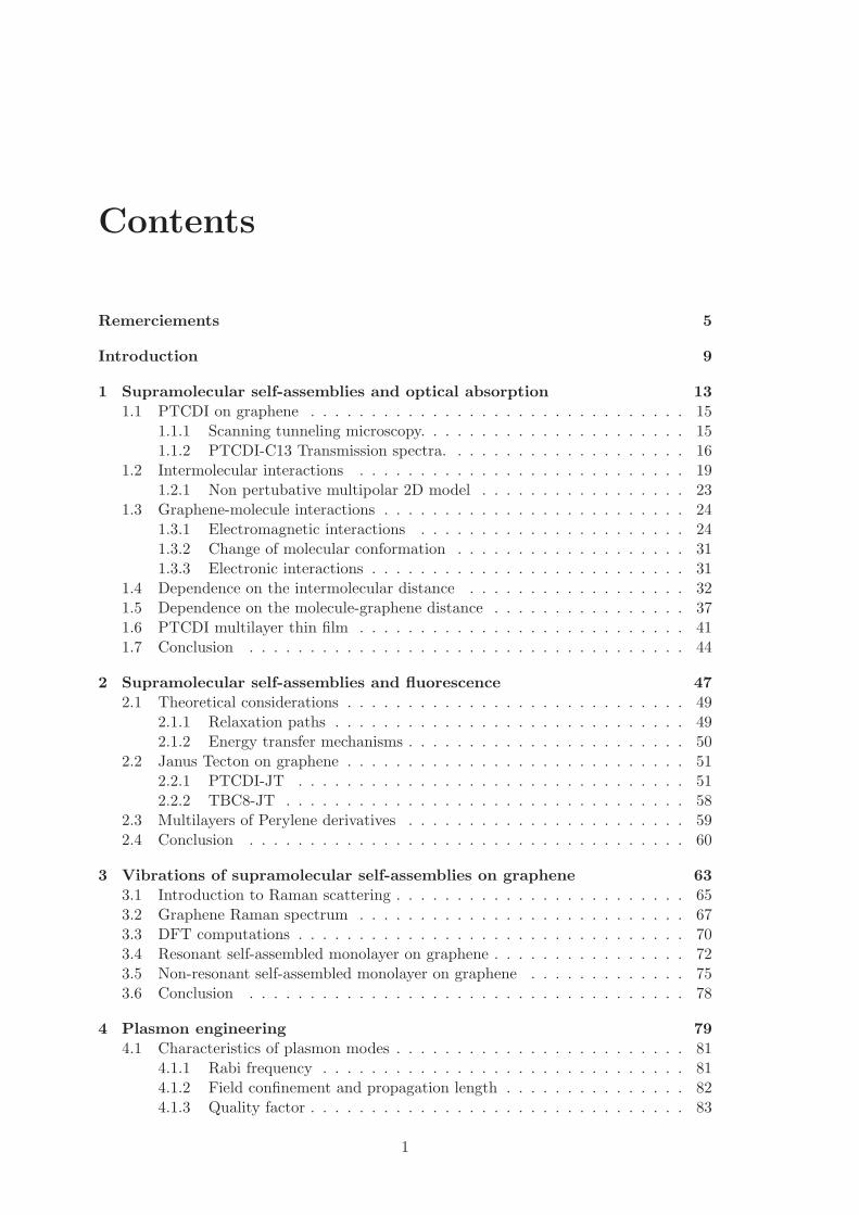
The self-assembly was probed on two graphitic substrates, highly oriented pyrolytic graphite(HOPG) and monolayers of CVD graphene transferred either onto fused silica (“opticalquartz”) or PET. The resolution of carbon atoms is easily obtained on both systems. OnCVD graphene samples, an additional moderate roughness is observed, which is attributedto the substrate (Figure 1.1). For example, in the case of graphene transferred onto afused silica plate, this roughness attains 0.5 nm over distances of approximately 50 nm(Figure 1.1).
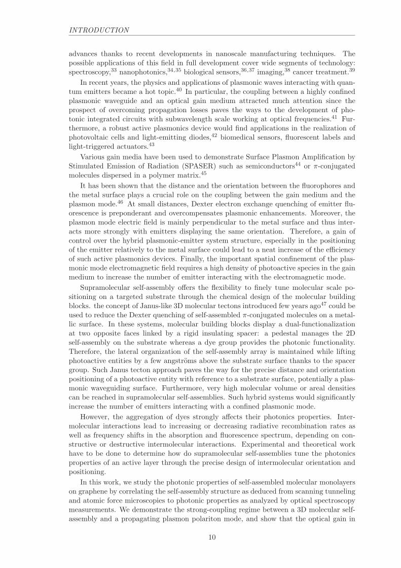
The PTCDI molecule has become a paradigm both as a self-assembly tecton and as adye. For the present study, we chose an alkylated form of this dye, N,N ′−ditridecylperylene−3, 4, 9, 10− tetracarboxylicdiimide (PTCDI-C13), forming a spontaneously self-assembledmonolayer at the interface between the solution and graphene. The monolayer structureshave been studied by STM at the solution–substrate interface.
Figure 1.2 displays STM images of PTCDI-C13 monolayers on HOPG, on as-grownCVD graphene monolayer on copper foil and CVD graphene monolayer transferred ontoPET. The STM technique favors the signature of aromatic skeletons which present higherelectronic surface density of states close to the Fermi level.91
Intramolecular resolution is possible both with HOPG and graphene as substrates(Figure 1.2).
15
1. SUPRAMOLECULAR SELF-ASSEMBLIES AND OPTICAL ABSORPTION
Figure 1.1: Structural characterization of the substrates. STM images (2.3 × 2.3nm2) ofa HOPG surface (a) and CVD monolayer graphene transferred onto a fused quartz plate(b: 2.3× 2.3nm2 and c: 50× 50nm2). The images were acquired under air atmosphere, inthe height (constant current) mode. The setpoint current was IS = 100pA, and the biaswas VT = 200mV . The height scale is also shown for graphene on quartz (c).
Figure 1.2: Structural characterization of the self-assembled PTCDI monolayers. Molec-ular formula of PTCDI-C13 and STM images of self-assembled monolayers on HOPG (a:14×14nm2) as-grown CVD monolayer graphene on copper foil (b: 11×11nm2) and CVDgraphene monolayer transferred onto a PET plate (c: 8 × 8nm2). The typical currentsetpoint and sample bias were 10 pA and 800 mV, respectively. The images were acquiredat the interface between the substrate and a ca. 10−5M solution in phenyloctane at roomtemperature.
As expected from the atomically flat surface of HOPG, this substrate produces thelargest domains. It permits an accurate determination of the lattice parameters, whichcorrespond to a surface density of 0.45 molecules per nm2 and a distance between closestneighbors of ca. 1.4 nm. The network obtained on CVD graphene is compatible withthat obtained on HOPG, with one molecule per unit cell. The various domains have afinite number of lattice orientations, indicating an epitaxial relationship with the graphiticlattice. These results are fully consistent with the expected formation of a self-assembledmonolayer in which the molecules are lying flat on the substrate, with n-alkyl chainsstanding away from the graphene surface due to steric constrains of oxygen atoms.92
By randomly inspecting various regions of drop-cast samples, it appears that a nearlycomplete coverage (about 80%–90%) is obtained whereas the droplet spread on the samplecontained the exact quantity of molecules needed to form a monolayer. The formation ofa second layer is avoided by the presence of alkyl chains standing away from the surfacethat act as a buffer layer.
1.1.2 PTCDI-C13 Transmission spectra.
The solution spectrum of PTCDI-C13 is reported in Figure 1.3 (labelled “SOL”). Itpresents a typical vibronic signature of a π–π∗ transition. Vibronic transitions, involv-
16
1. SUPRAMOLECULAR SELF-ASSEMBLIES AND OPTICAL ABSORPTION
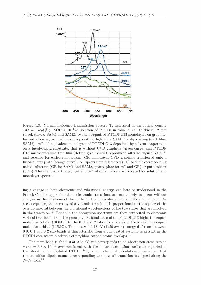
Figure 1.3: Normal incidence transmission spectra T, expressed as an optical densityDO = −log( T
T0). SOL: a 10−6M solution of PTCDI in toluene, cell thickness: 2 mm(black curve). SAM1 and SAM2: two self-organized PTCDI-C13 monolayers on graphite,formed following two methods: drop casting (light blue, SAM1) or dip coating (dark blue,SAM2). µC: 10 equivalent monolayers of PTCDI-C13 deposited by solvent evaporationon a fused-quartz substrate, that is without CVD graphene (green curve) and PTCDI-C13 microcrystalline thin film (dotted green curve) reproduced after Mizuguchi et al.96
and rescaled for easier comparison. GR: monolayer CVD graphene transferred onto afused-quartz plate (orange curve). All spectra are referenced (T0) to their correspondingnaked substrate (GR for SAM1 and SAM2, quartz plate for µC and GR) or pure solvent(SOL). The energies of the 0-0, 0-1 and 0-2 vibronic bands are indicated for solution andmonolayer spectra.
ing a change in both electronic and vibrational energy, can here be understood in theFranck-Condon approximation: electronic transitions are most likely to occur withoutchanges in the positions of the nuclei in the molecular entity and its environment. Asa consequence, the intensity of a vibronic transition is proportional to the square of theoverlap integral between the vibrational wavefunctions of the two states that are involvedin the transition.93 Bands in the absorption spectrum are then attributed to electronicvertical transitions from the ground vibrational state of the PTCDI-C13 highest occupiedmolecular orbital (HOMO) to the 0, 1 and 2 vibrational states of the lowest unoccupiedmolecular orbital (LUMO). The observed 0.18 eV (1450 cm−1) energy difference between0-0, 0-1 and 0-2 sub-bands is characteristic from π-conjugated systems as present in thePTCDI core where p orbitals of neighbor carbon atoms overlaps.94
The main band is the 0–0 at 2.35 eV and corresponds to an absorption cross sectionσSOL = 3.3 × 10⁻¹⁶ cm2 consistent with the molar attenuation coefficient reported inthe literature for alkylated PTCDI.95 Quantum chemical calculations have shown thatthe transition dipole moment corresponding to the π–π∗ transition is aligned along theN–N ′-axis.94
17

1. SUPRAMOLECULAR SELF-ASSEMBLIES AND OPTICAL ABSORPTION
The difference transmission spectra between self-assembled monolayer on a substrateof monolayer CVD graphene transferred onto fused quartz are shown in Figure 1.3. Twotypes of depositions are reported: (i) drop casting of a droplet of a toluene solutioncontaining the exact amount of molecules needed for a coverage of 0.45 molecule per nm2
(SAM 1) and (ii) dipcoating in a ca. 10−5M solution in toluene followed by rinsing intoluene and ethanol (SAM 2).
The transmission spectra of SAM1 and SAM2 are nearly identical and correspond to abathochromic shift of 0.14 eV (1130 cm−1) of the whole vibronic system. This quantitativesimilarity further supports the homogeneous formation of one monolayer by dip coating,as was shown in the case of drop casting. At the maximum of the 0-0 absorption band,shifted to 2.21 eV, the relative transmission ∆T
Tis ca. 2.1% (SAM1) and ca. 1.9% (SAM2).
For an absorbing monolayer deposited on a lossless dielectric substrate, the relativetransmission depends only on the absorptive part of the molecular optical response.97
Given the molecule surface density of 0.45 molecule per nm2 measured by STM, themolecular absorption cross section can be thus evaluated to σML = 4.5 × 10⁻¹⁶ cm2.By assuming an in-plane orientation of the N–N ′-axis, which gives a factor of 3/2 cor-responding to a 2D orientational averaging of the transition dipole moments instead ofthe 3D averaging in solution, the above value is fully consistent with that obtained insolution (3.3×10⁻¹⁶ cm2). Notice that accounting for the Lorentz local field correction to
σSOL, [n2+13
2 1nwith n being the index of refraction of toluene, and for the substrate-index
correction to σML,n+12 with n being the index of the substrate,97 does not change this
conclusion (ca. 1.33 and ca. 1.25, respectively).
Microspectroscopy sampling of the sample, averaged over a spot of about 3µm in di-ameter have shown a high homogeneity of the absorption in the range of millimeters.Remarkably, in the absence of graphene coverage on the fused quartz substrate prior toPTCDI-C13 deposition, completely different transmission spectra are observed. Actu-ally, no measurable absorption is recorded after using the dip coating technique and thespectrum observed for drop casting is very similar to the one reported in the literature forPTCDI microcrystalline films96 (µC, solid and dotted lines). Moreover, microspectroscopyhas shown a high inhomogeneity of the absorption strength, whereas the measured spectraacquired at different places remain homothetic.
Finally, we have measured the dependence on the incidence angle of the PTCDI ab-sorption spectral feature in the polarized absorption for SAM1 and SAM2 samples (Figure1.4). Whereas the absorption increases with incidence for TE polarization (blue trianglesin Figure 1.4), it decreases monotonically with increasing incidence for TM polariza-tion (red squares). In both cases, the molecule spectrum changes homothetically, thatis preserving the balance between vibronic bands. These observations confirm that theorientations of the transition dipole moments of the molecule are parallel to the substratesurface (graphene layer), as shown by the theoretical model98 (continuous lines). This canbe easily seen at grazing incidence where the TM polarized incident electric field is almostperpendicular to the surface, and therefore can’t be absorbed by optical dipoles parallelto the surface. This effect is even visible to the naked eye looking through a tilted platethrough a polarizer. Notice that, for a thin film with random 3D molecule orientation,both TE and TM polarizations should exhibit an increased absorption at grazing incidencebecause the number of molecules illuminated by the incident beam increases.
The quantitative spectral analysis shows that the characteristic optical absorptions ofdrop-cast (SAM1) and dip-coated (SAM2) samples result from a homogeneous assemblyof flat lying molecules with a surface density equivalent to one monolayer. Together withSTM observations, this permits to unambiguously assign the spectral features observedat 2.21, 2.35 and 2.57 eV to the absorption of the PTCDI-C13 monolayer self-assembledonto the graphene substrate with a planar geometry of the molecules.
18

1. SUPRAMOLECULAR SELF-ASSEMBLIES AND OPTICAL ABSORPTION
Figure 1.4: Optical signature of orientations of self-organized PTCDI-C13. Variable-incidence polarized-transmission analysis of the contribution of the self-assembled molecu-lar monolayer to the absorption (blue triangle: TE, red squares: TM). The optical densityat the absorption maximum (λ = 561nm), as obtained from a fit of the absorption lineof the molecule, is plotted. The continuous lines represent the TE and TM theoreti-cal absorption variations98 considering molecular transition dipole moments lying flat ongraphene. For randomly oriented transition dipole moments, both TE and TM shouldincrease with incidence following the blue line.
The most striking feature of the self-assembled monolayer spectra is the uniform red-shift of the whole vibronic spectral line, which results from the self-assembly. This shiftis not accompanied by an important blurring of the spectral structures, consistent withthe high homogeneity of molecular organization and environments obtained through theatomically precise self-assembly process on graphene. The energy difference between 0–0,0–1 and 0–2 sub-bands is preserved, at 0.18 eV. This value is characteristic of the π-conjugated C–C double bond vibration and shows that the absorption remains dominatedby the π–π∗ transition.
2D ordered aggregation of similar molecules on metals have been reported to induceddrastic changes in optical spectra, attributed to new electronic transitions.85 Less pro-nounced rigid spectral shifts have been reported previously for molecules deposited oncrystalline dielectrics such as hexagonal boron nitride (h-BN).56,88 The cited possible ori-gins of such shifts are optical interactions between molecules or between molecules andthe substrate and the deformation of molecules induced by van der Waals interactionsbetween molecules and substrate.
1.2 Intermolecular interactions
Intermolecular optical interactions are a consequence of the local electric field resultingfrom the induced dipoles of molecules at neighboring sites.99 The Coulomb interactionbetween close molecules can result in the creation of a Frenkel exciton, a bound electron-hole pair whose hole is localized at the molecule position.
Intermolecular distances in self-assembled systems are typically on the order of ananometer. Thus, the retarded field can be neglected in the following and all calcula-tions are performed in the quasi-static regime.
19

1. SUPRAMOLECULAR SELF-ASSEMBLIES AND OPTICAL ABSORPTION
The field emitted by a dipole d at a distance r(r, θ) is:
E(r, θ) =1
4πǫr3(3(d.u)u− d) (1.1)
The dipole moment µ for a molecule at a certain frequency ω is related to the excitationlocal electric field through the polarizability α.
µ(ω) = α(ω)Eloc(ω) (1.2)
Since the incident electric field drives the molecular oscillator, all dipole moments in amolecular assembly are coherent in presence of an excitation field, in contrast to the casewhere molecules fluoresce.
In the following, molecules are considered identical and unidimensional. Therefore,the polarizability tensor has only one coefficient. It is possible to model in a classicalpicture (not quantum) the polarizability of the lone molecule applying Newton’s law tothe electron cloud of mass m and charge q represented by its barycenter at position x:
md2x
dt2= FElocal + F tension + F damping (1.3)
The first term represents the Coulombic interaction with the incident electric field, the sec-ond term represents the Coulomb force between the electron cloud and the molecule nuclei(spring force or Hooke’s law) that builds the electronic resonance, the third term repre-sents oscillator losses from which results the quality factor of the resonance. Consideringa sinewave excitation at frequency ω, the above expression can be rewritten:
−ω2mx = qElocal − k(x− x0) + iγ0ωx (1.4)
Multiplying the two parts of equation 1.4 by the charge q, dividing by the mass m andreplacing the dipole moment by its expression µ = qx, we can write:
−ω2µ+ ω0µ− iγωµ =q2Elocal
m(1.5)
The theoretical expression of the polarizability can then be written:
α(ω) =q2/m
ω20 − ω2 − iγω
(1.6)
At resonance, the real part of the polarizability is zero. The imaginary part of thepolarizability can be evaluated through the absorption cross-section σ from:
σ =Im(α0)ω0
3ǫ0c(1.7)
It is experimentally determined by a molar absorptivity ǫ (L × mol−1 × cm−1) mea-surement through:
σ = 1000ln(10)ǫ
NA= ǫ× 3.82× 10⁻²¹ cm2 (1.8)
Where NA is the Avogadro number, ω0 is the resonant frequency, and c the speed oflight.
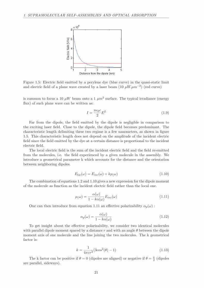
We plot in figure 1.5 the electric field emitted by a perylene dye as a function ofthe distance from this dye in vacuum (n = 1). We use the PTCDI molar absorptivityto compute the polarizability (ǫ = 87000 Lmol−1cm−1). We compare these values tothe incident electric field of a linearly polarized plane wave created by a continuous-wave(CW) laser at the PTCDI resonance wavelength (530 nm). In microscopy experiments, it
20
1. SUPRAMOLECULAR SELF-ASSEMBLIES AND OPTICAL ABSORPTION
Figure 1.5: Electric field emitted by a perylene dye (blue curve) in the quasi-static limitand electric field of a plane wave created by a laser beam (10 µW.µm−2) (red curve)
is common to focus a 10 µW beam onto a 1 µm2 surface. The typical irradiance (energyflux) of such plane wave can be written as:
I =nǫ0c
2E2 (1.9)
Far from the dipole, the field emitted by the dipole is negligible in comparison tothe exciting laser field. Close to the dipole, the dipole field becomes predominant. Thecharacteristic length delimiting these two regime is a few nanometers, as shown in figure1.5. This characteristic length does not depend on the amplitude of the incident electricfield since the field emitted by the dye at a certain distance is proportional to the incidentelectric field.
The local electric field is the sum of the incident electric field and the field re-emittedfrom the molecules, i.e. the field experienced by a given molecule in the assembly. Weintroduce a geometrical parameter k which accounts for the distance and the orientationbetween neighboring dipoles.
Eloc(ω) = Einc(ω) + kµ(ω) (1.10)
The combination of equations 1.2 and 1.10 gives a new expression for the dipole momentof the molecule as function as the incident electric field rather than the local one.
µ(ω) =α(ω)
1− kα(ω)Einc(ω) (1.11)
One can then introduce from equation 1.11 an effective polarizability αp(ω) :
αp(ω) =α(ω)
1− kα(ω)(1.12)
To get insight about the effective polarizability, we consider two identical moleculeswith parallel dipole moment spaced by a distance r and with an angle θ between the dipolemoment axis of one molecule and the line joining the two molecules. The k geometricalfactor is:
k =1
4πεr3(3cos2(θ)− 1) (1.13)
The k factor can be positive if θ = 0 (dipoles are aligned) or negative if θ = π2 (dipoles
are parallel, sideways).
21

1. SUPRAMOLECULAR SELF-ASSEMBLIES AND OPTICAL ABSORPTION
Using the expression of the polarizability developed in equation 1.6, the effectivepolarizability can be rewritten as:
αp(ω) =q2/m
ω20 − kq2
m− ω2 − iγω
(1.14)
Figure 1.6 displays the k geometrical factor in SI units computed for several geometriesof interacting PTCDI and associated imaginary part of the effective polarizability deducedfrom the geometrical factor k and a fit to the polarizability of isolated PTCDI diluted ina toluene solution as described in equation 1.14.
Figure 1.6: Top. Interacting dipoles geometry and associated geometrical factor k in SIunits. To model the PTCDI network on graphene, d = 1.5 nm and θ = 45◦.92 Bottom.Imaginary part of the polarizability for isolated PTCDI when diluted in a toluene solution(black, fit to the experimental data), computed effective polarizabilities for geometricalparameters (SI units) : 1.9× 1036 (blue), −9.4× 1035 (red), 5.3× 1036 (cyan), 1.2× 1037
(green).
A negative k constant (alongside parallel dipole configuration) produces a blue shiftand a lowering of the peak absorption. A positive k constant (aligned dipoles configu-ration or PTCDI 2D network configuration) results in the red shift and an increase ofthe peak absorption. This classical theoretical description is sufficient to retrieve the be-havior of H/J aggregates of the Kasha model.52 The frequency shift is computed to be80 THz = 325 meV when considering an important number of neighbors participatingin the perturbation of the local electric field.
For an assembly of PTCDI-C13 in free space (n = 1), the relative change in localelectric field can be analytically expressed as:
∆E
E=
K
4π
σλ
r3(1.15)
22

1. SUPRAMOLECULAR SELF-ASSEMBLIES AND OPTICAL ABSORPTION
Figure 1.7: LUMO (a) and HOMO (b) of PTCDI-C1. The relaxed geometry has been cal-culated with the constraint DFT at the B3LYP/TZ level. Reproduced from U. Heinemeyeret al.100
where σ is the absorption cross-section (3.3×10⁻¹⁶cm2), λ the excitation wavelength invacuum (ca. 0.5 µm), r the distance between molecules (1.4 nm), and K a factor typicallyof the order of unity. This change in the local electric field in the case of self-assembledPTCDI-C13 is about 50%, which would be more than sufficient to explain the large redshift in the absorption spectrum observed experimentally.
However, this theoretical model does not explain the PTCDI vibronic replicas globalband redshift nor oscillator strength redistribution observed experimentally. A perturba-tion Hamiltonian could then be used to describe electromagnetic interactions between dyesdisplaying virbonic replicas to predict more accurately both the shift and the oscillatorstrength of PTCDI vibronic replicas by considering multiple-particle states.52
A refined model taking into account non perturbative and high order multipolar in-teractions between charges, and the simultaneous interaction with several molecules ofthe 2D network is developed in the following section to attempt to reduce the mismatchbetween the predicted theoretical and experimental frequency shift.
1.2.1 Non pertubative multipolar 2D model
Figure 2.1 represents the wavefunction of the HOMO and LUMO states of a perylenederivative, PTCDI-C1.100 The transition dipole moment is computed by taking the prod-uct of the LUMO and HOMO wavefunctions. As displayed in the figure, charges partici-pating in the dye-light interaction are delocalized over the whole aromatic core of the dyemolecule.
The distance between the two extreme nitrogen atoms of PTCDI is 1.2 nm and roughlycorresponds to the delocalization length of charges through the aromatic core of themolecule. Since self-assembled PTCDI-C13 on graphene are approximately 0.3 nm apart,the dipole approximation that holds for computing electric fields far from an emittingdipole can’t be used.
To develop a simpler classical model to predict the frequency shift of interacting self-assembled dyes, charges representing the transition dipole moment between S0 and S1singlet states will be considered to be localized at the extremities of the dye conjugatedparts. In the following, they are assumed to be 1.2 nm apart, which correspond to theN-N distance in the PTCDI-C13 molecule. This hypothesis is consistent with the Kekuleapproach where charges appear at the extremity of the sp2 conjugated orbitals. Thisconsideration is also consistent with longer conjugation length in dye molecules shiftingresonances to the red. The problem is solved in the quasistatic regime since distances arefar smaller than the wavelength. Typically, the electric field is computed in a 5 nm×5 nmspatial window.
From a spatial charge distribution deduced from a scanning tunneling experiment wecan compute the electric field at every point of the molecular network. We then comparethe local electric field between the two opposite charges representing the molecular dipole
23

1. SUPRAMOLECULAR SELF-ASSEMBLIES AND OPTICAL ABSORPTION
Figure 1.8: Left. 2D charge potential network deduced from PTCDI-C13 on graphenenetwork. Right. Resulting absolute electric field (log scale).
between a lone molecule and an assembly of close molecules. This comparison allows aderivation of the change in the oscillator frequency between the lone molecules and theassembled molecules situations.
ωnetwork
ωalone
=
√
Enetwork
Ealone
(1.16)
Figure 1.8 displays the 2D network of charge potential and the logarithm of the electricfield absolute value resulting from the PTCDI-C13 self-assembly on graphene networkgeometry. We consider only a central molecule and its nearest neighbors. The extensionof the perylene conjugated core is computed to be (5+ 6× 1
2)× 0.15 ≃ 1.2 nm assuminga C-C bond length of 150 pm.
The change in the electric field between the two charges of the central molecule iscomputed to be zero at a charge position and non zero between the two charges. It resultsa frequency shift of the resonance that is comprised between 0 and 115 THz = 480 meVat different location between the two charges. Considering that the overall effect of thelocal electric field on the resonance frequency shift is the mean of every locations betweenthe charges, we compute a frequency shift of 50 THz = 200 meV which is consistentwith the experimental observation (160 meV ).
However, such resonant interactions should also lead to a concentration of the oscillatorstrength on the 0-0 vibronic transition.101 Yet, in the present case, a fit of the absorptionline accounting for the spectral broadening of the vibronic structures gives an increaseof the 0-0 to 0-1 ratio of about 20%, which is not consistent with the 280% value foundcomputing the effective polarizability for a 200 meV frequency shift.
Therefore, the strong resonant molecule–molecule interaction evaluated above in freespace may thus be screened by the presence of the highly polarizable graphene substrate.Graphene-molecule interactions should be explored to understand the role of these inter-actions on the absorption spectrum of self-assembled PTCDI on graphene.
1.3 Graphene-molecule interactions
1.3.1 Electromagnetic interactions
We show hereafter how the strongly increased polarizability of the environment102 of theadsorbed molecules as compared with nearly isolated ones when diluted in toluene solution
24
1. SUPRAMOLECULAR SELF-ASSEMBLIES AND OPTICAL ABSORPTION
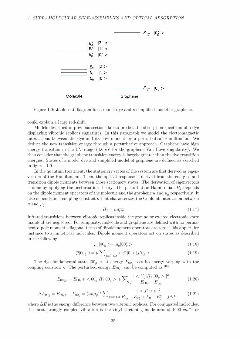
Figure 1.9: Jablonski diagram for a model dye and a simplified model of graphene.
could explain a large red-shift.Models described in previous sections fail to predict the absorption spectrum of a dye
displaying vibronic replicas signatures. In this paragraph we model the electromagneticinteractions between the dye and its environment by a perturbation Hamiltonian. Wededuce the new transition energy through a perturbative approach. Graphene have highenergy transition in the UV range (4.6 eV for the graphene Van Hove singularity). Wethen consider that the graphene transition energy is largely greater than the dye transitionenergies. States of a model dye and simplified model of graphene are defined as sketchedin figure 1.9.
In the quantum treatment, the stationary states of the system are first derived as eigen-vectors of the Hamiltonian. Then, the optical response is derived from the energies andtransition dipole moments between those stationary states. The derivation of eigenvectorsis done by applying the perturbation theory. The perturbation Hamiltonian H1 dependson the dipole moment operators of the molecule and the graphene µ and µg respectively. Italso depends on a coupling constant κ that characterizes the Coulomb interaction betweenµ and µg.
H1 = κµµg (1.17)
Infrared transitions between vibronic replicas inside the ground or excited electronic statemanifold are neglected. For simplicity, molecule and graphene are defined with no perma-nent dipole moment: diagonal terms of dipole moment operators are zero. This applies forinstance to symmetrical molecules. Dipole moment operators act on states as describedin the following:
µg|00g >= µg|00∗g > (1.18)
µ|00g >= µ∑
j=0,1,2< j∗|0 > |j∗0g > (1.19)
The dye fundamental state |00g > at energy E00g sees its energy varying with thecoupling constant κ. The perturbed energy E00gp can be computed as:103
E00gp = E00g+ < 00g|H1|00g > +∑
i,j
| < ijg|H1|00g > |2E00g − Eijg
(1.20)
∆E00g = E00gp − E00g = (κµµg)2∑
j=0,1,2
| < j∗|0 > |2E0g − E0∗g + E0 − E∗
0 − j∆E(1.21)
where ∆E is the energy difference between two vibronic replicas. For conjugated molecules,the most strongly coupled vibration is the vinyl stretching mode around 1600 cm−1 or
25

1. SUPRAMOLECULAR SELF-ASSEMBLIES AND OPTICAL ABSORPTION
180 meV . Since the solvent transition is in the UV range and the dye transition in thevisible range, we neglect this IR transitions for j=0,1,2. We obtain the energy shift forthe |00g > state:
∆E00g =(κµµg)
2
E0g − E0∗g + E0 − E∗0
(1.22)
with the sum rule:∑
j=0,1,2| < j∗|0 > |2 = 1 (1.23)
The first respectively second excited state of the molecule |0∗0g > (resp. |1∗0g >)at energyE0∗0g (resp. E1∗0g) sees its energy perturbed by a factor ∆E0∗0g (resp. ∆E1∗0g):
∆E0∗0g = E0∗0gp − E0∗0g (1.24)
∆E1∗0g = E1∗0gp − E1∗0g (1.25)
∆E0∗0g =(κµµg)
2
E0g − E0∗g + E∗0 − E0
(1.26)
∆E1∗0g = ∆E0∗0g (1.27)
The transition energy shift ∆gap = ∆E0∗0g − ∆E00g induced by the interaction withthe solvent for the dye can then be written:
∆gap =−2(κµµg)
2(E0∗ − E0)
(E0∗g − E0g)2 − (E0∗ − E0)2
(1.28)
This energy shift is identical for the three vibronic replicas. For a positive couplingκ > 0 the shift is negative, meaning that all vibronic replicas absorption bands shifts tothe red.
The transition energy shift can also be computed for the graphene. In this case, thetransition energy shifts to the blue:
∆gap graphene =−2(κµµg)
2(E0∗g − E0g)
(E0∗g − E0g)2 − (E0∗ − E0)2
(1.29)
Note that one can then deduce the solvent shift knowing the dye shift since the ratioof the two shifts only depends on the transitions without any perturbations:
∆gap graphene
∆gap=
E0∗g − E0g
E0∗ − E0(1.30)
This perturbative quantum model can be tested by comparing the graphene transmis-sion spectra with and without PTCDI-C13 self-assembly. The molecule-solvent couplingmodel predicts a blue-shift of the Van Hove singularity once PTCDI-C13 are adsorbed atthe graphene surface. From the PTCDI-C13 on graphene transmission spectrum consid-ering that the red-shift is entirely produced by the PTCDI-C13-graphene interaction, thegraphene Van Hove transition is predicted to shift by:
∆graphene = ∆PTCDI−C13 ×4.6eV
2.3eV= 0.32eV (1.31)
where ∆PTCDI−C13 = 0.16 eV is the shift of PTCDI-C13 absorption bands. Since4.6 eV = 270 nm the transmission spectrum should reveal a shift from 270 nm to252 nm. UV-VIS transmission spectra of graphene on quartz, PTCDI-C13 functionalizedgraphene on quartz, and the quartz substrate are displayed in figure 1.10.
26

1. SUPRAMOLECULAR SELF-ASSEMBLIES AND OPTICAL ABSORPTION
Figure 1.10: Absorption spectra of a reference quartz plate (green curve), graphene onquartz (blue curve) and self-assembled PTCDI-C13 on graphene on quartz (red curve).
The Van Hove singularity is clearly visible at 270nm in the graphene on quartz curve.Its absorption peaks at 9 percent at 270 nm, whereas it converges to 2 percent for visible-IRwavelengths. The functionalization of graphene by the non-covalently bound PTCDI-C13self-assembly produces a clear new band in the UV range at 230nm. This is too farenergetically from the predicted 252 nm to be attributed to a shift of the Van Hove sin-gularity. We explain this new band by the UV absorption of PTCDI-C13 molecule. Aprecise fit on the graphene van Hove band reveals a 10 meV shift that could be the signof the graphene-molecule coupling. It then means that graphene-molecule interactions arenegligible in comparison to intermolecular interactions. However, only couplings betweenmolecular states and van Hove transition states are considered in this model. The con-tribution of all other graphene possible transitions has to be considered to fully representthe interaction between graphene and adsorbed molecule on top of it.
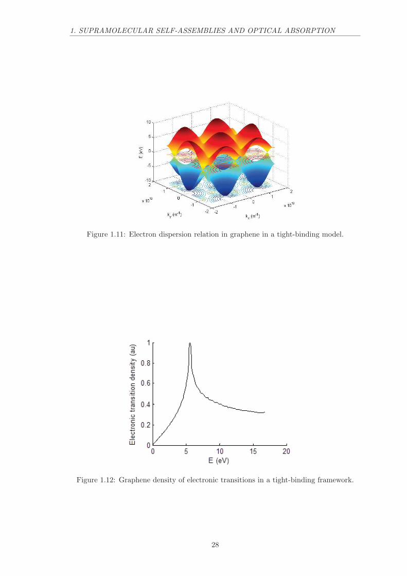
The electronic properties of graphene can be modeled in a tight-binding approach.104
In this framework, graphene electrons energy depends on the wavevector through the 2Ddispersion relation:
E(kx, ky) = ±t√
3 + f − tt× f (1.32)
f = 2cos(a× ky√3) + 4cos(
a× ky√3
2)cos(a× kx
3
2)
where a is the graphene lattice constant (a = 0.24612× 10⁻⁹ m), t is the hopping energy(t = 2.8 eV ) and tt is the nearest neighbor hopping energy (tt = 0.1 eV ). This 2Ddispersion relation is represented in figure 1.11. This dispersion relation displays Diraccones where the electronic density of states is constant and thus where electrons behavelike a 2D electron gaz.
The density of states (DOS) and thus the absorption spectrum of graphene can thenbe computed. Figure 1.12 displays the density of possible electronic transitions thatis closely related to the absorption spectrum. This transition density peaks at 5.6 eVwhereas experimentally the absorption spectrum of graphene peaks at 4.6 eV . This bandis usually referred as the graphene van Hove singularity.
For simplicity purposes the 2D dispersion relation of graphene electrons will be pro-jected on the kx axis in the following. We discretize the dispersion relation of graphene bya orthogonal base of eigenvector states corresponding to k wavevectors. The orthogonalcharacteristic is given by the orthogonality of propagating waves with different wavevec-tors (Fourier decomposition). The state defined by the wavevector k has an energy e(k)defined by the dispersion relation of graphene electrons.
27
1. SUPRAMOLECULAR SELF-ASSEMBLIES AND OPTICAL ABSORPTION
Figure 1.11: Electron dispersion relation in graphene in a tight-binding model.
Figure 1.12: Graphene density of electronic transitions in a tight-binding framework.
28
1. SUPRAMOLECULAR SELF-ASSEMBLIES AND OPTICAL ABSORPTION
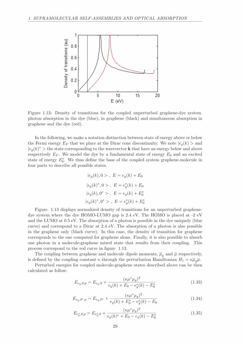
Figure 1.13: Density of transitions for the coupled unperturbed graphene-dye system.photon absorption in the dye (blue), in graphene (black) and simultaneous absorption ingraphene and the dye (red).
In the following, we make a notation distinction between state of energy above or belowthe Fermi energy EF that we place at the Dirac cone discontinuity. We note |eg(k) > and|eg(k)∗ > the state corresponding to the wavevector k that have an energy below and aboverespectively EF . We model the dye by a fundamental state of energy E0 and an excitedstate of energy E∗
0 . We thus define the base of the coupled system graphene-molecule infour parts to describe all possible states.
|eg(k), 0 > , E = eg(k) + E0
|eg(k)∗, 0 > , E = e∗g(k) + E0
|eg(k), 0∗ > , E = eg(k) + E∗0
|eg(k)∗, 0∗ > , E = e∗g(k) + E∗0
Figure 1.13 displays normalized density of transitions for an unperturbed graphene-dye system where the dye HOMO-LUMO gap is 2.4 eV. The HOMO is placed at -2 eVand the LUMO at 0.5 eV. The absorption of a photon is possible in the dye uniquely (bluecurve) and correspond to a Dirac at 2.4 eV. The absorption of a photon is also possiblein the graphene only (black curve). In this case, the density of transition for graphenecorresponds to the one computed for graphene alone. Finally, it is also possible to absorbone photon in a molecule-graphene mixed state that results from their coupling. Thisprocess correspond to the red curve in figure 1.13.
The coupling between graphene and molecule dipole moments, µg and µ respectively,is defined by the coupling constant κ through the perturbation Hamiltonian H1 = κµgµ.
Perturbed energies for coupled molecule-graphene states described above can be thencalculated as follow:
Eeg ,0,p = Eeg ,0 +(κµ∗µg)
2
eg(k) + E0 − e∗g(k)− E∗0
(1.33)
Eeg ,0∗,p = Eeg ,0∗ +(κµ∗µg)
2
eg(k) + E∗0 − e∗g(k)− E0
(1.34)
Ee∗g ,0,p = Ee∗g ,0 +(κµ∗µg)
2
eg(k)∗ + E0 − eg(k)− E∗0
(1.35)
29
1. SUPRAMOLECULAR SELF-ASSEMBLIES AND OPTICAL ABSORPTION
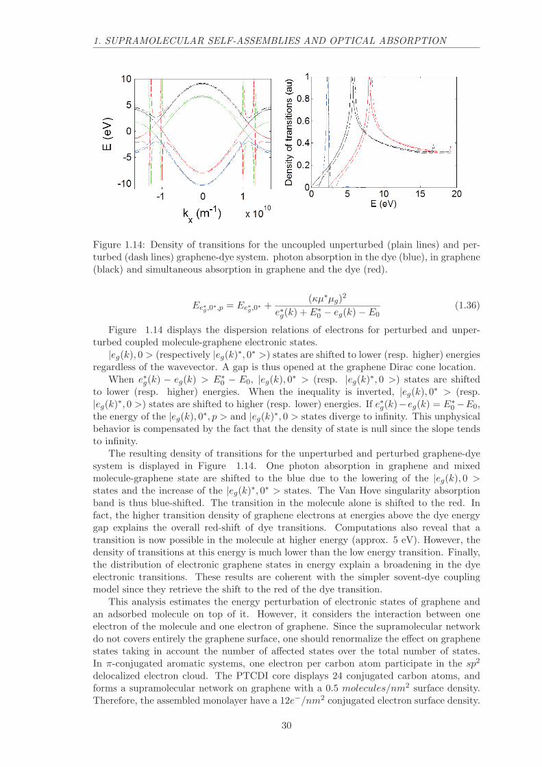
Figure 1.14: Density of transitions for the uncoupled unperturbed (plain lines) and per-turbed (dash lines) graphene-dye system. photon absorption in the dye (blue), in graphene(black) and simultaneous absorption in graphene and the dye (red).
Ee∗g ,0∗,p = Ee∗g ,0
∗ +(κµ∗µg)
2
e∗g(k) + E∗0 − eg(k)− E0
(1.36)
Figure 1.14 displays the dispersion relations of electrons for perturbed and unper-turbed coupled molecule-graphene electronic states.
|eg(k), 0 > (respectively |eg(k)∗, 0∗ >) states are shifted to lower (resp. higher) energiesregardless of the wavevector. A gap is thus opened at the graphene Dirac cone location.
When e∗g(k) − eg(k) > E∗0 − E0, |eg(k), 0∗ > (resp. |eg(k)∗, 0 >) states are shifted
to lower (resp. higher) energies. When the inequality is inverted, |eg(k), 0∗ > (resp.|eg(k)∗, 0 >) states are shifted to higher (resp. lower) energies. If e∗g(k)−eg(k) = E∗
0 −E0,the energy of the |eg(k), 0∗, p > and |eg(k)∗, 0 > states diverge to infinity. This unphysicalbehavior is compensated by the fact that the density of state is null since the slope tendsto infinity.
The resulting density of transitions for the unperturbed and perturbed graphene-dyesystem is displayed in Figure 1.14. One photon absorption in graphene and mixedmolecule-graphene state are shifted to the blue due to the lowering of the |eg(k), 0 >states and the increase of the |eg(k)∗, 0∗ > states. The Van Hove singularity absorptionband is thus blue-shifted. The transition in the molecule alone is shifted to the red. Infact, the higher transition density of graphene electrons at energies above the dye energygap explains the overall red-shift of dye transitions. Computations also reveal that atransition is now possible in the molecule at higher energy (approx. 5 eV). However, thedensity of transitions at this energy is much lower than the low energy transition. Finally,the distribution of electronic graphene states in energy explain a broadening in the dyeelectronic transitions. These results are coherent with the simpler sovent-dye couplingmodel since they retrieve the shift to the red of the dye transition.
This analysis estimates the energy perturbation of electronic states of graphene andan adsorbed molecule on top of it. However, it considers the interaction between oneelectron of the molecule and one electron of graphene. Since the supramolecular networkdo not covers entirely the graphene surface, one should renormalize the effect on graphenestates taking in account the number of affected states over the total number of states.In π-conjugated aromatic systems, one electron per carbon atom participate in the sp2
delocalized electron cloud. The PTCDI core displays 24 conjugated carbon atoms, andforms a supramolecular network on graphene with a 0.5 molecules/nm2 surface density.Therefore, the assembled monolayer have a 12e−/nm2 conjugated electron surface density.
30
1. SUPRAMOLECULAR SELF-ASSEMBLIES AND OPTICAL ABSORPTION
The graphene has two conjugated electrons per unit cell, corresponding to a 39e−/nm2
conjugated electrons surface density. Therefore, only one third of graphene electrons areperturbed as described by this model and the rest of electrons are not affected by thepresence of the supramolecular network.
This model shows that a clear energy shift for all graphene transitions should beproduced by the coupling. Since this energy shift is not observed, we can confidently saythat this coulombic coupling plays a minor role in the photonic properties of self-assembledPTCDI-C13 on graphene.
1.3.2 Change of molecular conformation
The overlapping of neighbor carbon atoms sp2 orbitals in organic molecules allows theformation of a delocalized electron cloud that can be resonant at excitation frequenciesin the visible range. When sp2 orbitals are twisted with reference to each other, theiroverlapping decreases resulting in a shortening of the electron cloud delocalization length.Since the delocalization length determines the resonant frequency of the oscillator, thetwist of sp2 orbitals produce a color shift in the absorption spectrum of the dye molecule.In a classical framework, a capacitance oscillator sees its resonant frequency shifting tothe red when the distance D between charges increases (ω ∼
√D demonstrated previously
in a 1D model). An increase of the electron cloud delocalization length in an organic dyewill shifts its resonance to the red, whereas a decrease of the delocalization length willshifts its resonance to the blue.
Although the interaction between a geometrically complex solvent and an organic dyeis hard to imagine, the interaction between a flat surface (like graphene) and an organicdye is easier. One can expect the flattening of the aromatic dye through the π-π interactionwith the surface. This effect should result in an increase of the delocalization length andthus a red-shift of the dye resonator.
An interesting case is the adsorption of conjugated dyes on carbon nanotubes. In theaxis of the nanotube direction, the delocalization length of the electron cloud should beincreased, like on graphene. However, in the perpendicular axis direction, the curve ofthe nanotube should bends the aromatic dye resulting in a decrease of the electron clouddelocalization length.105
A substrate-induced planarization was invoked for hydrogen bonded porphyrins on h-BN.56 However, the PTCDI molecule already present a rigid intrinsically planar covalentstructure and substrate-induced planarization cannot explain the even larger shift observedhere.
1.3.3 Electronic interactions
Electronic interactions between conjugated π-electron systems of molecule and graphene(π-stacking), as evidenced by STM spectroscopy for non-alkylated PTCDI,80 or by DFTcomputations106 may also play a role in changes of the optical bandgap.
When HOMO and/or LUMO orbitals of a dye are participating in the dye adsorptionprocess to a conductive or semiconductive (including pi-conjugated) substrate, one canexpect a dramatical change in the electronic properties of dye through quantum interac-tions.
The charges can be redistributed between the interacting systems, and new coupledstates can be created such as mixed charge-transfer (CT) and Frenkel excitons with inci-dence on optical properties.
Unlike Frenkel excitons arising from the Coulomb interaction between induced dipolesat molecular sites, charge-transfer excitons result from the overlap of nearest neighbormolecules orbitals wavefunctions. However, at required distances for the CT exciton to
31
1. SUPRAMOLECULAR SELF-ASSEMBLIES AND OPTICAL ABSORPTION
exist (approx. 0.3 nm) the Frenkel exciton is also present resulting in a mixed CT-Frenkelexciton.
For example, the stacking of perylene dyes considerably change the optical absorptionspectrum with the appearance of a new band related to the transition from the S0 vibra-tional ground state to the CT-Frenkel exciton state.107 Such stacking of dye molecules isusually associated with an inhomogeneous broadening of the absorption spectrum sincemultiple stacking conformation are often possible.
The spatial partition of charges is a complex multibody problem defined through theunique structures of each molecule. Density functional theory (DFT) calculations can givean insight into these changes, but at such scale a small distance perturbation producesimportant modifications on electric fields. DFT calculations are then to be taken withprecautions. Hence, the prediction of changes in the absorption spectrum due to chargeredistribution in the dye molecule is a difficult task.
These interpretations are consistent with the observation of a concentration of theoscillator strength for dense assemblies of PTCDA deposited on a dielectric substrate,87
in which case no significant spectral shift was observed.
In summary, we have realized the self-assembly of alkylated PTCDI molecules ontoa monolayer CVD graphene transferred on a transparent substrate. The molecules forma well-organized dense assembly, the parameters of which being accurately determinedby STM. The polarized optical transmission spectra have been acquired at variable inci-dence thanks to the high optical transparency of the monolayer CVD graphene substrate.This confirms that the transition dipoles of adsorbed PTCDI are all oriented parallel tothe substrate. The absorption is consistent with the measured density of molecules andpresents mainly a rigid red-shift of the absorption line compared with the free moleculesdispersed in solution. These changes are attributed to non-resonant interactions with thegraphene layer and the neighboring molecules. The intermolecular coupling results fromthe Coulombic interaction between dipole moments and the graphene-PTCDI-C13 cou-pling from an electronic coupling that modifies the electronic structure of both grapheneand PTCDI-C13.
However, the preservation of the absorption line-shape and the balance between vi-bronic contributions in PTCDI-C13 experimental absorption spectra means that the strongresonant molecule–molecule interaction evaluated in free space is screened by the presenceof the highly polarizable graphene substrate. An exciting perspective could be given byhexagonal boron nitride (h-BN) monolayers, which combine a dielectric nature with anatomic-scale template similar to that of graphene.108
Additional measurements have to be performed on different self-assembled systems tounderstand the contribution of intermolecular and molecule/graphene interactions in themodification of dye photonic properties once adsorbed on the graphene surface. This isthe object of the next section.
1.4 Dependence on the intermolecular distance
To get insight about the origin of the spectral redshift observed for self-assembled dyeson graphene, we made comparisons with other self-assembled dyes on graphene. The twokey physical parameters (intermolecular distance and graphene-molecule distance) shouldbe varied to evaluate the strength of each coupling. However, one should take extra carewhen varying these parameters since they are not fully independent.
A first strategy to modify the 2D supramolecular network could be to change the lengthof alkyl chains which often play a role of spacer between assembled molecules.60,47 Thecontribution to the adsorption force of a ten carbon alkyl chain should not change thatmuch the molecule graphene distance in comparison to a 6 carbon atoms alkyl chain for
32

1. SUPRAMOLECULAR SELF-ASSEMBLIES AND OPTICAL ABSORPTION
Figure 1.15: Normalized transmission absorption spectra of PTCDI-C7 (red), PTCDI-C8 (blue) and PTCDI-C13 (green) diluted in a toluene solution (dark curves) and self-assembled on a graphene on PET surface (light curves).
example.
However, a change in the number of carbon atoms do not have a major impact on thePTCDI-C13 on HOPG supramolecular network, as shown by Ludwig et al.109 PTCDI-C13alkyl chains do not participate in the adsorption force but seem to stand away from thegraphene surface. This conformation originates from the steric constrain produced by theterminal oxygen atoms.
The measured network parameters are a = 1.5 nm, b = 1.7 nm, α = 87.5◦ for PTCDI-C8 and a = 1.6 nm, b = 1.7 nm, α = 88.2◦ for PTCDI-C13. Absorption spectra of PTCDI-C7, PTCDI-C8 and PTCDI-C13 diluted in solution and self-assembled on the graphenesurface are displayed in figure 1.15. The absorption spectra of the three molecules intoluene peak at the same wavelengths. The difference in the distribution of the oscillatorstrength over the vibronic replicas is observed when the concentration of PTCDI dyemolecules is varied. This difference can be attributed to a mismatch between PTCDI-C7,PTCDI-C8 and PTCDI-C13 concentrations during the measurement. The three spectrain solution can therefore be considered as identical, which seems reasonable since a changein the alkyl chain length should not affect the conjugation of perylene core that producethe visible absorption.
As expected from scanning tunneling experiments that show no major changes in the2D molecular network, the absorption spectra of PTCDI-C7, PTCDI-C8 and PTCDI-C13are almost identical once self-assembled on a graphene on PET surface. However, a smallchange in the position of the 0-0 transition is observed between PTCDI-C7 and PTCDI-C8 on one hand and PTCDI-C13 on the other hand. The redshift for PTCDI-C7 andPTCDI-C8 (140 meV ) is slightly smaller than for PTCDI-C13 (155 meV ). Moreover,the absorption peak is slightly smaller for PTCDI-C7 and PTCDI-C8 (2.0%) than forPTCDI-C13 (2.3%). Since the ratio between 0-0 and 0-1 transitions is identical for thethree molecules, the intermolecular interaction should also be identical. This is consistentwith the fact that molecular network geometries are not affected that much by the changein the alkyl length.
The presence of longer alkyl chains changes the dielectric environment around perylenedye dipoles. The refractive index surrounding aromatic cores is increased when alkyl chainsare lengthened from eight to thirteen carbon atoms. The resulting dielectric constant ǫrof the mixture comprising aromatic cores and alkyl chains with respective polarizabilities
33
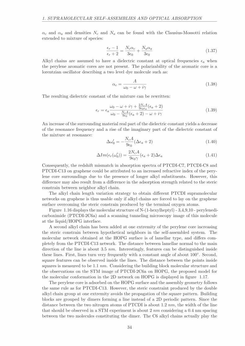
1. SUPRAMOLECULAR SELF-ASSEMBLIES AND OPTICAL ABSORPTION
αc and αa and densities Nc and Na can be found with the Clausius-Mossotti relationextended to mixture of species:
ǫr − 1
ǫr + 2=
Ncαc
3ǫ0+
Naαa
3ǫ0(1.37)
Alkyl chains are assumed to have a dielectric constant at optical frequencies ǫa whenthe perylene aromatic cores are not present. The polarizability of the aromatic core is alorentzian oscillator describing a two level dye molecule such as:
αc =A
ω0 − ω + iγ(1.38)
The resulting dielectric constant of the mixture can be rewritten:
ǫr = ǫaω0 − ω + iγ + 2NcA
9ǫ0ǫa(ǫa + 2)
ω0 − NcA9ǫ0
(ǫa + 2)− ω + iγ(1.39)
An increase of the surrounding material real part of the dielectric constant yields a decreaseof the resonance frequency and a rise of the imaginary part of the dielectric constant ofthe mixture at resonance:
∆ω′0 = −NcA
9ǫ0(∆ǫa + 2) (1.40)
∆Im(ǫr(ω′0)) =
2NcA
9ǫ0γ(ǫa + 2)∆ǫa (1.41)
Consequently, the redshift mismatch in absorption spectra of PTCDI-C7, PTCDI-C8 andPTCDI-C13 on graphene could be attributed to an increased refractive index of the pery-lene core surroundings due to the presence of longer alkyl substituents. However, thisdifference may also result from a difference in the adsorption strength related to the stericconstrain between neighbor alkyl chain.
The alkyl chain length variation strategy to obtain different PTCDI supramolecularnetworks on graphene is thus usable only if alkyl chains are forced to lay on the graphenesurface overcoming the steric constrain produced by the terminal oxygen atoms.
Figure 1.16 displays the molecular structure of N-(1-hexylheptyl) - 3,4,9,10 - perylenedi-carboximide (PTCDI-2C6a) and a scanning tunneling microscopy image of this moleculeat the liquid/HOPG interface.
A second alkyl chain has been added at one extremity of the perylene core increasingthe steric constrain between hypothetical neighbors in the self-assembled system. Themolecular network obtained at the HOPG surface is of lamellar type, and differs com-pletely from the PTCDI-C13 network. The distance between lamellae normal to the maindirection of the line is about 3.5 nm. Interestingly, features can be distinguished insidethese lines. First, lines turn very frequently with a constant angle of about 100◦. Second,square features can be observed inside the lines. The distance between the points insidesquares is measured to be 1.1 nm. Considering the building block molecular structure andthe observations on the STM image of PTCDI-2C6a on HOPG, the proposed model forthe molecular conformation in the 2D network on HOPG is displayed in figure 1.17.
The perylene core is adsorbed on the HOPG surface and the assembly geometry followsthe same rule as for PTCDI-C13. However, the steric constraint produced by the doublealkyl chain group at one extremity avoids the propagation of the square pattern. Buildingblocks are grouped by dimers forming a line instead of a 2D periodic pattern. Since thedistance between the two nitrogen atoms of PTCDI is about 1.2 nm, the width of the linethat should be observed in a STM experiment is about 2 nm considering a 0.4 nm spacingbetween the two molecules constituting the dimer. The C6 alkyl chains actually play the
34

1. SUPRAMOLECULAR SELF-ASSEMBLIES AND OPTICAL ABSORPTION
Figure 1.16: Structural characterization of the self-assembled PTCDI-2C6a monolayer.Left. PTCDI-2C6a molecular structure. Right. STM image of self-assembled monolayeron HOPG (53 nm × 65 nm, 11 pA, 900 mV ), acquired at the interface between thesubstrate and a ca. 10−5 M solution in phenyloctane at room temperature.
Figure 1.17: Model for the self-assembled PTCDI-2C6a monolayer on graphitic surfaces.Color represents the nature of atoms: grey (carbon), blue (nitrogen), red (oxygen), andwhite (hydrogen).
35
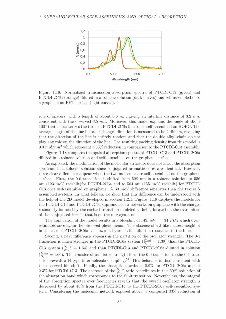
1. SUPRAMOLECULAR SELF-ASSEMBLIES AND OPTICAL ABSORPTION
Figure 1.18: Normalized transmission absorption spectra of PTCDI-C13 (green) andPTCDI-2C6a (orange) diluted in a toluene solution (dark curves) and self-assembled ontoa graphene on PET surface (light curves).
role of spacers, with a length of about 0.6 nm, giving an interline distance of 3.2 nm,consistent with the observed 3.5 nm. Moreover, this model explains the angle of about100◦ that characterizes the turns of PTCDI-2C6a lines once self-assembled on HOPG. Theaverage length of the line before it changes direction is measured to be 2 dimers, revealingthat the direction of the line is entirely random and that the double alkyl chain do notplay any role on the direction of the line. The resulting packing density from this model is0.3 mol/nm2 which represent a 33% reduction in comparison to the PTCDI-C13 assembly.
Figure 1.18 compares the optical absorption spectra of PTCDI-C13 and PTCDI-2C6adiluted in a toluene solution and self-assembled on the graphene surface.
As expected, the modification of the molecular structure does not affect the absorptionspectrum in a toluene solution since conjugated aromatic cores are identical. However,three clear differences appear when the two molecules are self-assembled on the graphenesurface. First, the 0-0 transition is shifted from 528 nm in a toluene solution to 556nm (123 meV redshift)for PTCDI-2C6a and to 564 nm (155 meV redshift) for PTCDI-C13 once self-assembled on graphene. A 30 meV difference separates then the two self-assembled systems. In what follows, we show that this difference can be understood withthe help of the 2D model developed in section 1.2.1. Figure 1.19 displays the models forthe PTCDI-C13 and PTCDI-2C6a supramolecular networks on graphene with the chargesresonantly induced by the excited transition modeled as being located on the extremitiesof the conjugated kernel, that is on the nitrogen atoms.
The application of the model results in a blueshift of 143meV = 34 THz which over-estimates once again the observed phenomenon. The absence of a J-like nearest neighborin the case of PTCDI-2C6a as shown in figure 1.19 shifts the resonance to the blue.
Second, a neat difference appears in the partition of the oscillator strength. The 0-1transition is much stronger in the PTCDI-2C6a system (S0−0
S0−1= 1.39) than the PTCDI-
C13 system (S0−0
S0−1= 1.64) and than PTCDI-C13 and PTCDI-2C6a diluted in solution
(S0−0
S0−1= 1.66). The transfer of oscillator strength form the 0-0 transition to the 0-1 tran-
sition reveals a H-type intermolecular coupling.52 This behavior is thus consistent withthe observed blueshift. Finally, the absorption peaks at 0.9% for PTCDI-2C6a and at2.3% for PTCDI-C13. The decrease of the S0−0
S0−1ratio contributes in this 60% reduction of
the absorption band which corresponds to the S0-0 transition. Nevertheless, the integralof the absorption spectra over frequencies reveals that the overall oscillator strength isdecreased by about 40% from the PTCDI-C13 to the PTCDI-2C6a self-assembled sys-tem. Considering the molecular network exposed above, a computed 33% reduction of
36
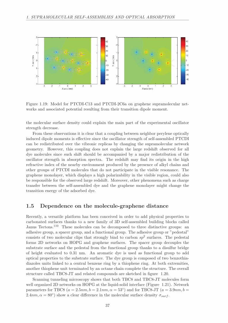
1. SUPRAMOLECULAR SELF-ASSEMBLIES AND OPTICAL ABSORPTION
Figure 1.19: Model for PTCDI-C13 and PTCDI-2C6a on graphene supramolecular net-works and associated potential resulting from their transition dipole moment.
the molecular surface density could explain the main part of the experimental oscillatorstrength decrease.
From these observations it is clear that a coupling between neighbor perylene opticallyinduced dipole moments is effective since the oscillator strength of self-assembled PTCDIcan be redistributed over the vibronic replicas by changing the supramolecular networkgeometry. However, this coupling does not explain the large redshift observed for alldye molecules since such shift should be accompanied by a major redistribution of theoscillator strength in absorption spectra. The redshift may find its origin in the highrefractive index of the nearby environment produced by the presence of alkyl chains andother groups of PTCDI molecules that do not participate in the visible resonance. Thegraphene monolayer, which displays a high polarizability in the visible region, could alsobe responsible for the observed large redshift. Moreover, other phenomena such as chargetransfer between the self-assembled dye and the graphene monolayer might change thetransition energy of the adsorbed dye.
1.5 Dependence on the molecule-graphene distance
Recently, a versatile platform has been conceived in order to add physical properties tocarbonated surfaces thanks to a new family of 3D self-assembled building blocks calledJanus Tectons.110 These molecules can be decomposed to three distinctive groups: anadhesive group, a spacer group, and a functional group. The adhesive group or ”pedestal”consists of two molecular clips that strongly bind to carbon sp2 surfaces. The pedestalforms 2D networks on HOPG and graphene surfaces. The spacer group decouples thesubstrate surface and the pedestal from the functional group thanks to a disulfur bridgeof height evaluated to 0.31 nm. An aromatic dye is used as functional group to addoptical properties to the substrate surface. The dye group is composed of two benzothia-diazoles units linked to a central benzene ring by a thiophene ring. At both extremities,another thiophene unit terminated by an octane chain complete the structure. The overallstructure called TBC8-JT and related compounds are sketched in figure 1.20.
Scanning tunneling microscopy shows that both TBC8 and TBC8-JT molecules formwell organized 2D networks on HOPG at the liquid-solid interface (Figure 1.21). Networkparameters for TBC8 (a = 2.5nm, b = 2.1nm,α = 53◦) and for TBC8-JT (a = 3.9nm, b =2.4nm,α = 80◦) show a clear difference in the molecular surface density σsurf .
37

1. SUPRAMOLECULAR SELF-ASSEMBLIES AND OPTICAL ABSORPTION
Figure 1.20: Schematic structures of the Janus Tecton TBC8-JT, TBC8-JT pedestal andTBC8 molecules.
Figure 1.21: STM images at the liquid/HOPG interface at room temperature: (a) TBC8(11nm× 11nm, It = 90pA, Vt = −460mV ); (b) TBC8-JT (51nm× 54nm, It = 9pA, Vt =−1320mV ); (c) model for the TBC8-JT supramolecular network on HOPG geometry,reproduced from ref.47
38
1. SUPRAMOLECULAR SELF-ASSEMBLIES AND OPTICAL ABSORPTION
σTBC8surf = 0.24 molecules/nm2
σTBC8−JTsurf = 0.11 molecules/nm2
TBC8 molecules seem to be aligned on the HOPG surface forming a 2D network withclosely packed lines separated by TBC8 terminal alkyl chains that are clearly visible on theSTM image (Figure 1.21 a)). The proposed model for the 2D supramolecular network issuperimposed to the STM image. Molecular mechanics calculations evaluate the distancebetween the terminal thiophene rings of a TBC8 molecule to be 2.7 nm. To verify theobserved network parameters of the TBC8 lattice on HOPG, the conjugated cores of themolecule once adsorbed on the HOPG surface should then be fairly close to one anotherin a J-type coupling configuration.
The TBC8-JT STM image displays the conjugated aromatic core of the upper partof the TBC8-JT molecule, corresponding to the functional TBC8 group attached to thepedestal part by a spacer. These dye functional groups are forming lines in which conju-gated cores have two distinct preferential orientations with respect to the line direction.The parameters of the TBC8-JT supramolecular network correspond to the parameters ofthe pedestal supramolecular network on the graphite surface (a = 3.8 nm, b = 2.1 nm,α = 64◦).111 Therefore, the pedestal unit only seems to drive the formation of the TBC8-JT supramolecular network on the HOPG surface, though the presence of the pedestal andthe functional dye group may produce minor steric constrains on nearest neighbors andchanges in the adsorption strength that slightly modify the pedestal network parameters.The observation of two favored orientations for functional dye groups on top of TBC8-JTis explained by the presence of the two enantiomers corresponding to the meta or parapositioning of the disulfur bridge.47
The model of the TBC8-JT network on HOPG proposed in (Figure 1.21 c)) is based onthe pedestal supramolecular network model. It predicts the lines of parallel dye functionalgroups that are observed in the TBC8-JT STM image and the two possible orientations ofthe functional dye group when the sulfur atoms are varied from a para to a meta position.In contrast with the TBC8 on HOPG network where dyes lay in a J-like interactiongeometry, TBC8-JT dye groups are more in a H-like interaction geometry since nearestneighbor dipoles are mainly parallel.
Toluene solution absorption spectra of TBC8 and TBC8-JT are displayed in figure1.22. The absorption observed for TBC8-JT below 450 nm corresponds to the absorptionof the pedestal of the Janus tecton. The large absorption band at 490 nm correspondingto the absorption of the TBC8 aromatic core is identical for TBC8 and TBC8-JT. Thespacing action of the disulfur brigde is thus sufficient to decouple the aromatic unit of thepedestal group from the dye functional group and avoid any charge transfer between thesetwo groups.
Absorption spectra of TBC8 and TBC8-JT on graphene are displayed in figure 1.22.The band at 491 nm in toluene has been shifted to 590 nm for TBC8 (424 meV redshift)and to 532 nm for TBC8-JT (180 meV redshift). The red-shift of TBC8 is surprisinglyimportant, representing a 17% decrease of the HOMO-LUMO gap. Even more singularly,the redshift is accompanied with a 90 meV decrease of the absorption band width. Aplanarization of the molecule could explain a redshift in the absorption spectrum by in-creasing the conjugation length. It could also justify a reduction of the inhomogeneousbroadening responsible for the absorption bandwidth by forcing molecules in a more ho-mogeneous planar configuration. However, molecular mechanics simulations show that theTBC8 equilibrium configuration in vacuum is flat. It weakens thus the hypothesis of a pla-narization of the molecule on the graphene surface. Yet, since calculations are performedat zero temperature, the planarization of molecular motion at ambient temperature maystill partially explain the observed redshift.
39

1. SUPRAMOLECULAR SELF-ASSEMBLIES AND OPTICAL ABSORPTION
Figure 1.22: Normalized absorption spectra of TBC8 and TBC8-JT in toluene (resp.light blue and light green), self-assembled on graphene (resp. dark blue and dark green),and TBC8 microcrystals on glass (violet). The measurements were done in transmission,referenced to naked graphene for the self-assembled molecules on graphene.
The particularly favorable supramolecular network geometry for intermolecular J-typecoupling may then explain this large reduction of the absorption band width. The observedlarge redshift should then be the combination of the intermolecular coupling and theinteraction between dipole and the environment that is mostly responsible for the redshiftas shown in the previous part with perylene systems on graphene.
The evolution of the TBC8-JT absorption band width is more difficult to evaluate sincethe redshift of the blue part of the spectrum coming from the pedestal blurs the band ofinterest. A Gaussian fit gives a broadening of 55 meV that reveals a H-type intermolecularcoupling. However, this broadening can also be due to heterogeneous environment arounddye molecules.
It is worth to notice that although TBC8-JT dye group is in a H-like intermolecularinteraction geometry, the spectrum is shifted to the red by a large amount (180 meV ).Since TBC8-JT dye group is electronically decoupled from the pedestal group, it is alsoelectronically decoupled from the graphene surface. Therefore, the observed redshift forTBC8-JT does not come from electronic interactions with graphene but mostly from in-teraction with the high refractive index environment.
In the previous part, the comparison of PTCDI-C13 and PTCDI-2C6a demonstratedthat a major change in the supramolecular network does not have a major impact on theredshift. Here, a significant reduction of the HOMO-LUMO gap (244 meV ) is observedwhen comparing TBC8-JT to TBC8. Therefore, increasing the distance between the self-assembled dye and the graphene decreases the redshift considerably.
Two simultaneous effects could explain this result. First, the 0.6 nm spacer heightof TBC8-JT moves the dye dipole moment away from the high refractive index graphenesurface thus lowering the average refractive index of the environment. Second, the TCBC8charge delocalization that could occur once adsorbed on graphene is not present in theTBC8-JT on graphene system. Therefore if it exits, this charge transfer effect shouldenlarge the delocalization length of the conjugated aromatic core.
The absorption spectrum of TBC8 microcrystals is displayed in figure 1.22. The mainband of absorption is not shifted with reference to TBC8 in a toluene solution. Since
40

1. SUPRAMOLECULAR SELF-ASSEMBLIES AND OPTICAL ABSORPTION
molecular densities in a TBC8 microcrystal or in a self-assembly of TBC8 on graphene areequivalent, the neighbor molecules do not participate in an increase of the local refractiveindex that could produce the redshift observed for self-assemblies on graphene. Conse-quently, only graphene is responsible for most of the redshift through an increase of therefractive index around self-assembled molecules on its surface and through a modificationof the dye resonant frequency caused by charge transfer phenomena.
1.6 PTCDI multilayer thin film
Molecular self-assemblies of dyes on metallic surfaces are convenient for topographicalstudies since scanning probe microscopy experiments can reveal their organisation at thenano scale. However, their two-dimensional nature makes them difficult to integrate intoactual optical applications since their absolute signal is weak: about 1% transmissionabsorption. Techniques to control the formation of three dimensional supramolecular self-assembly networks are needed to aim for photonics applications, such as light-emittingdiodes or solar cells.
Self-assembled perylene diimide derivatives thin film received recently a lot of atten-tion for their large molar absorption coefficients, high electron affinities and mobilities,and good thermal and photochemical stabilities.112,113,114,115 They have been under in-tense investigation to replace fullerenes as the electron accepting component in organicphotovoltaics.116,117
The study of these molecular aggregates reveals the presence of several physical phe-nomena disrupting the optical properties of the self-assembled dye. As suggested by Kasha,the Coulombic coupling of dye optical dipoles induces energetic shifts in the transition re-sponsible for the main absorption spectral band and changes in the radiative decay rate.Moreover, the π-stacking of aromatic cores induces overlaps between nearest neighborfrontier orbitals that lead to variations in the delocalization length of the sp2 conjugatedelectron cloud responsible for the dye photophysical properties.118
Since this short-range coupling is extremely sensitive to very small displacements be-tween neighboring dye molecules (typically 0.1 nm),59 predicting the photophysics of pery-lene derivative thin film is a challenging task and a systematic characterization of the thinfilm is needed.
Interestingly, alkyl substitutions at the imide-nitrogen position in perylene derivativeslead to significant changes in thin-film self-assembly.113 For example, Ferguson et al. showthe possibility to tilt the short molecular axis of PTCDI-Me at ∼ 60◦ with reference to thesubstrate surface with the long molecular axis approximately parallel to the surface.107
In the following, we study three perylene derivatives aiming at obtaining highly efficientemitting media.
In a first experiment, we deposited PTCDI-C7 by molecular beam epitaxy at a verylow deposition rate (0.2 nm.min−1) on heated substrates such as gold, indium titaniumoxide, mica, glass and graphene on mica surfaces. The substrate heating temperature wasset close to the evaporation temperature of PTCDI-C7, that is about 200◦C.
Figure 1.23 shows the Atomic Force Microscopy (AFM) topographic study of twoPTCDI-C7 thin film on mica and on gold obtained by deposition of respectively 1.6 nm(figure 1.23 a)) and 30 nm (figure 1.23 d)). The AFM is operated in a non-contact(tapping) mode.
It is clear for the PTCDI-C7 thin film on mica that less than a monolayer has beendeposited on the surface. Islands have been formed resulting from growth around nucle-ation sites. Lines can be distinguished forming sub-domains inside islands. It is worthnoting that island heights are constant over all image, and are equal to 2.7±0.2 nm whichcorresponds to the PTCDI-C7 total length (figure 1.23 b) and c)). Since no dispersion
41

1. SUPRAMOLECULAR SELF-ASSEMBLIES AND OPTICAL ABSORPTION
Figure 1.23: (a) AFM topographic image of a 1.6 nm thick PTCDI-C7 self-assembled thinfilm on mica revealing growth domains with different orientations. (b) Correspondingheight profile (along red dashed line) which confirms the deposition of molecules standingon the substrate as sketched on (c). (d) AFM topographic image of 30 nm thick PTCDI-C7 self-assembled thin film on a gold thin film. (e) Height profile along the blue dashedline showing height jumps corresponding to a single monolayer.
42

1. SUPRAMOLECULAR SELF-ASSEMBLIES AND OPTICAL ABSORPTION
Figure 1.24: a): Molecular structures of PTCDI-C7, PTCDI-tBuPh and PTCDI-C7B. b):Normalized transmission absorption spectra of a 30 nm thick PTCDI-C7 thin film on aSiO2 coverslip coated with ITO (blue), of a PTCDI-tBuPh microcrystal (red) and of a0.2 nm thick PTCDI-C7B thin film (green), both deposited on a SiO2 coverslip.
in the height of islands are observable, the islands are formed from one single layer ofvertically-standing PTCDI-C7 molecules.
The film growth is controlled by the kinetics and not the thermodynamics. The or-ganization taking place at high substrate temperature deposition does not result from anentropy increase but from the overcoming of kinetics barriers towards the most thermo-dynamically favorable state. The kinetics barriers probably consist of the conjugated coreadsorption energy.119 The deposited molecules lay flat on the substrate surface and a cer-tain level of thermal energy is needed to take them off the surface and that they reorganizein a vertical position thanks to the pi-stacking with their nearest neighbor.
Therefore, the self-assembly model for this system consists in adjacent lines of stackedPTCDI-C2 oriented vertically inside the lines.
Interestingly, these findings also hold for gold, SiO2 and ITO substrates, but are notverified for the graphene on mica substrate. In this case, no islands can be distinguishedon the graphene surface. The heating may then be not sufficient to avoid the adsorptionof PTCDI-C7 molecules onto the graphitic surface. However, increasing the temperaturecould lead to retrodiffusing of the deposited molecule.
Figure 1.23 d) shows the surface of the 30 nm thick PTCDI-C7 thin film on mica asobserved by AFM microscopy. Several layers are visible on the mica surface with domainsof various sizes. A topography profile in 1.23 e) reveals that these domains are essentiallyflat terraces the height of which fluctuates by about ∼ 2.5 nm, close to the PTCDI-C7molecule length. The first layer is almost complete, continuously covering the substratesurface. The second layer consists in ∼ 2 µm long islands randomly distributed on thefirst layer. Small groups of molecules are visible in the center of the image, before theiraggregation in a more continuous domain. The third and fourth layers are visible at fewlocations on the image on top of the previously grown islands. This image demonstratesa layer-by-layer growth process that should result in a highly ordered molecular structurewhere PTCDI-C7 molecules are oriented perpendicularly to the substrate surface.
Absorption spectra of three perylene derivative crystals are displayed in figure 1.24.Side groups attached to the perylene core are varied to change the intermolecular interac-tions between the molecules inside the crystal.
The PTCDI-C7 thin film absorption spectrum displayed in figure 1.24 (b) peaks at500 nm. The oscillator strength has been shifted to the blue in comparison to PTCDI-C7diluted in toluene confirming the picture of H-aggregated perylene cores. Interestingly, anew band appears at 560nm in the absorption spectrum. It correspond to the transition
43

1. SUPRAMOLECULAR SELF-ASSEMBLIES AND OPTICAL ABSORPTION
from the vibrational ground state to a mixed charge-transfer Frenkel excitonic state whichis delocalized on several dye units.107 A broadening of the vibronic replicas is observablesince the corresponding bands can’t be resolved anymore. This broadening may resultfrom differences in the stacking of perylene cores and from inhomogeneities of local en-vironments. In the case of π-stacked H/J aggregates, minor differences in the stackinggeometry may induce large spectral changes, from J-type to H-type aggregates.59
PTCDI-tBuPh microcrystal absorption spectrum peaks at 500 nm and differs fromPTCDI-C7 spectrum for two reasons. First, the absorption band is much thinner. ThePTCDI-tBuPh microcrystal has been formed by evaporating a droplet of PTCDI-tBuPhin toluene solution on top of a glass coverslip at ambient conditions. Crystallizationprocesses being quite different for the two systems, the decrease of the absorption bandwidth may come from an improved crystal homogeneity. As a result, vibronic replicasare almost distinguishable and show a clear concentration of the oscillator strength in the0-1 transition at 500 nm instead of the 0-2 transition at 475 nm or the 0-0 transition at525 nm. This concentration of the oscillator strength confirms the π-stacking of aromaticcores in a H-like geometry. Second, the feature at 560 nm corresponding to the transitionto the Frenkel state is not present in the PTCDI-tBuPh microcrystal. Therefore, even ifmolecules are stacked together, a collective state may not exist. The additional ter-butyl-phenyl groups at the extremities of the perylene core seem to be effective at reducing theexciton delocalization while keeping dyes molecules relatively close to each other.
The PTCDI-C7B thin film absorption spectrum is different from the two previousspectra since it peaks at 540 nm showing a red-shift of the 0-0 transition. Furthermore,the absence of other absorption bands at lower wavelength revealing a concentration ofthe oscillator strength in the 0-0 transition may show that PTCDI-C7B behave as a J-aggregate inside the thin film. In this system, an important part the oscillator strength iscontained in the transition at 570 nm attributed to the transition from the S0 vibrationalground state to the excitonic Frenkel state. Therefore, chemical groups attached to theperylene core seem to favor the formation of excitons delocalized on several molecules overshort-range CT-Frenkel excitons.
The dependence on the incidence angle of the 1.6 nm thick PTCDI-C7 thin film onmica TE and TM polarized transmission absorption is displayed in figure 1.25. Whereasthe absorption increases with incidence for TM polarization, it decreases with increasingincidence for TE polarization. Random 3D molecule orientation should result in an in-creased absorption at grazing incidence for TE and TM polarizations, and the decrease ofthe TE signal can be only due to a mostly perpendicular orientation of the dipoles to thesurface.98 These experimental findings confirm AFM observations of this self-assembledsystem showing also a perpendicular orientation of the PTCDI-C7 dipole moments to thesubstrate surface.
1.7 Conclusion
The transparency of graphene and the fact that molecules self-assembled on its surface asthey do on the HOPG substrate offered to characterize for the first time simultaneouslythe optical and topographical properties of supramolecular networks on graphene.
We have realized the self-assembly of several dye molecules onto graphene. The studiedmolecules form two-dimensional networks on the graphene surface which were character-ized by scanning tunneling microscopy. Transmission absorption spectra acquired on thesesystems show an important redshift in comparison to the same dyes dispersed in a toluenesolution. The distribution of the oscillator strength among vibronic replicas and the po-sition of the main absorption band have been modulated by changing the supramolecularnetwork geometry. The comparison of several self-assembled dyes on graphene show that
44
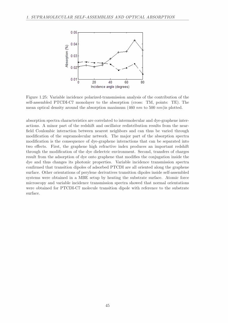
1. SUPRAMOLECULAR SELF-ASSEMBLIES AND OPTICAL ABSORPTION
Figure 1.25: Variable incidence polarized-transmission analysis of the contribution of theself-assembled PTCDI-C7 monolayer to the absorption (cross: TM, points: TE). Themean optical density around the absorption maximum (460 nm to 500 nm)is plotted.
absorption spectra characteristics are correlated to intermolecular and dye-graphene inter-actions. A minor part of the redshift and oscillator redistribution results from the near-field Coulombic interaction between nearest neighbors and can thus be varied throughmodification of the supramolecular network. The major part of the absorption spectramodification is the consequence of dye-graphene interactions that can be separated intotwo effects. First, the graphene high refractive index produces an important redshiftthrough the modification of the dye dielectric environment. Second, transfers of chargesresult from the adsorption of dye onto graphene that modifies the conjugation inside thedye and thus changes its photonic properties. Variable incidence transmission spectraconfirmed that transition dipoles of adsorbed PTCDI are all oriented along the graphenesurface. Other orientations of perylene derivatives transition dipoles inside self-assembledsystems were obtained in a MBE setup by heating the substrate surface. Atomic forcemicroscopy and variable incidence transmission spectra showed that normal orientationswere obtained for PTCDI-C7 molecule transition dipole with reference to the substratesurface.
45

1. SUPRAMOLECULAR SELF-ASSEMBLIES AND OPTICAL ABSORPTION
46

Chapter 2
Supramolecular self-assemblies
and fluorescence
Artist view of a fluorescent Janus Tecton self-assembly on graphene.Very surprisingly, a self-assembled dye monolayer on graphene, the thickness of which isof the order of a nanometer, can add a macroscopic optical absorption to the graphenesurface. Since dye molecules can emit light, would it be possible to add a fluorescent
character to graphene thanks to a self-assembled dye monolayer?
47

2. SUPRAMOLECULAR SELF-ASSEMBLIES AND FLUORESCENCE
Contents
1.1 PTCDI on graphene . . . . . . . . . . . . . . . . . . . . . . . . . . 15
1.1.1 Scanning tunneling microscopy. . . . . . . . . . . . . . . . . . . . 15
1.1.2 PTCDI-C13 Transmission spectra. . . . . . . . . . . . . . . . . . 16
1.2 Intermolecular interactions . . . . . . . . . . . . . . . . . . . . . . 19
1.2.1 Non pertubative multipolar 2D model . . . . . . . . . . . . . . . 23
1.3 Graphene-molecule interactions . . . . . . . . . . . . . . . . . . . 24
1.3.1 Electromagnetic interactions . . . . . . . . . . . . . . . . . . . . 24
1.3.2 Change of molecular conformation . . . . . . . . . . . . . . . . . 31
1.3.3 Electronic interactions . . . . . . . . . . . . . . . . . . . . . . . . 31
1.4 Dependence on the intermolecular distance . . . . . . . . . . . . 32
1.5 Dependence on the molecule-graphene distance . . . . . . . . . 37
1.6 PTCDI multilayer thin film . . . . . . . . . . . . . . . . . . . . . 41
1.7 Conclusion . . . . . . . . . . . . . . . . . . . . . . . . . . . . . . . 44
48

2. SUPRAMOLECULAR SELF-ASSEMBLIES AND FLUORESCENCE
2.1 Theoretical considerations
2.1.1 Relaxation paths
When a photon is absorbed by a dye molecule, the electron cloud distribution is changedto form the excited state of the molecule. Figure 2.1 displays the highest occupiedmolecular orbital (HOMO) and the lowest inoccupied molecular orbital (LUMO) depictingthe highest energy orbital occupied by an electron for the fundamental and the excitedstate respectively of the Me-PTCDI molecule.
Figure 2.1: LUMO (a) and HOMO (b) of Me-PTCDI. The relaxed geometry has beencalculated with the constraint DFT at the B3LYP/TZ level. Figure from ref.100
It is clear that an incident electro-magnetic field, a photon, can act on the electrondistribution through the Coulombic force to excite the dye molecule from its S0 to S1state. How a dye molecule can relax the absorbed energy? Several competing mechanismstake place in molecules, due to their unique properties and complexity.
Figure 2.2: General Jablonski Energy diagram for light-molecules interactions .
The possible desexcitations mechanisms are displayed in Figure 2.2. A molecule in itsexcited state usually relaxes rapidly to a more stable vibrational state by emitting an IRradiation. The presence of these vibrational modes is at the origin of the red-shift betweenthe absorption and fluorescence band of a dye molecule, named Stokes shift. When anexcited state is stable enough in time, the energy can be radiatively relaxed with theemission of a visible photon (fluorescence).
The energy can also be transferred to a long-lived triplet state through a so-calledintersystem crossing mechanism. From this triplet state, the energy is relaxed into theground state either by a radiative process (photoluminescence) or by a chemical process(electron transfer). The chemical process is responsible of reactive oxygen species (ROS)
49

2. SUPRAMOLECULAR SELF-ASSEMBLIES AND FLUORESCENCE
formation, which is supposed to eventually cause the dye fluorescence bleaching by modi-fication of the dye chemical structure. Finally, a last mechanism consists in total internalconversion of the energy by the emission of multiple IR radiations. For example, ADN andmelanin relax more than 99% of their absorbed energy through rapid internal conversion.This characteristic avoids the formation of ROS and thus can be considered as a protectionsince they avoid their degradation. Efficient dyes can reach very high rates of fluorescence.In free space the probability for a molecule to spontaneously emit photons is describedby the A21 Einstein coefficient. However, the fluorescence rate is strongly affected by theenvironment surrounding the molecule. It is possible to favor a radiative relaxation whenthe local electromagnetic density of modes is increased, the so-called Purcell effect.120 Butthe electromagnetic mode to which the dye molecule is coupled can be dark. For example,dye molecules on top of a metal surface can relax very rapidly their excited-state energyinto a plasmon polariton mode that involves both charge motion in the metal and elec-tromagnetic waves. However, surface plasmon polaritons do not radiate in free space (i.e.dark modes) unless certain conditions are filled.
2.1.2 Energy transfer mechanisms
Photonics active systems, such as loss compensators or lasers, require maximizing the ra-diative recombination probability (either spontaneous or stimulated). Physical phenomenathat non-radiatively absorb the excited-state energy and thus lower radiative recombina-tions are defined as quenching mechanisms, and can be categorized as either Forster orDexter mechanisms. Forster mechanism describes radiative transfer of the dye moleculeexcitation energy to any other excitation mode, mediated by the near-field, that is describ-able in the quasi-static approximation, usually donor dipole - acceptor dipole interactions.Depending on the either dark or radiative nature of this excitation acceptor mode, theForster transfer produces a quenching or an enhancement of the radiative decay, respec-tively. In the latter case, the acceptor plays the role of an optical antenna.
The above example of a dye on top of a metallic substrate enters the quenching cate-gory. The dye molecule can possibly have a higher probability of transferring excitationenergy to the plasmon polariton mode than to vacuum electromagnetic modes when iso-lated, but the plasmon mode does not radiate unless a wavevector matching mechanism,usually a prism or a grating, decouples the surface plasmon polariton to a photon.
Dexter mechanism describes excitation energy transfer through a direct exchange ofcharges by electron tunneling with another quantum system. As for the Forster mecha-nism, such energy transfer can result in an enhancement or a quenching of the radiativedecay depending on the electron acceptor radiative or dark nature respectively. However,in practice Dexter mechanism most often leads to a quenching of the molecule radiativedecay.
This mechanism happens when the dye molecule is at a tunneling distance from anothersystem. For example, if a dye is very close from a metallic surface (typically 1 nm or less),the overlap between the LUMO and the electronic wavefunction of the metal is not zero.An electron transfer probability arises, thus competing with the radiative decay path.
At typical aromatic molecules π-stacking distances (0.3 nm), Dexter energy transfer issensibly faster than Forster energy transfer.121
The understanding and the control of a dye molecule environment is therefore essentialto engineer its radiative emission.
50

2. SUPRAMOLECULAR SELF-ASSEMBLIES AND FLUORESCENCE
Figure 2.3: Artist view of graphene fluorescent non-covalent functionalization by a PTCDI-JT supramolecular self-assembly.
2.2 Janus Tecton on graphene
2.2.1 PTCDI-JT
In chapter 1, we have seen that the distinctive optical absorption signatures of self-assembled dye-graphene architectures, the structure of which were confirmed by scan-ning tunneling microscopy, can be analyzed by absorption microspectroscopy.122 How-ever, the main challenge remains the emission of light by such systems, since graphene isknown as a strong quencher through Dexter excitation transfer between the dyes and thegraphene.123,124,125 Hence, the realization of light-emitting devices based on dye-grapheneassemblies requires overwhelming Dexter transfers through introduction of an accuratelycontrolled dye-to-graphene electron barrier, from which planar flat-lying molecules are de-prived. Self-assembling building blocks of increasing three-dimensional (3D) complexityemerged recently, in particular following the so-called Janus tecton paradigm.126,127 Thesesystems have been proposed as a platform to attach functional molecular moieties at acontrolled distance from graphene.47
In this chapter, we demonstrate the first fluorescent supramolecular self-assembly ongraphene with a specifically designed 3D Janus tecton. We investigate its two-dimensionalordering by scanning tunneling microscopy (STM) and its surface optical properties byabsorption and fluorescence spectroscopies.
Results and Discussion. The 3D Janus tectons are dual-functionalized and presenttwo faces linked by a rigid spacer. One face is designed so as to steer the self-assembly ongraphene, and, for the present study, the other is a dye unit.126,127,47 More specifically,the dual-functionalized 3D tecton consists of a 3,4,9,10-perylenetetracarboxylic diimide(PTCDI) fluorophore linked to a graphene-binding pedestal by a dithiaparacyclophanepillar and a long leash made of one flexible alkyl chain and a stilbenic unit (Figure 2.4).
The pedestal also prevents the direct adsorption of the dye onto graphene and forms atunneling barrier for electrons. It is thus expected to slow down Dexter energy transfersfrom the dye to the graphene layer. The pedestal unit consists of two molecular clipslikely to steer the self-assembly of the whole entity. The clipping motif consists of twoC10H21 alkyl chains, which, upon physisorption, lay flat on the surface and aligned alongthe (110) crystallographic direction of graphene. When two such units interdigitate, theirlateral self-assembly leads to the formation of lamellae whose crystallographic structure isequivalent to the one observed upon adsorption of linear alkanes. The resulting enhanced2D crystallization energy is at the origin of the binding nature of the clip.123 In thefollowing paragraphs, this functional 3D Janus tecton will be designed as PTCDI-JT. Thespectroscopic properties of PTCDI-JT either in solution or self-assembled on graphene willbe compared to those of a PTCDI-C13 model system studied in chapter 1.The self-assembly
51

2. SUPRAMOLECULAR SELF-ASSEMBLIES AND FLUORESCENCE
Figure 2.4: Schematic Structures of the Two-Faced Janus Tecton PTCDI-JT, PTCDI-JTPedestal, and N,N′-Ditridecyl-3,4,9,10-perylenedicarboximide PTCDI-C13 Molecules.
Figure 2.5: STM images at the liquid/HOPG interface at room temperature: (a) 1:4 mix-ture of Janus tecton and pedestal molecule (60nm× 60nm, It = 8.6pA, V t = −1320mV );(b) 1:1 mixture of Janus tecton and pedestal molecule (50nm × 50nm, It = 9.9pA,V t = −1602mV ); (c) Janus tecton solution (50nm× 50nm, It = 8.6pA, V t = −1596mV ).
properties of PTCDI-JT on sp2-hybridized carbon-based substrates were investigated bySTM at the liquid/solid interface at room temperature. As already observed in chapter 1,the roughness imposed on the CVD graphene monolayer by the underlying polyethyleneterephthalate (PET) substrate makes STM observations difficult due to the poor contrastof molecules compared to this roughness. (Figure 2.6) More accurate observations areobtained with an HOPG substrate and will be preferentially used in what follows.
The image sequence displayed in Figure 2.5 corresponds to observations recorded atthe liquid/HOPG interface for three different solutions: (a) 1:4 ratio solution of PTCDI-JT to the PTCDI-JT pedestal, i.e., the naked precursor clipping unit, which constitutesthe base of the Janus tecton; (b) an equimolar mixture of the PTCDI-JT and PTCDI-JTpedestal; and (c) a solution of pure PTCDI-JT.
The independent pedestal unit is known to self-organize at the graphite surface, form-ing a two-dimensional network with the following parameters: a = 3.8nm, b = 2.1nm,α =64◦.128 Accordingly, STM images obtained with the 1:4 mixture (Figure 1a) display largedomains of a well-ordered arrangement of the clipping molecules forming the same surface
52
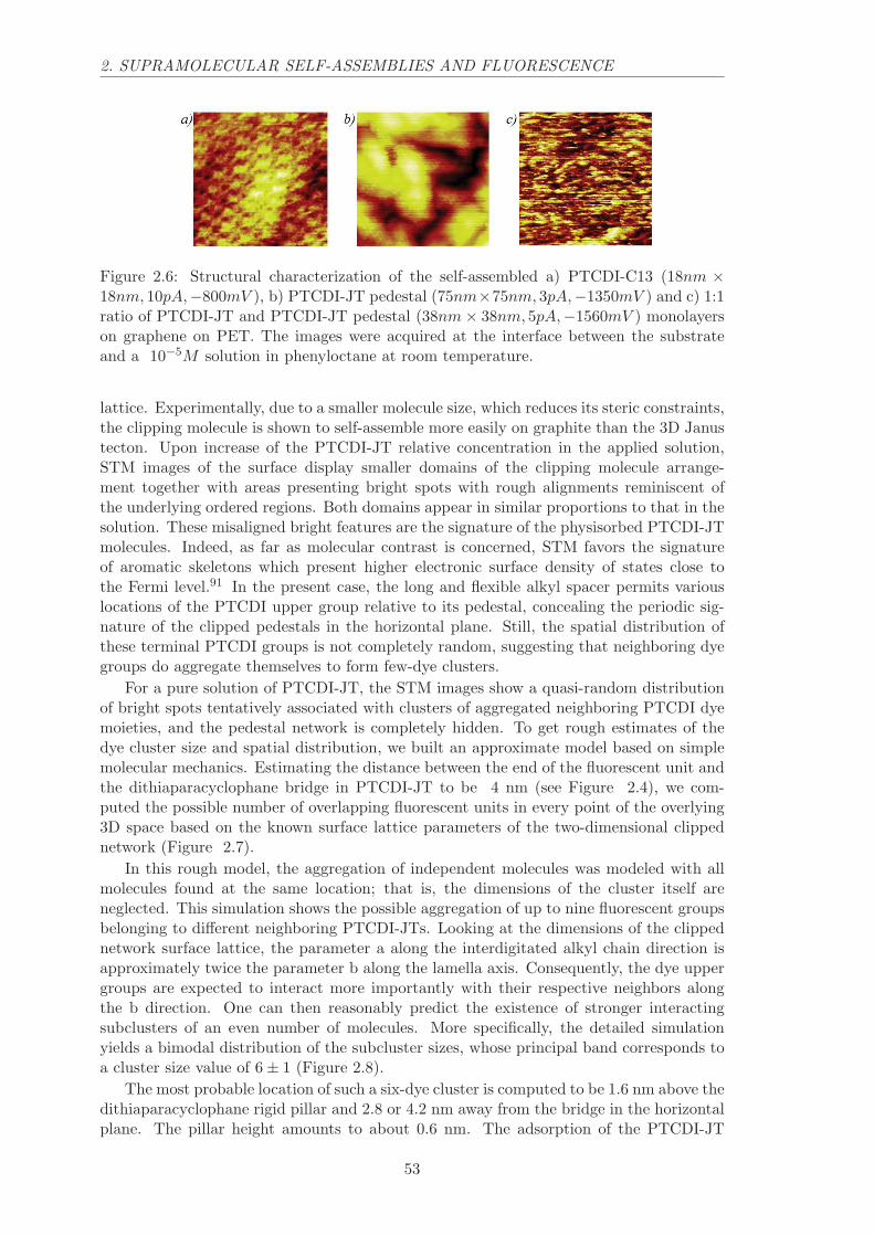
2. SUPRAMOLECULAR SELF-ASSEMBLIES AND FLUORESCENCE
Figure 2.6: Structural characterization of the self-assembled a) PTCDI-C13 (18nm ×18nm, 10pA,−800mV ), b) PTCDI-JT pedestal (75nm×75nm, 3pA,−1350mV ) and c) 1:1ratio of PTCDI-JT and PTCDI-JT pedestal (38nm× 38nm, 5pA,−1560mV ) monolayerson graphene on PET. The images were acquired at the interface between the substrateand a 10−5M solution in phenyloctane at room temperature.
lattice. Experimentally, due to a smaller molecule size, which reduces its steric constraints,the clipping molecule is shown to self-assemble more easily on graphite than the 3D Janustecton. Upon increase of the PTCDI-JT relative concentration in the applied solution,STM images of the surface display smaller domains of the clipping molecule arrange-ment together with areas presenting bright spots with rough alignments reminiscent ofthe underlying ordered regions. Both domains appear in similar proportions to that in thesolution. These misaligned bright features are the signature of the physisorbed PTCDI-JTmolecules. Indeed, as far as molecular contrast is concerned, STM favors the signatureof aromatic skeletons which present higher electronic surface density of states close tothe Fermi level.91 In the present case, the long and flexible alkyl spacer permits variouslocations of the PTCDI upper group relative to its pedestal, concealing the periodic sig-nature of the clipped pedestals in the horizontal plane. Still, the spatial distribution ofthese terminal PTCDI groups is not completely random, suggesting that neighboring dyegroups do aggregate themselves to form few-dye clusters.
For a pure solution of PTCDI-JT, the STM images show a quasi-random distributionof bright spots tentatively associated with clusters of aggregated neighboring PTCDI dyemoieties, and the pedestal network is completely hidden. To get rough estimates of thedye cluster size and spatial distribution, we built an approximate model based on simplemolecular mechanics. Estimating the distance between the end of the fluorescent unit andthe dithiaparacyclophane bridge in PTCDI-JT to be 4 nm (see Figure 2.4), we com-puted the possible number of overlapping fluorescent units in every point of the overlying3D space based on the known surface lattice parameters of the two-dimensional clippednetwork (Figure 2.7).
In this rough model, the aggregation of independent molecules was modeled with allmolecules found at the same location; that is, the dimensions of the cluster itself areneglected. This simulation shows the possible aggregation of up to nine fluorescent groupsbelonging to different neighboring PTCDI-JTs. Looking at the dimensions of the clippednetwork surface lattice, the parameter a along the interdigitated alkyl chain direction isapproximately twice the parameter b along the lamella axis. Consequently, the dye uppergroups are expected to interact more importantly with their respective neighbors alongthe b direction. One can then reasonably predict the existence of stronger interactingsubclusters of an even number of molecules. More specifically, the detailed simulationyields a bimodal distribution of the subcluster sizes, whose principal band corresponds toa cluster size value of 6± 1 (Figure 2.8).
The most probable location of such a six-dye cluster is computed to be 1.6 nm above thedithiaparacyclophane rigid pillar and 2.8 or 4.2 nm away from the bridge in the horizontalplane. The pillar height amounts to about 0.6 nm. The adsorption of the PTCDI-JT
53

2. SUPRAMOLECULAR SELF-ASSEMBLIES AND FLUORESCENCE
Figure 2.7: Map of the self-assembled PTCDI-JT tecton indicating the maximum numberof aggregated dye moieties in a parallel (left) and perpendicular (right) plane to the sub-strate, obtained as the number of intersecting half-spheres assuming each dye is locatedwithin a 4 nm distance from the center of its pedestal.
Figure 2.8: Occurrence probability of dye aggregate size.
54

2. SUPRAMOLECULAR SELF-ASSEMBLIES AND FLUORESCENCE
Figure 2.9: Spatial distribution above and away from the disulfur pillar of the 6 sized dyeaggregate.
pedestal is driven by the physisorption of its aliphatic chains. The aromatic core of thebasal unit lies flat on the graphene sheet at a respective distance of 0.33 nm.17 So, adoptinga static view of the PTCDI-JT arrangement, the clusters of dye moieties lay at about 0.33+ 0.6 + 1.6 = 2.53 nm above the graphene substrate (Figure 2.9 ).
Experimental UV-visible absorption spectra of the PTCDI-JT and the PTCDI-C13molecules in toluene are reported in Figure 2.10.
The light absorption by the clipping motif manifests itself in the UV range of thespectrum (λ < 420nm) and corresponds to the one recorded for the independent PTCDI-JT pedestal. The band at 330 nm and the shoulder at 375 nm are assigned respectivelyto the four terminal stilbene units and to the central distilbene unit. This shoulder inthe PTCDI-JT absorption spectrum appears to be 2 times larger in accordance with thepresence of another distilbene on top of the disulfur pillar. In the visible range 420nm <λ < 550nm, the PTCDI-JT absorption matches very well that of the independent PTCDI-C13 dye. This unaltered spectroscopic signature of the core dye moiety demonstratesthat the spacer effectively decouples the conjugated electron systems of fluorophore andpedestal units. The absorption spectra of self-assembled monolayers of PTCDI-JT andPTCDI-C13 on graphite are compared with a corresponding toluene solution in Figure2.11.
The relative band absorption level of the PTCDI-JT monolayer (0.4%) is nearly 6 timessmaller than that of PTCDI-C13 (2.3%). Considering a similar absorption cross section, asurface density of PTCDI-C13 of 0.5 molecules/nm2, and a 2/3 orientational factor sincethe PTCDI-C13 molecules are lying flat on the graphene surface122 whereas PTCDI-JTdye moieties are randomly oriented, one can estimate a Janus tecton surface density of0.12±0.03 molecules/nm2. This value is consistent with the surface density derived fromthe surface lattice determination by STM of a PTCDI-JT self-assembled monolayer onHOPG:127 0.14 molecules/nm2. This numerical estimate further supports the conclusionthat PTCDI-JT are regularly self-assembled on the graphene surface following the expectedbinding scheme of the clipping pedestal units taken independently.
Both PTCDI-JT and PTCDI-C13 absorption lines drastically change when self-assembledonto graphene as compared with a toluene solution (Figure 2.11). Whereas the PTCDI-C13 absorption merely consists in a rigid red-shift compared with the solution, the situa-tion is more complex for PTCDI-JT. Despite a reduced signal-to-noise ratio, an increased
55

2. SUPRAMOLECULAR SELF-ASSEMBLIES AND FLUORESCENCE
Figure 2.10: Normalized solution absorption spectra of the PTCDI-JT pedestal, PTCDI-JT, and PTCDI-C13 in toluene.
Figure 2.11: Absorption spectra of PTCDI-JT and PTCDI-C13 self-assembled ongraphene. The CVD graphene sheet has been transferred from Cu onto a transparentPET substrate prior to self-assembly. The measurements were done in transmission, ref-erenced to naked graphene. Because of the absorption of PET in the UV, the spectra arelimited to λ > 400 nm.
56

2. SUPRAMOLECULAR SELF-ASSEMBLIES AND FLUORESCENCE
Figure 2.12: Photoluminescence spectrum of self-assembled PTCDI-JT on graphene (blue)compared with PTCDI-C13 reference signals in toluene (green, rescaled), self-assembledon graphene (black), and in the microcrystal solid state (red, rescaled). The moleculesare excited by a continuous wave laser operating at 532 nm wavelength, which hides theprincipal fluorescence band (0-0 line) for all the systems.
weight of higher-order vibronic replicas is perceptible and the rising edge appears lessabrupt, which can correspond to a spectral broadening. The red-shift observed for PTCDI-C13 is explained by the adsorption of its aromatic core, which lies flat on graphene at atypical π-stacking distance of 0.33 nm.122 As inferred from STM analysis in the previoussection, for PTCDI-JT, the corresponding distance is much larger. According to the staticmodel discussed above, the distance from the dye moieties to the graphene is typically 7times larger (2.5 nm), which prevents such interactions. In contrast with PTCDI-C13,the dye moieties of PTCDI-JT form few-molecule clusters. The increase of higher-ordervibronic bands is typical of a H-aggregate behavior which can result from a π-stackingconfiguration inside clusters.129,130,59 The spectral broadening of the vibronic spectralfeatures, already present in self-assembled PTCDI-C13, is further increased for PTCDI-JT. This probably reflects the inhomogeneity of the dye-moiety assembly, as evidenced bySTM imaging of the PTCDI-JT tectons, which evidence dye clusters with various sizes.
The main result of this chapter is presented in Figure 2.12, in which the fluorescencesignals of the PTCDI-JT molecule self-assembled on graphene are compared with thoseof the PTDCI-C13 reference as recorded in solution, in a self-assembled monolayer ongraphene, or in solid-state microcrystals as formed by casting the same PTCDI-C13 toluenesolution onto naked fused silica instead of graphene.
A photoluminescence signal of the PTCDI-JT self-assembly on graphene is readilymeasurable, whereas no such signal can be detected from the PTCDI-C13 ordered domainson the same substrate. Hence, the design of PTCDI-JT based on a spacer between thedye and graphene actually reduces the energy transfer rate. The measured fluorescencequantum yield is still low, estimated in the range of 2 × 10⁻⁵ to 2 × 10⁻⁶ by integrating
57

2. SUPRAMOLECULAR SELF-ASSEMBLIES AND FLUORESCENCE
the fluorescence signal between 560 and 745 nm for an excitation at 532 nm. Since theradiative decay rate of PTCDI is on the order of 10−9s−1, the quenching rate is in the range1014s−1 to 1015s−1. Although still high, this value is compatible with a residual Forsterresonance energy transfer, the Dexter transfer being slower for the distances betweendye and graphene that were estimated above. The formation of clusters also stronglyaffects the characteristics of luminescence. Although the above-mentioned H-aggregatecoupling is supposed to slow the radiative decay in favor of the quenching, PTCDI-C13is fluorescent in the solid state, as shown with the fluorescence of microcrystals formedon silica. Nonradiative relaxations are thus hindered by the strong interactions betweenstacked molecules. The fluorescence spectrum of PTCDI-JT self-assembled onto graphene(Figure 2.12, blue curve) is intermediate between that of the PTCDI-C13 solvated intoluene (green curve) and that of PTCDI-C13 microcrystals on silica (red curve), showinga progressive displacement of the oscillator strength toward higher vibrational replicaswith cluster size, consistent with the H-aggregate-like coupling deduced from absorptionspectroscopy. A shorter exciton coherence length in self-assembled clusters is consistentwith the involvement of a small number of dye groups, spatially limiting the coherentdelocalization of the exciton, which is on the order of 2 nm for similar crystals.130,131
Furthermore, the H-aggregation geometry could be perturbed from a perfect π-stackingby the spacer steric hindrance. Instead of being parallel, aromatic cores can adopt an anglethat partially decouples the transition dipole moments. This suggests that the controlledformation of few-molecule dye clusters plays a role in the restoration of luminescence. Notethat the Janus tecton surface fluorescence band is slightly redshifted from the PCTDI-C13ones, consistent with its redshifted absorption.
2.2.2 TBC8-JT
PTCDI-JT forms small aggregates once self-assembled on the graphene surface due to along and flexible alkyl chain linking the disulfur bridge and the perylene dye group. A morerigid Janus tecton is desired to gain control on the optical properties of such graphenenon-covalent functionalization, for example avoiding the formation of small aggregates.The Janus tecton approach is further explored with TBC8-JT (see chapter 1) which doesnot possess such flexible group in its structure. The optically active group is directly linkedto the disulfur bridge. Scanning tunneling images confirm a periodic network formationwithout any aggregation. Figure 2.13 displays the absorption and photoluminescencespectra of TBC8-JT either dissolved in phenyloctane or self-assembled on graphene.
A fluorescence signal is detected from the self-assembled TBC8-JT monolayer ongraphene (green curve). Surprisingly, the photoluminescence spectrum band and globalshape of self-assembled TBC8-JT monolayer on graphene is quite similar to the samemolecule in a phenyloctane solution. Since the absorption band is redshifted once ad-sorbed on the graphene surface, one should have expected to see this effect also on thephotoluminescence spectrum that is a preservation of the Stokes shift. The 420 meV Stokesshift of TBC8-JT in a phenyloctane solution is reduced to 230 meV once self-assembledon the graphene surface.
The measured fluorescence lifetime of TBC8-JT in solution when exciting at 400 nmby a doubled femtosecond Ti:Sapphire laser is 4.0 ns. When self-assembled on graphene,the fluorescence lifetime is reduced to 2.7 ns. Hence, even if no differences can be observedon fluorescence spectra, fluorescence lifetime measurements reveal the decrease of theradiative desexcitation lifetime and thus the increase of the non-radiative decay. A Forsterquenching by the graphene layer may be the cause of this fluorescence lifetime perturbationsince the optical active group seems too far away from the graphene surface for chargetransfer to occur. However, it is still not clear why the fluorescence spectrum is not shiftedidentically to the absorption spectrum and we prefer to do not draw a conclusion due to the
58

2. SUPRAMOLECULAR SELF-ASSEMBLIES AND FLUORESCENCE
Figure 2.13: Normalized photoluminescence and absorption spectra of self-assembledTBC8-JT on graphene (photoluminescence: light green, absorption: light blue) comparedwith TBC8-JT reference signals in phenyloctance (photoluminescence: dark green, ab-sorption: dark blue). The molecules are excited by a doubled femtosecond Ti:Sapphirelaser operating at 400 nm wavelength.
resemblance between the solution and self-assembled spectra and to the long fluorescencelifetime. Small molecular aggregates decoupled from graphene have possibly remained onthe surface, taking little part in the absorption spectrum due to their limited numberbut having a significant weight in the fluorescence spectrum due to their decoupling fromgraphene.
2.3 Multilayers of Perylene derivatives
Few dyes molecules display fluorescence in solid state. Their aggregation often dramati-cally changes their photophysics properties by shifting absorption band and increasing ra-diative decay rate. Non radiative path are usually favored due to interactions of moleculeswith the close environment, such as charge transfers resulting in Dexter quenching. How-ever, fluorescent dyes in the solid state are highly desirable since this state represents thehighest reachable density for these emitters. Such compact emitter systems could lead tothe miniaturization of gain media for laser systems and become perfect media for inter-acting with highly confined electromagnetic modes paving the way to the realization ofnanolasers.
In the following, we study the optical response of perylene derivatives in a solid state.Figure 2.14 displays the molecular structures and the fluorescence spectra of a 30 nm thickPTCDI-C7 thin film, a 1 nm thick PTCDI-C7B thin film and a PTCDI-tBuPh crystalproduce by the evaporation of a PTCDI-tBuPh in toluene solution on a glass coverslip atambient conditions.
59

2. SUPRAMOLECULAR SELF-ASSEMBLIES AND FLUORESCENCE
Figure 2.14: a). Molecular structures of PTCDI-C7, PTCDI-tBuPh and PTCDI-C7B.b). Normalized fluorescence spectra from a 30 nm thick PTCDI-C7 thin film (blue), a 1monolayer PTCDI-C7B thin film (green) and a PTCDI-tBuPh cristal evaporated underambient condition on a SiO2 coverslip (red). The systems are excited with a 532 nmcontinuous wave laser.
From the different perylene derivative spectra three main bands can be isolated at630 nm, 680 nm and 730 nm that correspond to transitions from an excitonic state tothe vibrational replicas of the molecule fundamental state.132 The energy gap betweenthese three bands are respectively 145 meV (1170 cm−1) and 125 meV (1010 cm−1).These values are a slightly smaller than C-C vibrational modes in conjugated aromaticmolecules that fall around 174 meV (1400 cm−1).
The fluorescence spectra peak at 680 nm for the PTCDI-C7 and PTCDI-tBuPh systemsand at 730 nm for the PTCDI-C7B system, revealing a large Stokes shifts since the opticalabsorption peaks at 500 nm for the PTCDI-C7 and PTCDI-tBuPh systems and at 560 nmfor the PTCDI-C7B system (Chapter 1). The formation of self-trapped excitons due tostrong exciton-phonon coupling results in low energy states (ST), lower than free excitonstates, that can explain such large Stokes shifts in these solid state systems.133
A direct comparison with a R6G/PMMA reference system gives a fluorescent quantumyield of approximately 10% for the 30 nm thick PTCDI-C7 thin film.
Each systems display various oscillator strength distributions over these bands. ThePTCDI-C7 film decays mainly radiatively with the ST-1 path corresponding to a transitionbetween the ST state and the first vibronic replica of the electronic fundamental state (680nm band), as PTCDI-tBuPh does. However, the 630 nm band is not visible for the latter.Finally, the ST-2 transition (730 nm band) is the preferential radiative decay path forthe PTCDI-C7B. These various oscillator strength distribution over vibronic replicas mayresult from H/J aggregate behavior arising from differences in the π-stacking geometry ofthe perylene aromatic cores.59
2.4 Conclusion
In summary, we have achieved the first fluorescent molecular self-assembly on graphene.This milestone has been made possible thanks to the development of a 3D Janus tectonembedding a PTCDI dye away from the substrate plane together with the use of CVDgraphene as an optics-compatible 2D substrate. A fluorescent noncovalent functionaliza-tion of graphene could help to alter the photonic properties of this zero-gap semiconductingmonolayer or to alter photonic properties of any third-party surfaces through transfer ofmonolayer CVD graphene. Furthermore, we obtained a dense three dimensional dye self-assembly displaying relatively good quantum fluorescence efficiency. This dense packing offluorescent molecules could be of prime importance for maximizing the coupling between
60

2. SUPRAMOLECULAR SELF-ASSEMBLIES AND FLUORESCENCE
emitters and strongly confined electromagnetic modes such as plasmonic waves.
61

2. SUPRAMOLECULAR SELF-ASSEMBLIES AND FLUORESCENCE
62

Chapter 3
Vibrations of supramolecular
self-assemblies on graphene
Artist view of the Mambo mode, a vibrational mode coupled between graphene and aself-assembled molecule on its surface.
The study of this mode characteristics may lead to the development of a sensoridentifying aromatic molecules adsorbed on the graphene surface.
63

3. VIBRATIONS OF SUPRAMOLECULAR SELF-ASSEMBLIES ON GRAPHENE
Contents
2.1 Theoretical considerations . . . . . . . . . . . . . . . . . . . . . . 49
2.1.1 Relaxation paths . . . . . . . . . . . . . . . . . . . . . . . . . . . 49
2.1.2 Energy transfer mechanisms . . . . . . . . . . . . . . . . . . . . . 50
2.2 Janus Tecton on graphene . . . . . . . . . . . . . . . . . . . . . . 51
2.2.1 PTCDI-JT . . . . . . . . . . . . . . . . . . . . . . . . . . . . . . 51
2.2.2 TBC8-JT . . . . . . . . . . . . . . . . . . . . . . . . . . . . . . . 58
2.3 Multilayers of Perylene derivatives . . . . . . . . . . . . . . . . . 59
2.4 Conclusion . . . . . . . . . . . . . . . . . . . . . . . . . . . . . . . 60
64
3. VIBRATIONS OF SUPRAMOLECULAR SELF-ASSEMBLIES ON GRAPHENE
As explained in previous chapters, supramolecular self-assemblies on graphene provideopportunities for the design and the manufacturing of innovative hybrid photonic devices.
On its part, Raman spectroscopy has become an invaluable tool to characterize graphenewith or without any functionalization since the active vibrations convey important infor-mation about graphene purity, defects or doping.134 In the framework of chemical doping,most of the information about electron transfer is given by the width and the positionof the G and 2D bands of graphene.135 To our knowledge, other couplings, in particularmechanical coupling between graphene and adsorbed organic molecules, have not yet beenexplored.
The complete fluorescence quenching of resonant dyes adsorbed on graphene, by Dexterprocesses, allows a clear observation of Raman scattering. Actually, even under resonantconditions, Raman signals are orders of magnitude weaker than fluorescence. Moreover,it has been recently discovered that graphene can enhance the Raman signal of adsorbedmolecules by a process which is physically similar to the chemical contribution to surface-enhanced Raman scattering (SERS).136 These two effects represent a unique opportu-nity to explore the physical vibrational properties of systems comprising self-assembledmolecules adsorbed on graphene by resonance Raman spectroscopy.137 Recent theoreti-cal work on the interpretation of Raman spectra modified by neighbor interactions willopportunely supplement such studies.138,139
In this chapter, we study the vibrational coupling between a free-standing graphenemembrane and organic molecules self-assembled on its surface: a DFT simulation illus-trates in a simple system the nature of coupled graphene-adsorbate vibrational modes.Experimental Raman spectra of a self-assembled resonant dye on graphene confirm theexistence of such coupled modes. Scanning tunneling microscopy is performed to studythe effect of the molecular network on the graphene-molecule vibrational coupling.
3.1 Introduction to Raman scattering
The vibrational modes of a system manifest themselves in the interaction with light. Thesignature of such low frequency modes (usually in the 0 − 90 THz or 0 − 3000 cm−1 or0 − 370 meV or 3.3 − ∞ µm range) can be probed by several ways. In the case of adye absorbing in the visible range, these vibrational properties can be seen in the visibleabsorption spectrum, in the infrared absorption spectrum and in the Raman scattering oflight.
The origin of Raman scattering can be understood by approximating the system po-larizability α in a Taylor series approach.
When atom vibrations are involved in the polarizability resonance, one can introducethe displacement parameter dq which describes the motion of atoms in time about theirequilibrium position.
dq = q0cos(ωvt) (3.1)
where ωv represent the angular frequency of a vibrational mode. Since the atom displace-ment remains quite small, the polarizability can be evaluated around the atom equilibriumposition with a Taylor series:
α = α0 +dα
dq(0)dq +
1
2
d2α
dq2(0)dq2 (3.2)
The dipole moment µ of the system can then be expressed with an incident electric fieldE = E0cos(ωt) :
65

3. VIBRATIONS OF SUPRAMOLECULAR SELF-ASSEMBLIES ON GRAPHENE
Figure 3.1: Anti-symmetric (a) and symmetric (b) vibrational mode of the CO2 molecule.(a) is not Raman active whereas (b) is.
µ = αE = α0E0cos(ωt) +dα
dq(0)q0E0cos(ωt)cos(ωvt) +
1
2
d2α
dq2(0)E0q0cos(ωt)cos
2(ωvt)
(3.3)
µ =
[
α0 +1
4
d2α
dq2(0)q20
]
E +1
2
dα
dq(0)q0E0
[
cos((ω + ωv)t) + cos((ω − ωv)t)
]
(3.4)
+1
8
d2α
dq2(0)E0q
20
[
cos((ω + ωv)t) + cos((ω − 2ωv)t)
]
The above equation shows that induced dipole moments are created at the frequencyω which correspond to elastic scattering but also at inelastic frequencies ω−ωv and ω+ωv
which are respectively referred to Stokes and anti-Stokes Raman scattering. From theabove equation, these processes exist if the derivative of the polarizability with referenceto the displacement is non null at the equilibrium position. As an example, figure 3.1represents two vibrational modes of the CO2 molecule. The polarizability in the anti-symmetric mode has a symmetrical behavior with reference to atom displacement aboutthe equilibrium position. Therefore, dα
dqevaluated at the equilibrium position is zero and
the mode is not Raman active, meaning no Raman processes can exist. This is not the casefor the symmetric vibrational mode since the polarizability does not behave identically forpositive or negative atom displacement about their equilibrium position. dα
dq(0) is non zero
meaning that this mode is Raman active. The above equation also shows that overtones inRaman spectra are related to higher-order derivatives of the polarizability with referenceto displacement. For example, first harmonic exist if d2α
dq2(0) is non zero.
We compare in a Jablonski diagram (figure 3.2) the different processes where vibra-tional modes are involved for a dye absorbing light in the visible.
The presence of vibrational states can be probed by the absorption of IR photons withenergy corresponding to the energy gap between two vibrational modes, corresponding toprocess (a) in figure 3.2. Vibrational modes are observable if a small atom displacement
induces a variation of dipolar moment, i.e. d2µdq2
(0) is non zero. Raman scattering can occurat any incident photon energy. When this photon energy is not able to excite any state ofthe molecule, the process involves a virtual state and is referred as non-resonant Ramandiffusion (process (b) in figure 3.2). In the reverse situation, that is when the photonenergy is able to excite a molecular level, one refers to resonant Raman scattering. Inthe case of a fluorescent dye, the fluorescence signal can then hide the Raman scatteringsignal since it displays exactly the same energy.
Finally, the presence of vibrational states can be probed in both the absorption andfluorescence spectrum since photon absorption (respectively photon spontaneous emission)is possible from the lowest energy vibrational state of the electronic fundamental (respec-tively excited) state to the various vibrational states of the electronic excited (respectivelyfundamental) state.
66

3. VIBRATIONS OF SUPRAMOLECULAR SELF-ASSEMBLIES ON GRAPHENE
Figure 3.2: (a). Infrared absorption between the vibrational states 0-1 and 0-2 of theelectronic fundamental state. (b). Non resonant Raman scattering implying a virtualstate. (c) Visible absorption between the 0 electronic fundamental state and the 0*, 1*and 2* vibrational replicas of the electronic excited state.
The major difference between IR absorption and Raman scattering on one side andvisible absorption on the other side is the fact that the energy of vibrational states is notprobed with the same accuracy. Since visible absorption involves two different electronicstates, spectral diffusion comes into the play and broadens consequently the transitions atambient conditions. Thermal fluctuations (kT = 25 meV corresponding to a wavenum-ber of 200 cm−1) and other dephasing processes significantly broadens the absorptionlineshape. Raman scattering and IR absorption do not have these limitations and widthsas small as 20 cm−1 = 2.5 eV can be observed under ambient conditions.
3.2 Graphene Raman spectrum
Raman spectroscopy is a powerful tool for the characterization of graphene. It can giveinsight about its purity in terms of defect density, number of stacked sheet, dopants.135
A detailed understanding of graphene vibrational processes is needed before studyingvibrational coupling with self-assembled monolayers on its surface.
Figure 3.3 displays the honeycomb lattice formed by the carbon atoms of graphene.The primitive cell of this Bravais lattice can be defined by the two primitive vectors in thedirect space a1 and a2. In the reciprocal space, primitive vectors b1 and b2 are deducedfrom the two direct space primitive vectors as indicated in figure 3.3 where R representsa 90◦ rotation matrix.
The center of the Brillouin zone is called Γ point, vertices are referenced as K points,and the edge middles as M points.
Example Raman spectra of pristine graphene and damaged graphene are presentedin figure 3.4. As displayed in spectra, three bands named D, G and 2D at 1350 cm−1,1580 cm−1 and 2700 cm−1 respectively are predominant. These bands correspond to twomain vibrational modes on which we will focus in the following.
Scheme 3.5 represents the graphene lattice deformation due to the carbon atom motionof the vibrational mode implicated in the G band.
67

3. VIBRATIONS OF SUPRAMOLECULAR SELF-ASSEMBLIES ON GRAPHENE
Figure 3.3: Graphene lattice in real and reciprocal space.
Figure 3.4: Example spectra : graphene flake. (a) A pristine flake showing only the G, 2Dand 2D’ bands. (b) A damaged flake, which shows the D and D’ bands, as well as theircombination D+D’. Reproduced from ref.135
Figure 3.5: Graphene lattice (black) and its deformation (dash dark blue) for normalvibrational modes (a) and (b) corresponding to the G band in graphene Raman spectrum.
68
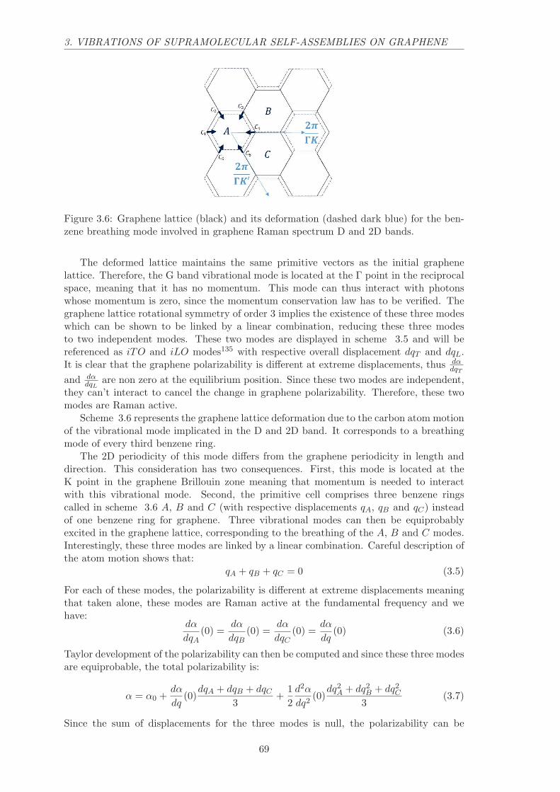
3. VIBRATIONS OF SUPRAMOLECULAR SELF-ASSEMBLIES ON GRAPHENE
Figure 3.6: Graphene lattice (black) and its deformation (dashed dark blue) for the ben-zene breathing mode involved in graphene Raman spectrum D and 2D bands.
The deformed lattice maintains the same primitive vectors as the initial graphenelattice. Therefore, the G band vibrational mode is located at the Γ point in the reciprocalspace, meaning that it has no momentum. This mode can thus interact with photonswhose momentum is zero, since the momentum conservation law has to be verified. Thegraphene lattice rotational symmetry of order 3 implies the existence of these three modeswhich can be shown to be linked by a linear combination, reducing these three modesto two independent modes. These two modes are displayed in scheme 3.5 and will bereferenced as iTO and iLO modes135 with respective overall displacement dqT and dqL.It is clear that the graphene polarizability is different at extreme displacements, thus dα
dqT
and dαdqL
are non zero at the equilibrium position. Since these two modes are independent,they can’t interact to cancel the change in graphene polarizability. Therefore, these twomodes are Raman active.
Scheme 3.6 represents the graphene lattice deformation due to the carbon atom motionof the vibrational mode implicated in the D and 2D band. It corresponds to a breathingmode of every third benzene ring.
The 2D periodicity of this mode differs from the graphene periodicity in length anddirection. This consideration has two consequences. First, this mode is located at theK point in the graphene Brillouin zone meaning that momentum is needed to interactwith this vibrational mode. Second, the primitive cell comprises three benzene ringscalled in scheme 3.6 A, B and C (with respective displacements qA, qB and qC) insteadof one benzene ring for graphene. Three vibrational modes can then be equiprobablyexcited in the graphene lattice, corresponding to the breathing of the A, B and C modes.Interestingly, these three modes are linked by a linear combination. Careful description ofthe atom motion shows that:
qA + qB + qC = 0 (3.5)
For each of these modes, the polarizability is different at extreme displacements meaningthat taken alone, these modes are Raman active at the fundamental frequency and wehave:
dα
dqA(0) =
dα
dqB(0) =
dα
dqC(0) =
dα
dq(0) (3.6)
Taylor development of the polarizability can then be computed and since these three modesare equiprobable, the total polarizability is:
α = α0 +dα
dq(0)
dqA + dqB + dqC3
+1
2
d2α
dq2(0)
dq2A + dq2B + dq2C3
(3.7)
Since the sum of displacements for the three modes is null, the polarizability can be
69
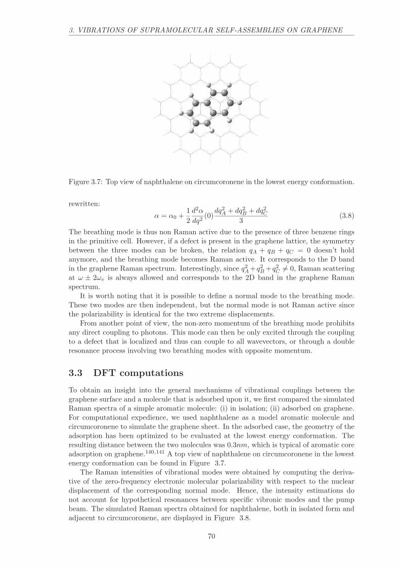
3. VIBRATIONS OF SUPRAMOLECULAR SELF-ASSEMBLIES ON GRAPHENE
Figure 3.7: Top view of naphthalene on circumcoronene in the lowest energy conformation.
rewritten:
α = α0 +1
2
d2α
dq2(0)
dq2A + dq2B + dq2C3
(3.8)
The breathing mode is thus non Raman active due to the presence of three benzene ringsin the primitive cell. However, if a defect is present in the graphene lattice, the symmetrybetween the three modes can be broken, the relation qA + qB + qC = 0 doesn’t holdanymore, and the breathing mode becomes Raman active. It corresponds to the D bandin the graphene Raman spectrum. Interestingly, since q2A+q2B+q2C 6= 0, Raman scatteringat ω ± 2ωv is always allowed and corresponds to the 2D band in the graphene Ramanspectrum.
It is worth noting that it is possible to define a normal mode to the breathing mode.These two modes are then independent, but the normal mode is not Raman active sincethe polarizability is identical for the two extreme displacements.
From another point of view, the non-zero momentum of the breathing mode prohibitsany direct coupling to photons. This mode can then be only excited through the couplingto a defect that is localized and thus can couple to all wavevectors, or through a doubleresonance process involving two breathing modes with opposite momentum.
3.3 DFT computations
To obtain an insight into the general mechanisms of vibrational couplings between thegraphene surface and a molecule that is adsorbed upon it, we first compared the simulatedRaman spectra of a simple aromatic molecule: (i) in isolation; (ii) adsorbed on graphene.For computational expedience, we used naphthalene as a model aromatic molecule andcircumcoronene to simulate the graphene sheet. In the adsorbed case, the geometry of theadsorption has been optimized to be evaluated at the lowest energy conformation. Theresulting distance between the two molecules was 0.3nm, which is typical of aromatic coreadsorption on graphene.140,141 A top view of naphthalene on circumcoronene in the lowestenergy conformation can be found in Figure 3.7.
The Raman intensities of vibrational modes were obtained by computing the deriva-tive of the zero-frequency electronic molecular polarizability with respect to the nucleardisplacement of the corresponding normal mode. Hence, the intensity estimations donot account for hypothetical resonances between specific vibronic modes and the pumpbeam. The simulated Raman spectra obtained for naphthalene, both in isolated form andadjacent to circumcoronene, are displayed in Figure 3.8.
70

3. VIBRATIONS OF SUPRAMOLECULAR SELF-ASSEMBLIES ON GRAPHENE
Figure 3.8: From bottom to top: Simulated Raman spectrum for circumcoronene (orange),naphthalene (light green), and naphthalene adjacent to circumcoronene (dark green) whereonly the naphthalene Raman signal is considered even if the circumcoronene is present.
The results obtained for the isolated molecule are consistent with other computationsand experimental measurements,142 as concerns both the vibrational frequencies and theirassignments. The coupling between naphthalene and circumcoronene manifests itself intwo effects.
First, a subset of the Raman-active resonances are shifted by 10−20cm−1 toward higherfrequencies. A detailed comparison of vibration assignments and adsorption-induced high-frequency shifts of the corresponding bands shows that the affected vibrations are system-atically those involving out-of-plane nuclear motions, in particular the out-of-plane C-C-Cbending (508cm−1) and the modes combining in-plane aromatic C-C stretching with out-of-plane C-H bending (1166cm−1, 1240cm−1, 1459cm−1). In contrast, the in-plane normalmodes involving only aromatic C-C stretching are not affected by the adsorption (759cm−1
breathing-like mode, 1017cm−1, 1375cm−1, 1572cm−1 and 1626cm−1 ring-deformationmodes). Notice that the in-plane CH-stretching group around 3050cm−1 is also not af-fected by the adsorption. The increase of the frequencies with adsorption shows thatthe distance of the adsorbate corresponds to a repulsive contact. The absence of shiftinduced by adsorption for in-plane vibrations shows that this contact doesn’t affect thein-plane potential, and π − π interactions have no significant influence on aromatic C-Cbond strengths.
Secondly, a new vibration, absent from both isolated naphthalene or circumcoronene,appears at low frequency (80cm−1) in the Raman spectrum of naphthalene when adsorbedonto circumcoronene. The visualization of nuclear motion in this combined molecularstructure shows that this vibrational mode is delocalized on naphthalene and circum-coronene, and may be described as a swinging motion of the whole naphthalene moleculearound its longer axis. For this reason, it will hereafter be referred as ”molecular mambo”mode. Similarly with the first observation, this mode involves exclusively vertical nuclearmotions, i.e. motions perpendicular to the graphene plane. The non-covalent nature of thecorresponding vertical bonds explains the low frequency of the mambo mode comparede.g. to the stretching of covalent C-C bonds. Notice also that this mode is Raman-activethanks to a lateral shift of the naphthalene equilibrium position compared to circum-coronene, which breaks the symmetry between both sides of the tilt deformation. Theabsence of such a shift in the other in-plane direction justifies that no short-axis mambomode is predicted.
Although based on a simplistic model, these illustrative observations will provide guide-
71

3. VIBRATIONS OF SUPRAMOLECULAR SELF-ASSEMBLIES ON GRAPHENE
Figure 3.9: DFT computed Raman spectra for PTCDI-C13 (blue) and PTCDI-2C6a (red)in vacuum.
lines for analyzing the Raman spectra of more complex self-assembled dye monolayers ongraphene.
3.4 Resonant self-assembled monolayer on graphene
In chapter 1, we have seen that PTCDI-C13 and PTCDI-2C6a form self-assembled mono-layer at the graphene surface with two distinct geometries. Furthermore, transmissionabsorption spectra showed that both systems absorb light at a wavelength of 532 nm, andmay thus be good candidates for resonant Raman scattering experiments.
Figure 3.9 displays the computed Raman spectra of isolated PTCDI-C13 and PTCDI-2C6a. The two spectra are highly similar. The computation only predicts a difference inthe frequency of the ∼ 1050 cm−1 vibrational mode: from 1050 cm−1 for PTCDI-C13 to1040 cm−1 for PTCDI-2C6a. The visualization of the 1050 cm−1 vibrational mode showsthat this vibration involves aromatic C-C stretching with a symmetric elongation of thealiphatic C-N bonds at both extremities of the PTCDI aromatic core. The substitutionof the highly inertial alkyl chain by a light hydrogen atom explains the predicted low-frequency shift for this normal mode. As most of the vibrational normal modes are alreadyRaman-active in the symmetric PTCDI-C13 molecule, no new active Raman modes areproduced by the breaking of this symmetry. PTCDI-C13 has twice as many C-H bonds asPTCDI-2C6a. Consequently, the associated 2900 cm−1 Raman vibration group is twiceas intense as in the PTCDI-C13 case.
For both molecules, the overlap between graphene sp2 orbitals and the aromatic corein the self-assembled structures results in an ultrafast quenching of the electronic excita-tions.143 Hence, these systems are not fluorescent as shown for PTCDI-C13 in chapter2.111 We can therefore observe Raman signals by using resonant excitation of the moleculardye, without disturbance from any fluorescence. The resonance enhancement is necessaryto detect a signal from only one monolayer of molecules and to filter out other contri-butions from non-resonant systems such as the substrate. Moreover, the surface densityin self-assembled PTCDI derivatives on graphene is very high: 0.45 molecules.nm−2.(cf.chapter 1) Since Raman intensity is proportional to the number of probed molecules, thisapproach enables the experimental observation of molecular vibrations with an unprece-dented signal to noise ratio. Finally, the Raman enhancement by graphene also facilitates
72

3. VIBRATIONS OF SUPRAMOLECULAR SELF-ASSEMBLIES ON GRAPHENE
Figure 3.10: From bottom to top: Experimental Raman spectra for suspended graphene(black), DFT computed Raman spectrum for PTCDI-C13 (light blue, rescaled for easiercomparison) in vacuum, and self-assembled PTCDI-C13 on suspended graphene (blue).Inset: self-assembled PTCDI-C13 on suspended graphene x10.
observation of self-assembled PTCDI-C13 and PTCDI-2C6a Raman signals.136
Figure 3.10 displays the experimental Raman spectrum of graphene, PTCDIC13 aswell as DFT computed PTCDI-C13.
First, we compare in figure 3.10 the Raman experimental spectra of self-assembledPTCDI-C13 with that of the neat graphene and with the simulated Raman spectrum ofisolated PTCDI-C13. As concerns neat suspended graphene film, the G band peak has awidth of 19 cm−1 (full width half maximum); the 2D band corresponding to the mechanisminvolving two iTO phonons is located at 2685 cm−1 and its Raman intensity ratio to theG band intensity is 2.2. We detect a D band at 1345 cm−1 with very low Raman intensity,indicating a small density of defects. Such characteristics are usually considered reliableindicators of high quality graphene. The D+D′′ band is also present at 2465 cm−1 as wellas the 2D′ band at 3257 cm−1. We see also a three-phonon process at 4275 cm−1 whichwe assign to G+2D.
The Raman spectrum of self-assembled PTDCI-C13 on graphene, displayed in figure3.10, is in accordance with the DFT computed spectrum in the spectral range below1700 cm−1, within the limit of fundamental frequencies (since, as mentioned earlier, ourcomputations do not predict overtones and combinations). Two differences appear in thispart of the experimental Raman spectrum in comparison with the result of DFT modeling.First, a rigid shift of the spectrum toward higher frequencies can be observed. Secondly,and most interestingly, a broad low frequency band appears at 230 cm−1. This observationechoes the low frequency coupled molecule-graphene mambo modes evoked before. Thus,by analogy, we assign this band to such mambo modes corresponding to oscillations aroundthe N-N axis of PTCDI-C13.
In the spectral range above 1700 cm−1, the experimental Raman spectrum of self-assembled PTDCI-C13 on graphene presents bands to be attributed to replicas of lower en-ergy fundamental modes involving single vibrational quanta. As expected, these overtonesand combinations of frequencies appear at multiple and sum frequencies of fundamentalmodes. Accordingly, their intensities can be reproduced by a simple autocorrelation S ∗Sof the spectrum S comprised in the [0 − 1700 cm−1] region – a technique that providesfor vibrational combinations to be excited in a single Raman event with a sum-frequency
73

3. VIBRATIONS OF SUPRAMOLECULAR SELF-ASSEMBLIES ON GRAPHENE
Figure 3.11: From top to bottom: Fundamental vibrational Raman spectrum (blue) forPTCDI-C13, Reconstructed spectrum (light blue), and full experimental spectrum (darkblue).
Stokes shift.
As shown in Figure 3.11, this operation faithfully replicates the spectrum above1700 cm−1 by introducing one single overall scale parameter k such that the total re-constructed spectrum is written:
St = S + kS ∗ S
The weighting factor k characterizes the strength of the process associating two vibra-tional quanta with respect to fundamental transition processes; from a classical point ofview this reflects anharmonicity in the potential corresponding to each oscillator. Thisproperty illustrates the common nature of the vibrations that are the most Raman activeunder resonance conditions at a wavelength of 532 nm, which correspond to combinationsof aromatic C-C stretching. Consistently, the common ratio of second-order to first-orderRaman bands is the same as the ratio of the second (0-2) to the first (0-1) vibronic replicain the absorption spectrum. Notably, the Raman response of neat graphene doesn’t followthe same rule. This difference is due to selection rules arising from the 2D-translationalinvariance of graphene.
By subtracting the full experimental spectrum from the convoluted spectrum, no2900 cm−1 response that could be attributed to C-H stretching group emerges from thenoise. This low efficiency is attributed to a resonance effect: only the conjugated aromaticpart of the molecule is excited, and aliphatic CH vibrations are not electronically coupledto it. Graphene Raman bands, in particular the large 2D one, are also not discernible,indicating a surprisingly low response of graphene compared to PTCDI-C13.
We compare in Figure 3.12 the experimental Raman spectrum of self-assembledPTCDI-C13 and PTCDI-2C6a on suspended graphene. Once again, DFT computed spec-tra of isolated molecules displayed in figure 3 match very well their experimental data whenadsorbed onto graphene. This shows the weakness of interactions between graphene andthe conjugated kernels of adsorbed molecules as concerns in-plane aromatic C-C stretchingvibrations, consistent with our conclusions on the illustrative simulation of naphthalene oncircumcoronene. In particular, the predicted 10 cm−1 low-frequency shift of the 1050 cm−1
mode from PTCDI-C13 to PTCDI-2C6 is clearly observable experimentally, whereas theother bands keep the same frequencies. This illustrates the accuracy of predictions from
74

3. VIBRATIONS OF SUPRAMOLECULAR SELF-ASSEMBLIES ON GRAPHENE
Figure 3.12: Experimental Raman spectra of self-assembled PTCDI-C13 (blue) andPTCDI-2C6a (red) on suspended graphene.
Figure 3.13: Molecular structures of BS-C10.
molecular simulations as concern vibrational modes frequencies.
Regarding out-of-plane vibrations, we retrieve for PTCDI-2C6a a signature of themolecular mambo mode which is not predicted for the isolated molecule. Moreover, thismode is shifted to higher frequencies (∼ 240 cm−1) in comparison with PTCDI-C13 (∼230 cm−1), as a consequence of the absence of an alkyl substituent on one side. This shiftcould also be explained by an increased participation of alkyl chains in the adsorptionprocess of PTCDI-2C6a on graphene, increasing the force constant associated with themambo mode.
3.5 Non-resonant self-assembled monolayer on graphene
A self-assembly that doesn’t interact with visible light affords the best means of probingvibrational properties, in order to explore how graphene properties are affected by thisnon-covalent functionalization. As a non-resonant adsorbate, we chose BS-C10 molecule,(Scheme 3.13) which forms molecular self-assemblies on the graphene surface and is trans-parent at the wavelength of the Raman pump (532 nm).144 BS-C10 can be described astwo bistilbenes bound by a pi-conjugated benzene central core. Four alkoxy chains at theextremities of the bistilbenes groups control the adsorption on the surface in a Groszekmodel.(Chapter 2)
We compare in figure 3.14 the experimental Raman spectrum of suspended grapheneeither alone or non-covalently functionalized with self-assembled BS-C10 at its surface.This system consisting of a self-assembly of non-resonant molecules on resonant graphene
75
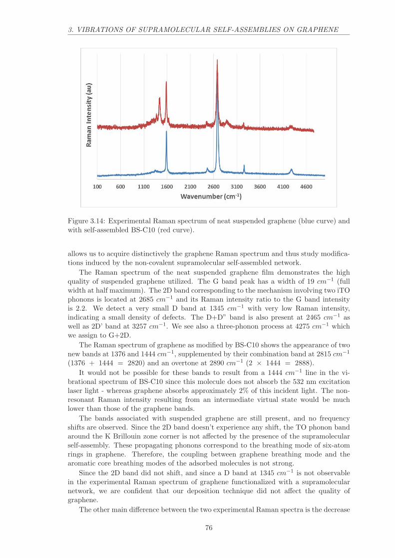
3. VIBRATIONS OF SUPRAMOLECULAR SELF-ASSEMBLIES ON GRAPHENE
Figure 3.14: Experimental Raman spectrum of neat suspended graphene (blue curve) andwith self-assembled BS-C10 (red curve).
allows us to acquire distinctively the graphene Raman spectrum and thus study modifica-tions induced by the non-covalent supramolecular self-assembled network.
The Raman spectrum of the neat suspended graphene film demonstrates the highquality of suspended graphene utilized. The G band peak has a width of 19 cm−1 (fullwidth at half maximum). The 2D band corresponding to the mechanism involving two iTOphonons is located at 2685 cm−1 and its Raman intensity ratio to the G band intensityis 2.2. We detect a very small D band at 1345 cm−1 with very low Raman intensity,indicating a small density of defects. The D+D” band is also present at 2465 cm−1 aswell as 2D’ band at 3257 cm−1. We see also a three-phonon process at 4275 cm−1 whichwe assign to G+2D.
The Raman spectrum of graphene as modified by BS-C10 shows the appearance of twonew bands at 1376 and 1444 cm−1, supplemented by their combination band at 2815 cm−1
(1376 + 1444 = 2820) and an overtone at 2890 cm−1 (2 × 1444 = 2888).
It would not be possible for these bands to result from a 1444 cm−1 line in the vi-brational spectrum of BS-C10 since this molecule does not absorb the 532 nm excitationlaser light - whereas graphene absorbs approximately 2% of this incident light. The non-resonant Raman intensity resulting from an intermediate virtual state would be muchlower than those of the graphene bands.
The bands associated with suspended graphene are still present, and no frequencyshifts are observed. Since the 2D band doesn’t experience any shift, the TO phonon bandaround the K Brillouin zone corner is not affected by the presence of the supramolecularself-assembly. These propagating phonons correspond to the breathing mode of six-atomrings in graphene. Therefore, the coupling between graphene breathing mode and thearomatic core breathing modes of the adsorbed molecules is not strong.
Since the 2D band did not shift, and since a D band at 1345 cm−1 is not observablein the experimental Raman spectrum of graphene functionalized with a supramolecularnetwork, we are confident that our deposition technique did not affect the quality ofgraphene.
The other main difference between the two experimental Raman spectra is the decrease
76

3. VIBRATIONS OF SUPRAMOLECULAR SELF-ASSEMBLIES ON GRAPHENE
Figure 3.15: Proposed mechanisms to explain the appearance of 1372 cm−1 and 1444 cm−1
bands in the experimental Raman spectrum. These mechanisms involve a TO phonon anda coupled graphene-adsorbed ”mambo mode”.
of the 2D/G ratio from 2.2 for neat suspended graphene to 1.3, when functionalizedby the supramolecular assembly. It is worth noting that the integration of the spectraover all frequencies gives exactly the same result for graphene alone and functionalizedgraphene. Consequently, the oscillator strength of the 2D band in the neat graphenespectrum appears as being transferred to the two new bands at 1376 and 1444 cm−1 inthe BS-C10 on graphene spectrum.
Since the G band intensity is not affected by the presence of the supramolecular self-assembly, the 2D band decrease is the sign that a new mechanism is competing with the2D mechanism, thus reducing the probability for the latter to occur. Since the only dif-ference between the two systems is the presence of the supramolecular network, and sinceno defects have been introduced by the deposition technique, the competing mechanismclearly involves the adsorbed molecules. The redistribution of the oscillator strength indi-cates a new Raman-active mode for graphene due to the presence of the supramolecularnetwork.
By breaking the translational invariance of the graphene lattice, vibrationally activemolecules on the graphene surface allow the optical excitation of D-band phonons withnon-zero wavevectors. They can then be seen as phonon launchers like localized defects.However, unlike structural defects, adsorbed molecules do not affect significantly graphenestructure. Thus, the vibrational coupling must be resonantly enhanced through the me-diation of a coupled vibration mode.
We demonstrated in previous sections that a molecule adsorbed on graphene can havevibrational mambo modes spatially delocalized on both graphene and the molecule. More-over, these modes have low frequencies typically in the range of 100 cm−1. This suggeststhat the 1376 and 1444 cm−1 bands in the experimental Raman spectrum results frommechanisms involving TO phonons and such mambo modes. These mechanisms are simi-lar to those producing the D band where the electronic wavevector conservation is ensuredduring the process of transforming photons into phonons by the fact that localized de-fects can compensate for any phonon wavevector. The only difference is the fact thatphonon defect modes are coupled at any frequency, whereas the mambo mode interactswith phonon modes at the given frequency of the involved coupled mode. We identifyelectron-hole, hole-electron, electron-electron intervalley scattering processes as principalmechanism producing the 1376 and 1444 cm−1 bands. These processes are displayed infigure 3.15.
Since the D band is not shifted (because the 2D band did not shift), according to
77

3. VIBRATIONS OF SUPRAMOLECULAR SELF-ASSEMBLIES ON GRAPHENE
this interpretation, the two new bands should involve two molecular mambo modes withfrequencies 101 cm−1 and 34 cm−1 as derived from the experimental spectrum. Suchorders of magnitude are consistent with DFT calculations of molecular mambo modeswhich predict resonant frequency on the order of 80 cm−1.
3.6 Conclusion
Adsorption on graphene offers a unique opportunity to apply resonance Raman spec-troscopy to fluorescent molecules, thanks to the fast quenching of molecular excited states.When self-assembled molecules on graphene interact with their substrate, the Van derWaals forces that allow the adsorption result from the overlapping of graphene sp2 orbitalswith either sp2 molecular orbitals or H atoms. Whereas these electronic interactions sig-nificantly perturb the electronic excited levels of the adsorbed molecule,122 the vibrationalproperties involving in-plane motions are kept almost intact. However, the presence ofthe graphene surface in the vicinity of such an adsorbed molecule gives rise to new out-of-plane low frequency molecule-graphene coupled vibrational modes. The frequencies ofsuch ”mambo mode” resonances are determined by the size of the adsorbed molecule andthe strength of the adsorption force, and are typically of the order of 100 cm−1 for aromaticmolecules. These findings open new perspectives in the engineering of graphene properties.The identification of mambo modes could be explored to build a bridge between visibleand IR optics, for example in optically triggering phonon launcher. More generally, ourwork emphasizes the capability, when engineering graphene-based self-assembled systems,to interrogate the nature of their adhesion to graphene through Raman spectroscopy.
78

Chapter 4
Plasmon engineering
Scanning electron microscope (SEM) image of nanoscale gold bowties measuring 240 nmlong and 170 nm large. (John Bigeon / C2N)
Metallic nanostructures have been used for centuries to produce colorful materials. Onecan cite the Lycurgus cup crafted in the Roman empire or the multitude of stained glasswindows decorating cathedrals. These structures have the ability to confine light at thenanoscale and thus very high electric field can be reached at their close vicinity. A deepunderstanding of how metallic nanostructures interact with light is needed depending ontheir shape, size, aggregation to extend today applications through the careful design ofsuch nanoscale objects and networks.
79

4. PLASMON ENGINEERING
Contents
3.1 Introduction to Raman scattering . . . . . . . . . . . . . . . . . 65
3.2 Graphene Raman spectrum . . . . . . . . . . . . . . . . . . . . . 67
3.3 DFT computations . . . . . . . . . . . . . . . . . . . . . . . . . . . 70
3.4 Resonant self-assembled monolayer on graphene . . . . . . . . . 72
3.5 Non-resonant self-assembled monolayer on graphene . . . . . . 75
3.6 Conclusion . . . . . . . . . . . . . . . . . . . . . . . . . . . . . . . 78
80

4. PLASMON ENGINEERING
4.1 Characteristics of plasmon modes
4.1.1 Rabi frequency
Surface plasmons polaritons are strongly coupled plasma electronic oscillations of a metalto the electromagnetic field of photons. They propagate at the metal surface. For asimple metal/dielectric interface, an analytic dispersion relation for the surface plasmoncan be obtained from the wave equation derived from Maxwell-Lorentz equation. A surfaceplasmon polariton can propagate if its wavevector β verifies the relationship:
β =ω
c
√
ǫmǫdǫm + ǫd
(4.1)
Where ǫm (resp.ǫd) is the dielectric constant of the metal (resp. the dielectric). Figure4.1 represents the dispersion relation of a surface plasmon polariton propagating at aninterface composed by vacuum and a Drude metal (plasma frequency ωp = 9eV ).
Figure 4.1: Dispersion relation of the plasmon polariton. Dashed lines represent thedispersion relation of a photon (called light line) and the dispersion relation of electronsin the metal (plasma frequency)
The lower branch of the polariton behaves like a photon at low frequency and tendsto ωp/
√2 at high frequencies. The upper branch of the polariton start from ωp at low
frequencies. The forbidden frequency gap between the upper and lower part of the polari-ton branches is the sign of an ultrastrong coupling.145,146 In this framework, the width, inenergy units, of the opened gap Eg can be linked to the coupling energy hωR
πthrough the
equation:
Eg =(hωR
π)2
2ωp(4.2)
Where ωR is the Rabi frequency describing the periodic energy exchange between thetwo coupled systems. The resolution of Maxwell equations plotted in figure 4.1 gives agap opening of 2.6 eV which correspond to a Rabi frequency ωR = 8.3 × 10¹⁴ s−1. Thisfrequency corresponds to a 360 nm wavelength photon propagating in free space. Energyexchanges between metal electrons and the electromagnetic field of the plasmon polaritonquasiparticle are then about two times faster than their oscillation frequencies, and willbe thus laid aside in the following.
81

4. PLASMON ENGINEERING
Figure 4.2: Field decay lengths from a gold/glass(n=1.5) interface inside the gold layer(left) and the vacuum layer (right). Gold permittivity were taken from Johnson andChristy.147
4.1.2 Field confinement and propagation length
Polarizability χ (or dielectric constant ǫ = 1+χ) properties of materials at the dielec-tric/metal interface dictate the characteristics of surface plasmon polariton: propagationlength, field extension above and below the interface. Figure 4.2 displays the decay lengthsof the fields from a gold/glass(n=1.5) interface inside the gold layer and the vacuum layer.
The plots in figure 4.2 show that such systems can confine electro-magnetic fields belowthe diffraction limit: for example, at a frequency corresponding to a 600 nm wavelengthphoton in free-space, the transverse decay length of the surface plasmon polariton field inthe glass layer is 100 nm.
However, a major drawback goes with this strong confinement of light in plasmonicsystems: electron motion in any metal is lossy due to Ohmic frictions that cause dampingof the plasma oscillations. Furthermore, at high frequencies, interband metal electronictransitions can also absorb electromagnetic energy thus further reducing the propagationlength of surface plasmon polaritons.
Figure 4.3 shows the propagation length of a surface plasmon polariton as a function ofits wavelength for a gold/glass(n=1.5) interface together with the corresponding dielectricconstant. As displayed by the imaginary part of the dielectric constant of gold, interbandtransitions prevent any propagation of the surface plasmon polariton below 500 nm. Above600 nm, The combination of low light absorption by gold and highly negative real partof the gold permittivity increases the surface plasmon polariton propagation length totenth of micrometers. Therefore practical uses of surface plasmon polaritons on gold arelimited to the red to near-infrared (NIR) range (600-800 nm). Actually, longer-wavelengthapplications, cheaper metals such as aluminum are workable.
Since lossy metals are unavoidable, losses are the principal limitation to applicationsof plasmonic cavities or waveguides. This has two main consequences. First, more effi-cient gain media are required to compensate for the losses and potentially produce gain.Second, losses constrain plasmonic resonators to poor quality factor and thus to ultra-fastrelaxation (typically 100 fs).
Since common gain media have a typical radiative lifetime of 1 ns, plasmonic laserscan be defined as class B lasers: the radiations are emitted by bursts.148
Further research on optical gain media is needed to engineer plasmonic propertiesaiming for a reduction of losses in such material.
82

4. PLASMON ENGINEERING
Figure 4.3: Real (long dash) and imaginary (short dash) part of the gold permittivitytaken from Johnson and Christy.147 Surface plasmon polariton propagation length at thegold/glass(n=1.5) interface.
4.1.3 Quality factor
The quality factor (Q-factor) is a practical figure to compare plasmonic resonators ofdifferent materials. It corresponds to the number of resonator oscillations before beingdamped. A quality factor for surface plasmon polariton Qspp and for a local nanostructureQloc can be defined:149
Qspp = − re(ǫ)
im(ǫ)(4.3)
Qloc =ω dre(ǫ)
dω
2im(ǫ)(4.4)
Qspp is the ratio of the propagation length to the wavelength of a SPP propagating atthe studied metal/vacuum interface. Qloc is the number of local plasmon oscillationsperformed by the resonator before being totally damped.
We compare in figure 4.4 the quality factors of silver and gold SPPs computed fromtheir experimental dielectric constant.147
Silver is known to have the best dielectric characteristics for visible plasmonics. Itshows relatively low losses and the real part of its dielectric permittivity is sufficientlynegative to end up with a good quality factor for the plasmonic resonance as shown infigure 4.4. However, the fast oxidation of any unprotected silver surface adds a techno-logical complication for plasmonic applications of silver. Therefore, gold represent a goodcompromise in terms of dielectric properties and technological manipulation. Compositematerials could be a strategy to engineer the dielectric properties and improve qualityfactor for local plasmon resonances or propagating surface plasmon polaritons.
4.2 Maxwell-Garnett materials
The Maxwell-Garnett approach aims at predicting the optical properties of an alloy thatcombines two materials. An effective dielectric constant ǫeff can be derived from the
83

4. PLASMON ENGINEERING
Figure 4.4: Qspp (crosses) and Qloc (no crosses) for silver (dash) and gold (plain) SPPs.Relative permittivity from Johnson and Christy.147
dielectric constant of matrix medium ǫm and inclusions ǫi knowing the volume fraction ofthe inclusions δi. This effective medium approximation assumes that inclusion domainsare spatially separated. This approach is thus expected to be valid at low volume fractions.The effective dielectric constant can be written:
ǫeff = ǫm2δi(ǫi − ǫm) + ǫi + 2ǫm2ǫm + ǫi + δi(ǫm − ǫi)
(4.5)
When the volume fraction is small, the effective dielectric constant has a pole for2ǫm + ǫi = 0. By considering a dielectric matrix with gold inclusions in the limit of lowvolume fractions, one retrieves the local plasmon resonance condition for gold nanospheresembedded in a dielectric matrix.
4.2.1 Glass inclusions.
An idea to reduce losses in a plasmonic material could consist in adding transparent inclu-sions which possibly would reduce the imaginary part of the plasmonic material relativelymore than its real part. Figure 4.5 displays effective dielectric constant and Qspp for agold matrix with glass (n=1.5) inclusions with volume fractions varying from 0 to 0.75.
The imaginary part of the composite medium dielectric constant is computed to belower than the pure gold medium case. However, the real part is more affected by thepresence of the inclusions, resulting in a lower quality factor for the composite mediumwhatever the wavelength. The quality factor can eventually be negative due to a positivereal part of the dielectric constant, meaning that the composite medium do not evendisplay a resonance.
4.2.2 Absorber inclusions.
A second idea that we tested was to use a typical absorber (Lorentzian resonator) asinclusions. Considering a dense packing (ρ = 1 molecule/(2nm)3) of PTCDI moleculeswith a σ = 3 × 10⁻²⁰ m2 absorption cross-section at resonance (530 nm), the imaginarypart of the absorber system dielectric constant is evaluated at resonance to:
Im(ǫr) =3cσρ
ω0= 6 (4.6)
84
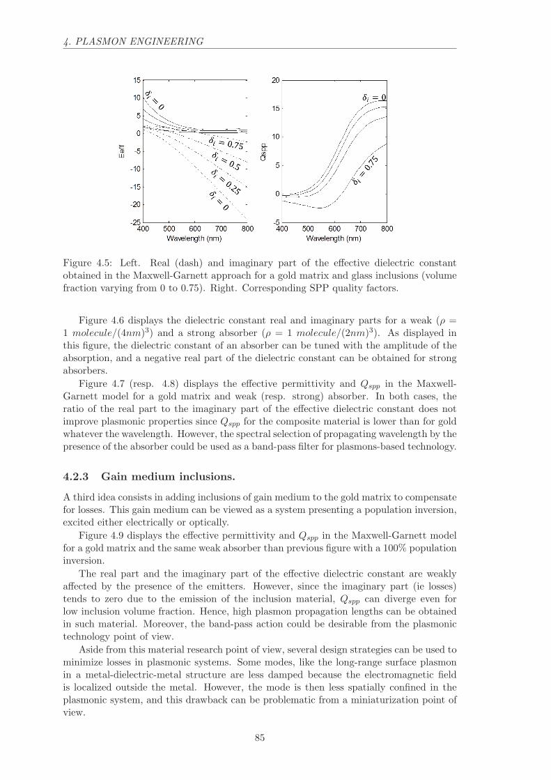
4. PLASMON ENGINEERING
Figure 4.5: Left. Real (dash) and imaginary part of the effective dielectric constantobtained in the Maxwell-Garnett approach for a gold matrix and glass inclusions (volumefraction varying from 0 to 0.75). Right. Corresponding SPP quality factors.
Figure 4.6 displays the dielectric constant real and imaginary parts for a weak (ρ =1 molecule/(4nm)3) and a strong absorber (ρ = 1 molecule/(2nm)3). As displayed inthis figure, the dielectric constant of an absorber can be tuned with the amplitude of theabsorption, and a negative real part of the dielectric constant can be obtained for strongabsorbers.
Figure 4.7 (resp. 4.8) displays the effective permittivity and Qspp in the Maxwell-Garnett model for a gold matrix and weak (resp. strong) absorber. In both cases, theratio of the real part to the imaginary part of the effective dielectric constant does notimprove plasmonic properties since Qspp for the composite material is lower than for goldwhatever the wavelength. However, the spectral selection of propagating wavelength by thepresence of the absorber could be used as a band-pass filter for plasmons-based technology.
4.2.3 Gain medium inclusions.
A third idea consists in adding inclusions of gain medium to the gold matrix to compensatefor losses. This gain medium can be viewed as a system presenting a population inversion,excited either electrically or optically.
Figure 4.9 displays the effective permittivity and Qspp in the Maxwell-Garnett modelfor a gold matrix and the same weak absorber than previous figure with a 100% populationinversion.
The real part and the imaginary part of the effective dielectric constant are weaklyaffected by the presence of the emitters. However, since the imaginary part (ie losses)tends to zero due to the emission of the inclusion material, Qspp can diverge even forlow inclusion volume fraction. Hence, high plasmon propagation lengths can be obtainedin such material. Moreover, the band-pass action could be desirable from the plasmonictechnology point of view.
Aside from this material research point of view, several design strategies can be used tominimize losses in plasmonic systems. Some modes, like the long-range surface plasmonin a metal-dielectric-metal structure are less damped because the electromagnetic fieldis localized outside the metal. However, the mode is then less spatially confined in theplasmonic system, and this drawback can be problematic from a miniaturization point ofview.
85
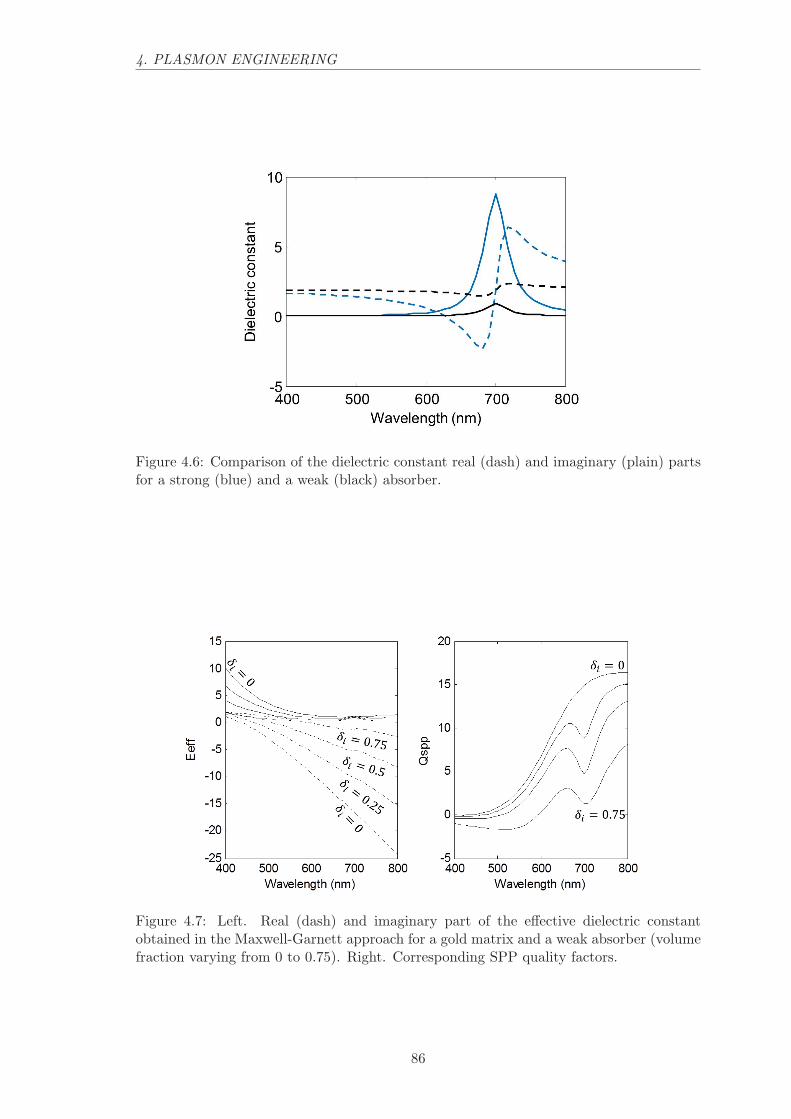
4. PLASMON ENGINEERING
Figure 4.6: Comparison of the dielectric constant real (dash) and imaginary (plain) partsfor a strong (blue) and a weak (black) absorber.
Figure 4.7: Left. Real (dash) and imaginary part of the effective dielectric constantobtained in the Maxwell-Garnett approach for a gold matrix and a weak absorber (volumefraction varying from 0 to 0.75). Right. Corresponding SPP quality factors.
86
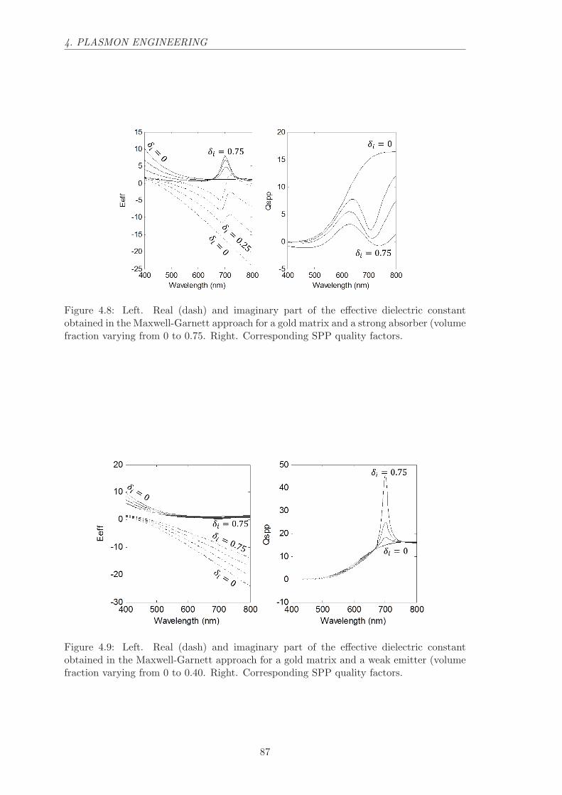
4. PLASMON ENGINEERING
Figure 4.8: Left. Real (dash) and imaginary part of the effective dielectric constantobtained in the Maxwell-Garnett approach for a gold matrix and a strong absorber (volumefraction varying from 0 to 0.75. Right. Corresponding SPP quality factors.
Figure 4.9: Left. Real (dash) and imaginary part of the effective dielectric constantobtained in the Maxwell-Garnett approach for a gold matrix and a weak emitter (volumefraction varying from 0 to 0.40. Right. Corresponding SPP quality factors.
87

4. PLASMON ENGINEERING
Figure 4.10: Description of the n-multilayer problem and notations.
4.3 Analysis of SPP dispersion relation
Engineering surface plasmon polaritons requires effective numeric and experimental toolsto simulate and characterize their physical properties: frequency, propagation length,field extension... Moreover, the experimental characterization should tackle the fact thatmost of the plasmon systems are very small, typically on the order of a few micrometersor less. Most of the critical information about surface plasmon polaritons is embeddedin the dispersion relation that results from solving Maxwell equation for this specificgeometry. For a simple gold/dielectric interface, an analytic dispersion relation for thesurface plasmon can be obtained. (cf. equation 4.1) However, analytic solution for thedispersion relation requires too complex calculations for a multilayer material.
Here we remind a numerical and an experimental tool to solve both numerically andexperimentally Maxwell equations, finding the dispersion relation of surface plasmon po-laritons at a precise spatial location (1 µm2 precision) on a plasmonic system.
4.3.1 Numerical dispersion relation.
The transfer matrix approach is usually used to compute the optical reflection and trans-mission of a multilayer material when a beam is incident its surface.150
Scheme 4.10 describes the multilayer problem composed of n homogeneous layerswith complex dielectric constant ǫi and extension Li normal to the interfaces (ie in thez-direction). In the following, we consider uniquely transverse magnetic (TM) incidentelectromagnetic fields.
The wavevector projection on the x-axis, β, is continuous through all interfaces for thewaves to propagate:
β = kp.x = kinc.x = kincsin(θinc) (4.7)
We then define kpz the projection along the z-axis of the complex wavevector of thelayer p:
kpz =√
k2p − β2 (4.8)
The TM propagating and counter propagating electric fields in the p layer can be deduced
88

4. PLASMON ENGINEERING
Figure 4.11: Reflection from a glass/gold (50 nm)/vacuum system as function of thewavelength and the incident angle of the incident electric field. Analytic dispersion relationfor a SPP propagating at a gold/vacuum interface (white line).
from those in the p-1 layer thanks to the Dp−1,p matrix derived from continuity equations:
Dp−1,p =1
2
[
1 + np−1,p 1− np−1,p
1− np−1,p 1 + np−1,p
]
(4.9)
np−1,p =ǫp−1
ǫp
kpzkp−1z
(4.10)
The propagation of the phase through the layer p of length Lp is carried out by thepropagation matrix Pp:
Pp =
[
exp(−ikpzLp) 00 exp(−ikpzLp)
]
(4.11)
We then write the overall matrix M that links the reflected and transmitted electricfield to the incident electric field:
[
Einc
Er
]
= M
[
Et
0
]
=
[
M11 M12
M21 M22
] [
Et
0
]
= D1,2P2...Dp−1,pPp...Dn−1,n
[
Et
0
]
(4.12)Reflected and transmitted fields and intensities can be deduced from the M matrix as
follows:
t =1
M11r =
M21
M11(4.13)
T =ǫ1ǫn
knzk1z
× tt∗ R = rr∗ (4.14)
Figure 4.11 displays the reflected intensity for a Kretschman configuration (glass /gold(50nm) / vacuum) as function of the wavelength and the incident angle of the incidentelectric field. Superposed to this figure is plotted in white the analytic dispersion relationfor a gold/vacuum interface in the ω − θ space.
A dip in the reflectivity appears above the total internal reflection angle at 41.8◦. At800 nm, this dip is located at 43◦ and this value increases as the wavelength decreases.This dip in the reflectivity is attributed to the coupling of the incident photon to thesurface plasmon mode. The analytic dispersion curve matches perfectly the reflectivity
89

4. PLASMON ENGINEERING
dip between 600 nm and 800 nm, validating our numerical implementation of the transfermatrix theory to compute the dispersion relation for more complex systems. Below 600 nm,the dip width increases due to gold interband transitions that shorten SPP propagationlength. This region also corresponds to the transition from plasmon polariton to photonpolariton, thus the analytic dispersion curve moves away from the reflectivity dip.Interestingly, intrinsic and radiative loss terms Γi and Γr for the propagating plasmonpolariton can be determined from the position, the height h and the width w of the dipby solving the following two equation system:151
h =4ΓiΓr
(Γi + Γr)2(4.15)
w =Γi + Γr
n2k0cos(θr)(4.16)
Where n2k0 is the incident wavevector onto the gold layer, and θr is the incident angleproducing the reflectivity dip.
The transfer matrix method is a simple to implement and effective tool to predict theposition in frequency and wavevector of the SPP mode. This figure permits to find theSPP wavelength from the wavector value of the reflectivity dip, and the SPP propagationlength from intrinsic and radiative loss terms extracted from the characteristics of thereflectivity dip.
4.3.2 Experimental dispersion relation
An incident beam with an important wavevector at a given frequency is needed to phase-match the plasmon polariton wavevector and thus excites it. In the Kretschman config-uration, the exciting beam is incident on the plasmonic waveguide coming from a prismat high angle of incidence. The plasmon polariton presence manifests itself by a dip inthe reflectivity signal at a given angle above the total internal reflection condition for theprism/air interface.
However, this method is not efficient to locally characterize the SPP properties. Weimplement a microscopy analogue of the Kretschman configuration that allows the charac-terization of SPP properties at the micro scale. Scheme 4.12 describes the experimentalset-up of the microscopy analogue of the Kretschman configuration. It is similar to theset-up used for example in ref.152
The prism in the traditional Kretschman configuration is replaced by the immersionoil of a high aperture objective. The reflected light is collected through the objective andanalyzed in the Fourier plane. Thus, reflected light is experimentally decomposed on awavevector basis. Moreover, the ability of the microscope objective to focus a collimatedincident beam onto the substrate allows characterizing it at a precise location, typicallywith several microns precision. Since Maxwell equations are decoupled in frequency, we canshine white light (Tungsten incandescent lamp in our setup) on the system to characterizeall frequencies at the same time knowing that the presence of multiple wavelengths willnot perturb the solution of the problem for one wavelength. For the same reason, wecan also send all wavevectors at the same time on the substrate. Since surface plasmonpolaritons are uniquely excited by an incident TM electromagnetic field, a broadbandpolarizer is placed after the white source. The experimental dispersion relation is obtainedby decomposing the reflectivity on a wavevector and a wavelength basis, as shown inthe previous section. The detection of the signal in the Fourier plane decomposes thereflectivity on a wavevector basis. Figure 4.13 displays images of the Fourier plane for areference glass sample and for 40 nm of gold deposited on top of this glass sample. A rough
90

4. PLASMON ENGINEERING
Figure 4.12: Description of the experimental set-up for obtaining the experimental SPPdispersion relation.
Figure 4.13: Experimental Fourier plane images obtained on a trichromatic camera witha linearly polarized white source illumination on a glass sample (a) and a glass samplecoated with 40 nm of gold (b).
spectral information is acquired at each pixel of the image using a simple trichromatic colorcamera.
The first image (a) displays simultaneously the TE and TM intensity reflection depen-dence on the incident angle along the vertical and horizontal image axes respectively fora glass/air interface. Brewster incidences are visible as dark spots on the TM axis whenthe incident wavector ki matches Brewster wavevectors ±kB. Above a certain incidentwavector kTIR, total internal reflection occurs and the light is entirely reflected by theglass/air interface. The coupling of the incident light to the surface plasmon polariton isvisible along the TM axis on the image (b), taken for the same glass sample coated with40 nm of gold. When ki matches ±kSPP , a dip in the reflection occurs. The white sourceallows obtaining very clear images since interference patterns are blurred by the presenceof multiple wavelength. However, the spectrum of the white source should be carefullyselected to see the dip in the reflectivity since it can be distorted for wavelength around500 nm and less.
A last step is needed to obtain the experimental dispersion relation. The decompositionof the reflectivity on a wavelength basis with a spectral resolution much better than thetrichromic camera is performed by scanning a multimode fiber linked to a spectrometer
91

4. PLASMON ENGINEERING
Figure 4.14: Experimental reflection from a glass sample coated with 40 nm of gold de-pending on the incident wavelength and angle with respect to the surface normal direction.
on the TM axis in the Fourier plane. The reflectivity function of the wavelength and thewavevector is then obtained by plotting spectra correlated to the position in the wavevectorspace. Figure 4.14 displays the intensity reflected by a glass sample coated with 40 nmof gold depending on the wavelength and angle with respect to surface normal directionof the incident electromagnetic waves.
The fiber has been scanned all along the TM axis in the Fourier plane, explainingthe symmetry of the figure. The dip in the reflectivity is clearly visible at high incidentangles. Saturated regions appear in the 550-400 nm range due to spectra normalization tothe normal incident angle spectrum. In fact, due to interband transitions the reflectivityis much less than 1 in the 400-550 nm range at normal incidence (cf figure 1.11). Thenumerical aperture of the microscope objective limits the wavevector range. This can beproblematic when a dielectric material is deposited on top of the gold layer, shifting theSPP band to higher wavevectors. Finally, the fiber entrance size limits the resolution onthe incident angle axis. A greater extension of the image in the Fourier plane is needed toget a more precise dispersion relation of the SPP.
This experimental technique is an efficient tool to characterize surface plasmon po-laritons properties and can be further calibrated with a diffraction grating for example toextract the dispersion relation of SPP.
4.4 High-Q plasmon modes
Engineering efficient plasmonic systems requires to carefully choose material. In the con-text of plasmonic cavities, one may wonder what geometry to adopt for the nanoparticle inorder to maximize the quality factor of the plasmon resonance. For a single nanoparticle,the resonance frequency depends on the fraction of the plasmon energy inside the metal,and for this specific frequency the quality factor of the resonance is determined only bythe complex dielectric function of the metal.153
However, electromagnetic interactions between individual units can be exploited todecrease internal metal losses and obtain high quality factor resonances.154 The transitionfrom a mode localized on a single nanoparticle to a Bloch mode delocalized on multiplenanoparticle changes the fraction of the plasmon energy inside the metal, and may leadto a high-Q plasmon mode.
In the following, we compute the quality factor of a nanorod and observe how it evolves
92

4. PLASMON ENGINEERING
Figure 4.15: Gold nanorod with airgap on a glass substrate used for computations.
when a gap is opened in the middle of the nanorod. Scheme 4.15 displays the geometryof the rod and the gap varying from 0 to 5 nm.
We use the RETICOLO code, an implementation of a frequency-domain modal methodknown as the Rigorous Coupled Wave Analysis (RCWA) to compute the optical absorptionof nanorods. Since it computes diffraction efficiencies and diffracted amplitudes of grat-ings composed of stacks of lamellar structures, we use perfectly matched layers to isolatenanoparticles from nearest neighbors. We also use a Granet transformation155 to increasespatial resolution around permittivity function discontinuities and improve convergencerates.
Figure 4.16 displays the absorption spectra of a nanorod with an air gap varying from0 to 5 nm. As the gap between the two rods increases, several effects are observed. First,the absorption resonance shifts toward the blue. The gap produces a consequent reductionof the nanorod aspect ratio. However, the reduction of the aspect ratio by a factor 2 iscompensated by the in-phase coupling of the two rods that shifts the resonance to the redin a similar manner than J-aggregates.
Second, the absorption band decreases. This can be understood by the reduction ofthe number of electrons participating in the mode, therefore reducing the mode oscillatorstrength. Finally, a clear increase of the local plasmon resonance quality factor occurswhen the gap increases, as displayed in 4.4. High quality factor plasmon resonances cantherefore be obtained using in-phase coupling of small dipoles. A delocalized collectivemode displaces the fraction of plasmon energy from metal to the dielectric environment.
Gap (nm) 0 1 2 3 4 5
Qloc 14.3 16.5 17.5 18.9 22.1 23.9
A new resonance around 550 nm, not displayed in figure 4.16, appears as the gapincreases. We assign this mode to the gap mode.
Opening gaps in a nanorod is an effective approach to obtain relatively high qualityfactors thanks to collective modes that are create by the in-phase coupling of small dipoles.However, opening 5 nm gaps in small nanorods seems unrealistic for the today availabletechnology. One can draw a parallel with near-field dipole coupling in J-aggregates wherethe in-phase coupling of dye molecules creates an exciton mode delocalized on severalmolecules that displays a red-shifted resonance frequency with a smaller bandwidth andhigher oscillator strength.
93

4. PLASMON ENGINEERING
Figure 4.16: Gold nanorod absorption spectra when varying gap from 0 nm to 5 nm.
4.5 Conclusion
The electron damping in metals is the major issue in plasmonics for most of applications.Material research is needed to find ways to overcome or avoid these losses. We show thatthe Maxwell-Garnet and the Matrix transfer method are two useful theoretical approachesto conveniently predict exotic material dielectric properties and associated plasmon po-lariton characteristics. We experimentally demonstrate the possibility to measure thedispersion relation of plasmon polaritons. Finally, we show that the in-phase coupling ofnano-rods can increase the quality factor of a local plasmon resonance, which is desiredfor example to amplify this mode through the interaction with emitters.
94
Chapter 5
Strongly coupled self-assembled
dyes and plasmons
Back focal plane of the fluorescence from a self-assembled PTCDI-C7 thin film coupledto surface plasmon polaritons propagating at the gold surface.
The coupling between the dye molecules and the plasmon mode results in the dye emittingmost of the light at a specific angle.
95

5. STRONGLY COUPLED SELF-ASSEMBLED DYES AND PLASMONS
Contents
4.1 Characteristics of plasmon modes . . . . . . . . . . . . . . . . . . 81
4.1.1 Rabi frequency . . . . . . . . . . . . . . . . . . . . . . . . . . . . 81
4.1.2 Field confinement and propagation length . . . . . . . . . . . . . 82
4.1.3 Quality factor . . . . . . . . . . . . . . . . . . . . . . . . . . . . . 83
4.2 Maxwell-Garnett materials . . . . . . . . . . . . . . . . . . . . . . 83
4.2.1 Glass inclusions. . . . . . . . . . . . . . . . . . . . . . . . . . . . 84
4.2.2 Absorber inclusions. . . . . . . . . . . . . . . . . . . . . . . . . . 84
4.2.3 Gain medium inclusions. . . . . . . . . . . . . . . . . . . . . . . . 85
4.3 Analysis of SPP dispersion relation . . . . . . . . . . . . . . . . 88
4.3.1 Numerical dispersion relation. . . . . . . . . . . . . . . . . . . . . 88
4.3.2 Experimental dispersion relation . . . . . . . . . . . . . . . . . . 90
4.4 High-Q plasmon modes . . . . . . . . . . . . . . . . . . . . . . . . 92
4.5 Conclusion . . . . . . . . . . . . . . . . . . . . . . . . . . . . . . . 94
96

5. STRONGLY COUPLED SELF-ASSEMBLED DYES AND PLASMONS
The coupling between light and matter allows controlling excited state radiative life-time and spatial light emission patterns, to change the dynamics from incoherent to co-herent, to create strongly non-linear systems active at low intensities. Such propertieslead to the realization of single photons sources,156 ultra-low threshold lasers,157 photonblockade,158 ultrafast all-optical switches.159 All of these devices operate in the strongcoupling regime where the interaction between an emitter and a specific electromagneticmode dominates over the other interactions such as the interaction between the emitterand the continuum of vacuum modes.
Plasmonics exhibits several advantages for the realization of such components oper-ating under strong coupling conditions. First, nano-fabrication techniques of plasmonicwaveguides such as physical vapor deposition nanopatterning of gold are well known andcontrolled. Second, metal electrons confine electromagnetic modes at the metal surface.Since the dipole-photon coupling scales with the field-confinement volume V as
√
1/V ,160
plasmon modes can demonstrate very high coupling constants to dipoles up to the ultra-strong coupling regime.161 Last, plasmonic systems coupled to organic dyes and quantumdots have demonstrated strong-coupling regime at room temperature proving the possi-bility to develop optical quantum devices operating under ambient conditions.162,163,164
Among all organic dye systems, dye aggregates are especially interesting since co-herence effects between neighbor dyes resulting from intermolecular strong coupling canincrease the dye system oscillator strength f at resonance. In such coherent collectiveexcitations, the dipole moment scales as
√N where N represents the number of interact-
ing dye molecules. Since the dipole-photon coupling scales as√f , collective excitations
favor the strong coupling regime, in particular when coupled to a plasmonic waveguide.165
However, this√N factor does not impact the strength of the coupling when exciting the
molecules, since the same phase is imposed to all the molecules by the excitation field.Depending on the orientation and the distances between the molecules within the aggre-gate, the collective excitation sees its resonance shifting toward higher (H-aggregate) orlower (J-aggregate) frequencies with respect to the isolated dye.
Therefore, the optimization of the interaction between a plasmonic mode and a dyesystem requires a precise control over intermolecular interactions inside the dye layer andthus their relative positioning and orientations. Furthermore, the precise positioning ofdyes is also needed to increase the spatial and orientational overlap between dye dipolesand the plasmon mode electric field distribution and orientation: since the electric fieldof a plasmon polariton propagating at a metal surface is mainly normal to the surface,vertically oriented dye dipoles could further increase the interaction. In the meantime, theelectric field of the plasmon polariton mode decays exponentially from the metal surface.Thus dye dipoles should be placed close to the surface to maximize the dye-plasmoninteractions.
As a bottom-up approach, molecular self-assembly is the ultimate tool to control thearrangement of dye molecules with reference to each other. Furthermore, the molecularself-assembly approach also allows controlling the positioning of the assembled moleculewith reference to the substrate surface, and vertically aligned molecules on top of a sub-strate can be obtained as demonstrated in chapter 1. Finally, the very high density ofmolecules in such systems confine photonic responsive elements in an extremely thin layerthat is required to optimize the spatial overlap with the plasmon polariton mode.
Consequently, the self-assembly approach opens interesting prospects for the optimiza-tion of plasmon-organic dye coupling at the nanometer scale aiming at the developmentof optical quantum devices working under ambient conditions.
In this chapter, the coupling between a plasmon polariton mode propagating at agold surface and a self-assembled N,N’-diheptyl-3,4,9,10-perylenedicarboximide (PTCDI-C7) thin film deposited by molecular beam epitaxy on top of the gold layer is studied.
97

5. STRONGLY COUPLED SELF-ASSEMBLED DYES AND PLASMONS
The dispersion relation of this hybrid system is modeled numerically and characterizedexperimentally by probing the system reflectivity coefficient dependence on incidence an-gle and wavelength of an incident beam. The strong coupling regime is experimentallydemonstrated. The emission is also investigated by leakage radiation microscopy and bynumerical computations to clarify light-matter interactions with emitters displaying largeStokes shift.
5.1 Anti-crossing in self-assembled PTCDI on gold systems
Two oscillators can periodically exchange energy if they are interacting. This phenomenoncan manifest itself in the framework of electromagnetic modes couplings principally at thecrossing of the two systems dispersion relation curve, where the two systems are resonantin both frequency and wavevector domains. If the coupling is strong enough, the frequencyat which the two systems exchange energy - called Rabi frequency - is large enough toremove the degeneracy of the two interacting states beyond their natural line widths. Ahigh and a low energy coupled modes are then created corresponding to the two oscillatorsbeing either in-phase or out-of-phase. This results in an anti-crossing of the two oscillatorsystem dispersion relation lines that is usually considered as a proof for strong coupling.An pedagogical detailed explanation of strong coupling in dye-surface plasmon polaritonsystems can be found in reference.164
In the previous chapter, the determination of the numerical and experimental dis-persion relation of a plasmonic system has been presented. In the following, these twotechniques will be used to give an insight into strong coupling between a dye thin film ontop of a 40 nm thick gold film.
5.1.1 Tuning the Rabi frequency
The dielectric permittivity of the dye thin film is modeled as a lorentzian oscillator.Theimaginary part is fitted from a transmission absorption measurement at normal incidencethrough the dye thin film. For example, a 30 nm thick PTCDI-C7 thin film absorbs ∼ 30%of the incident light at resonance, as shown in chapter 1. The real part is then computedalong Kramers-Kronig principle to obtain an off-resonant real part of the refractive indexaround 1.4, which corresponds to dense π-conjugated molecular medias. Dye dipoles insidethe thin film are considered to be isotropically distributed.
Figure 5.1 displays the dispersion relation computed for a 30 nm thick dye thin filmon top of a 40 nm thick gold layer. To get insight into the specific role of the real andimaginary parts of the dye dielectric constant in the coupling to plasmons polaritons,the real part of the dye thin film dielectric constant has been set to the constant valueof 1.42 in figure 5.1 a), the imaginary part of the dye thin film dielectric constant hasbeen set to zero in figure 5.1 b), and both real and imaginary parts of the dye thin filmdielectric constant are regularly implemented in the simulation in figure 5.1 c). Noticethat Kramers-Kronig relations are not verified anymore for the dielectric constant used inthe two figures 5.1 a) and b), and thus does not represent a possible real physical system.
The presence of a dye layer with a uniform dielectric constant real part on top ofthe gold layer (figure 5.1 a)) changes the plasmon polariton dispersion relation in threeways. First, the reflectivity drop is uniformly shifted to higher wavectors. This resultsdirectly from the presence of a higher refractive index material on top of gold. Second,the reflectivity drop is enlarged in the wavevector direction close to the dye absorptionband, for example at 700 nm.
Last, and more surprisingly, the drop in the reflectivity is reduced by a factor 10 fromR = 0.03 for a gold/air interface to R = 0.3 for the gold/dye/air interface. One could
98

5. STRONGLY COUPLED SELF-ASSEMBLED DYES AND PLASMONS
Figure 5.1: Calculated Reflection from a glass/gold (40 nm)/Absorber dye thin film (30nm)system as function of the wavelength and the incident angle of the incident electric field.a): Re(ǫdye) set to 1.9, Im(ǫdye) left unchanged . b): Re(ǫdye) left unchanged, Im(ǫdye)set to 0. c): No modification of ǫdye.
have expected to increase the reflectivity drop since more absorption occurs in the systemwith the addition of the absorbing layer (A = 30% for the dye layer at normal incidence).This is true if one integrates the reflectivity coefficient over wavevectors. However, since thereflectivity drop is significantly broadened by the dye absorption that shortens the plasmonpolariton propagation length, the reflectivity drop peak is more important without thanwith the absorbing layer. From another point of view, the absorption is such that plasmonspolaritons can’t propagate and do not exist at this wavevector.
The presence of a dye layer with a null dielectric constant imaginary part on top ofa gold layer is displayed in figure 5.1 b). Apart from a global shift to higher wavevec-tors produced by a high mean refractive index, the plasmon polariton dispersion relationdisplays an interesting feature around the dye resonant frequency. The variation of therefractive index function of the frequency due to the dye resonance is directly imprintedon the wavevector position of the reflectivity drop since this position is given by the valueof the refractive index. This result can be derived from the analytical plasmon polaritondispersion relation at the interface between gold and a dye medium having both an infinitespatial expansion:
β = k0
√
ǫmǫdyeǫm + ǫdye
(5.1)
If Im(ǫdye) = 0 and if Re(ǫdye)− 1 ≪ Re(ǫm) then the above equation can be rewritten:
β = ndye(λ)2π
λ
√
ǫmǫm + 1
(5.2)
Figure 5.1 c) displays the reflection coefficient for the glass/gold (40nm)/ absorberdye thin film (30 nm) system with a dye dielectric constant complying with the Kramers-Kronig relation. This numerical simulation can be viewed as the combination of the twoprevious unphysical special cases. The real part of the dye dielectric constant is responsiblefor the position of the reflectivity drop in the 2D wavevector-wavelength space, whereasthe imaginary part governs absorption and thus the reflection drop width and height. Atdye resonance wavelength, the dye absorption is too strong to allow the propagation ofsurface plasmon polaritons and thus create the anti-crossing characteristic shape of thedispersion relation.
Since the anti-crossing strongly depends on the refractive index, one can control theenergy exchange rate between systems through the choice of the proper refractive index.For example, figure 5.2 displays the dispersion relation of plasmon polaritons for a dyeabsorber thin film composed of either one resonator (figure 5.2 center) or two resonators
99

5. STRONGLY COUPLED SELF-ASSEMBLED DYES AND PLASMONS
Figure 5.2: Left. Considered real and imaginary part of a one (black) and two (blue)absorber thin film dielectric constant. Calculated reflection coefficient from a glass/gold(40nm)/dye (30nm)/vacuum system where the dye medium correspond to the black (center)and the blue (right) dielectric constant.
(figure 5.2 right) having close eigenfrequencies (figure 5.2 left). The anti-crossing in thetwo resonator system is much larger than for the one resonator system. Therefore, it ispossible to tune the value of the opened gap Eg by acting on the difference between thenatural frequencies of the two oscillators.
5.1.2 Experimental evidence of anti-crossing
A 30 nm thick PTCDI-C7 thin film is deposited on a 30 nm gold layer on a SiO2 sub-strate. AFM measurements, together with absorption and fluorescence spectra of thisself-assembled PTCDI-C7 layer are detailed in chapters 1 and 2. Figure 5.3 a) displaysthe experimental reflection coefficient of TM polarized light incident on the system fromthe SiO2 side in a leakage radiation microscopy setup (see section 4.3), depending on thewavelength and the incidence angle of this incident light. The maximal incidence angleθmax = 74.5◦ is fixed by the numerical aperture of the immersion objective, which cor-responds here to NA = 1.46. A matrix transfer method simulating the experiment isdisplayed in figure 5.3 b). The absorption is modeled as a Lorentzian oscillator centeredat λmax = 565 nm with a 40 nm width (FWHM). The off-resonance refractive index isset to 1.6. For the simulation we assumed an isotropic orientational distribution of dyedipoles which is not the case in the real system, as shown in chapter 1.
Experimental data clearly show two branches of low reflectivity, symbolized by theblack dots on the figure. The anticrossing wavelength (∼ 565 nm) corresponds to thetransition from the ground HOMO state to a Frenkel excitonic state delocalized on severaldye molecules (0-F transition), sometimes considered as a hybrid charge-transfer Frenkelexciton. The anti-crossing width is measured to be 110 meV which is comparable withvalues reported for J-aggregates in other plasmonics systems.164 The numerical simula-tion retrieves quite accurately the experimental reflectivity. It is interesting to note thatplasmon polaritons couple with excitonic states delocalized on several dye units, creatinga polariton which mixes plasmon propagating on gold and delocalized Frenkel excitons.
5.2 Luminescence of self-assembled PTCDI on gold
5.2.1 Strong coupling and Stokes shift
In the previous section, the dyes have been considered to be driven by an exciting electro-magnetic field. In a two-state model, dyes emit the absorbed light at the same frequency.However, most of dyes molecules can’t be considered as two state systems since they dis-play a difference between band positions of the absorption and emission spectra. This
100
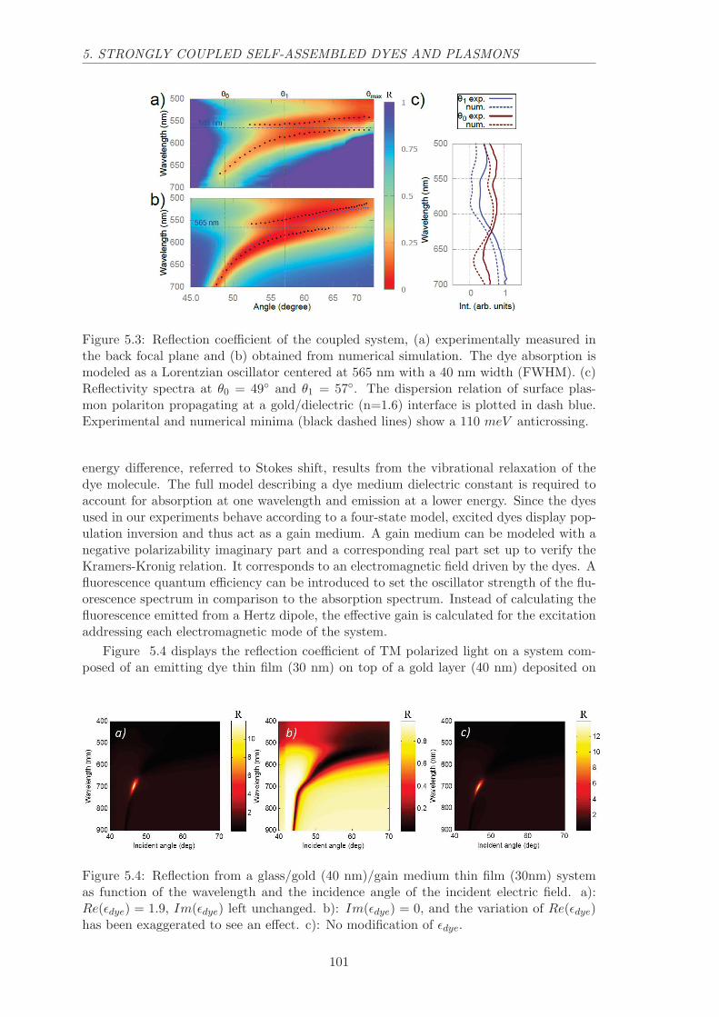
5. STRONGLY COUPLED SELF-ASSEMBLED DYES AND PLASMONS
Figure 5.3: Reflection coefficient of the coupled system, (a) experimentally measured inthe back focal plane and (b) obtained from numerical simulation. The dye absorption ismodeled as a Lorentzian oscillator centered at 565 nm with a 40 nm width (FWHM). (c)Reflectivity spectra at θ0 = 49◦ and θ1 = 57◦. The dispersion relation of surface plas-mon polariton propagating at a gold/dielectric (n=1.6) interface is plotted in dash blue.Experimental and numerical minima (black dashed lines) show a 110 meV anticrossing.
energy difference, referred to Stokes shift, results from the vibrational relaxation of thedye molecule. The full model describing a dye medium dielectric constant is required toaccount for absorption at one wavelength and emission at a lower energy. Since the dyesused in our experiments behave according to a four-state model, excited dyes display pop-ulation inversion and thus act as a gain medium. A gain medium can be modeled with anegative polarizability imaginary part and a corresponding real part set up to verify theKramers-Kronig relation. It corresponds to an electromagnetic field driven by the dyes. Afluorescence quantum efficiency can be introduced to set the oscillator strength of the flu-orescence spectrum in comparison to the absorption spectrum. Instead of calculating thefluorescence emitted from a Hertz dipole, the effective gain is calculated for the excitationaddressing each electromagnetic mode of the system.
Figure 5.4 displays the reflection coefficient of TM polarized light on a system com-posed of an emitting dye thin film (30 nm) on top of a gold layer (40 nm) deposited on
Figure 5.4: Reflection from a glass/gold (40 nm)/gain medium thin film (30nm) systemas function of the wavelength and the incidence angle of the incident electric field. a):Re(ǫdye) = 1.9, Im(ǫdye) left unchanged. b): Im(ǫdye) = 0, and the variation of Re(ǫdye)has been exaggerated to see an effect. c): No modification of ǫdye.
101

5. STRONGLY COUPLED SELF-ASSEMBLED DYES AND PLASMONS
Figure 5.5: Reflection from a glass/gold (40 nm)/dye thin film (30nm) system as functionof the wavelength and the incident angle of the incident electric field. The dye thin filmabsorbs light around 600 nm and fluoresces around 700 nm with a fluorescence quantumyield of 32% (left) and 38% (center).Right: Signal integration over wavevectors for left(plain) and right (dashed) figure.
SiO2. To get an insight into processes at play, Re(ǫdye) is considered constant in Figure5.4 a). It can thus not be considered as a physical system. Far from the dye resonance, nochange in the SPP reflectivity drop is observed. At wavelengths close to the dye resonance,this simulation shows that most of the fluorescence signal of the dye layer is concentratedat the reflectivity drop wavevector position. In other words, the dyes of the gain mediummainly decay into the surface plasmon polariton mode.
In figure 5.4 b), Im(ǫdye) has been set to zero and the variation of Re(ǫdye) hasbeen exaggerated to clearly identify the plasmon polariton dispersion curve dependenceon the refractive index change. Instead of flattening the dispersion relation curve alonga β = βresonance line as it is the case for an absorbing layer, the presence of the gainmedium flattens the dispersion relation curve along a λ = λresonance line. Since thegain medium layer drives the electromagnetic field, its polarization is ahead of phase incomparison to the field at low frequency. On the other hand, if the dye layer is absorbingthe electromagnetic field, its polarization is delayed at low frequency. Therefore, dye layerrefractive index variations as function of the frequency are inverted between the absorbingand the emitting case.
The refractive index variation of an gain medium thin film has the effect of increas-ing the density of plasmon polariton states at resonance wavelength but decreases thelocalisation of the polariton in the wavevector space.
Figure 5.4 c) displays the reflectivity with a physical ǫdye. The resulting figure is acombination of the effects described in the two previous paragraphs. Very high exciteddye densities are required to see a modification of the dispersion relation curve. The maineffect is the dye radiative decay into the SPP mode.
In the following, the dye thin film absorbs light around 600 nm and fluoresces at 700nm to account for the Stokes shift with a 20% fluorescence quantum yield. Figure 5.5displays the reflection coefficient of incident TM polarized electromagnetic waves on asystem composed of a dye thin film (30 nm) on top of a gold layer (40 nm) deposited onSiO2.
In this case absorption and emission resonances are significantly separated in the fre-quency domain. The overall behavior of the system is a combination of the two previoussections. Below 650 nm, the anti-crossing is visible in the reflection of the exciting elec-tromagnetic field. Above, 650 nm, the gain medium layer mainly excite the field in thesurface plasmon polariton mode.
Thus, the Stokes shift major effect is to shift the emission from the anticrossing fre-quency resulting in a coupling of the gain medium to plasmon polaritons that are unper-turbed by the absorption of the dyes.
102

5. STRONGLY COUPLED SELF-ASSEMBLED DYES AND PLASMONS
An increase of the fluorescence quantum efficiency from 32% to 38% leads to a rapidaugmentation of the fluorescence signal from 65 to 250, as shown in figure 5.5, goingwith a reduction of the fluorescence peak bandwidth from 45 nm to 30 nm. This directlyresults from the increase of the polariton propagation length that reduces the mode band-width. Ultimately, when the dye fluorescence compensates plasmon losses at the peak dyefluorescence wavelength, the polariton can propagate infinitely at this wavelength and thefluorescence signal tends to infinity.
5.2.2 Experimental wavevector resolved luminescence spectra
Experimental wavevector resolved emission spectra are taken by exciting the self-assembledPTCDI-C7 thin film on top of the gold layer with a 532 nm continuous wave laser (1 mWpumping power on a ∼ 1 µm2 surface), collecting light by the SiO2 side of the samplethrough the immersion objective. The spectra are displayed in figure 5.6. Simultane-ously, matrix transfer simulations are performed to model the experimental wavevectorresolved data. From an experimental fluorescence spectrum at low fluence the PTCDI-C7spectrum is modeled with two bands at 625 nm and 680 nm with an equivalent width.The absorption of a 30 nm thick PTCDI-C7 thin film is set to 30% in transmission, asmeasured in a transmission absorption measurement. The mean refractive index is set to1.6. Finally, we consider a 10% radiative quantum yield.
The computed reflection coefficient resolved in wavelength and wavevector for the dyelayer, which refractive index displays both absorption and fluorescence, shows a dip inthe reflection along the surface plasmon polariton mode and an enhanced reflection at thecrossing between the plasmon dispersion curve and the dye layer fluorescence frequency.The matrix transfer method requires the multi-layer system to be excited by an incidentfield that will reveal the dip in the reflection coefficient corresponding to the plasmon dis-persion relation. This is not the case in the experimental wavevector resolved luminescencespectra because the gain medium is excited by a laser beam coming from the top of thesystem. Therefore, we implemented the following procedure to keep only the signatureof the enhanced reflection produced by the emission of the gain layer in the computedreflection coefficient.
The enhanced reflection coefficient is obtained when the reflection coefficient computedwithout any fluorescence (Im(ǫdye) = 0, Re(ǫdye) left unchanged) is subtracted from thereflection coefficient computed with the full dye layer dielectric characteristics.
It is worth noting that this procedure implies an in-phase emission of all emitters inthe dye medium layer, which is questionable in the experiment.
The experimental wavevector resolved emission spectra in figure 5.6 show a clearconcentration of the emission at a certain wavevector corresponding to an angle of ∼ 49◦.The superposition of the dispersion relation for the unexcited coupled plasmon polariton-dye system shows that the emission concentrates into the plasmon polariton mode. Belowand above this resonance wavevector, two dye fluorescence bands can be identified at610 nm and 680 nm. These bands correspond to the fluorescence of the PTCDI-C7 thinfilm on SiO2.
The matrix transfer simulation is in fair agreement with the experimental data. Theemission is mainly detected in the plasmon polariton mode. Emission is also detected abovethe plasmon polariton wavevector. However, the computed signal for these wavevectors issignificantly smaller than the experimental signal. This could result from a mismatch inthe definition of the dye layer due to the anisotropy of the experimental system that thesimulation does not take into account.
103
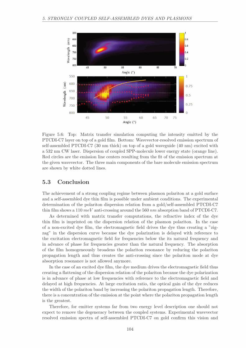
5. STRONGLY COUPLED SELF-ASSEMBLED DYES AND PLASMONS
Figure 5.6: Top: Matrix transfer simulation computing the intensity emitted by thePTCDI-C7 layer on top of a gold film. Bottom: Wavevector-resolved emission spectrum ofself-assembled PTCDI-C7 (30 nm thick) on top of a gold waveguide (40 nm) excited witha 532 nm CW laser. Dispersion of coupled SPP-molecule lower energy state (orange line).Red circles are the emission line centers resulting from the fit of the emission spectrum atthe given wavevector. The three main components of the bare molecule emission spectrumare shown by white dotted lines.
5.3 Conclusion
The achievement of a strong coupling regime between plasmon polariton at a gold surfaceand a self-assembled dye thin film is possible under ambient conditions. The experimentaldetermination of the polariton dispersion relation from a gold/self-assembled PTCDI-C7thin film shows a 110meV anti-crossing around the 560 nm absorption band of PTCDI-C7.
As determined with matrix transfer computations, the refractive index of the dyethin film is imprinted on the dispersion relation of the plasmon polariton. In the caseof a non-excited dye film, the electromagnetic field drives the dye thus creating a ”zig-zag” in the dispersion curve because the dye polarization is delayed with reference tothe excitation electromagnetic field for frequencies below the its natural frequency andin advance of phase for frequencies greater than the natural frequency. The absorptionof the film homogeneously broadens the polariton resonance by reducing the polaritonpropagation length and thus creates the anti-crossing since the polariton mode at dyeabsorption resonance is not allowed anymore.
In the case of an excited dye film, the dye medium drives the electromagnetic field thuscreating a flattening of the dispersion relation of the polariton because the dye polarizationis in advance of phase at low frequencies with reference to the electromagnetic field anddelayed at high frequencies. At large excitation ratio, the optical gain of the dye reducesthe width of the polariton band by increasing the polariton propagation length. Therefore,there is a concentration of the emission at the point where the polariton propagation lengthis the greatest.
Therefore, for emitter systems far from two energy level description one should notexpect to remove the degeneracy between the coupled systems. Experimental wavevectorresolved emission spectra of self-assembled PTCDI-C7 on gold confirm this vision and
104

5. STRONGLY COUPLED SELF-ASSEMBLED DYES AND PLASMONS
show a clear concentration of the emission into the polariton mode.
105

5. STRONGLY COUPLED SELF-ASSEMBLED DYES AND PLASMONS
106
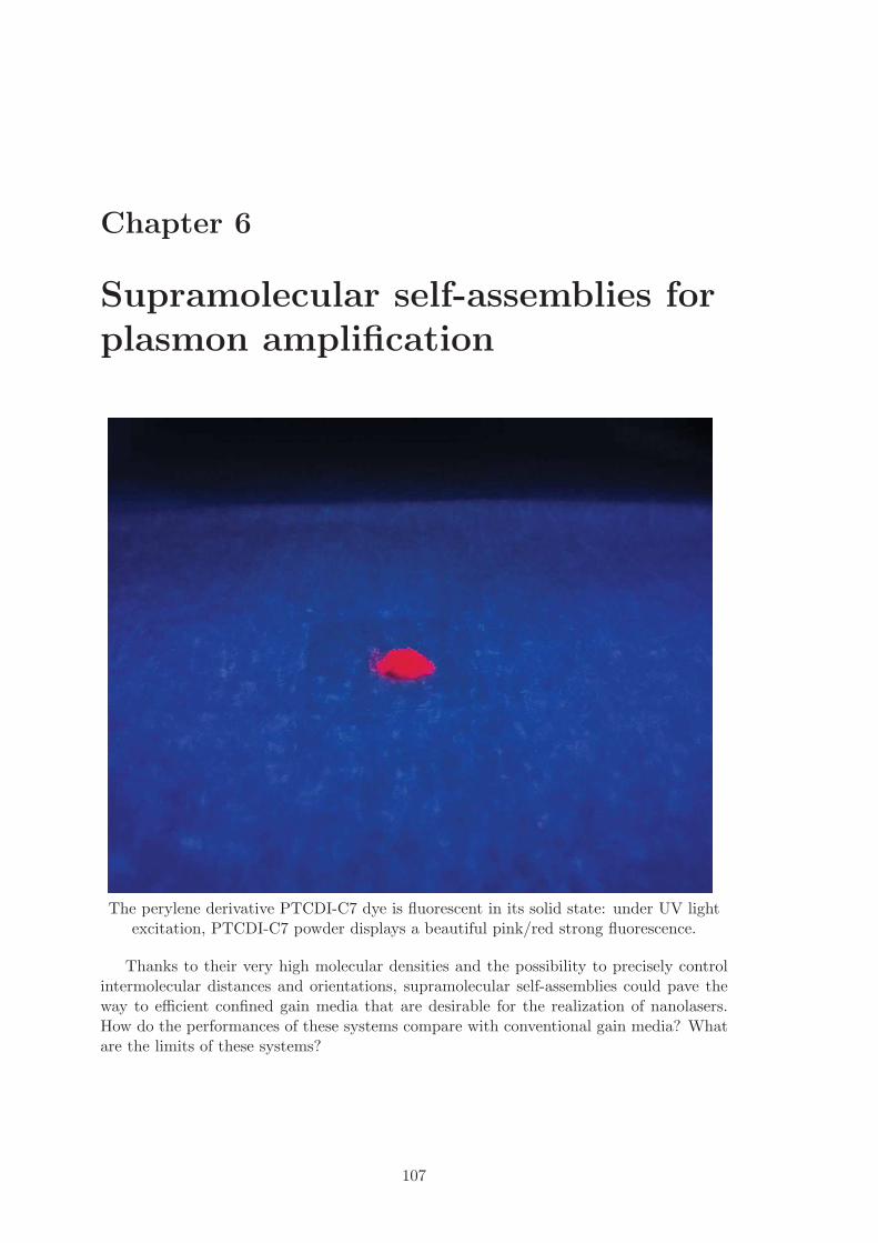
Chapter 6
Supramolecular self-assemblies for
plasmon amplification
The perylene derivative PTCDI-C7 dye is fluorescent in its solid state: under UV lightexcitation, PTCDI-C7 powder displays a beautiful pink/red strong fluorescence.
Thanks to their very high molecular densities and the possibility to precisely controlintermolecular distances and orientations, supramolecular self-assemblies could pave theway to efficient confined gain media that are desirable for the realization of nanolasers.How do the performances of these systems compare with conventional gain media? Whatare the limits of these systems?
107

6. SUPRAMOLECULAR SELF-ASSEMBLIES FOR PLASMON AMPLIFICATION
Contents
5.1 Anti-crossing in self-assembled PTCDI on gold systems . . . . 98
5.1.1 Tuning the Rabi frequency . . . . . . . . . . . . . . . . . . . . . 98
5.1.2 Experimental evidence of anti-crossing . . . . . . . . . . . . . . . 100
5.2 Luminescence of self-assembled PTCDI on gold . . . . . . . . . 100
5.2.1 Strong coupling and Stokes shift . . . . . . . . . . . . . . . . . . 100
5.2.2 Experimental wavevector resolved luminescence spectra . . . . . 103
5.3 Conclusion . . . . . . . . . . . . . . . . . . . . . . . . . . . . . . . 104
108

6. SUPRAMOLECULAR SELF-ASSEMBLIES FOR PLASMON AMPLIFICATION
Whereas most of the optical elements based on plasmonics produced up to now arepassive (waveguides, couplers, etc.), a considerable effort is made to develop active compo-nents (amplifier, switch, etc.). In particular, the amplification of a plasmonic mode wouldlead to the development of a new category of plasmonic components, such as spasers,amplifiers, etc. Although some demonstrations of spaser45 ,44 and plasmonic wave am-plification166 have already taken place, much of the work remains to be done in orderto obtain a low threshold, reliable and efficient active component. Here, we evaluate thepossibility of using molecular self-assemblies as optical gain medium in plasmonic systemsto obtain the ultimate active plasmonic component.
6.1 Molecular self-assemblies as gain medium
6.1.1 Stimulated emission of plasmons
We consider a metal strip with a dielectric constant ǫm(ω) covered by a gain mediumconsisting in a two-level energy quantum system assembly with a dielectric constant definedas ǫd(ω). In the quasistatic regime, if the plasmon polariton propagation length is largecompared with its wavelength, the number of surface plasmon polaritons Nn in the nthmode that propagate on the metal surface is given by the equation:167
dNn
dt= (Bn − γn)Nn +An (6.1)
Where the modified Einstein coefficients Bn and An represent respectively the stimulatedand spontaneous plasmon emission by emitters present close to the metal surface, andwhich have a slightly different expression with reference to the case where emitters arepositioned in an uniform medium. The parameter γn represent the plasmon relaxationrate. Considering an isotropic and uniform distribution of transition dipole moments d01between the two states of emitters, Einstein coefficients can be written:
An =4π
3h
ǫd − ǫ′mǫdǫ′′m
| d01 |2 panqn (6.2)
Bn =4π
3h
ǫd − ǫ′mǫdǫ′′m
| d01 |2 pbnqn (6.3)
Where ǫ′m and ǫ′′m represent respectively the real and imaginary parts of the metal dielectricconstant. The spatial overlap between the plasmon mode and the population inversion ofthe emitter is described by the dimensionless factor pbn, and between the plasmon modeand the excited emitters by the factor pan. Finally, qn represents the dimensionless spectraloverlap between the emitter transition and the plasmon mode.
Amplified spontaneous emission of surface plasmon polaritons(ASE) has been ob-served166 ,168,169 in the near-IR range using gratings or working in the Kretschman con-figuration by optically pumping the gain medium.
When increasing the pumping power, such amplified spontaneous emission is charac-terized by a superlinear increase of the number of propagating plasmons in the amplifiedmode, and simultaneously a gain in their coherence. This effect manifests itself by areduction of the spectral width of plasmons polaritons.169
Maximizing the number of plasmon polaritons in a given mode is directly linked tothe maximization of Einstein coefficients which rule the number of propagating plasmonpolaritons when an emitter interacts with a plasmonic waveguide.
The Einstein coefficient Bn can be decomposed in several factors. A dielectric factor
( ǫd−ǫ′mǫdǫ′′m
)depending on the metal and the matrix containing emitters used can be isolated
109

6. SUPRAMOLECULAR SELF-ASSEMBLIES FOR PLASMON AMPLIFICATION
Figure 6.1: Dielectric factor of the Einstein coefficient for a gold/dielectric(ǫd = 3) inter-face. Gold dielectric constant from Johnson and Christy147
in the Einstein coefficient expression. Figure 6.1 displays the wavelength dependence ofthis dielectric factor for a gold/dielectric interface.
As the figures shows, the Einstein coefficient of an emitter on top of this gold waveguideis multiplied by a factor 3 if radiating at 700 nm instead of 600 nm, and by a factor 6 ifradiating at 700 nm instead of 550 nm.
The second factor that can be isolated in the Einstein coefficient is the transition dipolemoment d01. The increase of transition dipole moments can be obtained by coupling in-phase emitters. In J-aggregates, such enhancement of the transition dipole moment isobservable. A J-aggregate of N dyes has a transition dipole moment
√N times larger
than the isolated dye,52 and thus a J-aggregate of 10 dyes increases Einstein coefficientsby one order of magnitude.
The third factor pan (or pbn) in the Einstein coefficient is the spatial overlap betweenexcited emitters and plasmon modes. This spatial overlap can thus be enhanced by in-creasing the emitter density inside the plasmon mode. However, high molecular densitiesmay lead to the Dexter or Forster quenching of excited states through the formation ofaggregates. Thus, it exists an optimum density, which depends on the emitter character-istics, that maximizes the spatial overlap between the plasmon mode and emitters whilepreserving the excited state lifetime.
The fourth factor qn in the Einstein coefficient is the spectral overlap. It describes thematching between the oscillator resonances and can be maximized by designing an emitterthat radiates at the same frequency than the plasmon oscillation.
6.1.2 Molecular self-assemblies as gain media
Molecular self-assemblies can reach surface concentration of molecules over 0.5molecules/nm2,while avoiding aggregation of neighbor molecules. In comparison, quantum dots that canbe used for gain media have typical sizes from 2 nm to 10 nm170,.171 Molecular self-assemblies of organic dyes can thus be considered as good candidates to obtain the ultra-dense assembly of emitters that is needed to maximize the Einstein coefficients describingthe spontaneous and stimulated rate of plasmon emission.
However, the monolayer thickness (around 1 nm) is much less than the surface plas-mon polariton field extension in the dielectric medium (100 nm approximately for agold/dielectric interface at 700 nm excitation wavelength). Molecular self-assemblies thatexploit all the three spatial dimensions are needed to increase the number of emittersinteracting with the surface plasmon mode.
110

6. SUPRAMOLECULAR SELF-ASSEMBLIES FOR PLASMON AMPLIFICATION
Figure 6.2: A 2D self-assembled dye (green) monolayer has a low spatial overlap with SPPelectric field (b). The gain medium can be improved using 3D self-assemblies and usingspacer that decouples the dyes from the surface. (a)
The flexibility in the design of assembling blocks could be exploited to form assembliesof J-aggregates. The transition dipole moments may then be maximized by in-phasecouplings between emitters to obtain a highly efficient gain medium.
However, the surface close proximity could lead to quenching mechanisms such asDexter transfer to the non-radiative metal electronic structure of the surface, or Forstertransfer to dark modes that will relax the energy non radiatively. As shown in chapter4, non-covalent self-assemblies can be designed so as to reduce charge transfer. A spacerbetween the active photonic part and the substrate surface can be used to avoid suchquenching phenomena.
Finally, a molecular self-assembly takes place only on a surface. Therefore, this fab-rication process inherently fulfills the requirement to cover a confined electromagneticmode such as a local plasmon mode of a metal nanoparticle. The gain medium formsspontaneously without the need of expensive and complex fabrication processes.
Scheme 6.2 synthesize these considerations. The molecular self-assembly bottom-upapproach could lead to highly efficient gain media through the design of J-aggregated dyesforming pillars that could self-assemble vertically on a substrate and that will be decoupledelectronically from the surface by a spacer.
Table 6.1 compares three different gain media at a given optical pumping power theabsorption cross-section, the pumping rate, the volume density of excited emitters, thespatial overlap between excited emitters and a plasmon polariton mode, and the effectivelinear gain.
The three compared gain media are:
- a CdSe quantum dots compact assembly. The quantum dots have a diameter of 2nm and a molar absorptivity of 2× 105 cm−1mol−1.167
- A typical laser dye (HITC) in a PMMA matrix. The laser dye concentration isassumed to be 4×10⁻² mol×L−1 and its molar absorptivity is 2×105 cm−1mol−1. Theseparameters correspond to the gain medium used in.172 It represents a trade-off betweenhigh concentrations that aggregate the dye molecules and thus change their photonicproperties, and a low concentration that is not efficient in term of spatial overlap with theelectromagnetic mode to amplify.
- A PTCDI molecular self-assembly monolayer. The molar absorptivity of the PTCDImolecule is 8, 7 × 104 cm−1mol−1. The PTCDI supramolecular network formed at anHOPG surface has a typical surface density of 0.5 molecules/nm2. We assume that thegain medium has a 1 nm thickness, which correspond to the order of magnitude for themolecule thickness.
111
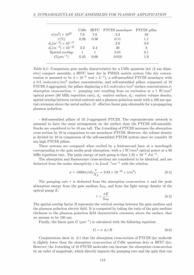
6. SUPRAMOLECULAR SELF-ASSEMBLIES FOR PLASMON AMPLIFICATION
CdSe HITC PTCDI monolayer PTCDI pillarσ(m2)× 1020 7.6 7.6 3.3 33
τ(%) 0.26 0.36 0.11 1.1ds(m
−2)× 10−17 3.0 3.0dv(m
−3)× 10−25 2.2 2.4 30 3Spatial overlap 1 1 0.01 0.1
G(µm−1) 0.45 0.66 0.019 1.9
Table 6.1: Comparison gain media characteristics for a CdSe quantum dot (2 nm diam-eter) compact assembly, a HITC laser dye in PMMA matrix system (the dye concen-tration is assumed to be 4 × 10⁻² mol × L−1), a self-assembled PTCDI monolayer witha 0.5 molecules/nm2 surface concentration, and self-assembled pillars composed of 10PTCDI J-aggregated, the pillars displaying a 0.5 molecules/nm2 surface concentration.σ:absorption cross-section, τ : pumping rate resulting from an excitation at a 1 W/mm2
optical power (80 MHz repetition rate), ds: emitter surface, dv: emitter volume density,spatial overlap between excited emitters and a plasmon polariton mode with a 100 nm spa-tial extension above the metal surface, G: effective linear gain obtainable for a propagatingplasmon polariton.
- Self-assembled pillars of 10 J-aggregated PTCDI. The supramolecular network isassumed to have the same arrangement on the surface than the PTCDI self-assembly.Stacks are considered to be 10 nm tall. The J-stacking of PTCDI increases the absorptioncross section by 10 in comparison to one monolayer PTCDI. However, the volume densityis divided by 10 in comparison of the self-assembled PTCDI system since we consider 10nm high PTCDI pillars.
These systems are compared when excited by a femtosecond laser at a wavelengthcorresponding to the gain media peak absorption, with a 1 W/mm2 optical power at a 80MHz repetition rate. The pulse energy of such pump is then 1.25× 10⁻² Jm−2.
The absorption and fluorescence cross-sections are considered to be identical, and arededucted from the molar absorptivity ǫ in Lmol−1cm−1 with the relation:
σ = 1000ln(10)ǫ
NA= 3.82× 10⁻²¹ ǫ (cm2) (6.4)
The pumping rate τ is deducted from the absorption cross-section σ and the peakabsorption energy from the gain medium hω0, and from the light energy density of theoptical pump E:
τ =σE
hω0(6.5)
The spatial overlap factor R represents the vertical overlap between the gain medium andthe plasmon polariton electric field. It is computed by taking the ratio of the gain mediumthickness to the plasmon polariton field characteristic extension above the surface, thatwe assume to be 100 nm.
Finally, the linear gain G (µm−1) is calculated with the following equation:
G = σ dvτR (6.6)
Computations show in 6.1 that the absorption cross-section of PTCDI dye moleculeis slightly lower than the absorption cross-section of CdSe quantum dots or HITC dye.However, the J-stacking of 10 PTCDI molecules can increase the absorption cross-sectionby an order of magnitude, which directly impacts the pumping rate and the gain that can
112
6. SUPRAMOLECULAR SELF-ASSEMBLIES FOR PLASMON AMPLIFICATION
be obtained. The volume density of the self-assembled PTCDI monolayer is much largerthan for the other compared systems. When J-aggregated, the PTCDI volume density losesan order of magnitude since one should consider J-aggregates and not PTCDI moleculesalone anymore.
As displayed in the table 6.1, the gain that can be obtained from a molecular self-assembly monolayer is two orders of magnitudes below what can be obtained with volumegain media. These two orders of magnitude are directly linked with the fact the monolayercovers only 1% of the plasmon polariton field. The number of dye molecules that interactwith the plasmon mode has to be increased in order to compete with traditional gainmedia.
Surprisingly, one should note that self-assembling 10 J-stacked PTCDI is sufficient tosurpass the characteristics of traditional gain media by a factor of 3, and by an order ofmagnitude if 20 PTCDI are J-stacked. The full losses compensation for a gold plasmonicwaveguide requiring a 2 µm−1 gain173 will then be achievable at low pumping power(1.1 W/mm2 at a 80 MHz repetition rate). The advantages of the J-stacked PTCDIsystem mainly result from the aggregation of the molecule which on the one hand allowsto obtain many molecules interacting with the plasmon mode and, on the other hand, ahigh pumping rate at a given excitation power resulting from the collective behavior ofthe system. Furthermore, the J-aggregation can induce a concentration of the oscillatorstrength in the fluorescence spectrum that directly leads to an increase of the fluorescencecross-section and thus to an enhancement of the linear gain.
Molecular self-assemblies appear as an alternative for gain media currently used inthe amplification of confined electromagnetic modes. These systems would be particularlysuitable for the stimulated emission of plasmons thanks to high surface densities that canbe obtained and to the possibility of creating J-aggregates that enhance assembled dyephotonic properties. More specifically, the self-assembly of pillars formed by J-aggregationof dye molecules could be of great use for the development of plasmonic based amplifiersand lasers, and more generally for the amplification of confined electromagnetic modes.
6.2 Gain limitations in self-assembled thin films
Solid state organic gain media have been studied for a long time since they benefit fromthe advantages of organic material such as tunable, compact and low-cost sources whileavoiding the inconvenient use of toxic solvents used in liquid dye lasers.174 Moreover,the use of a solid state may improve the dye photostability by preventing the diffusionof oxygen and moisture175 and decrease the lasing threshold by massively increasing thenumber of emitters interacting with the cavity electromagnetic mode,157,176 which aretwo major limitation to the development of organic laser systems. However, photonicsproperties of dye molecules are usually radically different between the solid and the liquidphase since intermolecular interactions lead to fluorescence quenching177 and absorptionand fluorescence spectra redistribution over visible frequencies.
Reducing the intermolecular interactions such as π-stacking can be done by design-ing molecular geometries that isolate the emissive part from neighbors thanks to highlybranched groups.178 However, the introduction of these spacer groups increases the amor-phous character of the thin film and decrease its molecular packing density. In the contextof surface plasmon polariton amplification, the organization of the film plays an impor-tant role since the propagating mode electromagnetic field is mostly normal to the metalsurface. Therefore, an anisotropic gain medium is needed to optimize the coupling fromemitters to the plasmon polariton mode.
Perylene derivative 2,9-Diheptylanthra [2,1,9-def : 6,5,10-d’e’f’] diisoquinoline-1,3,8,10(2H,9H) tetrone (PTCDI-C7) thin film grew by molecular beam epitaxy presents both
113

6. SUPRAMOLECULAR SELF-ASSEMBLIES FOR PLASMON AMPLIFICATION
Figure 6.3: Left. Fluorescent spectra of a 30 nm PTCDI-C7 thin film on gold for increasingpumping power at 460 nm from 20 µW to 4 mW with reference to the same gold substratewithout any molecules. The spectra have been normalized on the intensity of the 680 nmband. Right. Fluorescence decays at various pumping power.
an organization with the molecular main axis nearly normal to the substrate surface (seeChapter 1) and a relatively good fluorescence quantum efficiency (QE ∼ 10%) (see Chapter2). It may thus be a good candidate to be used as a solid-state gain medium for plasmonpolariton amplification. However, the compensation of the plasmonic losses requires highgain coefficients only achievable with large excitation ratios.
In the following, photodynamic properties of a 30 nm thick PTCDI-C7 thin film arestudied to explore which physical phenomena limit its use as gain medium, such as excitonrecombination at such high pumping rates.
6.2.1 Yield, spectrum and decay dependence on pump power
A 30 nm thick self-assembled PTCDI-C7 layer on top of various substrates (gold, SiO2 andITO on SiO2) was excited at a 460 nm wavelength by a doubled Ti:Sapphire femtosecondlaser focused onto the sample through a microscope objective (NA=0.6, x40). Fluorescencespectra were collected from a microscope immersion objective (NA=1.3, x100) on the otherside of the sample. Figure 6.3 displays normalized fluorescence spectra for the PTCDI-C7on gold hybrid system for pumping power ranging from 20 µW to 4 mW . Two clear bandsare visible on the spectra at 620 nm and 680 nm and a shoulder can be distinguished at720 nm. Surprisingly, the oscillator strength is redistributed from the 680 nm to the 620nm band when increasing the pump power. A consequent reduction of the fluorescencelifetimes accompany this fluorescence spectrum redistribution, as shown in figure 6.3. At20 µW pumping power, the fluorescence lifetime is estimated to 1.1 ns and decreases below0,1 ns (setup detection limit) at 200 µW pumping power.
Figure 6.4 shows the variations of the two fluorescence bands intensities with referenceto the pumping power in a logarithmic scale for the three different substrates. First,the PTCDI-C7 thin film on SiO2 fluorescence intensity at low pumping power is oneorder of magnitude larger than on ITO on SiO2 and two orders of magnitude larger thanon gold. The coupling of emitters to dark modes of ITO and gold through a Forstermechanism can be invoked to explain such difference. Furthermore, the different nature ofthe three substrates could lead to small differences in the dye orientation with respect tothe substrate during the assembly process and could then result in enhancing or decreasing
114
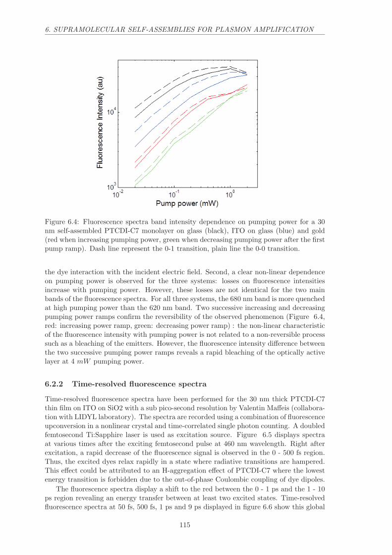
6. SUPRAMOLECULAR SELF-ASSEMBLIES FOR PLASMON AMPLIFICATION
Figure 6.4: Fluorescence spectra band intensity dependence on pumping power for a 30nm self-assembled PTCDI-C7 monolayer on glass (black), ITO on glass (blue) and gold(red when increasing pumping power, green when decreasing pumping power after the firstpump ramp). Dash line represent the 0-1 transition, plain line the 0-0 transition.
the dye interaction with the incident electric field. Second, a clear non-linear dependenceon pumping power is observed for the three systems: losses on fluorescence intensitiesincrease with pumping power. However, these losses are not identical for the two mainbands of the fluorescence spectra. For all three systems, the 680 nm band is more quenchedat high pumping power than the 620 nm band. Two successive increasing and decreasingpumping power ramps confirm the reversibility of the observed phenomenon (Figure 6.4,red: increasing power ramp, green: decreasing power ramp) : the non-linear characteristicof the fluorescence intensity with pumping power is not related to a non-reversible processsuch as a bleaching of the emitters. However, the fluorescence intensity difference betweenthe two successive pumping power ramps reveals a rapid bleaching of the optically activelayer at 4 mW pumping power.
6.2.2 Time-resolved fluorescence spectra
Time-resolved fluorescence spectra have been performed for the 30 nm thick PTCDI-C7thin film on ITO on SiO2 with a sub pico-second resolution by Valentin Maffeis (collabora-tion with LIDYL laboratory). The spectra are recorded using a combination of fluorescenceupconversion in a nonlinear crystal and time-correlated single photon counting. A doubledfemtosecond Ti:Sapphire laser is used as excitation source. Figure 6.5 displays spectraat various times after the exciting femtosecond pulse at 460 nm wavelength. Right afterexcitation, a rapid decrease of the fluorescence signal is observed in the 0 - 500 fs region.Thus, the excited dyes relax rapidly in a state where radiative transitions are hampered.This effect could be attributed to an H-aggregation effect of PTCDI-C7 where the lowestenergy transition is forbidden due to the out-of-phase Coulombic coupling of dye dipoles.
The fluorescence spectra display a shift to the red between the 0 - 1 ps and the 1 - 10ps region revealing an energy transfer between at least two excited states. Time-resolvedfluorescence spectra at 50 fs, 500 fs, 1 ps and 9 ps displayed in figure 6.6 show this global
115
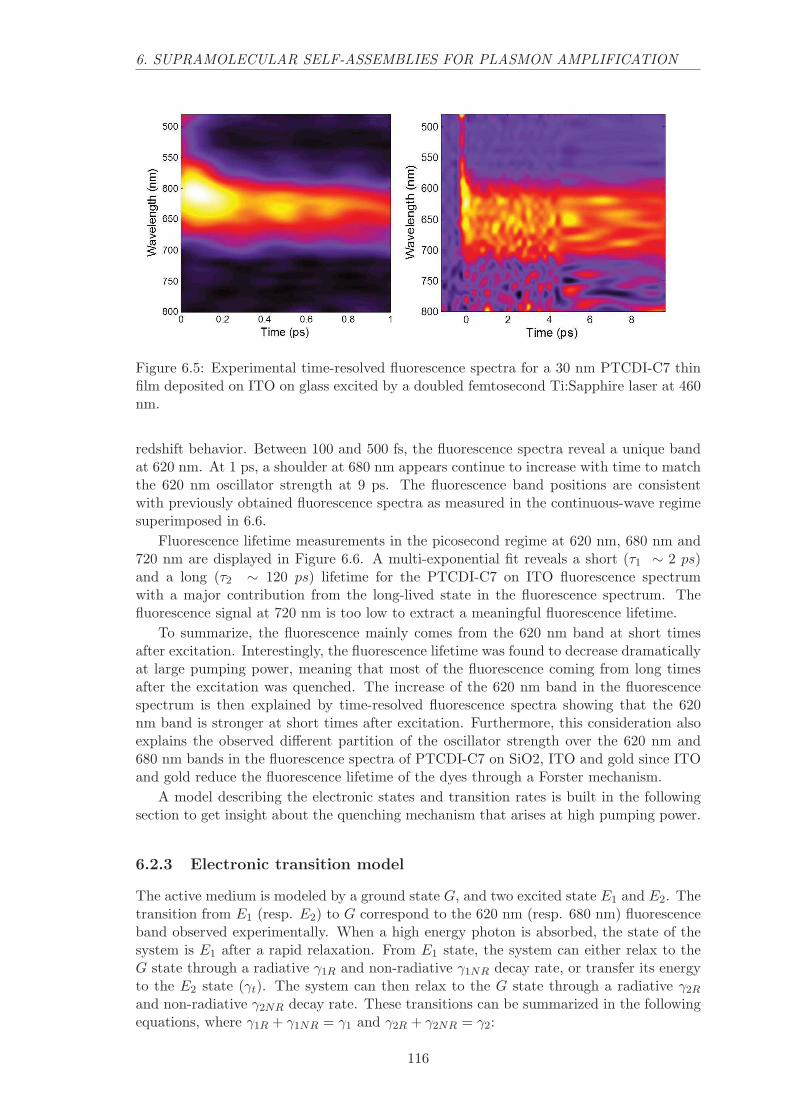
6. SUPRAMOLECULAR SELF-ASSEMBLIES FOR PLASMON AMPLIFICATION
Figure 6.5: Experimental time-resolved fluorescence spectra for a 30 nm PTCDI-C7 thinfilm deposited on ITO on glass excited by a doubled femtosecond Ti:Sapphire laser at 460nm.
redshift behavior. Between 100 and 500 fs, the fluorescence spectra reveal a unique bandat 620 nm. At 1 ps, a shoulder at 680 nm appears continue to increase with time to matchthe 620 nm oscillator strength at 9 ps. The fluorescence band positions are consistentwith previously obtained fluorescence spectra as measured in the continuous-wave regimesuperimposed in 6.6.
Fluorescence lifetime measurements in the picosecond regime at 620 nm, 680 nm and720 nm are displayed in Figure 6.6. A multi-exponential fit reveals a short (τ1 ∼ 2 ps)and a long (τ2 ∼ 120 ps) lifetime for the PTCDI-C7 on ITO fluorescence spectrumwith a major contribution from the long-lived state in the fluorescence spectrum. Thefluorescence signal at 720 nm is too low to extract a meaningful fluorescence lifetime.
To summarize, the fluorescence mainly comes from the 620 nm band at short timesafter excitation. Interestingly, the fluorescence lifetime was found to decrease dramaticallyat large pumping power, meaning that most of the fluorescence coming from long timesafter the excitation was quenched. The increase of the 620 nm band in the fluorescencespectrum is then explained by time-resolved fluorescence spectra showing that the 620nm band is stronger at short times after excitation. Furthermore, this consideration alsoexplains the observed different partition of the oscillator strength over the 620 nm and680 nm bands in the fluorescence spectra of PTCDI-C7 on SiO2, ITO and gold since ITOand gold reduce the fluorescence lifetime of the dyes through a Forster mechanism.
A model describing the electronic states and transition rates is built in the followingsection to get insight about the quenching mechanism that arises at high pumping power.
6.2.3 Electronic transition model
The active medium is modeled by a ground state G, and two excited state E1 and E2. Thetransition from E1 (resp. E2) to G correspond to the 620 nm (resp. 680 nm) fluorescenceband observed experimentally. When a high energy photon is absorbed, the state of thesystem is E1 after a rapid relaxation. From E1 state, the system can either relax to theG state through a radiative γ1R and non-radiative γ1NR decay rate, or transfer its energyto the E2 state (γt). The system can then relax to the G state through a radiative γ2Rand non-radiative γ2NR decay rate. These transitions can be summarized in the followingequations, where γ1R + γ1NR = γ1 and γ2R + γ2NR = γ2:
116
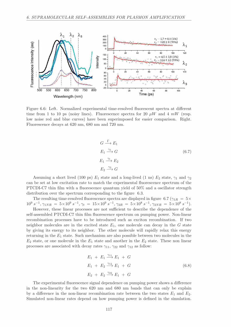
6. SUPRAMOLECULAR SELF-ASSEMBLIES FOR PLASMON AMPLIFICATION
Figure 6.6: Left. Normalized experimental time-resolved fluorescent spectra at differenttime from 1 to 10 ps (noisy lines). Fluorescence spectra for 20 µW and 4 mW (resp.low noise red and blue curves) have been superimposed for easier comparison. Right.Fluorescence decays at 620 nm, 680 nm and 720 nm.
GΓ−→ E1
E1γ1−→ G (6.7)
E1γt−→ E2
E2γ2−→ G
Assuming a short lived (100 ps) E1 state and a long-lived (1 ns) E2 state, γ1 and γ2can be set at low excitation rate to match the experimental fluorescence spectrum of thePTCDI-C7 thin film with a fluorescence quantum yield of 50% and a oscillator strengthdistribution over the spectrum corresponding to the figure 6.3.
The resulting time-resolved fluorescence spectra are displayed in figure 6.7 (γ1R = 5×10⁹ s−1, γ1NR = 5×10⁹ s−1, γt = 15×109 s−1, γ2R = 5×10⁸ s−1, γ2NR = 5×10⁸ s−1).
However, these linear processes are not sufficient to describe the dependence of theself-assembled PTCDI-C7 thin film fluorescence spectrum on pumping power. Non-linearrecombination processes have to be introduced such as exciton recombination. If twoneighbor molecules are in the excited state E1, one molecule can decay in the G stateby giving its energy to its neighbor. The other molecule will rapidly relax this energyreturning in the E1 state. Such mechanism are also possible between two molecules in theE2 state, or one molecule in the E1 state and another in the E2 state. These non linearprocesses are associated with decay rates γ11, γ22 and γ12 as follow:
E1 + E1γ11−→ E1 + G
E1 + E2γ12−→ E1 + G (6.8)
E2 + E2γ22−→ E1 + G
The experimental fluorescence signal dependence on pumping power shows a differencein the non-linearity for the two 620 nm and 680 nm bands that can only be explainby a difference in the non-linear recombination rate between the two states E1 and E2.Simulated non-linear rates depend on how pumping power is defined in the simulation.
117

6. SUPRAMOLECULAR SELF-ASSEMBLIES FOR PLASMON AMPLIFICATION
Figure 6.7: Left. Computer simulated time-resolved fluorescence intensity of the 620 nmband (red), the 680 nm band (blue) and the sum of these two bands (black). Computersimulated time resolved fluorescence spectra between times t1 and t2.
Figure 6.8: Computed fluorescence spectra band intensity dependance on pumping power.The red (resp. blue) line represent the 0-0 (resp. 0-1) transition.
118

6. SUPRAMOLECULAR SELF-ASSEMBLIES FOR PLASMON AMPLIFICATION
We retrieve the experimental behavior for the fluorescence spectrum when setting γ11 =1011 s−1, γ12 = 6× 10⁹ s−1 and γ22 = 6× 10⁹ s−1, as displayed in figure 6.8.
The model can be summarized with the following set of equations describing the tem-poral evolution of the population NG, N1 and N2 of the respective states G, E1 andE2:
dNG
dt= (−Γ + γ1)N1 + γ2N2 + γ11N
21 + γ22N
22 + γ12N1N2 (6.9)
dN1
dt= (Γ− γ1)NG − γtN2 − γ11N
21 + γ12N1N2 (6.10)
dN2
dt= −γ2NG + γtN1 − γ22N
22 − γ12N1N2 (6.11)
The time-resolved fluorescence intensity at the instant t of the two bands then corre-sponds respectively to γ1RN1(t) and γ12N2(t). The pumping power is adjusted with theparameter N1(0), the population of the state E1 just after the excitation by the incidentlaser beam. The two transitions are considered to be lorentzian using a width that fitsthe experimental spectra at low pumping power.
6.3 Conclusion
Supramolecular self-assemblies open the perspective to obtain highly efficient gain mediathanks to a high concentration of dyes in the medium and the possibility to saturatethe active medium at low excitation rate when molecules behave collectively forming J-aggregates. These system have the potential to surpass the gain of active media such asdyes in a polymer matrix or assemblies of quantum dots by at least one order of magnitude.
Self-assembled PTCDI-C7 thin films on top of various substrates have been opticallycharacterized to probe their photonic properties as potential gain media for amplifyingsurface plasmon polaritons. Linear and non-linear non radiative recombination processesreduce the fluorescence quantum yield due to intermolecular interactions such as exciton-exciton recombination and therefore limit the performances of this active media, especiallyat high excitation rates. The fluorescence quantum yield estimated at 10% at low pumpingrates decreases to 1% at high pumping rates. A careful design of the assembling build-ing block should be undertaken to reduce these limiting effects by, for example, spacingthe dyes while maintaining sufficient intermolecular interactions to form a self-assembledsystem.
119

6. SUPRAMOLECULAR SELF-ASSEMBLIES FOR PLASMON AMPLIFICATION
120
Summary
As a bottom-up approach, supramolecular self-assembly allows the design of matter at thenanometer scale through the control of intermolecular distances and orientations. In thiswork, we have studied optical absorption, fluorescence and vibrational properties of two-and three-dimensional dye self-assemblies exploring how these photonic characteristicsdepend on intermolecular and molecule-substrate interactions.
In chapter 1, we have studied several dye self-assemblies on graphene forming well-defined two-dimensional networks with geometrical parameters characterized by STM ex-periments. Transmission absorption measurements have shown a rigid redshift of the ab-sorption spectra in comparison to the same dyes dispersed in a toluene solution with minormodifications in the peak structure of the absorption spectra. We were able to observe asignificant change in the oscillator strength distribution over the S0-S1 vibronic replicasby varying the intermolecular distances in self-assembled perylene derivative monolayerson graphene. We have attributed this effect to Coulombic dipole-dipole couplings be-tween neighbor molecules. Self-assembled molecules with a dye group standing away fromthe graphene surface have displayed a smaller redshift of their optical absorption peak.Therefore, the modification of the dielectric environment due to the high refractive indexof graphene and the spatial overlap between the sp2 orbitals of graphene and the adsorbeddye have appeared to be the main phenomena altering the dye absorption spectrum onceself-assembled on the graphene surface. We have demonstrated the possibility to extendthese two-dimensional self-assemblies to three dimensions by evaporating perylene-dyederivatives at a slow deposition rate on heated surfaces.
Adsorbed dyes on graphene lose their fluorescence due to both Dexter and Forstertype energy transfers toward non-radiative excited states. Nevertheless, we have shownin chapter 2 that a fluorescent molecular self-assembled monolayer on graphene has beenobtained with the use of a 3D Janus tecton embedding a PTCDI dye spaced from apedestal group steering the assembly at the graphene surface. We have demonstrated thefirst fluorescent functionalization of graphene with a self-assembled molecular monolayer.A multilayer self-assembled system with a 10% fluorescence quantum efficiency has beendemonstrated, paving the way to self-assembled optical gain media.
The fluorescence quenching of self-assembled dyes by graphene has been exploited inchapter 3 to measure vibrational properties of self-assembled molecules by Raman spec-troscopy. This have provided the opportunity to measure for the first time the Ramanresponse of PTCDI, which is normally made impossible by its fluorescence both in solu-tion and in solid state. A low frequency graphene-molecule coupled mode called ”Mambomode” has been demonstrated to appear in the Raman spectra of self-assembled moleculeson graphene.
In chapter 4, we have described useful theoretical and experimental tools to predictand characterize plasmonic modes. We have experimentally determined the dispersionrelation of a surface plasmon polariton propagating at the surface of a 40 nm thick goldwaveguide. We have shown that the approach of Coulombic coupling between neighborplasmon modes could enhance the quality factor of plasmonic modes.
Strong-coupling between a 30 nm thick self-assembled PTCDI-C7 layer and surface
121

SUMMARY
plasmon polaritons propagating on a gold layer has been demonstrated in chapter 5. A 110meV anti-crossing around the 560 nm absorption peak of PTCDI-C7 has been measured.Matrix-transfer computations have retrieved the absorption and emission response of thehybrid system. This strong-coupling regime has resulted from the high emitter densityof the self-assembled gain medium and the orientation of the molecules inside the gainlayer with respect to the electric field of the plasmon mode that have optimized theinteraction between the gain medium and the surface plasmon mode. Since the self-assembled PTCDI-C7 have shown an important Stokes shift, absorption and fluorescencespectra did not overlap and no anti-crossing has been observed in emission. Matrix-transfersimulations have shown that this behavior is consistent with the picture of dyes drivingthe electromagnetic field.
Theoretical considerations have shown that dye self-assemblies could surpass tradi-tional optical gain media by one order of magnitude. However, we have demonstrated inchapter 6 that intermolecular interactions such as exciton-exciton recombination have low-ered consequently the fluorescence quantum efficiency of the 30 nm thick self-assembledPTCDI-C7 layer. Molecular building blocks should therefore be carefully designed tominimize such limiting interactions while keeping their self-assembling nature.
122

Synthese
La miniaturisation des technologies optiques se heurte a la limite physique du confine-ment du champ electromagnetique a des echelles inferieures a la longueur d’onde. Cettelimite pourrait etre repoussee en etendant aux echelles optiques les antennes et guidesmetalliques utilises pour les ondes Hertziennes. Ce nouveau domaine de l’optique, appeleplasmonique, ouvre la perspective du developpement de nano-lasers par association d’unmilieu optiquement actif a un resonateur plasmonique.
Toutefois, la distribution spatiale du champ electrique tres specifique des modes plas-moniques impose de nouvelles contraintes sur les milieux a gain. Les milieux optiquementactifs classiques doivent etre repenses pour permettre le developpement de nano-dispositifsoptiques efficaces.
Dans cette these, nous explorons les possibilites d’utiliser les auto-assemblages supra-moleculaires, dont les proprietes photoniques sont peu connues, comme milieux optique-ment actifs de nouvelle generation pour les technologies optiques a l’echelle sub-longueurd’onde.
Au chapitre 1, nous etudions l’absorption optique de monocouches de derives deperylene auto-assembles a la surface du graphene. Nous montrons que les proprietes op-tiques des auto-assemblages de colorants a deux dimensions sur le graphene dependent desinteractions intermoleculaires et des interactions colorant-graphene, et peuvent etre varieesen changeant la geometrie de l’assemblage du colorant sur le graphene. Nous montronscomment obtenir un auto-assemblage tridimensionnel de derives de perylene optimisantune interaction possible avec un plasmon polariton de surface.
Le deuxieme chapitre traite de la fluorescence de couches auto-assemblees sur graphene.La premiere fonctionnalisation fluorescente non covalente du graphene par une mono-couche auto-assemblee de colorant est demontree, grace a l’utilisation de tectons Janus.La fluorescence des auto-assemblages tridimensionnels optimises pour l’interaction avecdes plasmons polaritons de surface est etudiee.
Dans le troisieme chapitre, nous explorons les proprietes vibrationnelles des mono-couches auto-assemblees sur le graphene par des calculs de theorie de la fonctionnelle de ladensite et des experiences de spectroscopie Raman. Nous montrons l’apparition d’un modevibrationnel couple entre les molecules adsorbes sur le graphene et le graphene lui-meme,que nous nommons le mode ”Mambo”.
Le chapitre quatre presente les techniques theoriques (simulation par transfert de ma-trice, constante dielectrique de materiaux hybrides) et experimentales permettant de car-acteriser les plasmons polaritons de surface dans le but de reduire les pertes des resonateursplasmoniques. Nous proposons une strategie lors du design du resonateur pour optimiserle facteur de qualite de la resonance.
Nous demontrons dans le chapitre cinq un regime de couplage fort entre des plasmonspolaritons de surface et un auto-assemblage tridimensionnel de colorant ayant un impor-tant deplacement de Stokes. Les proprietes photoniques du systeme couple sont etudieesexperimentalement et theoriquement par sa reponse en absorption et en emission, notam-ment pour explorer les liens entre anti-croisements et deplacement de Stokes.
Enfin, le chapitre six presente les conditions theoriques permettant d’amplifier des
123

SYNTHESE
plasmons polaritons de surface, et compare les performances de gain atteignable par lessystemes auto-assembles aux milieux a gain traditionnels. Les limitations sur le gaindes couches auto-assemblees sont etudiees experimentalement par des spectres de fluo-rescence resolus dans le temps ainsi que par la dependance du spectre de fluorescenceavec la puissance de pompage du milieu. D’importantes pertes liees aux recombinaisonsexciton-exciton sont caracterisees a fort taux de pompage, limitant l’efficacite de ce nou-veau milieu a gain. Un modele prenant en compte les effets lineaires et non-lineairespermettant d’expliquer la dynamique de fluorescence ainsi que le comportement du signalde fluorescence avec la puissance de pompe est propose.
124

Appendix A
Dipole-field interactions
theoretical calculations
A.1 Frequency to local electric field shifts relation demon-
stration
In a 1D framework, we model the molecule by a moving electron cloud and a static positivecharge cloud. The electron cloud is defined by a homogeneous linear partition of a chargedensity ρcand a mass density ρm with spatial extension L. The global neutrality of themolecule requires same characteristics for the positive charges cloud. (see figure A.1)
We consider that the displacement of the electron cloud is small in comparison to L.Local charges appear only at the extremity of the molecule, meaning this model leads toa condensator geometry where the electric field between the two charges Ein is constant.
We apply Newton’s law on a slice δx of negative charges:
ρmδxd2x
dt2= −ρcδxEin
Since the barycenter of positive charges does not move, we find the differential equationfor the dipole moment µ:
µ = ρcxL
d2µ
dt2= −ρ2cL
ρmEin
The condensator approximation allow to write the electric field Ein in terms of dipolemoment and others constants:
Ein =σ
ǫ0ǫr=
ρcx
ǫ0ǫrS=
µ
ǫ0ǫrV
Where σ is the surface charge density at the extremity of the molecule, and V = SL thespecific volume of charges at the extremity of the molecule. In the following, we note:β = ǫ0ǫrV .
Figure A.1: 1D molecule model
125
A. DIPOLE-FIELD INTERACTIONS THEORETICAL CALCULATIONS
The differential equation on the dipole moment can then be rewritten:
d2µ
dt2= − ρ2cL
ρmβµ
Without any perturbation from the environment such as an incident electromagneticwave or a retroaction of the environment through charge coupling, the electron cloud of
the molecule is an harmonic oscillator with frequency ω0 =√
ρ2cLρmβ
The differential equation on the dipole moment is modified with an incident electricfieldE0cos(ωt) as the following:
d2µ
dt2= −ρ2cL
ρm(µ
β+ E0cos(ωt))
We retrieve the usual lorentzian function for the dipole moment dependence on fre-quency:
µ(t) = µ0(ω)cos(ωt)
µ0(ω) =ρ2cL
ρm(ω2 − ω20
E0
If the environment produce a retroaction on the molecule creating the perturbativeelectric field Ep = kEin (where k can be complex to account for various delays in theretroaction), the harmonic oscillator have a shifted resonance frequency:
ω2p = (1 + k)ω2
0
The total electric field inside the molecule is in this case Ep = Ein+kEin. The shiftedresonance frequency ωp can thus be related to the resonance frequency and the electricfield for the lone molecule case as follow:
ωp
ω0=
√
Ep
Ein
126

A. DIPOLE-FIELD INTERACTIONS THEORETICAL CALCULATIONS
Figure A.2: Incident, reflected and transmitted electromagnetic fields on a molecularmonolayer in a transverse electric configuration (TE).
A.2 Absorption of an oriented dipole monolayer
In this part, the reflection and transmission coefficients of a electromagnetic wave inci-dent on a molecular monolayer are computed. Scheme A.2 describes the problem of theabsorption of light by a molecular monolayer represented by polarizability α.
An incident electromagnetic (Ei,Hi,ki) field is directed onto the monolayer interfacewhich transmits the field (Et,Ht,kt) and reflects the field (Er,Hr,kr).
A.2.1 Transverse electric polarization
The Maxwell-Faraday equation makes a link between the electric and the magnetic field:
∇×E = − ∂
∂tB
The electric field circulation on a path around the surface is null when the thickness t ofthe monolayer tends to 0.
limt→0
∫
0Edl = 0
The contribution of the paths parallel to the surface is:
∫
‖Edl = E1∂y − E2∂y
The contribution of the paths perpendicular to the surface is null since µ⊥ = 0. Theequation on the electric field circulation then gives:
E1 = E2
127
A. DIPOLE-FIELD INTERACTIONS THEORETICAL CALCULATIONS
The Maxwell-Ampere equation links the magnetic field to the electric displacementand the surface current:
∇×H = j+∂
∂tD
A surface current exists in the molecular monolayer:
j =∂
∂tµ = −iωµ
Therefore, the circulation of magnetic field can be written:∫
‖Hdl = H1∂y −H2∂y = −iωµ‖∂x
H2‖ −H1‖ = iωµ‖
Field continuity relationship can thus be written as:
Ei + Er = Et
Hicos(θ1)−Hrcos(θ1) = Htcos(θ2)− iωµ‖
For a plane wave propagating in the dielectric environment with refractive index n, themagnetic field continuity equation can be rewritten as:
Ein1cos(θ1)− Ern1cos(θ1) = Etn2cos(θ2)− iωα‖
ǫ0cEt
Since the dipole moment is linked to the electric field by mu‖ = α‖Et.The extended Fresnel coefficient is then:
Et
Ei=
2n1cos(θ1)
n2cos(θ2) + n1cos(θ1)− iωα‖
ǫ0c
A.2.2 Transverse magnetic polarization
Scheme A.3 represents electromagnetic fields in the transverse magnetic (TM) polariza-tion.
The electric field circulation by a parallel path to the surface can be written:∫
‖Edl = E1‖∂x− E2‖∂x
The circulation by a perpendicular path is more complex. The interface thickness t isdefined as the separation distance between two charged planes that are equivalent to thesurface dipole distribution:
µ⊥ = σt
Between these two planes, the electric field can be written:
Eµ⊥=
σ
ǫ0=
µ⊥
2ǫ0t
The electric field circulation is then calculated when the thickness tends to zero:∫
0Edl =
∫
⊥Edl+
∫
‖Edl
limt→0
∫
⊥Edl =
µperp(x+ ∂x
ǫ0− µperp(x
ǫ0
128

A. DIPOLE-FIELD INTERACTIONS THEORETICAL CALCULATIONS
Figure A.3: Incident, reflected and transmitted electromagnetic fields on a molecularmonolayer in a transverse magnetic configuration (TM).
Which simplifies to:
E2‖ − E1‖ =1
ǫ0
∂µ⊥(x)
∂x
E2‖ − E1‖ =ikxµ⊥
ǫ0
Surface current j exists and in the context of propagating plane wave at pulsation ωand this surface current can be written:
j =∂
∂tµ = −iωµ
The circulation of magnetic field around the surface is then:
∫
0Hdl = H1∂y −H2∂y = −iωµ‖∂y
Continuity equations can be summarized:
E2‖ − E1‖ =ikxµ⊥
2ǫ0=
iωµ⊥
ǫ0cn2sin(θ2)
H2 −H1 = iωµ‖
Since the electric field continuity equation depends on the dipolar moment µ⊥, one hasto choose on which side of the interface the dipoles are located. If dipoles lay on thetransmitted side, the continuity equation on the electric field can be written:
Eicos(θ1)− Ercos(θ1) = Etcos(θ2)−iωα⊥
ǫ0cn2(sin(θ2))
2Et
129

A. DIPOLE-FIELD INTERACTIONS THEORETICAL CALCULATIONS
The resolution of the two equation system gives the extended Fresnel coefficient:
Et
Ei=
2 cos(θ1)n1
cos(θ1)n1
+ cos(θ2)n2
− iωǫ0cn2
(α⊥2 n2sin(θ2)2 +
α‖
n1cos(θ1)cos(θ2))
In the case of dipoles laying on the incident side of the surface, the electric fieldcontinuity equation and the Fresnel extended coefficient can be written:
Eicos(θ1)− Ercos(θ1) = Etcos(θ2)−iωα⊥
2ǫ0cn2sin(θ2)(Ei + Er)sin(θ1)
Et
Ei=
2 cos(θ1)n1
cos(θ1)n1
+ cos(θ2)n2
− iωǫ0cn1
(α⊥n2sin(θ1)sin(θ2)−α‖
n2cos(θ1)cos(θ2)) +
ω2α⊥α‖
ǫ20c2n1
sin(θ2)sin(θ1)cos(θ2)
130

Appendix B
Self-assembled systems on
graphene absorption spectra
B.1 Table of experimental shifts and broadenings
Several supramolecular self-assemblies on graphene have been optically characterized bytransmission absorption measurements. The principal absorption peak position and peakwidth in solution and self-assembled on graphene are synthetized in figure B.1. All ofprincipal peaks are shifted to the red by a energy ranging from 50 to 500 meV whencomparing the absorption of the self-assembled system on graphene to the same moleculediluted in a solution. Alternatively, the width of the principal peak is either increased orreduced depending on the system. The change in peak width (FWHM) ranges from -100to 200 meV.
Figure B.1: Principal absorption peak position and width for various molecules diluted ina solution and self-assembled on graphene.
131

B. SELF-ASSEMBLED SYSTEMS ON GRAPHENE ABSORPTION SPECTRA
Figure B.2: Monomer molecular structure of polymers P3HT, P3DT and P3DDT. Trans-mission absorption spectra of P3HT (blue), P3DT (red) and P3DDT (green) diluted in atoluene solution (dark) and self-assembled on the graphene surface (light). The absorptionspectrum of a P3HT microcrystal on a SiO2 substrate is also displayed in grey.
B.2 Polymers on graphene
Absorption spectra of polythiophene polymers P3HT, P3DT and P3DDT and polythio-phene derivatives P3PT-Br, P3DT-Br and P3PDT-Br are displayed in figure B.2 andB.3. Once one the graphene surface, all polymer absorption spectra show an important∼ 500 meV redshift with reference to the absorption spectra taken with polymers dilutedin a toluene solution. It is worth to note that most of the redshift should not resultfrom interactions with the graphene surface since P3HT microcrystals on a glass substrateabsorption spectrum displays the same shift to lower frequencies. (see figure B.2).
However, a difference exists when comparing the shoulder at 625 nm. First, absorptionspectra of polymers on graphene display a 30 nm redshift with comparison to P3HTmicrocrystals. Second, the oscillator force of the 625 nm shoulder is decreased for polymerson graphene with reference to P3HT microcrystals. Interestingly, this shoulder is sensiblyreduced for P3PT-Br, P3DT-Br and P3PDT-Br with comparison to the main absorptionpeak once on the graphene surface.
Density functional theory calculations have been performed to predict the effect of thepolythiophene oligomer adsorption on a graphene surface on the polythiophene oligomerelectronic density of states (DOS). Calculated DOS for P3HT and P3DT oligomer (10monomers) in vacuum and adsorbed on a graphene surface are displayed in figure B.4.Calculated gaps for P3DT and P3HT oligomers are respectively 1.3 and 1.2 eV in vacuum.This result points out some imprecision with the calculation since absorption spectrain toluene solution show that the alkyl chain length do not interact with conjugatedthiophene rings since absorption spectra peak at the same frequency for P3HT and P3DT.Once adsorbed on the graphene surface, figure B.4 shows that the electronic DOS isimportantly modified. The calculation gives a 1.91 electron charge transfer from the P3HToligomer to the graphene, representing 0.32% of the total number of valence electrons. Asa result, for both calculated systems the whole DOS is shifted to higher energies. A 400meV and 200 meV reduction of the HOMO-LUMO gap for P3DT and P3HT oligomersrespectively accompanies the important modification of the DOS. The planarization of thepolythiophene oligomer increasing the electron conjugation length could explain this effect.Our deposition technique needs to be improved to assure the formation of a polythiophene
132
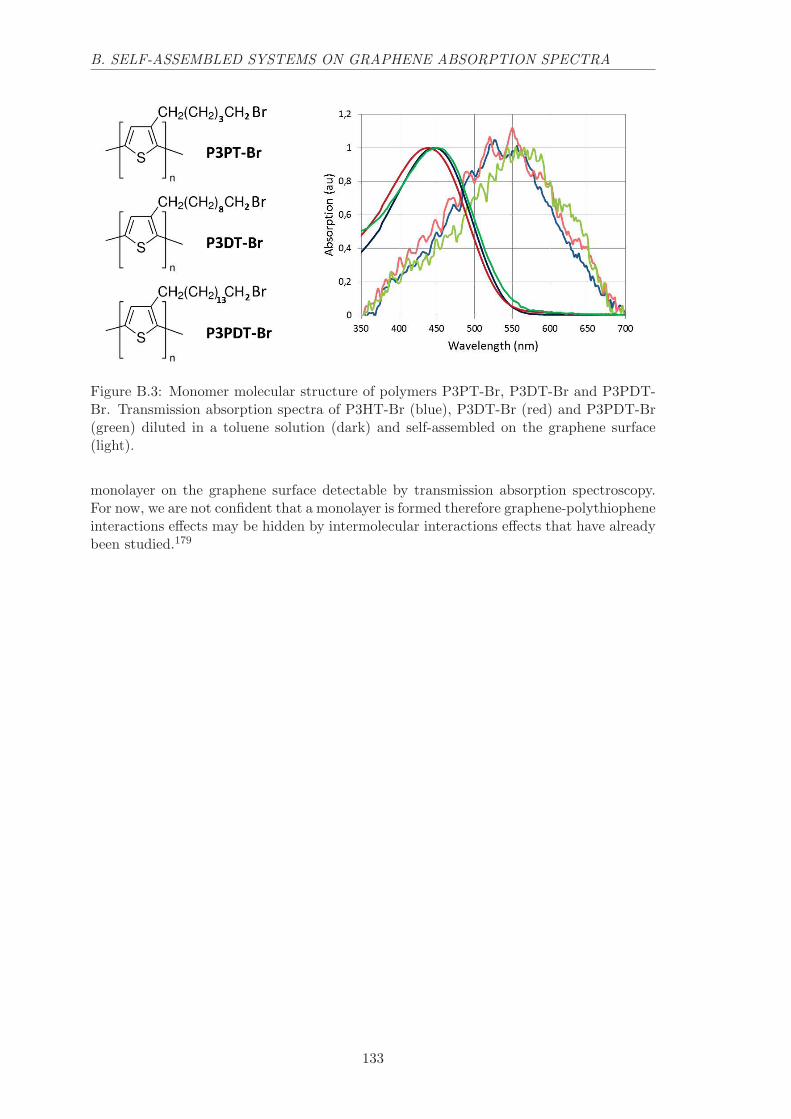
B. SELF-ASSEMBLED SYSTEMS ON GRAPHENE ABSORPTION SPECTRA
Figure B.3: Monomer molecular structure of polymers P3PT-Br, P3DT-Br and P3PDT-Br. Transmission absorption spectra of P3HT-Br (blue), P3DT-Br (red) and P3PDT-Br(green) diluted in a toluene solution (dark) and self-assembled on the graphene surface(light).
monolayer on the graphene surface detectable by transmission absorption spectroscopy.For now, we are not confident that a monolayer is formed therefore graphene-polythiopheneinteractions effects may be hidden by intermolecular interactions effects that have alreadybeen studied.179
133

B. SELF-ASSEMBLED SYSTEMS ON GRAPHENE ABSORPTION SPECTRA
Figure B.4: Electronic density of states (DOS) for P3DT (top) and P3DT (bottom)oligomers (10 monomers) in vacuum (black) and adsorbed on a graphene surface.
134

B. SELF-ASSEMBLED SYSTEMS ON GRAPHENE ABSORPTION SPECTRA
Figure B.5: Monomer molecular structure of PBDTTPD. Transmission absorption spectradiluted in a toluene solution (dark blue) and self-assembled on the graphene surface (lightblue).
The optical absorption of PBDTTPD thin layer on graphene and in solution are dis-played in figure B.5. The main absorption peak at 532 nm in solution is redshifted to584 nm once on graphene, corresponding to a 208 meV redshift. Interestingly, the well-resolved structure at 616 nm present in the solution absorption spectrum disappears whenthe polymer is deposited on graphene.
B.3 Small molecules on graphene
Figure B.6 displays the absorption spectrum of a squaraine dye (SQ−Bu2) drop casted ongraphene. A 130 meV redshift of the principal absorption peak is observed accompaniedby a 45 meV broadening of the peak. The idea is to find flat molecules to build multiplestacks of dye functionalized graphene. In a try to build such stacked system, it was notpossible to reproduce this absorption spectrum and we obtained a much larger absorptionpeak that might result from the presence of aggregated molecules instead of adsorbedmolecules on graphene.
Figure B.7 displays the absorption spectrum of a PTCDI derivative (PTCDI-d) ongraphene. PTCDI-d carries a large dendron at one extremity and alkyl chain at the otherextremity to try to lift the aromatic core from the graphene surface while retaining themolecule to the surface thanks to the alkyl chains present at the molecule extremity. Theabsorption spectrum is promising since the redshift of the 0-0 transition peak (528 nmin solution, 540 nm once on the graphene surface) is much lower than for other PTCDIderivatives such as PTCDI-C13, revealing lower interactions with the graphene surface (cf.Chapter 1). Further investigations should be done to precisely characterize the molecularself-assembly.
Figure B.8 displays the molecular structure and the absorption spectra of pCpT3in a toluene solution and self-assembled on the graphene surface. The dye group of themolecule is separated from the graphene surface by a self-assembling pedestal group (cfChapter 2) and a spacer group. This molecule has a very close structure from the TBC8-JT one. The same pedestal group is used, but the spacer group differs since a disulfurbridge is used in TBC8-JT. Finally, the pCpT3 dye group absorbs light in the 400 nmrange whereas TBC8-JT absorbs light in the 500 nm range. A 195 meV redshift of theprincipal absorption peak is observed between pCpT3 diluted in a toluene solution and
135

B. SELF-ASSEMBLED SYSTEMS ON GRAPHENE ABSORPTION SPECTRA
Figure B.6: Molecular structure of the squaraine dye SQ−Bu2. SQ−Bu2 transmissionabsorption spectrum diluted in a toluene solution (dark blue) and self-assembled on thegraphene surface (light blue).
Figure B.7: Molecular structure of the perylene derivative dye PTCDI-d. PTCDI-d trans-mission absorption spectrum on the graphene surface.
136

B. SELF-ASSEMBLED SYSTEMS ON GRAPHENE ABSORPTION SPECTRA
Figure B.8: Molecular structure of pCpT3. pCpT3 transmission absorption spectra dilutedin a toluene solution (dark blue) and self-assembled on the graphene surface (light blue).
self-assembled on the graphene surface. It is surprisingly close to the 192 meV redshiftobtained for the self-assembled TBC8-JT system.
137
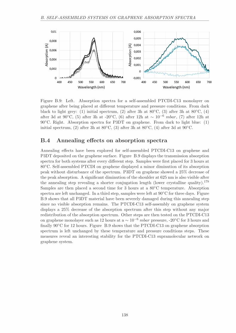
B. SELF-ASSEMBLED SYSTEMS ON GRAPHENE ABSORPTION SPECTRA
Figure B.9: Left. Absorption spectra for a self-assembled PTCDI-C13 monolayer ongraphene after being placed at different temperature and pressure conditions. From darkblack to light grey: (1) initial spectrum, (2) after 3h at 80◦C, (3) after 3h at 80◦C, (4)after 3d at 90◦C, (5) after 3h at -20◦C, (6) after 12h at ∼ 10−6 mbar, (7) after 12h at90◦C. Right. Absorption spectra for P3DT on graphene. From dark to light blue: (1)initial spectrum, (2) after 3h at 80◦C, (3) after 3h at 80◦C, (4) after 3d at 90◦C.
B.4 Annealing effects on absorption spectra
Annealing effects have been explored for self-assembled PTCDI-C13 on graphene andP3DT deposited on the graphene surface. Figure B.9 displays the transmission absorptionspectra for both systems after every different step. Samples were first placed for 3 hours at80◦C. Self-assembled PTCDI on graphene displayed a minor diminution of its absorptionpeak without disturbance of the spectrum. P3DT on graphene showed a 25% decrease ofthe peak absorption. A significant diminution of the shoulder at 625 nm is also visible afterthe annealing step revealing a shorter conjugation length (lower crystalline quality).179
Samples are then placed a second time for 3 hours at a 80◦C temperature. Absorptionspectra are left unchanged. In a third step, samples were left at 90◦C for three days. FigureB.9 shows that all P3DT material have been severely damaged during this annealing stepsince no visible absorption remains. The PTCDI-C13 self-assembly on graphene systemdisplays a 25% decrease of the absorption spectrum after this step without any majorredistribution of the absorption spectrum. Other steps are then tested on the PTCDI-C13on graphene monolayer such as 12 hours at a ∼ 10−6 mbar pressure, -20◦C for 3 hours andfinally 90◦C for 12 hours. Figure B.9 shows that the PTCDI-C13 on graphene absorptionspectrum is left unchanged by these temperature and pressure conditions steps. Thesemeasures reveal an interesting stability for the PTCDI-C13 supramolecular network ongraphene system.
138
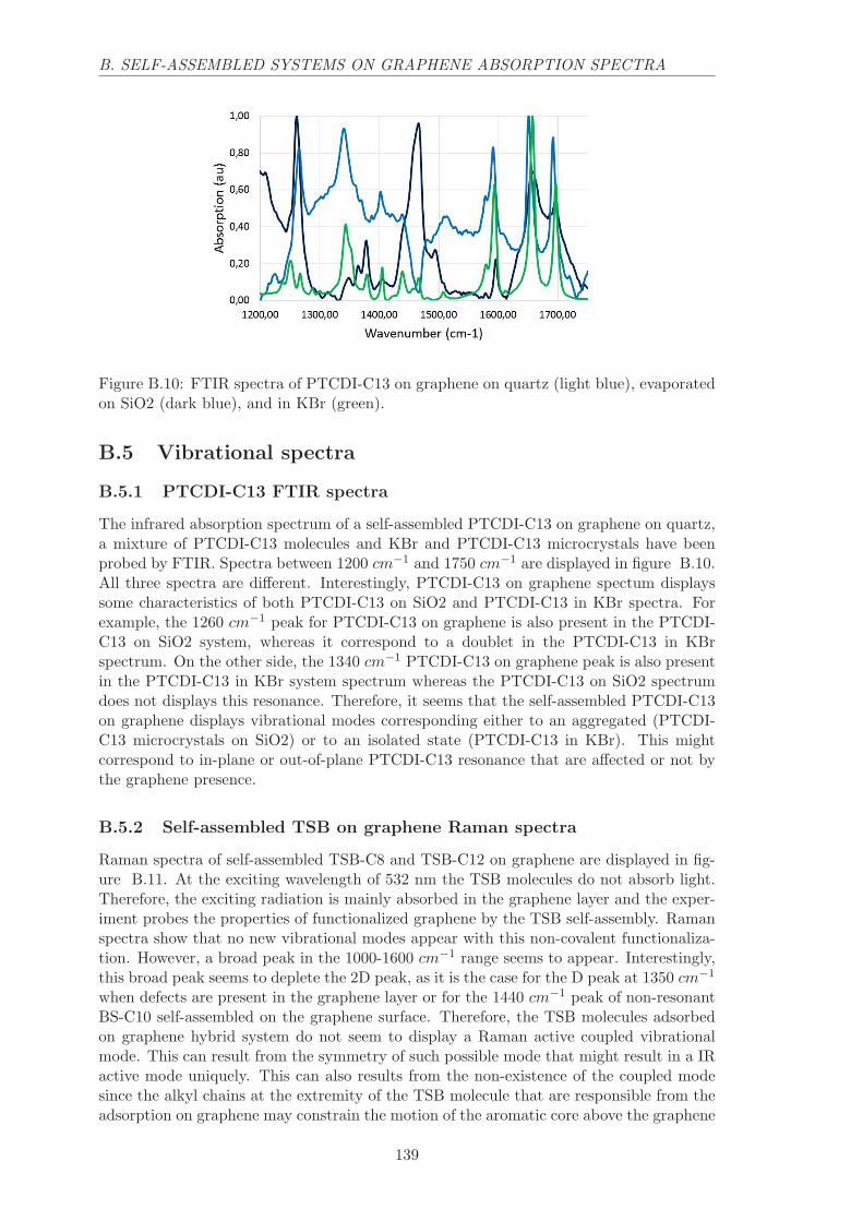
B. SELF-ASSEMBLED SYSTEMS ON GRAPHENE ABSORPTION SPECTRA
Figure B.10: FTIR spectra of PTCDI-C13 on graphene on quartz (light blue), evaporatedon SiO2 (dark blue), and in KBr (green).
B.5 Vibrational spectra
B.5.1 PTCDI-C13 FTIR spectra
The infrared absorption spectrum of a self-assembled PTCDI-C13 on graphene on quartz,a mixture of PTCDI-C13 molecules and KBr and PTCDI-C13 microcrystals have beenprobed by FTIR. Spectra between 1200 cm−1 and 1750 cm−1 are displayed in figure B.10.All three spectra are different. Interestingly, PTCDI-C13 on graphene spectum displayssome characteristics of both PTCDI-C13 on SiO2 and PTCDI-C13 in KBr spectra. Forexample, the 1260 cm−1 peak for PTCDI-C13 on graphene is also present in the PTCDI-C13 on SiO2 system, whereas it correspond to a doublet in the PTCDI-C13 in KBrspectrum. On the other side, the 1340 cm−1 PTCDI-C13 on graphene peak is also presentin the PTCDI-C13 in KBr system spectrum whereas the PTCDI-C13 on SiO2 spectrumdoes not displays this resonance. Therefore, it seems that the self-assembled PTCDI-C13on graphene displays vibrational modes corresponding either to an aggregated (PTCDI-C13 microcrystals on SiO2) or to an isolated state (PTCDI-C13 in KBr). This mightcorrespond to in-plane or out-of-plane PTCDI-C13 resonance that are affected or not bythe graphene presence.
B.5.2 Self-assembled TSB on graphene Raman spectra
Raman spectra of self-assembled TSB-C8 and TSB-C12 on graphene are displayed in fig-ure B.11. At the exciting wavelength of 532 nm the TSB molecules do not absorb light.Therefore, the exciting radiation is mainly absorbed in the graphene layer and the exper-iment probes the properties of functionalized graphene by the TSB self-assembly. Ramanspectra show that no new vibrational modes appear with this non-covalent functionaliza-tion. However, a broad peak in the 1000-1600 cm−1 range seems to appear. Interestingly,this broad peak seems to deplete the 2D peak, as it is the case for the D peak at 1350 cm−1
when defects are present in the graphene layer or for the 1440 cm−1 peak of non-resonantBS-C10 self-assembled on the graphene surface. Therefore, the TSB molecules adsorbedon graphene hybrid system do not seem to display a Raman active coupled vibrationalmode. This can result from the symmetry of such possible mode that might result in a IRactive mode uniquely. This can also results from the non-existence of the coupled modesince the alkyl chains at the extremity of the TSB molecule that are responsible from theadsorption on graphene may constrain the motion of the aromatic core above the graphene
139

B. SELF-ASSEMBLED SYSTEMS ON GRAPHENE ABSORPTION SPECTRA
Figure B.11: Molecular structure of the TSB-R molecule (R = C8H17 or R = C12H25).Raman spectra of self-assembled TSB-C8 (blue) and TSB-C12 (red) self-assembled on thegraphene surface.
Figure B.12: Left. Adsorption of pentane on circumcoronene in a Groszek model.? Center.DFT calculated Raman spectra of circumcoronene in vacuum (red), pentane in vacuum(blue) and pentane adsorbed on circumcoronene (violet). The circumcoronene spectrumhas been divided by 200 for clarity. Right. Zoom in the low frequency region of the DFTcalculated Raman spectra.
surface.DFT calculations have been performed with a pentane alkyl chain either isolated in
vacuum or adsorbed on a circumcoronene molecule in a Groszek configuration180 to modelthe adsorption of an alkyl chain on the graphene surface. Figure B.12 displays theRaman spectra obtained by these DFT calculations. Interestingly, three low-frequencymambo modes appear at 22, 76 and133 cm−1. The non-resonant experiment of TSBon graphene should be able to reveal these modes since there should be coupled modes.However, the Raman intensity of these low frequency modes is quite low in comparison tothe naphthalene on circumcoronene system. Furthermore, the flexibility of the alkyl chaincould result in important inhomogeneous broadening of the coupled vibrations that mightblurs resulting Raman peaks.
140

B. SELF-ASSEMBLED SYSTEMS ON GRAPHENE ABSORPTION SPECTRA
B.6 Gold nanoparticles coupled to SAM on the graphene
surface
A gold thin film (6 nm thickness) has been evaporated on graphene, SiO2 and ITO on SiO2to probe the formation of non-continuous gold films on these surfaces since the percolationthickness is usually larger (∼ 20 nm). A scanning electron microscope image displayedin figure B.13 reveals the formation of well-defined gold nanoparticles on the graphenesurface with radius ranging from 50 nm to 150 nm. Absorption spectra of the evaporatedgold film on each systems is displayed in figure B.13. The absorption spectrum of thegold thin film on graphene peaks at 620 nm revealing a low aspect ratio (close to 1).Furthermore, the observed resonance width (∆λ = 160 nm = 510mev) indicates a highdegree of homogeneity in the shape distribution of the gold nanoparticles.
PTCDI-C13 molecules have been deposited on the gold on graphene sample and thenrinsed with toluene. Surprisingly, the transmission absorption spectrum of the new samplereveals a blue shift of the local plasmon resonance. From 620 nm without any molecules,it has been shifted to 595 nm. Considering the polarizability of the nanosphere in theelectrostatic approximation (nanosphere radius ¡ 50 nm):147
α(ω) = 4πR3 ǫm − ǫdǫm + 2ǫd
and the real part of the gold dielectric constant function of the frequency, a redshift shouldhave been expected with the deposition of molecules that increases the dielectric constantof the environment. The peak width is still on the order of 500 meV.
Figure B.13: 6 nm thick gold films evaporated simultaneously on a graphene, a SiO2 anda ITO on SiO2 substrate. Left MEB image of the gold thin film deposited on graphene.Center: Transmission absorption spectra of the gold thin film on graphene (blue), SiO2(green) and ITO on SiO2 (red). Transmission absorption spectra of the gold thin film ongraphene (dark blue) and the same gold thin film on graphene where PTCDI-C13 moleculeshave been self-assembled at the graphene surface between the gold nanoparticles.
141

B. SELF-ASSEMBLED SYSTEMS ON GRAPHENE ABSORPTION SPECTRA
142

Appendix C
Experimental methods
C.1 Materials
C.1.1 Graphene
The HOPG sample grade ZYB was purchased from SPI and the monolayer CVD graphenetransferred onto transparent PET and fused silica samples were purchased from Megan-Technologies (Poland), Graphenea (Spain), and Graphene Supermarket (USA). Bothhave been transferred from their copper CVD substrate using the standard PMMA tech-nique.181 The CVD graphene is polycrystalline, with typically 1µm sized 2D domains.The PET/silica coverage by CVD graphene is ca. 95%. Suspended graphene on TEMgrids were purchased from Graphene Supermarket (https://graphene-supermarket.com/).
C.1.2 Perylene derivatives
N,N’-Ditridecylperylene-3,4,9,10-tetracarboxylic diimide (PTCDI-C13), 2,9-Dihexylanthra[2,1,9-def:6,5,10-d’e’f’]diisoquinoline-1,3,8,10(2H,9H)tetrone (PTCDI-C6), 2,9-Diheptylanthra[2,1,9-def:6,5,10-d’e’f’]diisoquinoline-1,3,8,10(2H,9H)tetrone (PTCDI-C7),N,N’-Bis(1-hexylheptyl)-perylene-3,4:9,10-bis-(dicarboximide) (PTCDI-2C6), N,N’-Bis(2,5-di-tert-butylphenyl)-3,4,9,10-perylenedicarboximide (PTCDI-tBuPh), were purchased from Sigma-Aldrich and used asreceived. A phenyloctane (99%, Chemos GmbH) solvent was used for liquid–solid STM ex-periments and toluene (99.9%, Sigma-Aldrich) for monolayer depositions by drop castingor dip coating. All other molecules have been synthesized.
C.2 Deposition techniques
For drop-casting experiments, the concentrations were adjusted so that the applied 5µLdroplet contains the quantity of molecules contained in a monolayer covering the entire1cm2 substrate, given the monolayer surface-density measured by STM (0.45moleculepernm2).This target concentration evaluates to about 1.5 × 10⁻⁵ mol L−1 and was adjustedwith absorption spectroscopy applying the Beer-Lambert law with a molar absorptivity ofǫ = 87000 L.mol−1.cm−1 for various alkylated PTCDI [34]. For dip-coating experiments,the samples were immersed for 1 min in a toluene solution with the same concentrationas for drop casting, and then gently rinsed with neat toluene for typically 5 min. Thetransferred monolayer CVD graphene remained unaltered even after prolonged immersionin toluene. Hence only the upper side of the graphene is exposed to the PTCDI solu-tion. Molecular beam epitaxy have been performed at low deposition rate ∼ 300 s/nmon heated substrates in vacuum (∼ 10−6 mbar). The deposition rate was measured witha quartz balance and the substrate temperature by a thermocouple.
143

C. EXPERIMENTAL METHODS
C.3 STM experiments
The STM images were recorded under ambient conditions (ca. 300 K) with a custom-made digital system by the immersion of a 250 µm mechanically cut tip of Pt/Ir (90/10)purchased from Goodfellow into a 5 µL droplet of solution. The scanning piezoelectricceramic was calibrated by means of atomic resolution obtained on HOPG images in XY-directions and with flame annealed gold through the height of steps in the Z-direction. Allthe images were obtained at a quasi-constant current, i.e., in the variable-height mode.The images were corrected for the thermal drift by combining two successive images withdownward and upward slow-scan directions.
C.4 Optical characterization
C.4.1 Absorption spectra
Optical absorption spectra at normal incidence were obtained with a Perkin-Elmer Lambda650 spectrometer. Optical microspectroscopy was adapted on an Olympus IX71 micro-scope equipped with an Ocean Optics spectrometer QE-Pro. Variable incidence measure-ments were acquired on a custommade goniometer bench using the same spectrometer, bymonitoring the absorption at its maximum.
C.4.2 Fluorescence spectra and lifetimes
Samples have been excited with a 532 nm continuous wave diode laser or a frequencydoubled Ti:Sapphire femtosecond laser through an Olympus objective (NA = 1.3, ×100,immersion oil), and a cooled Andor charge-coupled device (CCD) camera has been used tocharacterize the fluorescence signals. Lifetime measurements have been performed with aphoton counting module (Hamamatsu MCP R3809U-50) and a triggering Si photodiode.
C.4.3 Raman spectra
Raman spectra were recorded on a Jobin Yvon Aramis Instrument. The sample wasexcited with a 532 nm CW diode laser through an Olympus objective (NA = 0.9,× 100).
C.5 Numerical computations
C.5.1 Molecular structure
Molecular mechanics calculations were performed with a chemical simulation software(Accelrys Discovery Dassault System BioVia).
C.5.2 DFT Calculations
All DFT calculations were performed using the Gaussian 09 set of programs in the gasphase employing the b3lyp functional with the 6-311+g(d,p) basis set. In the instanceswhere two molecules are present in the same simulation, each molecule is assigned to adifferent layer by utilizing the oniom keyword.182 In such simulations the molecule ofspectroscopic interest is handled by the aforementioned functional and basis set, whilethe neighboring molecule is handled by the more computationally expedient uff molecularmechanics method.183 For each computation, the molecules were first optimized andconfirmed as minima during the frequency analysis. The optimal frequency scaling factor
144

C. EXPERIMENTAL METHODS
of 0.9679 was applied to all computations, in accordance with prior analyses of the selectedfunctional and method.184
145

C. EXPERIMENTAL METHODS
146

Bibliography
1G. Binning, H. Rohrer, C. Gerber, and E. Weibel. Surface studies by scanning tunnelingmicroscopy. Physical Review Letters, 49(1):57–61, 1982.
2G. Binnig, C. F. Quate, and C. Gerber. Atomic force microscope. Physical Review
Letters, 56(9):930–933, 1986.
3D. W. Pohl, W. Denk, and M. Lanz. Optical stethoscopy - image recording withresolution lambda/20. Applied Physics Letters, 44(7):651–653, 1984.
4D. M. Eigler and E. K. Schweizer. Positioning single atoms with a scanning tunnelingmicroscope. Nature, 344(6266):524–526, 1990.
5H. W. Kroto, J. R. Heath, S. C. Obrien, R. F. Curl, and R. E. Smalley. C-60 -buckminsterfullerene. Nature, 318(6042):162–163, 1985.
6A. Oberlin, M. Endo, and T. Koyama. Filamentous growth of carbon through benzenedecomposition. Journal of Crystal Growth, 32(3):335–349, 1976.
7 S. Iijima. Helical microtubules of graphitic carbon. Nature, 354(6348):56–58, 1991.
8K. S. Novoselov, A. K. Geim, S. V. Morozov, D. Jiang, Y. Zhang, S. V. Dubonos,I. V. Grigorieva, and A. A. Firsov. Electric field effect in atomically thin carbon films.Science, 306(5696):666–669, 2004.
9 S. M. Kim, A. Hsu, M. H. Park, S. H. Chae, S. J. Yun, J. S. Lee, D. H. Cho, W. J. Fang,C. Lee, T. Palacios, M. Dresselhaus, K. K. Kim, Y. H. Lee, and J. Kong. Synthesis oflarge-area multilayer hexagonal boron nitride for high material performance. Nature
Communications, 6, 2015.
10 Z. C. He, C. M. Zhong, S. J. Su, M. Xu, H. B. Wu, and Y. Cao. Enhanced power-conversion efficiency in polymer solar cells using an inverted device structure. Nature
Photonics, 6(9):591–595, 2012.
11 L. T. Qu, Y. Liu, J. B. Baek, and L. M. Dai. Nitrogen-doped graphene as efficientmetal-free electrocatalyst for oxygen reduction in fuel cells. Acs Nano, 4(3):1321–1326,2010.
12 B. J. Landi, M. J. Ganter, C. D. Cress, R. A. DiLeo, and R. P. Raffaelle. Carbonnanotubes for lithium ion batteries. Energy and Environmental Science, 2(6):638–654,2009.
13C. G. Qiu, Z. Y. Zhang, M. M. Xiao, Y. J. Yang, D. L. Zhong, and L. M. Peng.Scaling carbon nanotube complementary transistors to 5-nm gate lengths. Science,355(6322):271–+, 2017.
147

BIBLIOGRAPHY
14 S. Bae, H. Kim, Y. Lee, X. F. Xu, J. S. Park, Y. Zheng, J. Balakrishnan, T. Lei, H. R.Kim, Y. I. Song, Y. J. Kim, K. S. Kim, B. Ozyilmaz, J. H. Ahn, B. H. Hong, andS. Iijima. Roll-to-roll production of 30-inch graphene films for transparent electrodes.Nature Nanotechnology, 5(8):574–578, 2010.
15 F. Bonaccorso, Z. Sun, T. Hasan, and A. C. Ferrari. Graphene photonics and opto-electronics. Nature Photonics, 4(9):611–622, 2010.
16K. Minami, Y. Kasuya, T. Yamazaki, Q. M. Ji, W. Nakanishi, J. P. Hill, H. Sakai, andK. Ariga. Highly ordered 1d fullerene crystals for concurrent control of macroscopiccellular orientation and differentiation toward large-scale tissue engineering. AdvancedMaterials, 27(27):4020–4026, 2015.
17 J. H. Shen, Y. H. Zhu, X. L. Yang, and C. Z. Li. Graphene quantum dots: emer-gent nanolights for bioimaging, sensors, catalysis and photovoltaic devices. Chemical
Communications, 48(31):3686–3699, 2012.
18 B. S. Wong, S. L. Yoong, A. Jagusiak, T. Panczyk, H. K. Ho, W. H. Ang, and G. Pas-torin. Carbon nanotubes for delivery of small molecule drugs. Advanced Drug Delivery
Reviews, 65(15):1964–2015, 2013.
19 J. P. Zhao, W. C. Ren, and H. M. Cheng. Graphene sponge for efficient and repeatableadsorption and desorption of water contaminations. Journal of Materials Chemistry,22(38):20197–20202, 2012.
20A. D. Smith, F. Niklaus, A. Paussa, S. Vaziri, A. C. Fischer, M. Sterner, F. Forsberg,A. Delin, D. Esseni, P. Palestri, M. Ostling, and M. C. Lemme. Electromechanicalpiezoresistive sensing in suspended graphene membranes. Nano Letters, 13(7):3237–3242, 2013.
21K. Huang, G. P. Liu, Y. Y. Lou, Z. Y. Dong, J. Shen, and W. Q. Jin. A grapheneoxide membrane with highly selective molecular separation of aqueous organic solution.Angewandte Chemie-International Edition, 53(27):6929–6932, 2014.
22 L. L. Chang, Y. K. Choi, D. W. Ha, P. Ranade, S. Y. Xiong, J. Bokor, C. M. Hu,and T. J. King. Extremely scaled silicon nano-cmos devices. Proceedings of the Ieee,91(11):1860–1873, 2003.
23 L. Zang, Y. K. Che, and J. S. Moore. One-dimensional self-assembly of planar pi-conjugated molecules: Adaptable building blocks for organic nanodevices. Accounts ofChemical Research, 41(12):1596–1608, 2008.
24 J. V. Barth, G. Costantini, and K. Kern. Engineering atomic and molecular nanos-tructures at surfaces. Nature, 437(7059):671–679, 2005.
25 J. P. Zheng, J. J. Birktoft, Y. Chen, T. Wang, R. J. Sha, P. E. Constantinou, S. L.Ginell, C. D. Mao, and N. C. Seeman. From molecular to macroscopic via the rationaldesign of a self-assembled 3d dna crystal. Nature, 461(7260):74–77, 2009.
26 F. Charra and J. Cousty. Surface-induced chirality in a self-assembled monolayer ofdiscotic liquid crystal. Physical Review Letters, 80(8):1682–1685, 1998.
27 S. Griessl, M. Lackinger, M. Edelwirth, M. Hietschold, and W. M. Heckl. Self-assembled two-dimensional molecular host-guest architectures from trimesic acid. Sin-gle Molecules, 3(1):25–31, 2002.
148

BIBLIOGRAPHY
28C. A. Palma, J. Bjork, M. Bonini, M. S. Dyer, A. Llanes-Pallas, D. Bonifazi, M. Persson,and P. Samori. Tailoring bicomponent supramolecular nanoporous networks: Phasesegregation, polymorphism, and glasses at the solid-liquid interface. Journal of the
American Chemical Society, 131(36):13062–13071, 2009.
29K. Tahara, S. Furukawa, H. Uji-I, T. Uchino, T. Ichikawa, J. Zhang, W. Mamdouh,M. Sonoda, F. C. De Schryver, S. De Feyter, and Y. Tobe. Two-dimensional porousmolecular networks of dehydrobenzo 12 annulene derivatives via alkyl chain interdigi-tation. Journal of the American Chemical Society, 128(51):16613–16625, 2006.
30G. Schull, L. Douillard, C. Fiorini-Debuisschert, F. Charra, F. Mathevet, D. Kreher,and A. J. Attias. Single-molecule dynamics in a self-assembled 2d molecular sieve.Nano Letters, 6(7):1360–1363, 2006.
31D. Bleger, D. Kreher, F. Mathevet, A. J. Attias, G. Schull, A. Huard, L. Douillard,C. Fiorini-Debuischert, and F. Charra. Surface noncovalent bonding for rational designof hierarchical molecular self-assemblies. Angewandte Chemie-International Edition,46(39):7404–7407, 2007.
32 S. Kuhn, U. Hakanson, L. Rogobete, and V. Sandoghdar. Enhancement of single-molecule fluorescence using a gold nanoparticle as an optical nanoantenna. Physical
Review Letters, 97(1), 2006.
33 P. L. Stiles, J. A. Dieringer, N. C. Shah, and R. R. Van Duyne. Surface-enhancedraman spectroscopy. Annual Review of Analytical Chemistry, 1:601–626, 2008.
34W. L. Barnes, A. Dereux, and T. W. Ebbesen. Surface plasmon subwavelength optics.Nature, 424(6950):824–830, 2003.
35D. K. Gramotnev and S. I. Bozhevolnyi. Plasmonics beyond the diffraction limit.Nature Photonics, 4(2):83–91, 2010.
36 J. N. Anker, W. P. Hall, O. Lyandres, N. C. Shah, J. Zhao, and R. P. Van Duyne.Biosensing with plasmonic nanosensors. Nature Materials, 7(6):442–453, 2008.
37 J. Homola. Surface plasmon resonance sensors for detection of chemical and biologicalspecies. Chemical Reviews, 108(2):462–493, 2008.
38 S. Kawata, Y. Inouye, and P. Verma. Plasmonics for near-field nano-imaging andsuperlensing. Nature Photonics, 3(7):388–394, 2009.
39 L. R. Hirsch, R. J. Stafford, J. A. Bankson, S. R. Sershen, B. Rivera, R. E. Price, J. D.Hazle, N. J. Halas, and J. L. West. Nanoshell-mediated near-infrared thermal therapyof tumors under magnetic resonance guidance. Proceedings of the National Academy
of Sciences of the United States of America, 100(23):13549–13554, 2003.
40 S. A. Maier, M. L. Brongersma, P. G. Kik, S. Meltzer, A. A. G. Requicha, and H. A.Atwater. Plasmonics - a route to nanoscale optical devices. Advanced Materials,13(19):1501–+, 2001.
41 S. I. Bozhevolnyi, V. S. Volkov, E. Devaux, J. Y. Laluet, and T. W. Ebbesen. Chan-nel plasmon subwavelength waveguide components including interferometers and ringresonators. Nature, 440(7083):508–511, 2006.
42H. A. Atwater and A. Polman. Plasmonics for improved photovoltaic devices. Nature
Materials, 9(3):205–213, 2010.
149

BIBLIOGRAPHY
43A. J. Haes and R. P. Van Duyne. A nanoscale optical blosensor: Sensitivity andselectivity of an approach based on the localized surface plasmon resonance spec-troscopy of triangular silver nanoparticles. Journal of the American Chemical Society,124(35):10596–10604, 2002.
44R. F. Oulton, V. J. Sorger, T. Zentgraf, R. M. Ma, C. Gladden, L. Dai, G. Bartal, andX. Zhang. Plasmon lasers at deep subwavelength scale. Nature, 461(7264):629–632,2009.
45M. A. Noginov, G. Zhu, A. M. Belgrave, R. Bakker, V. M. Shalaev, E. E. Narimanov,S. Stout, E. Herz, T. Suteewong, and U. Wiesner. Demonstration of a spaser-basednanolaser. Nature, 460(7259):1110–U68, 2009.
46R. Carminati, J. J. Greffet, C. Henkel, and J. M. Vigoureux. Radiative and non-radiative decay of a single molecule close to a metallic nanoparticle. Optics Communi-
cations, 261(2):368–375, 2006.
47David Bleger, Fabrice Mathevet, David Kreher, Andre-Jean Attias, AmandineBocheux, Sylvain Latil, Ludovic Douillard, Celine Fiorini-Debuisschert, and FabriceCharra. Janus-like 3d tectons: Self-assembled 2d arrays of functional units at a defineddistance from the substrate. Angewandte Chemie-International Edition, 50(29):6562–6566, 2011.
48D. Oelkrug, H. J. Egelhaaf, J. Gierschner, and A. Tompert. Electronic deactivation insingle chains, nano-aggregates and ultrathin films of conjugated oligomers. Synthetic
Metals, 76(1-3):249–253, 1996.
49 E. G. McRae and M. Kasha. Enhancement of phosphorescence ability upon aggregationof dye molecules. Journal of Chemical Physics, 28(4):721–722, 1958.
50 F. Wurthner, T. E. Kaiser, and C. R. Saha-Moller. J-aggregates: From serendipi-tous discovery to supramolecular engineering of functional dye materials. AngewandteChemie-International Edition, 50(15):3376–3410, 2011.
51 F. C. Spano. Excitons in conjugated oligomer aggregates, films, and crystals, volume 57of Annual Review of Physical Chemistry, pages 217–243. Annual Reviews, Palo Alto,2006.
52 Frank C. Spano. The spectral signatures of frenkel polarons in h- and j-aggregates.Accounts of Chemical Research, 43(3):429–439, 2010.
53N. T. Fofang, T. H. Park, O. Neumann, N. A. Mirin, P. Nordlander, and N. J. Ha-las. Plexcitonic nanoparticles: Plasmon-exciton coupling in nanoshell-j-aggregate com-plexes. Nano Letters, 8(10):3481–3487, 2008.
54 J. Dintinger, S. Klein, F. Bustos, W. L. Barnes, and T. W. Ebbesen. Strong cou-pling between surface plasmon-polaritons and organic molecules in subwavelength holearrays. Physical Review B, 71(3):5, 2005.
55H. Fidder, J. Knoester, and D. A. Wiersma. Superradiant emission and optical de-phasing in j-aggregates. Chemical Physics Letters, 171(5-6):529–536, 1990.
56V. V. Korolkov, S. A. Svatek, A. Summerfield, J. Kerfoott, L. X. Yang, T. Taniguchi,K. Watanabe, N. R. Champness, N. A. Besley, and P. H. Beton. van der waals-inducedchromatic shifts in hydrogen-bonded two-dimensional porphyrin arrays on boron ni-tride. Acs Nano, 9(10):10347–10355, 2015.
150

BIBLIOGRAPHY
57 P. Suppan. Solvatochromic shifts - the influence of the medium on the energy ofelectronic states. Journal of Photochemistry and Photobiology a-Chemistry, 50(3):293–330, 1990.
58D. Markovitsi, N. Pfeffer, F. Charra, J. M. Nunzi, H. Bengs, and H. Ringsdorf. Charge-transfer complexes of discogenic molecules - a time-resolved study based on kerr ellip-sometry. Journal of the Chemical Society-Faraday Transactions, 89(1):37–42, 1993.
59N. J. Hestand and F. C. Spano. Molecular aggregate photophysics beyond the kashamodel: Novel design principles for organic materials. Accounts of Chemical Research,50(2):341–350, 2017.
60C. Arrigoni, G. Schull, D. Bleger, L. Douillard, C. Fiorini-Debuisschert, F. Mathevet,D. Kreher, A. J. Attias, and F. Charra. Structure and epitaxial registry on graphiteof a series of nanoporous self-assembled molecular monolayers. Journal of Physical
Chemistry Letters, 1(1):190–194, 2010.
61Q. Y. Zhou, Y. B. Li, Q. Li, Y. B. Wang, Y. L. Yang, Y. Fang, and C. Wang. Switchablesupramolecular assemblies on graphene. Nanoscale, 6(14):8387–8391, 2014.
62A. K. Geim and K. S. Novoselov. The rise of graphene. Nature Materials, 6(3):183–191,2007.
63A. K. Geim. Graphene: Status and prospects. Science, 324(5934):1530–1534, 2009.
64Y. B. Zhang, Y. W. Tan, H. L. Stormer, and P. Kim. Experimental observation of thequantum hall effect and berry’s phase in graphene. Nature, 438(7065):201–204, 2005.
65N. Petrone, C. R. Dean, I. Meric, A. M. van der Zande, P. Y. Huang, L. Wang,D. Muller, K. L. Shepard, and J. Hone. Chemical vapor deposition-derived graphenewith electrical performance of exfoliated graphene. Nano Letters, 12(6):2751–2756,2012.
66X. Wang, L. J. Zhi, and K. Mullen. Transparent, conductive graphene electrodes fordye-sensitized solar cells. Nano Letters, 8(1):323–327, 2008.
67T. Mueller, F. N. A. Xia, and P. Avouris. Graphene photodetectors for high-speedoptical communications. Nature Photonics, 4(5):297–301, 2010.
68 P. Matyba, H. Yamaguchi, G. Eda, M. Chhowalla, L. Edman, and N. D. Robinson.Graphene and mobile ions: The key to all-plastic, solution-processed light-emittingdevices. Acs Nano, 4(2):637–642, 2010.
69 Z. P. Sun, T. Hasan, F. Torrisi, D. Popa, G. Privitera, F. Q. Wang, F. Bonaccorso,D. M. Basko, and A. C. Ferrari. Graphene mode-locked ultrafast laser. Acs Nano,4(2):803–810, 2010.
70 B. Wang, X. Zhang, F. J. Garcia-Vidal, X. C. Yuan, and J. Teng. Strong couplingof surface plasmon polaritons in monolayer graphene sheet arrays. Physical Review
Letters, 109(7), 2012.
71 J. M. MacLeod and F. Rosei. Molecular self-assembly on graphene. Small, 10(6):1038–1049, 2014.
72 B. Li, A. V. Klekachev, M. Cantoro, C. Huyghebaert, A. Stesmans, I. Asselberghs,S. De Gendt, and S. De Feyter. Toward tunable doping in graphene fets by molecularself-assembled monolayers. Nanoscale, 5(20):9640–9644, 2013.
151

BIBLIOGRAPHY
73 Ping Du, David Bleger, Fabrice Charra, Vincent Bouchiat, David Kreher, FabriceMathevet, and Andre-Jean Attias. A versatile strategy towards non-covalent func-tionalization of graphene by surface- confined supramolecular self-assembly of janustectons. Beilstein Journal of Nanotechnology, 6:632–639, 2015.
74K. S. Mali, J. Greenwood, J. Adisoejoso, R. Phillipson, and S. De Feyter. Nanostructur-ing graphene for controlled and reproducible functionalization. Nanoscale, 7(5):1566–1585, 2015.
75 J. M. MacLeod and F. Rosei. Molecular self-assembly on graphene. Small, 10(6):1038–1049, 2014.
76 Z. X. Zhang, H. L. Huang, X. M. Yang, and L. Zang. Tailoring electronic propertiesof graphene by pi-pi stacking with aromatic molecules. Journal of Physical Chemistry
Letters, 2(22):2897–2905, 2011.
77 J. Park, W. H. Lee, S. Huh, S. H. Sim, S. B. Kim, K. Cho, B. H. Hong, and K. S.Kim. Work-function engineering of graphene electrodes by self-assembled monolayersfor high-performance organic field-effect transistors. Journal of Physical Chemistry
Letters, 2(8):841–845, 2011.
78X. M. Wang, J. B. Xu, W. G. Xie, and J. Du. Quantitative analysis of graphene dopingby organic molecular charge transfer. Journal of Physical Chemistry C, 115(15):7596–7602, 2011.
79Qing Hua Wang and Mark C. Hersam. Nanofabrication of heteromolecular organicnanostructures on epitaxial graphene via room temperature feedback-controlled lithog-raphy. Nano Letters, 11(2):589–593, 2011.
80H. Yang, A. J. Mayne, G. Comtet, G. Dujardin, Y. Kuk, Ph Sonnet, L. Stauffer,S. Nagarajan, and A. Gourdon. Stm imaging, spectroscopy and manipulation of aself-assembled ptcdi monolayer on epitaxial graphene. Physical Chemistry Chemical
Physics, 15(14):4939–4946, 2013.
81H. Ishii, K. Sugiyama, E. Ito, and K. Seki. Energy level alignment and interfacial elec-tronic structures at organic metal and organic organic interfaces. Advanced Materials,11(8):605–+, 1999.
82 J. Hieulle and F. Silly. Localized intermolecular electronic coupling in two-dimensionalself-assembled 3,4,9,10-perylenetetracarboxylic diimide nanoarchitectures. Journal of
Materials Chemistry C, 1(30):4536–4539, 2013.
83Marco Gruenewald Roman Forker and Torsten Fritz. Optical differential reflectancespectroscopy on thin molecular films. Annu. Rep. Prog. Chem., Sect. C: Phys. Chem.,108(34-68), 2012.
84H. Proehl, T. Dienel, R. Nitsche, and T. Fritz. Formation of solid-state excitons inultrathin crystalline films of ptcda: From single molecules to molecular stacks. PhysicalReview Letters, 93(9):4, 2004.
85R. Forker, C. Golnik, G. Pizzi, T. Dienel, and T. Fritz. Optical absorption spectra of ul-trathin ptcda films on gold single crystals: Charge transfer beyond the first monolayer.Organic Electronics, 10(8):1448–1453, 2009.
86T. U. Kampen, G. Salvan, M. Friedrich, D. A. Tenne, S. Park, and D. R. T. Zahn.Optical characterisation of ptcda films grown on passivated semiconductor substrates.Applied Surface Science, 166(1-4):387–391, 2000.
152
BIBLIOGRAPHY
87T. Dienel, C. Loppacher, S. C. B. Mannsfeld, R. Forker, and T. Fritz. Growth-mode-induced narrowing of optical spectra of an organic adlayer. Advanced Materials,20(5):959–+, 2008.
88M. Muller, A. Paulheim, A. Eisfeld, and M. Sokolowski. Finite size line broadening andsuperradiance of optical transitions in two dimensional long-range ordered molecularaggregates. Journal of Chemical Physics, 139(4):9, 2013.
89A. H. Schafer, C. Seidel, and H. Fuchs. The effect of annealing on the photoluminescenceof epitaxial dme-ptcdi multilayers on ag(110). Thin Solid Films, 379(1-2):176–182,2000.
90M. Meissner, M. Gruenewald, F. Sojka, C. Udhardt, R. Forker, and T. Fritz. Highly or-dered growth of ptcda on epitaxial bilayer graphene. Surface Science, 606(21-22):1709–1715, 2012.
91Guillaume Schull, Herve Ness, Ludovic Douillard, Celine Fiorini-Debuisschert, FabriceCharra, Fabrice Mathevet, David Kreher, and Andre-Jean Attiast. Atom substitu-tion for marking and motion tracking of individual molecules by scanning tunnelingmicroscopy. Journal of Physical Chemistry C, 112(36):14058–14063, 2008.
92Y. Kaneda, M. E. Stawasz, D. L. Sampson, and B. A. Parkinson. Stm investigations ofthe two-dimensional ordering of perylenetetracarboxylic acid n-alkyl-diimides on hopgand mos2 surfaces. Langmuir, 17(20):6185–6195, 2001.
93 JW Verhoeven. Glossary of terms used in photochemistry (iupac recommendations1996). Pure and Applied Chemistry, 68(12):2223–2286, 1996.
94A. E. Clark, C. Y. Qin, and A. D. Q. Li. Beyond exciton theory: A time-dependentdft and franck-condon study of perylene diimide and its chromophoric dimer. Journalof the American Chemical Society, 129(24):7586–7595, 2007.
95K. Balakrishnan, A. Datar, T. Naddo, J. L. Huang, R. Oitker, M. Yen, J. C.Zhao, and L. Zang. Effect of side-chain substituents on self-assembly of perylenediimide molecules: Morphology control. Journal of the American Chemical Society,128(22):7390–7398, 2006.
96 J. Mizuguchi and K. Tojo. Electronic structure of perylene pigments as viewed fromthe crystal structure and excitonic interactions. Journal of Physical Chemistry B,106(4):767–772, 2002.
97T. Stauber, N. M. R. Peres, and A. K. Geim. Optical conductivity of graphene in thevisible region of the spectrum. Physical Review B, 78(8):8, 2008.
98M. J. Dignam, M. Moskovits, and R. W. Stobie. Specular reflectance and ellipsomet-ric spectroscopy of oriented molecular layers. Transactions of the Faraday Society,67(587):3306–+, 1971.
99M. J. Dignam and M. Moskovites. Optical properties of sub-monolayer molecular films.Journal of the Chemical Society-Faraday Transactions Ii, 69(1):56–64, 1973.
100U. Heinemeyer, R. Scholz, L. Gisslen, M. I. Alonso, J. O. Osso, M. Garriga, A. Hinder-hofer, M. Kytka, S. Kowarik, A. Gerlach, and F. Schreiber. Exciton-phonon couplingin diindenoperylene thin films. Physical Review B, 78(8), 2008.
153

BIBLIOGRAPHY
101 Frank C. Spano and Hajime Yamagata. Vibronic coupling in j-aggregates and beyond:A direct means of determining the exciton coherence length from the photoluminescencespectrum. Journal of Physical Chemistry B, 115(18):5133–5143, 2011.
102N. S. Bayliss and E. G. McRae. Solvent effects in organic spectra - dipole forces andthe franck-condon principle. Journal of Physical Chemistry, 58(11):1002–1006, 1954.
103Cohen Claude Tannoudji, Diu Bernard, and Laloe Franck. Mecanique quantique. tomei. 1973.
104A. H. Castro Neto, F. Guinea, N. M. R. Peres, K. S. Novoselov, and A. K. Geim. Theelectronic properties of graphene. Reviews of Modern Physics, 81(1):109–162, 2009.
105Geraud Delport. Non-convalent functionalization of carbon nanotubes: From the or-
ganization of surfactants to the self-assembly ofporphyrins. PhD thesis, UniversiteParis-Saclay, 2016.
106X. Q. Tian, J. B. Xu, and X. M. Wang. Self-assembly of ptcda ultrathin films ongraphene: Structural phase transition and charge transfer saturation. Journal of Phys-ical Chemistry C, 114(49):20917–20924, 2010.
107A. J. Ferguson and T. S. Jones. Photophysics of ptcda and me-ptcdi thin films: Effectsof growth temperature. Journal of Physical Chemistry B, 110(13):6891–6898, 2006.
108 P. Jarvinen, S. K. Hamalainen, K. Banerjee, P. Hakkinen, M. Ijas, A. Harju, andP. Liljeroth. Molecular self-assembly on graphene on sio2 and h-bn substrates. Nano
Letters, 13(7):3199–3204, 2013.
109C. Ludwig, B. Gompf, J. Petersen, R. Strohmaier, and W. Eisenmenger. Stm investi-gations of ptcda and ptcdi on graphite and mos2 - a systematic study of epitaxy andstm image-contrast. Zeitschrift Fur Physik B-Condensed Matter, 93(3):365–373, 1994.
110 Ping Du, Maud Jaouen, Amandine Bocheux, Cyril Bourgogne, Zheng Han, Vin-cent Bouchiat, David Kreher, Fabrice Mathevet, Celine Fiorini-Debuisschert, FabriceCharra, and Andre-Jean Attias. Surface-confined self-assembled janus tectons: A ver-satile platform towards the noncovalent functionalization of graphene. Angewandte
Chemie-International Edition, 53(38):10060–10066, 2014.
111 S. Le Liepvre, P. Du, D. Kreher, F. Mathevet, A. J. Attias, C. Fiorini-Debuisschert,L. Douillard, and F. Charra. Fluorescent self-assembled molecular monolayer ongraphene. Acs Photonics, 3(12):2291–2296, 2016.
112 F. Wurthner, C. R. Saha-Moller, B. Fimmel, S. Ogi, P. Leowanawat, and D. Schmidt.Perylene bisimide dye assemblies as archetype functional supramolecular materials.Chemical Reviews, 116(3):962–1052, 2016.
113 J. P. Sun, A. D. Hendsbee, A. J. Dobson, G. C. Welch, and I. G. Hill. Perylenediimide based all small-molecule organic solar cells: Impact of branched-alkyl sidechains on solubility, photophysics, self-assembly, and photovoltaic parameters. Organic
Electronics, 35:151–157, 2016.
114 P. R. L. Malenfant, C. D. Dimitrakopoulos, J. D. Gelorme, L. L. Kosbar, T. O. Graham,A. Curioni, and W. Andreoni. N-type organic thin-film transistor with high field-effectmobility based on a n,n-’-dialkyl-3,4,9,10-perylene tetracarboxylic diimide derivative.Applied Physics Letters, 80(14):2517–2519, 2002.
154

BIBLIOGRAPHY
115 L. C. Ma, Y. L. Guo, Y. G. Wen, Y. Q. Liu, and X. W. Zhan. High-mobility, airstable bottom-contact n-channel thin film transistors based on n,n ’-ditridecyl perylenediimide. Applied Physics Letters, 103(20):4, 2013.
116Y. Zhong, M. T. Trinh, R. S. Chen, W. Wang, P. P. Khlyabich, B. Kumar, Q. Z. Xu,C. Y. Nam, M. Y. Sfeir, C. Black, M. L. Steigerwald, Y. L. Loo, S. X. Xiao, F. Ng,X. Y. Zhu, and C. Nuckolls. Efficient organic solar cells with helical perylene diimideelectron acceptors. Journal of the American Chemical Society, 136(43):15215–15221,2014.
117Y. Z. Lin and X. W. Zhan. Non-fullerene acceptors for organic photovoltaics: anemerging horizon. Materials Horizons, 1(5):470–488, 2014.
118R. D. Harcourt, K. P. Ghiggino, G. D. Scholes, and S. Speiser. On the origin of ma-trix elements for electronic excitation (energy) transfer. Journal of Chemical Physics,105(5):1897–1901, 1996.
119C. Seidel, A. H. Schafer, and H. Fuchs. Oriented growth of dme-ptcdi on ag(110); anleed, xps. sfm and stm characterisation. Surface Science, 459(3):310–322, 2000.
120 E. M. Purcell. Spontaneous emission probabilities at radio frequencies. Physical Review,69(11-1):681–681, 1946.
121Q. Liu, Z. F. Liu, X. Y. Zhong, L. Y. Yang, N. Zhang, G. L. Pan, S. G. Yin, Y. Chen,and J. Wei. Polymer photovoltaic cells based on solution-processable graphene andp3ht. Advanced Functional Materials, 19(6):894–904, 2009.
122T. Sghaier, S. Le Liepvre, C. Fiorini, L. Douillard, and F. Charra. Optical absorp-tion signature of a self-assembled dye monolayer on graphene. Beilstein Journal of
Nanotechnology, 7:862–868, 2016.
123 P. Anger, P. Bharadwaj, and L. Novotny. Enhancement and quenching of single-molecule fluorescence. Physical Review Letters, 96(11), 2006.
124A. Kasry, A. A. Ardakani, G. S. Tulevski, B. Menges, M. Copel, and L. Vyklicky.Highly efficient fluorescence quenching with graphene. Journal of Physical Chemistry
C, 116(4):2858–2862, 2012.
125 E. Dulkeith, A. C. Morteani, T. Niedereichholz, T. A. Klar, J. Feldmann, S. A. Levi,Fcjm van Veggel, D. N. Reinhoudt, M. Moller, and D. I. Gittins. Fluorescence quench-ing of dye molecules near gold nanoparticles: Radiative and nonradiative effects. Phys-ical Review Letters, 89(20), 2002.
126D. Bleger, D. Kreher, F. Mathevet, A. J. Attias, G. Schull, A. Huard, L. Douillard,C. Fiorini-Debuischert, and F. Charra. Surface noncovalent bonding for rational designof hierarchical molecular self-assemblies. Angewandte Chemie-International Edition,46(39):7404–7407, 2007.
127 Ping Du, Maud Jaouen, Amandine Bocheux, Cyril Bourgogne, Zheng Han, Vin-cent Bouchiat, David Kreher, Fabrice Mathevet, Celine Fiorini-Debuisschert, FabriceCharra, and Andre-Jean Attias. Surface-confined self-assembled janus tectons: A ver-satile platform towards the noncovalent functionalization of graphene. Angewandte
Chemie-International Edition, 53(38):10060–10066, 2014.
155

BIBLIOGRAPHY
128David Bleger, David Kreher, Fabrice Mathevet, Andre-Jean Attias, Imad Arfaoui, Ger-main Metge, Ludovic Douillard, Celine Fiorini-Debuisschert, and Fabrice Charra. Pe-riodic positioning of multilayered 2.2 paracyclophane-based nanopillars. Angewandte
Chemie-International Edition, 47(44):8412–8415, 2008.
129Hai-Feng Ji, Ravish Majithia, Xin Yang, Xiaohe Xu, and Karren More. Self-assembly ofperylenedilmide and naphthalenediimide nanostructures on glass substrates through de-position from the gas phase. Journal of the American Chemical Society, 130(31):10056–+, 2008.
130 S. R. Forrest. Ultrathin organic films grown by organic molecular beam deposition andrelated techniques. Chemical Reviews, 97(6):1793–1896, 1997.
131 Jierong Cheng, Wei Li Wang, Hossein Mosallaei, and Efthimios Kaxiras. Surface plas-mon engineering in graphene functionalized with organic molecules: A multiscale the-oretical investigation. Nano Letters, 14(1):50–56, 2014.
132V. Bulovic, P. E. Burrows, S. R. Forrest, J. A. Cronin, and M. E. Thompson. Study oflocalized and extended excitons in 3,4,9,10-perylenetetracarboxylic dianhydride (ptcda).1. spectroscopic properties of thin films and solutions. Chemical Physics, 210(1-2):1–12, 1996.
133 S. R. Forrest. Ultrathin organic films grown by organic molecular beam deposition andrelated techniques. Chemical Reviews, 97(6):1793–1896, 1997.
134 L. M. Malard, M. A. Pimenta, G. Dresselhaus, and M. S. Dresselhaus. Raman spec-troscopy in graphene. Physics Reports-Review Section of Physics Letters, 473(5-6):51–87, 2009.
135Ryan Beams, Luiz Gustavo Cancado, and Lukas Novotny. Raman characterization ofdefects and dopants in graphene. Journal of Physics-Condensed Matter, 27(8), 2015.
136X. Ling, L. M. Xie, Y. Fang, H. Xu, H. L. Zhang, J. Kong, M. S. Dresselhaus, J. Zhang,and Z. F. Liu. Can graphene be used as a substrate for raman enhancement? Nano
Letters, 10(2):553–561, 2010.
137G. Dent E. Smith. Modern raman spectroscopy: a practical approach. John Wiley and
Sons, 2013.
138M. D. Williams, D. S. Bradshaw, and D. L. Andrews. Raman scattering mediated byneighboring molecules. Journal of Chemical Physics, 144(17):9, 2016.
139M. D. Williams, D. S. Bradshaw, and D. L. Andrews. Symmetry analysis of ramanscattering mediated by neighboring molecules. Journal of Chemical Physics, 145(18):7,2016.
140C. Rajesh, C. Majumder, H. Mizuseki, and Y. Kawazoe. A theoretical study on theinteraction of aromatic amino acids with graphene and single walled carbon nanotube.Journal of Chemical Physics, 130(12):6, 2009.
141 S. D. Chakarova-Kack, E. Schroder, B. I. Lundqvist, and D. C. Langreth. Applicationof van der waals density functional to an extended system: Adsorption of benzene andnaphthalene on graphite. Physical Review Letters, 96(14):4, 2006.
142A. Srivastava and V. B. Singh. Theoretical and experimental studies of vibrationalspectra of naphthalene and its cation. Indian Journal of Pure and Applied Physics,45(9):714–720, 2007.
156
BIBLIOGRAPHY
143R. S. Swathi and K. L. Sebastian. Resonance energy transfer from a dye molecule tographene. Journal of Chemical Physics, 129(5), 2008.
144 E. Zaborova, A. Six, H. Amokrane, F. Charra, F. Mathevet, A. J. Attias, and D. Kre-her. Synthesis of new dithia 3.3 parapara-and metapara-cyclophane based tectons:toward an universal surface-confined 2d/3d molecular binding motif. Pure and Applied
Chemistry, 88(10-11):1005–1025, 2016.
145 P. Jouy, A. Vasanelli, Y. Todorov, A. Delteil, G. Biasiol, L. Sorba, and C. Sirtori.Transition from strong to ultrastrong coupling regime in mid-infrared metal-dielectric-metal cavities. Applied Physics Letters, 98(23), 2011.
146Y. Todorov, A. M. Andrews, R. Colombelli, S. De Liberato, C. Ciuti, P. Klang,G. Strasser, and C. Sirtori. Ultrastrong light-matter coupling regime with polaritondots. Physical Review Letters, 105(19), 2010.
147 P. B. Johnson and R. W. Christy. Optical constants of noble metals. Physical ReviewB, 6(12):4370–4379, 1972.
148G. P. Puccioni and G. L. Lippi. Stochastic simulator for modeling the transition tolasing. Optics Express, 23(3):2369–2374, 2015.
149 J David Jackson. Electrodynamics. Wiley Online Library, 1975.
150Max Born and Emil Wolf. Principles of optics: electromagnetic theory of propagation,
interference and diffraction of light. Elsevier, 2013.
151 E. M. Yeatman. Resolution and sensitivity in surface plasmon microscopy and sensing.Biosensors and Bioelectronics, 11(6-7):635–649, 1996.
152A. Hohenau, J. R. Krenn, A. Drezet, O. Mollet, S. Huant, C. Genet, B. Stein, andT. W. Ebbesen. Surface plasmon leakage radiation microscopy at the diffraction limit.Optics Express, 19(25):25749–25762, 2011.
153 F. Wang and Y. R. Shen. General properties of local plasmons in metal nanostructures.Physical Review Letters, 97(20):4, 2006.
154Wei Zhou, Montacer Dridi, Jae Yong Suh, Chul Hoon Kim, Dick T. Co, Michael R.Wasielewski, George C. Schatz, and Teri W. Odom. Lasing action in strongly coupledplasmonic nanocavity arrays. Nature Nanotechnology, 8(7):506–511, 2013.
155G. Granet. Reformulation of the lamellar grating problem through the concept ofadaptive spatial resolution. Journal of the Optical Society of America a-Optics Image
Science and Vision, 16(10):2510–2516, 1999.
156N. Somaschi, V. Giesz, L. De Santis, J. C. Loredo, M. P. Almeida, G. Hornecker, S. L.Portalupi, T. Grange, C. Anton, J. Demory, C. Gomez, I. Sagnes, N. D. Lanzillotti-Kimura, A. Lemaitre, A. Auffeves, A. G. White, L. Lanco, and P. Senellart. Near-optimal single-photon sources in the solid state. Nature Photonics, 10(5):340–345,2016.
157 P. B. Deotare, T. S. Mahony, and V. Bulovic. Ultracompact low-threshold organiclaser. Acs Nano, 8(11):11080–11085, 2014.
158K. M. Birnbaum, A. Boca, R. Miller, A. D. Boozer, T. E. Northup, and H. J. Kimble.Photon blockade in an optical cavity with one trapped atom. Nature, 436(7047):87–90,2005.
157

BIBLIOGRAPHY
159T. Volz, A. Reinhard, M. Winger, A. Badolato, K. J. Hennessy, E. L. Hu, andA. Imamoglu. Ultrafast all-optical switching by single photons. Nature Photonics,6(9):605–609, 2012.
160 L. C. Andreani, G. Panzarini, and J. M. Gerard. Strong-coupling regime for quantumboxes in pillar microcavities: Theory. Physical Review B, 60(19):13276–13279, 1999.
161T. Schwartz, J. A. Hutchison, C. Genet, and T. W. Ebbesen. Reversible switching ofultrastrong light-molecule coupling. Physical Review Letters, 106(19), 2011.
162D. E. Gomez, K. C. Vernon, P. Mulvaney, and T. J. Davis. Surface plasmon me-diated strong exciton-photon coupling in semiconductor nanocrystals. Nano Letters,10(1):274–278, 2010.
163A. I. Vakevainen, R. J. Moerland, H. T. Rekola, A. P. Eskelinen, J. P. Martikainen,D. H. Kim, and P. Torma. Plasmonic surface lattice resonances at the strong couplingregime. Nano Letters, 14(4):1721–1727, 2014.
164 P. Torma and W. L. Barnes. Strong coupling between surface plasmon polaritons andemitters: a review. Reports on Progress in Physics, 78(1):013901 (34 pp.)–013901 (34pp.), 2015.
165 J. Bellessa, C. Bonnand, J. C. Plenet, and J. Mugnier. Strong coupling between surfaceplasmons and excitons in an organic semiconductor. Physical Review Letters, 93(3),2004.
166 P. M. Bolger, W. Dickson, A. V. Krasavin, L. Liebscher, S. G. Hickey, D. V. Skryabin,and A. V. Zayats. Amplified spontaneous emission of surface plasmon polaritons andlimitations on the increase of their propagation length. Optics Letters, 35(8):1197–1199,2010.
167D. J. Bergman and M. I. Stockman. Surface plasmon amplification by stimulated emis-sion of radiation: Quantum generation of coherent surface plasmons in nanosystems.Physical Review Letters, 90(2), 2003.
168Y. H. Chen, J. F. Li, M. L. Ren, B. L. Wang, J. X. Fu, S. Y. Liu, and Z. Y. Li.Direct observation of amplified spontaneous emission of surface plasmon polaritons atmetal/dielectric interfaces. Applied Physics Letters, 98(26):3, 2011.
169A. Marini, A. V. Gorbach, D. V. Skryabin, and A. V. Zayats. Amplification of surfaceplasmon polaritons in the presence of nonlinearity and spectral signatures of thresholdcrossover. Optics Letters, 34(18):2864–2866, 2009.
170C. A. Leatherdale, W. K. Woo, F. V. Mikulec, and M. G. Bawendi. On the absorptioncross section of cdse nanocrystal quantum dots. Journal of Physical Chemistry B,106(31):7619–7622, 2002.
171 Jinjun Sun and Ewa M. Goldys. Linear absorption and molar extinction coefficients indirect semiconductor quantum dots. Journal of Physical Chemistry C, 112(25):9261–9266, 2008.
172 J. K. Kitur, G. Zhu, and M. A. Noginov. Low-threshold stimulated emission of surfaceplasmons polaritons. Journal of Optics, 16(11), 2014.
173Mark I. Stockman. Nanoplasmonics: past, present, and glimpse into future. Optics
Express, 19(22):22029–22106, 2011.
158

BIBLIOGRAPHY
174 S. Chenais and S. Forget. Recent advances in solid-state organic lasers. Polymer
International, 61(3):390–406, 2012.
175D. Ding, K. Li, B. Liu, and B. Z. Tang. Bioprobes based on aie fluorogens. Accounts
of Chemical Research, 46(11):2441–2453, 2013.
176V. G. Kozlov, V. Bulovic, P. E. Burrows, and S. R. Forrest. Laser action in organicsemiconductor waveguide and double-heterostructure devices. Nature, 389(6649):362–364, 1997.
177 B. Valeur. Molecular Fluorescence. Wiley-VCH Verlag GmbH. i., 2001.
178R. D. Xia, W. Y. Lai, P. A. Levermore, W. Huang, and D. D. C. Bradley. Low-thresholddistributed-feedback lasers based on pyrene-cored starburst molecules with 1,3,6,8-attached oligo(9,9-dialkylfluorene) arms. Advanced Functional Materials, 19(17):2844–2850, 2009.
179 Jenny Clark, Jui-Fen Chang, Frank C. Spano, Richard H. Friend, and Carlos Silva.Determining exciton bandwidth and film microstructure in polythiophene films usinglinear absorption spectroscopy. Applied Physics Letters, 94(16), 2009.
180A. J. Groszek. Selective adsorption at graphite/hydrocarbon interfaces. Proceed-
ings of the Royal Society of London Series a-Mathematical and Physical Sciences,314(1519):473, 1970.
181X. L. Liang, B. A. Sperling, I. Calizo, G. J. Cheng, C. A. Hacker, Q. Zhang, Y. Obeng,K. Yan, H. L. Peng, Q. L. Li, X. X. Zhu, H. Yuan, A. R. H. Walker, Z. F. Liu, L. M.Peng, and C. A. Richter. Toward clean and crackless transfer of graphene. Acs Nano,5(11):9144–9153, 2011.
182 S. Dapprich, I. Komaromi, K. S. Byun, K. Morokuma, and M. J. Frisch. A new oniomimplementation in gaussian98. part i. the calculation of energies, gradients, vibrationalfrequencies and electric field derivatives. Journal of Molecular Structure-Theochem,461:1–21, 1999.
183A. K. Rappe, C. J. Casewit, K. S. Colwell, W. A. Goddard, and W. M. Skiff. Uff, a fullperiodic-table force-field for molecular mechanics and molecular-dynamics simulations.Journal of the American Chemical Society, 114(25):10024–10035, 1992.
184M. P. Andersson and P. Uvdal. New scale factors for harmonic vibrational frequenciesusing the b3lyp density functional method with the triple-xi basis set 6-311+g(d,p).Journal of Physical Chemistry A, 109(12):2937–2941, 2005.
159
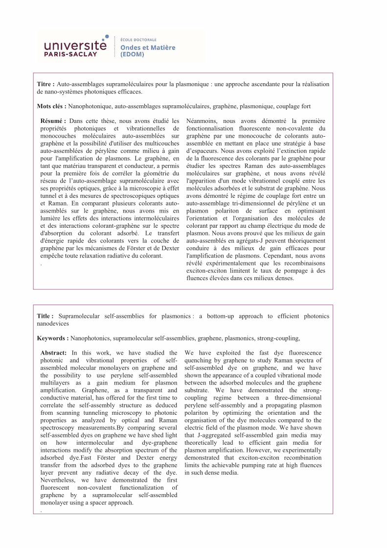
Titre : Auto-assemblages supramoléculaires pour la plasmonique : une approche ascendante pour la réalisation
de nano-systèmes photoniques efficaces.
Mots clés : Nanophotonique, auto-assemblages supramoléculaires, graphène, plasmonique, couplage fort
Résumé : Dans cette thèse, nous avons étudié les
propriétés photoniques et vibrationnelles de
monocouches moléculaires auto-assemblées sur
graphène et la possibilité d'utiliser des multicouches
auto-assemblées de pérylène comme milieu à gain
pour l'amplification de plasmons. Le graphène, en
tant que matériau transparent et conducteur, a permis
pour la première fois de corréler la géométrie du
réseau de l’auto-assemblage supramoléculaire avec
ses propriétés optiques, grâce à la microscopie à effet
tunnel et à des mesures de spectroscopiques optiques
et Raman. En comparant plusieurs colorants auto-
assemblés sur le graphène, nous avons mis en
lumière les effets des interactions intermoléculaires
et des interactions colorant-graphène sur le spectre
d'absorption du colorant adsorbé. Le transfert
d'énergie rapide des colorants vers la couche de
graphène par les mécanismes de Förster et de Dexter
empêche toute relaxation radiative du colorant.
.
Néanmoins, nous avons démontré la première
fonctionnalisation fluorescente non-covalente du
graphène par une monocouche de colorants auto-
assemblée en mettant en place une stratégie à base
d’espaceurs. Nous avons exploité l’extinction rapide
de la fluorescence des colorants par le graphène pour
étudier les spectres Raman des auto-assemblages
moléculaires sur graphène, et nous avons révélé
l'apparition d'un mode vibrationnel couplé entre les
molécules adsorbées et le substrat de graphène. Nous
avons démontré le régime de couplage fort entre un
auto-assemblage tri-dimensionnel de pérylène et un
plasmon polariton de surface en optimisant
l'orientation et l'organisation des molécules de
colorant par rapport au champ électrique du mode de
plasmon. Nous avons prouvé que les milieux de gain
auto-assemblés en agrégats-J peuvent théoriquement
conduire à des milieux de gain efficaces pour
l'amplification de plasmons. Cependant, nous avons
révélé expérimentalement que les recombinaisons
exciton-exciton limitent le taux de pompage à des
fluences élevées dans ces milieux denses.
Title : Supramolecular self-assemblies for plasmonics : a bottom-up approach to efficient photonics
nanodevices
Keywords : Nanophotonics, supramolecular self-assemblies, graphene, plasmonics, strong-coupling,
Abstract: In this work, we have studied the
photonic and vibrational properties of self-
assembled molecular monolayers on graphene and
the possibility to use perylene self-assembled
multilayers as a gain medium for plasmon
amplification. Graphene, as a transparent and
conductive material, has offered for the first time to
correlate the self-assembly structure as deduced
from scanning tunneling microscopy to photonic
properties as analyzed by optical and Raman
spectroscopy measurements.By comparing several
self-assembled dyes on graphene we have shed light
on how intermolecular and dye-graphene
interactions modify the absorption spectrum of the
adsorbed dye.Fast Förster and Dexter energy
transfer from the adsorbed dyes to the graphene
layer prevent any radiative decay of the dye.
Nevertheless, we have demonstrated the first
fluorescent non-covalent functionalization of
graphene by a supramolecular self-assembled
monolayer using a spacer approach.
.
We have exploited the fast dye fluorescence
quenching by graphene to study Raman spectra of
self-assembled dye on graphene, and we have
shown the appearance of a coupled vibrational mode
between the adsorbed molecules and the graphene
substrate. We have demonstrated the strong-
coupling regime between a three-dimensional
perylene self-assembly and a propagating plasmon
polariton by optimizing the orientation and the
organisation of the dye molecules compared to the
electric field of the plasmon mode. We have shown
that J-aggregated self-assembled gain media may
theoretically lead to efficient gain media for
plasmon amplification. However, we experimentally
demonstrated that exciton-exciton recombination
limits the achievable pumping rate at high fluences
in such dense media.

Université Paris-Saclay Espace Technologique / Immeuble Discovery
Route de l’Orme aux Merisiers RD 128 / 91190 Saint-Aubin, France


![SECTION I SUPRAMOLECULAR OBJECTS TOWARDS MULTI-TASK ... 1 Sample.pdf · ating supramolecular assemblies and applications in organic photovoltaic devices [12]. Aida and coworkers have](https://img.dokumen.tips/doc/110x75/5fca14fec301f562e47d5cf8/section-i-supramolecular-objects-towards-multi-task-1-ating-supramolecular.jpg)


![Supporting Information · Supporting Information Decamethylcucurbit[5]uril based Supramolecular Assemblies as Efficient Electrocatalysts for Oxygen Reduction Reaction Ruru Chen,ab](https://img.dokumen.tips/doc/110x75/5eaec9fbe603423ba5066208/supporting-supporting-information-decamethylcucurbit5uril-based-supramolecular.jpg)