Embed Size (px)
Citation preview
advances.sciencemag.org/cgi/content/full/1/10/e1500751/DC1
Supplementary Materials for
Uniform metal nanostructures with long-range order via three-step
hierarchical self-assembly
Denise J. Erb, Kai Schlage, Ralf Röhlsberger
Published 6 November 2015, Sci. Adv. 1, e1500751 (2015)
DOI: 10.1126/sciadv.1500751
The PDF file includes:
Fig. S1. AFM micrographs illustrating the dependence of the degree of lateral
domain ordering on the ratio of diblock copolymer film thickness to substrate
facet height.
Fig. S2. Large-area AFM scans of highly ordered metal nanostructure patterns.
Fig. S3. Experimental data and simulations of GISAXS patterns for hexagonal Fe
nanodot array growing at room temperature.
Fig. S4. Experimental data and simulations of GISAXS patterns for hexagonal Fe
nanodot array growing at 170°C.
Table S1. Compositional properties of the diblock copolymers used.
Table S2. List of apparatus and duration of individual process steps. Discussion of
nanopattern yield.

Fig. S1. AFM micrographs illustrating the dependence of the degree of lateral domain
ordering on the ratio of diblock copolymer film thickness and substrate facet height.
If d/h is too low, the substrate facets deform the surface of the diblock copolymer film. If d/h is
too high, the guiding effect of the substrate topography and thus the long-range lateral domain
ordering in the copolymer film is lost. Insets show fast Fourier transformations of the height
information.
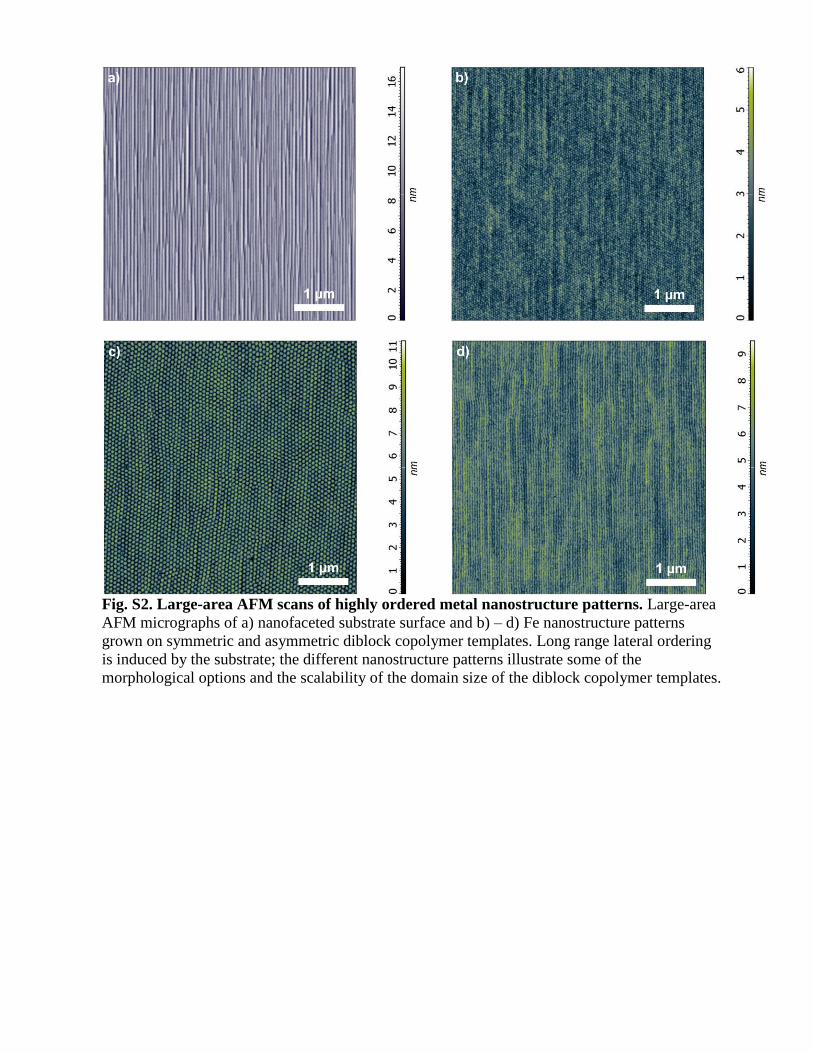
Fig. S2. Large-area AFM scans of highly ordered metal nanostructure patterns. Large-area
AFM micrographs of a) nanofaceted substrate surface and b) – d) Fe nanostructure patterns
grown on symmetric and asymmetric diblock copolymer templates. Long range lateral ordering
is induced by the substrate; the different nanostructure patterns illustrate some of the
morphological options and the scalability of the domain size of the diblock copolymer templates.

Fig. S3. Experimental data and simulations of GISAXS patterns for hexagonal Fe nanodot
array growing at room temperature. Sections in qy and qz direction through a sequence of
GISAXS patterns, recorded in-situ during Fe nanodot growth at room temperature, with
simulations (red solid lines). Labels indicate the elapsed Fe deposition time.

Fig. S4. Experimental data and simulations of GISAXS patterns for hexagonal Fe nanodot
array growing at 170C. Sections in qy and qz direction through a sequence of GISAXS
patterns, recorded in-situ during Fe nanodot growth at 170 °C, with simulations (red solid lines).
Labels indicate the elapsed Fe deposition time.
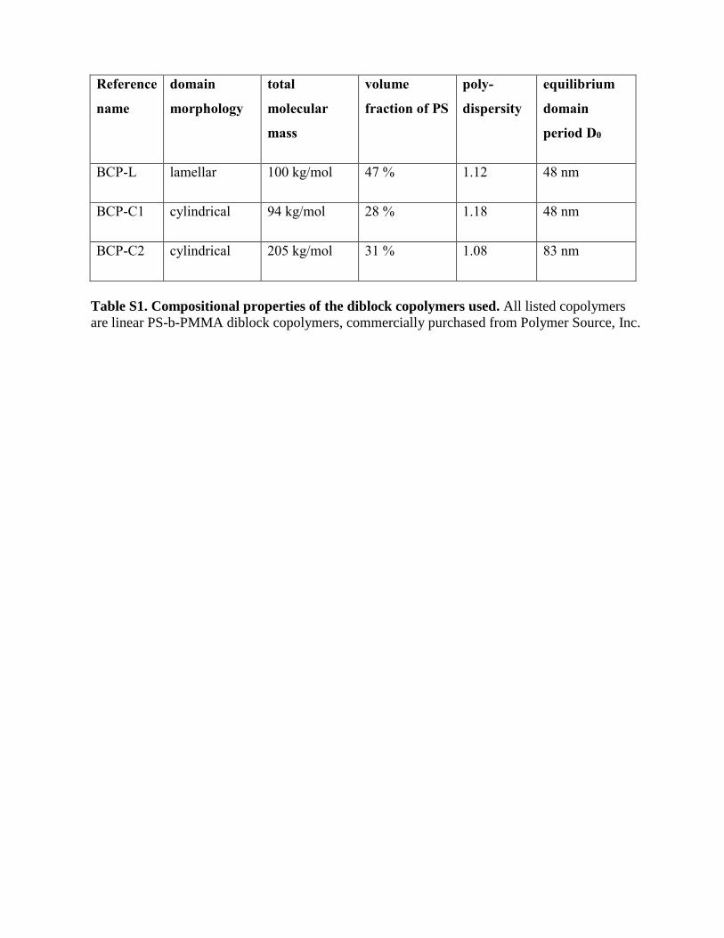
Reference
name
domain
morphology
total
molecular
mass
volume
fraction of PS
poly-
dispersity
equilibrium
domain
period D0
BCP-L lamellar 100 kg/mol 47 % 1.12 48 nm
BCP-C1 cylindrical 94 kg/mol 28 % 1.18 48 nm
BCP-C2 cylindrical 205 kg/mol 31 % 1.08 83 nm
Table S1. Compositional properties of the diblock copolymers used. All listed copolymers
are linear PS-b-PMMA diblock copolymers, commercially purchased from Polymer Source, Inc.
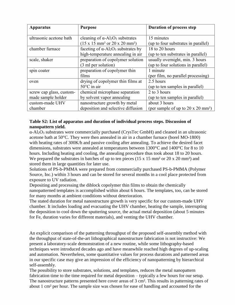
Apparatus
Purpose Duration of process step
ultrasonic acetone bath cleaning of α-Al2O3 substrates
(15 x 15 mm² or 20 x 20 mm²)
15 minutes
(up to four substrates in parallel)
chamber furnace
faceting of α-Al2O3 substrates by
high-temperature annealing in air
18 to 20 hours
(up to ten substrates in parallel)
scale, shaker preparation of copolymer solution
(3 ml per solution)
usually overnight, min. 3 hours
(up to four solutions in parallel)
spin coater preparation of copolymer thin
films
1 minute
(per film, no parallel processing)
oven drying of copolymer thin films at
50°C in air
2.5 hours
(up to ten samples in parallel)
screw cap glass, custom-
made sample holder
chemical microphase separation
by solvent vapor annealing
2 to 3 hours
(up to ten samples in parallel)
custom-made UHV
chamber
nanostructure growth by metal
deposition and selective diffusion
about 3 hours
(per sample of up to 20 x 20 mm²)
Table S2: List of apparatus and duration of individual process steps. Discussion of
nanopattern yield. α-Al2O3 substrates were commercially purchased (CrysTec GmbH) and cleaned in an ultrasonic
acetone bath at 50°C. They were then annealed in air in a chamber furnace (borel MO-1800)
with heating rates of 300K/h and passive cooling after annealing. To achieve the desired facet
dimensions, substrates were annealed at temperatures between 1300°C and 1400°C for 8 to 10
hours. Including heating and cooling, the annealing procedure thus took about 18 to 20 hours.
We prepared the substrates in batches of up to ten pieces (15 x 15 mm² or 20 x 20 mm²) and
stored them in large quantities for later use.
Solutions of PS-b-PMMA were prepared from commercially purchased PS-b-PMMA (Polymer
Source, Inc.) within 3 hours and can be stored for several months in a cool place protected from
exposure to UV radiation.
Depositing and processing the diblock copolymer thin films to obtain the chemically
nanopatterned templates is accomplished within about 6 hours. The templates, too, can be stored
for many months at ambient conditions without deterioration.
The stated duration for metal nanostructure growth is very specific for our custom-made UHV
chamber. It includes loading and evacuating the UHV chamber, heating the sample, interrupting
the deposition to cool down the sputtering source, the actual metal deposition (about 5 minutes
for Fe, duration varies for different materials), and venting the UHV chamber.
An explicit comparison of the patterning throughput of the proposed self-assembly method with
the throughput of state-of-the-art lithographical nanostructure fabrication is not instructive: We
present a laboratory-scale demonstration of a new routine, while some lithography-based
techniques were introduced decades ago and have meanwhile reached high degrees of up-scaling
and automation. Nevertheless, some quantitative values for process durations and patterned areas
in our specific case may give an impression of the efficiency of nanopatterning by hierarchical
self-assembly.
The possibility to store substrates, solutions, and templates, reduces the metal nanopattern
fabrication time to the time required for metal deposition – typically a few hours for our setup.
The nanostructure patterns presented here cover areas of 3 cm². This results in patterning rates of
about 1 cm² per hour. The sample size was chosen for ease of handling and accounted for the

dimensions of the available fabrication and characterization devices. Since the proposed routine
employs exclusively self-assembly processes, the samples can in principle be scaled up to much
larger sizes, achieving even larger patterning rates without increasing duration or complexity of
the preparation procedure. On a laboratory scale, sample sizes of about 10 x 10 cm² are
conceivable. In an industrial context, technical equipment optimized for high throughput, such as
automated spin coaters, large-volume furnaces, or inline sputtering systems would further
increase the patterning rate. Combining both approaches – increasing the sample size and
employing high-throughput fabrication devices – can result in an increase of the patterning rate
to the order of magnitude of 1000 cm² per hour or more.


![[Supplementary materials]](https://img.dokumen.tips/doc/110x75/56816583550346895dd82b8a/supplementary-materials-56cd0e37cc26b.jpg)