Embed Size (px)
Citation preview
MAHARASHTRASTATE BOARD OF TECHNICAL EDUCATION (Autonomous)
(ISO/IEC - 27001 - 2005 Certified)
Page1
MODEL ANSWER SUMMER– 17 EXAMINATION Subject Title: Basic Electronics Subject Code: Important Instructions to examiners:
1) The answers should be examined by key words and not as word-to-word as given in the model answer scheme.
2) The model answer and the answer written by candidate may vary but the examiner may try to assess the understanding level of the candidate.
3) The language errors such as grammatical, spelling errors should not be given more Importance (Not applicable for subject English and Communication Skills.
4) While assessing figures, examiner may give credit for principal components indicated in the figure. The figures drawn by candidate and model answer may vary. The examiner may give credit for anyequivalent figure drawn.
5) Credits may be given step wise for numerical problems. In some cases, the assumed constant values may vary and there may be some difference in the candidate’s answers and model answer.
6) In case of some questions credit may be given by judgement on part of examiner of relevant answer based on candidate’s understanding.
7) For programming language papers, credit may be given to any other program based on equivalent concept.
Q.
No.
Sub
Q.N.
Answer Marking
Scheme
Q.1 Attempt any ten : 20-Total
Marks
a) Define :
i) Active components ii) Passive components.
2M
Ans: Active components : The electrical components which are capable of amplifying or processing electrical signals are called active components. Example: Diode, Transistor etc.
Passive components: The electrical components which are not capable of amplifying or
processing electrical signals are called active components. Example: Inductor, Capacitor,
Resistor etc.
1M
Each
b) Draw the symbol of
i) N-channel JFET ii) P-channel JFET.
2M
Ans: Diagram :
1M
Each
17213XXXXX
MAHARASHTRASTATE BOARD OF TECHNICAL EDUCATION (Autonomous)
(ISO/IEC - 27001 - 2005 Certified)
Page2
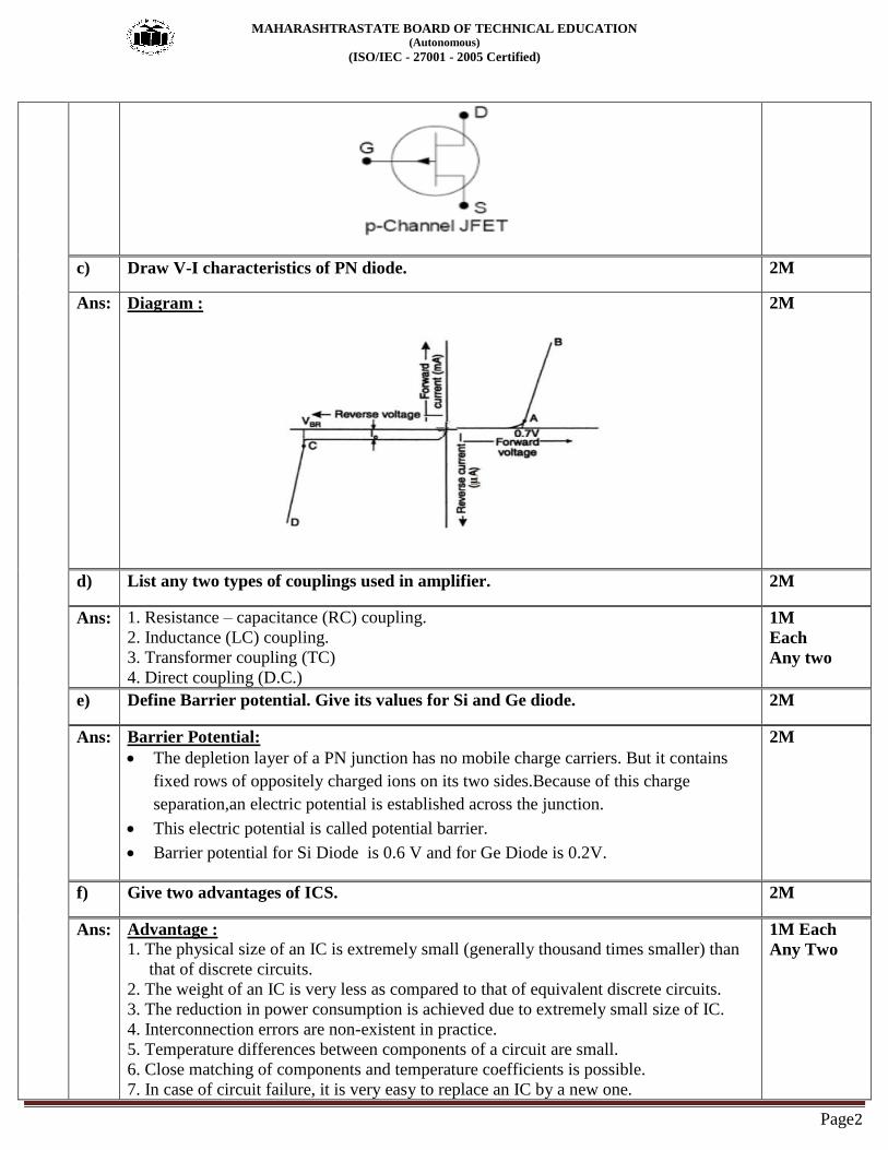
c) Draw V-I characteristics of PN diode. 2M
Ans: Diagram :
2M
d) List any two types of couplings used in amplifier. 2M
Ans: 1. Resistance – capacitance (RC) coupling. 2. Inductance (LC) coupling.
3. Transformer coupling (TC) 4. Direct coupling (D.C.)
1M
Each
Any two
e) Define Barrier potential. Give its values for Si and Ge diode. 2M
Ans: Barrier Potential:
The depletion layer of a PN junction has no mobile charge carriers. But it contains
fixed rows of oppositely charged ions on its two sides.Because of this charge
separation,an electric potential is established across the junction.
This electric potential is called potential barrier.
Barrier potential for Si Diode is 0.6 V and for Ge Diode is 0.2V.
2M
f) Give two advantages of ICS. 2M
Ans: Advantage :
1. The physical size of an IC is extremely small (generally thousand times smaller) than
that of discrete circuits. 2. The weight of an IC is very less as compared to that of equivalent discrete circuits. 3. The reduction in power consumption is achieved due to extremely small size of IC. 4. Interconnection errors are non-existent in practice. 5. Temperature differences between components of a circuit are small. 6. Close matching of components and temperature coefficients is possible.
7. In case of circuit failure, it is very easy to replace an IC by a new one.
1M Each
Any Two
MAHARASHTRASTATE BOARD OF TECHNICAL EDUCATION (Autonomous)
(ISO/IEC - 27001 - 2005 Certified)
Page3
8. Active devices can be generously used as they are cheaper than passive components.
g) Give necessity of filters in DC power supply. 2M
Ans: Need of the filter: The output of a rectifier contains ac and dc components. If such a dc
is applied in an electronic circuit, it will produce noise and therefore to keep the ac
components away from the load, filter circuits are used, which removes the ac
components and allows only dc components to reach the load.
2M
h) Define transconductance of JFET. 2M
Ans: Transconductance: Transconductance is defined as the ratio of change in Drain current (∆ID) to change in
Gate to Source Voltage (∆VGS) at a constant VDS.
2M
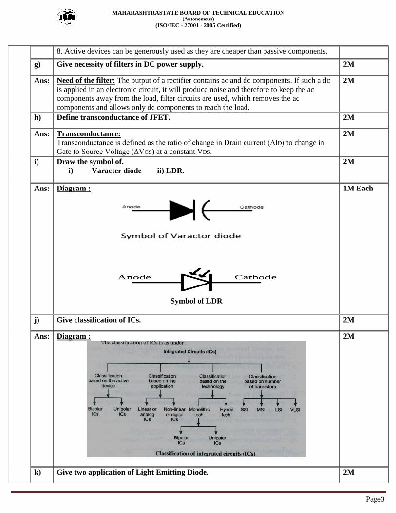
i) Draw the symbol of.
i) Varacter diode ii) LDR.
2M
Ans: Diagram :
Symbol of LDR
1M Each
j) Give classification of ICs. 2M
Ans: Diagram :
2M
k) Give two application of Light Emitting Diode. 2M

MAHARASHTRASTATE BOARD OF TECHNICAL EDUCATION (Autonomous)
(ISO/IEC - 27001 - 2005 Certified)
Page4
Ans: 1. Infra-red LEDs are used in burglar alarm systems.
2. For solid state video displays which are rapidly replacing CRT.
3. An image sensing circuit for picture phones‟
4. In array of different types for displaying alpha-numeric characters.
2M
Any two
l) Enlist two examples of non linear resistors. 2M
Ans: Examples of nonlinear resistors are: 1. Thermistor
2. LDR
3. VDR
1M Each
Q 2 Attempt any four : 16M
a) State any four applications of electronics in day to day life. 4M
Ans: Communication and Entertainment : a) Wire communication or Line communication.
Example : Telegraphy, Telephony, Telex and
Teleprinter.
b) Wireless communication. Example : radio broadcasting, TV broadcasting, satellite communication.
Defense : The most important application is RADAR.
Industrial Applications : Electronic circuits are used to control thickness, quality,
weight and moisture. They are also used to amplify weak signals.
Medical sciences : Electronics helps doctors and scientists in the diagnosis and
treatment of various diseases. Eg. X-rays, ECG, Oscillographs and Short-wave diathermy units.
Instrumentation : Instrumentation plays very vital role in research field and industry. Eg. Cathode Ray Oscilloscope (CRO), Frequency counter, Signal generator and Strain
gauges.
1M Each
Any Four
Points
b) Draw symbol of Zener Diode. Draw and explain its V-I characteristics. 4M
Ans: Symbol :
1M

MAHARASHTRASTATE BOARD OF TECHNICAL EDUCATION (Autonomous)
(ISO/IEC - 27001 - 2005 Certified)
Page5
Diagram :
Explaination:
The characteristics are similar to that of an ordinary silicon PN junction diode.
It indicates that the forward current is very small for voltages below knee voltage and
large forvoltages above knee (i.e. cut in) voltage.
The reverse characteristics curve indicates that negligible reverse saturation current flows
until wereach the breakdown (i.e. Zener) voltage Vz .
The breakdown has a very sharp knee, followed by an almost vertical increase in reverse
current.
The voltage across the zener diode is approximately constant and equal to Zener voltage
VZ over mostof the zener breakdown region.
It will come out of the breakdown region, when the applied reverse voltage is reduced
below the Zener breakdown voltage
1 ½M
1 ½M
c) Draw neat sketch of NPN Transistor. Describe its working. 4M
Ans: Diagram:
2M
MAHARASHTRASTATE BOARD OF TECHNICAL EDUCATION (Autonomous)
(ISO/IEC - 27001 - 2005 Certified)
Page6
Working
2M
d) Derive relation between α and β. 4M
Ans: relation between α and β:
We know, IE = IB + IC
Dividing the above equation on both sides by IC,
IE/IC = IB/IC + 1 Since IC/IE = α and IB/IC = β So, IE/IC = 1/ α and IC/IB = 1/β Therefore, 1/ α = 1/β + 1 Or 1/ α = 1+β / β
Therefore, α = β /(1+β) The above expression may be written as
α ( 1+β ) = β α + α β = β
α = β – αβ = β (1 – α) Therefore, β = α /(1 – α)
1M
1M
1M
1M
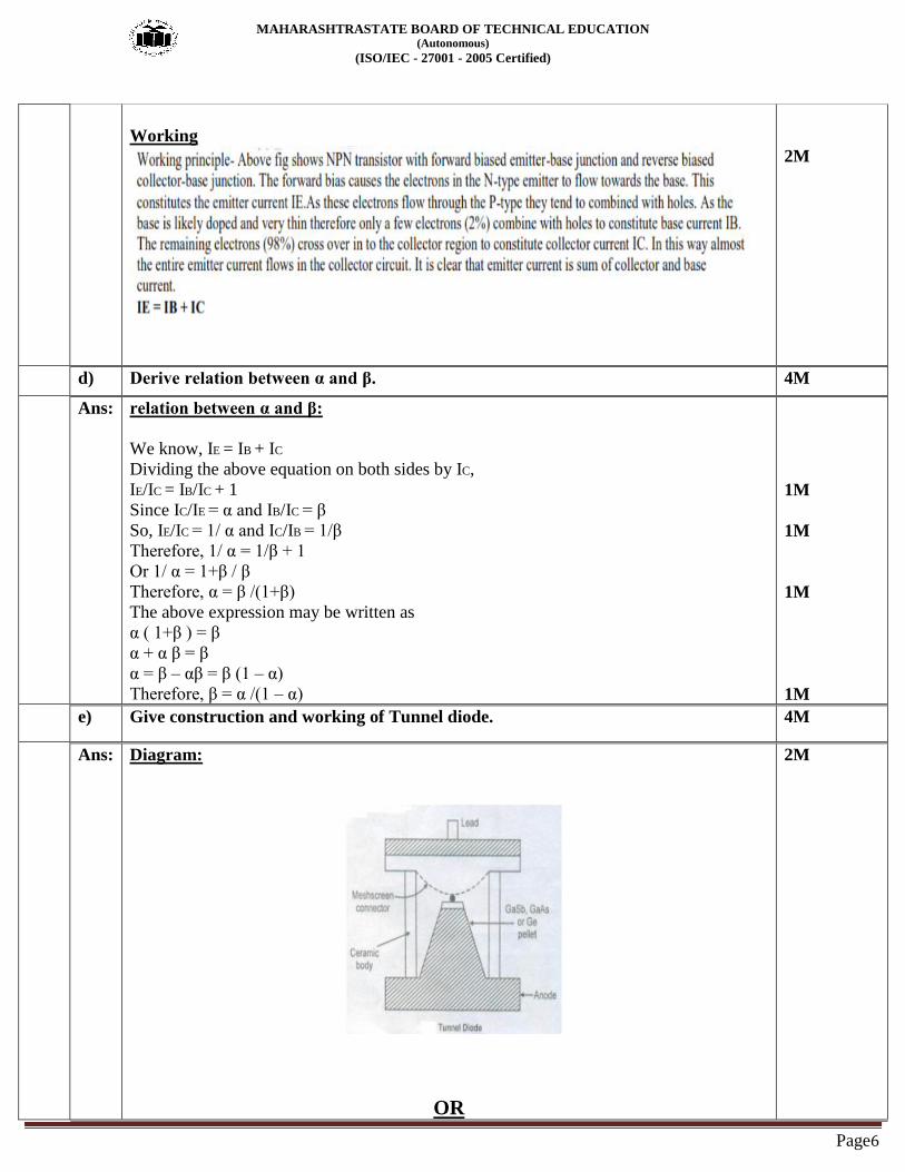
e) Give construction and working of Tunnel diode. 4M
Ans: Diagram:
OR
2M
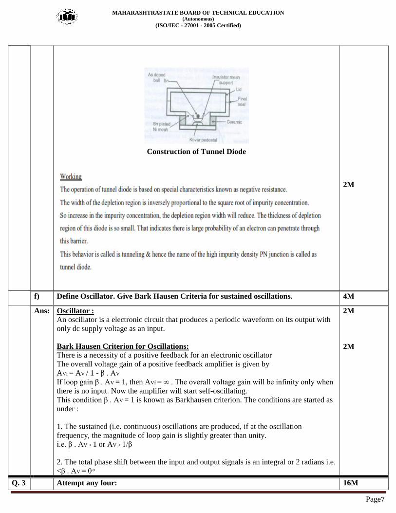
MAHARASHTRASTATE BOARD OF TECHNICAL EDUCATION (Autonomous)
(ISO/IEC - 27001 - 2005 Certified)
Page7
Construction of Tunnel Diode
2M
f) Define Oscillator. Give Bark Hausen Criteria for sustained oscillations. 4M
Ans: Oscillator : An oscillator is a electronic circuit that produces a periodic waveform on its output with
only dc supply voltage as an input.
Bark Hausen Criterion for Oscillations: There is a necessity of a positive feedback for an electronic oscillator
The overall voltage gain of a positive feedback amplifier is given by AVf = AV / 1 - β . AV If loop gain β . AV = 1, then AVf = ∞ . The overall voltage gain will be infinity only when
there is no input. Now the amplifier will start self-oscillating. This condition β . AV = 1 is known as Barkhausen criterion. The conditions are started as
under :
1. The sustained (i.e. continuous) oscillations are produced, if at the oscillation
frequency, the magnitude of loop gain is slightly greater than unity. i.e. β . AV > 1 or AV > 1/β
2. The total phase shift between the input and output signals is an integral or 2 radians i.e.
<β . AV = 0
2M
2M
Q. 3 Attempt any four: 16M

MAHARASHTRASTATE BOARD OF TECHNICAL EDUCATION (Autonomous)
(ISO/IEC - 27001 - 2005 Certified)
Page8
a) Give construction and working of LDR. 4M
Ans: Construction:
Diagram :
Explanation :
The structure of a light dependent resistor consists of a light sensitive material which is
deposited on an insulating substrate such as ceramic.
The material is deposited in zigzag pattern in order to obtain the desired resistance &
power rating.
This zigzag area separates the metal deposited areas into two regions. Then the ohmic
contacts are made on the either sides of the area.
Materials normally used are cadmium sulphide, cadmium selenide, lead sulphide,
indium antimonide and cadmium sulphonide.
Working Principle:
An LDR works on the principle of photo conductivity, which is an optical phenomenon
in which the material’s resistivity reduces when the light is absorbed by the material.
When light falls i.e. when the photons fall on the device, the electrons in the valence
band of the semiconductor material are excited to the conduction band.
These photons in the incident light should have energy greater than the band gap of the
semiconductor material to make the electrons jump from the valence band to the
conduction band.
Hence when light having enough energy is incident on the device more & more electrons
are excited to the conduction band which results in large number of charge carriers.
The result of this process is more and more current starts flowing and hence it is said that
the resistance of the device has decreased.
2M
2M
b) Draw the neat sketch of common emitter amplifier. 4M
Ans: Diagram : 4M
MAHARASHTRASTATE BOARD OF TECHNICAL EDUCATION (Autonomous)
(ISO/IEC - 27001 - 2005 Certified)
Page9
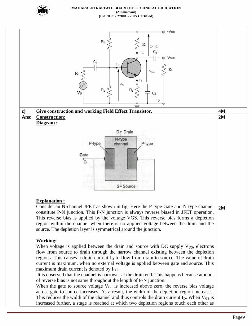
c) Give construction and working Field Effect Transistor. 4M
Ans: Construction:
Diagram :
Explanation :
Consider an N-channel JFET as shown in fig. Here the P type Gate and N type channel
constitute P-N junction. This P-N junction is always reverse biased in JFET operation.
This reverse bias is applied by the voltage VGS. This reverse bias forms a depletion
region within the channel when there is no applied voltage between the drain and the
source. The depletion layer is symmetrical around the junction.
Working:
When voltage is applied between the drain and source with DC supply VDS, electrons
flow from source to drain through the narrow channel existing between the depletion
regions. This causes a drain current ID to flow from drain to source. The value of drain
current is maximum, when no external voltage is applied between gate and source. This
maximum drain current is denoted by IDSS.
It is observed that the channel is narrower at the drain end. This happens because amount
of reverse bias is not same throughout the length of P-N junction.
When the gate to source voltage VGS is increased above zero, the reverse bias voltage
across gate to source increases. As a result, the width of the depletion region increases.
This reduces the width of the channel and thus controls the drain current ID. When VGS is
increased further, a stage is reached at which two depletion regions touch each other as
2M
2M

MAHARASHTRASTATE BOARD OF TECHNICAL EDUCATION (Autonomous)
(ISO/IEC - 27001 - 2005 Certified)
Page10
shown in the fig. This voltage between gate and source at which drain current pinches off
is called pinch off voltage and is denoted by VP.
d) Give two applications of
a) Varacter diode b) Tunnel diode.
4M
Ans: Applications of Varacter Diode:
Voltage controlled oscillators
RF filters
Tuning Circuits
High frequency amplifiers
Applications of Tunnel Diode:
High speed switches
High frequency oscillator
Micro wave generators and amplifiers
1M Each
Any Two
Points
e) Given IB =110µA, IC =2mA. For a transistor find α and β. 4M
Ans: Given IB = 110µA IC = 2mA
Calculation of α :
IE = IB + IC
IE = 110 X 10-6
+ 2 X 10-3
= 2.11 mA.
α =
α =
= 0.948.
Calculation of β :
β =
β =
= 18.2
OR
β =
=
= 18.2
2M
2M
f) Describe the need of multistage amplifier.
o/p
i/p
Find our overall gain.
4M
Ans: Need of Multistage amplifier:
Amplification of single stage is not sufficient.
Output or input impedance is not of required values.
To obtain required voltage, current and power gain.
1M Each
Any Two
Stage 1
Gain = 4
Stage 2
Gain = 5

MAHARASHTRASTATE BOARD OF TECHNICAL EDUCATION (Autonomous)
(ISO/IEC - 27001 - 2005 Certified)
Page11
Given diagram,
Stage1 Gain = AV1 = 4; Stage 2 Gain = AV2 = 5
Overall gain = AV = AV1 X AV2 = 4 X 5 = 20.
2M
Q. 4 Attempt any four : 16M
a) Give four applications of Schottky diode. 4M
Ans: Applications :
To rectify very high frequency signals
As a switching device in digital computers
In clipping and clamping circuits
In low power Schottky TTL circuits
In mixing and detecting circuits used in communication systems.
In low voltage power supply circuits
1M
Any Four
b) Draw the neat sketch of center tap full wave rectifier. Draw input and output
waveforms.
4M
Ans: Diagram :
Waveform:
Any Correct
diagram –
2M;
Waveform-
2M
c) Compare BJT and FET (any four points). 4M
Ans:
Sr. no. BJT JFET

MAHARASHTRASTATE BOARD OF TECHNICAL EDUCATION (Autonomous)
(ISO/IEC - 27001 - 2005 Certified)
Page12
1. It is bipolar device i.e. current
in the device is carried by
electrons and holes.
It is unipolar device i.e.
current in the device is carried
by either electrons or holes.
2. It is current controlled device
i.e. base current controls the
collector current.
It is voltage controlled device
i.e. voltage at the gate
terminal controls the amount
of current flowing through the
device.
3. Input resistance is low, of the
order of several KΩ
Input resistance is very high,
of the order of several MΩ
4. It has positive temperature
coefficient of resistance at
high current levels i.e. current
increases as the temperature
increases.
It has negative temperature
coefficient of resistance at
high current levels i.e. current
decreases as the temperature
increases.
5. It suffers from minority carrier
storage effects and therefore
has lower switching speeds
and cut-off frequency.
It does not suffer from
minority carrier storage
effects and therefore has
higher switching speeds and
cut-off frequency.
6. It is more noisy as compared
to FET.
It is less noisy.
7. It is complicated to fabricate
as an IC and occupies more
space on the IC chip.
It is much simpler to fabricate
as an IC and occupies less
space on the IC chip.
8. Thermal break down can
occur.
Thermal break down cannot
occur.
1M
Each
Any four
points
d) Draw and explain working of CLC filter. 4M
Ans: (Note any other diagram showing rectifier with filter may also be considered)
Diagram:
Explanation :
CLC filter or filter is used whenever a low output current and a high dc output voltage
is required. It consists of two capacitors C1 and C2 and an inductor L connected in the
form of Greek letter . The pulsating output from the rectifier is applied at the input
terminals of the filter.
Working:
Capacitor C1 filter: It offers a low reactance to ac component of rectifier output. This
capacitor bypasses most of the ac component to the ground, while dc component moves
2M
2M

MAHARASHTRASTATE BOARD OF TECHNICAL EDUCATION (Autonomous)
(ISO/IEC - 27001 - 2005 Certified)
Page13
towards L.
Inductor L : It offers a high reactance to the ac component of the rectifier output but zero
resistance to the dc component. Thus, it allows the dc component to pass through it, and
blocks the ac component, which could have been bypassed by the capacitor C1.
Capacitor C2 : This works similar to C1. It bypasses the ac component of rectifier output,
which could not be blocked by Inductor L. Thus only dc component is available at the
output.
The ripple factor is given by =
e) Draw the neat sketch of two stage transformer coupled amplifier. 4M
Ans: Diagram :
4M
f) Draw and explain construction and working of crystal oscillator circuit. 4M
Ans: Diagram :
Explanation:
A piezoelectric quartz crystal is used as in Crystal Oscillators.
Piezoelectric effect : when ac voltage applied across the quartz crystal, it vibrates at
the frequency of the applied voltage. Conversely, if a mechanical force is applied to
vibrate a quartz crystal, it generates an a.c. output.
2M
2M
MAHARASHTRASTATE BOARD OF TECHNICAL EDUCATION (Autonomous)
(ISO/IEC - 27001 - 2005 Certified)
Page14
Resistors R1, R2 and RE form the voltage divider biasing circuit, fixes the Q point.
Crystal connected as a series element in the feedback path from collector to base.
Capacitor CE parallel with RE provides low reactance path to the amplified AC signal.
RFC coil provides the dc bias also couples any ac signal from affecting the output
signal
Cc with negligible impedance blocks dc between collector and base.
Q.5 Attempt any four : 16M
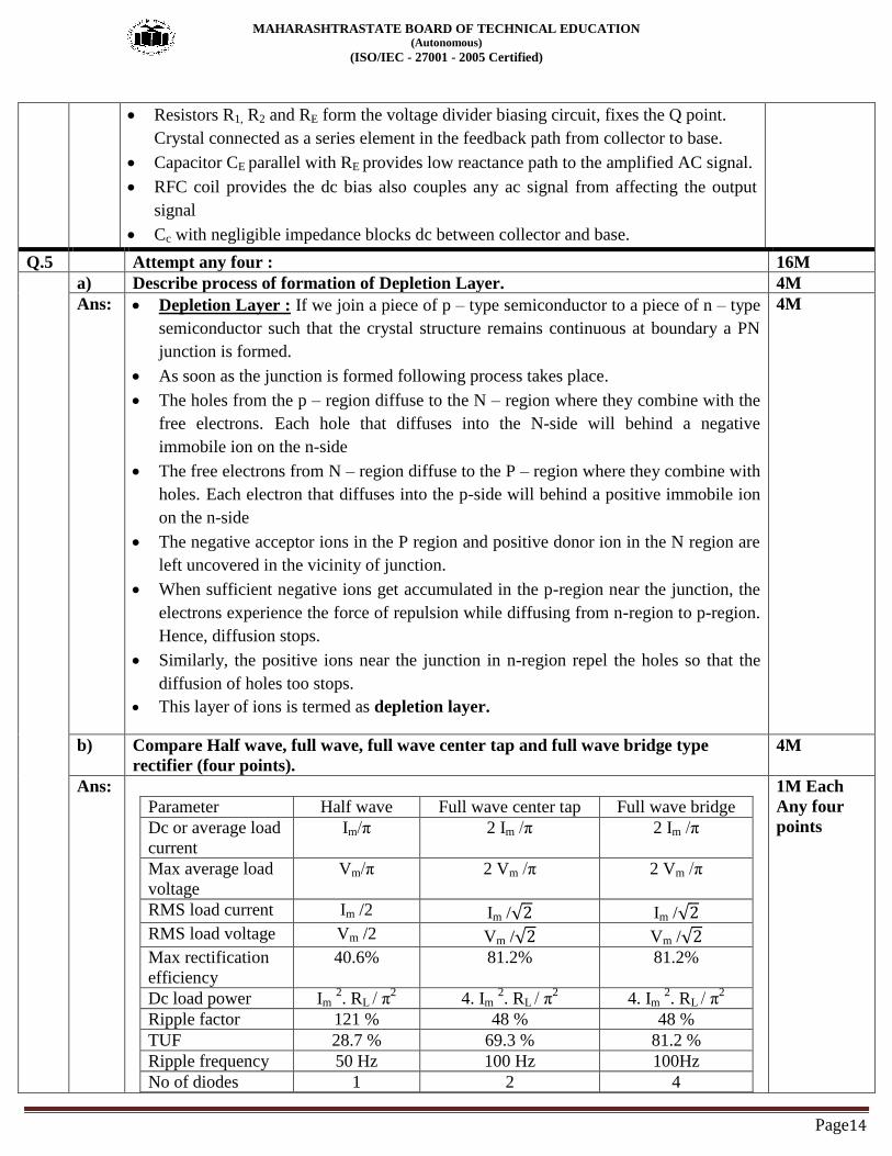
a) Describe process of formation of Depletion Layer. 4M
Ans: Depletion Layer : If we join a piece of p – type semiconductor to a piece of n – type
semiconductor such that the crystal structure remains continuous at boundary a PN
junction is formed.
As soon as the junction is formed following process takes place.
The holes from the p – region diffuse to the N – region where they combine with the
free electrons. Each hole that diffuses into the N-side will behind a negative
immobile ion on the n-side
The free electrons from N – region diffuse to the P – region where they combine with
holes. Each electron that diffuses into the p-side will behind a positive immobile ion
on the n-side
The negative acceptor ions in the P region and positive donor ion in the N region are
left uncovered in the vicinity of junction.
When sufficient negative ions get accumulated in the p-region near the junction, the
electrons experience the force of repulsion while diffusing from n-region to p-region.
Hence, diffusion stops.
Similarly, the positive ions near the junction in n-region repel the holes so that the
diffusion of holes too stops.
This layer of ions is termed as depletion layer.
4M
b) Compare Half wave, full wave, full wave center tap and full wave bridge type
rectifier (four points).
4M
Ans:
Parameter Half wave Full wave center tap Full wave bridge
Dc or average load
current
Im/π 2 Im /π 2 Im /π
Max average load
voltage
Vm/π 2 Vm /π 2 Vm /π
RMS load current Im /2 Im /√ Im /√
RMS load voltage Vm /2 Vm /√ Vm /√
Max rectification
efficiency
40.6% 81.2% 81.2%
Dc load power Im 2. RL / π
2 4. Im
2. RL / π
2 4. Im
2. RL / π
2
Ripple factor 121 % 48 % 48 %
TUF 28.7 % 69.3 % 81.2 %
Ripple frequency 50 Hz 100 Hz 100Hz
No of diodes 1 2 4
1M Each
Any four
points

MAHARASHTRASTATE BOARD OF TECHNICAL EDUCATION (Autonomous)
(ISO/IEC - 27001 - 2005 Certified)
Page15
PIV Vm 2Vm Vm
c) State and explain the operating principle of P-N junction diode under forward bias
condition.
4M
Ans: Diagram :
Explanation :
The process of applying and external voltage to a junction in such a direction that it
cancels the potential barrier, thus permitting the current flow is called as forward
biasing.
If the p-region (anode) is connected to the positive terminal of the external source
and n-side (cathode) connected to the negative terminal of the external source, then
the diode is said to be forward biased. It is shown in the fig above. Conventional
current flows in the direction opposite to the flow of electrons.
The applied forward potential establishes an electric field, which acts against the field
due to potential barrier. Therefore, the resultant field is weakened and the barrier
height is reduced at the junction. The holes and electrons are attracted to opposite
polarities of the battery and start to make efforts to cross the junction.
As potential barrier is very small, a small forward voltage is sufficient to completely
eliminate the barrier.
Once the potential barrier is eliminated by forward voltage, junction resistance
almost becomes zero and a low resistance path is established for entire circuit.
Therefore, current flowing in the circuit is called as forward current.
2M
2M
d) Give construction of Bistable multivibrator using transistor. 4M
Diagram :
4M
MAHARASHTRASTATE BOARD OF TECHNICAL EDUCATION (Autonomous)
(ISO/IEC - 27001 - 2005 Certified)
Page16
e) List two advantages and disadvantages of R-C coupled amplifier. 4M
Advantage
Most convenient and least expensive
Wide frequency response and large bandwidth
Provide excellent audio fidelity
Provides less frequency distortion.
Disadvantage
Voltage gain reduces as low frequency
Overall gain of amplifier is comparatively less
Provides poor impedance matching between amplifier stage.
Tendency to become noisy with age
1M Each
Any Two
1M Each
Any Two
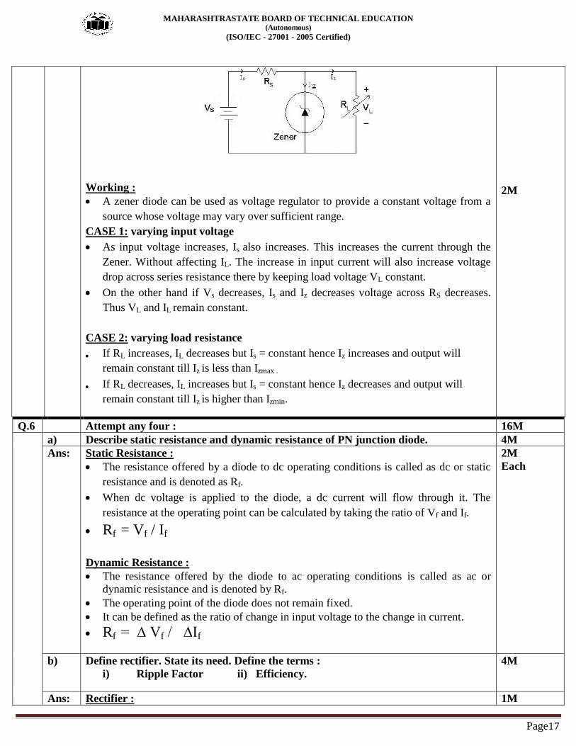
f) Describe working of Zener diode as voltage regulator. 4M
Diagram :
OR
2M
MAHARASHTRASTATE BOARD OF TECHNICAL EDUCATION (Autonomous)
(ISO/IEC - 27001 - 2005 Certified)
Page17
Working :
A zener diode can be used as voltage regulator to provide a constant voltage from a
source whose voltage may vary over sufficient range.
CASE 1: varying input voltage
As input voltage increases, Is also increases. This increases the current through the
Zener. Without affecting IL. The increase in input current will also increase voltage
drop across series resistance there by keeping load voltage VL constant.
On the other hand if Vs decreases, Is and Iz decreases voltage across RS decreases.
Thus VL and IL remain constant.
CASE 2: varying load resistance
If RL increases, IL decreases but Is = constant hence Iz increases and output will
remain constant till Iz is less than Izmax .
If RL decreases, IL increases but Is = constant hence Iz decreases and output will
remain constant till Iz is higher than Izmin.
2M
Q.6 Attempt any four : 16M
a) Describe static resistance and dynamic resistance of PN junction diode. 4M
Ans: Static Resistance :
The resistance offered by a diode to dc operating conditions is called as dc or static
resistance and is denoted as Rf.
When dc voltage is applied to the diode, a dc current will flow through it. The
resistance at the operating point can be calculated by taking the ratio of Vf and If.
Rf = Vf / If
Dynamic Resistance :
The resistance offered by the diode to ac operating conditions is called as ac or
dynamic resistance and is denoted by Rf.
The operating point of the diode does not remain fixed.
It can be defined as the ratio of change in input voltage to the change in current.
Rf = ∆ Vf / ∆If
2M
Each
b) Define rectifier. State its need. Define the terms :
i) Ripple Factor ii) Efficiency.
4M
Ans: Rectifier : 1M

MAHARASHTRASTATE BOARD OF TECHNICAL EDUCATION (Autonomous)
(ISO/IEC - 27001 - 2005 Certified)
Page18
A rectifier is a device that converts an AC signal into pulsating DC signal.
Need of rectifier :
Every electronic circuit such as an amplifier needs dc power supply for its operation.
This dc voltage has to be obtained from ac supply.
For this a.c supply voltage has to be reduced first using a step down transformer and then
converted to dc by using a rectifier.
Ripple factor :
The ratio of R.M.S value of a.c. component to the d.c. component in the rectifier output
is known as RIPPLE FACTOR.
Efficiency : It is defined as the ratio of d.c power delivered to the load to the a.c input power from the
secondary winding of the transformer.
1M
1M
1M
c) Define “Biasing of Transistor.” Explain in brief voltage divider biasing. 4M
Ans: Biasing of Transistor:
The application of a suitable Dc voltage across the transistor terminals is called biasing.
Voltage divider biasing:
Diagram :
The voltage divider is formed using external resistor R1 and R2. The voltage across
R2 forward biases the emitter junction. By proper selection of resistors R1 and R2,
the operating point of the transistor can be made independent of Ic.
In this circuit, the voltage divider holds the base voltage fixed independent of base
current provided the divider current is large compared to the base current.
However, even with a fixed base voltage, collector current varies with temperature
(for example) so an emitter resistor is added to stabilize the Q-point
2M
2M
d) Draw DC load line of transistor. Explain working of transistor as a switch. 4M
Ans: Diagram : 2M

MAHARASHTRASTATE BOARD OF TECHNICAL EDUCATION (Autonomous)
(ISO/IEC - 27001 - 2005 Certified)
Page19
Transistor as switch:
Closed switch: In saturation mode both emitter base and collector base junctions of transistor are
forward biased. In this mode transistor has a very large value of current. The transistor is
operated in this mode when it is used as a closed switch
Open switch:
In cut off mode both emitter base and collector base junctions of a transistor are reverse
biased. In this mode transistor has practically zero current. The transistor is operated in
this mode when it is used as an open switch.
2M
e) Draw and explain Drain characteristics of JFET. 4M
Ans: Diagram :
Explanation : These curves give relationship between drain current ID and drain to source voltage VDS for
different values of gate to source voltage (VGS).
2M
2M

MAHARASHTRASTATE BOARD OF TECHNICAL EDUCATION (Autonomous)
(ISO/IEC - 27001 - 2005 Certified)
Page20
Ohmic Region: Shown by curve OA in fig (b). In this region the drain current increases
linearly with the increase in drain to source voltage VDS. JFET acts as a simple resistor.
Curve AB: In this region the drain current increases slowly as compared to that in the
Ohmic Region. This is because with increase in drain to source voltage, the drain current
increases. This in turn increases the reverse bias voltage across the gate source junction.
As a result of this the depletion region grows in size, thereby reducing the effective width
of the channel.
Pinch-off Region: This region shown by BC curve. It is also called saturation Region or
constant current region. In this region, the drain current remains constant at its maximum
value. The pinch-off region is the normal operating region of JFET, when it is used in an
amplifier circuit.
Break down Region: This region shown by curve CD. In this region the drain current
increases rapidly as the drain to source voltage increases. This happens because of break
down of gate to source junction due to avalanche breakdown. The drain to source voltage
corresponding to point C is called breakdown voltage VBR
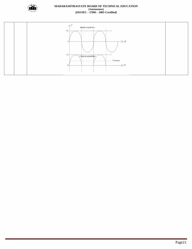
f) Draw neat sketch of half wave rectifier. List its two disadvantages. Draw input out
waveforms.
4M
Ans Half Wave Rectifier :
Diagram :
Disadvantages :
Since its ripple factor is very high, thus a big filtering circuit is required.
The efficiency is very low since output is delivered only for half the time.
Transformation Utilization factor is low.
Saturation of the transformer core results in hysteresis losses
Waveform :
2M
1M
1M
MAHARASHTRASTATE BOARD OF TECHNICAL EDUCATION (Autonomous)
(ISO/IEC - 27001 - 2005 Certified)
Page21