Embed Size (px)
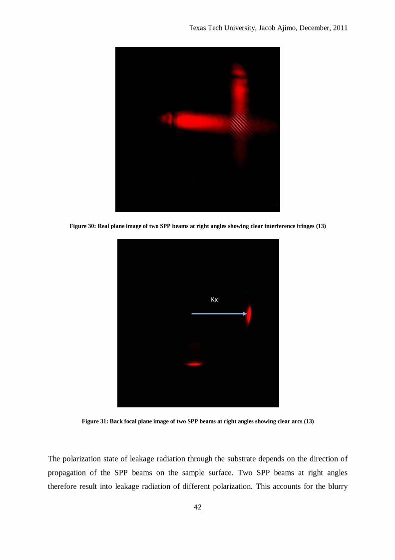
Citation preview
Study of Surface Plasmon Polariton propagation, interference and diffraction using Plasmon
Tomography
by
Jacob J. Ajimo, MS
A Dissertation
In
PHYSICS
Submitted to the Graduate Faculty
of Texas Tech University in
Partial Fulfillment of
the Requirements for
the Degree of
DOCTOR OF PHILOSOPHY
Approved
Dr. Luis Grave de Peralta
Chair of Committee
Dr. Ayrton Bernussi
Dr. Mark Holtz
Dr. Soyeun Park
Dr. Charley Myles
Peggy Gordon Miller
Dean of the Graduate School
December, 2011

© 2011, Jacob J. Ajimo

Texas Tech University, Jacob Ajimo, December, 2011
ii
Acknowledgements
This work was partially supported by the NSF CAREER Award (ECCS-0954490), U.S.
Army CERDEC contract (W15P7T-07-D-P040), and by the J. F. Maddox Foundation.

Texas Tech University, Jacob Ajimo, December, 2011
iii
Contents
Acknowledgements ....................................................................................................................... ii
Table of Figures ................................................................................................................................ v
Surface Plasmon Polaritons- an introduction ...................................................................................... 1
Chapter One ...................................................................................................................................... 3
Theory of SPPs.................................................................................................................................. 3
Single-interface mode equations .................................................................................................... 3
Multi-interface mode equation ....................................................................................................... 8
Chapter Two ................................................................................................................................... 11
Excitation of SPPs ....................................................................................................................... 11
Prism Coupling ........................................................................................................................ 11
Grating coupling ...................................................................................................................... 14
Defect Coupling....................................................................................................................... 15
Fluorescence Excitation ........................................................................................................... 15
Localized surface plasmon resonance excitation ....................................................................... 16
Endfire coupling ...................................................................................................................... 18
Chapter Three .................................................................................................................................. 19
Simulation Methods ........................................................................................................................ 19
The transfer matrix method .......................................................................................................... 19
Finite Element Analysis ............................................................................................................... 22
Chapter Four ................................................................................................................................... 24
Double spot plasmon tomography experimental set-up .................................................................... 24
Sample preparation ...................................................................................................................... 25
Imaging Techniques ........................................................................................................................ 27
SPP Propagation .............................................................................................................................. 27
Chapter Five .................................................................................................................................... 30
Polarization states of surface plasmon polariton ............................................................................... 30
Introduction ................................................................................................................................. 30
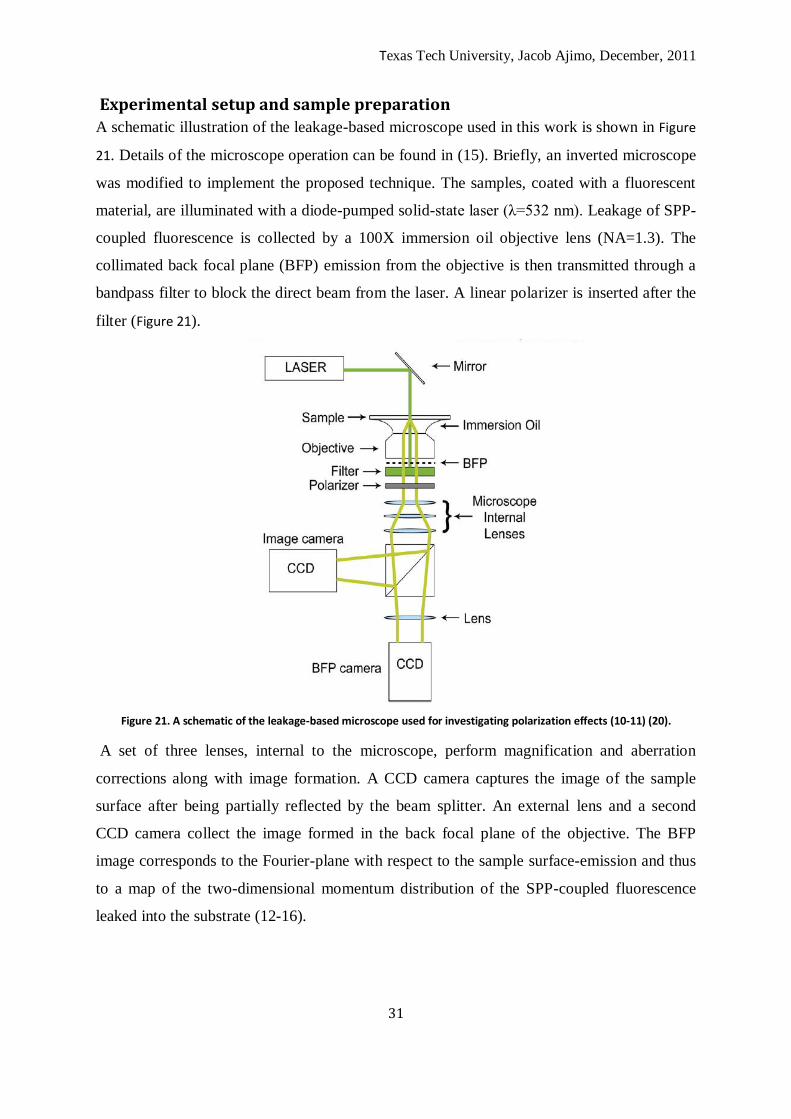
Experimental setup and sample preparation.................................................................................. 31
Experimental results and analysis ................................................................................................ 32

Texas Tech University, Jacob Ajimo, December, 2011
iv
Partial conclusions ....................................................................................................................... 39
Interference due to perpendicular SPP beams and consequences ...................................................... 40
Parallel SPP beam propagation ........................................................................................................ 44
Introduction ................................................................................................................................. 44
Experiments and discussion: ........................................................................................................ 45
Partial conclusions ....................................................................................................................... 51
Double slit diffraction of two-dimensional light using plasmon tomography .................................... 53
Introduction ................................................................................................................................. 53
Experiments ................................................................................................................................ 54
Discussion ................................................................................................................................... 57
Partial conclusions ....................................................................................................................... 60
Plasmonic implementation of a quantum eraser for imaging applications ......................................... 61
Introduction ................................................................................................................................. 61
Experiments and Discussion ........................................................................................................ 62
Partial conclusions ....................................................................................................................... 66
Conclusions ..................................................................................................................................... 66
Bibliography ................................................................................................................................... 68
Texas Tech University, Jacob Ajimo, December, 2011
v
List of Figures
Figure 1: Plasmonics compared to Electronics and Photonics in terms of their operating
speeds and critical dimension of active devices ..................................................................... 1
Figure 2: Cross-section of metal-dielectric layer showing SPPs ............................................. 7
Figure 3: Schematic of the double interface structure ........................................................... 8
Figure 4: Dispersion curves for the SP, Dielectric and Prism showing the wave vector
matching in the Kretschmann configuration. The point of intersection between the prism
light and the SP dispersion curve determines the SP excitation that satisfies the energy and
momentum conservation. ................................................................................................... 11
Figure 5: Attenuated Total Reflection set-up showing the excitation of SPPs using a prism.
........................................................................................................................................... 12
Figure 6: Reflectivity Vs angle showing the difference between SPP and total internal
reflection (TIR). .................................................................................................................. 13
Figure 7: Schematic of the Kretschmann configuration showing improvements made. Note
the high NA objective used to increase the collection angle for the leakage radiation. ........ 13
Figure 8: Sketch illustration SPP excitation by using a grating coupler. ................................ 14
Figure 9: Image of multiple SPP beams excited using defect coupling. The defect here is a
discontinuous line of PMMA deposited on a layer of gold. .................................................. 15
Figure 10: Real plane image of a sample of gold beads imaged using fluorescence excitation
with silicon dioxide as a spacer............................................................................................ 17
Figure 11: Schematic of a set-up for excitation using endfire coupling. ............................... 18
Figure 12: Simulation of reflectivity Vs angle for a thick sample showing s and p-polarized
excitation ............................................................................................................................ 21
Figure 13: Boundary mode analysis showing the location of single mode confinement........ 23
Figure 14: In-plane wave propagation for a double slit showing both interference and
diffraction of light with losses ............................................................................................. 23
Figure 15: Double spot plasmon tomography experimental set-up ....................................... 25
Figure 16: Cross-section of sample used to excite free propagating SPP beams ................... 26
Figure 17:Cross-section of sample used for exciting dielectric loaded SPP beam ................. 26
Figure 18: A: Back focal plane image of a surface plasmon beam showing the direction of
propagation (arcs) and the direct excitation (central spot), C: real plane image of SPP beams
Texas Tech University, Jacob Ajimo, December, 2011
vi
corresponding to (A), B: BFP image of a laser spot no SPP excitation, D: real plane image of
laser spot corresponding to (B). .......................................................................................... 28
Figure 19: A: Real plane image showing two SPP beams excited from a single scattering spot
obtained after inserting the spatial filter. B: Back focal plane image of (A) -the two arcs
represent the direction of propagation of the SPP beams in the momentum space. ........... 28
Figure 20: A decaying exponential fit of line profile of an SPP beam .................................... 29
Figure 21. A schematic of the leakage-based microscope used for investigating polarization
effects ................................................................................................................................. 31
Figure 22: Schematic of cross-section of sample used in the study of polarization effects ... 32
Figure 23. BFP images from a sample with an~990nm thick top layer. (a)Without polarizer
and with the transmission axis of the polarizer oriented in the (b) vertical and (c) horizontal
directions. The arrows indicate the direction of the polarizer transmission axis.................... 33
Figure 24. Illustration of the states of polarization of the leakage radiation after objective lens for excitation of (a)TE(s) and (b) TM(p) guided wave SPP mode in the sample. Double arrows point the direction of the electric field. Arrows in the sample show the direction of propagation of the excited mode. In both figures, the transmission axis of the linear polarizer is parallel to the y-axis .......................................................................................... 35
Figure 25. BFP image corresponding to DLSPPW waveguides obtained without introducing
the linear polarizer in the optical path of the leaked light ................................................... 37
Figure 26. BFP image obtained after introducing a linear polarizer with the axis of the polarizer parallel to the DLSPPW. Added arrow s indicates the direction of the axis of polarization. (b) Blow out of the right extreme of (a). ......................................................... 37
Figure 27.(a) BFP image obtained after introducing a linear polarizer with the axis of
polarization perpendicular to the DLSPPW with the arrow indicating the axis of polarization.
(b) Blow out of the right extreme of (a). .............................................................................. 38
Figure 28: Real plane image of two SPP beams at right angles showing weak interference
fringes ................................................................................................................................. 41
Figure 29: Back focal plane image of two SPP beams at right angles ................................... 41
Figure 30: Real plane image of two SPP beams at right angles showing clear interference
fringes ................................................................................................................................. 42
Figure 31: Back focal plane image of two SPP beams at right angles showing clear arcs ..... 42
Figure 32: Schematic of propagation of a SPP beam along the metal-air interface .............. 46
Figure 33: Schematic of the transversal and top views of the double-ridge pattern with the
SPPs .................................................................................................................................... 47
Texas Tech University, Jacob Ajimo, December, 2011
vii
Figure 34: Real plane (a, c) and back focal plane (b, d) images obtained by focusing two
spots simultaneously in the double-ridge scattering feature patterned on the sample surface 49
Figure 35: Schematic (not to scale) of the photon momentum distribution in diffraction by a
single-slit with (a) and (b) without walls. ............................................................................. 51
Figure 36: Schematic illustration of the fabricated sample for double-slit diffraction .......... 54
Figure 37: Surface emission images obtained (a) without and (b) blocking excited at the
metal-air interface of the sample ........................................................................................ 55
Figure 38: Fourier-plane images corresponding to the surface emission image shown in fig.
17(a). The image (a) without and (b) with added dotted circles. The smallest (largest) circle
corresponds to SPP propagating at the gold-air interface (slab). ......................................... 56
Figure 39: Fourier-plane images with auxiliary lines showing the location of diffraction
minima due to the guided modes and free propagation modes. ......................................... 57
Figure 40: Simulation of the in-plane wave propagation with losses showing the interference
of two SPP beams ............................................................................................................... 58
Figure 41: Schematic illustrations of (a) SPP collection and (b) excitation techniques used in
this work ............................................................................................................................. 62
Figure 42: SEM image of a fragment of the double-stripe structure forming each side of the L shape structure patterned on the sample surface. As shown in the inset, the width of the double-stripe structure is of ~1micrometer. Each stripe corresponds to a gold ridge of 200nm width. ...................................................................................................................... 63
Figure 43: LRM images of the sample surface emission obtained (a) without and [(b)-(d)] with a linear polarizer introduced after the oil immersion objective. Images taken with the transmission axis of the polarizer forming an angle of (b) 0, (c) 90, and (d) 45 degrees with the polarization direction of the radiation leaked along the SPP beam seen vertical in the
figures. Dashed circles have a diameter of ~5 m. They illustrate the position of the focused spots. Added discontinuous lines correspond to the L pattern used for launching the SPP beams. ................................................................................................................................ 64
Texas Tech University, Jacob Ajimo, December, 2011
1
Surface Plasmon Polaritons- an introduction
Surface Plasmon Polaritons (SPPs) are quasi two-dimensional electromagnetic waves
confined at a metal – dielectric interface and involving surface charge oscillations.
Theoretical study of these surface waves has been ongoing since the start of the century (1-3).
However, increased experimental work on the same had to wait for the development of
lithographic techniques that could enable fabrication of nano-structures. SPPs have found
immense applications in subwavelength optics, potential for use in the realization of compact
integrated optical circuits, development of chemical and biological sensors and high
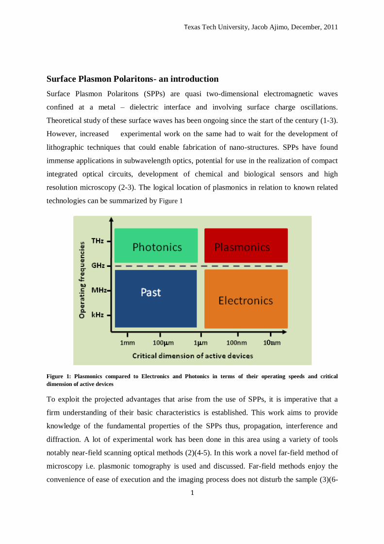
resolution microscopy (2-3). The logical location of plasmonics in relation to known related
technologies can be summarized by Figure 1
Figure 1: Plasmonics compared to Electronics and Photonics in terms of their operating speeds and critical
dimension of active devices
To exploit the projected advantages that arise from the use of SPPs, it is imperative that a
firm understanding of their basic characteristics is established. This work aims to provide
knowledge of the fundamental properties of the SPPs thus, propagation, interference and
diffraction. A lot of experimental work has been done in this area using a variety of tools
notably near-field scanning optical methods (2)(4-5). In this work a novel far-field method of
microscopy i.e. plasmonic tomography is used and discussed. Far-field methods enjoy the
convenience of ease of execution and the imaging process does not disturb the sample (3)(6-

Texas Tech University, Jacob Ajimo, December, 2011
2
10). This method also provides two image planes; the real plane and the back focal plane,
providing versatility in the image formation, signal to noise enhancement and additional
information unavailable from single plane microscopy platforms (6)(10-13).
This work is presented by laying the foundations of SPP formation in the theory of SPPs in
chapter one, excitation methods relevant to this work are presented in chapter two.
Theoretical simulations central to sample fabrication and the resulting SPP characterization is
presented in chapter three. Experimental designs employed in this work are presented in
chapter four. Chapter five has the results of specific experiments done in this work. In this
chapter a novel display of the plasmonic implementation of the quantum eraser, interference
due to parallel surface plasmon polariton beams and a discussion on the polarization states of
surface plasmon polaritons are among the topics presented. Most of this material has been
published elsewhere and are presented herein for completeness.
Texas Tech University, Jacob Ajimo, December, 2011
3
Chapter One
Theory of SPPs
Surface plasmon polaritons (SPPs) are electromagnetic excitations propagating at the
interface between a metal and a dielectric which involve electron oscillations (2-3) (11-17).
The wave equation representing these surface waves are derived from Maxwell’s equations.
The dispersion relations obtained from the wave equations are used to characterize the SPPs
thus providing information on their spatial profile and field confinement. In this section, the
mode equations for SPPs will be discussed for a single metal-dielectric interface and
extended to multilayer system similar to the samples used in this work. These mode equations
display essential features for characterizing the SPPs.
Single-interface mode equations
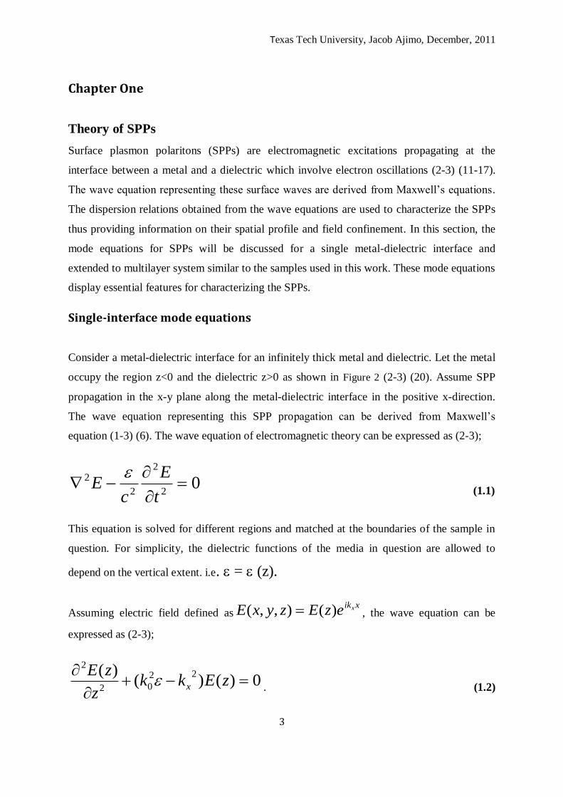
Consider a metal-dielectric interface for an infinitely thick metal and dielectric. Let the metal
occupy the region z<0 and the dielectric z>0 as shown in Figure 2 (2-3) (20). Assume SPP
propagation in the x-y plane along the metal-dielectric interface in the positive x-direction.
The wave equation representing this SPP propagation can be derived from Maxwell’s
equation (1-3) (6). The wave equation of electromagnetic theory can be expressed as (2-3);
02
2
2
2
t
E
cE
(1.1)
This equation is solved for different regions and matched at the boundaries of the sample in
question. For simplicity, the dielectric functions of the media in question are allowed to
depend on the vertical extent. i.e. = (z).
Assuming electric field defined asxikxezEzyxE )(),,( , the wave equation can be
expressed as (2-3);
0)()()( 22
02
2
zEkk
z
zEx
. (1.2)
Texas Tech University, Jacob Ajimo, December, 2011
4
This equation is valid for both the E and H fields and forms a basis for the analysis of guided
electromagnetic modes in waveguides. Assuming harmonic time dependence ( it
)
and applying Maxwell’s equations to a wave propagating in the x-direction and homogeneous
in the y-direction, the following equations are obtained (3);
zyx
yzxx
x
y
zyx
yzxx
x
y
EiHik
EiHikz
H
Eiz
H
HiEik
HiEikz
E
Hiz
E
0
0
0
0
0
0
(1.3)
This set of equations allows for two sets of self-consistent solutions with different
polarization properties of the propagating waves i.e. transverse magnetic (TM) and transverse
electric modes (TE).
For TM modes where only Ex, Ez and Hy are non-zero, the above equations reduce to (3);
yx
z
y
x
Hk
E
z
HiE
0
0
1
(1.4)
And a wave equation of the form (2) (3)
Texas Tech University, Jacob Ajimo, December, 2011
5
022
02
2
yx
yHkk
z
H
(1.5)
A similar argument can be advanced for TE modes to result in a similar wave equation for the
y-component of the E-field.
For a single interface, the TM solutions to the wave equation in both media can be derived
from the Hy (z) thus (3)
0
0)(
1
2
1
2
zeA
zeAezH
zk
zk
xik
yx
(1.6)
0
0
)(
1
2
01
11
02
22
zekA
zekA
iezE
zk
zk
xik
xx
(1.7)
01
01
)(
1
2
1
1
2
2
0
1
zek
zek
ekAzE
zk
zk
xik
xz
x
(1.8)
A generalized vector field can be used to obtain the fields in a single interface layer. This is
in the following format (2);
Texas Tech University, Jacob Ajimo, December, 2011
6
x
y
z
x
y
z
z
E
H
E
m
H
E
H
mzF 1
(1.9)
Imposing boundary conditions and continuity of the x-component of the electric and
magnetic fields at the interface, the following equations are obtained thus (3);
A1= A2 and 1
2
1
2
k
k.
These two conditions requires that Re [ifhis condition is satisfied by having a
metal and a dielectric on opposite sides of an interface supporting an SPP. The expression for
the magnetic field must satisfy the wave equation on both sides of the interface. This results
into these two equations (3);
2
2
0
22
2
1
2
0
22
1
kkk
kkk
x
x
(2.0)
where c
k
0 is the free space vector of the incident excitation photon and kx is the
component of the wave vector along the x-axis. From these two equations, the SPP dispersion
relations for a single layer interface are obtained thus (3);
21
212
0
2
kkx
(2.1)
Texas Tech University, Jacob Ajimo, December, 2011
7
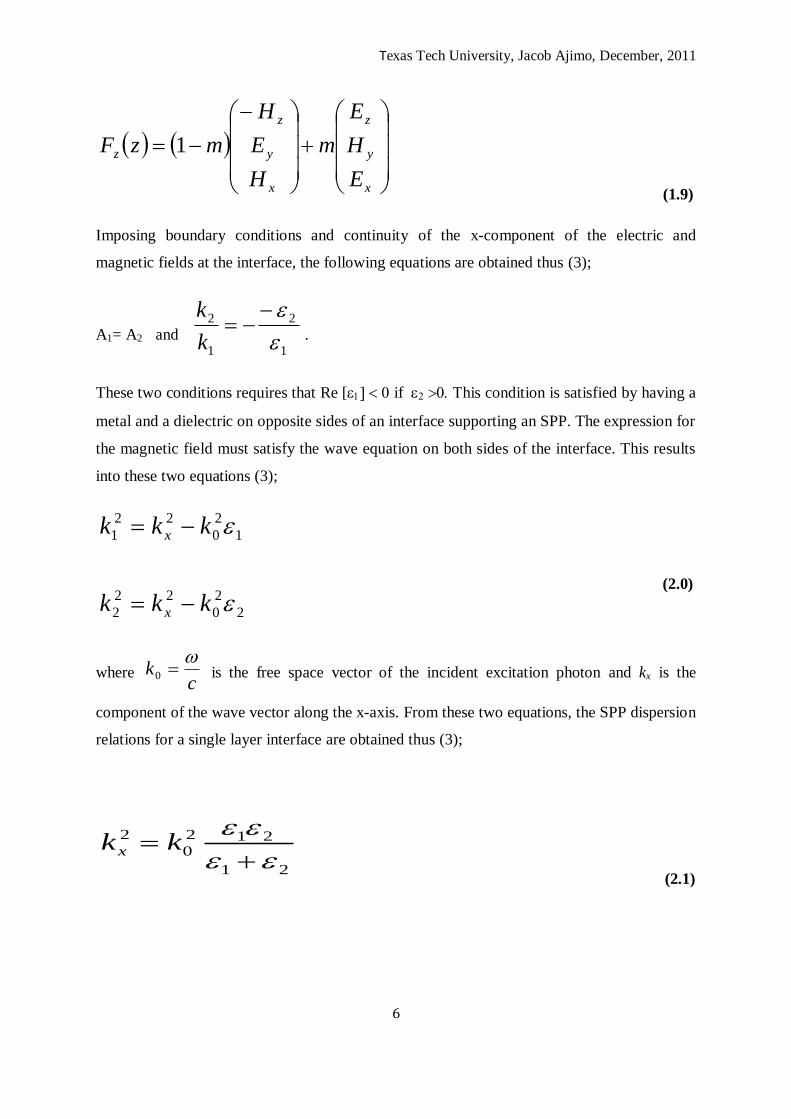
Figure 2: Cross-section of metal-dielectric layer showing SPPs (20)
The dielectric constant of metals is a complex variable. Replacing with''
2
'
2 i , equation
2.1 becomes
''2'
21
''
2
'
212
0
2
i
ikkx
(2.2)
The dispersion relation (2.2) displays SPP characteristics at a single interface along the e-
direction. A similar derivation can be obtained in the y and z directions. These equation(s)
form a basis for characterization of SPPs at a single interface.
A similar analysis for TE mode excitation reveals that wave equation with finite solutions is
not obtainable for planar confinement of SPP at a single interface.
SPPs are localized at the point of excitation with a rapidly decaying vertical extent. From the
dispersion relation (2.2) it is evident that the lateral and vertical extents of the SPPs are
dictated by the excitation and the dielectric properties of the intervening media. Sample that
support SPP propagation are typically made of multiple layers of film. The next section
therefore presents a derivation of the mode equation for a double interface medium.
Texas Tech University, Jacob Ajimo, December, 2011
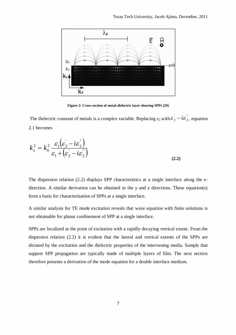
8
Multi-interface mode equation
Typical samples used for SPP involve deposition of a number of layers of material. Single
interface is a simplification of such a sample. A simple multilayer system involves three
bounding media. This can be a metal sandwiched between two dielectrics (IMI) or a
dielectric sandwiched between two metals (MIM). In this section mode equation of an IMI
multilayer system similar to that shown in the Figure 3 below will be discussed.
Figure 3: Schematic of the double interface structure
The material in the middle (guide) is made of a particular thickness less than the penetration
depth at the excitation frequency. The fields in the sample should be evanescent in both the
substrate and the cover, decaying exponentially along the direction of propagation. For an
MIM waveguide, the SPP can be excited at both surfaces of the metal. However the
characteristics of the SPPs at the two interfaces will depend on the nature of the materials
used as the substrate and the cover.
Texas Tech University, Jacob Ajimo, December, 2011
9
For a double boundary media excited by TM modes, the fields can be analyzed in three
regions thus the cover, guide and substrate.
For z > 0, the fields are (3);
zkxikx
z
zkxik
x
zkxik
y
eek
AE
eekiAE
eAeH
x
x
x
3
3
3
30
3
30
1
(2.3)
In the core region –d < z < 0 the modes at the top and bottom interface couple to give (3)
zkxikxzkxikxz
zkxikxzkxik
x
zkxikzkxik
y
eek
Deek
CE
eekk
iDeekiCE
eDeeCeH
xx
xx
xx
22
22
22
2020
2
20
2
20
1
(2.4)
Texas Tech University, Jacob Ajimo, December, 2011
10
In the region z > -d (3);
zkxikxz
zkxik
x
zkxik
y
eek
BE
eekiBE
eBeH
x
x
x
1
1
1
10
1
10
1
(2.5)
Applying the boundary conditions viz; continuity of the fields at the boundaries, a mode
equation of the components of the wave-vector can be obtained. For instance, for continuity
of Hy and Ex, the following mode equation can be obtained;
1122
1122
3322
33222 2
kk
kk
kk
kke
dk
(2.6)
This expression is valid for large d as it approximates a single layer mode equation.
When the substrate and the cover are of similar material, two possible solutions to the
dispersion equation are possible defining even and odd modes (3).
A mode equation with finite solutions can be obtained for TE mode excitation of a multilayer
film. This further confirms that a multilayer thin film supports both TE and TM modes of
excitation. An experiment done to test the polarization states of multiple modes excited on a
multilayer film confirms this claim and is described in chapter 5.
Texas Tech University, Jacob Ajimo, December, 2011
11
Chapter Two
Excitation of SPPs
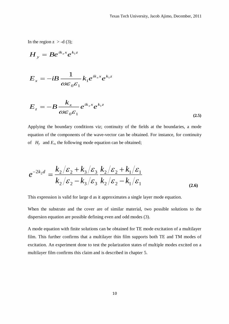
The dispersion relation for SPPs displays a mismatch of the wavevector of the incident
excitation and that of the resulting SPPs as illustrated in Figure 4. A mechanism of exciting
SPPs therefore involves coupling the excitation wavelength with the SPPs. This is done in a
number of ways;
Prism Coupling
In this method, a prism in optical contact with glass side of the sample is used to couple
excitation to the SPP. There are two known methods of SPP excitation using this method
thus; Otto configuration and the Kretschmann configuration. In the Otto configuration, the
prism is in contact with a thin layer of dielectric while a thin layer of metal is in contact with
the prism in the Kretschmann configuration. The coupling efficiency and loading is affected
by the thickness of the thin layer in optical contact with the prism. This makes the
Kretschmann configuration more versatile as a method of SPP excitation owing to the ease in
depositing a specific metal layer on the sample. Thus this section primarily discusses the
Kretschmann configuration as a method of SPP excitation.
Figure 4: Dispersion curves for the SP, Dielectric and Prism showing the wave vector matching in the Kretschmann configuration. The point of intersection between the prism light and the SP dispersion curve determines the SP excitation that satisfies the energy and momentum conservation.
0.0 0.5 1.0 1.5 2.0 2.5 3.00.0
0.2
0.4
0.6
0.8
1.0
Wavevector
No
rma
lise
dfr
equ
ency
Glass PrismDielectricSP
Texas Tech University, Jacob Ajimo, December, 2011
12
The excitation beam is made incident from the prism side and thus couples to the SPP
on the metal side of the sample as shown in Figure 5. SPPs are excited at unique resonance
angles referred to as surface plasmon resonance angles (SPRAs) at which the reflectivity is at
a minimum. At these angles, the component of the wave vector of the excitation along the
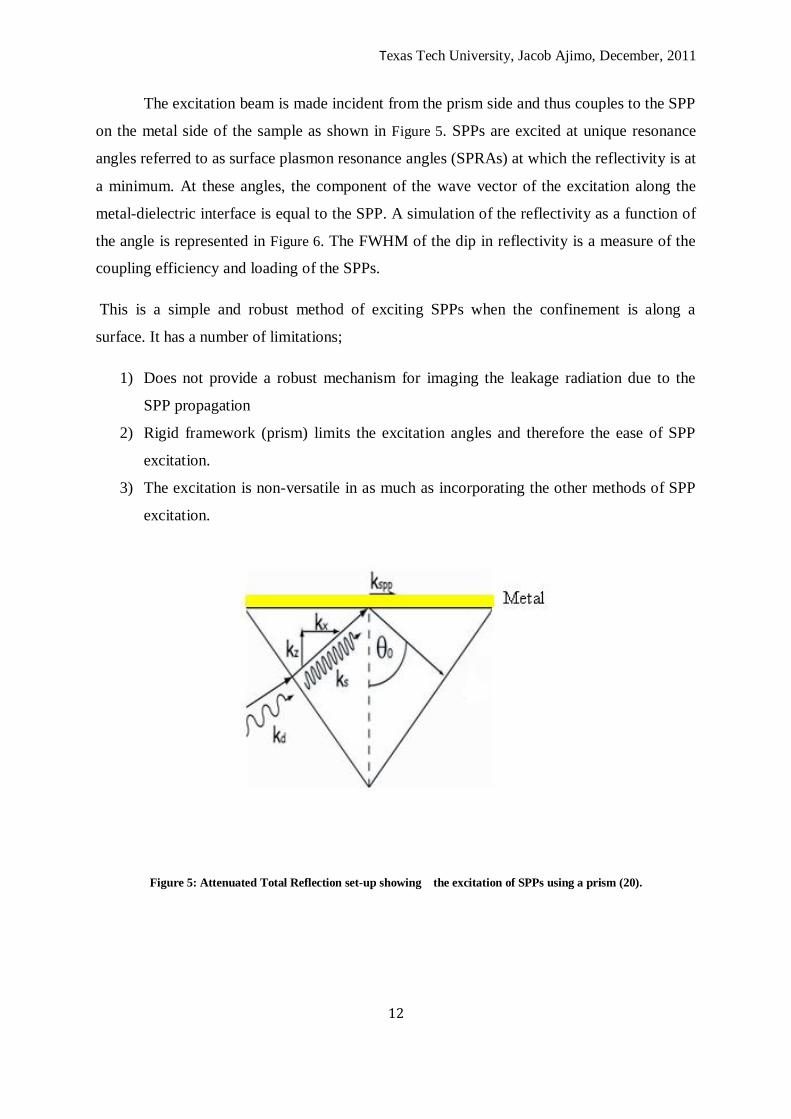
metal-dielectric interface is equal to the SPP. A simulation of the reflectivity as a function of
the angle is represented in Figure 6. The FWHM of the dip in reflectivity is a measure of the
coupling efficiency and loading of the SPPs.
This is a simple and robust method of exciting SPPs when the confinement is along a
surface. It has a number of limitations;
1) Does not provide a robust mechanism for imaging the leakage radiation due to the
SPP propagation
2) Rigid framework (prism) limits the excitation angles and therefore the ease of SPP
excitation.
3) The excitation is non-versatile in as much as incorporating the other methods of SPP
excitation.
Figure 5: Attenuated Total Reflection set-up showing the excitation of SPPs using a prism (20).
Texas Tech University, Jacob Ajimo, December, 2011
13
Figure 6: Reflectivity Vs angle showing the difference between SPP and total internal reflection (TIR) (20).
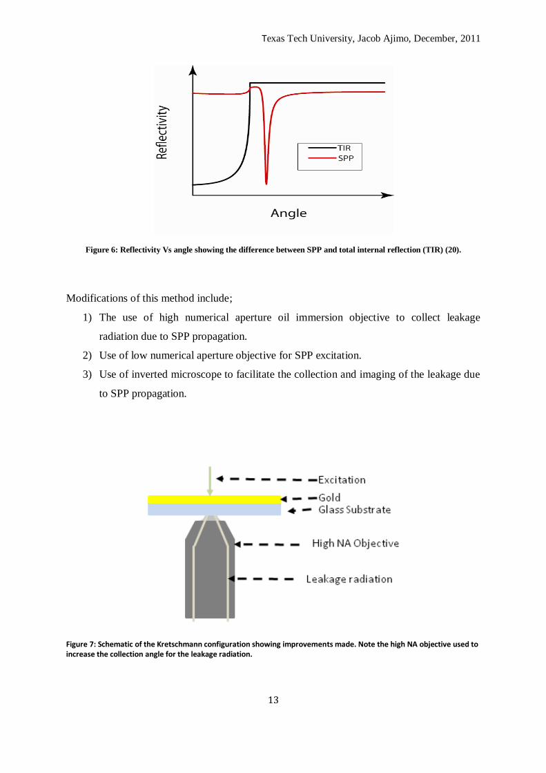
Modifications of this method include;
1) The use of high numerical aperture oil immersion objective to collect leakage
radiation due to SPP propagation.
2) Use of low numerical aperture objective for SPP excitation.
3) Use of inverted microscope to facilitate the collection and imaging of the leakage due
to SPP propagation.
Figure 7: Schematic of the Kretschmann configuration showing improvements made. Note the high NA objective used to increase the collection angle for the leakage radiation.
Texas Tech University, Jacob Ajimo, December, 2011
14
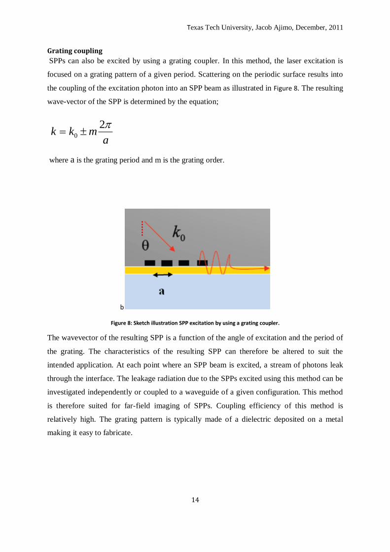
Grating coupling
SPPs can also be excited by using a grating coupler. In this method, the laser excitation is
focused on a grating pattern of a given period. Scattering on the periodic surface results into
the coupling of the excitation photon into an SPP beam as illustrated in Figure 8. The resulting
wave-vector of the SPP is determined by the equation;
a
mkk2
0
where a is the grating period and m is the grating order.
b
Figure 8: Sketch illustration SPP excitation by using a grating coupler.
The wavevector of the resulting SPP is a function of the angle of excitation and the period of
the grating. The characteristics of the resulting SPP can therefore be altered to suit the
intended application. At each point where an SPP beam is excited, a stream of photons leak
through the interface. The leakage radiation due to the SPPs excited using this method can be
investigated independently or coupled to a waveguide of a given configuration. This method
is therefore suited for far-field imaging of SPPs. Coupling efficiency of this method is
relatively high. The grating pattern is typically made of a dielectric deposited on a metal
making it easy to fabricate.
Texas Tech University, Jacob Ajimo, December, 2011
15
Defect Coupling
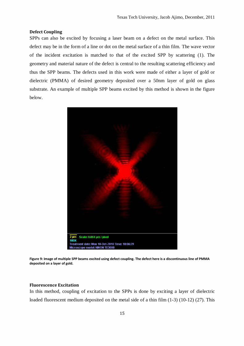
SPPs can also be excited by focusing a laser beam on a defect on the metal surface. This
defect may be in the form of a line or dot on the metal surface of a thin film. The wave vector
of the incident excitation is matched to that of the excited SPP by scattering (1). The
geometry and material nature of the defect is central to the resulting scattering efficiency and
thus the SPP beams. The defects used in this work were made of either a layer of gold or
dielectric (PMMA) of desired geometry deposited over a 50nm layer of gold on glass
substrate. An example of multiple SPP beams excited by this method is shown in the figure
below.
Figure 9: Image of multiple SPP beams excited using defect coupling. The defect here is a discontinuous line of PMMA deposited on a layer of gold.
Fluorescence Excitation
In this method, coupling of excitation to the SPPs is done by exciting a layer of dielectric
loaded fluorescent medium deposited on the metal side of a thin film (1-3) (10-12) (27). This
Texas Tech University, Jacob Ajimo, December, 2011
16
is a versatile method of SPP excitation as it allows for a selection of excitation wavelength as
well as the fluorescent medium to use. The use of quantum dots with their ensuing
advantages makes this method of excitation an attractive option for use in the future. When
white light is used, a set of filters can be used to select operating wavelengths of choice.
Fluorescence emission is in all directions in the sample. This fluorescence emission couples
to the evanescent field at the metal-dielectric interface. Radiation leaks from this interface at
an angle of surface plasmon resonance. This angle can be determined both experimentally
and through simulations. Images due to SPP propagation following fluorescence excitation
can be obtained from the leakage radiation in the real plane and the back focal plane. Real
plane image represents the actual SPP propagation as seen from leakage radiation away from
the sample while the back focal plane represents the Fourier transform of this image. For a
uniform surface, the wave-vector corresponding to this angle is unique resulting into a ring in
the back focal plane for each SPP mode supported. The fluorescent medium used in this work
is Rhodamine 6G dissolved in PMMA. The concentration and thickness of the gain medium
is carefully controlled to ensure that the desired SPP modes are supported by the resulting
film. The thickness of the layer of the gain medium is primarily controlled by the speed of
spin at the time of spin coating and the type and concentration of the PMMA used.
The back focal plane images of a uniform layer of a gain medium are used to experimentally
verify the presence of single or multiple modes on uniform surfaces. Each mode supported by
the sample is represented by a circle in the back focal plane. Real plane images from this
method of excitation provide more details on the sample features as will be discussed later in
chapter five. Combined real and back focal plane images obtained from fluorescence
excitation is useful in characterization of polarization states of the SPP excitation, imaging
periodic patterns and random patterns made on a 50nm layer of gold on a glass substrate.
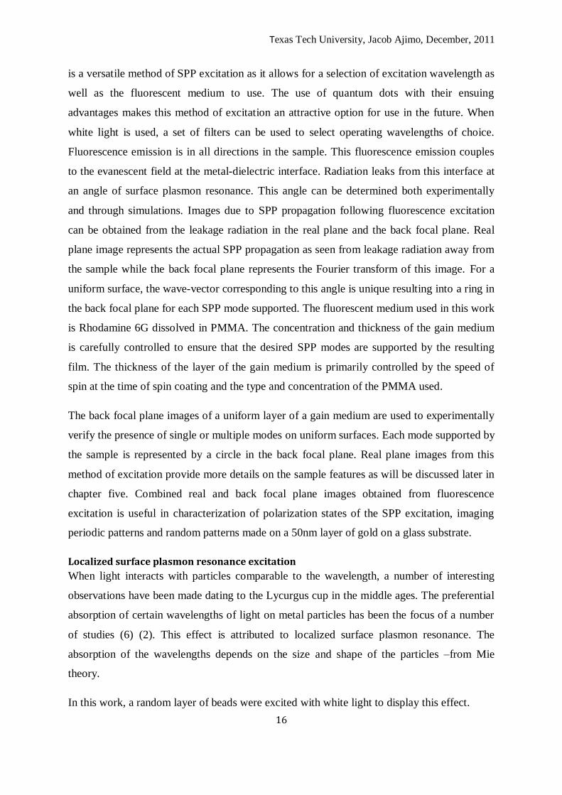
Localized surface plasmon resonance excitation
When light interacts with particles comparable to the wavelength, a number of interesting
observations have been made dating to the Lycurgus cup in the middle ages. The preferential
absorption of certain wavelengths of light on metal particles has been the focus of a number
of studies (6) (2). This effect is attributed to localized surface plasmon resonance. The
absorption of the wavelengths depends on the size and shape of the particles –from Mie
theory.
In this work, a random layer of beads were excited with white light to display this effect.
Texas Tech University, Jacob Ajimo, December, 2011
17
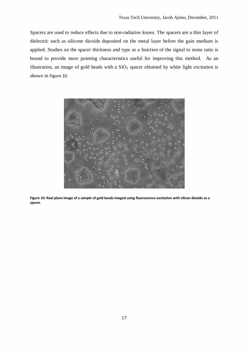
Spacers are used to reduce effects due to non-radiative losses. The spacers are a thin layer of
dielectric such as silicone dioxide deposited on the metal layer before the gain medium is
applied. Studies on the spacer thickness and type as a function of the signal to noise ratio is
bound to provide more pointing characteristics useful for improving this method. As an
illustration, an image of gold beads with a SiO2 spacer obtained by white light excitation is
shown in Figure 10.
Figure 10: Real plane image of a sample of gold beads imaged using fluorescence excitation with silicon dioxide as a spacer.
Texas Tech University, Jacob Ajimo, December, 2011
18
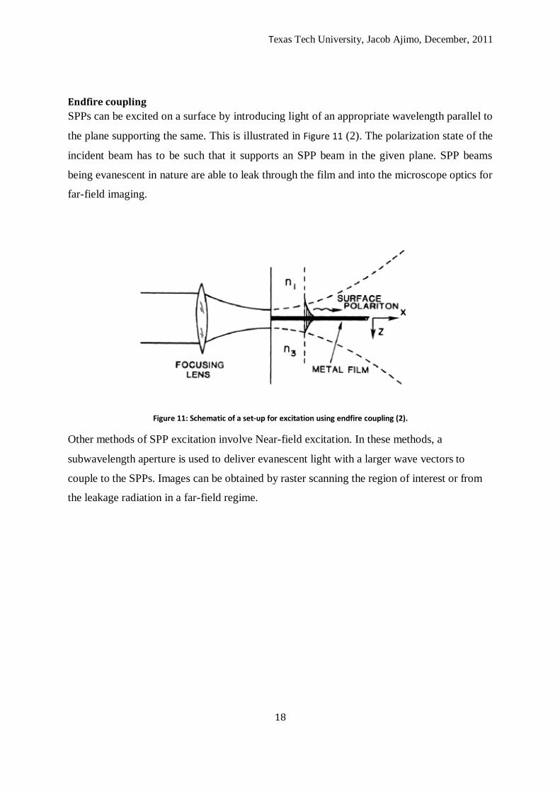
Endfire coupling
SPPs can be excited on a surface by introducing light of an appropriate wavelength parallel to
the plane supporting the same. This is illustrated in Figure 11 (2). The polarization state of the
incident beam has to be such that it supports an SPP beam in the given plane. SPP beams
being evanescent in nature are able to leak through the film and into the microscope optics for
far-field imaging.
Figure 11: Schematic of a set-up for excitation using endfire coupling (2).
Other methods of SPP excitation involve Near-field excitation. In these methods, a
subwavelength aperture is used to deliver evanescent light with a larger wave vectors to
couple to the SPPs. Images can be obtained by raster scanning the region of interest or from
the leakage radiation in a far-field regime.
Texas Tech University, Jacob Ajimo, December, 2011
19
Chapter Three
Simulation Methods
The transfer matrix method
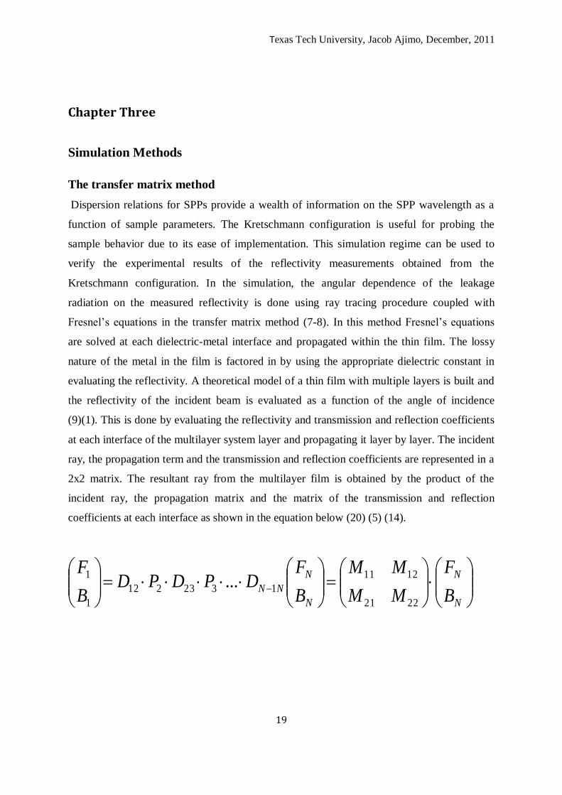
Dispersion relations for SPPs provide a wealth of information on the SPP wavelength as a
function of sample parameters. The Kretschmann configuration is useful for probing the
sample behavior due to its ease of implementation. This simulation regime can be used to
verify the experimental results of the reflectivity measurements obtained from the
Kretschmann configuration. In the simulation, the angular dependence of the leakage
radiation on the measured reflectivity is done using ray tracing procedure coupled with
Fresnel’s equations in the transfer matrix method (7-8). In this method Fresnel’s equations
are solved at each dielectric-metal interface and propagated within the thin film. The lossy
nature of the metal in the film is factored in by using the appropriate dielectric constant in
evaluating the reflectivity. A theoretical model of a thin film with multiple layers is built and
the reflectivity of the incident beam is evaluated as a function of the angle of incidence
(9)(1). This is done by evaluating the reflectivity and transmission and reflection coefficients
at each interface of the multilayer system layer and propagating it layer by layer. The incident
ray, the propagation term and the transmission and reflection coefficients are represented in a
2x2 matrix. The resultant ray from the multilayer film is obtained by the product of the
incident ray, the propagation matrix and the matrix of the transmission and reflection
coefficients at each interface as shown in the equation below (20) (5) (14).
N
N
N
N
NNB
F
MM
MM
B
FDPDPD
B
F
2221
1211
1323212
1
1...
Texas Tech University, Jacob Ajimo, December, 2011
20
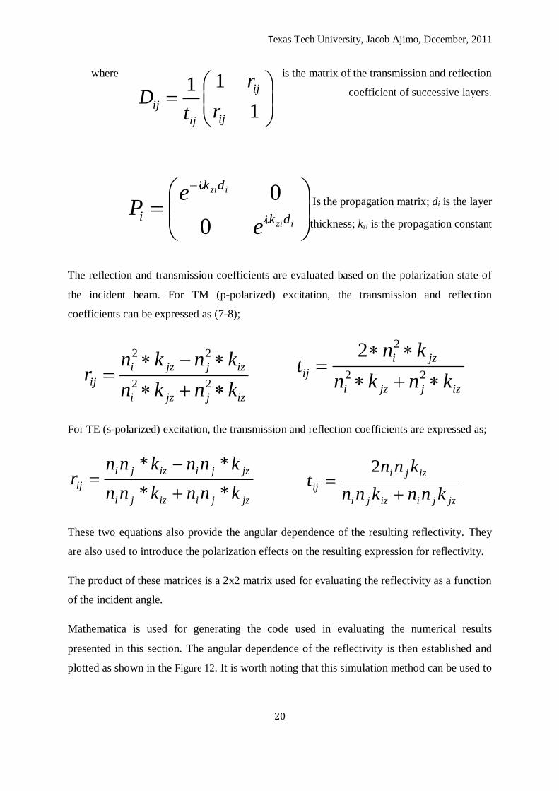
where is the matrix of the transmission and reflection
coefficient of successive layers.
Is the propagation matrix; di is the layer
thickness; kzi is the propagation constant
The reflection and transmission coefficients are evaluated based on the polarization state of
the incident beam. For TM (p-polarized) excitation, the transmission and reflection
coefficients can be expressed as (7-8);
For TE (s-polarized) excitation, the transmission and reflection coefficients are expressed as;
jzjiizji
jzjiizji
ijknnknn
knnknnr
**
**
jzjiizji
izji
ijknnknn
knnt
2
These two equations also provide the angular dependence of the resulting reflectivity. They
are also used to introduce the polarization effects on the resulting expression for reflectivity.
The product of these matrices is a 2x2 matrix used for evaluating the reflectivity as a function
of the incident angle.
Mathematica is used for generating the code used in evaluating the numerical results
presented in this section. The angular dependence of the reflectivity is then established and
plotted as shown in the Figure 12. It is worth noting that this simulation method can be used to
1
11
ij
ij
ij
ij r
r
tD
izi
izi
dk
dk
ie
eP i
i
0
0
izjjzi
izjjzi
ijknkn
knknr
22
22
izjjzi
jzi
ijknkn
knt
22
22
Texas Tech University, Jacob Ajimo, December, 2011
21
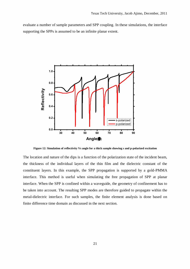
evaluate a number of sample parameters and SPP coupling. In these simulations, the interface
supporting the SPPs is assumed to be an infinite planar extent.
Figure 12: Simulation of reflectivity Vs angle for a thick sample showing s and p-polarized excitation
The location and nature of the dips is a function of the polarization state of the incident beam,
the thickness of the individual layers of the thin film and the dielectric constant of the
constituent layers. In this example, the SPP propagation is supported by a gold-PMMA
interface. This method is useful when simulating the free propagation of SPP at planar
interface. When the SPP is confined within a waveguide, the geometry of confinement has to
be taken into account. The resulting SPP modes are therefore guided to propagate within the
metal-dielectric interface. For such samples, the finite element analysis is done based on
finite difference time domain as discussed in the next section.
30 40 50 60 70 80 90
0.0
0.2
0.4
0.6
0.8
1.0
Reflectivity
Angle(
s-polarized
p-polarized
Texas Tech University, Jacob Ajimo, December, 2011
22
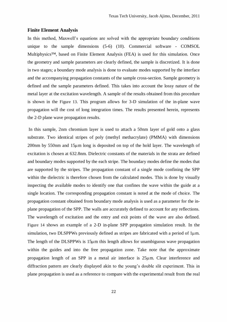
Finite Element Analysis
In this method, Maxwell’s equations are solved with the appropriate boundary conditions
unique to the sample dimensions (5-6) (10). Commercial software - COMSOL
Multiphysics™, based on Finite Element Analysis (FEA) is used for this simulation. Once
the geometry and sample parameters are clearly defined, the sample is discretized. It is done
in two stages; a boundary mode analysis is done to evaluate modes supported by the interface
and the accompanying propagation constants of the sample cross-section. Sample geometry is
defined and the sample parameters defined. This takes into account the lossy nature of the
metal layer at the excitation wavelength. A sample of the results obtained from this procedure
is shown in the Figure 13. This program allows for 3-D simulation of the in-plane wave
propagation will the cost of long integration times. The results presented herein, represents
the 2-D plane wave propagation results.
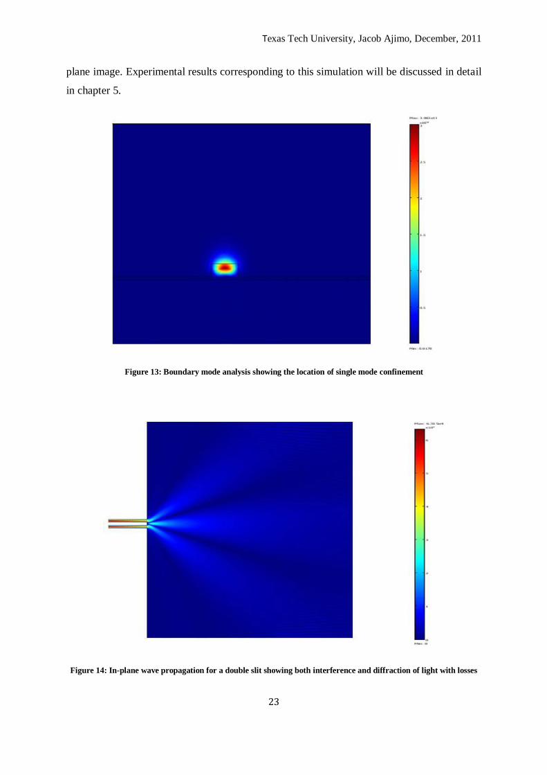
In this sample, 2nm chromium layer is used to attach a 50nm layer of gold onto a glass
substrate. Two identical stripes of poly (methyl methacrylate) (PMMA) with dimensions
200nm by 550nm and 15m long is deposited on top of the hold layer. The wavelength of
excitation is chosen at 632.8nm. Dielectric constants of the materials in the strata are defined
and boundary modes supported by the each stripe. The boundary modes define the modes that
are supported by the stripes. The propagation constant of a single mode confining the SPP
within the dielectric is therefore chosen from the calculated modes. This is done by visually
inspecting the available modes to identify one that confines the wave within the guide at a
single location. The corresponding propagation constant is noted at the mode of choice. The
propagation constant obtained from boundary mode analysis is used as a parameter for the in-
plane propagation of the SPP. The walls are accurately defined to account for any reflections.
The wavelength of excitation and the entry and exit points of the wave are also defined.
Figure 14 shows an example of a 2-D in-plane SPP propagation simulation result. In the
simulation, two DLSPPWs previously defined as stripes are fabricated with a period of 1m.
The length of the DLSPPWs is 15m this length allows for unambiguous wave propagation
within the guides and into the free propagation zone. Take note that the approximate
propagation length of an SPP in a metal air interface is 25m. Clear interference and
diffraction pattern are clearly displayed akin to the young’s double slit experiment. This in
plane propagation is used as a reference to compare with the experimental result from the real
Texas Tech University, Jacob Ajimo, December, 2011
23
plane image. Experimental results corresponding to this simulation will be discussed in detail
in chapter 5.
Figure 13: Boundary mode analysis showing the location of single mode confinement
Figure 14: In-plane wave propagation for a double slit showing both interference and diffraction of light with losses
Texas Tech University, Jacob Ajimo, December, 2011
24
Chapter Four
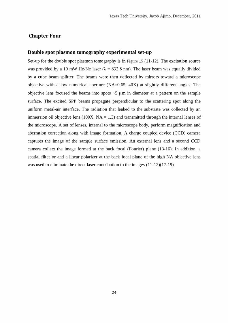
Double spot plasmon tomography experimental set-up
Set-up for the double spot plasmon tomography is in Figure 15 (11-12). The excitation source
was provided by a 10 mW He-Ne laser (λ = 632.8 nm). The laser beam was equally divided
by a cube beam splitter. The beams were then deflected by mirrors toward a microscope
objective with a low numerical aperture (NA=0.65, 40X) at slightly different angles. The
objective lens focused the beams into spots ~5 m in diameter at a pattern on the sample
surface. The excited SPP beams propagate perpendicular to the scattering spot along the
uniform metal-air interface. The radiation that leaked to the substrate was collected by an
immersion oil objective lens (100X, NA = 1.3) and transmitted through the internal lenses of
the microscope. A set of lenses, internal to the microscope body, perform magnification and
aberration correction along with image formation. A charge coupled device (CCD) camera
captures the image of the sample surface emission. An external lens and a second CCD
camera collect the image formed at the back focal (Fourier) plane (13-16). In addition, a
spatial filter or and a linear polarizer at the back focal plane of the high NA objective lens
was used to eliminate the direct laser contribution to the images (11-12)(17-19).
Texas Tech University, Jacob Ajimo, December, 2011
25
Figure 15: Double spot plasmon tomography experimental set-up
Sample preparation
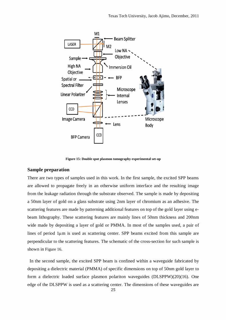
There are two types of samples used in this work. In the first sample, the excited SPP beams
are allowed to propagate freely in an otherwise uniform interface and the resulting image
from the leakage radiation through the substrate observed. The sample is made by depositing
a 50nm layer of gold on a glass substrate using 2nm layer of chromium as an adhesive. The
scattering features are made by patterning additional features on top of the gold layer using e-
beam lithography. These scattering features are mainly lines of 50nm thickness and 200nm
wide made by depositing a layer of gold or PMMA. In most of the samples used, a pair of
lines of period 1m is used as scattering center. SPP beams excited from this sample are
perpendicular to the scattering features. The schematic of the cross-section for such sample is
shown in Figure 16.
In the second sample, the excited SPP beam is confined within a waveguide fabricated by
depositing a dielectric material (PMMA) of specific dimensions on top of 50nm gold layer to
form a dielectric loaded surface plasmon polariton waveguides (DLSPPW)(20)(16). One
edge of the DLSPPW is used as a scattering center. The dimensions of these waveguides are

Texas Tech University, Jacob Ajimo, December, 2011
26
carefully simulated to ensure that they propagate the desired modes. Further simulation of the
in-plane wave propagation is also done and compared with the resulting real plane images.
For this work single mode propagation was used. The schematic of the cross-section for such
a sample is shown in Figure 17.
Figure 16: Cross-section of sample used to excite free propagating SPP beams
Figure 17:Cross-section of sample used for exciting dielectric loaded SPP beam
Texas Tech University, Jacob Ajimo, December, 2011
27
Imaging Techniques
Images presented in this work are mainly obtained by plasmon tomography. This is a far-field
method that allows for image formation in the real plane and the back focal plane. The image
at the real plane represents the surface image of the sample while the back focal plane image
represents the Fourier transform of this image. In plasmon tomography, the image is formed
by the leakage of radiation from the interface where an SPP beam is propagating. The
resolution of the resulting image depends on the SPP wavelength. The SPP wavelength
depends on the dielectric properties of the constituent materials of the thin film. This method
is therefore none diffraction limited. The dual plane provides rich data useful for sample
characterization. Additionally it provides for an indirect method of imaging without
disturbing the sample under investigation. Since it does not involve raster scanning of the
sample surface, the imaging time is short and runs no risk of damaging the sample under
investigation. A study tailored to establishing the resolution limit of this technique is
desirable and beyond the scope of this work.
SPP Propagation
Scattering was used as a method of excitation and generation of SPP beams in this work. An
incident beam of a laser (HeNe) of wavelength 632.8nm was focused on a sample as
previously described in Figure 16. The leakage radiation collected by the high numerical
aperture objective was focused onto the real plane and the BFP planes. A number of steps are
taken to improve the signal to noise ratio and hence the quality of the beam propagated.
These steps include; focusing the excitation at the center of the scattering feature,
introduction of the spatial filter to isolate the direct excitation and use of the polarizer to
eliminate spurious features in the image due to diffuse scattering. Real plane and BFP images
showing the progressive improvement in the beam quality are displayed in the next set of
figures:
Step 1: Focusing the excitation beam on the scattering center (structure).
Texas Tech University, Jacob Ajimo, December, 2011
28
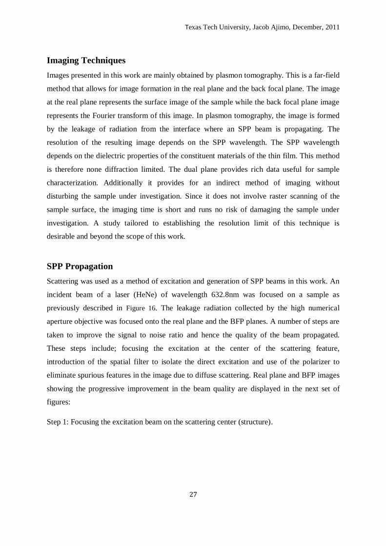
Figure 18: A: Back focal plane image of a surface plasmon beam showing the direction of propagation (arcs) and the direct excitation (central spot), C: real plane image of SPP beams corresponding to (A), B: BFP image of a laser spot no SPP excitation, D: real plane image of laser spot corresponding to (B).
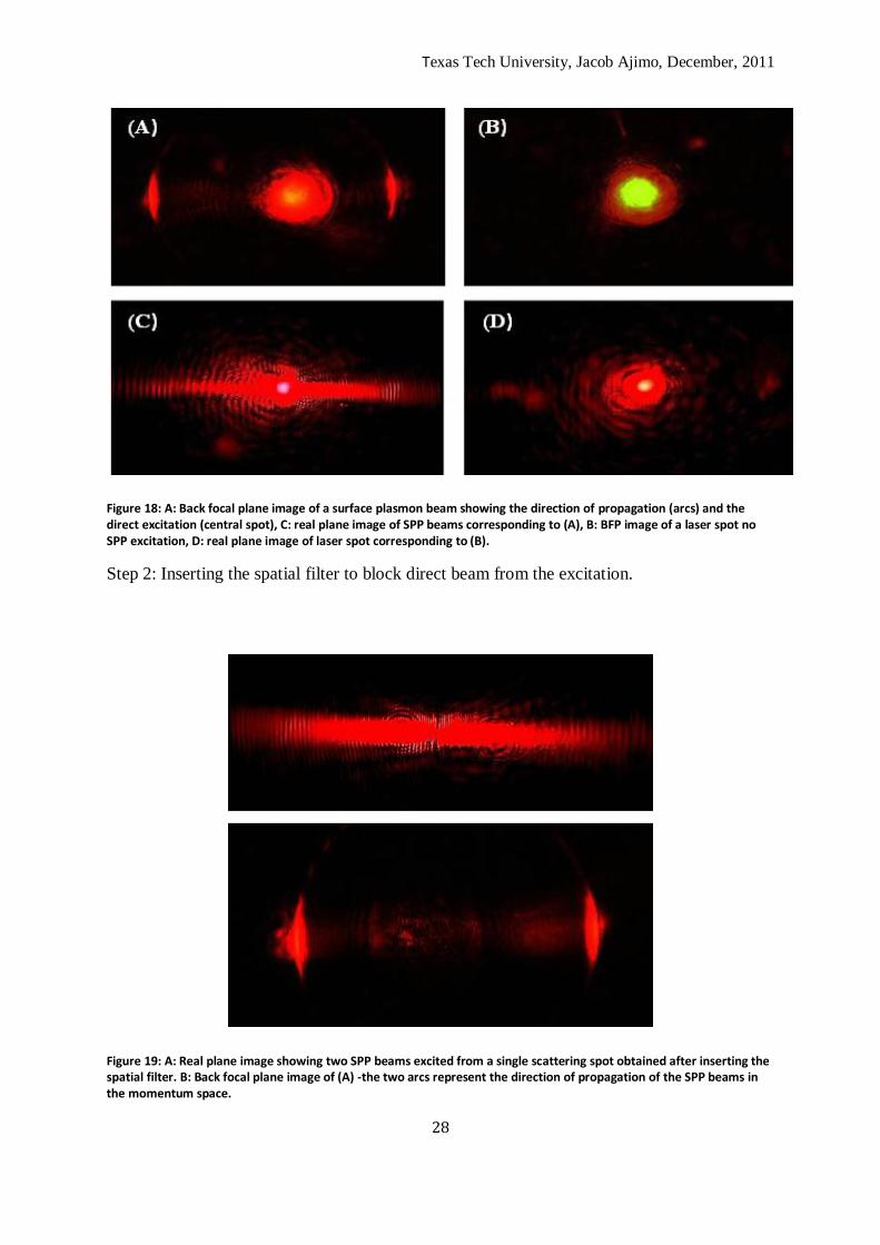
Step 2: Inserting the spatial filter to block direct beam from the excitation.
Figure 19: A: Real plane image showing two SPP beams excited from a single scattering spot obtained after inserting the spatial filter. B: Back focal plane image of (A) -the two arcs represent the direction of propagation of the SPP beams in the momentum space.
Texas Tech University, Jacob Ajimo, December, 2011
29
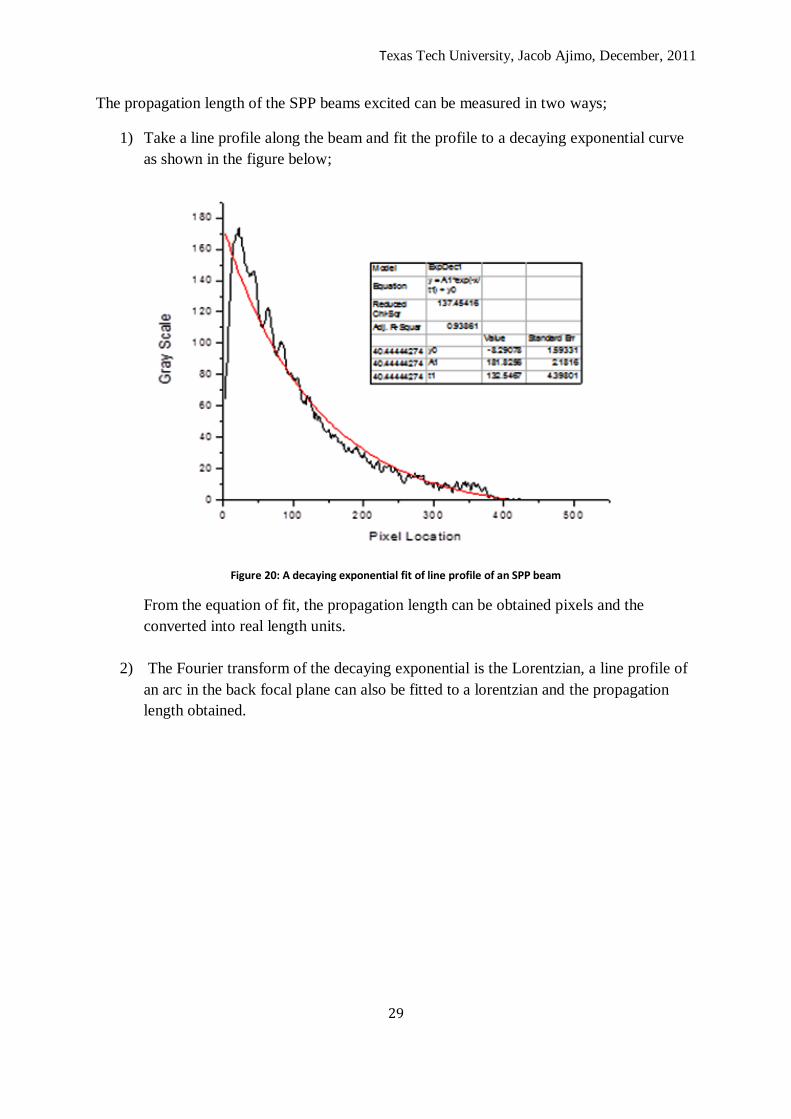
The propagation length of the SPP beams excited can be measured in two ways;
1) Take a line profile along the beam and fit the profile to a decaying exponential curve
as shown in the figure below;
Figure 20: A decaying exponential fit of line profile of an SPP beam
From the equation of fit, the propagation length can be obtained pixels and the
converted into real length units.
2) The Fourier transform of the decaying exponential is the Lorentzian, a line profile of
an arc in the back focal plane can also be fitted to a lorentzian and the propagation
length obtained.
Texas Tech University, Jacob Ajimo, December, 2011
30
Chapter Five
In this section, results from this work are presented. This includes both published and
unpublished results. Published results are presented as is with minor formatting and
numbering changes to ensure a complete readable text while preserving the intent.
Polarization states of surface plasmon polariton
Introduction
The term leakage microscopy (LM) refers to a group of recently developed microscopy
techniques (12-16) that rely on the collection of the light that leaks to the substrate during the
propagation of surface plasmon polaritons (SPP) modes (1). In the LM approach light is
collected by a high numerical aperture (NA) microscope objective lens, it provides raster free
images along with the capability of Fourier-plane imaging, it is relatively simple to
implement, and it is cost effective, particularly when compared with other methods such as
near-field scanning optical microscopy (17). Surface-emission and Fourier-plane images
obtained by LM have been used for characterization of SPP propagation in metal-dielectric
structures (14). Recently, SPP-coupled fluorescence (19)(21-22) combined with Fourier-
plane LM was used to investigate SPP stimulated emission in active plasmonic waveguides
(16). Although several works have been dedicated to the investigation of SPP propagation
using LM related techniques, no detailed investigation of the polarization states of guided
wave SPP modes using LM has been reported thus far. In this work, we demonstrate that the
polarization states of excited guided wave SPP modes can be unambiguously identified by
introducing a linear polarizer in the optical path of the light within a leakage-based
microscope. Using a Fourier-plane LM as a polarization characterization method, we
establish that in metal/dielectric/air slab waveguides with a thick dielectric layer the excited
SPP modes alternate between p- and s-polarization states. Furthermore, the Fourier-plane
images obtained by LM reveal that the intensity of the SPP-coupled fluorescence leaked to
the high NA microscope lens with a given polarization depends on the direction of
propagation of the excited SPP modes within the sample. In addition, we demonstrate the
application of Fourier-plane LM as a simple but effective method to identify the polarization
states of excited guided wave SPP in plasmonic waveguides.
Texas Tech University, Jacob Ajimo, December, 2011
31
Experimental setup and sample preparation
A schematic illustration of the leakage-based microscope used in this work is shown in Figure
21. Details of the microscope operation can be found in (15). Briefly, an inverted microscope
was modified to implement the proposed technique. The samples, coated with a fluorescent
material, are illuminated with a diode-pumped solid-state laser (λ=532 nm). Leakage of SPP-
coupled fluorescence is collected by a 100X immersion oil objective lens (NA=1.3). The
collimated back focal plane (BFP) emission from the objective is then transmitted through a
bandpass filter to block the direct beam from the laser. A linear polarizer is inserted after the
filter (Figure 21).
Figure 21. A schematic of the leakage-based microscope used for investigating polarization effects (10-11) (20).
A set of three lenses, internal to the microscope, perform magnification and aberration
corrections along with image formation. A CCD camera captures the image of the sample
surface after being partially reflected by the beam splitter. An external lens and a second
CCD camera collect the image formed in the back focal plane of the objective. The BFP
image corresponds to the Fourier-plane with respect to the sample surface-emission and thus
to a map of the two-dimensional momentum distribution of the SPP-coupled fluorescence
leaked into the substrate (12-16).

Texas Tech University, Jacob Ajimo, December, 2011
32
Figure 22: Schematic of cross-section of sample used in the study of polarization effects (12)
The structure of the first set of samples investigated in this work is illustrated in Figure 22.
The samples consist of a glass cover slip substrate, ~1 nm thick chromium adhesion layer,
followed by a 42 nm thick silver layer. A layer of 1–10% by weight poly (vinyl) alcohol
(PVA) doped with ~1 mM Rhodamine 6G (R6G), with emission maximum at wavelength
~566 nm, was spun on the top of the silver layer. The thickness of this layer was adjusted by
varying the concentration of the PVA material and typically ranged from 100 to 1000 nm. In
order to remove any solvent excess from the PVA layer, a post-baking step (1 min at 160 °C)
was performed on all samples. Following all measurements, the PVA-R6G layer can be
easily removed using alcohol and water rinsing. The second type of samples investigated by
LRM consisted of a periodic array of dielectric loaded SPP waveguides (DLSPPW) (16)(23).
Details of the sample fabrication can be found in (16). Briefly, the samples were fabricated
on a glass substrate which was covered with 50 nm thick gold layer. A ~1000 nm thick
PolyMethylMethAcrylate (PMMA) doped with R-6G was spin coated over the gold layer.
The doped PMMA layer was patterned using e-beam lithography. The arrays were fabricated
with 2 μm period and 1 μm waveguide width.
Experimental results and analysis
BFP images obtained using the leakage-based microscope with or without a linear polarizer
inserted after the bandpass filter, are shown in Figure 23. Without the polarizer (Figure 23(a)),
three distinct concentric rings were observed. The rings correspond to three different guided
wave SPP modes in the asymmetric metal/dielectric/air waveguide (15)(18).
Texas Tech University, Jacob Ajimo, December, 2011
33
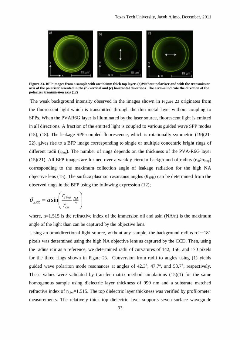
Figure 23. BFP images from a sample with an~990nm thick top layer. (a)Without polarizer and with the transmission
axis of the polarizer oriented in the (b) vertical and (c) horizontal directions. The arrows indicate the direction of the polarizer transmission axis (12)
The weak background intensity observed in the images shown in Figure 23 originates from
the fluorescent light which is transmitted through the thin metal layer without coupling to
SPPs. When the PVAR6G layer is illuminated by the laser source, fluorescent light is emitted
in all directions. A fraction of the emitted light is coupled to various guided wave SPP modes
(15), (18). The leakage SPP-coupled fluorescence, which is rotationally symmetric (19)(21-
22), gives rise to a BFP image corresponding to single or multiple concentric bright rings of
different radii (rring). The number of rings depends on the thickness of the PVA-R6G layer
(15)(21). All BFP images are formed over a weakly circular background of radius (rcir>rring)
corresponding to the maximum collection angle of leakage radiation for the high NA
objective lens (15). The surface plasmon resonance angles (θSPR) can be determined from the
observed rings in the BFP using the following expression (12);
nNA
cir
ring
SPRr
rasin
where, n=1.515 is the refractive index of the immersion oil and asin (NA/n) is the maximum
angle of the light than can be captured by the objective lens.
Using an omnidirectional light source, without any sample, the background radius rcir=181
pixels was determined using the high NA objective lens as captured by the CCD. Then, using
the radius rcir as a reference, we determined radii of curvatures of 142, 156, and 170 pixels
for the three rings shown in Figure 23. Conversion from radii to angles using (1) yields
guided wave polariton mode resonances at angles of 42.3°, 47.7°, and 53.7°, respectively.
These values were validated by transfer matrix method simulations (15)(1) for the same
homogenous sample using dielectric layer thickness of 990 nm and a substrate matched
refractive index of ndiel=1.515. The top dielectric layer thickness was verified by profilometer
measurements. The relatively thick top dielectric layer supports seven surface waveguide

Texas Tech University, Jacob Ajimo, December, 2011
34
plasmon related resonances. This was also verified experimentally by performing angular-
emission measurements of the same sample using a hemi cylindrical prism configuration (19)
yielding 7 emission peaks. Excellent agreement between simulated and determined SPR
angles was obtained for the first three SPR angles corresponding to the rings shown in Figure
23. The remaining four angular resonances occur at angles that are above the maximum
acceptance angle (~59°) of the high NA objective, and could not be collected by the lens.
The insertion of a linear polarizer after the bandpass filter allows us to study the state of
polarization of the SPP-coupled fluorescence leaked to the sample substrate that was
collected by the high NA microscope objective. As shown in Figure 23(b) and (c), the
polarizer was oriented parallel to the BFP with transmission axis indicated by the double
arrows (horizontal or vertical). For a given ring at the BFP, the polarization of the leakage
radiation depends on the direction of propagation and polarization of the guided wave SPP
modes in the sample. With the insertion of the polarizer, the BFP images are modified from
continuous rings (Figure 23(a)) to pairs of arcs symmetrically located (horizontal or vertical)
with respect to the center of the original rings. For a given direction in the BFP image, the
most internal and external rings have the same polarization which is the opposite of that of
the ring between them. Figure 24 illustrates the relation between the polarization states of the
leakage radiation in the BFP and the guided wave SPP modes in the sample.
Texas Tech University, Jacob Ajimo, December, 2011
35
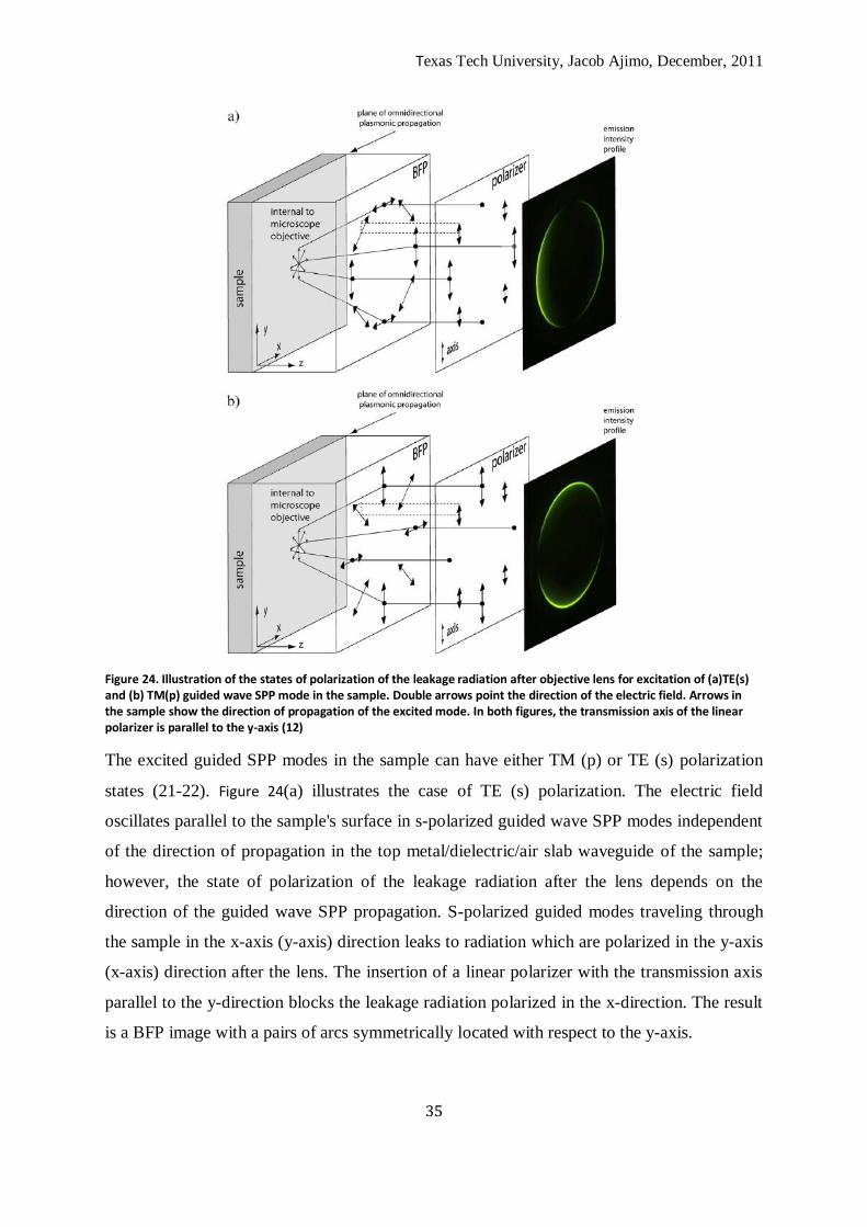
Figure 24. Illustration of the states of polarization of the leakage radiation after objective lens for excitation of (a)TE(s) and (b) TM(p) guided wave SPP mode in the sample. Double arrows point the direction of the electric field. Arrows in the sample show the direction of propagation of the excited mode. In both figures, the transmission axis of the linear polarizer is parallel to the y-axis (12)
The excited guided SPP modes in the sample can have either TM (p) or TE (s) polarization
states (21-22). Figure 24(a) illustrates the case of TE (s) polarization. The electric field
oscillates parallel to the sample's surface in s-polarized guided wave SPP modes independent
of the direction of propagation in the top metal/dielectric/air slab waveguide of the sample;
however, the state of polarization of the leakage radiation after the lens depends on the
direction of the guided wave SPP propagation. S-polarized guided modes traveling through
the sample in the x-axis (y-axis) direction leaks to radiation which are polarized in the y-axis
(x-axis) direction after the lens. The insertion of a linear polarizer with the transmission axis
parallel to the y-direction blocks the leakage radiation polarized in the x-direction. The result
is a BFP image with a pairs of arcs symmetrically located with respect to the y-axis.
Texas Tech University, Jacob Ajimo, December, 2011
36
In contrast, for p-polarized guided SPP modes Figure 24(b), the electric field oscillates
perpendicularly to the sample's surface. P-polarized modes traveling in the x-axis (y-axis)
direction leak to radiation which is polarized in the x-axis (y-axis) direction after the lens.
The insertion of a linear polarizer with the transmission axis parallel to the y-direction blocks
the leakage radiation polarized in the x-direction, resulting in a BFP image with a pairs of
arcs symmetrically located with respect to the x-axis. The coordinate system shown in figure
19 will be used to study the polarization effects on all images discussed in this work. In order
to simplify image analysis, horizontal (vertical) direction will be also used to describe the x-
axis (y-axis) directions. A comparison between Figure 23 and Figure 24 permits us to identify
alternating p- and s-polarizations of the guided wave SPP modes excited in the asymmetric
metal/dielectric/air slab waveguide of the sample. Guided wave SPP modes with p-
polarization leak into the most internal and external rings while an s-polarized mode leaks to
the ring in between. The BFP image shown in Figure 23(b) was obtained by positioning the
polarizer transmission axis in the vertical direction. In this case, p-polarized modes traversing
the sample surface in the y-direction couple to the free propagation light with vertical
polarization, which passes through the polarizer, and results in the pairs of bright arcs,
observed intersecting the y-axis in Figure 23(b). However, p-polarized modes traversing the
sample surface in the x-direction couple to the free propagation light with horizontal
polarization. This results in the elimination of the most internal and external rings in the x-
direction. In contrast, a guided wave SPP mode with s-polarization leaks to the central ring.
When traversing in the x-direction, it couples to the free propagation light with vertical
polarization, which passes through the polarizer, and results in the bright arcs observed
intersecting the x-axis shown in Figure 23(b). Likewise, the BFP image shown in figure 18(c)
can be explained in a similar manner, but orienting the polarizer transmission axis in the
horizontal direction. The results shown in Figure 23 suggest that the polarization state of an
excited guided wave SPP mode can be identified using a simple rule: if the introduction of a
linear polarizer in the optical path within the microscope results in BFP intensity decrease in
the direction of the polarizer's transmission axis, the excited SPP mode has TE (s)
polarization. If the BFP intensity decrease occurs in the direction perpendicular to the
transmission axis of the polarizer, the excited SPP mode has TM (p) polarization.
In order to demonstrate the application of the polarization rules to plasmonic structures, we
investigated the polarization states of excited modes in the array of DLSPPW.
Texas Tech University, Jacob Ajimo, December, 2011
37
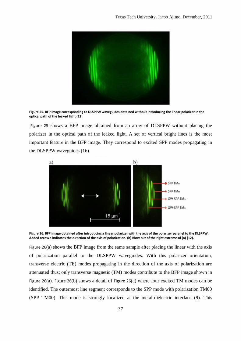
Figure 25. BFP image corresponding to DLSPPW waveguides obtained without introducing the linear polarizer in the optical path of the leaked light (12)
Figure 25 shows a BFP image obtained from an array of DLSPPW without placing the
polarizer in the optical path of the leaked light. A set of vertical bright lines is the most
important feature in the BFP image. They correspond to excited SPP modes propagating in
the DLSPPW waveguides (16).
Figure 26. BFP image obtained after introducing a linear polarizer with the axis of the polarizer parallel to the DLSPPW. Added arrow s indicates the direction of the axis of polarization. (b) Blow out of the right extreme of (a) (12).
Figure 26(a) shows the BFP image from the same sample after placing the linear with the axis
of polarization parallel to the DLSPPW waveguides. With this polarizer orientation,
transverse electric (TE) modes propagating in the direction of the axis of polarization are
attenuated thus; only transverse magnetic (TM) modes contribute to the BFP image shown in
Figure 26(a). Figure 26(b) shows a detail of Figure 26(a) where four excited TM modes can be
identified. The outermost line segment corresponds to the SPP mode with polarization TM00
(SPP TM00). This mode is strongly localized at the metal-dielectric interface (9). This
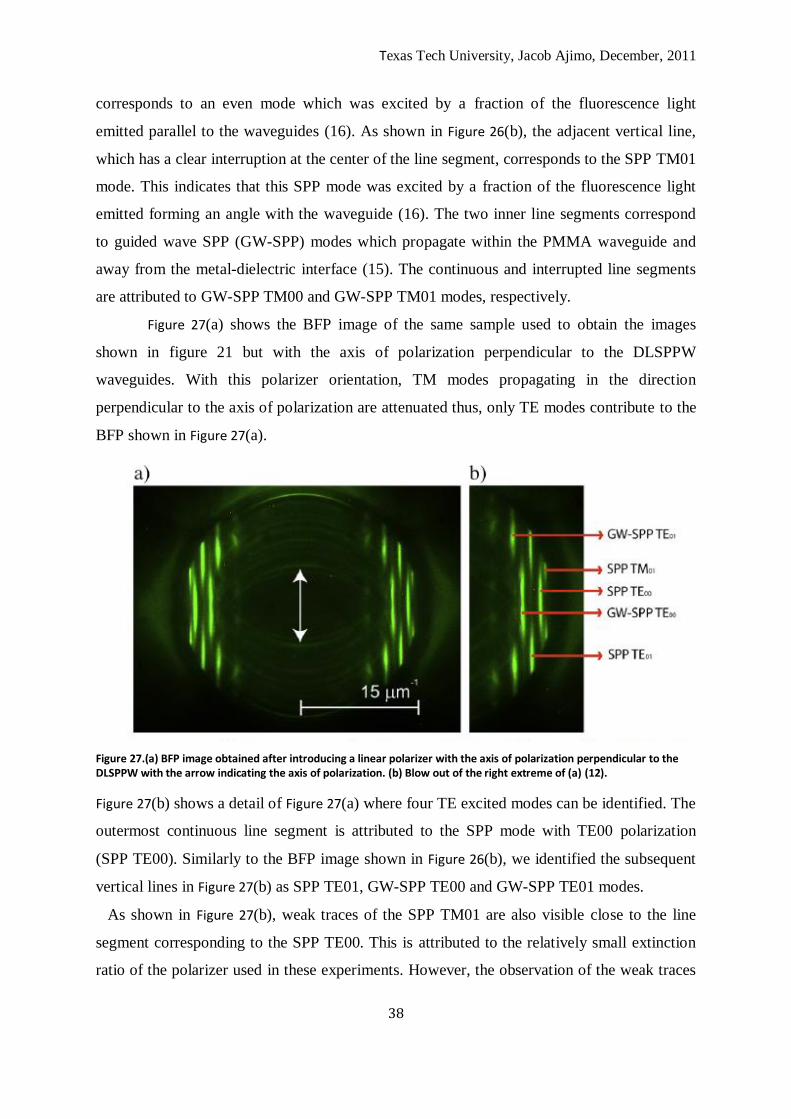
Texas Tech University, Jacob Ajimo, December, 2011
38
corresponds to an even mode which was excited by a fraction of the fluorescence light
emitted parallel to the waveguides (16). As shown in Figure 26(b), the adjacent vertical line,
which has a clear interruption at the center of the line segment, corresponds to the SPP TM01
mode. This indicates that this SPP mode was excited by a fraction of the fluorescence light
emitted forming an angle with the waveguide (16). The two inner line segments correspond
to guided wave SPP (GW-SPP) modes which propagate within the PMMA waveguide and
away from the metal-dielectric interface (15). The continuous and interrupted line segments
are attributed to GW-SPP TM00 and GW-SPP TM01 modes, respectively.
Figure 27(a) shows the BFP image of the same sample used to obtain the images
shown in figure 21 but with the axis of polarization perpendicular to the DLSPPW
waveguides. With this polarizer orientation, TM modes propagating in the direction
perpendicular to the axis of polarization are attenuated thus, only TE modes contribute to the
BFP shown in Figure 27(a).
Figure 27.(a) BFP image obtained after introducing a linear polarizer with the axis of polarization perpendicular to the DLSPPW with the arrow indicating the axis of polarization. (b) Blow out of the right extreme of (a) (12).
Figure 27(b) shows a detail of Figure 27(a) where four TE excited modes can be identified. The
outermost continuous line segment is attributed to the SPP mode with TE00 polarization
(SPP TE00). Similarly to the BFP image shown in Figure 26(b), we identified the subsequent
vertical lines in Figure 27(b) as SPP TE01, GW-SPP TE00 and GW-SPP TE01 modes.
As shown in Figure 27(b), weak traces of the SPP TM01 are also visible close to the line
segment corresponding to the SPP TE00. This is attributed to the relatively small extinction
ratio of the polarizer used in these experiments. However, the observation of the weak traces
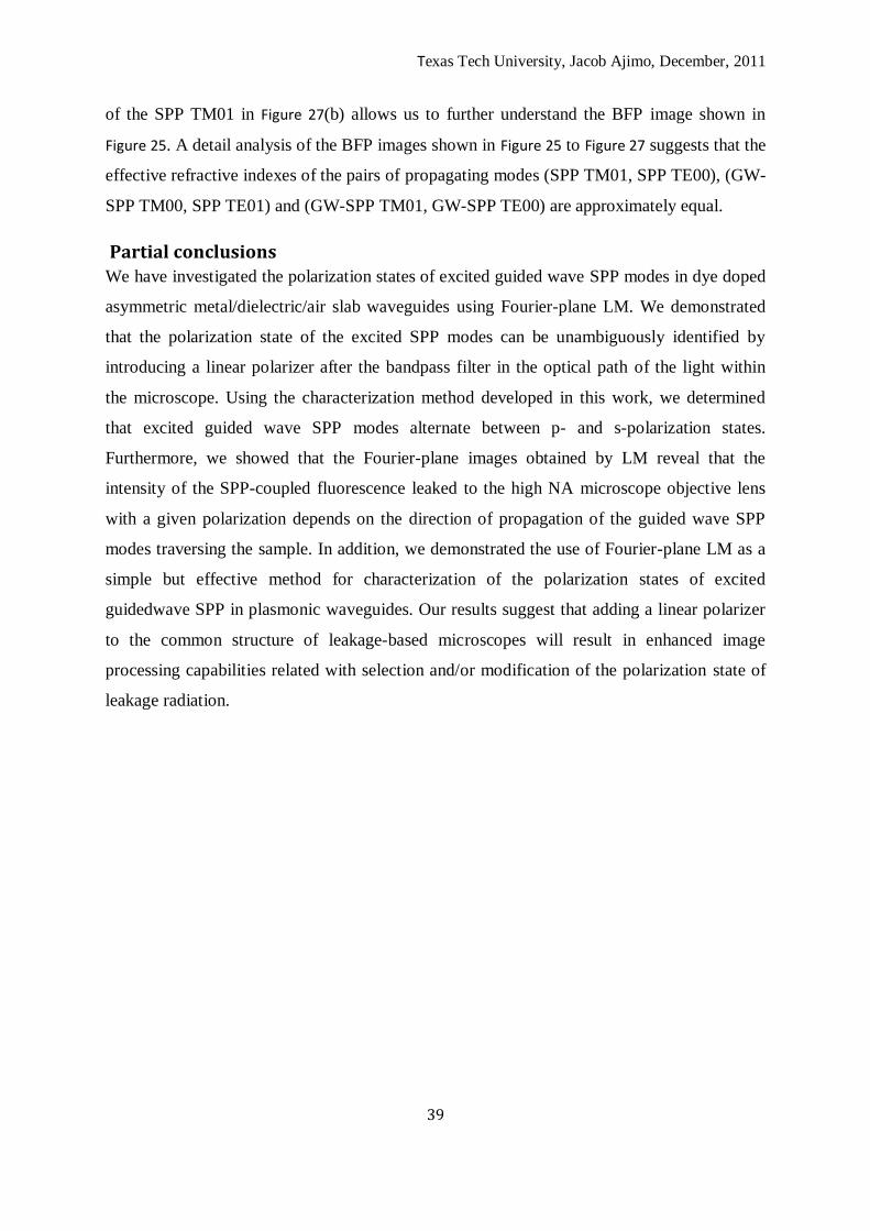
Texas Tech University, Jacob Ajimo, December, 2011
39
of the SPP TM01 in Figure 27(b) allows us to further understand the BFP image shown in
Figure 25. A detail analysis of the BFP images shown in Figure 25 to Figure 27 suggests that the
effective refractive indexes of the pairs of propagating modes (SPP TM01, SPP TE00), (GW-
SPP TM00, SPP TE01) and (GW-SPP TM01, GW-SPP TE00) are approximately equal.
Partial conclusions
We have investigated the polarization states of excited guided wave SPP modes in dye doped
asymmetric metal/dielectric/air slab waveguides using Fourier-plane LM. We demonstrated
that the polarization state of the excited SPP modes can be unambiguously identified by
introducing a linear polarizer after the bandpass filter in the optical path of the light within
the microscope. Using the characterization method developed in this work, we determined
that excited guided wave SPP modes alternate between p- and s-polarization states.
Furthermore, we showed that the Fourier-plane images obtained by LM reveal that the
intensity of the SPP-coupled fluorescence leaked to the high NA microscope objective lens
with a given polarization depends on the direction of propagation of the guided wave SPP
modes traversing the sample. In addition, we demonstrated the use of Fourier-plane LM as a
simple but effective method for characterization of the polarization states of excited
guidedwave SPP in plasmonic waveguides. Our results suggest that adding a linear polarizer
to the common structure of leakage-based microscopes will result in enhanced image
processing capabilities related with selection and/or modification of the polarization state of
leakage radiation.
Texas Tech University, Jacob Ajimo, December, 2011
40
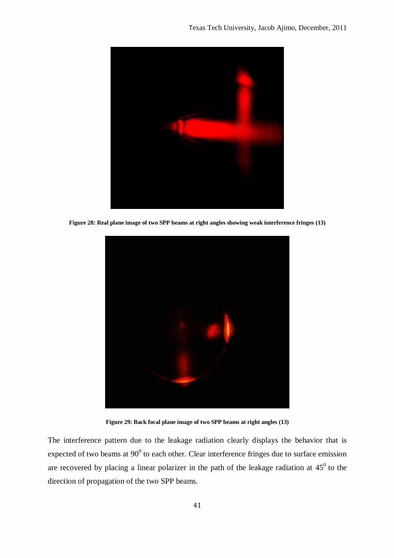
Interference due to perpendicular SPP beams and consequences
Two lines forming an L pattern, each of length 25m with a cross section as shown in Figure
16 were used as samples for this experiment. Two beams from HeNe laser (632.8nm)
were focused at two spots on each arm of the pattern to excite SPP beams at the gold-air
interface using the low NA objective (40X, NA=0.65) as shown in the experimental set-up.
The leakage radiation from the SPP beam is therefore collected by the high NA oil immersion
objective (100X, NA=1.3) and transmitted through the internal lenses of the microscope. A
spatial filter was placed just after the high NA objective to block direct beam from the laser.
The location of the spatial filter is the BFP making it suitable for efficient identification of the
direct excitation as can be seen from the BFP of the CCD camera. The resulting beam due to
the leakage of radiation was then allowed to enter the internal lenses of the microscope and
detected by the CCD camera both at the real plane and the BFP. Details on the image
formation of the microscope have been discussed elsewhere (16-17). The real plane image
and BFP image obtained are shown in Figure 28 and Figure 29 respectively. Since the two
SPP beams on the sample surface are of identical polarization(TM), we expected clear
interference fringes in the real plane image Figure 28. However, the interference fringes in
Figure 28 are not so clear and so is the BFP image Figure 29. It was therefore unclear whether
the real plane and the BFP images were a reliable representation of the SPP beam behavior. A
linear polarizer was then placed on the optical path of the leakage radiation after the spatial
filter to improve the signal to noise of the image formed. The resulting images are shown in
Figure 30 and Figure 31.
Texas Tech University, Jacob Ajimo, December, 2011
41
Figure 28: Real plane image of two SPP beams at right angles showing weak interference fringes (13)
Figure 29: Back focal plane image of two SPP beams at right angles (13)
The interference pattern due to the leakage radiation clearly displays the behavior that is
expected of two beams at 900 to each other. Clear interference fringes due to surface emission
are recovered by placing a linear polarizer in the path of the leakage radiation at 450
to the
direction of propagation of the two SPP beams.
Texas Tech University, Jacob Ajimo, December, 2011
42
Figure 30: Real plane image of two SPP beams at right angles showing clear interference fringes (13)
Figure 31: Back focal plane image of two SPP beams at right angles showing clear arcs (13)
The polarization state of leakage radiation through the substrate depends on the direction of
propagation of the SPP beams on the sample surface. Two SPP beams at right angles
therefore result into leakage radiation of different polarization. This accounts for the blurry
Kx
Texas Tech University, Jacob Ajimo, December, 2011
43
nature of the interference fringes in Figure 28 and the absence of well defined arcs in Figure
29. When the polarizer is placed at 450 to both beams, beams of the same polarization are
allowed to pass through. This explains the appearance of clear interference fringes in the
images in Figure 30 and well defined arcs in Figure 31. The effects of the polarization state of
SPP modes on the image formation were reported in a recent study (11). Results of this
previous study provided the basis for the use of linear polarizer to identify the different
polarization states and improve the signal to noise ratio.
The experiment clearly demonstrates the dependence of interference fringe formation on the
polarization state of the leakage radiation. This property is best described by a quantum
eraser. The implementation of SPP quantum eraser was displayed in the experiment. Details
of this result are published (7-8) and will be described in detail later in this chapter.
The formation of clear interference fringes and the subsequent arcs in the back focal image is
a stack reminder of the photon propagation paradox. Main questions being “how do photons
propagate?” and that if the photons travelled in the region where the interference pattern was
formed, how were they detectable? These are some interesting questions elicited by these
results and open for further investigation. This work does not attempt to do this.
Texas Tech University, Jacob Ajimo, December, 2011
44
Parallel SPP beam propagation
Introduction Double and multiple-slit experiments with light have been widely studied (24-31). Young's
double-slit experiment is described in the majority of modern general physics books (24-27)
its simplicity provides convincing evidence of the wave nature of light. The same experiment
but using feeble light is commonly included in textbooks for illustrating the corpuscular
nature of light. Interference between ultra fast pulses of light which do not overlap and
occurrence of interference in conditions where the which-path information is available has
been demonstrated using a multiple-slit arrangement. In all these experiments, the double or
multiple-slit arrangements are often illuminated by a collimated beam. Each slit is delimited
by the interface between two media, i.e., by the slit's walls. Diffraction of light at each slit
spreads out the light passing through it. This results in superposition and interference between
light diffracted by each slit. As a consequence, the diffraction–interference pattern produced
by a multiple-slit arrangement is often described by the product of two factors; the diffraction
pattern factor describing the envelope of the pattern and the “pure” interference contribution
factor. In this work, we revisit the double-slit experiment by studying the contribution of the
slits' walls to the observed interference pattern. To do this, we used surface plasmon polariton
(SPP) tomography techniques to implement a double-slit without walls. SPP tomography (12-
15) (32) is an effective far-field optical technique for imaging the two-dimensional
propagation of SPPs (1-2) along a metal–dielectric interface. In SPP tomography, the images
are formed as a result of the collection of the light that leaks through the metal– dielectric
interface. When a collimated SPP beam propagates along the uniform metal–air interface of a
sample, light leaks from every point of the sample surface where the SPP beam passes
through. In Figure 32, the relative direction of the leakage radiation with respect to the SPP
beam is illustrated. The leaked light forms a characteristic angle θSPP in a plane perpendicular
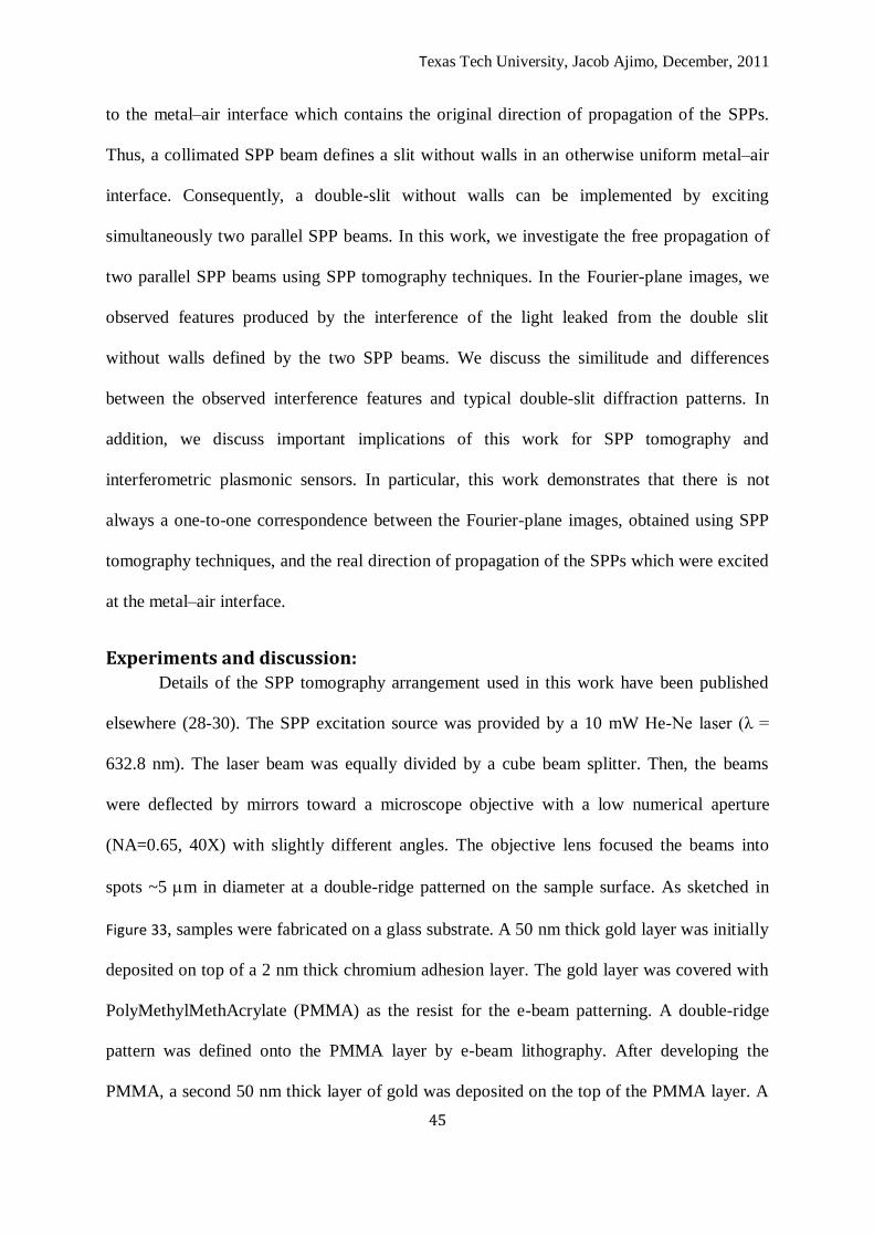
Texas Tech University, Jacob Ajimo, December, 2011
45
to the metal–air interface which contains the original direction of propagation of the SPPs.
Thus, a collimated SPP beam defines a slit without walls in an otherwise uniform metal–air
interface. Consequently, a double-slit without walls can be implemented by exciting
simultaneously two parallel SPP beams. In this work, we investigate the free propagation of
two parallel SPP beams using SPP tomography techniques. In the Fourier-plane images, we
observed features produced by the interference of the light leaked from the double slit
without walls defined by the two SPP beams. We discuss the similitude and differences
between the observed interference features and typical double-slit diffraction patterns. In
addition, we discuss important implications of this work for SPP tomography and
interferometric plasmonic sensors. In particular, this work demonstrates that there is not
always a one-to-one correspondence between the Fourier-plane images, obtained using SPP
tomography techniques, and the real direction of propagation of the SPPs which were excited
at the metal–air interface.
Experiments and discussion:
Details of the SPP tomography arrangement used in this work have been published
elsewhere (28-30). The SPP excitation source was provided by a 10 mW He-Ne laser (λ =
632.8 nm). The laser beam was equally divided by a cube beam splitter. Then, the beams
were deflected by mirrors toward a microscope objective with a low numerical aperture
(NA=0.65, 40X) with slightly different angles. The objective lens focused the beams into
spots ~5 m in diameter at a double-ridge patterned on the sample surface. As sketched in
Figure 33, samples were fabricated on a glass substrate. A 50 nm thick gold layer was initially
deposited on top of a 2 nm thick chromium adhesion layer. The gold layer was covered with
PolyMethylMethAcrylate (PMMA) as the resist for the e-beam patterning. A double-ridge
pattern was defined onto the PMMA layer by e-beam lithography. After developing the
PMMA, a second 50 nm thick layer of gold was deposited on the top of the PMMA layer. A
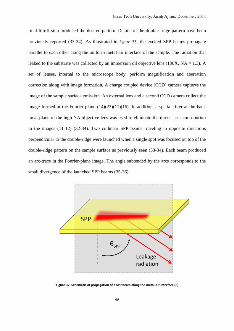
Texas Tech University, Jacob Ajimo, December, 2011
46
final liftoff step produced the desired pattern. Details of the double-ridge pattern have been
previously reported (33-34). As illustrated in Figure 33, the excited SPP beams propagate
parallel to each other along the uniform metal-air interface of the sample. The radiation that
leaked to the substrate was collected by an immersion oil objective lens (100X, NA = 1.3). A
set of lenses, internal to the microscope body, perform magnification and aberration
correction along with image formation. A charge coupled device (CCD) camera captures the
image of the sample surface emission. An external lens and a second CCD camera collect the
image formed at the Fourier plane (14)(23)(11)(16). In addition, a spatial filter at the back
focal plane of the high NA objective lens was used to eliminate the direct laser contribution
to the images (11-12) (32-34). Two collinear SPP beams traveling in opposite directions
perpendicular to the double-ridge were launched when a single spot was focused on top of the
double-ridge pattern on the sample surface as previously seen (33-34). Each beam produced
an arc-trace in the Fourier-plane image. The angle subtended by the arcs corresponds to the
small divergence of the launched SPP beams (35-36).
Figure 32: Schematic of propagation of a SPP beam along the metal-air interface (8)
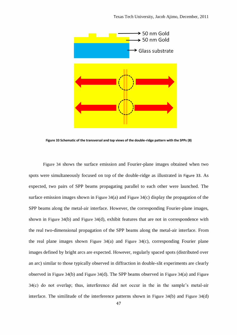
Texas Tech University, Jacob Ajimo, December, 2011
47
Figure 33 Schematic of the transversal and top views of the double-ridge pattern with the SPPs (8)
Figure 34 shows the surface emission and Fourier-plane images obtained when two
spots were simultaneously focused on top of the double-ridge as illustrated in Figure 33. As
expected, two pairs of SPP beams propagating parallel to each other were launched. The
surface emission images shown in Figure 34(a) and Figure 34(c) display the propagation of the
SPP beams along the metal-air interface. However, the corresponding Fourier-plane images,
shown in Figure 34(b) and Figure 34(d), exhibit features that are not in correspondence with
the real two-dimensional propagation of the SPP beams along the metal-air interface. From
the real plane images shown Figure 34(a) and Figure 34(c), corresponding Fourier plane
images defined by bright arcs are expected. However, regularly spaced spots (distributed over
an arc) similar to those typically observed in diffraction in double-slit experiments are clearly
observed in Figure 34(b) and Figure 34(d). The SPP beams observed in Figure 34(a) and Figure
34(c) do not overlap; thus, interference did not occur in the in the sample’s metal-air
interface. The similitude of the interference patterns shown in Figure 34(b) and Figure 34(d)
Texas Tech University, Jacob Ajimo, December, 2011
48
with typical double-slit diffraction experiments can be verified by comparing Figure 34(a) and
Figure 34(b) with Figure 34(c) and Figure 34(d). When the separation between the two parallel
SPP beams at the sample surface is increases from 5.6m to 9.3m, the separation between
the interference spots in the Fourier-plane images decreases. This is a well-known
characteristic of multiple-slit diffraction patterns. Thus, the features observed in these
Fourier-plane images are due to the interference of the leaked light from the two parallel SPP
beams. This result demonstrates that the Fourier-plane images obtained using SPP
tomography techniques should be interpreted with caution (37)(38). There is no one-to-one
correspondence between the Fourier-plane images shown in Figure 34(b) and Figure 34(d) and
the momentum distribution corresponding to two SPPs beams propagating in the same
direction along the metal-air interface. The real distribution of SPP propagation directions at
the metal-air interface includes all angles subtended by the arc containing all the interference
spots. This also includes the angles corresponding to the interference minima between the
bright spots observed in the Fourier-plane images. SPP tomography is not a direct imaging
technique. Thus, it is crucial for a correct interpretation of the images, to account for the
effects of the free propagation of the leaked light on the imaging process.
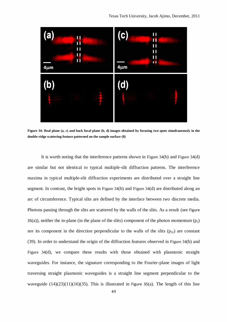
Texas Tech University, Jacob Ajimo, December, 2011
49
Figure 34: Real plane (a, c) and back focal plane (b, d) images obtained by focusing two spots simultaneously in the
double-ridge scattering feature patterned on the sample surface (8)
It is worth noting that the interference patterns shown in Figure 34(b) and Figure 34(d)
are similar but not identical to typical multiple-slit diffraction patterns. The interference
maxima in typical multiple-slit diffraction experiments are distributed over a straight line
segment. In contrast, the bright spots in Figure 34(b) and Figure 34(d) are distributed along an
arc of circumference. Typical slits are defined by the interface between two discrete media.
Photons passing through the slits are scattered by the walls of the slits. As a result (see Figure
35(a)), neither the in-plane (in the plane of the slits) component of the photon momentum (p ||)
nor its component in the direction perpendicular to the walls of the slits (p ||x) are constant
(39). In order to understand the origin of the diffraction features observed in Figure 34(b) and
Figure 34(d), we compare these results with those obtained with plasmonic straight
waveguides. For instance, the signature corresponding to the Fourier-plane images of light
traversing straight plasmonic waveguides is a straight line segment perpendicular to the
waveguide (14)(23)(11)(16)(35). This is illustrated in Figure 35(a). The length of this line
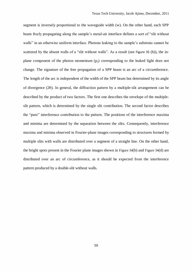
Texas Tech University, Jacob Ajimo, December, 2011
50
segment is inversely proportional to the waveguide width (w). On the other hand, each SPP
beam freely propagating along the sample’s metal-air interface defines a sort of “slit without
walls” in an otherwise uniform interface. Photons leaking to the sample’s substrate cannot be
scattered by the absent walls of a “slit without walls”. As a result (see Figure 35 (b)), the in-
plane component of the photon momentum (p ||) corresponding to the leaked light does not
change. The signature of the free propagation of a SPP beam is an arc of a circumference.
The length of the arc is independent of the width of the SPP beam but determined by its angle
of divergence (2). In general, the diffraction pattern by a multiple-slit arrangement can be
described by the product of two factors. The first one describes the envelope of the multiple-
slit pattern, which is determined by the single slit contribution. The second factor describes
the “pure” interference contribution to the pattern. The positions of the interference maxima
and minima are determined by the separation between the slits. Consequently, interference
maxima and minima observed in Fourier-plane images corresponding to structures formed by
multiple slits with walls are distributed over a segment of a straight line. On the other hand,
the bright spots present in the Fourier plane images shown in Figure 34(b) and Figure 34(d) are
distributed over an arc of circumference, as it should be expected from the interference
pattern produced by a double-slit without walls.
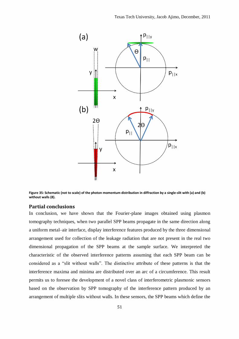
Texas Tech University, Jacob Ajimo, December, 2011
51
Figure 35: Schematic (not to scale) of the photon momentum distribution in diffraction by a single-slit with (a) and (b) without walls (8).
Partial conclusions In conclusion, we have shown that the Fourier-plane images obtained using plasmon
tomography techniques, when two parallel SPP beams propagate in the same direction along
a uniform metal–air interface, display interference features produced by the three dimensional
arrangement used for collection of the leakage radiation that are not present in the real two
dimensional propagation of the SPP beams at the sample surface. We interpreted the
characteristic of the observed interference patterns assuming that each SPP beam can be
considered as a “slit without walls”. The distinctive attribute of these patterns is that the
interference maxima and minima are distributed over an arc of a circumference. This result
permits us to foresee the development of a novel class of interferometric plasmonic sensors
based on the observation by SPP tomography of the interference pattern produced by an
arrangement of multiple slits without walls. In these sensors, the SPP beams which define the

Texas Tech University, Jacob Ajimo, December, 2011
52
slits without walls travel through the metal–dielectric interface resulting in an interference
pattern that is very sensitive to relative changes in the optical paths. Moreover, the multiple-
slit without walls can be easily reconfigured by manipulating SPP beams in real time.
Texas Tech University, Jacob Ajimo, December, 2011
53
Double slit diffraction of two-dimensional light using plasmon
tomography
Introduction A surface plasmon polariton (SPP) is an electromagnetic wave coupled to collective
oscillations of free electrons which is confined at the interface between a metal and a
dielectric (1). The inherent confinement of SPP to the metal-dielectric interface has motivated
numerous SPP applications based on their sub-wavelength capabilities (40-42). In addition,
the intrinsic quasi two-dimensional (2D) nature of SPPs has motivated fundamental studies in
2D light propagation, interference, and diffraction phenomena (43) (32-34) which are highly
needed for design and simulation of SPP-based devices. Young’s double slit experiment is a
critical step in the understanding of combined diffraction and interference phenomena
(24)(6). Diffraction of SPP by a double slit has already been studied using optical near-field
techniques (1). However, due to the inherent close proximity between the optical probe and
the surface under study, near-field techniques may distort the actual electric field distribution
in the sample. Thus, alternative non-disturbing techniques are needed to investigate SPP
diffraction by a double slit. A possible solution to this issue is the use of optical far-field
techniques such as SPP tomography (32) to obtain the detailed information about electric
field distribution within SPP structures.
SPP tomography is a non-disturbing optical far-field technique that does not involve
raster scanning, and permits simple imaging of SPP propagation, interference, and diffraction
phenomena. To the best of the authors’ knowledge, we report for the first time, non-
disturbing observation of SPP diffraction by a double slit using SPP tomography technique.
We present a detailed discussion of the obtained surface emission (SE) and Fourier-plane
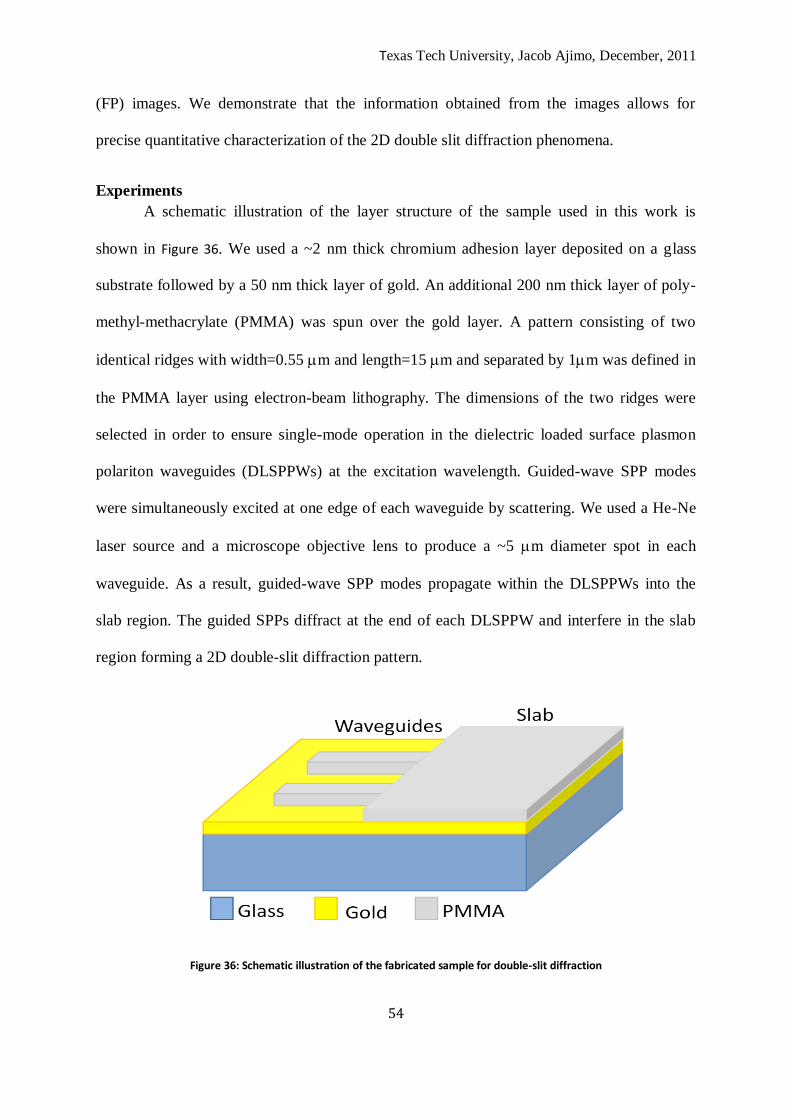
Texas Tech University, Jacob Ajimo, December, 2011
54
(FP) images. We demonstrate that the information obtained from the images allows for
precise quantitative characterization of the 2D double slit diffraction phenomena.
Experiments
A schematic illustration of the layer structure of the sample used in this work is
shown in Figure 36. We used a ~2 nm thick chromium adhesion layer deposited on a glass
substrate followed by a 50 nm thick layer of gold. An additional 200 nm thick layer of poly-
methyl-methacrylate (PMMA) was spun over the gold layer. A pattern consisting of two
identical ridges with width=0.55 m and length=15m and separated by 1m was defined in
the PMMA layer using electron-beam lithography. The dimensions of the two ridges were
selected in order to ensure single-mode operation in the dielectric loaded surface plasmon
polariton waveguides (DLSPPWs) at the excitation wavelength. Guided-wave SPP modes
were simultaneously excited at one edge of each waveguide by scattering. We used a He-Ne
laser source and a microscope objective lens to produce a ~5 m diameter spot in each
waveguide. As a result, guided-wave SPP modes propagate within the DLSPPWs into the
slab region. The guided SPPs diffract at the end of each DLSPPW and interfere in the slab
region forming a 2D double-slit diffraction pattern.
Figure 36: Schematic illustration of the fabricated sample for double-slit diffraction
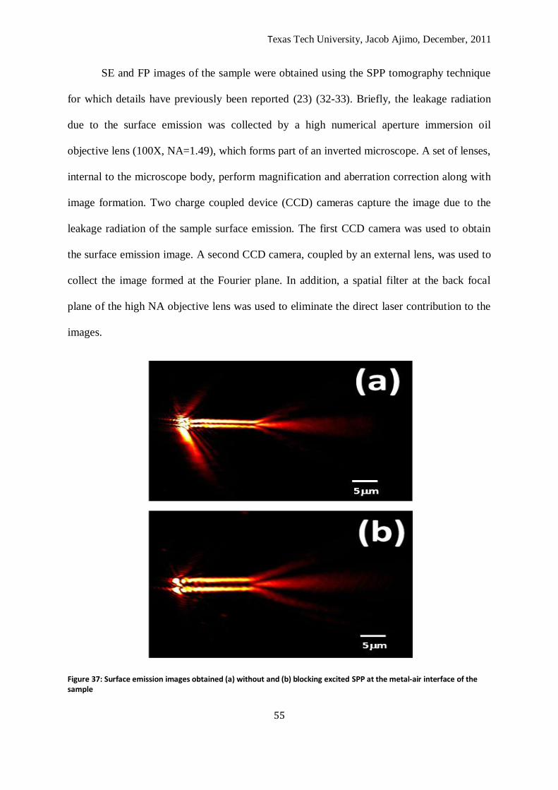
Texas Tech University, Jacob Ajimo, December, 2011
55
SE and FP images of the sample were obtained using the SPP tomography technique
for which details have previously been reported (23) (32-33). Briefly, the leakage radiation
due to the surface emission was collected by a high numerical aperture immersion oil
objective lens (100X, NA=1.49), which forms part of an inverted microscope. A set of lenses,
internal to the microscope body, perform magnification and aberration correction along with
image formation. Two charge coupled device (CCD) cameras capture the image due to the
leakage radiation of the sample surface emission. The first CCD camera was used to obtain
the surface emission image. A second CCD camera, coupled by an external lens, was used to
collect the image formed at the Fourier plane. In addition, a spatial filter at the back focal
plane of the high NA objective lens was used to eliminate the direct laser contribution to the
images.
Figure 37: Surface emission images obtained (a) without and (b) blocking excited SPP at the metal-air interface of the sample
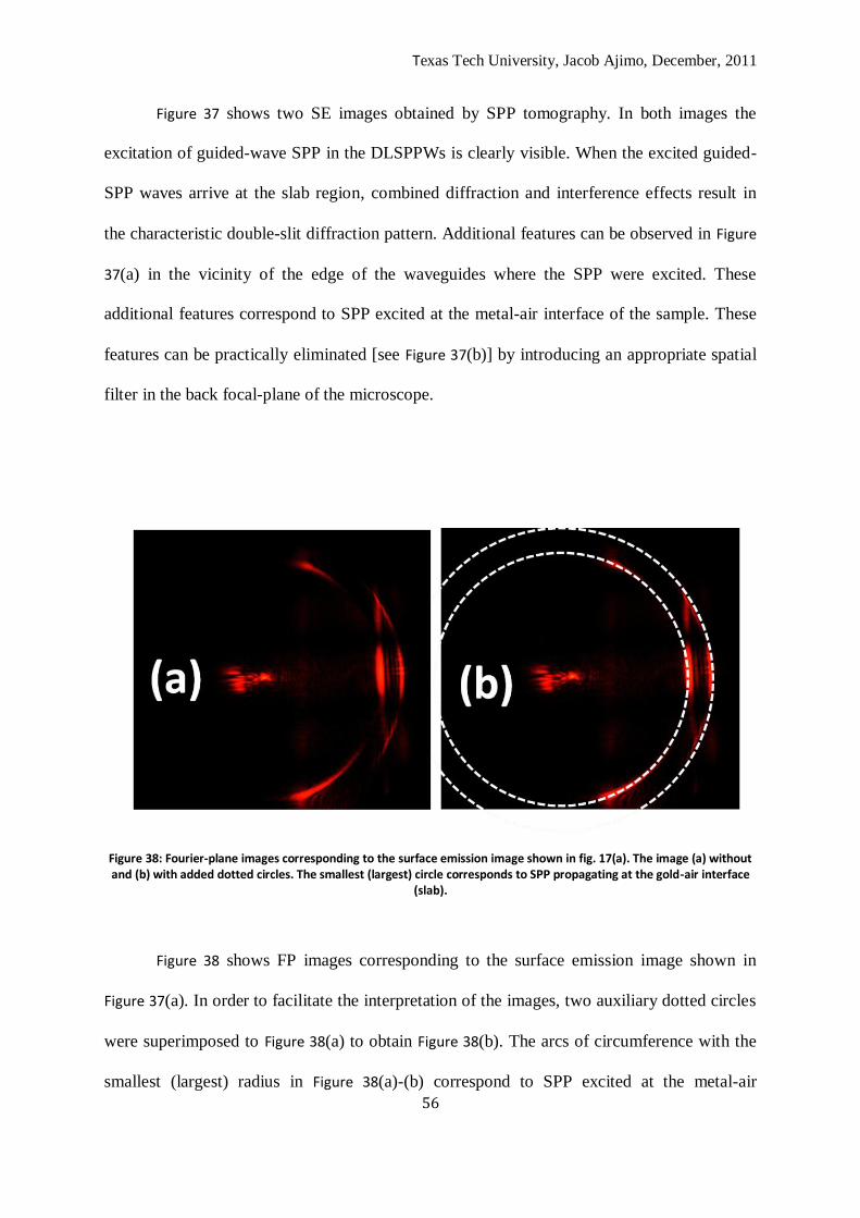
Texas Tech University, Jacob Ajimo, December, 2011
56
Figure 37 shows two SE images obtained by SPP tomography. In both images the
excitation of guided-wave SPP in the DLSPPWs is clearly visible. When the excited guided-
SPP waves arrive at the slab region, combined diffraction and interference effects result in
the characteristic double-slit diffraction pattern. Additional features can be observed in Figure
37(a) in the vicinity of the edge of the waveguides where the SPP were excited. These
additional features correspond to SPP excited at the metal-air interface of the sample. These
features can be practically eliminated [see Figure 37(b)] by introducing an appropriate spatial
filter in the back focal-plane of the microscope.
Figure 38: Fourier-plane images corresponding to the surface emission image shown in fig. 17(a). The image (a) without and (b) with added dotted circles. The smallest (largest) circle corresponds to SPP propagating at the gold-air interface
(slab).
Figure 38 shows FP images corresponding to the surface emission image shown in
Figure 37(a). In order to facilitate the interpretation of the images, two auxiliary dotted circles
were superimposed to Figure 38(a) to obtain Figure 38(b). The arcs of circumference with the
smallest (largest) radius in Figure 38(a)-(b) correspond to SPP excited at the metal-air
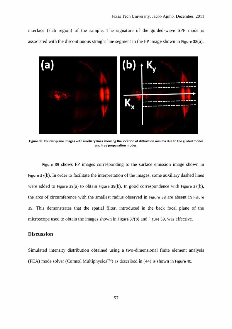
Texas Tech University, Jacob Ajimo, December, 2011
57
interface (slab region) of the sample. The signature of the guided-wave SPP mode is
associated with the discontinuous straight line segment in the FP image shown in Figure 38(a).
Figure 39: Fourier-plane images with auxiliary lines showing the location of diffraction minima due to the guided modes and free propagation modes.
Figure 39 shows FP images corresponding to the surface emission image shown in
Figure 37(b). In order to facilitate the interpretation of the images, some auxiliary dashed lines
were added to Figure 39(a) to obtain Figure 39(b). In good correspondence with Figure 37(b),
the arcs of circumference with the smallest radius observed in Figure 38 are absent in Figure
39. This demonstrates that the spatial filter, introduced in the back focal plane of the
microscope used to obtain the images shown in Figure 37(b) and Figure 39, was effective.
Discussion
Simulated intensity distribution obtained using a two-dimensional finite element analysis
(FEA) mode solver (Comsol Multiphysics™) as described in (44) is shown in Figure 40.
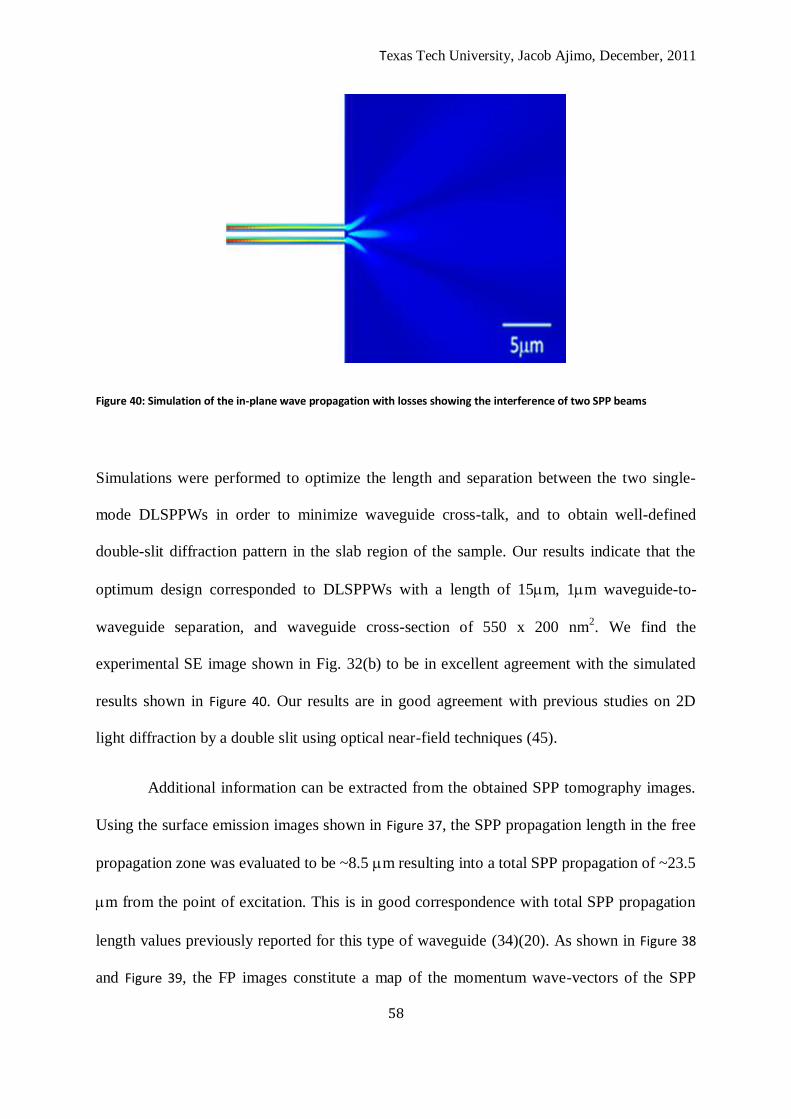
Texas Tech University, Jacob Ajimo, December, 2011
58
Figure 40: Simulation of the in-plane wave propagation with losses showing the interference of two SPP beams
Simulations were performed to optimize the length and separation between the two single-
mode DLSPPWs in order to minimize waveguide cross-talk, and to obtain well-defined
double-slit diffraction pattern in the slab region of the sample. Our results indicate that the
optimum design corresponded to DLSPPWs with a length of 15m, 1m waveguide-to-
waveguide separation, and waveguide cross-section of 550 x 200 nm2. We find the
experimental SE image shown in Fig. 32(b) to be in excellent agreement with the simulated
results shown in Figure 40. Our results are in good agreement with previous studies on 2D
light diffraction by a double slit using optical near-field techniques (45).
Additional information can be extracted from the obtained SPP tomography images.
Using the surface emission images shown in Figure 37, the SPP propagation length in the free
propagation zone was evaluated to be ~8.5 m resulting into a total SPP propagation of ~23.5
m from the point of excitation. This is in good correspondence with total SPP propagation
length values previously reported for this type of waveguide (34)(20). As shown in Figure 38
and Figure 39, the FP images constitute a map of the momentum wave-vectors of the SPP
Texas Tech University, Jacob Ajimo, December, 2011
59
excited at the sample surface. The magnitude of the wave-vectors (kSPP) can be easily
extracted from the FP images by measuring the distance (dSPP) from the trace corresponding
to each SPP excitation to the center of the dashed circumferences shown in Figure 38(b). We
used the transfer matrix method (9)(5) to calculate the value of kSPP for the SPP excited at the
gold-air interface. This value together with the radius of the smallest circumference shown in
Figure 38(b) allowed us to obtain a calibration constant of α = 1.39 × 10⁻⁵
nm-1
/pixel. Using
this approach and the following formulas:
SPP SPPk d (1)
2,SPP
SPPk
(2)
o
eff
SPP
n
(3)
eff
SPP
s
nArcSin
n
(4)
with λo = 632.8 nm, and a substrate refractive index value of ns = 1.525, we calculated from
the radius of the biggest circumference shown in Figure 38(b) a SPP wavelength, effective
refractive index, and resonance angle of λSPP ~ 541 nm, neff ~ 1.16, and θSPR ~ 500,
respectively, for the SPP propagating in the slab region. This is in a good agreement with the
calculated value of θSPR = 49.80
obtained using the transfer matrix method. Similarly, for the
guided-wave SPP mode we obtained values of λSPP ~ 593.9 nm, neff ~ 1.07, and θSPR ~ 44.30
using the shortest distance from the discontinuous straight line to the origin of wave-vector
Texas Tech University, Jacob Ajimo, December, 2011
60
coordinates shown in Figure 39(b). It is worth noting that the FP image signature of a single
beam confined in the DLSPPW corresponds to a single straight line segment.
However, the guided-wave SPP mode due to two beams is apparently represented in Figure
39 by a discontinuous straight line in the FP. This is a consequence of the out-of-plane
interference, at the screen of the back focal plane CCD camera, between the light that leaked
from both DLSPPWs (43). As shown in Figure 39(b), the values of ky, for which the minima of
interference occur in the out-of-plane double-slit diffraction pattern (discontinuous straight
line), are equal to its values along the interrupted arc of circumference, which is the signature
in the BP image of the in-plane SPP double-slit diffraction pattern observed in Figure 38. This
demonstrates that in both cases the position of the interference minima is inversely
proportional to the separation of the slits. In addition, Figure 39 shows clearly that the
dispersion in the values of ky produced by diffraction, which is determined by the width of the
slits, is also equal in both cases.
Partial conclusions We have shown the results of non-disturbing observation of SPP diffraction by a
double slit using SPP tomography. We presented a detailed discussion on how to extract the
quantitative values of the parameters that characterize the propagation, diffraction and
interference of SPP at the surface of the fabricated samples from the obtained images. Our
observations confirm previous studies on 2D diffraction by a double slit using optical near-
field techniques. Moreover, we found conclusive experimental evidence demonstrating that
2D light is diffracted by a SPP double slit in a similar way as three-dimensional
arrangements.
Texas Tech University, Jacob Ajimo, December, 2011
61
Plasmonic implementation of a quantum eraser for imaging
applications
Introduction
The pursuit of knowledge concerning the fundamentals of quantum mechanics has largely
motivated the interest on quantum erasers (46-47). Experiments with quantum erasers helped
to establish that which-path information and visibility of interference fringes are
complementary quantities: any distinguishability between the paths of interfering beams of
light destroys the quality (visibility) of the interference fringes (47). In the simplest quantum
eraser (48), diffraction of light by a double-slit experiment with a vertical polaroid placed
before one slit and a horizontal polaroid before the other one did not display interference
fringes because the path through each slit is labeled by orthogonal states of polarization. The
which-path information may be removed and the interference restored by placing a polaroid
oriented at 45° angle with respect to the vertical direction somewhere between the two-slit
screen and the detection screen.
In this work, we describe a quantum eraser for non-disturbing imaging the
interference pattern formed when two perpendicular surface plasmon polariton (SPP) beams
cross each other. We implemented the quantum eraser using a leakage radiation microscope
(LRM). In order to excite SPPs that propagate in the metal-air interface of a fabricated
sample, the excitation light was focused in scattering features patterned in the sample surface
using a low numerical aperture objective lens (12)(35). Collection of the SPP-coupled
radiation that leaks to the sample glass substrate during the propagation of SPPs along the
metal-air interface was done using an immersion oil objective lens with high numerical
aperture (12-14)(35). Leakage radiation microscopy is an ideal technique to study the
propagation of SPPs because the photons used for imaging are the ones that regardless of the
measurement process leak into the sample substrate. This can be advantageously used for
non-disturbing observation of SPP propagation. In alternative state of the art methods for
imaging SPP propagation, such as near-field scanning optical microscopes (17), an optical tip
is often placed in close proximity to the region to be imaged, which introduces unavoidable
perturbations in the original distribution of electromagnetic fields in the sample. We show
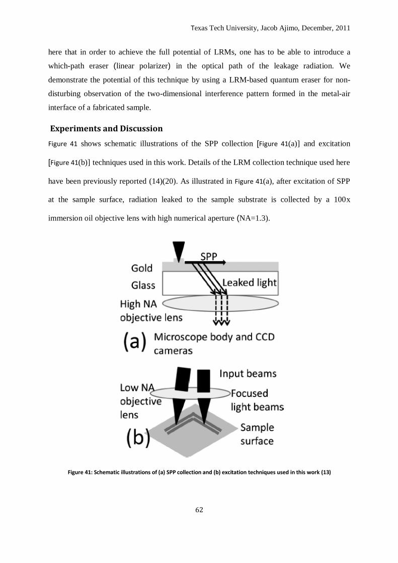
Texas Tech University, Jacob Ajimo, December, 2011
62
here that in order to achieve the full potential of LRMs, one has to be able to introduce a
which-path eraser (linear polarizer) in the optical path of the leakage radiation. We
demonstrate the potential of this technique by using a LRM-based quantum eraser for non-
disturbing observation of the two-dimensional interference pattern formed in the metal-air
interface of a fabricated sample.
Experiments and Discussion
Figure 41 shows schematic illustrations of the SPP collection [Figure 41(a)] and excitation
[Figure 41(b)] techniques used in this work. Details of the LRM collection technique used here
have been previously reported (14)(20). As illustrated in Figure 41(a), after excitation of SPP
at the sample surface, radiation leaked to the sample substrate is collected by a 100x
immersion oil objective lens with high numerical aperture (NA=1.3).
Figure 41: Schematic illustrations of (a) SPP collection and (b) excitation techniques used in this work (13)
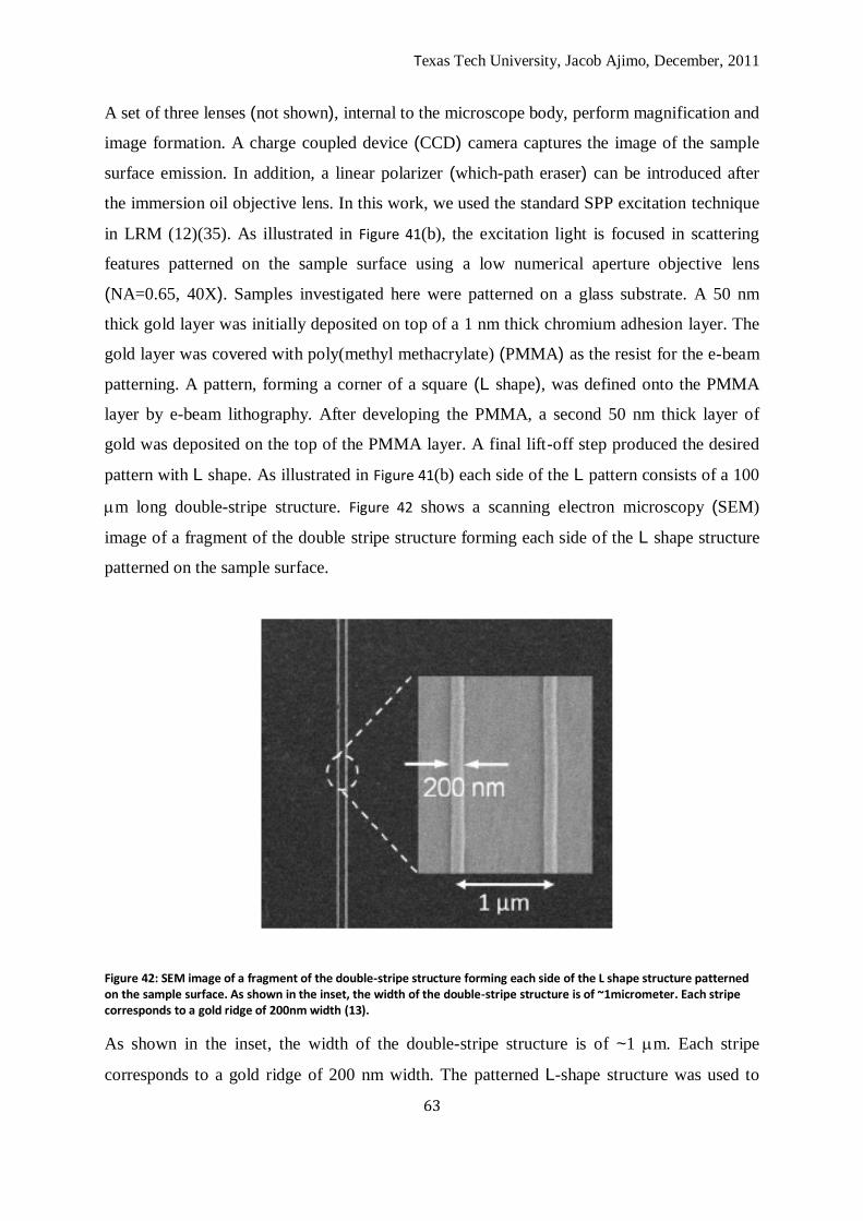
Texas Tech University, Jacob Ajimo, December, 2011
63
A set of three lenses (not shown), internal to the microscope body, perform magnification and
image formation. A charge coupled device (CCD) camera captures the image of the sample
surface emission. In addition, a linear polarizer (which-path eraser) can be introduced after
the immersion oil objective lens. In this work, we used the standard SPP excitation technique
in LRM (12)(35). As illustrated in Figure 41(b), the excitation light is focused in scattering
features patterned on the sample surface using a low numerical aperture objective lens
(NA=0.65, 40X). Samples investigated here were patterned on a glass substrate. A 50 nm
thick gold layer was initially deposited on top of a 1 nm thick chromium adhesion layer. The
gold layer was covered with poly(methyl methacrylate) (PMMA) as the resist for the e-beam
patterning. A pattern, forming a corner of a square (L shape), was defined onto the PMMA
layer by e-beam lithography. After developing the PMMA, a second 50 nm thick layer of
gold was deposited on the top of the PMMA layer. A final lift-off step produced the desired
pattern with L shape. As illustrated in Figure 41(b) each side of the L pattern consists of a 100
m long double-stripe structure. Figure 42 shows a scanning electron microscopy (SEM)
image of a fragment of the double stripe structure forming each side of the L shape structure
patterned on the sample surface.
Figure 42: SEM image of a fragment of the double-stripe structure forming each side of the L shape structure patterned on the sample surface. As shown in the inset, the width of the double-stripe structure is of ~1micrometer. Each stripe corresponds to a gold ridge of 200nm width (13).
As shown in the inset, the width of the double-stripe structure is of ~1 m. Each stripe
corresponds to a gold ridge of 200 nm width. The patterned L-shape structure was used to
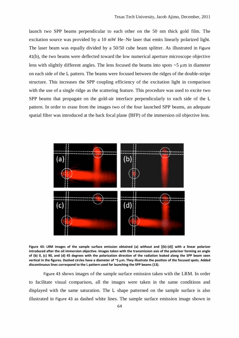
Texas Tech University, Jacob Ajimo, December, 2011
64
launch two SPP beams perpendicular to each other on the 50 nm thick gold film. The
excitation source was provided by a 10 mW He–Ne laser that emits linearly polarized light.
The laser beam was equally divided by a 50/50 cube beam splitter. As illustrated in Figure
41(b), the two beams were deflected toward the low numerical aperture microscope objective
lens with slightly different angles. The lens focused the beams into spots ~5 m in diameter
on each side of the L pattern. The beams were focused between the ridges of the double-stripe
structure. This increases the SPP coupling efficiency of the excitation light in comparison
with the use of a single ridge as the scattering feature. This procedure was used to excite two
SPP beams that propagate on the gold-air interface perpendicularly to each side of the L
pattern. In order to erase from the images two of the four launched SPP beams, an adequate
spatial filter was introduced at the back focal plane (BFP) of the immersion oil objective lens.
Figure 43: LRM images of the sample surface emission obtained (a) without and [(b)-(d)] with a linear polarizer introduced after the oil immersion objective. Images taken with the transmission axis of the polarizer forming an angle of (b) 0, (c) 90, and (d) 45 degrees with the polarization direction of the radiation leaked along the SPP beam seen
vertical in the figures. Dashed circles have a diameter of ~5 m. They illustrate the position of the focused spots. Added discontinuous lines correspond to the L pattern used for launching the SPP beams (13).
Figure 43 shows images of the sample surface emission taken with the LRM. In order
to facilitate visual comparison, all the images were taken in the same conditions and
displayed with the same saturation. The L shape patterned on the sample surface is also
illustrated in Figure 43 as dashed white lines. The sample surface emission image shown in
Texas Tech University, Jacob Ajimo, December, 2011
65
Figure 43(a) was obtained without adding a polarizer in the optical path of the leakage
radiation. Two perpendicular SPP beams crossing each other are clearly seen. The image is
formed on the microscope CCD camera by the SPP-coupled radiation that leaks from any
point of the sample metal-air interface that the SPP excitation passes through. Regardless of
the polarization direction of the linearly polarized light emitted by the laser source, only the
fraction of the input light that is scattered with TM polarization (by the L shape structure
patterned on the sample surface) can excite SPPs. Consequently, as long as the two SPP
beams are excited simultaneously in the metal-air interface of the sample, we expect to
observe clear interference fringes in the region where the two SPP beams cross each other.
However, this is hardly the case in Figure 43(a). The absence of clear interference fringes in
Figure 43(a) is due to the different states of polarization of the leakage radiation. The direction
of the electric field of the light that leaks along one of the SPP beams is perpendicular to the
direction of the electric field of the light that leaks along the other beam. This well known
property was verified by introducing a linear polarizer after the BFP of the immersion oil
objective lens. As shown in Figure 43(b) and Figure 43(c), the insertion of a linear polarizer,
with the transmission axis parallel to the polarization direction of the light leaked along the
direction of propagation of one of the beams, results in the erasure of the another beam from
the surface emission image. Thus, the polarization state of the photons arriving at the CCD
camera can be used for identifying the path followed by the leaked photons. This smear out
the interference fringes actually existing at the metal-air interface of the sample from the
image of it formed at the CCD camera [see Figure 43(a)]. The intensity profile along the center
of each SPP beam was measured and fitted to an exponential decay curve to determine the
SPP propagation length in the sample. We determined a propagation length of ~11 m in
good correspondence with reported values of ~10 m for thin gold films in the visible
range(1)(49). In addition, we performed a two-dimensional finite element simulation of SPP
propagation (9). In good correspondence with the experimentally determined value, a
propagation length of 9.3 m was obtained from the simulation. A total observable
propagation length of ~25 m was verified in our experiments (see Figure 43).
In order to erase the which-path information, we rotated the transmission axis of the
linear polarizer 45° angle with respect to the polarization directions of the leakage radiation.
After removing the which-path information with the polarizer, as shown in Figure 43(d), well-
defined interference fringes are observed in the region of the sample surface emission image
where the two beams cross each other. The separation between consecutive interference
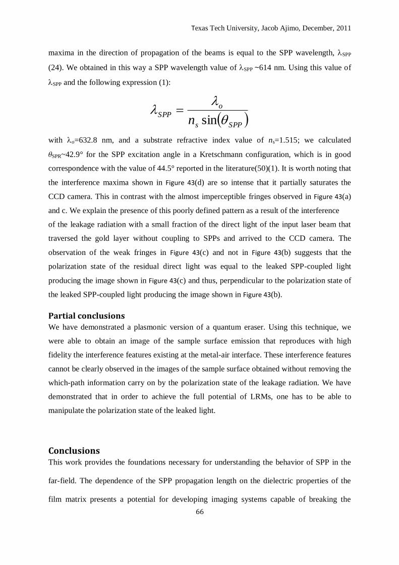
Texas Tech University, Jacob Ajimo, December, 2011
66
maxima in the direction of propagation of the beams is equal to the SPP wavelength, SPP
(24). We obtained in this way a SPP wavelength value of SPP ~614 nm. Using this value of
SPP and the following expression (1):
SPPs
oSPP
n
sin
with o=632.8 nm, and a substrate refractive index value of ns=1.515; we calculated
SPR~42.9° for the SPP excitation angle in a Kretschmann configuration, which is in good
correspondence with the value of 44.5° reported in the literature(50)(1). It is worth noting that
the interference maxima shown in Figure 43(d) are so intense that it partially saturates the
CCD camera. This in contrast with the almost imperceptible fringes observed in Figure 43(a)
and c. We explain the presence of this poorly defined pattern as a result of the interference
of the leakage radiation with a small fraction of the direct light of the input laser beam that
traversed the gold layer without coupling to SPPs and arrived to the CCD camera. The
observation of the weak fringes in Figure 43(c) and not in Figure 43(b) suggests that the
polarization state of the residual direct light was equal to the leaked SPP-coupled light
producing the image shown in Figure 43(c) and thus, perpendicular to the polarization state of
the leaked SPP-coupled light producing the image shown in Figure 43(b).
Partial conclusions
We have demonstrated a plasmonic version of a quantum eraser. Using this technique, we
were able to obtain an image of the sample surface emission that reproduces with high
fidelity the interference features existing at the metal-air interface. These interference features
cannot be clearly observed in the images of the sample surface obtained without removing the
which-path information carry on by the polarization state of the leakage radiation. We have
demonstrated that in order to achieve the full potential of LRMs, one has to be able to
manipulate the polarization state of the leaked light.
Conclusions This work provides the foundations necessary for understanding the behavior of SPP in the
far-field. The dependence of the SPP propagation length on the dielectric properties of the
film matrix presents a potential for developing imaging systems capable of breaking the
Texas Tech University, Jacob Ajimo, December, 2011
67
diffraction limit. The use of the back focal plane provides the background of studying
electromagnetic band gap materials. Interference and diffraction effects are fundamental
wave nature characteristics that open an avalanche of applications of SPPs in a number of
areas. While it does not claim a complete characterization of SPPs in the far-field, this work
should provide valuable information for more specific study of the SPP behavior especially
metamaterials by using plasmon tomography.
In a nutshell, the following conclusions can be obtained from this dissertation; SPP
excitation and characterization have been presented and discussed; The use of plasmon
tomography presents a simple and effective way of SPP characterization in the far-field;
Plasmonic version of the quantum eraser was demonstrated; Effect of walls on the diffraction
pattern due to two beams was displayed and discussed; The double slit experiment was
demonstrated in the far-field using plasmon tomography; Polarization states of SPP modes
were identified and demonstrated.
Texas Tech University, Jacob Ajimo, December, 2011
68
Bibliography
1. Raether, H. Surface plasmons on smooth and rough surfaces and on gratings. New York : Springer-
Verlag, 1988.
2. Challener, Dror Sarid and William. Modern introduction to Surface Plasmons Theory,
Mathematica Modelling and Applications. New York : Cambridge University Press, 2010.
3. Maier, Stefan A. Plasmonics: Fundamentals and Applications. New york : Springer, 2007.
4. Surface plasmon polariton analogue to Young's double-slit experiment. Brongersma, Rashid Zia
and Mark L. 2007, Nature Nanotechnology, Vol. 2.
5. Thin-Films field-transfer matrix theory of planar multilayer waveguides and reflection from prism-
loaded waveguides. Hodgkinson, J. Chilwell and I. 742, s.l. : Journal of Optical society of America A,
1984, Journal of Optical society of America A, Vol. 1.
6. Leakage radiation microscopy of surface plasmon polaritons. A. Drezet, A. Hehenau, D. Koller, A.
Stepanov, H. Ditlbacher, B. Steinberger, F. R. Aussnegg, A. Leitner, J. R. Krenn. 220, 2008, Materials
Science and Engineering B, Vol. 149.
7. Resonant Coupling in Dielectric Loaded Plasmonic Waveguide Devices. A. Krishnan, C. J. Regan, L.
Grave de Peralta and A. A. Bernussi. 231110, 2010, Applied Physics Letters, Vol. 97.
8. Study of interference in a double-slit without walls by plasmon tomography techniques. J. Ajimo,
C. J. Regan, A. C. Bernussi, S. Park, R. Lopez-Boada, A. A. Bernussi and Grave de Peralta. 2011,
Optics Communications, Vol. 284, pp. 4752-4755.
9. Comment on does the leakage radiation profile mirror the intensity profile of surface plasmon
polaritons? Peralta, L. Grave de. 13, 2011, Optics Letters, Vol. 36, p. 2516.
10. Image formation in Widefield Microscope Based on Leakage of surface plasmon-Coupled
Fluorescence. S.P Frisbie, C.F. Chestnut, M. E. Holtz, A. Krishnan, L. Grave de Peralta and A. A.
Bernussi. 2, s.l. : IEEE Photonis Journal, 2009, IEEE Photonis Journal, Vol. 1.
11. Dielectric-loaded surface plasmon polariton waveguides: Figures of merit and mode
characterization by image and Fourier plane leakage microscopy. J. Grandidier, S. Massenot, G.
Colas des Francs, A. Bouhelier, J.-C. Weeber, L. Markey, A. Dereux, J. Renger, M. U. Gonzalez, and
R. Quidant. 245419, s.l. : Physical Reviews:B, 2008, Physical Reviews:B, Vol. 78.
12. Charaterization of polarization states of surface plasmon polariton modes by Fourier-plane
leakage microscopy. S.P. Frisbie, C.J. Regan, A. Krishnan, C. Chestnut, J. Ajimo, A.A. Bernussi, L.
Grave de Peralta. 2010, Optics Communications, Vol. 283.

Texas Tech University, Jacob Ajimo, December, 2011
69
13. Plasmonic Impelementation of a quantum eraser for imaging applications. J. Ajimo. M.
Marchante, A. Krishnan, A. A. Bernussi, and L. Grave de Peralta. 2010, Journal of Applied Physics,
pp. 063110-063110-3.
14. Nano-optics of surface plasmon polaritons. Anatoly V. Zayats, Igor I. Smolyaninov, Alex A.
Maradudin. 2005, Physics Reports, Vol. 408.
15. Efficient Unidirectional nanoslit couplers for surface plasmons. F. Lopez Tejeira, Sergie G.
Rodrigo, L. Martin-Moreno, F. J. Garcia-Vidal, E. Devaux, T. W. Ebbesen, J. R. Krenn, I. P. Radko, S.
I. Bozhevolnyi, M. U. Gonzalel, J. C. Weeber and A. Dereux. 2007, Nature Physics, Vol. 3.
16. Plasmonics: Merging Photonics and Elelctronics at Nanoscale Dimensions. Ozbay, Ekmel. 2006,
Science, Vol. 311, pp. 189-193.
17. Surface plasmon polariton analogue to Young's double slit experiment. Zia, Rashid. 2007, Nature,
pp. 426-429.
18. Optical Reflectivity of Asymmetric Dielectric-Metal-Dielectric Planar Structures. Stephen P.
Frisbie, Ananth Krishnan. Xiaoyan Xu, Luis Grave de Peralta, Sergey A. Nikishin, Mark W. Holtz and
Ayrton A. Bernussi. 15, 2009, Journal of Lightwave Technology, Vol. 27.
19. Plasmonics for near-field nano-imaging and superlensing. Satoshi Kawata, Yasushi and Prabhat
Verma. 2009, Nature Photonics, Vol. 3, pp. 388-394.
20. Frisbie, S. P. Imaging of surface plasmon-coupled fluorescence and optical reflectivity of
dielectric-metal-dielectric structures. s.l. : Doctoral dissertation, Texas Tech University, 2009.
21. Wolf, M. Born and E. Principles of Optics. New York : Pergamon Press, 1964.
22. S, Heavens. O. Optical properties of thin solid films. London : Butterworths Scientific Publications,
1955.
23. K., Sharma. K. Optics Principles and Applications. New York : Elsevier, 2006.
24. Hagness, Allen Taflove and Susan C. Computational electrodynamics the finite-difference time-
domain method. Boston : Artech House, 2005.
25. How to erase surface plasmon fringes. A. Drezet, A. Hohenau, A. L. Stepanov, H. Ditlbacher, B.
Steinberger, N. Galler, F.R Aussenegg, A. Leitner, and J. R. Krenn. 091117, 2006, Applied Physics
Letters, Vol. 89.
26. Polymer-metal waveguides Characterization by Fourier plane leakage radiation microscopy. S.
Massenot, J. Grandidier, A. Bouhelier, G. Colas des Francs, L. Markey, J.-C. Weeber, A. Dereux, J.
Renger, M. U. Gonzalez, and R. Quidant. 243102, 2007, Applied Physics Letters, Vol. 91.
27. Plasmon Stimulated Emission in Arrays of Bimetallic Structures Coated with Dye-Doped Dielectric.
A. Krishnan, S.P. Frisbie, L. Grave de Peralta, and A. A. Bernussi. 111104, 2010, Applied Physics
Letters, Vol. 96.
Texas Tech University, Jacob Ajimo, December, 2011
70
28. Optical stethoscopy: Image recording with lambda/20. D. W. Pohl, W. Denk, M. Lanz. 651, s.l. :
Applied Physics Letters, 1984, Applied Physics Letters, Vol. 44.
29. J. Gryczinski, K. Malicka, Z. Nowaczyk, J. Gryczynski, J. Lacowicz. s.l. : Physical Chemistry B,
2004, Physical Chemistry B, Vol. 108.
30. Surface Plasmon-Coupled Emission with Gold Films. I. Gryczynski, J. Malicka, Z. Gryczynski, J.R.
Lakowicz. 33, 2004, Journal of Physical Chemistry B, Vol. 108, pp. 12568-12574.
31. J. Gryczynski, K. Malicka, Z. Nowaczyk, J. Lakowicz. 12073, s.l. : Physical Chemistry B, 2004, Vol.
108.
32. I. Gryczynski, J. Malicka, K. Nowaczyk, Z. Gryczynski, J.R. Lakowicz. 15, 2006, Thin Solids Films,
Vol. 510.
33. F. L. Pedrotti, L.S. Pedrotti. Introduction to Optics. New Jersey : Prentice Hall, 2007.
34. Giancoli, D.G. Physics: Principles with applications, 6th Ed. New Jersey : Pearson Prentice Hall,
2005.
35. A. Giambattisa, B.M. Richardson, R.C Richardson. College Physics: With an integrated Approach
to Forces and Kinematics, 3rd Ed. New York : Mc Graw Hill, 2007.
36. Walker, J.S. Physics. 4th Ed. New York : Addison-Wesley, 2008.
37. Ultrafast response of arrayed waveguide grating pulse shapers with digital amplitude and phase
modulation. L. Grave de Peralta, A.A. Bernussi, H. Temkin. 2410, 2007, IEEE Journal of Lightwave
Technology, Vol. 25.
38. Utrafast response of arrayed waveguide grating. L. Grave de Peralta, A.A. Bernussi, H. Temkin.
473, 2007, IEEE Journal of Quantum Electronics, Vol. 43.
39. Interference in wave-front-division-based spectrometers illuminated with ultra fast pulses of
light. Peralta, L. Grave de. 013111, 2009, Journal of Applied Physics, Vol. 105.
40. Phenomonological quantum description of the ultra fast response of arrayed waveguide gratings.
Peralta, L. Grave de. 103110, 2010, Journal of Applied Physics, Vol. 108.
41. Some consequences of experiments with plasmonic quantum eraser for plasmon tomography. L.
Grave de Peralta, R. Lopez-Boada, A. Ruiz- Columbie, S. Park and A. A. Bernussi. 1, 2011, Journal of
Applied Physics, Vol. 109.
42. Study of interference between surface plasmon polaritons by leakage radiation microscopy.
Peralta, Luis Grave de. 8, 2010, Journal of Optical Society of America B, Vol. 27.
43. Generation os Surface Plasmons at single subwavelength slits: from slit to ridge plasmons. J.-Y.
Laluet, A. Drezet, C. Genet, T.W. Ebbesen. 105014, 2008, New Journal of Physics, Vol. 10.
Texas Tech University, Jacob Ajimo, December, 2011
71
44. Qualitative analysis of surface plasmon interaction with silver nanoparticles. A.L. Stepanov, J.R.
Krenn, H. Ditlbacher, A. Hohenau, A. Drezet, B. Steinberger, A. Leitner, F.R. Aussenegg. 1524, 2005,
Optics Letters, Vol. 20.
45. R.P. Feynman, R.B. Leighton, M. Sands. The Feynman Lectures in Physics. New York : Addison-
Wesley, 1966. Vol. III.
46. —. The Feynman Lectures in Physics. New York : Addison-Wesley, 1966. Vol. I.
47. Surface Plasmon Sensor Based on Enhanced Light Transmission Through Arrays of Nanoholes in
Gold Films. Alexander G. Brolo, Reuven Gordon, Brian Leathem and Karen L. Kavanagh. 2004,
Langmuir, Vol. 20, pp. 4812-4815.
48. Finite element analysis of lossless propagation in surface plasmon polariton waveguides with
nanoscale spot-sizes. A. Krishnan, L. Grave de Peralta, M. Holtz and A.A. Bernussi. 1114, 2009,
Journal of Lightwave Technology, Vol. 27.
49. Complementarity and the Quantum eraser. T. J. Herzog, P. G. Kwiat, H. Weinfurter and A.
Zeilinger. 3034, 1995, Physical Review Letters, Vol. 75.
50. Double-slit quantum eraser. S. P. Walborn, M. O. Terra Cunha, S. Padua and C.H. Monken.
033818, 2002, Physical Review A, Vol. 65.
51. A simple quantum Eraser. Holladay, W. 280, 1993, Physics Letters A, Vol. 183, pp. 280-282.
52. Elongation of surface plasmon polaritons propagation length without gain. G. Zhu, M. Mayy, M.
Bahoura, B. A. Ritzo, H. V Gavrilenko, V. I. Gavrilenko, M. A. Noginov. 15576, 2008, Optics Express,
Vol. 16.
53. Propagation Length of surface plasmons in a metal film with roughness. A. Kolomenski, A.
Kolomenskii, J. Noel, S. Peng and H. Schuessler. 5683, 2009, Applied Optics, Vol. 48.
54. Dielectric loaded surface plasmon polariton waveguides: Figures of merit and . J. grandidier, S.
Massenot, G. Colas des Francs, A. Bouhelier, J.-C. Weeber, L. Markey, A. Dereux, J. Renger, M. U.
Gonzalez, and R. Quidant.
55. Quantum eraser: A proposed photon correlation experiment concerning observation of delayed
choice in quantum mechanics. Druhl, M. O. Scully and K. 2208, 1982, Physical reviews A, Vol. 25.
56. How to erase surface plasmon fringes. Aurelien Drezet, Andreas Hohenau, Audrey L. Stepanov,
Harald Ditlbacher, Bernhard Steinberger, Nicole Galler, Franz R Aussenegg, Alfred Leitner and
Joachim R. Krenn. 091117, 2006, Applied Physics Letters, Vol. 89.
57. Surface Plasmon resonance-based Fiber and Planar Waveguide Sensors. Nemova, Raman
Kashyap and Galina. 2009, Journal of Sensors.
58. I.Gryczynski, S. Massenot, G. Colas des Francs, A. Bouhelier, j.-C. Weeber, L. Markey, A. Dereux,
J. Renger, M. U. Gonzalez, R. Quidant. 245419, 2008, Physical Reviews B, Vol. 78.