Embed Size (px)
DESCRIPTION
diffrent planel
Citation preview

Solar Panel:-
Solar Panel is technically known PV panels or Photovoltaic panel. The term photovoltaic coming from two words i.e. photo means light and voltaic means electricity. It can convert from light energy to electrical energy in terms of direct current (dc).But normal light can produce only voltage and very less amount of current. But Sunlight produces both voltage and current efficiently due to presence of photon in sun light.
PV TEHCHNOLOGY
Photovoltaic (PV) solar cells as they are often referred to, are semiconductor devices that convert sunlight into direct current (DC) electricity. Groups of PV cells are electrically configured into modules and arrays, which can be used to charge batteries, operate motors, and to power any number of electrical loads. With the appropriate power conversion equipment, PV systems can produce alternating current (AC) compatible with any conventional appliances, and operate in parallel with and interconnected to the utility grid.
HISTORY OF PHOTOVOLTAIC
The first conventional photovoltaic cells were produced in the late 1950s, and throughout the 1960s were principally used to provide electrical power for earth-orbiting satellites.
In the 1970s, improvements in manufacturing, performance and quality of PV modules helped to reduce costs and opened up a number of opportunities for powering remote terrestrial applications, including battery charging for navigational aids, signals, telecommunications equipment and other critical, low power needs. In the 1980s, photovoltaic became a popular power source for consumer electronic devices, including calculators, watches, radios, lanterns and other small battery charging applications. Following the energy crises of the 1970s, significant efforts also began to develop PV power systems for residential and commercial uses both for stand-alone, remote power as well as for utility-connected applications. During the same period, international applications for PV systems to power rural health clinics, refrigeration, water pumping, telecommunications, and off-grid households increased dramatically, and remain a major portion of the present world market for PV products. Today, the industry’s production of PV modules is growing at approximately 25 percent annually, and major programs in the U.S., Japan and Europe are rapidly accelerating the implementation of PV systems on buildings and interconnection to utility networks.

A solar panel is a device that collects photons of sunlight, which are very small packets of electromagnetic radiation energy, and converts them into electrical current that can be used to power electrical loads.
Using solar panels is a very practical way to produce electricity for many applications. The obvious would have to be off-grid living. Living off-grid means living in a location that is not serviced by the main electric utility grid. Remote homes and cabins benefit nicely from solar power systems. No longer is it necessary to pay huge fees for the installation of electric utility poles and cabling from the nearest main grid access point. A solar electric system is potentially less expensive and can provide power for upwards of three decades if properly maintained.
Besides the fact that solar panels make it possible to live off-grid, perhaps the greatest benefit that you would enjoy from the use of solar power is that it is both a clean and a renewable source of energy. With the advent of global climate change, it has become more important that we do whatever we can to reduce the pressure on our atmosphere from the emission of greenhouse gases.
Solar panels have no moving parts and require little maintenance. They are ruggedly built and last for decades when porperly maintained.Last, but not least, of the benefits of solar panels and solar power is that, once a system has paid for its initial installation costs, the electricity it produces for the remainder of the system’s lifespan, which could be as much as 15-20 years depending on the quality of the system, is absolutely free! For grid-tie solar power system owners, the benefits begin from the moment the system comes online, potentially eliminating monthy electric bills or, and this is the best part, actually earning the system’s owner additional income from the electric company.
The solar cells you would have seen on satellites, caculaters etc are photovoltaic cells or modules (modules are a collection of solar cells electrically connected and joined together in one frame). Photovoltaics, (photo = light, voltaic = electricity), convert the energy of sunlight directly into electricity. Originally expensive and only used in space, photovoltaics are now finding many applications on countless devices, buildings etc were ever remote or free and environmentally sustainable produced electricity is required.

Photovoltaic (PV) cells are made of special materials called semiconductors like silicon, which is currently the most commonly used. Basically, when light shines on the solar cell a percentage of this solar energy is absorbed into the semiconductor material. This energy now inside the semiconductor knocks electrons loose allowing them to flow freely. PV cells also all have one or more electric fields

that force electrons freed by light absorption to flow in a certain direction. This flow of electrons is an electrical current. Metal contacts on the top and bottom of the PV cell draw that current off to use to power external electrical products such as lights, calculators etc. This current ,combined with the cell’s voltage (which is a result of its built-in electric field or fields),determines the power (or wattage) that the solar cell can produce.
Solar panels collect clean renewable energy in the form of sunlight and convert that light into electricity which can then be used to provide power for electrical loads. Solar panels are comprised of several individual solar cells which are themselves composed of layers of silicon, phosphorous (which provides the negative charge), and boron (which provides the positive charge). Solar panels absorb the photons and in doing so initiate an electric current. The resulting energy generated from photonsstriking the surface of the solar panel allows electrons to be knocked out of their atomic orbits and released into the electric field generated by the solar cells.
An average home has more than enough roof area for the necessary number of solar panels to produce enough solar electricrity to supply all of its power needs. Assisted by an inverter, a device that converts the direct current (or DC current), generated by a solar panel into alternating current (or AC current), solar panel arrays can be sized to meet the most demanding electrical load requirements. The AC current can be used to power loads in your home or commercial building, your recreational vehicle or your boat (RV/Marine Solar Panels), your remote cabin or home, and remote traffic controls, telecommunications equipment, oil and gas flow monitoring, RTU, SCADA, and much more.
How to test a Solar Panel?
Most in the most people that need to set up solar panels at the roof of the properties consider that all they must do is set up them, however they overlook about assessment them after which if a little something won’t perform adequately they must phone for that installers once again and using this method they reduce time and get stressed.
Solar panel assessment pertains to employing an amp meter at the panel. power is acknowledged for being measured in amperes. This factor may be accomplished with an amp meter. this kind of a equipment are heading to be connected towards bad and good terminals at the solar panel after which the panel are heading to be subjected towards sunlight. In purchase to guard by yourself from injuries and protected the amp meter from any destruction you really should 1st price the meter greater compared to solar panel is. The amp meter will present you on its display ‘the brief circuit current’. This are heading to be the level of electric present-day that 1 could assume out of your panels to give. OF

program everything is established by how powerful was the sunshine so it can be indicted to conduct your solar panel assessment when there is ordinarily a complete sunshine outside.
Besides employing an amp meter you’ll be in a position to decide the energy yield of your respective solar panel by employing an additional strategy that implies measuring the resistor’s voltage. because of this solar panel assessment process you’ll require a electronic multi-meter (that actions the DC voltage) and numerous resistors. subsequent to acquiring every one among the essential measurements you’ll be in a position to use this formulation for calculating the energy output: present-day equals Voltage / Resistance. subsequent to that 1 could constitute a overall performance graphic by
plotting the energy output.
You really should also be mindful that a solar panel will transform the sunshine into DC (direct current) energy not AC energy as some may perhaps expect. it is why you require for that
solar panel assessment methods a DC electronic multi-meter.

Watts are heading to be applied for measuring the energy the fact that solar panel produced for charging electric batteries as an example or for employing dwelling appliances. The formulation for calculating the energy is energy equals Voltage*Current. All you’ve still left to perform is continually to measure the amperage and voltage of your respective solar panel and plug the info to the equation. using this method you’ll know precisely when the solar panel are heading to be in a placement to include every one among the power you desired it to supply you once you made a decision to set up this kind of a factor on your own roof.
You will even use a solar cost controller that could be designed for regulating the energy that could be brought through the solar panel towards rechargeable batteries. this kind of a controller has the intent of by-passing eventual overcharges also to present a very good power supply cost based at the temperatures outside. apart from solar panel assessment you really should also analyze the very well working of the cost controller.
If you consider you’ll be in a position to not conduct the solar panel assessment on your personal or you do not have time for that phone some panel installers and request them to perform this to match your needs because it may perhaps conserve you from numerous difficulty later on on.
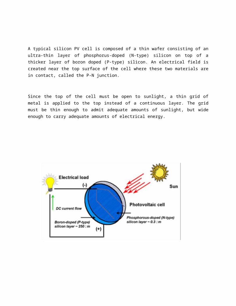
A typical silicon PV cell is composed of a thin wafer consisting of an ultra-thin layer of phosphorus-doped (N-type) silicon on top of a thicker layer of boron doped (P-type) silicon. An electrical field is created near the top surface of the cell where these two materials are in contact, called the P-N junction.
Since the top of the cell must be open to sunlight, a thin grid of metal is applied to the top instead of a continuous layer. The grid must be thin enough to admit adequate amounts of sunlight, but wide enough to carry adequate amounts of electrical energy.
Light, including sunlight, is sometimes described as particles called "photons." As sunlight strikes a photovoltaic cell, photons move into the cell.
When a photon strikes an electron, it dislodges it, leaving an empty "hole". The loose electron moves toward the top layer of the cell. As photons continue to enter the cell, electrons continue to be dislodged and move upwards.
If an electrical path exists outside the cell between the top grid and the back plane of the cell, a flow of electrons begins. Loose electrons move out the top of the cell and into the external electrical circuit. Electrons from further back in the circuit move up to fill the empty electron holes.
Most cells produce a voltage of about one-half volt, regardless of the surface area of the cell. However, the larger the cell, the more current it will produce.
The resistance of the circuit of the cell will affect the current and voltage. The amount of available light affects current production. The temperature of the cell affects its voltage.
Regardless of size, a typical silicon PV cell produces about 0.5 – 0.6 volt DC under open-circuit, no-load conditions. The current (and power) output of a PV cell depends on its efficiency and size (surface area), and is proportional to the intensity of sunlight striking the surface of the cell. For example, under peak

sunlight conditions a typical commercial PV cell with a surface area of 160 cm^2 (~25 in^2) will produce about 2 watts peak power. If the sunlight intensity were 40 percent of peak, this cell would produce about 0.8 watts.
TYPES OF PV CELLS
The four general types of photovoltaic cells are:
Single-crystal silicon. Polycrystalline silicon (also known as multicrystalline silicon). Ribbon silicon. Amorphous silicon (abbreviated as "aSi," also known as thin film silicon).
Single-crystal silicon:
Most photovoltaic cells are single-crystal types. To make them, silicon
is purified, melted, and crystallized into ingots. The ingots are sliced into thin wafers to make
individual cells. The cells have a uniform color, usually blue or black.

Polycrystalline silicon:
Polycrystalline cells are manufactured and operate in a similar manner. The difference is that lower cost silicon is used. This usually results in slightly lower efficiency, but polycrystalline cell manufacturers assert that the cost benefits outweigh the efficiency losses. The surface of polycrystalline cells has a random pattern of crystal borders instead of the solid color of single crystal cells.
Ribbon silicon :
Growing a ribbon from the molten silicon instead of an ingot makes ribbon-type photovoltaic cells. These cells operate the same as single and polycrystal cells.
The anti-reflective coating used on most ribbon silicon cells gives them a prismatic rainbow appearance.

Amorphous or thin film silicon: The previous three types of silicon used for photovoltaic cells have a distinct crystal structure. Amorphous silicon has no such structure. Amorphous silicon is sometimes abbreviated "aSi" and is also called thin film silicon.
Amorphous silicon units are made by depositing very thin layers of vaporized silicon in a vacuum onto a support of glass, plastic, or metal.
PHOTOVOALTAIC MODULES
For almost all applications, the one-half volt produced by a single cell is inadequate. Therefore, cells are connected together in series to increase the voltage. Several of these series strings of cells may be connected together in parallel to increase the current as well.
These interconnected cells and their electrical connections are then sandwiched between a top layer of glass or clear plastic and a lower level of plastic or plastic and metal. An outer frame is attached to increase mechanical strength, and to provide a way to mount the unit. This package is called a "module" or "panel" . Typically, a module is the basic building block of photovoltaic systems.
Groups of modules can be interconnected in series and/or parallel to form an "array." By adding "balance of system" (BOS) components such as storage batteries, charge controllers, and power conditioning devices, we have a complete photovoltaic system.

Describing photovoltaic module performance
To insure compatibility with storage batteries or loads, it is necessary to know the electrical characteristics of photovoltaic modules.
Consider "I" is the abbreviation for current, expressed in amps. "V" is used for voltage in volts, and "R" is used for resistance in ohms.
A photovoltaic module will produce its maximum current when there is essentially no resistance in the circuit. This would be a short circuit between its positive and negative terminals.
This maximum current is called the short circuit current, abbreviated I(sc). When the module is shorted, the voltage in the circuit is zero.Conversely, the maximum voltage is produced when there is a break in the circuit. This is called the open circuit voltage, abbreviated V(oc). Under this condition the resistance is infinitely high and there is no current, since the circuit is incomplete.
These two extremes in load resistance, and the whole range of conditions in between them, are depicted on a graph called a I-V (current-voltage) curve. Current, expressed in amps, is on the vertical Y-axis. Voltage, in volts, is on the horizontal X-axis (Figure 1).
A typical current voltage curve
As you can see in Figure 1, the short circuit current occurs on a point on the curve where the voltage is zero. The open circuit voltage occurs where the current is zero.
The power available from a photovoltaic module at any point along the curve is expressed in watts. Watts are calculated by multiplying the voltage times the current (watts = volts x amps, or W = VA).
At the short circuit current point, the power output is zero, since the voltage is zero.At the open circuit voltage point, the power output is also zero, but this time it is because the current is zero.
There is a point on the "knee" of the curve where the maximum power output is located. This point on our example curve is where the voltage is 17 volts, and the current is 2.5 amps. Therefore the maximum power in watts is 17 volts times 2.5 amps, equaling 42.5 watts.
The power, expressed in watts, at the maximum power point is described as peak, maximum, or ideal, among other terms. Maximum power is generally abbreviated as "I (mp)." Various manufacturers call it maximum output power, output, peak power, rated power, or other terms.
The current-voltage (I-V) curve is based on the module being under standard conditions of sunlight and module temperature. It assumes there is no shading on the module.
Standard sunlight conditions on a clear day are assumed to be 1000 watts of solar energy per square meter (1000 W/m2or lkW/m2). This is sometimes called "one sun," or a "peak sun." Less than one sun will reduce the current output of the module by a proportional amount. For example, if only one-half sun (500 W/m2) is available, the amount of output current is roughly cut in half (Figure 2)
A Typical Current-Voltage Curve at One Sun and One-half Sun
For maximum output, the face of the photovoltaic modules should be pointed as straight toward the sun as possible.

Because photovoltaic cells are electrical semiconductors, partial shading of the module will cause the shaded cells to heat up. They are now acting as inefficient conductors instead of electrical generators. Partial shading may ruin shaded cells.
Partial module shading has a serious effect on module power output. For a typical module, completely shading only one cell can reduce the module output by as much as 80% (Figure 3). One or more damaged cells in a module can have the same effect as shading.
A Typical Current-Voltage Curve for an Unshaded Module and for a Module with One Shaded Cell.
This is why modules should be completely unshaded during operation. A shadow across a module can almost stop electricity production. Thin film modules are not as affected by this problem, but they should still be unshaded.
Module temperature affects the output voltage inversely. Higher module temperatures will reduce the voltage by 0.04 to 0.1 volts for every one-Celsius degree rise in temperature (0.04V/0C to 0.1V/0C). In Fahrenheit degrees, the voltage loss is from 0.022 to 0.056 volts per degree of temperature rise (Figure 4).

A Typical Current-Voltage Curve for a Module at 25 ฐ C (77 ฐ F) and 85 ฐ C (185 ฐ F)
This is why modules should not be installed flush against a surface. Air should be allowed to circulate behind the back of each module so it's temperature does not rise and reducing its output. An air space of 4-6 inches is usually required to provide proper ventilation.
The last significant factor that determines the power output of a module is the resistance of the system to which it is connected. If the module is charging a battery, it must supply a higher voltage than that of the battery.
If the battery is deeply discharged, the battery voltage is fairly low. The photovoltaic module can charge the battery with a low voltage, shown as point #1 in Figure 5. As the battery reaches a full charge, the module is forced to deliver a higher voltage, shown as point #2. The battery voltage drives module voltage.

Operating Voltages During a Battery Charging Cycle
Eventually, the required voltage is higher than the voltage at the module's maximum power point. At this operating point, the current production is lower than the current at the maximum power point. The module's power output is also lower.
To a lesser degree, when the operating voltage is lower than that of the maximum power point (point #1), the output power is lower than the maximum. Since the ability of the module to produce electricity is not being completely used whenever it is operating at a point fairly far from the maximum power point, photovoltaic modules should be carefully matched to the system load and storage.
Using a module with a maximum voltage, which is too high, should be avoided nearly as much as using one with a maximum voltage, which is too low.
The output voltage of a module depends on the number of cells connected in series. Typical modules use either 30, 32, 33, 36, or 44 cells wired in series.
The modules with 30-32 cells are considered self-regulating modules. 36 cell modules are the most common in the photovoltaic industry. Their slightly higher voltage rating, 16.7 volts, allows the modules to overcome the reduction in output voltage when the modules are operating at high temperatures.
Modules with 33 - 36 cells also have enough surplus voltage to effectively charge high antimony content deep cycle batteries. However, since these modules can overcharge batteries, they usually require a charge controller. Finally, 44 cell modules are available with a rated output voltage of 20.3 volts. These modules are typically used only when a substantially higher voltage is required.

As an example, if the module is sometimes forced to operate at high temperatures, it can still supply enough voltage to charge 12-volt battery.
Another application for 44 cell modules is a system with an extremely long wire run between the modules and the batteries or load. If the wire is not large enough, it will cause a significant voltage drop. Higher module voltage can overcome this problem.
It should be noted that this approach is similar to putting a larger engine in a car with locked brakes to make it move faster. It is almost always more cost effective to use an adequate wire size, rather than to overcome voltage drop problems with more costly 44 cell modules.
PHOTOVOLTAIC ARRAYS
In many applications the power available from one module is inadequate for the load. Individual modules can be connected in series, parallel, or both to increase either output voltage or current. This also increases the output power. When modules are connected in parallel, the current increases. For example, three modules which produce 15 volts and 3 amps each, connected in parallel, will produce 15 volts and 9 amps (Figure 6).
Three Modules Connected in Parallel
If the system includes a battery storage system, a reverse flow of current from the batteries through the photovoltaic array can occur at night. This flow will drain power from the batteries.
A diode is used to stop this reverse current flow. Diodes are electrical devices which only allow current to flow in one direction (Figure 7). A blocking diode is shown in the array in Figure 7.
.
Basic Operation of a Diode
Because diodes create a voltage drop, some systems use a controller which opens the circuit instead of using a blocking diode.
If the same three modules are connected in series, the output voltage will be 45 volts, and the current will be 3 amps.
If one module in a series string fails, it provides so much resistance that other modules in the string may not be able to operate either. A bypass path around the disabled module will eliminate this problem (Figure 8). The bypass diode allows the current from the other modules to flow through in the "right" direction.
Many modules are supplied with a bypass diode right at their electrical terminals. Larger modules may consist of three groups of cells, each with its own bypass diode.
Built in bypass diodes are usually adequate unless the series string produces 48 volts or higher, or serious shading occurs regularly.
Combinations of series and parallel connections are also used in arrays (Figure 9). If parallel groups of modules are connected in a series string, large bypass diodes are usually required.

Three Modules Connected in Series with a Blocking Diode and Bypass Diodes

Twelve Modules in a Parallel-Series Array with Bypass Diodes and Isolation Diodes
TYPES OF ARRAYS
Flat-plate stationary arrays
Stationary arrays are the most common. Some allow adjustments in their tilt angle from the horizontal. These changes can be made any number of times throughout the year, although they are normally changed only twice a year. The modules in the array do not move throughout the day (Figure 10). Although a stationary array does not capture as much energy as a tracking array that follows the sun across the sky, and more modules may be required, there are no moving parts to fail. This reliability is why a stationary array is often used for remote or dangerous locations.
Adjustable Array Tilted for Summer and Winter Solar Angles
Portable arrays
A portable array may be as small as a one square foot module easily carried by one person to recharge batteries for communications or flashlights. They can be mounted on vehicles to

maintain the engine battery during long periods of inactivity. Larger ones can be installed on trailers or truck beds to provide a portable power supply for field operations (Figures 11)
PV CELLS
A solar cell is a device that converts the energy of sunlight directly into electricity by the photovoltaic effect. Sometimes the term solar cell is reserved for devices intended specifically to capture energy from sunlight such as solar panels and solar cells, while the term photovoltaic cell is used when the light source is unspecified. Assemblies of cells are used to make solar panels, solar modules, or photovoltaic arrays. Photovoltaic’s is the field of technology and research related to the application of solar cells in producing electricity for practical use. The energy generated this way is an example of solar energy (also known as solar power).
Photovoltaic cells are manufactured by using different materials with different process of making. Each type has it’s own advantages and disadvantages , giving the end user a lot of choices, so as to consider different parameters.
TYPES OF PV CELLS:
There are four types of photovoltaic cells: multicrystalline silicon, monocrystalline silicon, ribbon silicon, and thin-film.
MONOCYRSTALLINE PV CELLS
MANUFACTURING PROCESS
The starting material is lumps of chemically pure polycrystalline silicon, of a quality close to semiconductor-grade, produced by the Siemens process. The traditional route for monocrystalline wafers is the Czochralski process in which a single crystal of up to about 150mm diameter is pulled from molten Si held in a large heated quartz crucible. In the more recently developed method, Si is cast in a re-useable graphite mould to produce blocks of multicrystalline silicon (cubes of over 0.5m dimensions). When sawn into bars and then wafers (just bigger than a compact disc) using a wire saw, the cleaned product is ready for cell manufacturing.
Single crystal or monocrystalline wafers are made using the Czochralski process.
Czochralski process:
High-purity, semiconductor-grade silicon (only a few parts per million of impurities) is melted down in a crucible, which is usually made of quartz. Dopant impurity atoms such as boron or phosphorus can be added to the molten intrinsic silicon in precise amounts in order to dope the silicon, thus changing it into n-type or p-type extrinsic silicon. This influences the electronic properties of the silicon. A precisely oriented seed crystal, mounted on a rod, is dipped into the molten silicon. The seed crystal's rod is very slowly pulled upwards and rotated at the same time. By precisely controlling the temperature gradients, rate of pulling and speed of rotation, it is possible to extract a large, single-crystal, cylindrical ingot from the melt. Investigating and visualizing the temperature and velocity fields during the crystal growth process can avoid occurrence of unwanted instabilities in the melt. This process is normally performed in an inert atmosphere, such as argon, and in an inert chamber, such as quartz.
Due to the efficiencies that can be gained by the adoption of common wafer specifications, the semiconductor industry has for some time used wafers with standardized dimensions. Currently, high-end device manufacturers use 200 mm and 300 mm diameter wafers. The crystal ingots from which these wafers are sliced can be up to 2 meters in length, weighing several hundred kilograms. Larger wafers allow improvements in manufacturing efficiency, as more chips can be fabricated on each wafer, so there has been a steady drive to increase silicon wafer sizes. The next step up, 450 mm, is currently scheduled for introduction in 2012. Silicon wafers are typically about 0.2–0.75 mm thick, and can be polished to a very high flatness for making integrated circuits, or textured for making solar cells.
The process begins when the chamber is heated up to approximately 1500 degrees Celsius, to melt the silicon. When the silicon is fully melted, a small seed crystal mounted on the end of a rotating shaft is slowly lowered until it just dips below the surface of the red-hot molten silicon. The shaft rotates counterclockwise and the crucible rotates clockwise. The rotating rod is then drawn upwards very slowly, allowing a roughly cylindrical boule to be formed. The boule can be from one to two meters, depending on the amount of silicon in the crucible.

In the early days of the technology, the boles were smaller, only a few inches wide. With increasing technology, nowadays up to 300 mm (12-inch)- wide boules can be grown. The width is controlled by precise control of the temperature, the speeds of rotation and how fast the seed holder is withdrawn. Widths of 400 mm (16 inches) are expected in the next several years. This is one reason for the rapidly decreasing cost of chips in recent years, because more LSI chips can be created from a single wafer with the same number of fabrication process steps.
The electrical characteristics of the silicon are controlled by adding material like phosphorus or boron to the silicon before it is melted. The added material is called dopant and the process is called doping.
When silicon is grown by the Czochralski method, the melt is contained in a silica (quartz) crucible. During growth, the walls of the crucible dissolve into the melt and Czochralski silicon therefore contains oxygen at a typical concentration of 1018 cm−3. Oxygen impurities can have beneficial effects. Carefully chosen annealing conditions can allow the formation of oxygen precipitates. These have the effect of trapping unwanted transition metal impurities in a process known as gettering. Additionally, oxygen impurities can improve the mechanical strength of silicon wafers by immobilizing any dislocations that may be introduced during device processing. It was experimentally shown in the 1990s that the high oxygen concentration is also beneficial for radiation hardness of silicon particle detectors used in harsh radiation environment. Therefore, radiation detectors made of Czochralski- and Magnetic Czochralski-silicon are considered to be promising candidates for many future high-energy physics experiments. It has also been shown that presence of oxygen in silicon increases impurity trapping during post-implantation annealing processes.
However, oxygen impurities can react with boron in an illuminated environment, such as experienced by solar cells. This results in the formation of electrically active boron–oxygen complex that detracts from cell performance. Module output drops by approximately 3% during the first few hours of light exposure.
MULTICYRSTALLINE PV CELLS:
Techniques for the production of multicrystalline silicon are more simple, and therefore cheaper, than those required for single crystal material. However, the material quality of multicrystalline material is lower than that of single crystalline material due to the presence of grain boundaries. Grain boundaries introduce high localised regions of recombination due to the introduction of extra defect energy levels into the band gap, thus reducing the overall minority carrier lifetime from the material. In addition, grain boundaries reduce solar cell performance by blocking carrier flows and providing shunting paths for current flow across the p-n junction.
Manufacturing Process
The feedstock (made by purification of silicon or by alternative refining methods) is charged in a silicon nitride coated quartz crucible and heated until all the silicon is melted. Heat is then

extracted from the bottom of the crucible by moving the heat zone up compared to the crucible and / or cooling the bottom of the crucible. Often the crucible is lowered away from the heat zone and simultaneously the bottom is revealed to a cooling source.
A temperature gradient is created in the melt and the solidification will start at the bottom and crystals will grow upwards, and grain boundaries will grow parallel to the solidification direction. To obtain a directional solidification the solidification heat must be transported through the steadily growing layer of solid silicon. It is necessary to maintain a net heat flux over the solid-liquid interface and the temperature at the lower part of the crucible must be decreased according to the increase in solid silicon thickness to maintain a steady growth rate. The growth rate is proportional to the temperature gradient difference between the solid and the liquid silicon.
Impurity Distribution in Directionally Solidified Ingots:
Due to the fact that most elements are more soluble in liquid than in solid silicon, impurities dissolved in the melt will segregate and the element concentration in the ingot will in most cases increase upwards in the ingot following Scheil’s equation when the melt solidifies from the bottom and up.
The exponential distribution will create a heavily contaminated thin layer at the top of the resulting ingot.
The Scheil equation assumes no diffusion in the solid state, complete mixing in the liquid state and equilibrium at the solid/liquid interface. If convection is not sufficient to provide complete mixing in the liquid phase, solute atoms are rejected by the advancing solid at a greater rate than they can diffuse into the bulk of the melt. A concentration gradient is thus developed ahead of the solid. This enriched region will determine the rate of solute incorporation into the solid front. This region is called a diffusion boundary layer. Scheil’s equation is still valid if an effective distribution coefficient is used.
Forming of Precipitates:
Precipitates may form after saturation is met, and Scheil’s equation will no longer be valid. The amount of super saturation needed for precipitates to form will vary with the chemical composition and the growth conditions in the system.
Diffusion of Impurities:
In addition to the Scheil distribution the impurity distribution will depend on diffusion. Impurities will diffuse into the solidified silicon from the crucible walls and bottom as well as from the coating. Back-diffusion can also occur as impurities diffuse from the heavily contaminated top layer back into the bulk material after solidification, or from the boundary layer during solidification. Both in-diffusion from the crucible and coating and back-diffusion are temperature dependent and the impurity distribution varies with varying temperature profile during growth and the subsequent cooling.
Boron Doped Silicon:
Boron is an acceptor in silicon, and multicrystalline silicon ingots made by directional solidification are often pre-doped with boron. A small amount of boron is added together with the feedstock prior to melting and solidification. Boron is most commonly used because it is the doping element with the distribution coefficient closest to 1 (k0 = 0.8). The distribution profile will thus not vary as much with height as the other doping elements.
THIN FILM SOLAR CELL:
A thin-film solar cell (TFSC), also called a thin-film photovoltaic cell (TFPV), is a solar cell that is made by depositing one or more thin layers (thin film) of photovoltaic material on a substrate. The thickness range of such a layer is wide and varies from a few nanometers to tens of micrometers.
Many different photovoltaic materials are deposited with various deposition methods on a variety of substrates. Thin-film solar cells are usually categorized according to the photovoltaic material used:
Amorphous silicon (a-Si) and other thin-film silicon (TF-Si) Cadmium Telluride (CdTe) Copper indium gallium selenide (CIS or CIGS) Dye-sensitized solar cell (DSC) and other organic solar cells
Design and fabrication
The silicon is mainly deposited by chemical vapor deposition, typically plasma-enhanced (PE-CVD), from silane gas and hydrogen gas. Other deposition techniques being investigated include sputtering and hot wire techniques.
The silicon is deposited on glass, plastic or metal, which has been coated with a layer of transparent conducting oxide (TCO).
Polysilicon deposition, or the process of depositing a layer of polycrystalline silicon on a semiconductor wafer, is achieved by pyrolyzing silane (SiH4) at 580 to 650 °C. This pyrolysis process releases hydrogen.
Polysilicon layers can be deposited using 100% silane at a pressure of 25–130 Pa (0.2 to 1.0 Torr) or with 20–30% silane (diluted in nitrogen) at the same total pressure. Both of these processes can deposit polysilicon on 10–200 wafers per run, at a rate of 10–20 nm/min and with thickness uniformities of ±5%. Critical process variables for polysilicon deposition include temperature, pressure, silane concentration, and dopant concentration. Wafer spacing and load size have been shown to have only minor effects on the deposition process. The rate of polysilicon deposition increases rapidly with temperature, since it follows Arrhenius behavior, that is deposition rate = A·exp(–qEa/kT) where q is electron charge and k is the Boltzmann

constant. The activation energy (Ea) for polysilicon deposition is about 1.7 eV. Based on this equation, the rate of polysilicon deposition increases as the deposition temperature increases. There will be a minimum temperature, however, wherein the rate of deposition becomes faster than the rate at which unreacted silane arrives at the surface. Beyond this temperature, the deposition rate can no longer increase with temperature, since it is now being hampered by lack of silane from which the polysilicon will be generated. Such a reaction is then said to be 'mass-transport-limited.' When a polysilicon deposition process becomes mass-transport-limited, the reaction rate becomes dependent primarily on reactant concentration, reactor geometry, and gas flow.
When the rate at which polysilicon deposition occurs is slower than the rate at which unreacted silane arrives, then it is said to be surface-reaction-limited. A deposition process that is surface-reaction-limited is primarily dependent on reactant concentration and reaction temperature. Deposition processes must be surface-reaction-limited because they result in excellent thickness uniformity and step coverage. A plot of the logarithm of the deposition rate against the reciprocal of the absolute temperature in the surface-reaction-limited region results in a straight line whose slope is equal to –qEa/k.
At reduced pressure levels for VLSI manufacturing, polysilicon deposition rate below 575 °C is too slow to be practical. Above 650 °C, poor deposition uniformity and excessive roughness will be encountered due to unwanted gas-phase reactions and silane depletion. Pressure can be varied inside a low-pressure reactor either by changing the pumping speed or changing the inlet gas flow into the reactor. If the inlet gas is composed of both silane and nitrogen, the inlet gas flow, and hence the reactor pressure, may be varied either by changing the nitrogen flow at constant silane flow, or changing both the nitrogen and silane flow to change the total gas flow while keeping the gas ratio constant.
Polysilicon doping, if needed, is also done during the deposition process, usually by adding phosphine, arsine, or diborane. Adding phosphine or arsine results in slower deposition, while adding diborane increases the deposition rate. The deposition thickness uniformity usually degrades when dopants are added during deposition.
Depending upon the efficiency required, these dopants are removed using several techniques.
AMORPHOUS SILICON PV CELLS:
Amorphous Silicon cells use layers of a-Si only a few micrometers thick, attached to an inexpensive backing such as glass, flexible plastic, or stainless steel. This means that they use less than 1% of the raw material (silicon) compared standard crystalline Silicon (c-Si) cells, leading to a significant cost saving.
MANUFACTURING PROCESS:
Amorphous silicon is gradually degraded, by exposure to light, by phenomena called the Staebler-Wronski Effect (SWE). SWE affects the power output of a-Si modules by as much as 10%. This light induced degradation is reduced by depositing the layers of the cell using high

hydrogen dilution and by making combinations (alloys) of different types of cells. Because of SWE, a-Si cells are rated in the stabilized condition, which occurs after about 100 hours exposure to light.
Unlike crystal silicon, in which atomic arrangements are regular, amorphous silicon features irregular atomic arrangements. As a result, the reciprocal action between photons and silicon atoms occurs more frequently in amorphous silicon than in crystal silicon, allowing much more light to be absorbed. Thus, an ultra-thin amorphous silicon film of less than 1µm can be produced and used for power generation. This film, because it is not crystalline and is so thin, will not break when it is flexed, thus allowing it to be deposited on flexible substrates. Because of the flexability of the cell and the substrates a-Si producers are able to use automated "roll-to-roll" manufacturing processes in which the substrate and deposited material move through the production process as one continuous strip passing over several rolls in the process which maintain stability to the process as well as moving the product along its way.
Amorphous silicon films are fabricated using plasma vapor deposition techniques to apply silane (SiH4) to the substrate or other beneficial film, allowing large-area solar cells to be fabricated much more easily than with conventional c-Si. Three amorphous silicon layers — p-layer, i-layer, and n-layer — are formed consecutively on the substrate. This p-i-n junction corresponds to the p/n junction of a c-Si solar cell. Amorphous silicon can be deposited onto a many substrates Including glass and ceramics, metals such as stainless steel, and plastics.
Low temperature induced crystallization of amorphous silicon:
Amorphous silicon can be transformed to crystalline silicon using well-understood and widely implemented high-temperature annealing processes. This typical method is the typical method used in industry but requires high-temperature compatible materials, such as special high temperature glass that is expensive to produce. However, there are many applications for which this is an inherently unattractive production method. Flexible solar cells have been a topic of interest for less conspicuous-integrated power generation than solar power farms. These modules may be placed in areas where traditional cells would not be feasible, such as wrapped around a telephone pole or cell phone tower. In this application a photovoltaic material may be applied to a flexible substrate, often a polymer. Such substrates cannot survive the high temperatures experienced during traditional annealing. Instead, novel methods of crystallizing the silicon without disturbing the underlying substrate have been studied extensively. Aluminum-induced crystallization (AIC) and local laser crystallization are common in the literature, however not extensively used in industry.
In both of these methods, amorphous silicon (a-Si or a-Si: H) is grown using traditional techniques such as plasma-enhanced chemical vapor deposition (PECVD). The crystallization methods diverge during post-deposition processing.
In aluminum-induced crystallization, a thin layer of aluminum (50 nm or less) is deposited by physical vapor deposition onto the surface of the amorphous silicon. This stack of material is
then annealed at a relatively low temperature between 140°C and 200°C in a vacuum. The aluminum that diffuses into the amorphous silicon is believed to weaken the hydrogen bonds present, allowing crystal nucleation and growth. Experiments have shown that polycrystalline silicon with grains on the order of 0.2 – 0.3 μm can be produced at temperatures as low as 150°C. The volume fraction of the film that is crystallized is dependent on the length of the annealing process.
Aluminum-induced crystallization produces polycrystalline silicon with suitable crystallographic and electronic properties that make it a candidate for producing polycrystalline thin films for photovoltaics. AIC can be used to generate crystalline silicon Nan wires and other nano-scale structures.
Another method of achieving the same result is the use of a laser to heat the silicon locally without heating the underlying substrate beyond some upper temperature limit. An excimer laser or, alternatively, green lasers such as a frequency-doubled Nd:YAG laser is used to heat the amorphous silicon, supplying energy necessary to nucleate grain growth. The laser fluence must be carefully controlled in order to induce crystallization without causing widespread melting. Crystallization of the film occurs as a very small portion of the silicon film is melted and allowed to cool. Ideally, the laser should melt the silicon film through its entire thickness, but not damage the substrate. Toward this end, a layer of silicon dioxide is sometimes added to act as a thermal barrier. This allows the use of substrates that cannot be exposed to the high temperatures of standard annealing, polymers for instance. Polymer-backed solar cells are of interest for seamlessly integrated power production schemes that involve placing photovoltaics on everyday surfaces.
A third method for crystallizing amorphous silicon is the use of thermal plasma jet. This strategy is an attempt to alleviate some of the problems associated with laser processing – namely the small region of crystallization and the high cost of the process on a production scale. The plasma torch is a simple piece of equipment that is used to thermally anneal the amorphous silicon. Compared to the laser method, this technique is simpler and more cost effective.
Plasma torch annealing is attractive because the process parameters and equipment dimension can be

changed easily to yield varying levels of performance. A high level of crystallization (~90%) can be obtained with this method. Disadvantages include difficulty-achieving uniformity in the crystallization of the film. While this method is applied frequently to silicon on a glass substrate, processing temperatures may be too high for polymers.
How to Maintenance the Solar Panel?
It is not uncommon for a remote site to be checked but once per year. Under most conditions, normal rainfall is sufficient to keep the Solar Panel glass clean.
Clean the glass with a soft cloth using mild detergent and water. Solar Panel that are mounted, fiat ( 0°tilt andle) should be cleaned more often, as they will not self-clean as effectively as Solar Panel mounted at a 15°tilt or greater.
It is advisable to perform periodic inspection of the Solar Panel for damage to glass, backskin, frame and support structure. Check electrical connections for loose connections and corrosion. Check if mounting support structure and modules are loose. Check connections of cables, connectors, and grounding. Change Solar Panel must be the same kind and type, if need. Solar Panel can operate effectively without ever being washed, although removal of dirt from the front glass can increase output. The glass can be washed with a wet sponge or cloth, wear rubber gloves for electrical insulation.

Solar Panel Safety precautions
Solar Panel installation and operation should be performed by qualified personnel only. Children should not be allowed near the solar electric installation.
Avoid electrical hazards when installing, wiring, operating and maintaining the module. Solar Panel produce DC electricity when exposed to light and therefore can produce an electrical shock or burn. Solar Panel produce voltage even when not connected to an electrical circuit or load. Solar Panel produce nearly full voltage when exposed to as little as 5% of full sunlight and both current and power increase with light intensity. Do not touch live parts of cables and connectors. As an added precaution, use insulated tools and rubber gloves when working with Solar Panel in sunlight.
Fall of Solar Panel from high place will cause death, injury or damage. Do not drop Solar Panel or allow objects to fall on Solar Panel, never leave a Solar Panel unsupported or

unsecured. If a module should fail, the glass can break a Solar Panel with broken glass cannot be repaired and must not be used.
When installing or working with Solar Panel or wiring, cover module face completely with opaque material to halt production of electricity. Solar Panel have no on/off switch. Solar Panel when exposed to sunlight generate high voltage and are dangerous, Solar Panel can be rendered inoperative only by removing them from sunlight, or by fully covering the front surface with opaque cloth, cardboard, or other completely opaque material, or by working with Solar Panel face down on a smooth, flat surface when installing or maintaining.
Do not artificially concentrate sunlight on the Solar Panel.
Solar Panel can produce higher output than the rated specifications. Industry standard ratings are made at conditions of 1000W/ and 25℃ cell temperature. Reflection from snow or water can increase sunlight and therefore boost current and power. In addition, colder temperatures can substantially increase voltage and power.
Solar Panel are intended for use in terrestrial applications only, thus excluding aerospace or maritime conditions or use with sunlight concentration.
It is recommended that the Solar Panel remains packed in the box until time of installation.
Work only under dry conditions, with a dry Solar Panel and tools, since sparks may be produced, do not install Solar Panel where flammable gases or vapors are present.
Do not drill holes into Solar Panel frame as it will void warranty. Solar Panel ate constructed frame as it will void warranty.
Handled with care, if the front glass is broken or if the polymer backskin is tom, contact with any module surface or the frame can produce electrical shock. Particularly when the Solar Panel is wet, broken or damaged modules must be disposed of properly. Do not disassemble, bend, impact by sharp objects, walk on, and throw or drop etc. keep back surface free from foreign objects. Avoid sharp edges.

Use Solar Panel for its intended function only follows all Solar Panel manufacturers’ instructions. Do not disassemble the module, or remove any part or label installed by the manufacturer. Do not treat the back of the Solar Panel with paint or adhesives.
If not otherwise specified, it is recommended that requirements of the latest local, national or regional electrical codes be followed.
Retain this installation manual for future reference.
Notes
The electrical characteristics are within ±5 percent of the indicated values of Isc, Voc, and Pmax under
standard test conditions (irradiance of 100mW/ 2, AM 1.5 spectrum, and a cell temperature of 25℃(77°F). _
Under normal conditions, a photovoltaic Solar Panel is likely to experience conditions that produce more current and/or voltage than reported at standard test conditions. Accordingly, the values of Isc and Voc marked on this module should be multiplied by a factor of 1.25 when determining component voltage ratings, conductor ampacities, fuse sizes, and size of controls connected to the PV output.
How to install and wire Solar panel?
Solar panels can lower your energy costs and are rather easily installed, with a little construction and electrical knowledge. Here’s how to do it.
Solar panels will be the aspect of the solar power product that in fact gathers the power from your sun. The panels are developed up of photovoltaic tissue that transform the sun’s power to immediate existing power that is often applied for heating system or to energy appliances. The power is then sent straight to an appliance or other device, or is saved inside a power supply lender for long term use. Panels commonly measure around 1.5 ft by three feet, and can provide about 75 watts of power if situated in total sun.

Typically the panels are installed around the roof of the building. However, they is often installed over a stand-alone rack if necessary. one of the most crucial thing to consider is just how much sunshine the panel are certain to get while in the area
you choose. Solar panels drop effectiveness easily in even a partially shaded location, so go with a area that receives total sunshine for as prolonged as achievable each and every day. The panels ought to be oriented for the to the south if whatsoever possible. The 2nd most effective preference would be to deal with the panels for the west or east, but you are heading to have to take advantage of additional panels in purchase to acquire identical level of energy. never ever deal with the panels for the north. Be positive to acquire any important setting up permits just before setting up the panels. examine together with your community setting up or zoning department to locate out what are the needs are with your community. if you occur to don’t have the permits just before the set up or don’t total the set up in accordance with community setting up codes, you may likely be forced to tear out all of your very hard operate and commence again.
The panels ought to be tilted to attain the optimum level of sun. The stage of tilt is dependent around the latitude at which they may be installed. Panels set up at 0 to 15 degrees latitude really should have a very 15-degree tilt. Panels set up at 15 to twenty five degrees latitude really should have a very tilt that could be the very same since the latitude. For each and every supplemental 5 degrees of latitude as much as 40 degrees, include an added five degrees of tilt for the latitude. At latitudes of 40 degrees and above, include twenty degrees of tilt for the latitude. Mounts ought to be inserted about 48 inches aside and ought to be situated straight on major of the rafter, if whatsoever possible. If a rafter just isn’t accessible with the mount site, the mount is often connected to some prevent of wooden inserted around the underside for this roof. don’t attach the mount straight for the plywood sheathing for this roof. locate rafters using a stud finder. preserve the mounts inside a right line, utilizing a laser beam sight or probably a chalk line. Drill a hole using a pilot little bit to insure that which you don’t separation the rafter. Then protected the bottom for this mounts for the roof, utilizing stainless metal lag bolts. Thread the submit for this mount into its base. make positive to spot roof flashing throughout each and every mount to avoid leaks while in the roof. up coming fasten steel rails for the mounts with stainless metal bolts. total the racking product by connecting aluminum solar racks for the steel rails. Make positive how the finished rack product will grant the solar panels being no much less than 3 to 6 inches away the roof. The panels will run additional effectively if there’s sufficient airflow below and close to them.
Solar panels may likely be preassembled in groups. This can make the set up less complicated and quicker, as there are actually much less person models to cope with up around the roof. protected the solar panels for the racking product while using restraining hardware provided while using panels. each and every maker has their individual hardware,

particularly constructed for his or her individual panels. analyze the panels to produce positive that they may be anchored securely. Make positive how the together the solar panel and also the racking methods are effectively grounded in accordance while using community electric codes.
Interconnect the solar panels by starting the junction penalty area around the back again of each and every panel and attaching the wires for the correct good and unfavorable terminal screws while in the box, getting clear of one-half inch of insulation from your finishes for this wires first. The wire will operate involving panels as a result of the knockouts in each and every box. operate the wire from your last panel to some distinct array junction box. The wire is then operate as a result of electric conduit for the up coming electric aspect for this system, this type of since the cost controller. near all junction boxes. Your solar panel array really should grant *you several many years of satisfying service.
What is Difference between monocrystalline polycrystalline and Amorphous thin film solar cell?
Difference between crystalline and amorphous? Daily to see the solid is divided into two major categories of non-crystalline and crystalline, non-crystalline arrangement of atoms within the material is not necessarily the law of the fracture when the fracture is random, such as plastic and glass, and called the crystal material, represent the natural shape of a regular polyhedron, with obvious edges and corners with the plane, the atom is in accordance with its internal law must line up neatly, so when they break off the plane according to certain, such as salt, crystal and so on.

Difference between monocrystallie and polycrystalline? Some of the crystal is composed of many small grains, if the arrangement between the grains are no rules, this is called polycrystalline crystal, such as copper and iron. But there are also the crystal itself is a complete large grains, the crystal is called single crystal, crystal and crystal diamond.
Monocrystalline silicon and polycrystalline silicon photovoltaic cells compare? Monocrystalline silicon cells with a cell conversion efficiency, good stability, but the cost is high. Low-cost polycrystalline silicon cells, the conversion efficiency slightly lower than the Czochralski silicon solar cells and materials in a variety of defects such as grain boundaries, dislocations, micro-defects, and material impurities carbon and oxygen, as well as the stained process transition metals.
The first is the advent of solar cell silicon solar cells. Silicon is very abundant on the earth, an element almost everywhere have the presence of silicon can be said to be used without silicon to make solar cells, indeed no shortage of raw materials. But it is not easy to extract, so people in the production of monocrystalline silicon solar cells, they also studied the polycrystalline silicon solar cells and amorphous silicon solar cells, has commercial-scale production of solar panel, also did not jump out of silicon series. In fact, the semiconductor materials for manufacture of solar cells a lot, along with the development of industrial materials, solar cells will be more and more varieties. Research and trial production has been the solar cell, in addition to silicon series, there are cadmium sulfide, gallium arsenide, copper indium selenium and many other types of solar cells, too numerous to mention, the following are a few of the more common solar cells.
Monocrystalline silicon solar cells
Monocrystalline silicon solar cells is currently the fastest developing a solar cell, its composition and production technology has been finalized, the products have been widely used for space and ground facilities. The high purity single crystal silicon solar cells as the raw material rod, 99.999% purity. In order to reduce production costs, and now solar terrestrial applications such as the use of solar-grade

silicon rods, material performance has been relaxed. Some semiconductor devices can also be used for processing materials and discard ends of silicon materials, solar cells made by re-drawing a dedicated silicon rods. The slice of silicon rods, generally 0.3 mm thick slices. Wafer after forming, polishing, cleaning and other processes, made of silicon raw material to be processed. Solar cell processing chip, the first doping and diffusion in silicon, usually for the small amount of boron dopant, phosphorus, antimony and so on. Diffusion is the control into the quartz furnace for high temperature diffusion. And then using screen printing will be printed with a good paste made of silicon gate line, after sintering, also made of the back electrode and a gate line in the face of anti-reflection coating source, to prevent a large number of photons reflected from a smooth silicon surface, thus, single-chip silicon solar cells are produced. After single-chip random testing, according to the required specifications can be assembled into solar modules (solar panels), the method used in series and parallel to a certain output voltage and current, and finally with the framework and package materials package. According to the system user can design different size solar module solar cell composed of a variety of square, also known as the solar array. Current silicon photoelectric conversion efficiency of solar cells is about 15%, laboratory results have more than 20%. Also for the space station up to 50% or more solar panels.
Polycrystalline silicon solar cells
Monocrystalline silicon solar cell production requires large amounts of high-purity silicon material, the production of these materials, process complexity, power consumption drastically, the total cost of solar cell production has been over half, combined with the silicon rod was drawn cylindrical, sliced wafer production solar cells is to form a solar module surface low utilization rate. Thus, 80 years, some European and American countries, the development into a polycrystalline silicon solar cells. Polycrystalline silicon solar cells using current materials, mostly a collection contains a lot of single crystal particles, or silicon materials from waste materials and metallurgical grade silicon melt molded. The process is to select a resistivity of 100 to 300 ohms? Cm block of material or a polycrystalline silicon material end to end, after crushing, with the 1:5 mixture of hydrofluoric acid and nitric acid corrosion appropriate, and then spent neutral-ionized water rinse and drying. Quartz crucible installed polysilicon materials, the addition of appropriate amount of boron in silicon, release the casting furnace, heating and melting in a vacuum state. Melted insulation should be about 20 minutes, and then injected into the graphite mold, to be cooled slowly solidified, that have polysilicon ingot. The ingots can be cast cubes to be processed into square slices film solar cells can improve material utilization and easy assembly. Polycrystalline silicon solar cells and solar cell production process is similar to the photoelectric conversion efficiency of about 12%, slightly lower than the silicon solar cells, but the material is simple, to save power consumption, the total production costs low, so get a lot of development. As the technology was improved, the current conversion efficiency of polycrystalline silicon can also be reached around 14%.
Amorphous silicon solar cells

Amorphous silicon solar cells appeared in 1976 with a new thin film solar cells, monocrystalline and polycrystalline silicon solar cells it with the production method is completely different, very little silicon material consumption, lower power consumption, very attractive. Method of manufacturing a variety of amorphous silicon solar cells, the most common is the glow discharge method, as well as reactive sputtering, chemical vapor deposition, electron beam evaporation and thermal decomposition of silane method. Glow discharge method is a Dan Yingrong device pumped into vacuum, hydrogen or argon gas filled diluted silane, with the RF power heating, ionization of silane to form a plasma. Deposition of amorphous silicon film on the substrate being heated. If the silane were mixed in the amount of hydrogenated or hydrogenated boron phosphate can be N-or P-type amorphous silicon film. Substrate materials are generally made of glass or stainless steel. Preparation of amorphous silicon thin film technology which depends mainly on the strict control of pressure, flow rate and RF power, the temperature of the substrate is also very important. The structure of amorphous silicon solar cells there are different, which has a structure called the PiN better battery, it is first deposited on the substrate N-type layer of amorphous silicon doped with phosphorus, and then deposited a layer of

undoped i layer, and then deposited a layer of P-type boron-doped amorphous silicon, and finally a layer of electron beam evaporation of antireflection coatings, and deposition of silver electrodes. This production process, a series of deposition chamber can be used in production form a continuous process to achieve mass production. Meanwhile, the thin amorphous silicon solar cells can be made into laminated type, or use to manufacture integrated circuits in a plane, with the appropriate mask technology, a production of multiple batteries in series to obtain higher voltage . Because the average crystalline silicon solar cells around a single voltage of 0.5 volts, and now the production of amorphous silicon tandem solar cells in Japan up to 2.4 volts. The current problem is that of amorphous silicon solar cell conversion efficiency is low, the international advanced level of about 10%, and is not stable enough, often decline down conversion efficiency of the phenomenon, so not a lot of use for large-scale solar power, but mostly with in low light power, such as pocket electronic calculators, electronic watches and clocks and copier and so on. Failure to overcome the drop in efficiency issues, the amorphous silicon solar cells will promote the great development of solar energy, because its low cost, light weight, easier application, it can be combined with the housing of the roof form independent power of households.
In the fierce sun, single crystal solar panels can be transformed more and more non-crystal-type solar energy to electricity more than doubled, but unfortunately, the price of single crystal type of non-crystal-like than the two or three times more expensive, and in the case of non-cloudy Instead, the crystal-type transistor can be almost as much to collect solar energy.
Solar Panel Mounting

For home solar arrays, we generally recommend mounting solar panels at the top of a sturdy pole. This is called a pole top mount. They are easy to install. They keep the panels off the ground and out of harm’s way but are easy to adjust and to reach for snow removal. Yes, when the snow stops falling and the sun comes back out, you want to be able to sweep the snow off those panels. So think about where you place them, how far they are from the house, and how high up they are.

A pole top mount can be either fixed, which means it holds the panel stationary, or it can move, or track, with the sun. A solar panel mount that allows the panel to move with the sun is called a tracker. Fixed Racks can include Ground Mounting, Roof Mounting, Pole-Side Mounting, Boat/RV Mounts, as well as Pole Top Mounting. All trackers are mounted on poles, and so are technically pole top mounts.
The pole of a pole top mount must be anchored in the ground by digging a hole and filling it with concrete. The size of hole in diameter is usually 18 inches to 2 feet (18 inches plus the diameter of the pole). The depth of the hole must be 1/2 of the height of the pole above ground. If the pole will be 7 feet above ground, you have to dig a 3 1/2 foot hole.
The placement of your solar panels, whatever kind of mounting system you are using, can make a huge difference in the amount of electricity you are able to produce. Be very careful not to place your panels in an area that is shaded by trees or buildings or any other object. Note carefully that the shadow made by your house moves at least 22 feet farther to the south in the winter. If you place your panels within that distance, you’ll be very disappointed during those short winter days.
We have three types solar panel mounting:
Pitch Roof mounting look neat, but are hard to reach to adjust the angle. Will you want to walk across your roof several times a year to adjust the angle? Does it snow often? Will you have to walk across a slippery roof to sweep snow off the panels? Is the slope of the roof you want to use good for optimum solar panel efficiency or will you need tilt legs to face your panels more perpendicular to the sun?
Pole Mounting are designed to hold 1 to 4 modules and are mounted to the pole with either hose clamps or U-bolts (not provided). The racks accommodate different sized poles and are adjustable for optimal sun angle from 15 to 65 degrees in 10-degree increments. Pole size is determined by the number of modules to be mounted.
Ground Mounting are probably the easiest way to mount solar panels. This mount resembles an A-frame. It safest to attach this structure to a cement slab so that it may be secured in place. Ground mounts are designed to handle from 1 to 8 solar modules. Ground mounts can be used to attach solar panels to the ground, to a roof and or to a vertical surface. Some ground mounts have tiltable, or adjustable legs; others are fixed. Optional adjustable tilt legs are available for several of the styles of panels Wholesale Solar sells.

: Pitch roof solar mounting
Rooftop_ solar mounting system apply for all kinds of pitch roof of any building. Solar panel can
fastened onto the top flute of our patented solar mounting rail. L-feet connects with the bottom of the rail, which mounted firmly to the roof. Install flashing over a layer of shingles to insure water resistance. A single wrench is enough for the installation procedures. Detailed installation manual ensure an easy and smooth installation.
Specification:
Design Wind Load: 55m/s or 200km/hour

Design Snow Load: 1.5kn/m2
Steel structure: Anodized Aluminum + Stainless Steel
reference standard: AS/NZ 1170.2
Installation site:Pitch root
Guarantee: Ten years guarantee on parts

1.We use L-feet for tin roof and hook for tile-roof to connect the rack structure with the rafters of the roof.
2.At the installation site we do not require welding, and even have no need to drill a hole, just using the electrical locks and wrenches and other simple tools to complete the installation. This simplify the traditional installation procedure, we will manage to preassemble the screws and nuts before shipment to reduce on-site installation procedures and labor intensity. Eliminate the differences in degree of on-site professional installation and degree of impact on the quality of the roof support system.
3.Utilization of the anodized aluminum, stainless steel, anti-aging UV process to ensure the longer life span of our solar technology and solar tracking.
_: Ground Solar Panel Mounting:
Ground Solar Panel Mounting is suitable for flat roofs of various structures or for the ground. One end of the cross-beam is connected firmly with the ground structure by base bracket and hex-bolts and the another end is connected to the support leg forming a stable and strong tripod structure. The connecting foot is made up of stainless steel to enhance the load bearing capacity. Stainless steel itself has a good physical and chemical mechanical performance, service life can reach more than 30 years.
Specification:
Design Wind Load 55m/s or 200km/hour
Design Snow Load _1.5kn/m2
Steel structure: Anodized Aluminum + Stainless Steel
Reference standard: AS/NZ 1170.2
Installation site: Flat roop or Ground

Guarantee: Ten years guarantee on parts
_ : Pole Solar Panel Mounting
Pole system is designed for up to 1.5kw panel mounting system, with the wind load up to 200km/h. This panel mounting system is suited for large photovoltaic system installation in all wind zones. This solar mounting system can adjust the tilt angle according to the requirement of the installation place. There is no need to welding in the complete installation process. According to our manual instruction, you can install the solar modules easily, quickly, securely and cost efficiently.

Specification:
Design Wind Load
55m/s
Design Snow Load _1.5kn/m2
Steel structure

Hot dipped galvanized steel + Anodized Aluminum
Reference standard
AS/NZ 1170.2
Tracker type
Fixed
Tilt angle
0°— 60°
Guarantee
Ten years guarantee on parts
1.
Convenient___and_

quick_ installation. The use of bolted connections eliminates drilling and
welding process automatically reducing the operating time.
2. Mounting rack structure uses hot dip galvanized steel parts which gives a good external appearance(silvery white) and also has good corrosion resistance.Under natural conditions, it can be used for 20-30 years.
3. Batteries components are made up of aluminum alloy treated with anode oxidation process which makes the appearance of smooth and bright. Since this material is same as panel frame, it can decrease metal corrosion phenomena mutually.
4 Holding component( bolts ,screws) are made of stainless steel bolts, stainless steel itself has a good physical and chemical mechanical properties, its service life span can reach more than 30 years.
Ground Solar Panel Mounting System
Ground Solar Panel Mounting System For Safe

Installation Work
This manual contains critical information regarding electrical and mechanical installation and safety information which you should know before starting installation.
CAUTIONS REGARDING INSTALLATION OF
GRACESOLAR
►Stop working duringunder storms, typhoons, hurricanes, earthquakes, volcanic eruptions and other adverse weather and natural disaster
situations.
►Never step or sit on the glass surface of a solar module. The glass may break, resulting in shock or bodily injury. The module may also stop generating power.
►Please strictly abide by height safety regulation in high-attitude operation ►Please strictly abide by live working safety norms in line operation ►Please strictly abide by heat work safety regulation in heat work operation
►Always use the specified tools. The solar modules or mounts may fall if the installation is not strong enough, for example when parts are not tightened sufficiently.
►Please strictly in accordance with the requirements of this manual for installation.
►Installation Steps
►Fix the pole as demonstrated. Install the main beam by Φ30 Pin. Install the adjustable part by Φ20pin(Picture 4) One end attached to pole, the other end attached to main beam.

►Place the supporting beam on the main beam, fix it with M8 hex screws.
►Install the 4040 conjunctions. With M8 screw go in through the hole on the supporting beam. Install all the conjunctions in this way. Keep all the conjunction face one side
►Place the rails on the supporting beam. The rail is attached to the conjunction.
Note Rails connected by splice kit.
►Place the first module of the bottom row. Slide the end clamp tightly against the solar panel and fasten it.
Note _The rail should leave a space of 25mm-30mm
►Slide the next module against the installed module_.Fasten the mid clamp. Install other modules
and clamps in this way. Keep module even.
The angel could be adjustable by the adjustable parts by changing its position to the main beam.
Pole Top Solar Panel Mounting System
Pole Top Solar Panel Mounting System

This manual contains critical information regarding electrical and mechanical installation and safety information which you should know before starting installation.
CAUTIONS REGARDING INSTALLATION OF
GRACESOLAR
►Stop work during stormy weather. Solar modules can be caught in the wind, causing you to fall.
►Never step or sit on the glass surface of a solar panel. The glass may break, resulting in shock or bodily injury. The module may also stop generating power.
►Always use the supplied parts to attach the solar modules and mounts. Use of weaker parts, such as screws that are too short, is dangerous and may cause the solar modules or mounts to fall.
►Always use the specified tools. The solar modules or mounts may fall if the installation is not strong enough, for example when parts are not tightened sufficiently.
►Do not modify or cut parts. Doing so is dangerous. Safety cannot be guaranteed.
►Product should be installed and maintained by qualified personnel. Keep unauthorized personnel away from solar modules
Installation Steps
►Determine the position of leg positions in the beginning.
►The distance between each leg pair L1 equals to the length of Supporting Pipe

►Installation of the angle iron onto the legs.
►Put Supporting Pipe onto the front leg/rear leg, Fixed it with U-bolts.
►Firstly put rails on the supporting pipe.
►Note: the position of the rails.
► Installation of the splice to connect multiple rails together. Slide the splice on the rear side of the pre-assembled rails. Fasten the first bolt firmly. Then slide the next rail into the splice.
►Installation of the rails. Fix the rail with U bolt kit.
►Install all the rails onto the supporting pipe.
►Place the first module of the bottom row. Slide the end clamp tightly against the module and fasten it. Install the end clamp and mid clamps.

►Installation of the clamps
►The edge of solar panel to the rail distance: 25mm-30mm
►Install all the panels. Finished.
Pitched Roof Racking Solar Panel Mounting System Installation Manual
For Safe Pitched Roof Racking Solar Panel Mounting System Installation Work
This manual contains critical information regarding electrical and mechanical installation and safety information which you should know before starting installation.
CAUTIONS REGARDING INSTALLATION OF
GRACESOLAR
►Stop work during stormy weather. Solar panel can be caught in the wind, causing you to fall.
►Never step or sit on the glass surface of a solar module. The glass may break, resulting in shock or bodily injury. The
module may also stop generating power.

►Always use the supplied parts to attach the solar modules and mounts. Use of weaker parts, such as screws that are too short, is dangerous and may cause the solar modules or mounts to fall.
►Always use the specified tools. The solar modules or mounts may fall if the installation is not strong enough, for example when parts are not tightened sufficiently.
►Do not modify or cut parts. Doing so is dangerous. Safety cannot be guaranteed.
►Product should be installed and maintained by qualified personnel. Keep unauthorized personnel away from solar modules
POINTS TO CHECK
►Determine the wind loads for the installation site. Check with your local building and safety department for the specific requirements. Make certain that the roof structure can support the live and dead loads resulting from the installation of the PV array.
►Install solar modules facing south, if possible. Installations facing east and west are also possible, although the amount of power generated will be lower.
Installation Steps
►Determine the position of the roof hooks according to your design.
►The roof hook must not press against the roof tile. Place it flat. If necessary, shim the roof hook with wood.
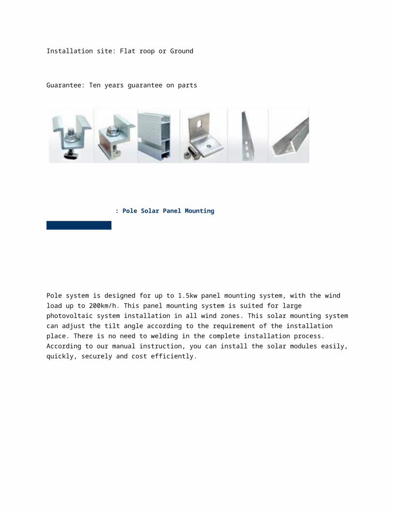
If necessary, use an angle grinder or hammer to cut a concavity in the tile that covers the roof hook at the point where the roof hook comes through. (Caution! Must not use fixed roof hook as a ladder, as this extreme point load could damage the tile below.
►Installation of the rails on roof hooks. Your rails consist of different length, always begin with the shortest piece. Install the rails on the roof hooks loosely at first, using T-screw.
►Installation of Clamps
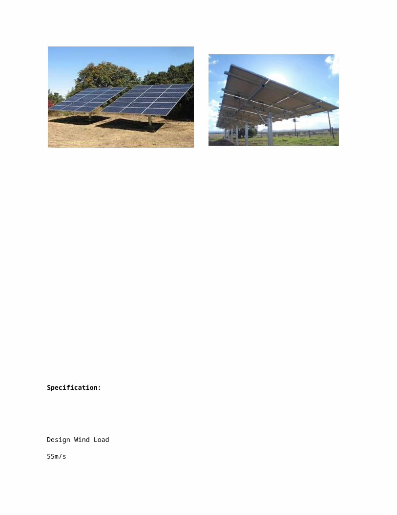
Installation of the splice to connect multiple rails together. Slide the splice on the rear side of the pre-assembled rails. Fasten the first bolt firmly. Then slide the next rail into the splice. When comes together, fasten the other bolt. The connection is finished. An expansion gap at the rail joints is suggested. Leave a gap about a finger width.
►Place the first module of the bottom row. Slide the end clamp tightly against the module and fasten it. Install the end clamp and mid clamps.
►Clamp Installation
►Slide the next module against the installed module. Fasten the mid clamp. Install other modules and clamps in this way. Keep module even.
In Our Project We connect Panel in both series and parallel.