Embed Size (px)
Citation preview

Institutionen för fysik, kemi och biologi
Examensarbete
Study of Radiation Damage of Lead Tungstate Crystals in
the Context of CMS ECAL
Daniel Edström
Examensarbetet utfört vid CERN
2011-04-07
LITH-IFM-A-EX-11/2404-SE
Linköpings universitet Institutionen för fysik, kemi och biologi
581 83 Linköping

Institutionen för fysik, kemi och biologi
Study of Radiation Damage of Lead Tungstate Crystals in
the Context of CMS ECAL
Daniel Edström
Examensarbetet utfört vid CERN
2011-04-07
Handledare:
Etiennette Auffray Hillemanns
CERN
Examinator:
Peter Münger
IFM, Linköpings universitet

Datum
Date
2011-04-07
Avdelning, institution Division, Department
Chemistry
Department of Physics, Chemistry and Biology
Linköping University
URL för elektronisk version
ISBN
ISRN: LITH-IFM-A-EX-11/2404-SE _________________________________________________________________
Serietitel och serienummer ISSN
Title of series, numbering ______________________________
Språk Language
Svenska/Swedish Engelska/English
________________
Rapporttyp Report category
Licentiatavhandling Examensarbete
C-uppsats
D-uppsats Övrig rapport
_____________
Titel
Title
Study of Radiation Damage of Lead Tungstate Crystals in the Context of CMS ECAL
Författare Author
Daniel Edström
Nyckelord Keyword
CERN, CMS, ECAL, Scintillator, Lead Tungstate, Radiation damage
Sammanfattning Abstract
The Large Hadron Collider, LHC, at CERN is capable of producing proton-proton collisions at a total energy of 14 TeV. Four principal detectors
are installed in the LHC to detect the various particles created in the collisions. In one of these detectors, the CMS, scintillating crystals of lead tungstate are utilized to convert the energy of electromagnetic particles to visible light. Due to the high amount of radiation in the detector, the
performance of the crystals may degrade during the lifetime of the detector.
In this work, crystals such as the ones used in the CMS detector are irradiated with gamma radiation and protons to estimate the transmission loss in the crystals. The spontaneous recovery at room temperature is studied over a period of several weeks. Induced diffusion is also studied. In addition,
techniques for reversing crystal damage are presented and studied. The techniques used are thermal bleaching, restoration by heating the crystals,
and optical bleaching, restoration by exposing the crystals to light of a specified wavelength. The light yield, the amount of light extracted per unit of deposited energy, for different crystals and different types of sources has also been
compared. The sources used have been gamma, alpha and neutron sources.
The induced absorption of standard PWO endcaps at 422 nm after being exposed to 1 kGy gammas was measured to be in the range of 0.6 to 0.7 m -
1. For mo-doped crystals the corresponding value was measured in the range of 0.2 to 0.3 m-1. When increasing the dose to 100 kGy the induced
absorption at 422 nm was found in the range of 1.17 to 1.32 m-1 for standard crystals and 3.02 to 4.43 m-1 for molybdenum doped crystals. The transmission could be completely recovered using thermal bleaching for both gamma and proton induced damage, while optical bleaching has so far
only been shown to perform a limited recovery. Proton irradiated samples demonstrated an induced diffusion, which could be eliminated using
thermal bleaching. The light yield of the measured crystals was shown to be consistently lower for alpha particles and neutrons than for gamma particles. The rates
varied in the range of 5% to 27% when comparing the light yield for alpha particles to gamma particles, and in the range of 5% to 70% when
comparing neutrons to gammas.

1
Study of Radiation Damage of Lead Tungstate Crystals in the Context of CMS ECAL Daniel Edström

2
Abstract The Large Hadron Collider, LHC, at CERN is capable of producing proton-proton collisions at a total
energy of 14 TeV. Four principal detectors are installed in the LHC to detect the various particles created
in the collisions. In one of these detectors, the CMS, scintillating crystals of lead tungstate are utilized to
convert the energy of electromagnetic particles to visible light. Due to the high amount of radiation in
the detector, the performance of the crystals may degrade during the lifetime of the detector.
In this work, crystals such as the ones used in the CMS detector are irradiated with gamma radiation and
protons to estimate the transmission loss in the crystals. The spontaneous recovery at room
temperature is studied over a period of several weeks. Induced diffusion is also studied. In addition,
techniques for reversing crystal damage are presented and studied. The techniques used are thermal
bleaching, restoration by heating the crystals, and optical bleaching, restoration by exposing the crystals
to light of a specified wavelength.
The light yield, the amount of light extracted per unit of deposited energy, for different crystals and
different types of sources has also been compared. The sources used have been gamma, alpha and
neutron sources.
The induced absorption of standard PWO endcaps at 422 nm after being exposed to 1 kGy gammas was
measured to be in the range of 0.6 to 0.7 m-1. For mo-doped crystals the corresponding value was
measured in the range of 0.2 to 0.3 m-1. When increasing the dose to 100 kGy the induced absorption at
422 nm was found in the range of 1.17 to 1.32 m-1 for standard crystals and 3.02 to 4.43 m-1 for
molybdenum doped crystals. The transmission could be completely recovered using thermal bleaching
for both gamma and proton induced damage, while optical bleaching has so far only been shown to
perform a limited recovery. Proton irradiated samples demonstrated an induced diffusion, which could
be eliminated using thermal bleaching.
The light yield of the measured crystals was shown to be consistently lowever for alpha particles and
neutrons than for gamma particles. The rates varied in the range of 5% to 27% when comparing the light
yield for alpha particles to gamma particles, and in the range of 5% to 70% when comparing neutrons to
gammas.

3
Sammanfattning LHC, “Large Hadron Collider”, är en partikelaccelerator vid CERN med en förmåga att producera
kollisioner mellan protoner och protoner vid 14 TeV total energi. Fyra huvuddetektorer är installerade i
LHC för att detektera de partiklar som skapas vid kollisionerna. I en av dessa detektorer, CMS, används
scintillationskristaller av bly-wolfram-oxid för att omvandla energin från elektromagnetiska partiklar till
synligt ljus. På grund av den stora mängden strålning i detektorn kan dessa kristallers egenskaper
försämras över tiden.
I detta arbete har kristaller av den typ som används i CMS-detektorn bestrålats med gammapartiklar och
protoner för att uppskatta förlusten av transmission i kristallerna. Den spontana återhämtningen av
transmission har studerats över en period av flera veckor. Inducerad diffusion från protoner har också
studerats. Tekniker för att återfå kristallernas egenskaper presenteras och deras effektivitet studeras.
Teknikerna som används är termisk blekning, återhämtning genom uppvärmning av kristallerna, och
optisk blekning, återhämtning genom att belysa kristallerna med ljus av en specifik våglängd.
Mängden ljus en kristall producerar per enhet av deponerad energi för olika kristaller och typer av källor
har studerats. De använda källorna har varit gamma-, alfa- och neutronkällor.
Den inducerade absorptionen hos standard endcap-kristaller vid 422 nm efter 1 kGy gammastrålning
uppmättes mellan 0,6 och 0,7 m-1. För molybdenium-dopade kristaller var det motsvarande värdet
mellan 0,2 och 0,3 m-1. Efter en dos av 100 kGy uppmättes den inducerade absorptionen mellan 1,17
och 1,32 m-1 för standardkristaller och mellan 3,02 och 4,43 m-1 för molybdenium-dopade kristaller.
Transmissionen kunde helt återfås medelst termisk blekning för både gamma- och protoninducerad
skada, medan optisk blekning hittills endast uppvisat delvis återhämtning. Protonbestrålade prov visade
en inducerad diffusion, som kunde elimineras med termisk blekning.
Mängden ljus de studerade kristallerna producerar visades vara konsekvent lägre för alfapartiklar och
neutroner än för gammapartiklar. Kvoten mellan mängden ljus producerat av alfapartiklar och
gammapartiklar varierade mellan 5 % och 27 % för de olika kristallerna. Motsvarande kvot för ljus
producerat av neutroner och gammapartiklar varierade mellan 5 % och 70 %.

4
Acknowledgements I would like to express my deepest appreciation to Etiennette Auffray Hillemanns, my supervisor at
CERN, for all her instruction and guidance during my time at CERN. I would also like to thank all the
people I have worked with during my time at CERN; Kristof Pauwels, Benjamin Frisch, Arno Knapitsch,
Stefan Gundacker, Georgios Mavromanolakis, Alain Machard, Igor Tarasov, Claire-Anne Reidel , Jean-
Philippe Torion-Hudry and Carl-Tommy Andersson. Finally I would like to thank my examiner at
Linköping University, Peter Münger, for his comments regarding this report and his patience while
waiting for me to finish my work.
Daniel Edström
Linköping, February 2011

5
Contents Chapter 1 Introduction ............................................................................................................................... 11
1.1 CERN ............................................................................................................................................ 11
1.1.1 LHC – The Large Hadron Collider ........................................................................................ 11
1.1.2 The CMS Experiment ........................................................................................................... 12
1.2 Scope of this Thesis ........................................................................................................................... 12
1.2.1 Problem Description and Objectives ......................................................................................... 12
1.2.2 Limitations .................................................................................................................................. 12
1.2.3 Outline of this Thesis .................................................................................................................. 13
Chapter 2 Background ................................................................................................................................ 14
2.1 The CMS Electromagnetic Calorimeter ............................................................................................. 14
2.1.1 Photodetectors .......................................................................................................................... 14
2.1.2 Preshower .................................................................................................................................. 15
2.1.3 Radiation environment .............................................................................................................. 15
2.2 Scintillation........................................................................................................................................ 17
2.2.1 Scintillation mechanism ............................................................................................................. 17
2.2.2 Luminescent centres .................................................................................................................. 18
2.2.3 Scintillation properties ............................................................................................................... 20
2.2.4 Creation of colour centres ......................................................................................................... 23
2.2.6 Recovery study ........................................................................................................................... 24
2.3 Lead Tungstate Crystals .................................................................................................................... 25
2.3.1 Crystal Production ...................................................................................................................... 25
2.3.2 Optical Properties ...................................................................................................................... 25
Chapter 3 Characterization of Crystals ....................................................................................................... 29
3.1 Transmission bench – The Spectrophotometer ................................................................................ 29
3.2 ACCOS ............................................................................................................................................... 31
Chapter 4 Results ........................................................................................................................................ 32
4.1 Gamma irradiation ............................................................................................................................ 32
4.1.1 Comparison between PWO and PWMO .................................................................................... 32
4.1.2 Thermal bleaching ...................................................................................................................... 38
4.1.3 Optical bleaching ........................................................................................................................ 39
4.2 Proton irradiation.............................................................................................................................. 41

6
4.2.1 Thermal Bleaching ...................................................................................................................... 44
4.2.3 Optical Bleaching ....................................................................................................................... 46
4.3 Diffusion ............................................................................................................................................ 47
4.4 Proton irradiation of standard endcaps ............................................................................................ 49
Chapter 5 Comparison of Light Yield for Different Sources ........................................................................ 52
5.1 Light Yield Measurements ................................................................................................................ 52
5.1.1 Classical Light Yield Bench 4 ....................................................................................................... 53
5.1.2 Extraction of Light Yield ............................................................................................................. 54
5.1.3 Light Yield for Different Sources ................................................................................................ 56
Chapter 6 Discussion and Conclusions ........................................................................................................ 60
6.1 Irradiation damage and recovery...................................................................................................... 60
6.1.1. Gamma Irradiation .................................................................................................................... 60
6.1.2 Proton Irradiation ...................................................................................................................... 61
6.2 Comparison of light yield for different sources ................................................................................ 61
6.3 Future work ....................................................................................................................................... 62
Bibliography ................................................................................................................................................ 63
7
Table of Figures Figure 1: Predicted radiation profile in inner detectors ............................................................................. 16
Figure 2: Fluence and absorbed dose behind crystals ................................................................................ 17
Figure 3: Energy diagram of a scintillator ................................................................................................... 19
Figure 4: Potential energy diagram for a luminescence centre .................................................................. 19
Figure 5: Theoretical and measured transmission of lead tungstate ......................................................... 27
Figure 6: Transmission and emission spectra of lead tungstate ................................................................. 28
Figure 7: Spectrophotometer ..................................................................................................................... 29
Figure 8: Transmission of standard and molybdenum doped endcaps ...................................................... 32
Figure 9: Pulse shape of standard and molybdenum doped endcaps ........................................................ 33
Figure 10: Induced absorption of standard and molybdenum doped endcaps after being exposed to 1
kGy gamma radiation. ................................................................................................................................. 34
Figure 11: Standard (left) and molybdenum doped (right) endaps after 100 kGy irradiation ................... 35
Figure 12: Induced absorption of standard and molybdenum doped endcaps after being exposed to 100
kGy gamma radiation. ................................................................................................................................. 35
Figure 13: Room temperature recovery of standard and molybdenum doped endcaps ........................... 36
Figure 14: Induced absorption of PWMO 129 ............................................................................................ 37
Figure 15: Room temperature recovery of PWMO 129 .............................................................................. 38
Figure 16: Thermal bleaching of standard and molybdenum doped endcaps. .......................................... 39
Figure 17: Optical bleaching setup.............................................................................................................. 40
Figure 18: Optical bleaching of standard and molybdenum doped endcaps ............................................. 40
Figure 19: Optical bleaching of PWMO 129 ................................................................................................ 41
Figure 20: Comparison of induced absorption after 1 kGy gamma irradiation of standard endcaps and
small samples .............................................................................................................................................. 42
Figure 21: Comparison of induced absorption after 100 kGy gamma radiation of standard endcap and
small sample ............................................................................................................................................... 43
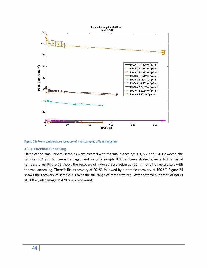
Figure 22: Room temperature recovery of small samples of lead tungstate ............................................. 44
Figure 23: Thermal bleaching of proton irradiated samples ...................................................................... 45
Figure 24: Thermal bleaching of proton irradiated sample 3.3 .................................................................. 46
Figure 25: Optical bleaching of proton irradiated sample 5.3 .................................................................... 47
Figure 26: Induced diffusion in proton irradiated samples. From top to bottom: Samples 5.1, 5.2, 5.3 and
5.4. From left to right: Before irradiation, top face after irradiation, side face after irradiation. .............. 48
Figure 27: Difference in collected light before and after irradiation .......................................................... 48
Figure 28: Recovery of diffusion with thermal bleaching in sample 3.3 .................................................... 49
Figure 29: Irradiation setup ........................................................................................................................ 49
Figure 30: Induced absorption of proton irradiated endcap crystals ......................................................... 50
Figure 31: Removed induced absorption after test beam period at 422 nm. ............................................ 51
Figure 32: Transmission of crystal 11128 before irradiation, after irradiation and after bleaching in test
beam. .......................................................................................................................................................... 51
Figure 33: Principle of a photomultiplier tube ............................................................................................ 53
Figure 34: Setup of bench 4 ........................................................................................................................ 53

8
Figure 35: Scintillation pulse of LYSO .......................................................................................................... 54
Figure 36: Scintillation spectrum of LYSO ................................................................................................... 55
Figure 37: Light yield spectrum of a LYSO crystal using a Co60 source ...................................................... 57
Figure 38: Light yield spectrum of an NaI crystal using an AmBe source ................................................... 57
Figure 39: Number of photoelectrons versus energy for NaI, CsI and LaBr3 using an AmBe source ......... 59

9
List of Tables Table 1: Sellmeier parameters for lead tungstate ...................................................................................... 26
Table 2: Light yield of standard and molybdenum doped endcaps ............................................................ 33
Table 3: Irradiation of small PWO samples ................................................................................................. 42
Table 4: Radioactive sources utilized for light yield measurements .......................................................... 56
Table 5: Summary of light yield measurements ......................................................................................... 58
Table 6: Trendlines for NaI, CsI and LaBr3 using an AmBe source ............................................................. 59

10
List of Abbreviations ALICE A Large Ion Collider Experiment ATLAS A Toroidal LHC ApperatuS BGO Bismuth germanate (Bi4Ge3O12) CERN European Organisation for Nuclear Research CMS Compact Muon Solenoid LHC Large Hadron Collider LHCb Large Hadron Collider beauty LHCf Large Hadron Collider forward LuYAP Lutetium Yttrium Aluminium Perovskite (Lu1-xYxAlO3) LY Light Yield LYSO Lutetium Yttrium OxyorthoSilicate (Lu2(1-x)Y2xSiO5) PMT PhotoMultiplier Tube PWO Lead Tungstate (PbWO4) QE Quantum Efficiency TOTEM TOTal Elastic and diffractive cross section Measurement

11
Chapter 1
Introduction
1.1 CERN CERN, the European Organization for Nuclear Research, is the world’s largest centre for particle physics.
It was founded in 1954 and is located on the border between France and Switzerland, near Geneva.
CERN is currently composed of 20 member states. Furthermore, several states and organizations,
including Russia, Japan, and the U.S.A, participate as observers. The main purpose of CERN is to provide
scientists with the necessary tools to study the basic constituents of matter and the forces binding them
together. To be able to study these building blocks of our universe, particles are accelerated in large
particle accelerators and then collided. CERN provides scientists from 580 institutes and universities all
over the world with access to accelerators, detectors, and computer centres for data processing.
Achievements at CERN include the discovery of the W and Z bosons which confirmed the unification of
the electromagnetic and weak interactions, the electroweak theory of the standard model. This
discovery led to the 1984 Nobel Prize for Simon van der Meer and Carlo Rubbia. The World Wide Web
was also first invented at CERN in 1989, in order to facilitate information sharing between scientists
across the globe.
1.1.1 LHC – The Large Hadron Collider
The most recent project at CERN is a circular collider called the LHC, the Large Hadron Collider. This
machine, located 50 to 175 meters beneath the outskirts of Geneva, possesses a circumference of 27
kilometers and will, at full capacity, provide collisions between two beams of protons or lead ions with
energy of 7 TeV each. In order to reach these energies, particles are accelerated in two separate beam
lines to a velocity of 99.99% of the speed of light. The beams are guided in the ring structure by
superconducting magnets cooled to a temperature of 1.9 K. The two beam lines intersect to form a
collision point at four different points in the tunnel. At each of these collision points a detector has been
constructed to observe the collisions and study the particles created. These detectors are: CMS, ATLAS,
LHCb, and ALICE. Two smaller detectors, TOTEM and LHCf, are located near the CMS and LHCf detectors
respectively, and will study the particles that pass each other closely rather than collide head on.
The purpose of the LHC is to attempt to further our understanding of the universe. This includes
searching for the Higgs boson, which may explain the origin of mass, investigating the nature of dark
matter, searching for extra spatial dimensions, recreating the conditions of the first few seconds of the
universe and the reason for the dominance of matter over antimatter.

12
1.1.2 The CMS Experiment
The CMS, Compact Muon Solenoid, Detector is located beneath the village of Cessy in France. More than
2000 scientists from 155 institutes in 37 countries work with the CMS experiment. The CMS detector is
designed as a general purpose detector and will observe a wide variety of particles and phenomena. The
detector is constructed in layers, where each layer is designed to detect a specific class of particles.
Going from the center and outwards, the first layer of the CMS detector is the tracking system. The
tracking system records the paths of charged particle, which reveal their momenta. The second layer is
the ECAL, the electromagnetic calorimeter. Consisting of scintillating crystals, this segment measures the
energies of electrons and photons. The third layer is the HCAL, the hadronic calorimeter, which
measures the energies of hadrons. The only known particles that may pass through the HCAL are the
muons and weak interacting particles such as neutrinos. Muons will be tracked in the next layer, a
dedicated muon tracking chamber. The neutrinos themselves may not be detected, but their presence
may be inferred by adding up the momenta of the detected particles and attributing any missing
momenta to the neutrinos. (1)
1.2 Scope of this Thesis This thesis aims to cover a final thesis project for a Master of Science in Applied Physics and Electrical
Engineering at Linköping University at the Department of Physics, Chemistry and Biology. The work has
been carried out at CERN in Meyrin, Geneva, under the supervision of Etiennette Auffray Hillemanns.
The work commenced the first of March, 2010, and ended the 21st of December, 2010.
1.2.1 Problem Description and Objectives
The CMS electromagnetic calorimeter consists of over 70 000 scintillating lead tungstate crystals. The
crystals emit light when exposed to ionizing radiation. The amount of light emitted is proportional to the
energy absorbed from the radiation. This relationship enables the crystals to function as particle
detectors. During the operation of the LHC the crystals will be exposed to large amounts of radiation.
The exposure will over time create damages in the crystal, resulting in induced absorption and the
subsequent loss of crystal transmission and light output. In order to prepare for the years to come, it is
important to understand what amount of damage can be expected to occur in the crystals and if it is
possible to recover from it. The aim of this thesis is to study the effect of radiation damage on the same
type of crystals as those used in the CMS electromagnetic calorimeter. Both gamma irradiation and
proton irradiation are studied. Techniques to recover from radiation damage are also presented and
their efficiency measured. As a supplementary study, the light yield for various crystals from different
kinds of particles has been studied and compared.
1.2.2 Limitations
The radiation absorbed by the lead tungstate crystals in the CMS electromagnetic calorimeter is
expected to take place over the span of ten years. It is of course not possible to irradiate the crystals
studied in this thesis for the same amount of time, and so the crystals studied in this work are instead
irradiated over the course of several days.

13
1.2.3 Outline of this Thesis
The CMS electromagnetic calorimeter which the lead tungstate crystals are used in is a large and
complex technical system, and as such requires a detailed introduction to be understood. This
introduction is presented in chapter two. This chapter also serves to detail the mechanisms of
scintillation. Important properties of scintillators are presented and described. The production methods
and scintillation properties of lead tungstate are also presented. Chapter three details the mechanisms
of damage recovery in scintillating crystals and presents the measurements apparatuses used in the
recovery study. Chapter four presents the result of the recovery study for different types of radiation
and recovery treatments. Chapter five outlines the light yield measurements when using different
sources. Finally, chapter six provides discussion and conclusion for the work presented.

14
Chapter 2
Background
2.1 The CMS Electromagnetic Calorimeter The purpose of the CMS Electromagnetic Calorimeter (ECAL) is to measure the energies of electrons,
positrons and photons created in particle collisions. It will also contribute to the measurement of
hadrons and missing energies in collaboration with the Hadron Calorimeter. In the search for the Higgs
Boson, the ECAL will be instrumental through the measurement of the two-photon decay mode for mH ≤
150 GeV and the measurement of the electrons and positrons from the decay of the W- and Z-bosons
originating in the H → ZZ(*) and H→WW decay chain for 140 GeV ≤ mH ≤ 700 GeV. Measuring these
phenomena requires excellent energy resolution and angular resolution. Further requirements are a fast
response time and high resistance to radiation, due to operating conditions of the LHC. (2) The ECAL is
composed of a central barrel part enclosed by two endcap parts, one at each end of the barrel. The
barrel contains 61200 lead tungstate (PbWO4) crystals, and the endcaps 7324 crystals each. Lead
tungstate was chosen because of its properties making the crystals well suited to the CMS environment.
Lead tungstate has a short radiation length and small Moliere radius, which enables a compact
calorimeter. Furthermore, it has a fast response and is relatively easy to produce. The barrel crystals are
arranged in submodules of ten crystals each and placed in an alveolar structure. These submodules are
then arranged in modules of 40 or 50 submodules. Three modules of 40 and one module of 50
submodules make up one supermodule of which there are a total of 36. The barrel crystals measure 230
mm in length and have a cross-section of around 22*22 mm2. The exact shape of the crystal varies with
their position in the barrel. The endcap crystals are arranged in supercrystals of 25 crystals. Each endcap
consists of 276 standard supercrystals in addition to 36 partial supercrystals. All crystals in the endcap
have the same size and shape. They are 220 mm long, the rear face 30*30 mm2 and the front face
28.6*28.6 mm2. (3)
2.1.1 Photodetectors
The photodetectors used in the ECAL have several requirements placed on them. First of all, the PbWO4
crystals have a relatively low light yield, so they must have a high gain. Furthermore, they must be able
to withstand both the high magnetic field and harsh radiation environment of the detector. Finally, they
must have a fast response. With these requirements in mind, silicon Avalanche Photodiodes (APDs) are
used in the barrel and Vacuum Phototriodes (VPTs) in the endcaps. For the barrel, two APDs are glued to
the back of each crystal, covering 50 mm2 of the surface. The gain of the APDs is 50 and the quantum
efficiency ≈80% for PWO crystals. The APDs cannot be used in the endcaps because they are not
sufficiently radiation hard. Instead, VPTs are used. The gain of the VPTs is close to 10 and their quantum
efficiency ≈15% (3)

15
2.1.2 Preshower
The main purpose of the preshower detectors is to distinguish neutral pions from photons in the
endcaps. They are situated in front of the endcap crystals and consist of layers of lead converters
followed by detector planes of silicon strips. (3) In order to correct for the energy deposited in the lead
converter, the energy measured in the silicon is used to apply corrections to the measurements in the
crystals.
2.1.3 Radiation environment
The nominal luminosity of the LHC is 1034 cm-2s-1. Together with the beam energy of 7 TeV it will create a
very hostile radiation environment. This can result in radiation damage in both the scintillating crystals
and the electronic components. There is also the effect of induced radioactivity to be considered, which
aside from being a safety issue may increase the level of background noise in the detectors. When
discussing radiation, there are some units that need to be defined. Flux is the number of particles
crossing a unit surface per unit of time. Fluence is the time integral of the flux; it is usually expressed in
number of particles*cm-2. Absorbed dose is the amount of energy deposited in a material per unit of
mass. It is expressed in Gy. While particle fluence and absorbed dose are correlated for a given particle
type, energy, and medium, they should not be treated as synonyms. (2)
Pseudorapidity is a spatial coordinate which describes the angle of a particle relative to the beam. It is
defined as
𝜂 = −ln[tan(
𝜃
2)]
(2.1)
where θ is the angle relative to the beam.
Figure 1 shows the predicted dose profiles for the inner detectors of CMS for 500 fb-1 and 2500 fb-1
respectively. These values correspond to the end of year 2020 and 2028.
Figure 2 shows the predicted neutron and charged hadron fluence and absorbed dose immediately
behind the crystals as a function of pseudorapidity. The values given correspond to 500 fb-1.

16
Figure 1: Predicted radiation profile in inner detectors. (4) The upper graph shows the predicted dose distribution for 500 fb-1
and the lower graph for 2500 fb
-1.

17
Figure 2: Fluence and absorbed dose behind crystals. (2) The upper graphs show the predicted particle fluence directly behind the crystals as a function of pseudorapidity. The lower graphs show the corresponding predicted dose. The left graphs are for the barrel and the right graphs are for the endcap.
2.2 Scintillation The defining property of a scintillator is the ability to absorb ionizing radiation (alpha, gamma, beta and
X-ray) and reemit the energy in the form of visible light. Depending on the time taken for the emission,
the scintillation can be divided into two categories. If the light is emitted with 10-8 seconds, which is
roughly the time of atomic transitions, of the absorption the process is called fluorescence. If the process
takes more time than this it is called phosphorescence, or afterglow. The time delay between the
absorption and the emission is due to a metastable excitation state. Depending on the material, this
delay can vary from a few microseconds to hours.
2.2.1 Scintillation mechanism
When a scintillator absorbs radiation it is excited into a non-equilibrium state. From this state, the
scintillator will relax into equilibrium and emit light in the process. It is this process which is called
scintillation. This relaxation occurs via several processes, but can be divided into five principal steps. (4)
1. The absorption of ionizing radiation causes the creation of primary holes and electrons.

18
2. The primary holes and electrons relax through the creation of secondary holes and electrons,
photons, plasmons and other electric excitations.
3. Thermalization of low-energy electron-hole pairs results in a number of electron-hole pairs with
energy just above the band gap energy Eg.
4. Energy is transferred from the electron-hole pairs to the luminescent centres and their
excitations.
5. The luminescent centres are deexcited via the emission of light.
The first three steps in this process are similar for all condensed matter. It is the second of these steps
that is the most complex. The primary electron creates an electromagnetic cascade in the material
consisting of electrons, holes, photons and plasmons. The number of these secondary particles increases
with the depth of the cascade. The creation of secondary particles increases until the electromagnetic
particles are unable to further ionize the material. At this stage the electron-hole pairs relax thermally to
energy positions near the band gap energy. From this electromagnetic cascade some important
parameters may be defined. One of these is the radiation length, X0, which is defined as the mean
distance travelled by an electron until its energy has been decreased by a factor 1/e. Another important
parameter for scintillators is the Moliere radius, RM, which can be understood as the radius of an infinite
cylinder containing 90% of the shower energy. The last two steps in the scintillation process are
characteristic for different materials due to the involvement of the luminescent centres. These centres
are the cause of the light emission and therefore most properties of the scintillation are caused by them.
2.2.2 Luminescent centres
The light emitted by a scintillator originates from radiative transitions between electronic levels which
are called luminescent centres. The luminescent centres can either be intrinsic, meaning they originate
from the crystal itself, or extrinsic, if their presence is due to impurities present in the crystal. In order to
understand the mechanism of scintillation, we may employ the band theory. From this theory, we learn
that the electrons of a completely free atom will occupy discrete energy levels given by Schrödinger’s
equation. When atoms are brought together to form a solid, these energy levels will form a continuum
of allowed energy levels, so called energy bands that the electrons may occupy. In between these bands
are forbidden energy levels that the electrons may not occupy, so called energy gaps. In the normal
state, the higher energy bands of the material are empty and the lower energy bands are filled with
electrons. The filled band of the highest energy is called the valence band, and the empty band of the
lowest energy is known as the conduction band. The valence band and the conduction band is separated
by an energy gap known as the bandgap, Eg. However, this model is only true for an insulator with a
perfect crystal structure. In a real scintillator there are defects and impurities in the crystal lattice which
give rise to local energy levels within the band gap which electrons may occupy. These levels may be
characterized as three different types.
Luminescent centres, from where the electron is relaxed via the emission of light.
Quenching centres, from where the relaxation is achieved through thermal dissipation.
Traps, a metastable level from where an electron may either gain energy from lattice vibrations
and pass to the conduction band or lose energy and fall to the valence band.

19
The luminescent and quenching centres are caused by interstitial ions, impurities or defects. They
introduce local energy states corresponding to the ground and excited state of the centre. Traps arise
from other lattice defects and introduced energy levels below the conduction band.
Figure 3: Energy diagram of a scintillator. (5) The left picture shows the energy diagram of an insulator with a perfect crystal lattice. The right picture shows the energy diagram of a scintillator with quenching and luminescence centres and traps.
Mechanism for the luminescence of a centre
The mechanism of luminescence can be discussed using a theoretical model applicable to all
luminescent materials. In this model, the potential energies of the ground and excited states of the
luminescent centre are plotted against a configurational coordinate, the mean inter-atomic distance
between the luminescent centre and its neighbouring atoms. Figure 4 is an example of such a plot.
Figure 4: Potential energy diagram for a luminescence centre. (5) The lines F1 and F2 correspond to the ground and excited states of the centre. The arrows A-C and B-D depict the excitation de-excitation processes.
In Figure 4 the minima A and B correspond to the stable energy positions of the ground and excited
states, respectively. When the luminescence centre is excited, there is a transition from point A to point
C. The transition is vertical in the configuration diagram because it is fast compared to the speed of
atomic movements in the crystal. (3) In position C, the centre is not in its energy minimum and so it

20
moves to position B. The energy lost in the move is disposed of through thermal dissipation. The centre
will remain in position B for a time that depends on the probability of an optical transition. This optical
transition is what causes the emission of light. The optical transmission is vertical in the configuration
diagram, again because of the speed of the emission in relation to the speed of atomic movements.
Once in position D, the centre will move to position A by means of thermal dissipation. One may note
that the emission occurs at lower energies than the absorption. This is what is known as Stokes’ Law,
and the difference is expressed as the Stokes shift λem-λex where λem is the wavelength of the emission
and λex the wavelength of the excitation. A large Stokes shift indicates strong coupling between
electrons and phonons. (6) The potential energy curves of the ground and excited states typically
approach or intersect each other at some point. In Figure 4 this is point F. An excited luminescence
centre in point F can make a non-radiative transition to point F1 and from there dissipate the excess
energy thermally. The probability of this process increases with temperature, as vibrational states closer
to F may be occupied. This process is known as internal thermal quenching and competes with the
scintillation process.
Luminescence centres of Lead Tungstate
PbWO4 crystals have been shown to have three luminescent bands. (3)
A blue band at 420 nm. This is present in all tungstates, which suggests it is caused by 𝑾𝑶𝟒𝟐−
centres.
A green band at 490 nm. When anion vacancies are present in the 𝑾𝑶𝟒𝟐− centres irregular
anionic 𝑾𝑶𝟑 molecular complexes form, causing this band.
A red band at 650 nm. This band is also caused by irregular 𝑾𝑶𝟑 centres, in this case deformed
by Frenkel defects.
The luminescence spectrum of lead tungstate is the result of the combination of these three bands.
However, the red and green centres are primarily related to slow components of the emission and are
thus not desirable. For this reason these centres have been suppressed by means of special doping,
resulting in an emission spectrum peaking at 420 nm.
2.2.3 Scintillation properties
Light Yield
The light yield is perhaps the most fundamental property of a scintillator. It is defined as the number of
photons emitted by the scintillator per unit of deposited energy, typically MeV. When measuring the
light yield, gamma sources are typically used.
𝑳𝒀 =𝒏𝒑𝒉
𝑬𝜸 (2.2)
In this equation, 𝒏𝒑𝒉 is the number of emitted photons and 𝑬𝜸 is the energy of an incident gamma
particle. The number of photons can be rewritten as
𝒏𝒑𝒉 = 𝒏𝒆−𝒉𝑺𝑸, 𝟎 < 𝑆, 𝑄 < 1
(2.3)

21
Here, 𝒏𝒆−𝒉 is the number of electron-hole pairs created by the incident radiation. S is the efficiency of
the energy transfer from the electron-hole pairs to the luminescence centres and Q is the efficiency of
the energy transfer from the luminescence centre to emitted light. The energy required to create an
electron-hole pair can be written as
𝑬𝒆−𝒉 = 𝑩𝑬𝒈
(2.4)
where 𝑬𝒈 is the bandgap and 𝑩 is a material constant. Utilizing this relation, the number of electron-
hole pairs created may be written as
𝒏𝒆−𝒉 =
𝑬𝜸
𝑩𝑬𝒈
(2.5)
Inserting this into our original equation thus yields
𝑳𝒀 =
𝑺𝑸
𝑩𝑬𝒈
(2.6)
With this relation, we may estimate the maximum theoretical light yield of PbWO4 by setting S=Q=1. The
band gap of PbWO4 is 𝑬𝒈 = 𝟒. 𝟓 eV and it is known that 𝑩 ≈ 7 for tungstates. Inserting these values
yield an estimation of 𝑳𝒀𝒎𝒂𝒙 ≈ 𝟑𝟐 𝟎𝟎𝟎 ph/MeV. In reality, the observed light yield for these crystals is
closer to 𝑳𝒀 ≈ 100 ph/MeV. The large difference in the theoretical maximum and measured values is
due to the strong thermal quenching present in PbWO4, resulting in a Q << 1. (5)
Decay time
A scintillator’s decay time describes the amount of light emitted after a certain time. It is defined as the
time after which the amount of light emitted has decayed to 1/e of its initial value.
The light intensity as a function of time can be expressed using a sum of exponential functions. (3)
𝑰 𝒕 = 𝑨𝒊𝒆
−𝒕𝝉𝒊
𝒏
𝒊=𝟏
(2.7)
Here 𝑨𝒊 and τi are the initial intensity and decay time of component i, respectively, and n the number of
components. This model accurately describes the intensity when one component is used for each
luminescence centre in the scintillator. From this model, we may also define the contribution from each
component, Ci, and the mean decay time, τm. The parameter Ci is usually given as a percentage.
𝑪𝒊 =
𝑨𝒊𝝉𝒊
𝑨𝒋𝝉𝒋𝒏𝒋=𝟏
(2.8)
𝝉𝒎 =
𝑨𝒏𝒊=𝟏 𝒊
𝝉𝒊𝟐
𝑨𝒊𝝉𝒊𝒏𝒊=𝟏
(2.9)

22
The decay time is related to the mean lifetime of the excited states and therefore inversely proportional
to the probability of de-excitation. The de-excitation can be either radiative or non-radiative, yielding
𝝉 ∝
𝟏
𝑷𝒓 + 𝑷𝒏𝒓
(2.10)
Similarly, we define the luminescence efficiency η as the ratio between the probability of a radiative
de-excitation and the total probability of de-excitation.
𝜼 ∝
𝑷𝒓
𝑷𝒓 + 𝑷𝒏𝒓
(2.11)
Looking at these two equations, we see that the luminescence efficiency and the decay time are at odds.
Increasing 𝑷𝒏𝒓 leads to a decreased decay time, and thus a faster response, but also decreases the
efficiency which leads to a weaker emission.
Radiation Hardness
Radiation damage will always occur when ionizing radiation interacts with scintillation crystals. The
creation of damage is a complex process depending not only on the material but also on defects and
impurities in the crystal. Defects such as this increase the probability of the formation of radiation
induced colour centres or point defects within the crystal. Changes in optical or scintillation properties
of a crystal can be caused during irradiation or after the accumulation of large doses. The properties of
the crystal can be impaired in several ways. (4)
Formation of colour centre absorption bands which absorb the photons emitted by the
luminescence centres, causing a decrease of the optical transmission. This is especially harmful
in large gamma detectors for high energy physics.
Direct effect on the emission characteristics. The luminescence centres may be quenched
because of valence changes or ion diffusion. There may also be a reduction of the amount of
emitted light due to reduction of energy transfers from electrons or holes to luminescence
centres. The carrier mobility is reduced by the radiation induced defects and traps.
Created shallow traps increase the amount of afterglow.
Heavy crystals irradiated by high energy hadrons display induced radioactivity which can
influence the operation of electromagnetic calorimeters.
A large amount of research shows that a loss of transmission is the most significant effect of radiation
damage. For most crystals an observed loss in light yield can be explained by loss of transmission rather
than luminescence. For this reason, the transmission is the primary property studied in radiation
hardness studies. (7) Certain crystals may recover their transmission with time. The recovery at room
temperature is often very slow, however. By means of thermal bleaching at an elevated temperature it
is possible to obtain almost complete recovery. The temperature and time required depend on the
properties of the colour centres. Another, more subtle, way of recovering radiation damage is by optical
bleaching. This technique entails illuminating the damaged crystal with UV or visible light. If this
technique can be demonstrated to work for the lead tungstate crystals, this provides an important tool

23
to deal with radiation damage inside the actual detector by bleaching the crystals during the periods
when the detector is not operating. If the wavelength and intensity of the light is carefully selected it
should be possible to fully recover the crystal transmission.
2.2.4 Creation of colour centres
When a crystal is exposed to ionizing radiation, the electrons are lifted from the valence band to the
conduction band where they are free to travel in the crystal. The holes created in the valence band
when the electrons are excited may also migrate. If the electrons or holes encounter a crystalline defect
they may be trapped. The most studied case is the case of an electron trapped by a negative ion
vacancy, which may be considered as an electron bound to a positive centre. A system like this generally
possesses a spectrum of energy levels. Excitation between these levels produces a series of optical
absorption lines analogous to those found in an isolated atom. (8) These centres are known as F-centres,
from the German word ‘Farbe’, colour. F-centres may be arranged in groups. Two neighbouring
vacancies trapping two electrons constitute an M-centre. Three neighbouring vacancies trapping three
electrons are known as an R-centre. One vacancy trapping two electrons is known as an F’-centre. Holes
are generally trapped by other defects than vacancies. A Vk-centre consists of a hole trapped between
two neighbouring negative ions. This centre possesses an absorption spectrum similar to that of Cl2. The
introduction of impurities surrounding an F-centre generates a new family of colour centres. The most
well-known, the FA-centre is the result of the substitution of one of the six positive ions closest to an F-
centre for an impurity. The reduction of symmetry of the centre induces a new absorption spectrum. (8)
2.2.5 Definition of induced absorption
The irradiation of crystals creates colour centres which modify the absorption of the crystal. This effect
is caused by the energy levels associated with the defects, which causes a supplementary absorption.
We may thus write the absorption of the crystal, μ, as a sum of the intrinsic absorption, μi, and the
induced absorption created by the colour centres, μind. (7)
𝜇 = 𝜇𝑖 + 𝜇𝑖𝑛𝑑
(2.12)
The transmission of the crystal after irradiation is given by
𝑇𝑖𝑟𝑟 = 𝑇𝑡𝑒−𝜇𝐿 (2.13) where Tth is the theoretical transmission.
𝑇𝑖𝑟𝑟 = 𝑇𝑡𝑒−𝜇 𝑖𝐿𝑒−𝜇 𝑖𝑛𝑑 𝐿
(2.14)
𝑇𝑖𝑟𝑟 = 𝑇𝑖𝑒−𝜇 𝑖𝑛𝑑 𝐿
(2.15)
where Ti is the initial transmission. From this expression we may deduce the expression for the induced
absorption.

24
𝜇𝑖𝑛𝑑 =
1
𝐿ln(
𝑇𝑖
𝑇𝑖𝑟𝑟)
(2.16)
When studying the effect of radiation damage and its recovery, the induced absorption is the quantity
studied.
2.2.6 Recovery study
A number of studies of the radiation hardness of different materials have revealed that the colour
centres created by irradiation are not always stable. As time passes, a decrease of the induced
absorption can be observed in some cases. This recovery can be achieved at room temperature, but it is
facilitated by increased temperature. It is also possible to observe this recovery when the crystal is
illuminated by light. In this case we speak of optical recovery. (7)
Examples of recovery mechanisms
For instance, consider the simple case of an F centre, an electron trapped in an anion gap. We let P be
the probability of the release of the electron from the trap and n(t) the density of F centres at the
moment t. In the case of direct recombination, the evolution of the density of F centres, at a given
temperature, is governed by the following differential equation (7):
−
𝑑𝑛
𝑑𝑡= 𝑃 ∗ 𝑛(𝑡)
(2.17)
The solution to this equation is
𝑛 𝑡 = 𝑛0𝑒−𝑃𝑡
(2.18)
where n0 is the initial density of created colour centres. Because the absorption associated with colour
centres is proportional to their density, there will be an exponential decrease of the absorption caused
by the colour centres. If there is not direct recombination of the electron, the differential equation is
not of the first order, and the recovery process will be slower. It is also interesting to study how the
recovery changes with temperature. The probability of recovery P of a centre is given by Boltzmann’s
law:
𝑃 = 𝐴𝑒
−𝐸𝑘𝑇
(2.19)
where A is a proportionality constant and E is the thermal deactivation energy. The higher this energy is,
the harder it is for an electron or hole to escape a trap. In this case the damage is stable at ambient
temperature. It is necessary to heat the crystal to a temperature so that E < kT to observe a recovery. If
the recovery with temperature is accompanied by an emission of light, it is known as
thermoluminescence.

25
2.3 Lead Tungstate Crystals
2.3.1 Crystal Production
The lead tungstate crystals for the CMS ECAL are produced at two different locations: Bogoroditsk
Techno-Chemical Plant (BTCP) in the Tula region, Russia, and Shanghai Institute of Ceramics (SIC) in
Shanghai, China. They are grown from a mixture of equal amounts of lead oxide (PbO) and tungsten
oxide (WO3). The crystals are grown using two different procedures. At BTCP the Czochralski method is
used, and at SIC the Bridgman-Stockbarger method is used.
In the Czochralski method, named after its inventor Jan Czochralski, the raw materials are melted in a
crucible. A seed crystal is then attached to a vertical arm so that it is just in contact with the surface of
the melt. The arm then slowly pulls the seed upwards, causing the melt to crystallize at the phase
boundary. By rotating the crystal slowly it is possible to avoid replicating inhomogeneities of the melt in
the crystal. Because the temperature, pulling speed and rotational speed influences the properties of
the crystal, it is important they are kept constant. (6) An advantage of this method is that if the seed has
an oriented crystal structure the grown crystal will have the same.
In the Bridgman-Stockbarger the crystal is grown inside a sealed container, the ampoule. The ampoule is
slowly lowered from a hot zone, where the materials are melted, into a cold zone where the
crystallization takes place. In order to control the growing conditions the hot and cold zones are heated
separately. (6) The advantage of this method is that nearly all of the raw materials are used to form the
crystal. A drawback is that some of the material may adhere to the walls of the ampoule, causing
stresses which reduce the crystal quality.
2.3.2 Optical Properties
Theoretical Transmission
Transmission describes how much of the light entering the crystal at one side exits at the other side.
PbWO4 is an optically anisotropic medium of uniaxial type. This means that inside the crystal there will
be both an ordinary ray, travelling according to the laws of isotropic media, and an extraordinary ray
which travels with a velocity depending on the angle between the crystal optical axis and the interface
between the crystal and the surrounding air. Because of this, the material has two indexes of refraction,
the ordinary and an extraordinary index. An estimation of the transmission can nevertheless be
obtained by considering the crystal as an isotropic medium. The complex index of refraction is N=n-ik.
From this, we may define the reflectance and absorption coefficient of a material.
𝒓 𝝀 =
𝑵 𝝀 − 𝟏
𝑵 𝝀 + 𝟏
𝟐
(2.20)

26
𝜶 𝝀 =
𝟒𝝅𝒌(𝝀)
𝝀
(2.21)
In general, the transmission of a material is a function of these parameters and the thickness d of the
material.
𝑻(𝝀) =
(𝟏 − 𝒓)𝟐𝒆−𝜶𝒅
𝟏 − 𝒓𝟐𝒆−𝟐𝜶𝒅
(2.22)
Assuming that a perfect crystal only suffers transmission losses from reflections, we set 𝜶 𝝀 = 𝟎 and as
such 𝒌 𝝀 = 𝟎. The consequences for our equations are as follows.
𝑻(𝝀) =
(𝟏 − 𝒓)𝟐
𝟏 − 𝒓𝟐
(2.23)
𝒓 𝝀 =
𝒏 𝝀 − 𝟏
𝒏 𝝀 + 𝟏
𝟐
(2.24)
In order to find the refractive index n(λ) it is possible to use Sellmeier’s law, as formulated below.
𝒏𝟐 − 𝟏 =
𝒏𝒔𝒊𝟐
𝟏 − (𝝀𝒔𝒊
𝝀)𝟐
𝒎
𝒊=𝟏
(2.25)
where 𝒏𝒔𝒊𝟐 and 𝝀𝒔𝒊
are the intensities and wavelengths of the optical resonances in the material. For lead
tungstate, in the range of 320-850 nm, it is adequate to use a constant term for short wavelength
resonances and one resonance term for the ultraviolet range. Sellmeier’s law thus becomes
𝒏𝒐𝒓𝒅
𝟐 − 𝟏 = 𝒏𝒔𝟎𝟐 +
𝒏𝒔𝟏𝟐
𝟏 − (𝝀𝒔𝟏
𝝀)𝟐
(2.26)
The appropriate values for the parameters are expressed in the table below. (3)
ns0 ns1 λs1
1.5821±0.0080 1.1062±0.0097 270.63±0.82 nm Table 1: Sellmeier parameters for lead tungstate
Using these parameters and the above equation, nord may be calculated. This may then be inserted into
the expression for reflectance, which may in turn be inserted into the expression for transmission.

27
Figure 5: Theoretical and measured transmission of lead tungstate asa function of wavelength. The circled line shows the calculated theoretical transmission for an isotropic crystal without absorption. The dotted line shows the measured transmission.
This calculation is valid for an isotropic crystal without absorption. As described earlier this assumption
is false for lead tungstate. A measured transmission spectrum for lead tungstate is displayed in Figure 5,
together with the calculated spectrum. As seen in the figure, the curves agree with each other for
λ ≥ 450. For λ ≤ 350 nm there is, however, a large disagreement. The reason for this disagreement is the
assumption that there is no absorption. Within the band model, light with energy above that of the
band gap will be absorbed to lift an electron from the valence band to the conduction band. The band
gap of lead tungstate is 4.5 eV, or 275 nm. (3) The theoretical curve agrees with this consideration.
However, a real crystal will also display internal absorption, which mostly occurs in the UV range. This
internal absorption is the reason for the shift of the band edge in the real spectrum compared to the
theoretical model. It is important for a scintillator that the transmission is as high as possible at the
position of the emission peak, so that the crystal does not reabsorb the light emitted by the scintillation
process. The emission spectrum of lead tungstate is shown together with the transmission in Figure 6.

28
Figure 6: Transmission and emission spectra of lead tungstate (3). The bold line shows the typical transmission spectrum for a lead tungstate crystal expressed as a percentage. The thin line shows the emission intensity in arbitrary units.

29
Chapter 3
Characterization of Crystals
3.1 Transmission bench – The Spectrophotometer The purpose of the transmission bench is to compare the amount of light entering a crystal with the
amount of light exiting it. This is done in order to find the light transmission as a function of wavelength.
The main components of this transmission bench are a 150 W Xenon lamp, a monochromator, and a
photomultiplier tube serving as a detector. The light emitted by the xenon lamp is focused at the
monochromator and a set of filters located at the end of the monochromator serves to eliminate higher
order diffractions.
Figure 7: Schematic diagram of the spectrophotometer.
The components of the spectrophotometer are as follows:
A 150 W Xenon lamp emitting in the range of 200 to 700 nm.
Several ultraviolet lenses to focus the light emitted by the lamp into the monochromator, and to
collimate the light exiting the monochromator.
Monochromator
Filters
PMT
PC
Electronics
Mirror
Chopper
Crystal
White box
DiaphragmBeamsplitter
Lens LensXenonLamp

30
A monochromator to select a specific wavelength. A motor coupled to the monochromator
provides for automatic scanning of a given wavelength region
A number of filters to eliminate higher order diffractions from the monochromator. A stepping
motor selects the filter to be used depending on the wavelength of the monochromator.
A beam splitter that separates the light beam into two different beams, one traversing the
crystal that is measured and one used as a reference.
A chopper to alternate between the two beams. In order to make a correct measurement, the
chopper must rotate with a frequency between 11 and 21 Hz. Should the chopper frequency
drift outside of this range, an error is produced.
A white box to defuse the light and make it arrive uniformly at the photomultiplier. This is
because the measured signal depends on the impact position of the light on the photomultiplier
cathode.
A photomultiplier that measures the incident light.
A moving table driven by a motor. Using this table several crystals can be measured without
manually changing the crystal between each measurement.
A LabVIEW program that controls the different parts of the machine and calculates the
transmission coefficient from the measured light.
When performing a measurement, the signal from the photomultiplier is measured 25 times for each
beam for every wavelength. From this data, the LabVIEW program calculates K, defined as
K(λ) =
< 𝑀 >
< 𝑅 >
(3.1)
Here, <M> is the average signal from the crystal beam, the beam passing through the crystal, and <R>
the average signal from the reference beam. This value does not depend on variations of the lamp or
the photomultiplier. However, because the mirror reflectivity and beam splitter separations are
functions of lambda, there will be some differences between the crystal beam and the reference beam.
To compensate for this, a reference measurement without a crystal is performed every morning. This
measurement is used to separate the signal differences caused by properties of the crystal being
measured from those induced by wavelength dependencies of the equipment. For a reference
measurement, the above equation becomes as follows:
𝐾𝑟𝑒𝑓 =
< 𝑀𝑟𝑒𝑓 >
< 𝑅𝑟𝑒𝑓 >
(3.2)
The final transmission can then be written as
𝑇 𝜆 =
𝐾(𝜆)
𝐾𝑟𝑒𝑓 (𝜆)
(3.3)
31
Because fluctuations in the power supply, lamp, detector and other irregularities are automatically
compensated, these measurements are very stable. (3)
3.2 ACCOS ACCOS stands for Automatic Crystal Control System. This system enables measurement of several
crystals with minimal manual operation. The specific machine used for this work is called ACCoCE 2 and
is installed at CERN. Up to 30 crystals can be loaded unto ACCoCE 2. This is done by means of a special
loading system, so that the crystals need not be placed manually. The machine is capable of measuring
longitudinal transmission, transversal transmission, light yield and the dimensions of a crystal. (3)
Transversal transmission and light yield can be measured at several points along the length of the
crystal.

32
Chapter 4
Results
4.1 Gamma irradiation
4.1.1 Comparison between PWO and PWMO
It has been speculated that doping PWO with molybdenum will increase its radiation hardness. To
investigate this, both standard PWO crystals and molybdenum doped (PWMO) crystals have been
irradiated with gamma rays.
Figure 8: Transmission of standard and molybdenum doped endcaps. The blue lines correspond to standard PWO crystals, while the red lines correspond to Mo-doped crystals.
Figure 8 shows the typical transmission spectra for two standard endcap crystals and three PWMO
crystals. A distinct shift in the band edge in the PWMO crystals can be observed. This shift is in the order
of 30 nm. Aside from this shift, the spectra are very similar. Scintillation properties are summarised in
table 1 and Figure 9. The molybdenum doped crystals clearly have a higher light yield, at the cost of a
slower response.

33
Crystal ID Ly at 8Xo (pe/MeV)
Standard PWO Crystal 10.5
3011 15.3
3012 15.8
3013 15
3014 16.5
Table 2: Light yield of standard and molybdenum doped endcaps expressed in PE/MeV. Crystals 3011 to 3014 are doped with Mo.
Figure 9: Pulse shape of standard and molybdenum doped endcaps. The blue curve shows the scintillation pulse from a standard PWO crystal. The green curve shows the scintillation pulse from a Mo-doped PWO crystal. Measurement performed by E. Auffrray.

34
Two standard PWO crystals and three molybdenum doped crystals were irradiated with 1 kGy gamma
radiation, after which their transmission spectra were measured in ACCoCE 2 and the induced
absorption calculated. Figure 10 shows the acquired induced absorption. It can be seen that the
standard crystals display a higher induced absorption in the range 380-550 nm.
Figure 10: Induced absorption of standard and molybdenum doped endcaps after being exposed to 1 kGy gamma radiation.
The crystals were then heated so that their initial transmission was restored and then irradiated with
100 kGy gamma rays. The resulting induced absorption, along with the spectra obtained after 1 kGy, is
displayed in Figure 12. The full lines are the induced absorption for the crystals after 100 kGy and the
dash-dotted lines are after 1 kGy. In the case of 100 kGy the PWMO crystals display a much higher
induced absorption. It can also be noted that the peak of the absorption is shifted towards the red end
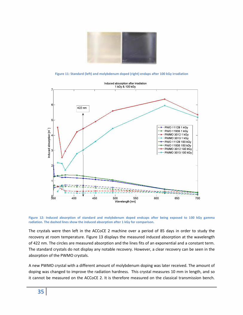
of the spectrum. Figure 11 shows the front face of the crystals as viewed with the naked eye. The left
crystal is a standard PWO crystal and the right one a PWMO crystal.
35
Figure 11: Standard (left) and molybdenum doped (right) endaps after 100 kGy irradiation
Figure 12: Induced absorption of standard and molybdenum doped endcaps after being exposed to 100 kGy gamma radiation. The dashed lines show the induced absorption after 1 kGy for comparison.
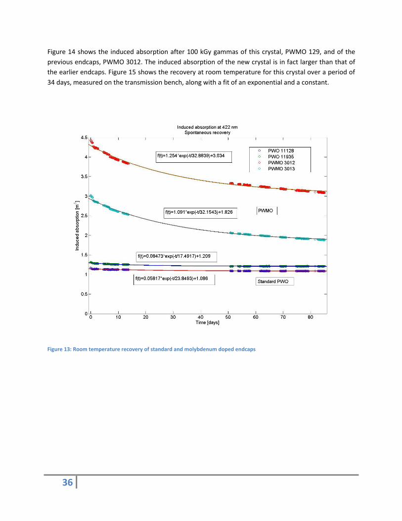
The crystals were then left in the ACCoCE 2 machine over a period of 85 days in order to study the
recovery at room temperature. Figure 13 displays the measured induced absorption at the wavelength
of 422 nm. The circles are measured absorption and the lines fits of an exponential and a constant term.
The standard crystals do not display any notable recovery. However, a clear recovery can be seen in the
absorption of the PWMO crystals.
A new PWMO crystal with a different amount of molybdenum doping was later received. The amount of
doping was changed to improve the radiation hardness. This crystal measures 10 mm in length, and so
it cannot be measured on the ACCoCE 2. It is therefore measured on the classical transmission bench.
36
Figure 14 shows the induced absorption after 100 kGy gammas of this crystal, PWMO 129, and of the
previous endcaps, PWMO 3012. The induced absorption of the new crystal is in fact larger than that of
the earlier endcaps. Figure 15 shows the recovery at room temperature for this crystal over a period of
34 days, measured on the transmission bench, along with a fit of an exponential and a constant.
Figure 13: Room temperature recovery of standard and molybdenum doped endcaps

37
Figure 14: Induced absorption of PWMO 129. The blue curve shows the induced absorption of PWMO 129 at 100 kGy. The green curve shows the induced absorption of crystal PWMO 3012 at the same dose, for comparison.

38
Figure 15: Room temperature recovery of PWMO 129
4.1.2 Thermal bleaching
After several days at room temperature, the absorption spectrum recovers very slowly or not at all. To
accelerate the recuperation process, the crystals are heated. In effect, the colour centres of the crystals
are destroyed by thermal activation. The oven used is a Nabertherm TR 60, equipped with a Nabertherm
S 27 controller unit. The maximum temperature of the oven is 300ºC, and so this is the highest
temperature at which we can study recovery. When the crystals are placed in the oven, the
temperature is raised to the point that is being studied. The temperature is maintained for a predefined
amount of time, after which the oven is allowed to cool. The crystals are taken out and measured on the
transmission bench. Figure 16 shows evolution of the induced absorption at 420 nm for a standard
endcap crystal and a molybdenum doped crystal. The time taken to bring the temperature to the
specified point or cool the oven is not included in the time specified on the x-axis. There is limited
recovery at 50 ºC, but a distinct recovery can be seen for temperatures of 100ºC and higher. At 200ºC
there is complete recovery.

39
Figure 16: Thermal bleaching of standard and molybdenum doped endcaps.
4.1.3 Optical bleaching
An alternative possible way of recovery is to destroy the colour centre by illumination with light of a well chosen wavelength. A trapped electron is a system analogous to a hydrogen atom. It has different energy levels and can thus be excited by a ray of light. If the trapped electron acquires a high enough energy it can escape the trap, migrate in the crystal and recombine with a hole. To test this, prototype box with nine LEDs was produced, as seen in Figure 17. Two different sets of LEDs have been used. The first set is a set of diodes of the type B56L5111P from Roithner Lasertechnik, emitting at a wavelength of 475 nm. The second set uses diodes of the type ELD-740-524, also from Roithner Lasertechnik, emitting at a wavelength of 740 nm. The crystals are placed in front of the diodes so that the front face is illuminated. They are covered with black cloth to isolate them from other light sources. Figure 18 shows the induced absorption at 420 nm of a standard endcap crystal as well as a molybdenum doped crystal after treatment with optical bleaching. Some recovery can be observed at 475 nm, but none at 740 nm. In comparison to the thermal bleaching the effect is very small. The short molybdenum doped crystal was also treated with optical bleaching. The induced absorption at 420 nm for this crystal is displayed in Figure 19. There is little effect with the 475 nm diodes, but a notable effect with the 740 nm diodes.

40
Figure 17: Optical bleaching setup
Figure 18: Optical bleaching of standard and molybdenum doped endcaps

41
Figure 19: Optical bleaching of PWMO 129
4.2 Proton irradiation The effects of proton irradiation were studied on a number of PWO crystals measuring 10*10*20 mm2
cut from a standard endcap crystal. They were first irradiated with gamma rays to compare the
absorption spectra with those of the standard endcap crystals. Figure 20 and Figure 21 show the
induced absorption of standard endcap crystals compared to the small crystals for 1 kGy and 100 kGy
gammas respectively. Due to the shorter length of the small crystals, the measurements are more
sensitive to fluctuations than those of the endcap crystals. However, the general shapes of the spectra
are the same for endcap and small crystals. The small crystals were then irradiated with protons. Table 2
summarises the fluences and the rates the different crystals were exposed to. The induced absorption at
420 nm for the different crystal samples and the evolution at room temperature are displayed in Figure
22.

42
Sample Gammas Protons
1.1 1kGy 1.39E+13 p/cm
2
, 1.16E+13 p/cm2
h
1.2 1kGy 1.51E+13 p/cm
2
, 1.33E+12 p/cm2
h
2.4 1kGy 1.39E+13 p/cm
2
, 1.16E+13 p/cm2
h
3.1 100kGy 1.51E+13 p/cm
2
, 1.33E+12 p/cm2
h
3.3 1.64E+14 p/cm
2
, 1.3E+14 p/cm2
h
5.1 4.53E+13 p/cm
2
, 5.5E+13 p/cm2
h
5.2 2.26E+14 p/cm
2
, 4.6E+13 p/cm2
h
5.3 2.26E+14 p/cm
2
, 4.6E+13 p/cm2
h 5.4
8E+14 p/cm2
, 5.6E+13 p/cm2
h Table 3: Irradiation of small PWO samples. The centre column shows the gamma irradiation dose if performed. The rightmost column shows the flux and fluence of the proton irradiation.
Figure 20: Comparison of induced absorption after 1 kGy gamma irradiation of standard endcaps and small samples

43
Figure 21: Comparison of induced absorption after 100 kGy gamma radiation of standard endcap and small sample
44
Figure 22: Room temperature recovery of small samples of lead tungstate
4.2.1 Thermal Bleaching
Three of the small crystal samples were treated with thermal bleaching: 3.3, 5.2 and 5.4. However, the
samples 5.2 and 5.4 were damaged and so only sample 3.3 has been studied over a full range of
temperatures. Figure 23 shows the recovery of induced absorption at 420 nm for all three crystals with
thermal annealing. There is little recovery at 50 ºC, followed by a notable recovery at 100 ºC. Figure 24
shows the recovery of sample 3.3 over the full range of temperatures. After several hundreds of hours
at 300 ºC, all damage at 420 nm is recovered.

45
Figure 23: Thermal bleaching of proton irradiated samples

46
Figure 24: Thermal bleaching of proton irradiated sample 3.3
4.2.3 Optical Bleaching
One small sample, 5.3, has been treated with optical bleaching. The recovery at 420 nm is displayed in
Figure 25. There is a notable recovery in the first 35 hours after which the absorption levels off. There is
also some recovery when using the 740 nm diodes.

47
Figure 25: Optical bleaching of proton irradiated sample 5.3
4.3 Diffusion An effect that has been observed in proton irradiated crystal is the diffusion of light. To study this, a
diffusion bench has been constructed. The bench consists of a laser, a beam splitter, a photodiode, a
crystal holder and a camera. The beam splitter splits the beam from the laser in two beams, one that
goes to a photodiode to measure the power of the laser and one that goes into the crystal. The camera
is fixed in place above the crystal. In an ideal case, the beam going through the crystal should not be
diffused at all and so nothing should be visible from the sides of the crystal. By taking a picture with the
camera from above, the amount of diffusion can be measured. Figure 26 shows the pictures taken of
series 5 before and after irradiation. From top to bottom they are sample 5.1, 5.2, 5.3 and 5.4. From left
to right the pictures are before irradiation, top face after irradiation and side face after irradiation.
There is a clear polarisation in the sample. This cannot be accurately quantified however, because the
difference in light between the sides before irradiation was not measured. Figure 27 shows the
difference in collected light from the top face for the different samples. The most irradiated samples are
the ones displaying the largest amount of diffusion. Figure 28 shows the light collected from the top face
of crystal 3.3 after finishing one temperature with thermal annealing, along with the amount of light
collected. After treatment at 100 ºC, there is a clear decrease in diffusion. The remaining diffusion likely
pertains to mechanical surface damage rather than crystal defects.

48
Figure 26: Induced diffusion in proton irradiated samples. From top to bottom: Samples 5.1, 5.2, 5.3 and 5.4. From left to right: Before irradiation, top face after irradiation, side face after irradiation.
Figure 27: Difference in collected light before and after irradiation for samples 5.1,5.2,5.3 and 5.4
0
5
10
15
20
25
5.1 5.2 5.3 5.4

49
Figure 28: Recovery of diffusion with thermal bleaching in sample 3.3
4.4 Proton irradiation of standard endcaps Twelve standard Endcap crystals were irradiated by protons at the PS facility IRRAD 3 at CERN. Ten of
the crystals were produced at BTCP in Russia and two at SIC in China. The crystals were irradiated at a
rate of 2*1012 p/cm2h, for a total fluence of 2*1013 p/cm2. Because of the high induced activation of the
crystals, it is important to avoid manual manipulation of the crystals. For this reason, a special setup was
constructed by the technicians of PH-CMX. A dedicated spectrophotometer was supplied by the MINSK
group to allow for transmission measurements of the crystals without removing them from the room.
The setup can be seen in Figure 29.
Figure 29: Irradiation setup
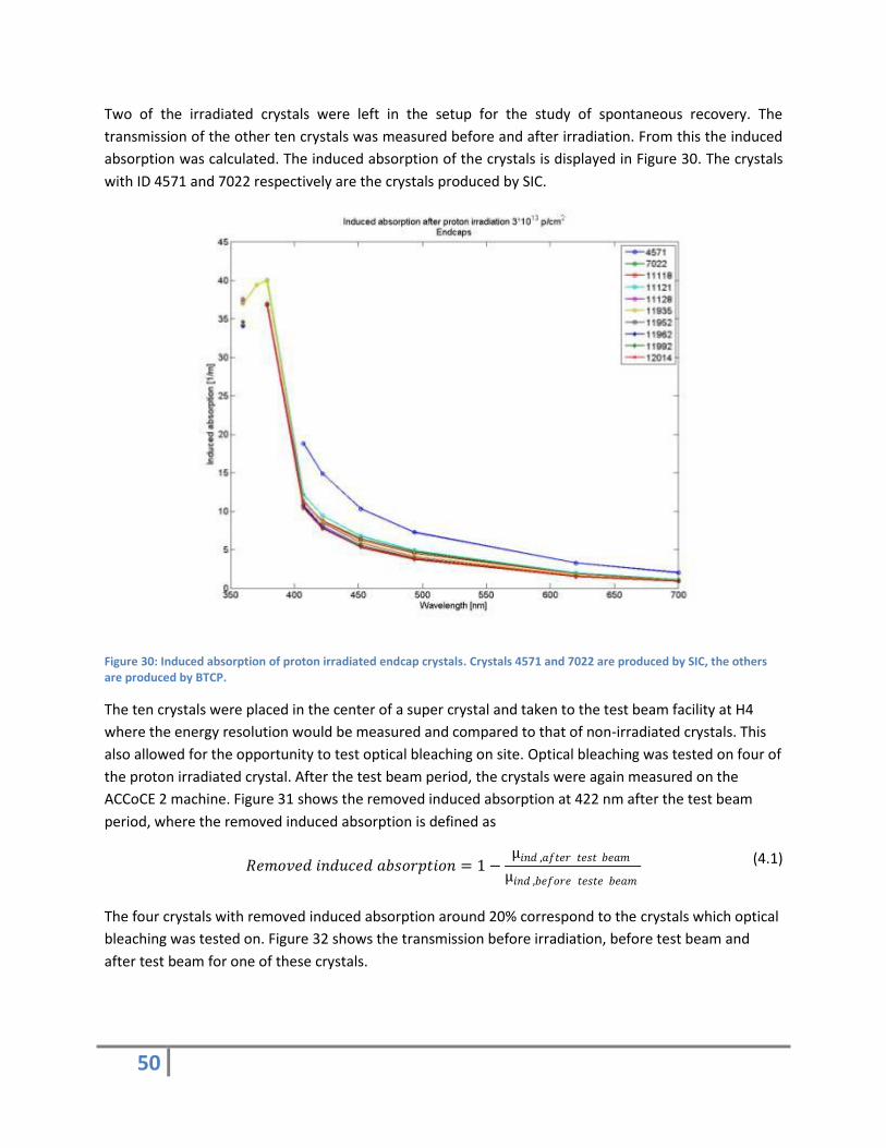
50
Two of the irradiated crystals were left in the setup for the study of spontaneous recovery. The
transmission of the other ten crystals was measured before and after irradiation. From this the induced
absorption was calculated. The induced absorption of the crystals is displayed in Figure 30. The crystals
with ID 4571 and 7022 respectively are the crystals produced by SIC.
Figure 30: Induced absorption of proton irradiated endcap crystals. Crystals 4571 and 7022 are produced by SIC, the others are produced by BTCP.
The ten crystals were placed in the center of a super crystal and taken to the test beam facility at H4
where the energy resolution would be measured and compared to that of non-irradiated crystals. This
also allowed for the opportunity to test optical bleaching on site. Optical bleaching was tested on four of
the proton irradiated crystal. After the test beam period, the crystals were again measured on the
ACCoCE 2 machine. Figure 31 shows the removed induced absorption at 422 nm after the test beam
period, where the removed induced absorption is defined as
𝑅𝑒𝑚𝑜𝑣𝑒𝑑 𝑖𝑛𝑑𝑢𝑐𝑒𝑑 𝑎𝑏𝑠𝑜𝑟𝑝𝑡𝑖𝑜𝑛 = 1 −µ𝑖𝑛𝑑 ,𝑎𝑓𝑡𝑒𝑟 𝑡𝑒𝑠𝑡 𝑏𝑒𝑎𝑚
µ𝑖𝑛𝑑 ,𝑏𝑒𝑓𝑜𝑟𝑒 𝑡𝑒𝑠𝑡𝑒 𝑏𝑒𝑎𝑚
(4.1)
The four crystals with removed induced absorption around 20% correspond to the crystals which optical
bleaching was tested on. Figure 32 shows the transmission before irradiation, before test beam and
after test beam for one of these crystals.

51
Figure 31: Removed induced absorption after test beam period at 422 nm.
Figure 32: Transmission of crystal 11128 before irradiation, after irradiation and after bleaching in test beam.
-5
0
5
10
15
20
25
0 2 4 6 8 10 12
Re
mo
ved
ab
sorp
tio
n [
%]
Crystal
Removed induced absorption at 422 nm
4571
7022
11118
11121
11128
11935
11952
11962
11992
12014
0
0,1
0,2
0,3
0,4
0,5
0,6
0,7
0,8
0,9
340 440 540 640
Tran
smis
sio
n
Wavelength[nm]
11128
Initial transmission
Irradiated
Bleached

52
Chapter 5
Comparison of Light Yield for Different Sources Scintillating materials may react differently to different type of sources. Protons, α-particles and heavy
ions are weakly penetrating particles. Because the light output of a scintillator not only depends on the
energy losses of the incident particle but also on the density of ionization, the light output decreases.
The consequence is that for equal energies, protons and α-particles produce less light than electrons.
Neutrons are uncharged particles and do not ionize the material. The neutrons instead transfer energy
to the atomic nuclei by means of the strong force. The scintillation is produced when the excited nuclei
transfer to the ground state. The difference in light yield of different crystals depending on the type of
incident particles has been investigated. The different sources are gamma, alpha and neutron sources.
The crystals studied are LYSO, LuYAP, BGO, NaI, CsI, LaBr3 and PWO.
5.1 Light Yield Measurements In a light yield measurement, a radioactive source is used to initiate the scintillation process in the
crystal that is being studied. The light produced by the crystal is detected by a photomultiplier tube. The
sources that have been compared are two gamma sources, 60Co and 137Cs, an alpha source, 241Am, and a
neutron source, AmBe. The crystal being measured is placed on the window of the photomultiplier tube
with optical grease (n≈1.5) between the two surfaces. The purpose of the grease is to reduce the
amount of light reflected at the interface between the media. The crystal sides are wrapped with
reflective Teflon to prevent the loss of scintillation light through the sides of the crystal. As the light yield
may vary with temperature a cooling unit is installed to maintain a constant temperature, typically 18ºC.
Photons detected by a photomultiplier tube are absorbed by the photocathode. Through the
photoelectric effect, the energy of the photons is transferred to an electric flux. The electron flux is
multiplied through a series of dynodes before being collected by the anode and converted to an output
signal. The efficiency with which the energy of the photons are converted to electrons is known as the
Quantum Efficiency and is defined as follows:
𝑄𝐸 =𝑁𝑢𝑚𝑏𝑒𝑟 𝑜𝑓 𝑒𝑚𝑖𝑡𝑡𝑒𝑑 𝑝𝑜𝑡𝑜𝑒𝑙𝑒𝑐𝑡𝑟𝑜𝑛𝑠
𝑁𝑢𝑚𝑏𝑒𝑟 𝑜𝑓 𝑖𝑛𝑐𝑖𝑑𝑒𝑛𝑡 𝑝𝑜𝑡𝑜𝑛𝑠
(5.1)
This quantity generally varies with wavelength. Figure 33 shows a sketch of a photomultiplier tube.

53
Figure 33: Principle of a photomultiplier tube
5.1.1 Classical Light Yield Bench 4
The light yield measurements have been conducted on bench 4. The light produced by the crystal being
measured is detected by a Photonis XP2262B photomultiplier tube. The photomultiplier tube is placed
in a box which is covered by black cloth when a measurement is running to avoid any external light
influencing the measurement. The bench is equipped with a Lauda RC 6 CS cooling system to maintain a
stable temperature. The signal from the photomultiplier tube is collected by a LeCroy waveRunner 104Xi
oscilloscope. Figure 34 shows a sketch of the electronics connecting the bench to the oscilloscope.
Figure 34: Setup of bench 4
HV 2200 Volt
Oscilloscope
Attenuators
PMT
Source
Crystal
Sealed box

54
When a signal from the photomultiplier tube is detected a gate signal is generated. The signal from the
photomultiplier tube is then integrated during the time the gate signal is high.
Figure 35: Scintillation pulse of LYSO
The part from 0 to 1 ns of the signal is also integrated and multiplied by five. This integral represents
the electronic noise and provides the level of zero energy. Subtracting this value from the first integral
gives the energy of the photoelectrons from the PMT. The values of the integral are stored and added to
a histogram which results in a spectrum displaying the characteristics of the scintillation.
5.1.2 Extraction of Light Yield
To properly determine the light yield of a crystal, two measurements are performed. First, a
measurement without any crystal or source is used. In this case the normal conduction electrons within
the photocathode, which occasionally have enough energy to escape the photocathode, are detected.
This results in a spectrum with a single peak representing the energy of a single electron. The second
measurement is done with the crystal being studied and a radioactive source. This produces a spectrum
representing the scintillation events in the studied crystal. Figure 36 shows a spectrum obtained from an
LYSO crystal using a 137Cs source.
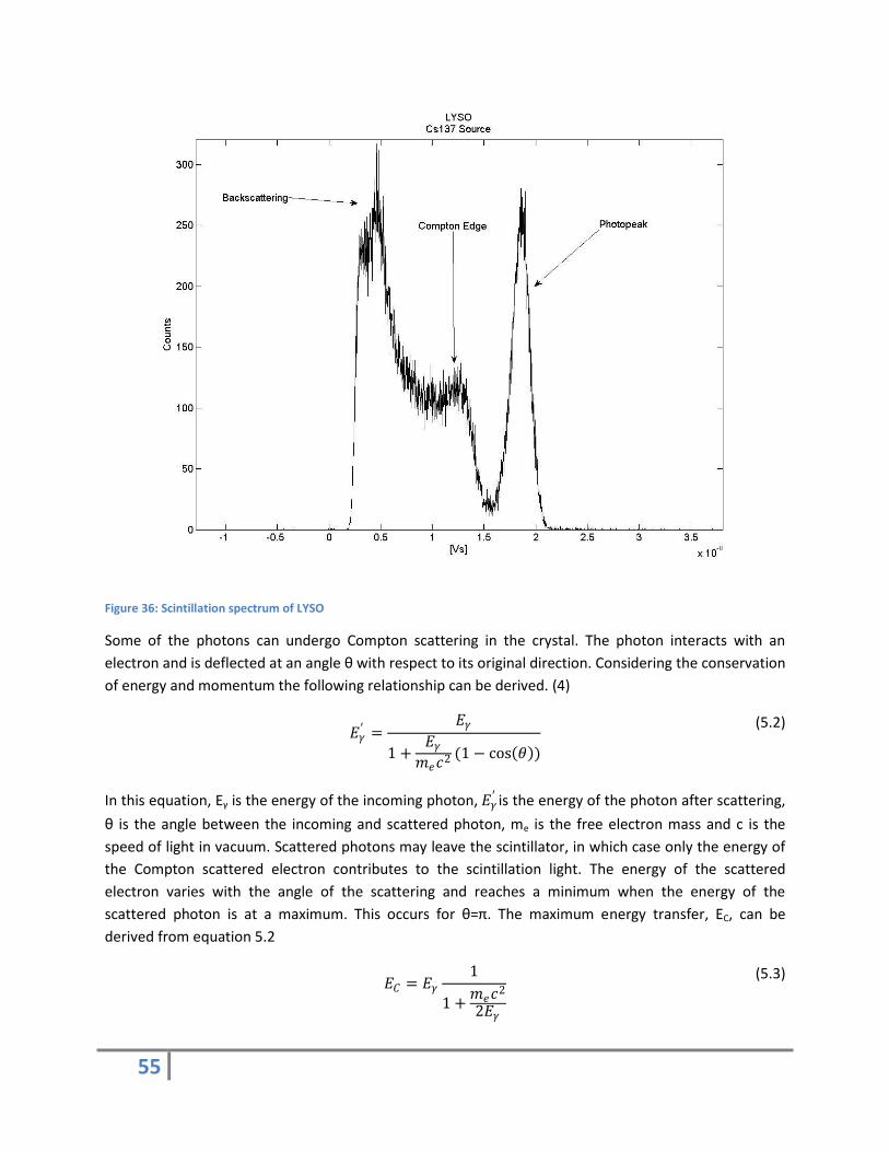
55
Figure 36: Scintillation spectrum of LYSO
Some of the photons can undergo Compton scattering in the crystal. The photon interacts with an
electron and is deflected at an angle θ with respect to its original direction. Considering the conservation
of energy and momentum the following relationship can be derived. (4)
𝐸𝛾
′ =𝐸𝛾
1 +𝐸𝛾
𝑚𝑒𝑐2 (1 − cos 𝜃 )
(5.2)
In this equation, Eγ is the energy of the incoming photon, 𝐸𝛾′ is the energy of the photon after scattering,
θ is the angle between the incoming and scattered photon, me is the free electron mass and c is the
speed of light in vacuum. Scattered photons may leave the scintillator, in which case only the energy of
the Compton scattered electron contributes to the scintillation light. The energy of the scattered
electron varies with the angle of the scattering and reaches a minimum when the energy of the
scattered photon is at a maximum. This occurs for θ=π. The maximum energy transfer, EC, can be
derived from equation 5.2
𝐸𝐶 = 𝐸𝛾
1
1 +𝑚𝑒𝑐
2
2𝐸𝛾
(5.3)

56
This is the absolute maximum of energy that a photon may transfer to an electron. This limit results in a
sharp edge in the scintillation spectrum called the Compton edge. This is visible in Figure 36. The
Backscattering peak, also visible in Figure 36, is caused by gamma rays scattered in the surrounding
environment, such as the source shielding and crystal holder. The photopeak is the far right peak in the
spectrum of Figure 36. This is the peak which characterizes the light yield of the scintillator. By fitting a
Gaussian to the photopeak the position of the photopeak may be determined. The number of
photoelectrons is found by dividing the position of the photopeak by the position of the single electron
peak. The number of photoelectrons per MeV of energy is found according to the following equation.
𝑁𝑝𝑒
𝑀𝑒𝑉=
𝑃𝑜𝑠𝑖𝑡𝑖𝑜𝑛 𝑜𝑓 𝑝𝑜𝑡𝑜𝑝𝑒𝑎𝑘
𝑃𝑜𝑠𝑖𝑡𝑖𝑜𝑛 𝑜𝑓 𝑠𝑖𝑛𝑔𝑙𝑒 𝑒𝑙𝑒𝑐𝑡𝑟𝑜𝑛 𝑝𝑒𝑎𝑘∗
10𝐴
20
𝐸𝑠
(5.4)
In this expression, A is the value of any applied attenuation in dB and Es is the energy of the particles
emitted by the radioactive source. To find the true light yield, this number needs to be divided by the
quantum efficiency of the PMT. In this exercise, where we are comparing the light yield of a crystal for
different sources, the quantum efficiency will be the same for all sources and it is sufficient to compare
the number of photoelectrons.
5.1.3 Light Yield for Different Sources
Table 3 shows the particles emitted by the utilized sources. The energies and the relative intensities of
the particles are included.
Co60 (9) Cs137 (9) Am241 (9) AmBe (10)
Gamma (E [keV,%)
1332.5, 99.99% 1173.2, 99.97%
661.657, 85.1 % 59.5412, 35.9 %
Alpha (E [keV],%)
5485.56 , 84.5 % 5442.80 ,13.0 %
Beta (E [keV,%)
318.13 , 99.93 % 513.97 , 94.4 %
Neutron (E [keV])
~3000 ~5000 ~8000
Table 4: Radioactive sources utilized for light yield measurements
Co60 and Cs137 are both gamma sources, and measurements done with these sources should thus
result in the same light yield. The Co60 source displays two different energy peaks, and the spectrum
acquired with this source should thus show two distinct photopeaks, as seen in Figure 37. However, in
the case of low light yield crystals it may not be possible to accurately distinguish the two peaks. If this is
the case, the mean energy of the gammas is used. The neutron source AmBe presents a similar case. For
crystals with high light yield, three peaks can be observed. Figure 38 is an example of this. If only one
peak is observed, the energy of the source is taken as 5 MeV.

57
Figure 37: Light yield spectrum of a LYSO crystal using a Co60 source
Figure 38: Light yield spectrum of an NaI crystal using an AmBe source

58
Table 4 summarizes the light yield obtained with the different sources. In the second far right column
the quota of the light yields obtained with the Am241 and Cs137 sources is displayed and in the second
far right column the quota of the light yield from the AmBe and Cs137 sources.
Co60 [γ] Cs137 [γ] Am241 [α] AmBe [Neutron]
α/γ Neutron/γ
LYSO 4150.668963 4555.593012 259.9321932 250.2387929 0.057057817 0.054930015
4104.700314
LUYAP 1589.680324 1699.296101 87.96807366 92.89167313 0.05176736 0.054664795
1707.498005
BGO 715.3370343 762.4879575 116.3136346 89.68348348 0.152544881 0.117619541
NaI 10499.14618 15157.56395 1441.030962 8570.046899 0.09507009 0.565397377
17543.49889
5835.471997
0.384987457
4019.744001
0.265197232
CsI 8321.975833 8907.815911 56.06610024 5443.662078 0.006294034 0.611110752
12298.87846
3790.323953
0.42550542
2685.075341
0.301429146
CsIpure No Peak 83.71887429 22.42017758 58.74514159 0.267803142 0.701695312
LaBr3 7576.376038 11646.98719 1560.928573 4046.335176 0.134019944 0.347414753
7356.52227
2544.753245
0.218490259
1647.902632
0.14148746
Table 5: Summary of light yield measurements
It can be seen that the calculated light yield for the AmBe source, in the case where there are three
distinct peaks, differs for the three peaks. It is possible that the interpretation of the spectrum is wrong.
The calculation of the number of photoelectrons produced versus the energy of the source for these
cases is plotted in Figure 39. The equations of trendlines are summarized in Table 6.

59
Figure 39: Number of photoelectrons versus energy for NaI, CsI and LaBr3 using an AmBe source
Crystal Slope Constant
NaI 1266.2 PE/MeV 22262 PE
CsI 1015.2 PE/MeV 13507 PE
LaBr3 204.45 PE/MeV 11592 PE Table 6: Trendlines for NaI, CsI and LaBr3 using an AmBe source
0
5000
10000
15000
20000
25000
30000
35000
0 2 4 6 8 10
Nu
mb
er
of
ph
oto
ele
ctro
ns
Energy [MeV]
Number of photelectrons vs energy
NaI
CsI
LaBr3

60
Chapter 6
Discussion and Conclusions
6.1 Irradiation damage and recovery
6.1.1. Gamma Irradiation
At a dose of 1 kGy, irradiated with gammas, the induced absorption for the standard PWO crystals PWO
11128 and PWO 11935 is 0.7032 m-1 and 0.6007 m-1 respectively at 422 nm. For the same dose and
wavelength the induced absorption of the molybdenum doped crystals PWMO 3012, PWMO 3013 and
PWMO 3014 is 0.3182 m-1, 0.2013 m-1 and 0.2216 m-1 respectively. See Figure 10. When increasing the
dose to 100 kGy the induced absorption for crystals PWO 11128 and 11935 at 422 nm is found to be
1.167 m-1 and 1.32 m-1 respectively. At the same wavelength and dose the induced absorption of the
molybdenum doped crystals PWMO 3012 and PWMO 3013 is 4.432 m-1 and 3.026 m-1 respectively. See
figure Figure 12. Molybdenum doped crystals thus seem to be more resistant to radiation damage at low
dose rates, but perform worse at high doses. It can also be noted that the peak in the induced
absorption is shifted towards higher wavelengths for the molybdenum doped crystals. For standard
crystals a peak can be discerned in the vicinity of 400 nm. For molybdenum doped crystals, the
maximum value is found in the vicinity of 600 nm. It is possible that the doping does in fact suppress the
formation of the defects found in standard PWO crystals, but at high doses introduces a new kind of
defect with an absorption centred on 600 nm. Leaving the crystals in room temperature and monitoring
the induced absorption over time shows that the induced absorption at 422 nm of standard crystals
remain at the same level. This can be seen in Figure 13. The induced absorption of the molybdenum
doped crystals show an initial recovery, but remains larger than that seen in the standard crystals.
Fitting the sum of an exponential and a constant gives a time constant of 32.9 days for PWMO 3012 and
32.2 days for PWMO 3013.
Crystals PWO 11128 and PWMO 3012 were treated with thermal bleaching. The results of the treatment
are very similar for the two crystals. Figure 16, shows the induced absorption at 420 nm plotted versus
the time spent in thermal bleaching for the two crystals. At 50ºC there is a minor recovery, and when
the temperature is increased to 100ºC a strong recovery process can be observed. Fitting a sum of an
exponential and a constant to this segment of the curve yields a time constant of 4.6751 hours for PWO
11128 and 4.0437 hours for PWMO 3012. When further increasing the temperature to 150 ºC the
process is accelerated and after treatment at 200 ºC there is no remaining induced absorption.
Crystals PWO 11935 and PWMO 3013 where treated by means of optical bleaching, first with light of
wavelength 475 nm and then with light of wavelength 740 nm. The induced absorption at 420 nm of
these two crystals is shown in Figure 18. A slight recovery can be seen when using 475 nm light,
particularly for crystal PWO 11935. At 740 nm there is little to no effect. Crystal sample PWMO 129 was
also treated with optical bleaching, and the results can be seen in Figure 19. For this crystals there is
little to no effect at 475 nm, but a clear recovery at 740 nm. Considering that the spectra of induced

61
absorption, shown in Figure 12 and Figure 14, showed a peak near 400 nm for standard crystals and a
peak near 600 nm for the molybdenum doped crystals, it is likely that wavelengths closer to the peak of
the absorption spectrum are more effective.
6.1.2 Proton Irradiation
A number of small samples cut from a standard endcap crystal were irradiated with various doses of
protons. Of these, one sample has been treated with optical bleaching and three with thermal
bleaching. Unfortunately, two of the samples treated with thermal bleaching where damaged during the
treatment and so only partial data are available for these samples. Figure 23 show the induced
absorption at 420 nm versus time spent in thermal bleaching of all three samples treated thermally.
There is little to no recovery at 50 ºC, followed by a slight but noticeable recovery at 100 ºC. The
complete recovery cycle for the undamaged sample, sample 3.3, can be seen in Figure 24. Complete
recovery is achieved, but not until after several hundred of hours at 300 ºC.
Sample 5.3 was treated with optical bleaching and the results are shown in Figure 25. There is a clear
recovery when using the 475 nm light, but it quickly reaches a plateau. When switching to the 740 nm
light, there is some further limited recovery.
As seen in Figure 26, the proton irradiated samples display a clear diffusion. A polarization effect can be
observed, however it cannot be accurately quantified because prior to the irradiation pictures were only
taken of one side. A notable reduction in diffusion is observed when using thermal bleaching at 100 ºC.
So far no reduction in diffusion using optical bleaching has been demonstrated. That the diffusion can be
recovered using thermal bleaching suggests it is also caused by absorption centres, and not a more
profound structural damage.
Ten standard encap crystals were irradiated with protons and measured in the test beam. Four of these
were treated with optical bleaching during the test beam. The treated crystals display a reduction in
induced absorption by 20%. The induced absorption of the non-treated crystals remains at the same
levels.
6.2 Comparison of light yield for different sources The light yield of crystal samples of LYSO, LUYAP, BGO, pure CsI, doped CsI and LaBr3 was measured
using different sources. The sources used were Cs137, Co60, Am241 and AmBe. Cs137 and Co60 are
gamma sources, Am241 is an alpha source and AmBe is a neutron source. The measurements show that
all measured crystals consistently produce less light when subjected to alpha radiation and neutrons
than when subjected to gamma radiation. The fraction of light yields achieved with alpha radiation
compared to gamma radiation ranges from 5% (LUYAP) to 27% (Undoped CsI). The fraction of light yields
achieved with neutrons compared to gamma radiation ranges from 5% (LUYAP) to 70% (Undoped CsI).
NaI, doped CsI and LaBr3 display three distinct peaks when measured with the neutron source (AmBe).
It is known that AmBe possesses three emission peaks, and so it would be natural to assume that each
emission peak is the source of one corresponding peak in the light yield spectrum. When using the
energies of the emission peaks to calculate the light yield, however, each peak produces a different
result, with the lowest energy peak giving the highest light yield. This work can produce no explanation

62
for why this is the case. One possibility is that the two extra peaks do not originate from the different
emission peaks, but could perhaps be some form of backscattering or Compton edge.
6.3 Future work In this work, recovery of proton irradiation damage has been limited to 10*10*20 mm3 samples. It has
been shown that thermal bleaching can fully recover the transmission of proton irradiated crystal.
Optical bleaching has been shown to have an effect, but so far only a limited effect. In order to complete
the study, tests must be performed on full size endcap crystals. Ten endcap crystals have been
irradiated, and limited tests with optical bleaching have been performed in test beam. Complete tests
with both thermal and optical bleaching should be performed for the proton irradiated endcap crystals
just as they were for the gamma irradiated endcaps in this work.
The tests of optical bleaching in this work have been limited to two wavelengths, 475 and 740 nm. Using
different wavelengths may yield a stronger recovery, and so it is interesting to test as many wavelengths
as feasible. LEDs with emission peaks at 360 nm, 590 nm and 625 nm have been purchased.
In order to better understand the nature of the defects in the PWO crystals it is of interest to study the
thermoluminescence of the crystals. This will require the construction of a dedicated
thermoluminescence bench. This bench must be able to control the temperature and simultaneously
measure light output and temperature. For this purpose a PID controller and thyristor unit has been
purchased from Eurotherm.

63
Bibliography 1. CMS - Detector. CMS Experiment. [Online] [Cited: December 18, 2010.]
http://cms.web.cern.ch/cms/Detector/Work/index.html.
2. Collaboration, CMS. The Electromagnetic Calorimeter Technical Design Report. 1997. CERN/LHCC 97-
33.
3. Roldan, Pablo Sempere. Quality control and preparation of the PWO crystals for the electromagnetic
calorimeter of CMS. s.l. : University of Santiago de Compostela, 2001.
4. Rodnyi, Piotr A. Physical Processes in Inorganic Scintillators, book, CRC-Press, 1997.
5. Nedfors, Nils. Karakterisering av bly-wolfram-oxid kristallers, Master Thesis, Linköping University,
2008.
6. LeCoq, Paul. Inorganic Scintillators for Detector System, book, Springer, 2006.
7. Auffray, Etiennette. Etude des mécanismes de scintillation et des modifications sous irradiation des
propriétés du fluorure de cérium en vue de son utilisation en calorimétrie électromagnétique de haute
résolution, Doctoral Thesis, University of Paris, 1995.
8. Rostaing, Bruno. Etude de la thermoluminescence et des dommages par irradiations dans des
monocristaux de germanate de bismuth (Bi4Ge3O12), Doctoral Thesis, Grenoble Institute of Technology,
1988
9. S.Y.F. Chu, L.P. Ekström and R.B. Firestone. The Lund/LBNL Nuclear Data Search. [Online] [Cited: 11
06, 2010.] http://nucleardata.nuclear.lu.se/nucleardata/toi/.
10. Neutron energy spectra of 252Cf, Am–Be source and of the D(d,n)3He reaction. Park, Sang-Tae.
2002, Vols. Journal of Radioanalytical and Nuclear Chemistry, vol 256.
11. Presentation at SLHC Electronics Workshop. Huhtinen, M. 2004.