Embed Size (px)
Citation preview

Structured Hardware Design
Six lectures for CST Part Ia (50 percent).
Easter Term 2005.
(C) DJ Greaves.
1

Preface
There are a few more slides here than will be
used in lectures. No Verilog is examinable: it is
provided for reference use in part Ib. The first
ten or so slides are revision of material from
digital electronics.
At least 10 minutes or so of each lecture will
be devoted to example material, including pre-
vious exam questions, for which there are no
slides in this handout.
2

Books related to the course
Suggested books include:
Bignell & Donovan. ‘Digital Electronics’ Del-
mar Publishers.
W.Ditch. ‘Microelectronic Systems, A practi-
cal approach.’ Edward Arnold. The final chap-
ters with details of the Z80 and 6502 are not
relevant to this course.
Floyd. ‘Digital Fundamentals’ Prentice Hall
International.
T.J. Stoneham. ‘Digital Logic Techniques’
Chapman and Hall. This is a basic book and
relates more to the previous course on Digital
Electronics.
Randy H Katz. ‘Contemporary logic design.’
3

Encoder and Decoder(Revision)
Priority Encoder
Q2
d0d1d2d3
Q0Q1d0 d1 d2 d3
1 1
1 0
0 1
0 0
x x x 1
x x 1 0
x 1 0 0
x 0 0 0
module priencoder(d, Q);output [1:0] Q;input [3:0] d;assign Q = d[3] ? 2’d3: d[2] ? 2’d2: d[1] ? 2’d1: 2’d0;
endmodule
Binary to Unary Decoder
Q2
d0d1d2d3
Q0Q1 d0 d1 d2 d3
1 1
1 0
0 1
0 0
1
1 0
1 0 0
0 0 01
0 0 0
0 0
0
module decoder(Q, d);input [1:0] Q;output [3:0] d;assign d0 = (Q==2’d0); assign d1 = (Q==2’d1);assign d2 = (Q==2’d2); assign d3 = (Q==2’d3);
endmodule
4
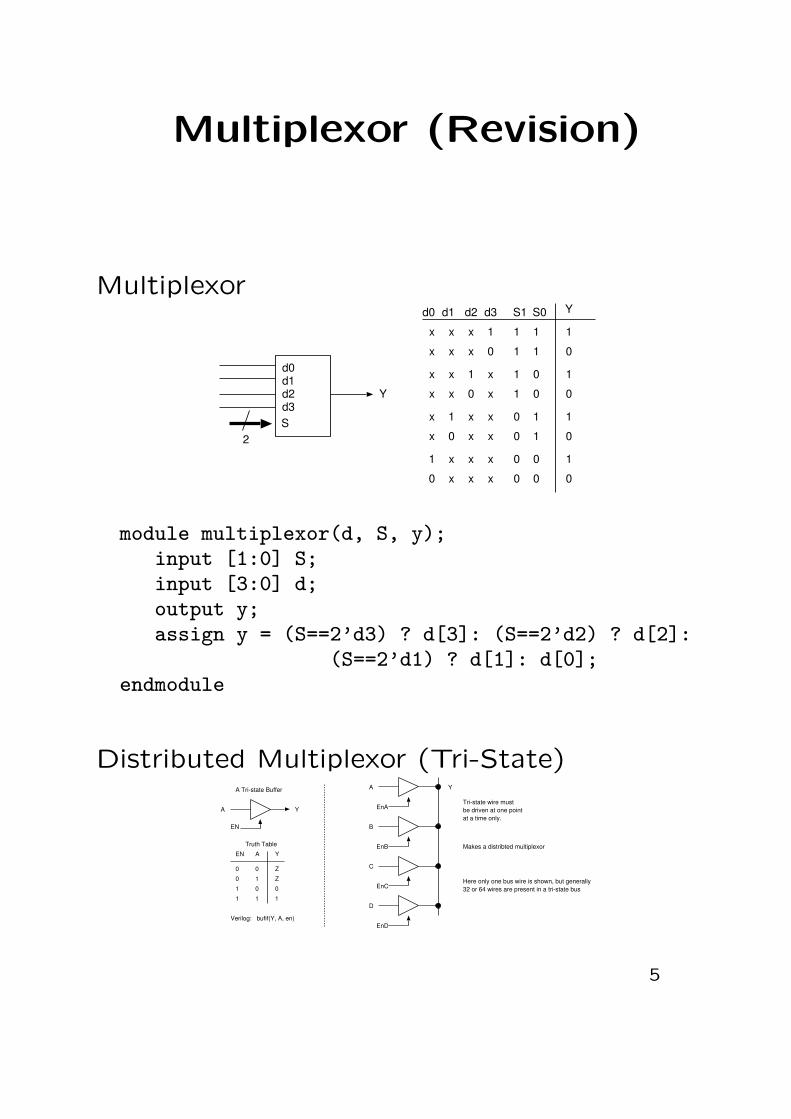
Multiplexor (Revision)
Multiplexor
Y
d0d1d2d3
S0S1d0 d1 d2 d3
1 1x x x 1
S2
x x x 0 1 1
1
0
Y
1xx x 1
xx x 0 1
1
0
1x xx1
x xx0 1
1
0
xx x1
xx x0
1
0
0
0
0
0
0
0
0
0
module multiplexor(d, S, y);input [1:0] S;input [3:0] d;output y;assign y = (S==2’d3) ? d[3]: (S==2’d2) ? d[2]:
(S==2’d1) ? d[1]: d[0];endmodule
Distributed Multiplexor (Tri-State)
A Y
EN
AEN Y
0
1
Z
1
0
0
1 1
0
Z
1
0
A Tri-state Buffer A
EnA
B
EnB
C
EnC
D
EnD
Tri-state wire mustbe driven at one pointat a time only.
Makes a distribted multiplexor
Here only one bus wire is shown, but generally32 or 64 wires are present in a tri-state bus
Truth Table
Verilog: bufif(Y, A, en)
Y
5

Barrel Shifter
3
d0d1d2d3d4d5d6d7
q0q1q2q3q4q5q6q7
sh
6
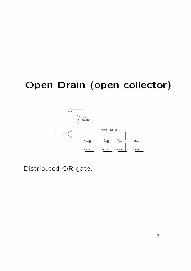
Open Drain (open collector)
+5 Volt
Y
Ground Ground Ground Ground
Pull UpResistor
a1 a2 a3 a4
Wired-or bus line
Distributed OR gate.
7
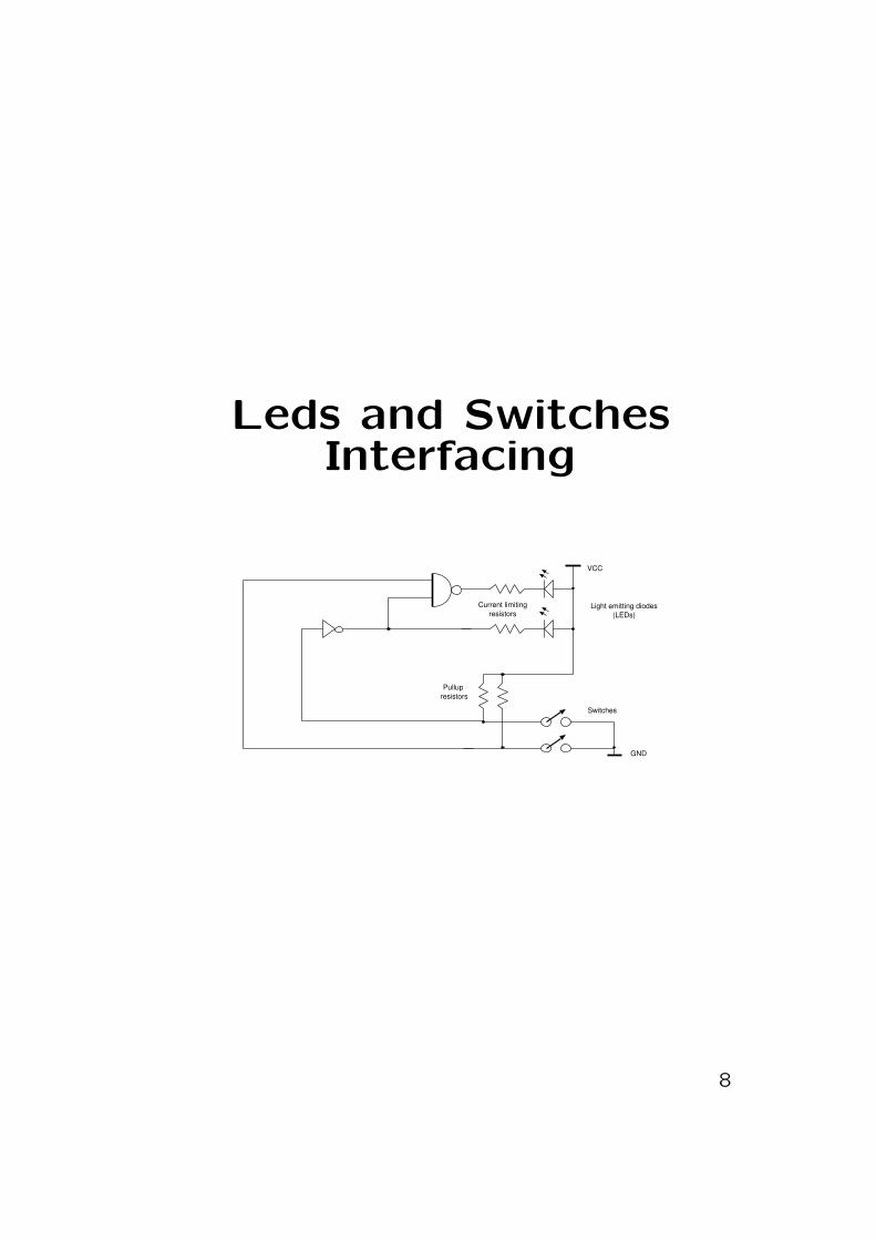
Leds and SwitchesInterfacing
GND
VCC
Pullup resistors
Light emitting diodes(LEDs)
Switches
Current limitingresistors
8

Bistable Revision
The bistable is the most basic electronic store
for one bit.Vo
Vin
VoVin Metastable Point
Adding a pair of inputs makes an RS latchQ
Q
s
r
S
R Q
qbs
r
9

Flip-Flop Revision
Making a transparent latch from an RS latch:
G
enable
D Q
Q
enable
D
G
D Q
qbs
r
db
Putting two together we get the D-type:D
Clock
QX
Y
SlaveMaster
clock
QDD Q
A more optimal circuit:Q
Clock
D
X
Y
Slave
MasterQD
D Q
In this course, we go upwards from the D-typetowards systems.
10

Adding a Clock Enable andSynch Reset
Adding a clock enable
D
Clock
Data in
Q Output
Clock enable
DData in Q Output
Clock enable
Clock
CE
LOGIC SYMBOL AN EQUIVALENT CIRCUIT
1
0
always @(posedge clk) q <= (clock_en) ? data_in: q;
alternatively
always @(posedge clk) beginif (clock_en) q <= data_in;...end
Adding a Synchronous Reset
D
Clock
Data inQ OutputDData in Q Output
Synchronous Reset
Clock
SR
LOGIC SYMBOL AN EQUIVALENT CIRCUIT
1
0
Synchronous Reset
0
always @(posedge clk) q <= (sr) ? 0:data_in;
11

A Broadside Register
Broadsideregister
N N
Clock
QD
D
Clock
D
D
D
Q0
Q1
Q2
Q(N-1)
D0
D1
D2
D(N-1)
A broadside register of N bits is made out of
N D-types with a commoned clock input. It
can hold 2N different values.12

A Broadside Register -Verilog
Broadsideregister
N N
Clock
QD
D
Clock
D
D
D
Q0
Q1
Q2
Q(N-1)
D0
D1
D2
D(N-1)
parameter N = 8;
reg [N-1:0] br_q;
always @(posedge clk) begin
br_q <= data_in;
end
13

A broadside two-to-onemultiplexor
MUX2N
NN
Select
DT
DFY
Select
Y0
Y1
Y(N-1)
DT0
DF0
DT1
DF1
DT(N-1)
DF(N-1)
wire [N-1:0] Y, DT, DF;
assign Y = (Select) ? DT: DF;
14

Shift Registers
An n-bit shifter
D Q D Q D QSerial in
Clock input
Q[0] Q[1] Q[n-1]Q[2]
DSerial in
Clock input
Q
n
Adding a parallel load
D QSerial in
Clock input
Q[0] Q[1]
PLParallel Load
Clock input
Q
n
P
n
DSerial in
D Q D Q
Q[n-1]
Parallel Load
P[0] P[1] P[n-1]
parameter N = 8;
reg [N-1:0] Q;
always @(posedge clk) begin
Q <= (PL) ? P: (Q << 1) | D;
end
15
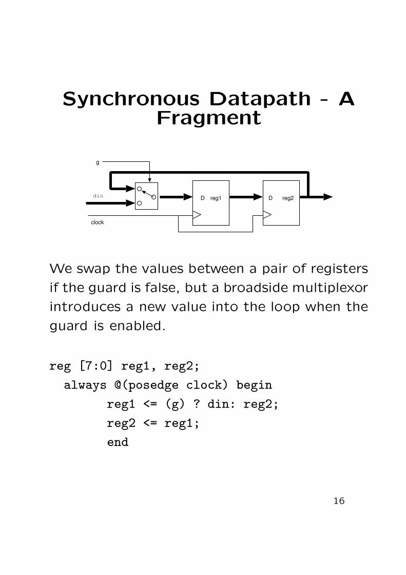
Synchronous Datapath - AFragment
din D reg1
clock
D reg2
g
We swap the values between a pair of registers
if the guard is false, but a broadside multiplexor
introduces a new value into the loop when the
guard is enabled.
reg [7:0] reg1, reg2;
always @(posedge clock) begin
reg1 <= (g) ? din: reg2;
reg2 <= reg1;
end
16

A Dual-Port Register File
Write Address
Data in Data out A
clock
N N
A
Read Address B
A
Read Address A
A
Data out B
NWrite Enable
(wen)
// Verilog for a dual-read ported register file.input [3:0] write_address, read_address_a,
read_address_b;reg [7:0] regfile [15:0]always @(posedge clk) begin
if (wen) regfile[write_address] <= din;end
wire [7:0] data_out_a = regfile[read_address_a];wire [7:0] data_out_b = regfile[read_address_b];
Ex: Draw out the full circuit at the gate level!
17

Read/Write Memory (RAM)
Address In
Data Bus
Enable Input(active low)
Valid dataHigh-ZHigh-Z
Read Cycle - Like the ROM
Write Cycle - Data stored internally
Read or writemode select
Address In
Data Bus
Enable Input(active low)
Data must be validhere to be stored.
High-Z
High-Z
Read or writemode select
Data In and Out
Address In
Enable Input(active low)
E
Addr
Data
N
A
RAMR/WbRead or write
mode select
Each data bit internally stored in an RS latch.
18

Read Only Memory (ROM)
The ROM takes A address bits named A0 to A<A-1> and produces datawords of N bits wide. For example, if A=5 and D=8 then the ROMcontains 2**5 which is 32 locations of 8 bits each. The address linesare called A0, A1, A2, A3, A4 and the data lines D0, D1, ... D7
Address In
Data Out
Enable Input(active low)
Valid dataHigh-ZHigh-Z
The ROM’s outputs are high impedance unless the enable inputis asserted (low). After the enable is low the
output drivers turn on. When the address has been stablesufficiently long, valid data from that address comes out.
The ROM contentsare placed inside during
manufacture or fieldprogramming.
Data Out
Address In
Enable Input(active low)
E
Addr
Data
NA
ROMPROM
orEPROM
Access Time
Ouput Turnon Time
MASKED PROGRAMMED means contents in-
serted at time of manufacture.
FLASH PROM uses static electricity on float-
ing transistor gates.
19

Non-volatile Technologies
Name Persistence Read Speed Write RateRAM Volatile Same as SRAM Same as SRAM
BB-RAM Non-volatile Same as SRAM Same as SRAMMask PROM Non-volatile Same as SRAM Not possible
EPROM Non-volatile Same as SRAM 10 us/byteSn-W PROM Non-volatile Same as SRAM 10 us/byte
EAROM Non-volatile Same as SRAM 10 us/byte
Name Erase Time CommentRAM not needed
BB-RAM not needed Battery LifeMask PROM Not Possible
EPROM 20 Mins Needs UV windowSn-W PROM Not possible
EAROM 100 ms/block write cycle limit
20
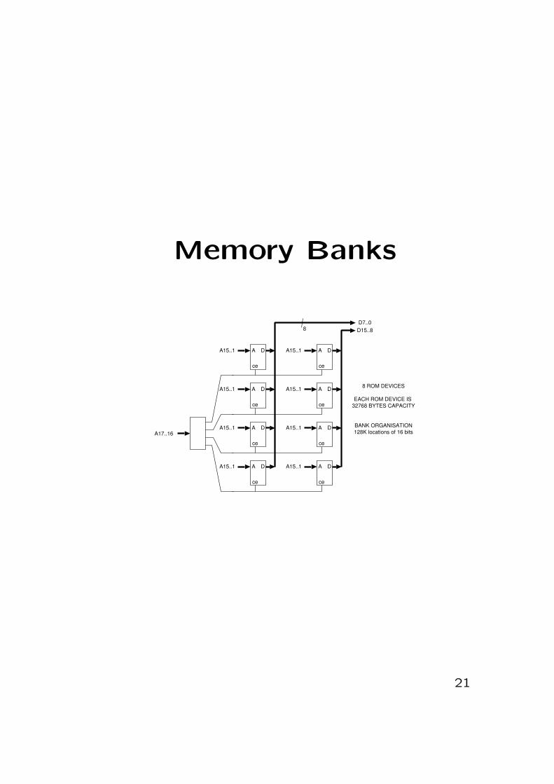
Memory Banks
A15..1 A15..1
A15..1 A15..1
A15..1 A15..1
A15..1 A15..1
A17..16
8D7..0D15..8
ce
A D
ce
A D
ce
A D
ce
A D
ce
A D
ce
A D
ce
A D
ce
A D
8 ROM DEVICES
EACH ROM DEVICE IS 32768 BYTES CAPACITY
BANK ORGANISATION128K locations of 16 bits
21

GD GD GD GD GD GDData
Address Input
Binary to unary decoder
WE*
CE*
outputenable
G
QD
Transparent latchschematic symbol
D
G
Q
Transparent latch implemented from gates.
Unlike the edge-triggered flip-flop, the transparent latchpasses data through in a transparent way when its enable
input is high. When its enable input is low, the output staysat the current value.
22

Synchronous FIFO Memory
FIFO Queue
N N
DIN
WRCLK
WREN RDEN
RDCLK
HF FFEF
DOUT
23
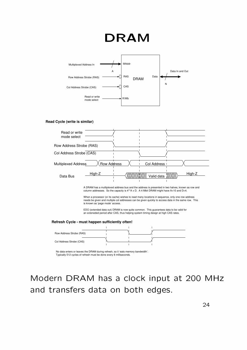
DRAM
Refresh Cycle - must happen sufficiently often!
A DRAM has a multiplexed address bus and the address is presented in two halves, known as row andcolumn addresses. So the capacity is 4**A x D. A 4 Mbit DRAM might have A=10 and D=4.
When a processor (or its cache) wishes to read many locations in sequence, only one row addressneeds be given and multiple col addresses can be given quickly to access data in the same row. Thisis known as ‘page mode’ access.
EDO (extended data out) DRAM is now quite common. This guarantees data to be valid foran exteneded period after CAS, thus helping system timing design at high CAS rates.
Multiplexed Address
Data Bus Valid dataHigh-ZHigh-Z
Read Cycle (write is similar)
Read or writemode select
Row Address Col Address
Row Address Strobe (RAS)
Col Address Strobe (CAS)
Row Address Strobe (RAS)
Col Address Strobe (CAS)
No data enters or leaves the DRAM during refresh, so it ‘eats memory bandwidth’.Typically 512 cycles of refresh must be done every 8 milliseconds.
Data In and Out
Multiplexed Address In
Row Address Strobe (RAS) RAS
MAddr
Data
N
A
DRAM
R/WbRead or writemode select
Col Address Strobe (CAS) CAS
Modern DRAM has a clock input at 200 MHz
and transfers data on both edges.
24

Crystal oscillator clocksource
33pF
Ground
33pF
1M
RC oscillator clock source
Ground
C
R Vo
Vin
SchematicSymbol
Shmitt Inverter
25

Clock multiplication anddistribution
VCO
Clock distribution H tree
1000MHz
100 MHz
Divide 10
Externalclockinput
PLL Circuit
Outsidethe chip
Insidethe chip
H tree layout
Power-on reset
Ground
C
R
Reset output
Supply
Active low
Vo
Vi
26

Driving a heavy current orhigh-voltage load
Ground
Control input
High Voltage Supply
BackEMF
protectiondiode
PowerMOSFT
transistor
Load may bedirectly connectedor driven through amechanical relay
Transistor active area could be 1 square cen-
timeter.
27

Debouncer circuit for adouble-throw switch
A
B
Output
Output
A
B
Gnd
+5Volt supply rail
PullupResistors
Bounces
Switch
28

ALU and Flags RegisterFunction Code
4
N
N
N
Carry In
ALU
A-input
B-input
Output
C
N
Z
V
Flags Clock
Flags register
input [7:0] A, B, fc;output [7:0] Y;output C, V, N, Z;
always @(A or B or fc)case (fc)0: { C, Y } = { 1’b0, A }; // A1: { C, Y } = { 1’b0, B }; // B2: { C, Y } = A+B; // A+B3: { C, Y } = A+B; // A+B4: { C, Y } = A+B+cin; // A+B+Carry in5: { C, Y } = A-B // and so on
...endcase
assign Z = (Y == 0); assign N = y[7];
29

ALU and Register File
FunctionCode
4
8
Carry In
8 bitALU
A-input
B-input
Output
4 bitcounter
Register file16 registers
of 8 bits
4
A
8
D
Carry Out
QDin
8
B
A
Clock source
FUNCTION GEN
Zerodetect
8
FUNCTION GEN
for F code
for A input
An example structure using an ALU and regis-
ter file.
Ex: Program the ROM function generators to
make one large counter out of the whole reg-
ister file.30

Multiplier
Flash multiplier - combinatorial implementa-
tion (e.g. a Wallace Tree).n
m
n+m
n+m-1 if signed
Sequential Long Multiplication
RA=ARB=BRC=0while(RA>0){
if odd(RA) RC=RC+RB;RA = RA >> 1;RB = RB << 1;
}
31

Micro Architecture for aLong Multiplier
Ready
Clock input
C16B
Start
D Q
A
8
D Q C
8
8
ARA
RC
/2D Q
8B
RB
x2
x
y
fc
p
ReadyStartfcp
yx
FSM
8
16
bit 0 q
q
16
8
32

Booth’s multiplier
Booth does two bits per clock cycle:
(* Call this function with c=0 and carry=0 to multiplyx by y. *)
fun booth(x, y, c, carry) =if(x=0 andalso carry=0) then c else
let val x’ = x div 4val y’ = y * 4val n = (x mod 4) + carryval (carry’, c’) = case (n) of
(0) => (0, c)|(1) => (0, c+y)|(2) => (0, c+2*y)|(3) => (1, c-y)|(4) => (1, c)
in booth(x’, y’, c’, carry’)end
Ex: Design a micro-architecture consisting of
an ALU and register file to implement Booth.
Design the sequencer too.
33

Logic Symbol
Internal Structure Block Diagram
Address
DataN
A
System Clock
Reset Input
Interrupt RequestOperationRequest
Read/Notwrite
Wait
I
W
R/Wb
Opreq
R
Microprocessor
Operation Request
Read/notwrite
Data Bus
Address Bus
Bus Control
Clock
ALU
MUX
Addresses
Dual PortRegister
File
Write
Execution Unit
Control Unit
InstructionRegister
InstructionDecoder
Control Wires ToAll Other Sections
Mux 2
ProgramCounter
Execution addressincrementor
Clock
ClockClock
MUX2
Function code Load or Store
System Clock
ResetPC
Reset
OPERAND EAIR
34

D Q
GND
VCCBroadside latch
Broadsidetri-state
Microprocessor
D0
D1
D2
Part of data bus
Part of address bus
A12
A13
A14
A15
R/Wbar
OPREQ
Pullup resistors
Light emitting diodes(LEDs)
Write to leds
Read from switches
D3
D4
D5 Switches
Example of memory address decode and simple
LED and switch interfacing for programmed IO
(PIO) to a microprocessor.
35

A D8/A16 Computer
ControlUnit
ExecutionUnit
+ ALU
Memory
Static RAM
16 kByte
UART Serial Port
Address bus(16 bits)
Data bus(8 bits)
(Micro-)Processor
Rs232 Serial Connection
Register File(including PC)
D0-7
D0-7
D0-7
Clock Reset
R/Wb
Memory Mapdecoder circuit
Often a ‘PAL’single chip device.
A15
A14
A13
R/WbR/Wb
A0-13
Enb
Enb
Enb
1 K Byte ROMRead Only Memory
A0-9
A0-2
R/WbR/Wb
ROM_ENABLE_BAR
UART_ENABLE_BAR
RAM_ENABLE_BAR
D0-7
36

Memory Address Mapping
ROM /CS
RAM /CS
UART /CS
A14
A15
------- ----- -----------------------Start End Resource------- ----- -----------------------0000 03FF EPROM0400 3FFF Unused images of EPROM4000 7FFF RAM8000 BFFF UnusedC000 C001 Registers in the UARTC002 FFFF Unused images of the UART------- ----- -----------------------
module address_decode(abus, rom_cs, ram_cs, uart_cs);input [15:14] abus;output rom_cs, ram_cs, uart_cs);
assign rom_cs = (abus == 2’b00); // 0x0000assign ram_cs = (abus == 2’b01); // 0x4000assign uart_cs = !(abus == 2’b11);// 0xC000
endmodule
37

PC Motherboard, 1997 vintage
SIMM 4
SIMM 3SIMM 2SIMM 1
COM1
COM2
USB IDE-1
IDE-2
Floppy
BIOS ROM
PentiumCPU
CACHE RAMPSU
KYBD
PCI1
PCI2
PCI3
ISA16 BITSLOTS BATTERY
PRINTER CacheControl
IDE &Floppy
Generalglue
Clock Regulator
Main memory DRAM
38

Pa
ralle
lP
ort
Address
Data
device select/cs
Strobe
Read/Writebarr/wbar
Acknowledge
Parallel Data
Busy
D25 Parallel (Centronix) Port
Strobe_bar
Acknowledge
Parallel Data
Busy
Valid Data For Transfer To Peripheral Device
Ready for next data
Parallel Port Interface Logic
Flow control: New data is not sent whilethe busy wire is high.
CPUBUSSIDE
39
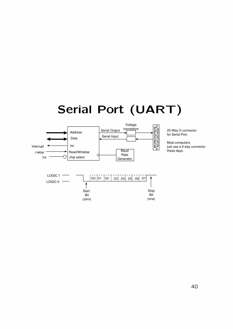
Serial Port (UART)
DO D1 D2 D3 D4 D5 D6 D7LOGIC 1
LOGIC 0
Start Bit
(zero)
StopBit
(one)
Address
Data
chip select/cs
Serial Input
Serial Output
BaudRate
Generator
Read/Writebarr/wbar
Interrupt Int
Voltageconvertors 25-Way D connector
for Serial Port.
Most computersjust use a 9 way connectorthese days.
40

Keyboard and/or PS/2 port+5 Volt Fuse
Ground
Clock wire
Data Wire
Power wire
Ground wires
PS/2Connector
1
2
34
5
6
PS/2 Keyboard/Mouse Cable 1. Clock 2. Ground 3. Data 4. Spare 5. Power +5Volts 6. Spare
Open drain/collector wiring using two signalling
wires.
The 1394 Firewire and USB ports are essen-
tially the same as PS2 at the physical layer.
41

Ethernet
MAC
PHY
TX-DATATX-CLK
RX-DATARX-CLKCS/COL
RX QUEUE
TX QUEUERJ45 Socket
(4 of 8 pins used)
TransformersProcessor BusAddress
Data
device select/cs
Read/Writebarr/wbar
IRQinterrupt
42

Canonical Synchronous FSM
FSM
Clock
Mealy Outputs
Inputs
D
Clock
D
D
D
Q0
Q1
Q2
Moore Outputs
LOOP-FREE COMBINATORIAL LOGIC BLOCK
I0
I1
I(M-1)
M
I2
CURRENT STATE FEEDBACK
STATE FLOPS
LOOP-FREE COMBINATORIAL LOGIC BLOCK
LOOP-FREE COMBINATORIAL LOGIC BLOCK
Moore Outputs
Mealy Outputs
Inputs
FSM = { Set of Inputs, Set of states Q, Transiton function D)
An initial state can be jumped to by terming one of the inputs a reset.
An accepting state would be indicated by a single Moore output.
In hardware designs, we have multiple outputs of both Mealy and Moore style.
43

Canonical Logic Array
Inputs Outputs
OR (sum)array
AND(product)
Array
44
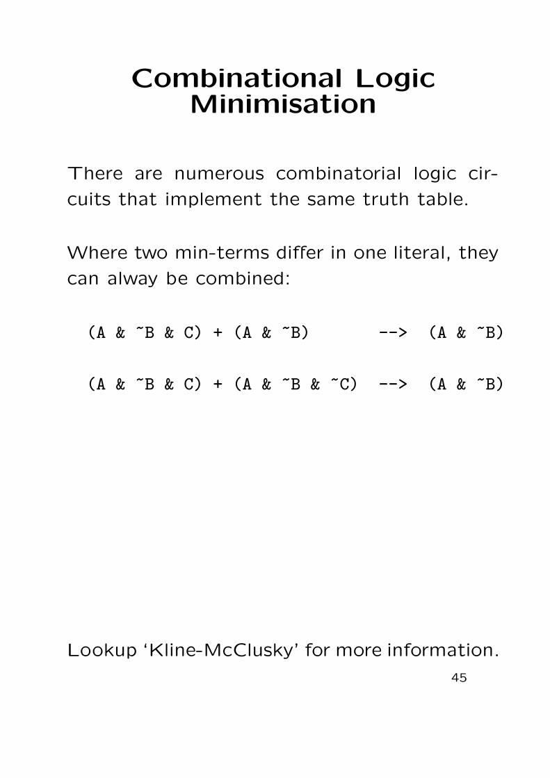
Combinational LogicMinimisation
There are numerous combinatorial logic cir-
cuits that implement the same truth table.
Where two min-terms differ in one literal, they
can alway be combined:
(A & ~B & C) + (A & ~B) --> (A & ~B)
(A & ~B & C) + (A & ~B & ~C) --> (A & ~B)
Lookup ‘Kline-McClusky’ for more information.
45

Karnaugh Maps are convenient to allow the hu-man brain to perform minimisation by patternrecognition.
(A & ~C) + (A & B) + (B & C) -->
(A & ~C) + (B & C)A
B
C
Often, there are don’t care conditions, thatallow further minimisation. Denote with an Xon the K-map:
A
B
CX
(A & ~C) + (A & B) + (B & C) -->
A + (B & C)
Lookup ‘ESPRESSO’ for more information.
46

Sequential LogicMinimisation
A finite state machine may have more statesthan it needs to perform its observable func-tion.
1
1
00
0
2
2
2
1
1
A Moore machine can be simplified by the fol-lowing procedure
1. Partition all of the state space into blocks ofstates where the observable outputs are the samefor all members of a block.
2. Repeat until nothing changes (i.e. until it closes)For each input setting:
2a. Chose two blocks, B1 and B2.2b. Split B1 into two blocks consisting of those
states with and without a transition from B2.2c. Discard any empty blocks.
3. The final blocks are the new states.
47

Timing Specifications
Clock
Data inD Q oiutputQ
Q oiutput
Data in
Clock
Hold time
Propagation delay
Setup time
48

Typical Nature of a CriticalPath
Clock
A
B
C
DSetup
Margin
Period = 1/F
Clock
D Q
D Q
AB
CD
Clock speed can be increased while margin is
positive.
49

Johnson counters
D Q3D Q2D QA
Clock
Q1 Q2 Q3
Q1 Q2 Q3
50

Pip
elin
ing
Data inD Q
D Q
D Q
D Q
D Q
D Q
Synchronous global clock signal
Another input
Yet another input
An output
Yet another output
Another output still
Large loop-free combinatorial logic function
Data inD Q
D Q
D Q
D Q
D Q
D Q
Synchronous global clock signal
Another input
Yet another input
An output
Yet another output
Another output still
Loop-free combinatorial logicfunction - second half
Desired logic function
Desired logic function - pipelined version.
D Q
D Q
D Q
D Q
Loop-free combinatorial logicfunction - first half
51

Cascading FSMs
FSM
Mealy OutputsInputs
Moore Outputs
FSM
Mealy Outputs
Moore Outputs
FSM
Inputs
Clock
Moore
Mealy
Inputs
52

How Not To Do It
D Q D Q D Q D Q Shift Register
D QD QD QD QD Q
Five Bit BroadsideRegister
Divideby 5
counter
Parallel data out
Serial in
Clock input
An example that uses (badly) a derived clock:
a serial-to-parallel converter
reg [2:0] r2;always @(posedge clock) r2 <= (r2==4)?0:r2+1;wire bclock = r2[2];
reg [4:0] shift_reg;always @(posedge clock)
shift_reg <= serial_in | (shift_reg << 1);
reg [4:0] p_data;always @(posedge bclock) p_data <= shift_reg;
Care is needed when gating clocks.
53

A Gated Clock
D
Master Clock
D
Synchronous subsystem requiringgated clock
J
K
EnablebarEnable expression
OR’ing with a negated enable works cleanly.
Use this to power down a sub-section of a chip
or when synchronous clock enable becomes costly.
54

Clock Skew
D Q
Delay
D Q
Delay
D Q
Delay
Data input Data outputQA QB
Clock
a) A three-stage shift register with some clock skew delays.
D Q
Delay
Data input QB
b) System interconnection with clock skews
Delay
c) A solution for serious skew and delay problems ?
D Q
Delay
QBDelay
D Q
Delay
QBDelay
Clock
D Q
Delay
Data input QBDelay
D Q
Delay
QBDelay
D Q
Delay
QBDelay
Clock
55
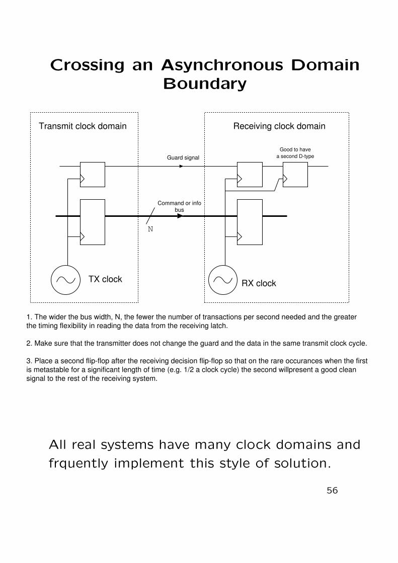
Crossing an Asynchronous DomainBoundary
Receiving clock domainTransmit clock domain
TX clock RX clock
Guard signal
Command or infobus
N
Good to havea second D-type
1. The wider the bus width, N, the fewer the number of transactions per second needed and the greaterthe timing flexibility in reading the data from the receiving latch.
2. Make sure that the transmitter does not change the guard and the data in the same transmit clock cycle.
3. Place a second flip-flop after the receiving decision flip-flop so that on the rare occurances when the first is metastable for a significant length of time (e.g. 1/2 a clock cycle) the second willpresent a good clean signal to the rest of the receiving system.
All real systems have many clock domains and
frquently implement this style of solution.
56

Dicing a wafer
(Chips are not always square)
57

A chip in its package, ready forbond wires
DIE
PIN
PACKAGEBOND PADCAVITY
IO and power pads
Connectionsto and fromcore logic
Pad powersupply
PadElectronics
SupplyPad
GroundRail
SignalBondPad
Edge of Die
Power Rail
GroundPad
CORE AREA
58

Die cost example
Area Wafer dies Working dies Cost per working die2 9000 8910 0.563 6000 5910 0.854 4500 4411 1.136 3000 2911 1.729 2000 1912 2.62
13 1385 1297 3.8519 947 861 5.8128 643 559 8.9542 429 347 14.4063 286 208 24.0094 191 120 41.83
141 128 63 79.41211 85 30 168.78316 57 12 427.85474 38 4 1416.89
59

A taxonomy of ICs
StandardParts
Digital Integrated Circuits
ASICs FieldProgrammable
Parts
FPGA
e.g.
XilinxSpartan
ArrayLogic
(PALs)
e.g.22V10Commodity
Parts
SOCFPGAs
e.gAltera
Excalibur
SemiCustom
StandardCell
FullCustom
SemiCustom
StandardCell
FullCustom
e.g.LAN
InterfaceControllere.g.
Memories
RarelyUsed
e.g.Toys
60

Field Programmable Gate Arrays
CLB
SWITCHMATRIX
CLB
SWITCHMATRIX
CLB
SWITCHMATRIX
CLB
SWITCHMATRIX
CLB
SWITCHMATRIX
CLB
SWITCHMATRIX
CLB
SWITCHMATRIX
CLB
SWITCHMATRIX
CLBCLB CLB
CLB
SWITCHMATRIX
CLB
CLB
SWITCHMATRIX
SWITCHMATRIX
Bondpad
IOB
Bondpad
IOB
Bondpad
IOB
Bondpad
Bondpad IOB
Bondpad IOB
Bondpad IOB
Edge of die
61

A configurable logic block for alook-up-table based FPGA
Generalinputs
Combinatorialfunctiongenerator
D Q
D Q
Clock input
First output
Second Output
Programmable multiplexers
This CLB contains one LUT and two D-type’s.
The output can be sequential or combinational.
Seven LUT inputs: 27 = 128
The LUT can be a RAM of 128 locations of
two bits.
62
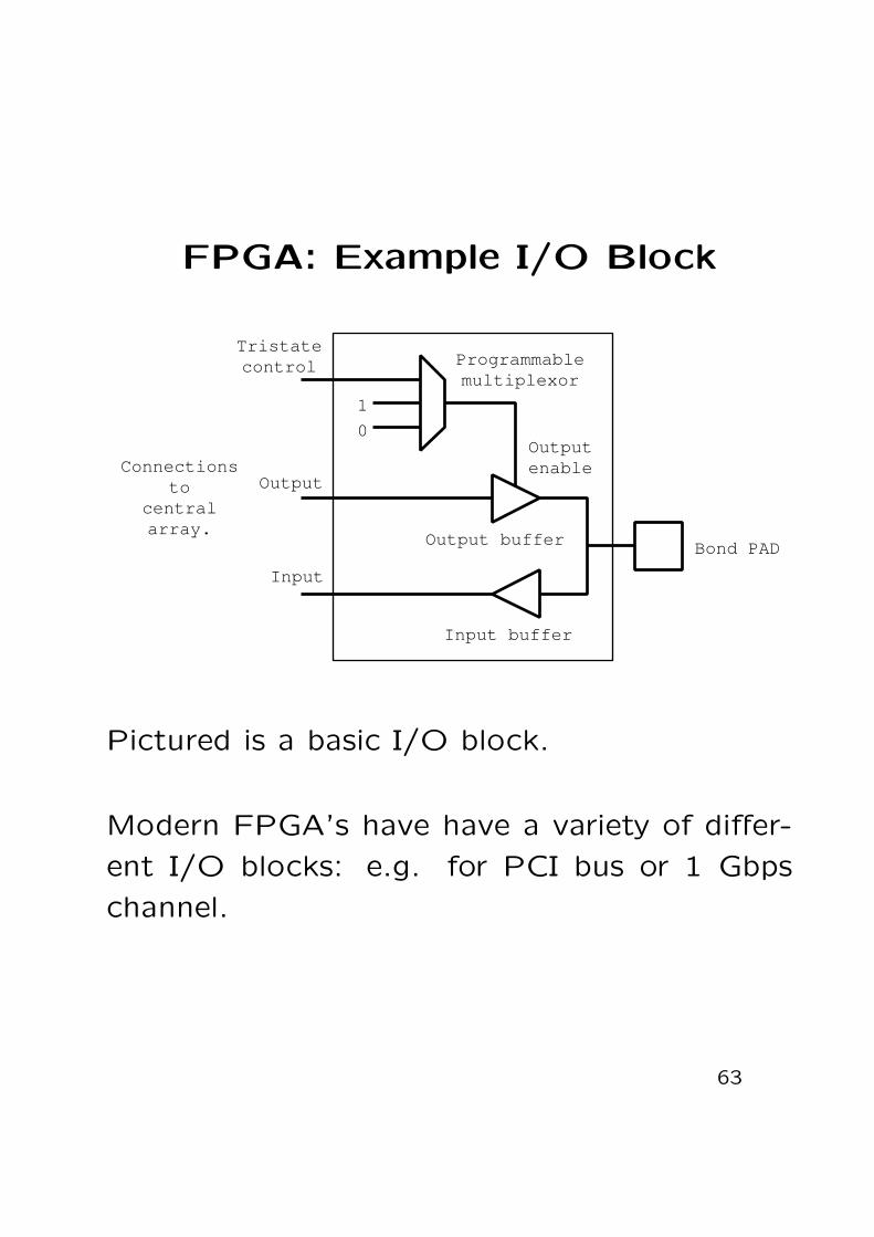
FPGA: Example I/O Block
Bond PAD
Input buffer
Input
Output
Tristatecontrol
Outputenable
Programmablemultiplexor
1
0
Output buffer
Connectionsto
centralarray.
Pictured is a basic I/O block.
Modern FPGA’s have have a variety of differ-
ent I/O blocks: e.g. for PCI bus or 1 Gbps
channel.
63

Powersupply
pin
Clocksignal
Clockinput
Generalpurposeinputs
Productline
Termline
Outputpad
(can alsobe input).
Outputenable
product line
Groundpin.
The crosspoints in
these shadedregions
areprogrammable
points
Macro-cell
Macro-cell
Macro-cell
1
2
3
4
5
6
7
8
910
11
12
13
14
15
16
17
64

Contents of the PAL macrocell
Inputbuffer
Clock Net
I/O Pad
Tristateoutput pad
Programmablemultiplexor
D-typeflip-flop
D QMain inputS-of-P
Output enableterm
Feedback toarray
65

Example programming of a PALshowing only fuses for the top
macrocell
pin 16 = o1;pin 2 = a;pin 3 = b;pin 4 = c
o1.oe = ~a;o1 = (b & o1) | c;
-x-- ---- ---- ---- ---- ---- ---- (oe term)--x- x--- ---- ---- ---- ---- ---- (pin 3 and 16)---- ---- x--- ---- ---- ---- ---- (pin 4)xxxx xxxx xxxx xxxx xxxx xxxx xxxxxxxx xxxx xxxx xxxx xxxx xxxx xxxxxxxx xxxx xxxx xxxx xxxx xxxx xxxxxxxx xxxx xxxx xxxx xxxx xxxx xxxxxxxx xxxx xxxx xxxx xxxx xxxx xxxxx (macrocell fuse)
66
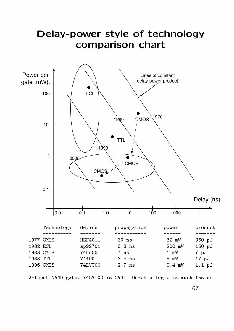
Delay-power style of technologycomparison chart
Delay (ns)
Power pergate (mW).
0.1 1.0 10 100 1000
1
10
100 ECL
TTL
CMOS
Lines of constantdelay-power product
1980
1990
2000
0.01
0.1
CMOS
1970CMOS
Technology device propagation power product---------- ------- ----------- ------ -------
1977 CMOS HEF4011 30 ns 32 mW 960 pJ1982 ECL sp92701 0.8 ns 200 mW 160 pJ1983 CMOS 74hc00 7 ns 1 mW 7 pJ1983 TTL 74f00 3.4 ns 5 mW 17 pJ1996 CMOS 74LVT00 2.7 ns 0.4 mW 1.1 pJ
2-Input NAND gate. 74LVT00 is 3V3. On-chip logic is much faster.
67

Logic net with tracking and inputload capacitances
Parasiticinput
capacitance
Track to substratecapacitance proportional
to total track length (area)
DrivingGate
Drivengates
68
An example cell from amanufacturer’s cell library
Simulator/HDL Call
NAND4 Standard Cell
4 input NAND gate with x2 drive
Schematic Symbol
NAND4X2(f, a, b, c, d);
ELECTRICAL SPECIFICATIONSwitching characteristics : Nominal delays (25 deg C, 5 Volt, signal rise and fall 0.5 ns)
Inputs Outputs
O/P Falling O/P Rising
ABCD
FFFF
(ps) ps/LU ps ps/LU
142161165170
37373737
198249293326
33333334
Min and Max delays depend upon temperature range, supply voltage, input edge speed and processspreads. The timing information is for guidance only. Accurate delays are used by the UDC.
: (One load unit = 49 fF)
Parameters
Input loading
Drive capability
Pin
abcd
f
Value
2.12.12.12.0
35
Load units
Load units
Units
a
b
c
d
f
Logical Function
F = NOT(a & b & c & d)
Library: CBG0.5um
X2
CELL PARAMETERS
69

Current digital logic technologies
1994 - First 64 Mbit DRAM chip.
• 0.35 micron CMOS
• 1.5 micron2 cell size (64E6 × 1.5 um2 = 96E6)
• 170 mm2 die size
1999 - Intel Pentium Three
• 0.18 micron line size
• 28 million transistors
• 500-700 MHz clock speed
• 11x12 mm (140 mm2) die size
2003 - Lattice FPGA
• 1.25 million use gate equivs
• 414 Kbits of SRAM
• 200 MHz Clock Speed
• same die size.
See www.icknowledge.com
70

Design partitioning: TheCambridge Fast Ring
8
8
8
DRAM
CMOSCHIP
(StandardPart)
ECLCHIP
Isolatingtransformers
RingConnector
VCO(analogue)
InterruptPAL
Standard databuffers
Address PAL
HostBus
12.5 MHz
100 MHz
Designed in 1980.
ECL Chip 100 MHz, bit serial.
CMOS Chip 12.5 MHz, byte-wide data.
71

A Basic Micro-Controller
Microprocessor(8 bit generally)
RAM(e.g. 2 Kbytes)
OTPEPROM
(e.g.
8 Kbytes)
ClockOsc
Power Upreset
Programmable IOCounters andTimers UART
I/O wires OR external bus
Reset capacitorClock
Serial TX and RX
Internal A and D busses
Introduced 1989-85.
Such a micro-controller has an D8/A16 architecture and
would be used in a mouse or smartcard.
72

De
sign
pa
rtition
ing
:A
Mo
de
m.
Telephoneline interface
Off-hook relay
Isolationtransformer A-to-D
D-to-A
MainDSP
processor
Single-chipprocessor
RS-232line drivers
Computerinterface
Led indicators
Power supplyconditioning
Ringdetector
DSPROM
DSPRAM
Directionalisolator
NV-RAM
DC powerinput
In1
98
0w
eu
sed
am
icro
co
ntro
ller
with
ex
tern
al
DS
Pc
om
po
ne
nts.
73

Design partitioning: A MiniatureRadio Module
DAC
CarrierOscillator2.4 GHzMicrocontroller
BasebandModem
Antenna
DataInterfaces
RFAmps
IFAmps
ADC
FLASHmemory chip
Digital Integrated Circuit
Analog (RF) Integrated Circuit
Linedri-vers
HopController
www.bluetooth.orgwww.csr.com
Multi-chip module or mini PCB
RAM
Introduced 1998.
74

19
98
:A
Pla
tform
Ch
ip:
D3
2/
A3
2tw
ice
!
Ethernetblock
USBblock
UART(s)
PCI businterface
I/OProcessor
ARM
DSPprocessor
Special peripheralfunction
DRAMInterface
DRAM
Cache
LocalRAM
for DSP
LocalIO/BUS
Misc Peripheralson the same PCB
CounterTimerBlock
AtoDchannels
DtoAchannelsBus
Bridge
FIFO Bus Bridge
DRAMInterface
10/100/1GEthernet
USB
Serial lines
PCI Bus
I/O pinsfor specialperipheralfunction
Analog Input
Analog Output(e.g.) L/R audio
PSUand test logic
etc
ControlProcessor
ARM
Cache
CounterTimerBlock
BusBridge
Microcontollerstyle GPIO
DSPprocessor DMA
Controller
A D R/W
75

System on a Chip = SoC design.
Our platform chip has two ARM processors and two DSP proces-sors. Each ARM has a local cache and both store their programsand data in the same offchip DRAM.
The left-hand-side ARM is used as an I/O processor and so isconnected to a variety of standard peripherals. In any typical ap-plication, many of the peripherals will be unused and so held in apower down mode.
The right-hand-side ARM is used as the system controller. It canaccess all of the chip’s resources over various bus bridges. It canaccess off-chip devices, such as an LCD display or keyboard via ageneral purpose A/D local bus.
The bus bridges map part of one processor’s memory map into thatof another so that cycles can be executed in the other’s space,allbeit with some delay and loss of performance. A FIFO busbridge contains its own transaction queue of read or write oper-ations awaiting completion.
The twin DSP devices run completely out of on-chip SRAM. SuchSRAM may dominate the die area of the chip. If both are fetchinginstructions from the same port of the same RAM, then they hadbetter be executing the same program in lock-step or else havesome own local cache to avoid huge loss of performance in buscontention.
The rest of the system is normally swept up onto the same piece
of silicon and this is denoted with the ‘special function periperhal.’
This would be the one part of the design that varies from product
to product. The same core set of components would be used for all
sorts of different products, from iPODs, digital cameras or ADSL
modems.

LEDs wired in a matrix to reduceexternal pin count
A
B
C
D
E
P Q R S T
76

IRH
an
dse
tIn
tern
al
Circ
uit
Battery
Scan multiplexed keyboard
Single chipcontaining
all semiconductors
Clock capacitor Infra-redtransmitdiodes
+
-
77

Scan multiplex logic for an LEDpixel-mapped display
Pixel
RAMSCAN
MULTIPLEXEDDISPLAYMATRIX
N bitCOUNTER
BINARY to UNARYDECODER
Row
Addr
Data lilines(zero for on)
CLOCK
A
D
2^N col lines
One col line islogic one at a time.
You made one of these in the Ia H/W classes.
78

Addition of psudo dual-portinglogic
PixelRAM
SCANMULTIPLEXED
DISPLAYMATRIX
N bitCOUNTER
BINARY to UNARYDECODER
Row
A
D
Broadsidetri-statebuffer
Writedata
Write address
WE
Writestrobebar
MUX2 N
You did this too!79

Use of a ROM as a functionlook-up table
A to Dconvertor
Look-up table ROM
D to Aconvertor
16 16
65536 by 16 ROM
Sample clock 44.1 kHz
12 inch speakers
Amplifer
A D
The ROM contains the exact imperfections of
a 1950’s valve amplifier.
80

Use of an SRAM to make the delayrequired for an echo unit
A to Dconvertor
D to Aconvertor
16 16
Amplifer
A
D
Static RAM65536 by 16 bits16 bit
synchronouscounter 16
RAMWE
RAMOE
ADOE
Timing generatorcircuit
ADOE
RAMWE
RAMOE
Derived clock, 44.1 kHz
88.2 kHz
Read cycle Write cycle Read cycle
Clock 88.2
Clock 44.1
RAMWE
RAMOE
Counter Output N-1 N N+1
RAM data pins Old sample replay New sample write
81

Merge unit block diagram
DO D1 D2 D3 D4 D5 D6 D7
LOGIC 1
LOGIC 0
Start Bit
(zero)
StopBit
(one)
Bit spacing is reciprocal of31.25 kbaud, which is 32 microseconds.
+
5V VCC
-
Logic leveloutput
Open collectorbuffer
220R
220R
GND
5V VCC
LED
Photo-transistor
+
-
Logic level input220R
GND
5V VCC
LED
Photo-transistor
+
-
Logic level input220R Mergedmidi output
Midi inputone
Midi inputzero
Midi merge
functionto be
designed
Clock1 MHz
module MERGER(out, in0,in1, clk);
MIDI serial data format
9n kk vv (note on)
8n kk vv (note off)
9n kk 00 (note off with zero velocity)
82

MIDI merge unit internal functional units
Serial to par
Removestatus
FIFO Queue
Serial to par
Removestatus
Queue
Par toserial
Insertrunningstatus
Queue
Megercore
function
Midi In 0
Midi In 1
Mergedmidi output
8 24
8 24
8 24
24
24
24
83

The serial to parallel converter:
input clk;output [7:0] pardata; output guard;
The running status remover:
input clk;input guard_in; input [7:0] pardata_in;output guard_out; output [23:0] pardata_out
For the FIFOs:
input clk;input guard_in; input [7:0] pardata_in;input read; output guard_out; output [23:0] pardata_out;input read; output guard_out; output [23:0] pardata_out;
For the merge core unit:
input clk;input guard_in0; input [23:0] pardata_in0; output read0;input guard_in1; input [23:0] pardata_in1; output read1;output guard_out; output [23:0] pardata_out;input read; output guard_out; output [23:0] pardata_out;
Status inserter / parallel to serial converter are
reverse of reciprocal units
84