Embed Size (px)
Citation preview
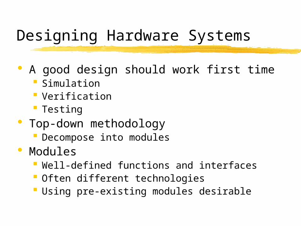
Designing Hardware Systems
A good design should work first time Simulation Verification Testing
Top-down methodology Decompose into modules
Modules Well-defined functions and interfaces Often different technologies Using pre-existing modules desirable
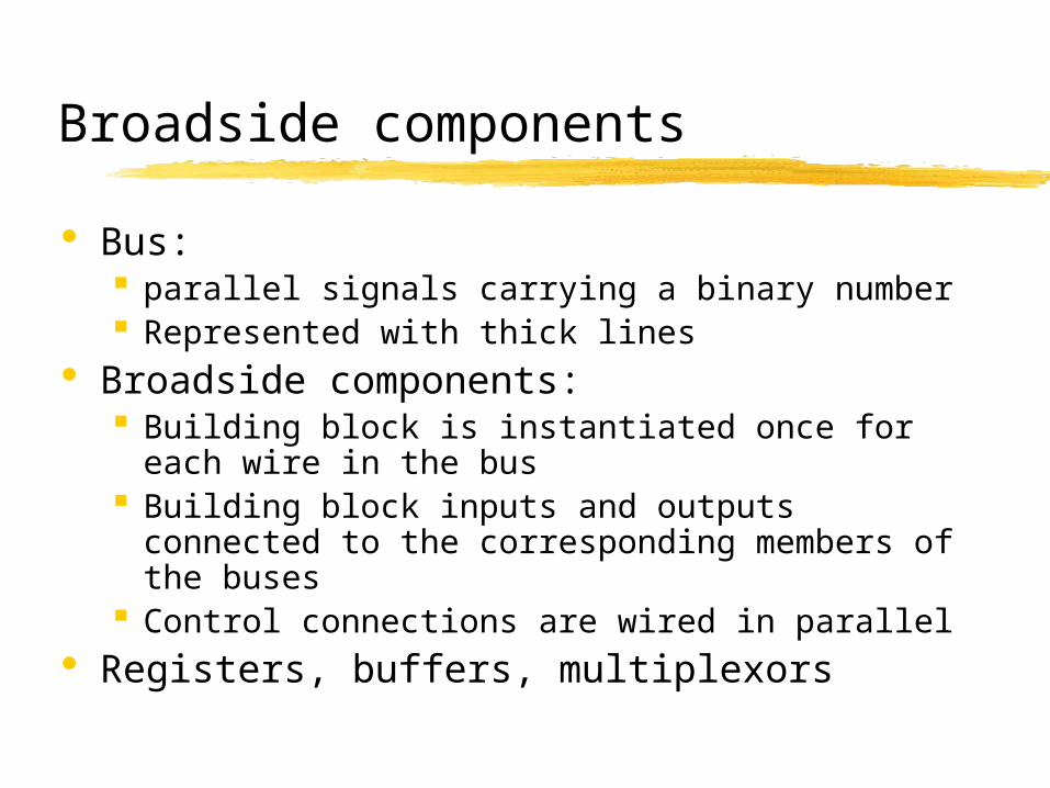
Broadside components
Bus: parallel signals carrying a binary number Represented with thick lines
Broadside components: Building block is instantiated once for each
wire in the bus Building block inputs and outputs connected to
the corresponding members of the buses Control connections are wired in parallel
Registers, buffers, multiplexors

Read-Only Memories
Non-volatile, but typically slow Mask programmable
• Cheapest in mass production by far One-time programmable (PROM) UV Eraseable (EPROM) Electrically re-programmable (e.g. FLASH)
• Expensive, but many rewrite cycles possible• `Field upgrades’ possible
Choose technology based on #units required and #rewrite cycles expected
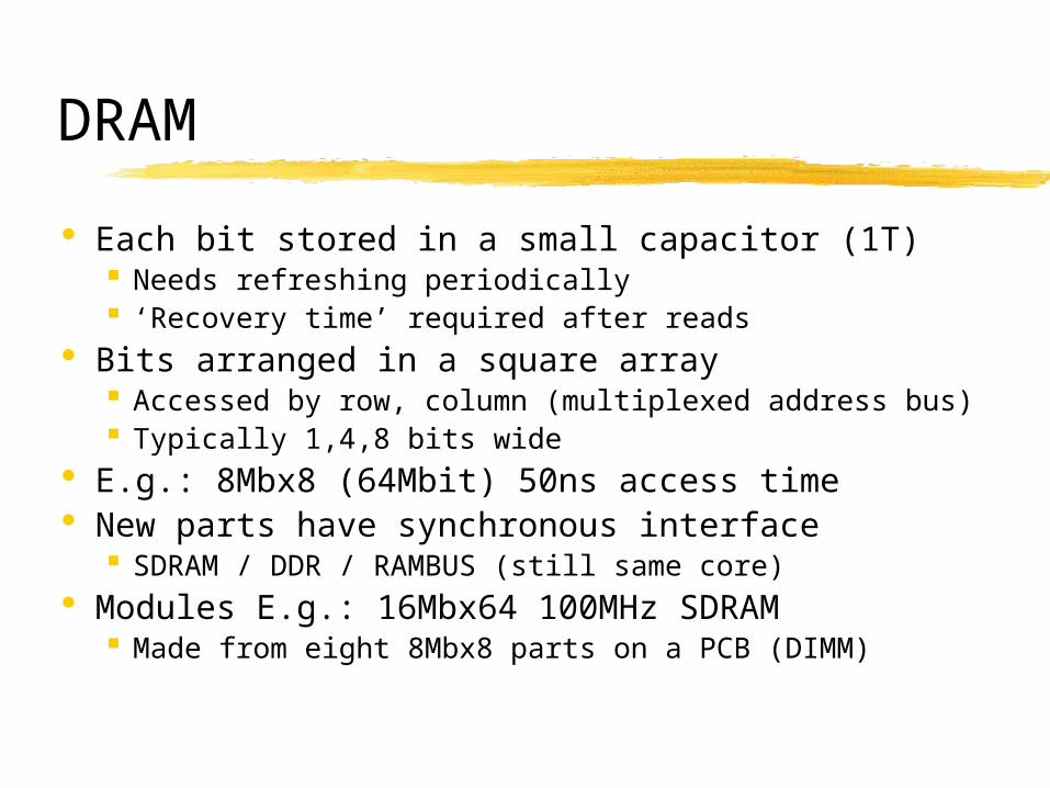
DRAM
Each bit stored in a small capacitor (1T) Needs refreshing periodically ‘Recovery time’ required after reads
Bits arranged in a square array Accessed by row, column (multiplexed address bus) Typically 1,4,8 bits wide
E.g.: 8Mbx8 (64Mbit) 50ns access time New parts have synchronous interface
SDRAM / DDR / RAMBUS (still same core) Modules E.g.: 16Mbx64 100MHz SDRAM
Made from eight 8Mbx8 parts on a PCB (DIMM)
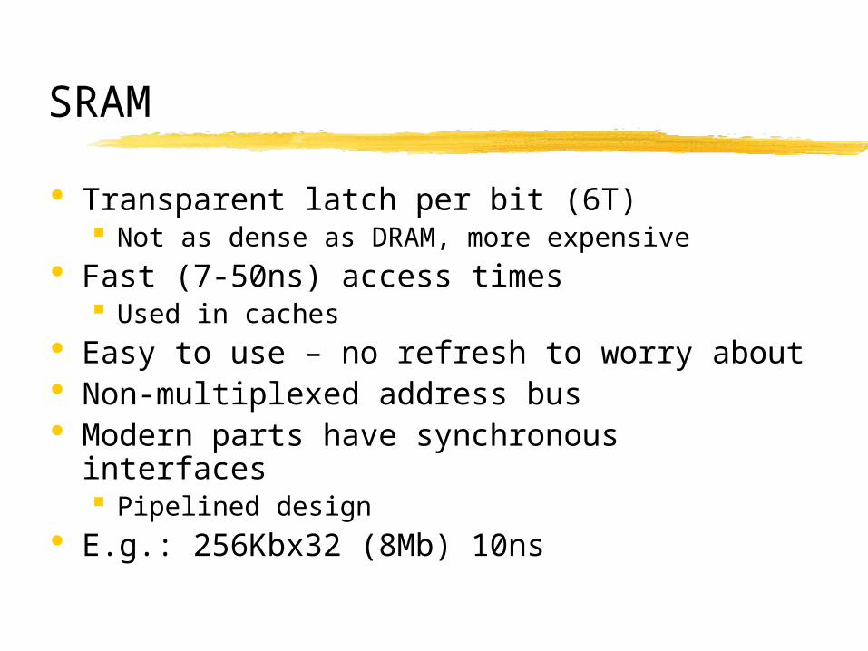
SRAM
Transparent latch per bit (6T) Not as dense as DRAM, more expensive
Fast (7-50ns) access times Used in caches
Easy to use – no refresh to worry about Non-multiplexed address bus Modern parts have synchronous interfaces
Pipelined design E.g.: 256Kbx32 (8Mb) 10ns
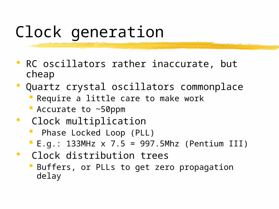
Clock generation
RC oscillators rather inaccurate, but cheap Quartz crystal oscillators commonplace
Require a little care to make work Accurate to ~50ppm
Clock multiplication Phase Locked Loop (PLL) E.g.: 133MHz x 7.5 = 997.5Mhz (Pentium III)
Clock distribution trees Buffers, or PLLs to get zero propagation delay
Miscellaneous
Power-on reset Release reset after power stable Get all flip-flops into known state (manual reset by shorting capacitor)
Relays can be used to switch large loads (alternative is to use power transistors) Must protect transistor with a diode
Mechanical switches ‘bounce’ when switching Use a 2-pole switch and RS latch
ALUs
Combinatorial logic implementation Takes two N-bit inputs and function selector Propagation delay typically determined by
carry chain
Typically twos-complement representation ADD, ADC, SUB, NOT, AND, OR, BIC,… Flags: Carry-out, Negative, Overflow, Zero Output will typically be latched, along with
flag status results
Microprocessors
Simple microprocessor control signals: Inputs: Clock, Reset Output: Request, Read/nWrite, Addr<0..N> InOut: Data<0..M>
Read cycles to fetch instructions and load data
Write cycles when updating memory Begins execution by fetching from reset
location PC incremented unless branch/jump instruction
Address decoding
Devising a memory map for a design Address that memory/peripherals are available
at
Non-volatile memory typically mapped at the reset location
Use combinatorial function of high-order address bits to generate enable signals
Devise memory map for decoding convenience
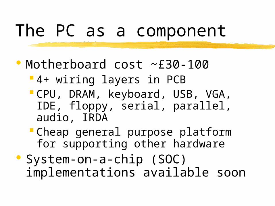
The PC as a component
Motherboard cost ~£30-1004+ wiring layers in PCBCPU, DRAM, keyboard, USB, VGA, IDE,
floppy, serial, parallel, audio, IRDACheap general purpose platform for
supporting other hardware System-on-a-chip (SOC)
implementations available soon
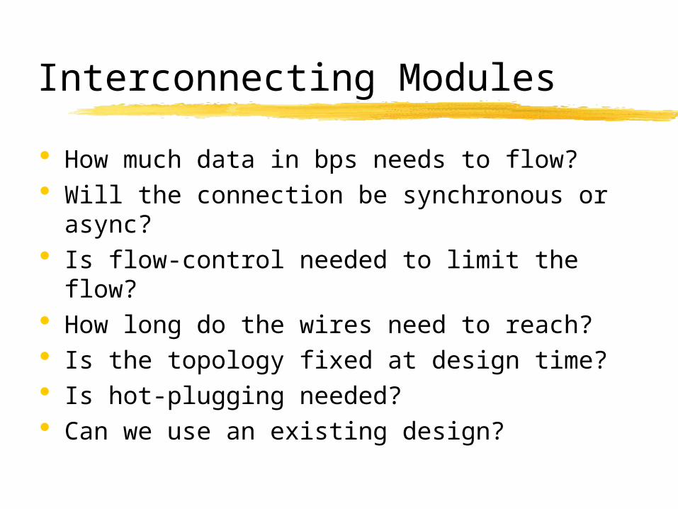
Interconnecting Modules
How much data in bps needs to flow? Will the connection be synchronous or
async? Is flow-control needed to limit the flow? How long do the wires need to reach? Is the topology fixed at design time? Is hot-plugging needed? Can we use an existing design?
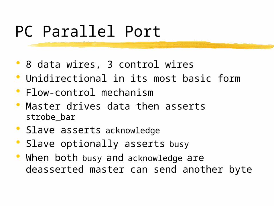
PC Parallel Port
8 data wires, 3 control wires Unidirectional in its most basic form Flow-control mechanism Master drives data then asserts strobe_bar Slave asserts acknowledge Slave optionally asserts busy When both busy and acknowledge are
deasserted master can send another byte
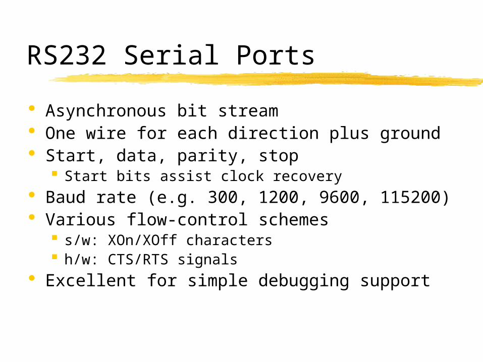
RS232 Serial Ports
Asynchronous bit stream One wire for each direction plus ground Start, data, parity, stop
Start bits assist clock recovery Baud rate (e.g. 300, 1200, 9600, 115200) Various flow-control schemes
s/w: XOn/XOff characters h/w: CTS/RTS signals
Excellent for simple debugging support
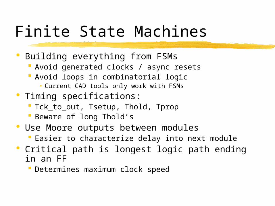
Finite State Machines Building everything from FSMs
Avoid generated clocks / async resets Avoid loops in combinatorial logic
• Current CAD tools only work with FSMs
Timing specifications: Tck_to_out, Tsetup, Thold, Tprop Beware of long Thold’s
Use Moore outputs between modules Easier to characterize delay into next module
Critical path is longest logic path ending in an FF Determines maximum clock speed
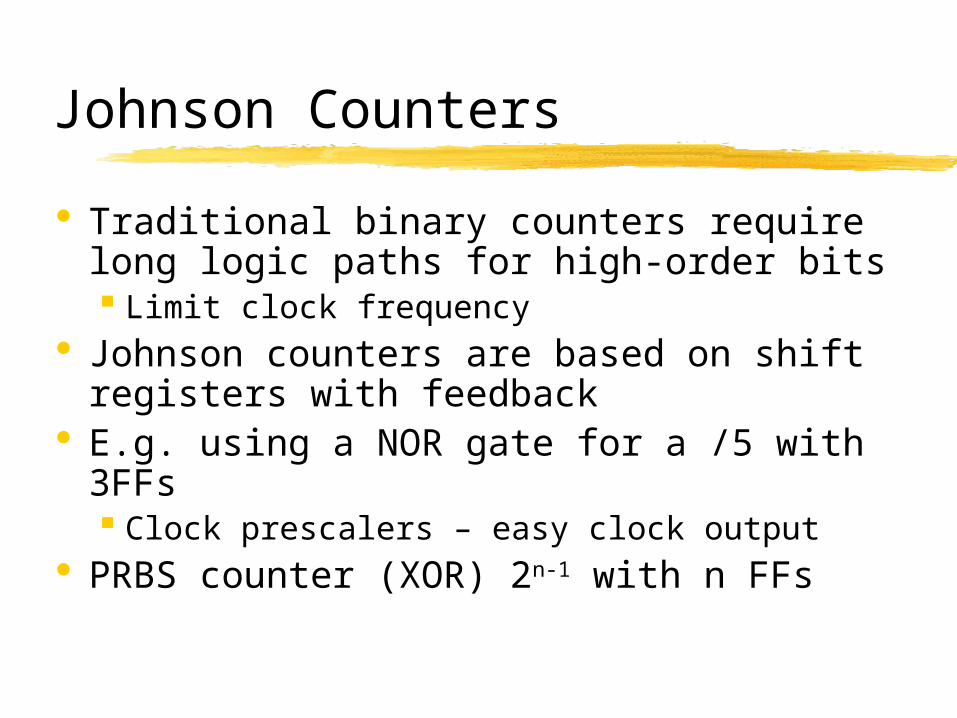
Johnson Counters
Traditional binary counters require long logic paths for high-order bits Limit clock frequency
Johnson counters are based on shift registers with feedback
E.g. using a NOR gate for a /5 with 3FFs Clock prescalers – easy clock output
PRBS counter (XOR) 2n-1 with n FFs
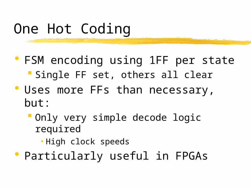
One Hot Coding
FSM encoding using 1FF per state Single FF set, others all clear
Uses more FFs than necessary, but: Only very simple decode logic required
• High clock speeds
Particularly useful in FPGAs
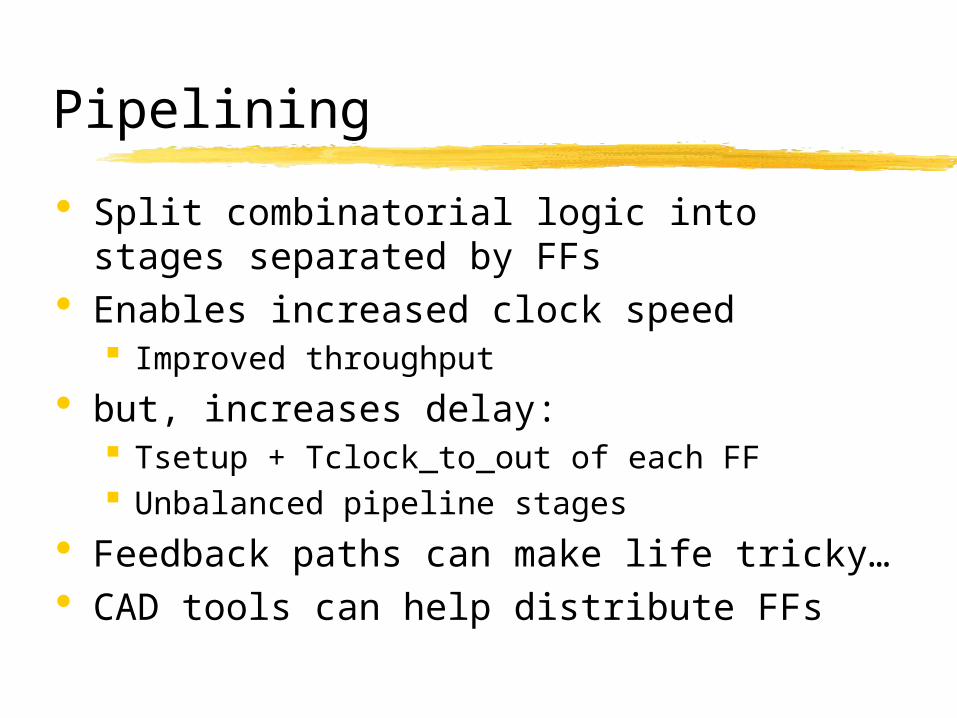
Pipelining
Split combinatorial logic into stages separated by FFs
Enables increased clock speed Improved throughput
but, increases delay: Tsetup + Tclock_to_out of each FF Unbalanced pipeline stages
Feedback paths can make life tricky… CAD tools can help distribute FFs
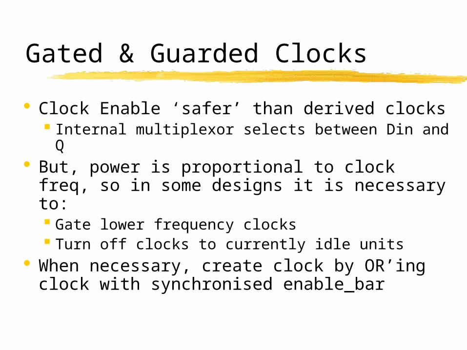
Gated & Guarded Clocks
Clock Enable ‘safer’ than derived clocks Internal multiplexor selects between Din
and Q But, power is proportional to clock freq,
so in some designs it is necessary to: Gate lower frequency clocks Turn off clocks to currently idle units
When necessary, create clock by OR’ing clock with synchronised enable_bar
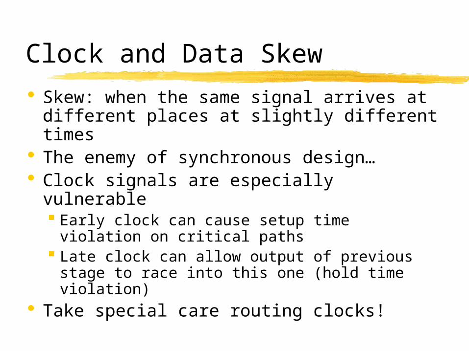
Clock and Data Skew
Skew: when the same signal arrives at different places at slightly different times
The enemy of synchronous design… Clock signals are especially vulnerable
Early clock can cause setup time violation on critical paths
Late clock can allow output of previous stage to race into this one (hold time violation)
Take special care routing clocks!
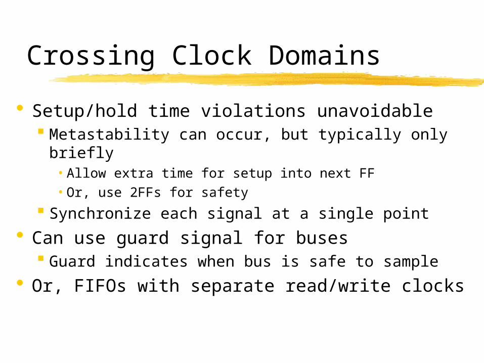
Crossing Clock Domains
Setup/hold time violations unavoidable Metastability can occur, but typically only
briefly • Allow extra time for setup into next FF• Or, use 2FFs for safety
Synchronize each signal at a single point Can use guard signal for buses
Guard indicates when bus is safe to sample Or, FIFOs with separate read/write clocks
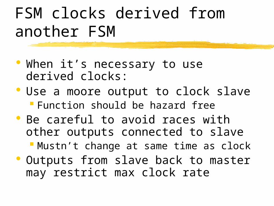
FSM clocks derived from another FSM
When it’s necessary to use derived clocks:
Use a moore output to clock slave Function should be hazard free
Be careful to avoid races with other outputs connected to slave Mustn’t change at same time as clock
Outputs from slave back to master may restrict max clock rate
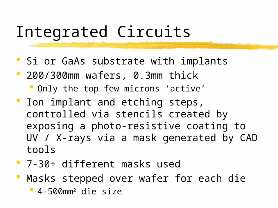
Integrated Circuits
Si or GaAs substrate with implants 200/300mm wafers, 0.3mm thick
Only the top few microns ‘active’
Ion implant and etching steps, controlled via stencils created by exposing a photo-resistive coating to UV / X-rays via a mask generated by CAD tools
7-30+ different masks used Masks stepped over wafer for each die
4-500mm2 die size
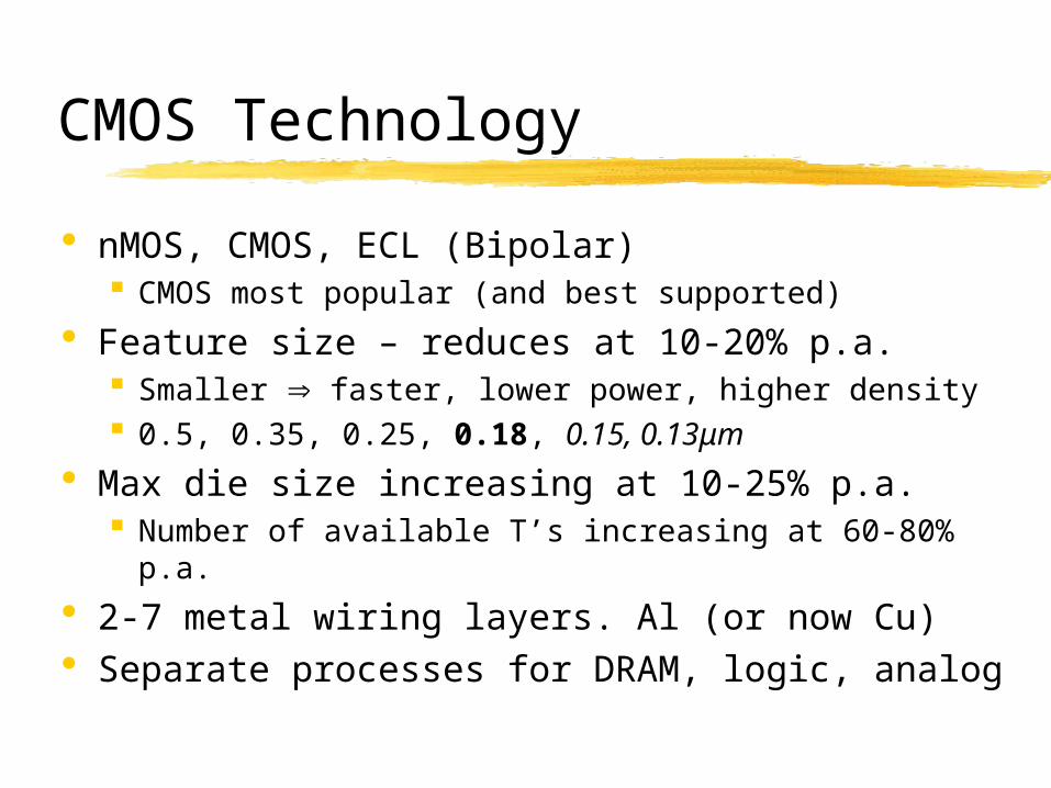
CMOS Technology
nMOS, CMOS, ECL (Bipolar) CMOS most popular (and best supported)
Feature size – reduces at 10-20% p.a. Smaller faster, lower power, higher density 0.5, 0.35, 0.25, 0.18, 0.15, 0.13μm
Max die size increasing at 10-25% p.a. Number of available T’s increasing at 60-80%
p.a.
2-7 metal wiring layers. Al (or now Cu) Separate processes for DRAM, logic, analog

Pads and IO
Pad ring around edge of die Pads are typically 50 micron square Contain high-power drive outputs and ESD
protection circuitry Power / ground ring around pads
Gold bond wires connect to package pins Up to 1000+ pins (with expensive
packaging) Packaging eases handling and dissipates
heat Core bound vs. Pad bound designs

Chip costs
Non Recurring Expenditure (NRE) Design costs (labour, tools, overheads...) Mask making costs
Per device costs Raw wafer, Processing, Testing, Packaging Influenced by yield P(die defect free) Kdie area
• K is probability that any given mm2 is defect free
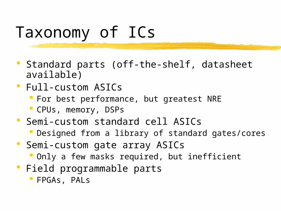
Taxonomy of ICs
Standard parts (off-the-shelf, datasheet available)
Full-custom ASICs For best performance, but greatest NRE CPUs, memory, DSPs
Semi-custom standard cell ASICs Designed from a library of standard gates/cores
Semi-custom gate array ASICs Only a few masks required, but inefficient
Field programmable parts FPGAs, PALs
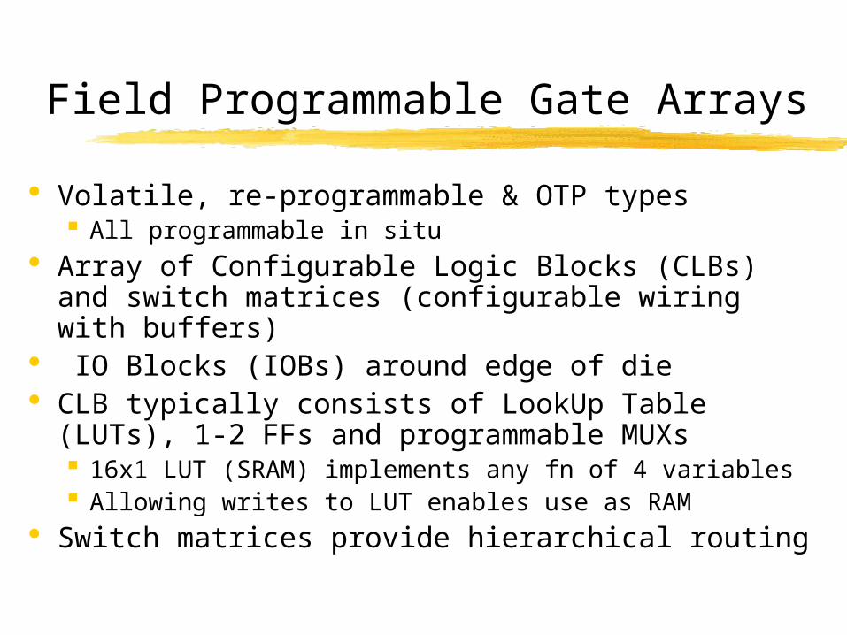
Field Programmable Gate Arrays
Volatile, re-programmable & OTP types All programmable in situ
Array of Configurable Logic Blocks (CLBs) and switch matrices (configurable wiring with buffers)
IO Blocks (IOBs) around edge of die CLB typically consists of LookUp Table (LUTs), 1-2
FFs and programmable MUXs 16x1 LUT (SRAM) implements any fn of 4 variables Allowing writes to LUT enables use as RAM
Switch matrices provide hierarchical routing
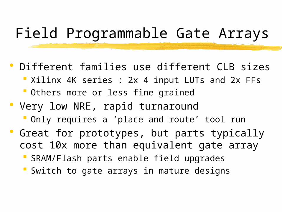
Field Programmable Gate Arrays
Different families use different CLB sizes Xilinx 4K series : 2x 4 input LUTs and 2x FFs Others more or less fine grained
Very low NRE, rapid turnaround Only requires a ‘place and route’ tool run
Great for prototypes, but parts typically cost 10x more than equivalent gate array SRAM/Flash parts enable field upgrades Switch to gate arrays in mature designs

Programmable Array Logic Devices (PALs)
Programmable sum of products array feeding macrocells Good for simple FSMs and glue logic
Macrocell enables combinatorial or registered output, usually tristateable more complex devices also contain buried
macrocells, and may organise macrocells into clusters with separate clock sources, sometimes called CPLDs (Complex Programmable Logic Devices)
New parts in-circuit-programmable, while others require a special programmer JEDEC description file
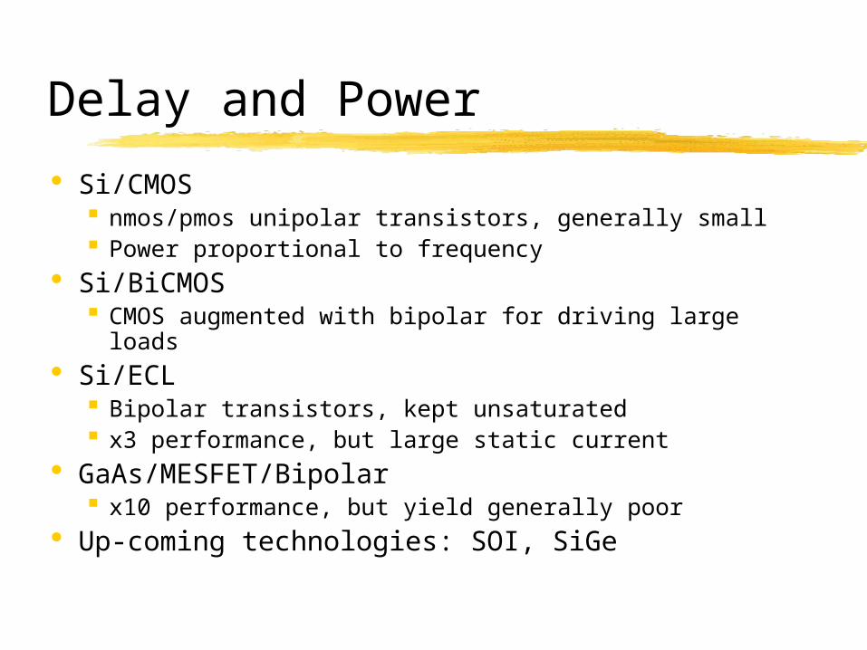
Delay and Power
Si/CMOS nmos/pmos unipolar transistors, generally small Power proportional to frequency
Si/BiCMOS CMOS augmented with bipolar for driving large loads
Si/ECL Bipolar transistors, kept unsaturated x3 performance, but large static current
GaAs/MESFET/Bipolar x10 performance, but yield generally poor
Up-coming technologies: SOI, SiGe
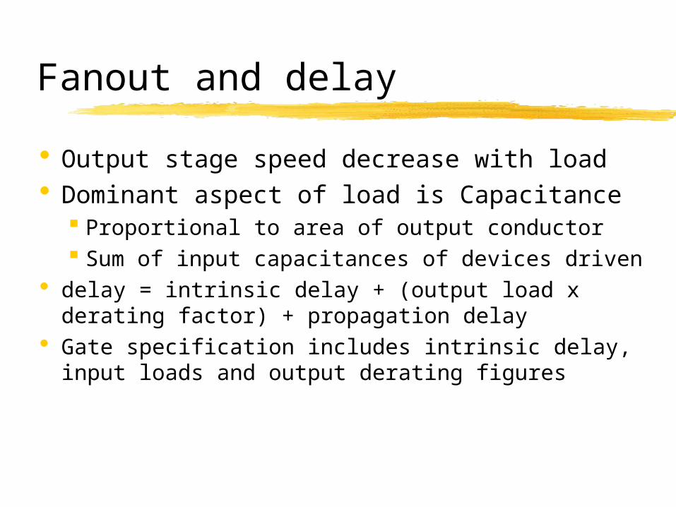
Fanout and delay
Output stage speed decrease with load Dominant aspect of load is Capacitance
Proportional to area of output conductor Sum of input capacitances of devices driven
delay = intrinsic delay + (output load x derating factor) + propagation delay
Gate specification includes intrinsic delay, input loads and output derating figures
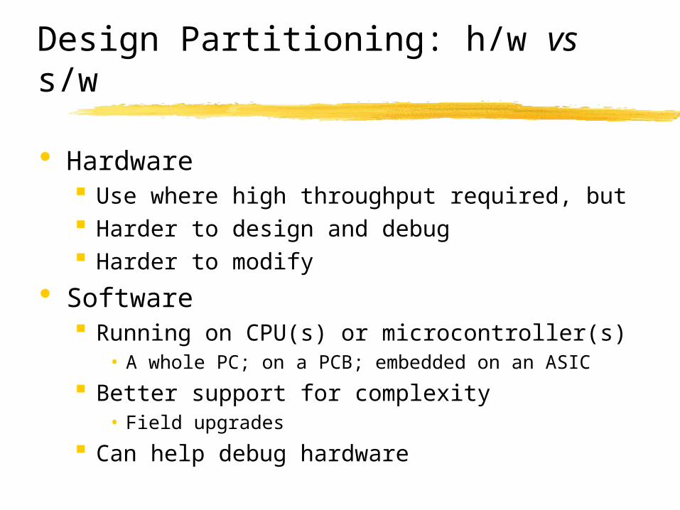
Design Partitioning: h/w vs s/w
Hardware Use where high throughput required, but Harder to design and debug Harder to modify
Software Running on CPU(s) or microcontroller(s)
• A whole PC; on a PCB; embedded on an ASIC
Better support for complexity• Field upgrades
Can help debug hardware
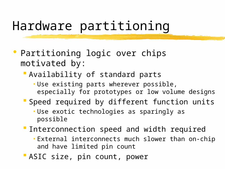
Hardware partitioning
Partitioning logic over chips motivated by: Availability of standard parts
• Use existing parts wherever possible, especially for prototypes or low volume designs
Speed required by different function units• Use exotic technologies as sparingly as possible
Interconnection speed and width required• External interconnects much slower than on-chip
and have limited pin count
ASIC size, pin count, power

Logic Synthesis & Layout
Complex functions expressed algorithmically, then synthesized to gates Good at ‘mechanical’ tasks on relatively small
sections of a design Critical sections of a design still done by hand
Place tool attempts to layout gates to minimize wiring paths
Route tool attempts to wire gates Tools are continually improving
More feed back and integration between tools
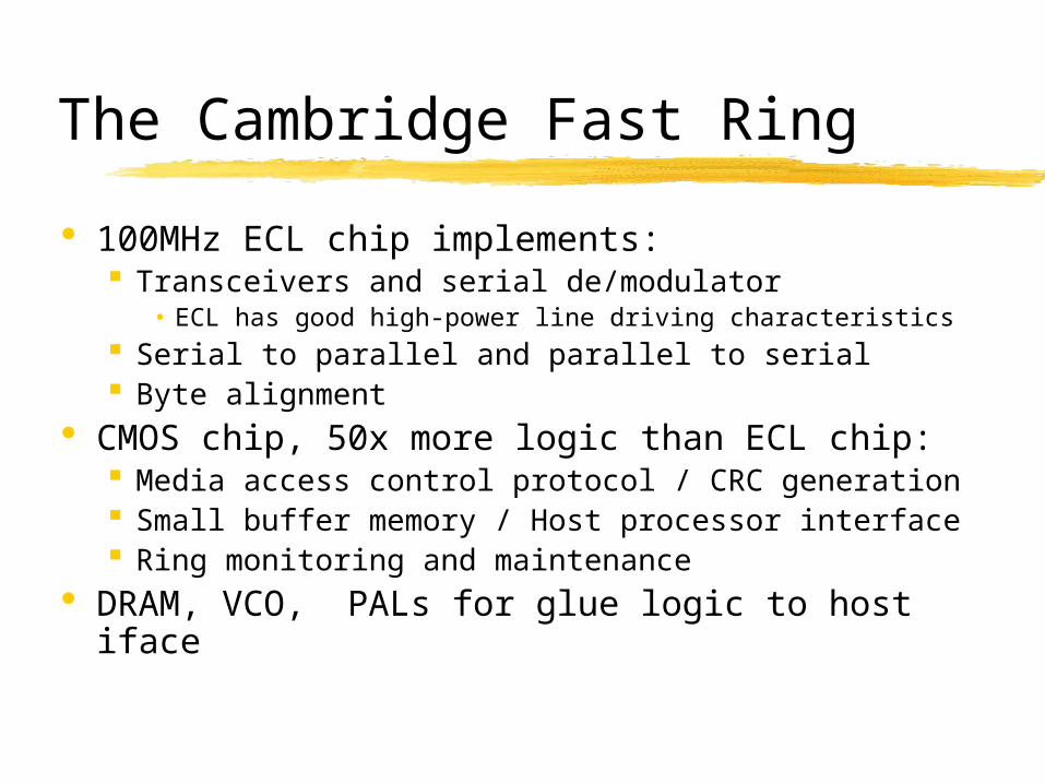
The Cambridge Fast Ring
100MHz ECL chip implements: Transceivers and serial de/modulator
• ECL has good high-power line driving characteristics Serial to parallel and parallel to serial Byte alignment
CMOS chip, 50x more logic than ECL chip: Media access control protocol / CRC generation Small buffer memory / Host processor interface Ring monitoring and maintenance
DRAM, VCO, PALs for glue logic to host iface
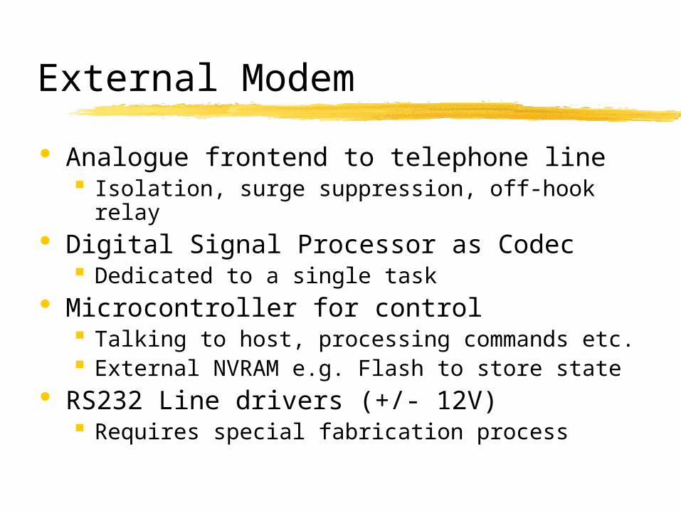
External Modem
Analogue frontend to telephone line Isolation, surge suppression, off-hook relay
Digital Signal Processor as Codec Dedicated to a single task
Microcontroller for control Talking to host, processing commands etc. External NVRAM e.g. Flash to store state
RS232 Line drivers (+/- 12V) Requires special fabrication process
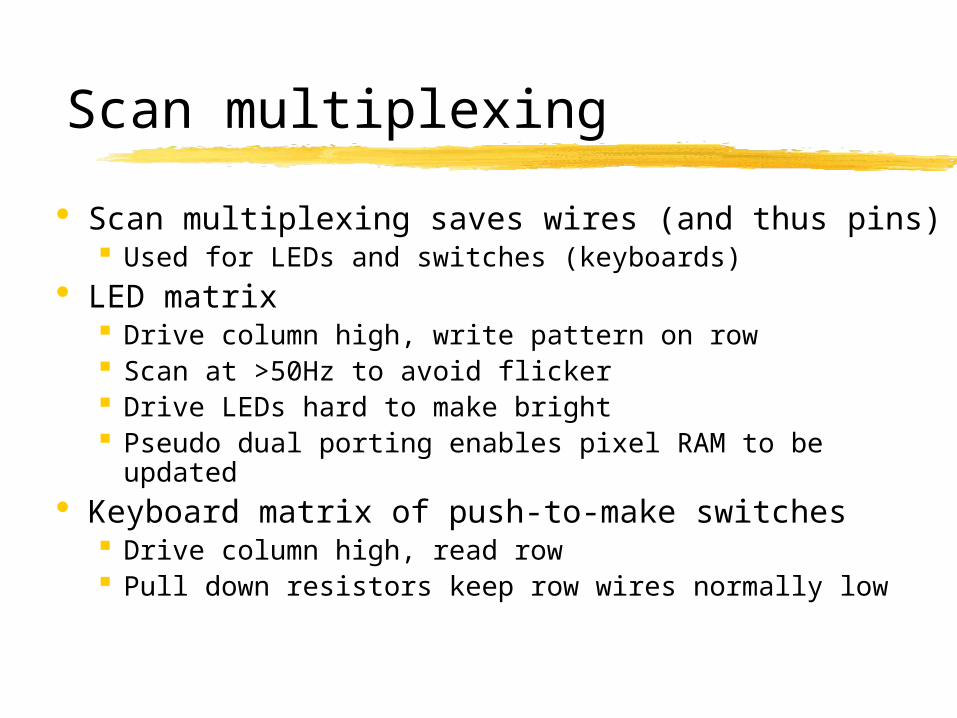
Scan multiplexing
Scan multiplexing saves wires (and thus pins) Used for LEDs and switches (keyboards)
LED matrix Drive column high, write pattern on row Scan at >50Hz to avoid flicker Drive LEDs hard to make bright Pseudo dual porting enables pixel RAM to be updated
Keyboard matrix of push-to-make switches Drive column high, read row Pull down resistors keep row wires normally low
Audio delay unit
Sample clock of 44.1kHz sufficient for audio Single counter provides fixed delay
Read cycle followed by write to same location Two counters (one loadable) and a mux
enables variable delays Lead write counter has over read sets delay Could use LFSR counters, but no need here Could use DRAM, but SRAM easier and dense
enough• Accesses unlikely to be to same page, hence slow
– Could use small staging FIFOs to enable burst reads & writes
Audio so slow, we could use a microcontroller

Network Camera Device :1
Standard parts for: Video frontend and resizer, Audio digitizer JPEG compression engine 100Mb/s Network SERDES (de/serializer)
Three 8KBx8 SRAMs for scanline to tile conversion, controlled by PAL
Three 256KBx8 DRAM FIFOs for framebuffer PAL for colour conversion / muxing (non
compressed)
Network Camera Device :2
FPGA for assembling audio/video/CPU cells for TX 2KBx8 dual ported SRAM acting as small 3 channel FIFO
FPGA for network interface control MAC and CRC generation Determines stream priority and reads cell out of SRAM
and feeds it to SERDES (CoDec)
EPROM microcontroller Communicates over network with management software Co-ordinates frame capture and compression