Embed Size (px)
Citation preview

INORGANIC MATERIALS SCIENCE (IMS)University of Twente
June 22, 2015
Structure and functionalitycorrelation in resistive random
access memory devices
Authors:Thijs van den BergMichiel Hack
Supervisors:Dr. Z. Liao
Prof. dr. ing. A.J.H.M. Rijnders


Abstract
Resistive random access memory (RRAM) is a form of memory. RRAM devicesare able to switch between two resistance states, making it useful for data storage.RRAM devices typically consist of a metal-oxide sandwiched between two metalelectrodes.
In this report the effect of the oxygen pressure during PCMO growth on de-vice performance is researched using Au/Ti/PCMO/SRO/Nb-STO/Ti/Au devices.Using AFM and XRD the influence of oxygen pressure on the structural propertiesof the PCMO was researched. It was found that the crystallinity of the PCMOlayer increases as the oxygen pressure is increased. Devices in which PCMO wasgrown at low oxygen pressure seem to perform better than those in which PCMOwas grown at higher oxygen pressure. The influence of the applied signal onthe stability of the device was also researched. A sweep signal and a signal ofwhich the total voltage sum is zero lead to the best device stability. While theHRS/LRS-ratio of all three devices was sufficient to compete with flash memory,the stability and retention of the devices was not.
The compatibility of PCMO-based RRAM with current CMOS technology wasalso researched. Two devices were grown on silicon substrates. One device(Au/Ti/PCMO/Pt/Ti/SiO2/Si) did not show resistive switching behaviour. Theother device (Au/Ti/PCMO/SRO/STO/Si) does show resistive switching be-haviour. This might be caused by the (110) orientation the PCMO in the Pt/Ti/SiO2
/Si-based device. The orientation of the PCMO in the SRO/STO/Si-based deviceis (002), which is also the orientation used in the devices used for the oxygenpressure measurements. The latter device converges to a HRS/LRS-ratio ofapproximately 3 after 1000 switching cycles. Hence, functioning PCMO-basedRRAM devices can be grown on silicon substrates, meaning that they are compat-ible with current CMOS technology.


Table of Contents
1 Introduction 1
2 Theoretical aspects 32.1 Resistive switching . . . . . . . . . . . . . . . . . . . . . . . . . . . . . 3
2.1.1 Filament and interface type switching . . . . . . . . . . . . . 42.2 PCMO and the role of oxygen vacancies . . . . . . . . . . . . . . . . 6
3 Experimental aspects 83.1 Fabrication techniques . . . . . . . . . . . . . . . . . . . . . . . . . . . 8
3.1.1 Pulsed Laser Deposition . . . . . . . . . . . . . . . . . . . . . . 83.1.2 Radio frequency sputtering . . . . . . . . . . . . . . . . . . . 83.1.3 Lift-off lithography . . . . . . . . . . . . . . . . . . . . . . . . . 10
3.2 Preparation of the devices . . . . . . . . . . . . . . . . . . . . . . . . . 113.3 Characterization of the devices . . . . . . . . . . . . . . . . . . . . . . 13
3.3.1 Atomic Force Microscopy . . . . . . . . . . . . . . . . . . . . . 133.3.2 X-Ray Diffraction . . . . . . . . . . . . . . . . . . . . . . . . . . 143.3.3 Keithley 4200-SCS . . . . . . . . . . . . . . . . . . . . . . . . . 16
4 Results 184.1 Switching type of PCMO-based devices . . . . . . . . . . . . . . . . . 184.2 Influence of oxygen pressure . . . . . . . . . . . . . . . . . . . . . . . 20
4.2.1 Inspection of devices . . . . . . . . . . . . . . . . . . . . . . . 224.2.2 Switching stability of devices 1-3 . . . . . . . . . . . . . . . . 264.2.3 Retention . . . . . . . . . . . . . . . . . . . . . . . . . . . . . . 31
4.3 Devices on silicon substrate . . . . . . . . . . . . . . . . . . . . . . . . 324.3.1 Stability measurements of device 5 . . . . . . . . . . . . . . . 34
5 Conclusion 36
6 Discussion 386.1 Obstacles . . . . . . . . . . . . . . . . . . . . . . . . . . . . . . . . . . . 386.2 Proposed further research . . . . . . . . . . . . . . . . . . . . . . . . . 39
Acknowledgements 40
References 41
A Device information 44


Chapter 1
Introduction
Random access memory (RAM) is an important component of computers, it isused to store (temporary) information. There is an everlasting quest to findmemory devices which are denser, faster and non-volatile. Non-volatile memoryretains information when it is not powered. Current RAM types, such as flashmemory, are reaching their densest possible state. Flash memory cannot becreated at a denser scale, as quantum-mechanical effect would occur.[1]
One proposed and promising memory type is resistive random access memory(RRAM). Ferroelectric RAM[2] and magnetoresistive RAM[3] are other proposedalternatives. RRAM makes use of resistive switching: the device can switchbetween two resistance states. Since RRAM devices have two states, it representsa bit. Each state is assigned a value (‘0’ or ‘1’) to store information.
Several (big) electronics corporations are participating in the race to createthe first commercial RRAM. Examples are Hewlett-Packard, Panasonic, Sonyand Micron.[4][5] Thus far, none of them has succeeded in making RRAM witha memory size that is comparable to current RAM technology. There are stillchallenges to overcome.
Commercially viable RRAM should be compatible with current complementarymetal-oxide-semiconductor (CMOS) technology. CMOS technology is used inmost computer circuitry, and is produced (mainly) on silicon wafers. Hence,RRAM has to function on silicon wafers for it to be compatible with currentCMOS technology. Furthermore, the optimal production conditions of RRAMdevices should be determined. Several aspects, such as layer thickness, deposi-tion temperature[6] and oxygen pressure[7] may be of great influence on RRAMperformance. There are several other important factors, but these (along withsome of the previously noted aspects) will not be discussed in this report.
PCMO is a commonly used metal-oxide in RRAM devices. An advantage ofPCMO-based devices is that their mechanism is interface-type, which leads toscalability advantages.
This report describes research done to determine if PCMO-based RRAM devicesthat are grown on a silicon-substrate are viable. In other words: Is PCMO-based
1

Chapter 1. Introduction
RRAM compatible with current CMOS technology? The compatibility of RRAMwith CMOS technology was researched by growing two silicon-based devices andis discussed in chapter 4.
Furthermore, the influence of oxygen pressure on RRAM device performance wasresearched. The ratio of the two resistance values, switching stability and reten-tion are measures of device performance. Other aspects of device performancewill not be discussed in this report. The influence of oxygen pressure duringPCMO growth is discussed in the first part of chapter 4. Three PCMO-baseddevices were grown at varying oxygen pressures for this research.
The mechanisms involved with resistive switching are explained in chapter 2.The techniques involved in the fabrication of RRAM devices –pulsed laser deposi-tion, sputtering and lift-off lithography– and characterization of RRAM devices–atomic force microscopy, X-ray diffraction and current-voltage sweeps– are de-scribed in chapter 3. Finally chapters 5 and 6 present a conclusion and discussionrespectively.
2

Chapter 2
Theoretical aspects
2.1 Resistive switching
Resistive random access memory (RRAM) is a technique that makes use of thephenomenon of resistive switching. Resistive switching allows a device to switchbetween two (or more) resistance states. Generally a resistive switching deviceconsists of a metal-oxide (MO) sandwiched between two electrodes (the topelectrode, TE, and bottom electrode, BE). Generally the BE is grounded and thevoltage is applied to the TE.
For the purpose of simplicity, consider a device that has two resistance states1:the high resistance state (HRS) and low resistance state (LRS). These two statesare often associated with the binary numbers: ‘0’ and ‘1’. The LRS is defined as‘1’ and the HRS is defined as ‘0’.
There are several operations that can be performed with such a device: theSET operation, the RESET operation and the READ operation. The SET operationsets the device from ‘0’ to ‘1’, the RESET operation does the opposite: it resets thedevice from ‘1’ to ’0’. The READ operation determines in which state the devicecurrently is.
The current-voltage curve of a RRAM device has the shape of a hysteresis, seefigure 2.1 for an example. To determine the resistance, R, a well-known formula–Ohm’s Law– is used:
R=UI
(2.1)
where U is the voltage and I is the current. Combined with the hysteresis–multiple current values for each voltage value– this results in two resistancevalues for each voltage value: the LRS and the HRS.
1There are devices with more than two states.
3

2.1. Resistive switching Chapter 2. Theoretical aspects
Figure 2.1: An example current-voltage curveof a resistive switching device showing the hys-teresis. The arrows indicate the switching po-larity. Figure adapted from [8].
There are two types of switching: unipolar switching and bipolar switching. Inunipolar switching devices, resistive switching occurs at different amplitudes ofthe same polarity. In bipolar switching devices, the polarity and amplitude ofthe signal are both important factors for switching. The current-voltage curvescorresponding to unipolar and bipolar switching are shown in figure 2.2.
Figure 2.2: a) Unipolar switching. b) Bipolarswitching. Figure taken from [9].
2.1.1 Filament and interface type switching
There are two mechanisms for (redox-based) resistive switching: filament typeswitching and interface type switching. These mechanisms model the origin ofthe changing resistive, and are still an active area of research.[10]
In filament type switching devices, a conductive filament is formed in the metal-oxide layer. To create a conductive filament a forming operation is required.During the forming operation oxygen atoms are pulled towards the TE, creating
4

Chapter 2. Theoretical aspects 2.1. Resistive switching
a path of oxygen vacancies – a conductive filament. The device is now in the LRS.To switch the device from the LRS to the HRS, the conductive filament is partiallybroken: oxygen atoms recombine with oxygen vacancies. To switch from LRSand HRS the partially broken conductive filament is restored by again pulling theoxygen atoms from the lattice of the MO to the TE. The forming and switchingprocesses are illustrated in figure 2.3.
Initial state 1. Forming
2. HRS 3. LRSRupture
TE
MO
BE
Figure 2.3: A schematic representation of theforming and switching processes of filamenttype switching. Image adapted from [11].
In interface type switching, the switching takes place at the interface. The metalelectrodes influence the switching behaviour by participating in a redox reactionor in trapping oxygen vacancies.[8]When a filament cannot form, the contactresistances of the interfaces determine the resistance. To obtain resistive switch-ing, one interface should behave Ohmic and the other as a Schottky barrier. Thebarrier height of the Schottky barrier can be adjusted by applying a voltage. Ithas been reported that devices with PCMO as the metal-oxide layer only showresistive switching when combined with a low work function electrode.[12]
The difference between filament type and interface type can be made clearby considering the area dependence of the resistance of the device. If the resis-tance of the device decreases with increasing area, this implies that switchingtakes place over the entire area: interface type. If the resistance of the deviceis independent of the area, this implies that switching is a local phenomenon:filament type. In some cases of interface type switching a forming operation isrequired to induce resistive switching, this can be understood as an oxidationprocess (and not as the creation of a filament as is the case for filament typeswitching).
5

2.2. PCMO and the role of oxygen vacancies Chapter 2. Theoretical aspects
2.2 PCMO and the role of oxygen vacancies
PCMO (Pr1-xCaxMnO32) is a material that shows resistive switching behaviour of
interface type when sandwiched between two electrodes.[13][14]
In devices with a titanium TE a thin metal-oxide layer (TiO2) is formed be-tween the PCMO and the TE. To date, PCMO devices have shown only bipolarswitching, suggesting that this metal-oxide layer has a critical role in the resistiveswitching of PCMO-based devices. The resistance of the oxide layer in the LRS issmall, but in the HRS the resistance of the oxide layer is large and dominates thedevice.
A possible explanation is as follows: oxygen vacancies transform the TiO2 layerfrom an insulator into a semiconductor. When a positive voltage is applied to theTE, the oxygen vacancies (positively charged) are driven out of the TiO2 to thePCMO layer, changing the TiO2 layer from a semiconductor to an insulator. Asa result the device switches from the LRS to the HRS. When a negative voltageis applied, the oxygen vacancies are attracted to the TiO2 layer and the deviceswitches from the HRS to the LRS.[13] This is illustrated in figure 2.4.
This mechanism also explains the direction of switching seen in figure 2.1. Thedevice starts with the oxygen vacancies in the PCMO layer (LRS, line with highestcurrent). After applying a potential the oxygen vacancies are moved to the TiO2
layer (HRS, line with lowest current). By applying a negative voltage, the reverseoccurs, and the device switches from the HRS to the LRS (in the negative voltageregion: line with lowest absolute current to line with highest absolute current).
= oxygen vacancy
Metal oxide
ElectrodeLRS HRS
+-+-
Figure 2.4: A schematic representation of inter-face type switching. Top row: the two differentresistance states. Bottom row: the switchingprocesses.
2In this research Pr0.7Ca0.3MnO3 was used.
6

Chapter 2. Theoretical aspects 2.2. PCMO and the role of oxygen vacancies
More recently, Herpers researched a PCMO-based device with a Ti electrode,and found that the resistive switching behaviour is caused by a reversible redox-reaction at the PCMO/Ti interface. The redox-reaction causes an insulatingtunnel barrier to grown and shrink, which in turn causes the resistance of thedevice to increase or decrease.[15]
7

Chapter 3
Experimental aspects
3.1 Fabrication techniques
Before any measurements could take place, the devices had to be fabricated.Mainly sputtering, pulsed laser deposition and lithography were used for thefabrication of the devices. These techniques will be discussed in this section, aswell as the exact process of fabricating a device.
3.1.1 Pulsed Laser Deposition
Pulsed laser deposition (PLD) is a technique used to deposit thin films. As itsname suggests, it makes use of laser pulses. These pulses are sent to the targetthat is desired to be deposited, where the energy of the pulses will be absorbed.The absorbed energy releases the atoms on the surface of the target. The atomswill evaporate and ionize due to the high energies, and a plasma will form. Theplume of this plasma, consisting of several particles such as energetic neutralatoms, ions, electrons and atom clusters, is highly directional. The content of theplume can therefore be propelled towards the substrate, where it will condensateand form a film. The substrate is heated to create more crystalline layers. Athigher temperatures atoms can move more easily to a ‘hole’ in the substrate,therefore flatter layers are obtained when the substrate is heated.
The PLD process is operated in ultra high vacuum to reduce contaminationsof the growing film. However some gases such as O2 and N2 are often releasedinto the deposition chamber to promote surface reactions or maintaining filmstoichiometry.[16]
Figure 3.1 shows a schematic view of an example of a PLD system.
3.1.2 Radio frequency sputtering
Sputtering is another often used thin layer deposition technique. Atoms that ejectfrom source surfaces due to impact of gaseous ions form the main mechanismfor sputtering. There are several sputtering techniques, radio frequency (RF)sputtering and RF magnetron sputtering will be discussed here.
8

Chapter 3. Experimental aspects 3.1. Fabrication techniques
Figure 3.1: Schematic view of a PLD system.Figure taken from [17]. An UV excimer beamshines (pulsed) on the target material to createa plasma plume. The CO2 is used to heat thesubstrate. The DC stepper motor moves thetarget continuously to make sure that the UVexcimer beam shines on all parts of the targetto prevent the forming of holes.
Figure 3.2: Schematic view of a RF sputteringsystem. Figure taken from [18].
RF sputtering is schematically shown in figure 3.2. A radio frequency signal ofusually 13.56 MHz is applied to the anode and cathode. The substrates are placedon the anode and the target is the cathode. Since electrons have a much highermobility than the ions of the sputter gas, the electrons will form layers at both ofthe electrodes. The negative potential, caused by the electrons, will thereforeattract the ions to both of the electrodes and sputter at both the substrate andtarget. Since the size of the target is much smaller than the size the of the anode,the voltage drop at the target is much greater than at the anode. Therefore the
9

3.1. Fabrication techniques Chapter 3. Experimental aspects
ions will be attracted more to the target and mainly atoms of the target will besputtered. Those sputtered atoms will drop down and form a thin film on thesubstrate.
In this research a variation of RF sputtering called RF magnetron sputteringwas used. In RF magnetron sputtering, magnets are added to the depositionchamber. Several magnet configurations are possible, but they all rely of thesame principle. The magnetic field traps electrons and/or ions close to the sub-strate. This increases the probability of collisions between electrons, ions andatoms. In turn, this results in a denser plasma near the target. A denser plasmacauses higher sputtering rates and thus higher deposition rates. Consequently,RF magnetron sputtering is faster than ordinary RF sputtering.[19]
(e)
(d)
(c)
(b)
(a)
Figure 3.3: Schematic overview of the lift-offprocess. (a) UV light passes through a reticle.(b) Some parts of the photoresist are exposedto the light (orange colour), other parts arenot (red colour). (c) The non-exposed areasare removed. (d) A metal is deposited ontothe sample. (e) Using lift-off, the exposed pho-toresist is removed along with unwanted metaldepositions.
3.1.3 Lift-off lithography
The previously described techniques, PLD and (RF-)sputtering, can only growflat thin films. However, for many experiments devices with diverse structuresare needed. These structures can be created by using of lithography. There are
10

Chapter 3. Experimental aspects 3.2. Preparation of the devices
several lithography techniques, only lift-off lithography will be discussed here.Lift-off lithography is mainly based on the properties of the photoresist. This isa substance that can be dissolved in certain solutions after1 it is lighted by UV light.
Figure 3.3 shows the process of lift-off lithography. First, the sample is spin-coated with photoresist. UV light is then beamed at the sample through a reticle(mask) that contains the desired pattern. In figure 3.3 a negative photoresistis used. After placing the sample in development solvent, only the enlightenedparts of the photoresist are left on the sample. Next, the desired layer(s) ofmaterials are deposited on the sample by (for example) sputtering or PLD. Lastly,the sample is placed in ethanol and acetone to let the photoresist dissolve. Thematerials deposited directly on top of the photoresist will also be removed fromthe sample due to the dissolving photoresist underneath. The sample now hasthe same structure as the reticle.2
3.2 Preparation of the devices
To produce the RRAM devices used for this research, all of the fabrication tech-niques described in section 3.1 were used. The properties of all devices are shownin appendix A.
Devices 1-3 are similar in every aspect except the oxygen pressure during PCMOgrowth. The composition of devices 1-3 is shown in figure 3.4. The choice forthis composition was based on previous research by others, which shows thata device with this composition is able to resistively switch between states.[8]Buffer layers are used to match the lattice parameters of mismatching layers.
The substrate of the device is a niobium (Nb) doped strontium titanate (SrTiO3,commonly abbreviated as STO) layer. On this substrate, a 60nm thick layer ofSrRuO3 was grown using PLD. Next, a 100nm thick PCMO layer was grown usingPLD. The oxygen pressure during the growth of the PCMO layer was different fordevices 1-3. Device 1 was grown at an oxygen pressure of 0.2mBar, device 2 wasgrown at an oxygen pressure of 0.2mBar for 20nm then at 10-3mBar for 80nm,device 3 was grown at an oxygen pressure of 5×10⁻⁵mBar.
Next, photoresist was spincoated on the devices and using the method de-scribed earlier, the pattern of the electrodes was applied to the device. Threedifferently sized electrodes were applied: 50µm×50µm, 100µm×100µm and200µm×200µm. Of each size, multiple electrodes were applied to the samedevice. The electrodes consist of 100nm gold (Au) on top of 16nm(top elec-trode)/18nm(bottom electode) titanium (Ti). Sputtering was used for the appli-cation of the electrodes. Lift-off lithography was used to remove unwanted Auand Ti.
1Or before, this depends on whether it is a ‘positive’ or ‘negative’ resist.2This is true only when a negative photoresist is used. When a positive photoresist is used,
the device structure will be the negative of the reticle.
11

3.2. Preparation of the devices Chapter 3. Experimental aspects
AuTi
AuTi
PCMO
SRONb-STO
V/I
Figure 3.4: Schematic view of the layers ofdevices 1 - 3. Thicknesses are not to scale.Also shown is the application of the potential.
Finally, the device was glued to a metal plate using conducting glue. This makesattaching probes to the device easier. The device is now ready for measurement.
For devices 4 and 5 a similar process was used, although the composition of thedevices is different. The structure of device 4 is: Au/Ti/PCMO/Pt/Ti/SiO2/Si,PCMO was grown at an oxygen pressure of 10-3mBar. The structure of device5 is: Au/Ti/PCMO/SRO/STO/Si, PCMO was grown at an oxygen pressure of5×10-5mBar. The composition of devices 4 and 5 is shown in figure 3.5.
Devices 4 and 5 were produced on silicon to show that RRAM is compatiblewith current CMOS technology, which is produced (almost exclusively) on siliconwafers. CMOS technology is used in microprocessors, microcontrollers, logiccircuits and other circuits.
V/I
AuTi
PCMO
PtSi
(a)
V/I
Si
AuTi
PCMO
SROSTO
(b)
Figure 3.5: Schematic views of the layers of:(a) device 4, (b) device 5. Thicknesses are notto scale.
12

Chapter 3. Experimental aspects 3.3. Characterization of the devices
Figure 3.6a shows a photograph of the device glued to the metal plate. Figure3.6b shows a microscopic image of the device. The differently sized electrodescan clearly be seen.
(a) (b)
Figure 3.6: Images of the device. (a) Imageshowing the device glued to the metal plate.(b) Microscopic image of the device.
3.3 Characterization of the devices
To determine the performance of the devices, they have to be characterized. Thedevices are characterized in two ways: electrical characterization and structuralcharacterization. Electrical characterization is concerned with the performanceof the resistive switching behaviour, it is focused on the output of the device.The structural characterization is concerned with the structure of the device, thisincludes the crystallinity and morphology of the device.
To characterise the devices, several techniques are used, such as atomic forcemicroscopy and X-ray diffraction. The techniques used for the characterizationof the devices are described in this section.
3.3.1 Atomic Force Microscopy
Atomic force microscopy (AFM) is a technique that is widely used in various fieldsto image surfaces. The resolution of this technique can reach values smaller than1nm (in the z-direction). AFM uses a tip attached to a cantilever. When the tipapproaches the surface of the sample it gets attracted or repulsed by the surface.The attraction or repulsion is caused by the inter-atomic potential between thetip and surface, which only occurs for short distances between the tip and surface.
When a surface is scanned, the tip moves across the surface and moves up anddown due to height differences in the surface. The deflection of the cantilever is ameasure of the height of the surface. The deflection of the cantilever is measuredby a laser beamed at the cantilever. The beam deflects from the cantilever into a
13

3.3. Characterization of the devices Chapter 3. Experimental aspects
detector. Since the cantilever can be considered a spring, the force on the tip canbe determined by Hooke’s law:
F = −kx (3.1)
A schematic view of an AFM is shown in figure 3.7. A feedback loop regulatesthe height of the sample such that the interaction force between tip and sampleremains constant.[20]
Figure 3.7: Schematic view of an AFM. Figuretaken from [20].
There are several measurement modes used in AFM imaging. In this research, the‘tapping’ mode was used for imaging. In tapping mode the cantilever oscillatesnear its resonance frequency and the oscillation amplitude is 20-200 nm. The tipmakes contact with the surface of the sample for a very short period of time ineach oscillation. During this period of time, the tip-sample interaction changesthe amplitude, resonance frequency and phase angle of the oscillating lever. Theamplitude of the cantilever is chosen such that the probe has enough energy topass back and forth through contamination on top of the sample.[20]
3.3.2 X-Ray Diffraction
X-ray diffraction (XRD) is a technique that is widely used to identify the atomicstructure of samples. The technique is based on diffraction. When two incidentalwaves interfere (are in phase), a diffraction pattern appears. The condition forsuch an interference is given by Bragg’s law:
nλ= 2d sin θ (3.2)
Where θ is the angle of incidence, λ the wavelength of the incidental light, d isthe distance between two planes (of atoms) and n is an integer. Bragg’s law isillustrated in figure 3.8.XRD is based on this principle. Light with a very low wavelength (X-rays) is sentinto the sample. The intensity of the diffracted beam is measured. An XRD setupis shown schematically in figure 3.9a.
A monochromatic beam of X-rays is incident at an angle Ω with the sample.
14

Chapter 3. Experimental aspects 3.3. Characterization of the devices
Figure 3.8: Schematic view of Bragg’s law. Fig-ure taken from [21].
The beam is diffracted by the sample (the crystal in figure 3.9) and is detected byan X-ray detector. The angle between the incident X-ray beam and the detectoris defined as 2θ . In figure 3.9b the rotational axes with respect to the sampleholder are shown. The detector and source can be rotated around these axes, theangles Ω and 2θ can also be varied. Measuring the intensity of the varied anglesprovides information about the sample. In this report only 2θ −Ω and Ω scansare discussed.
Figure 3.9: Schematic view of a XRD setup.Figure taken from [22].
2θ −Ω scanDuring a 2θ −Ω scan both the detector and source are rotated in the ω direction.In this mode symmetrical reflexes (Ω = θ) are used. To maintain this property thedetector and source move at the same angular velocity, but in opposite direction.
This technique is often used to determine the unit cell of the sample. Thecomposition and strain of the layers in the sample can also be determined usingthis technique.[23]
Ω scanIn an Ω scan, in which a rocking curve is measured, the detector and source arerotated in the ω–direction as well. This time, however, they move in the samedirection with exactly the same angular velocity. The angle between the detector
15

3.3. Characterization of the devices Chapter 3. Experimental aspects
and source therefore remains constant, but the angle between the sample anddetector/source is varied.
From the rocking curve (intensity as a function ofω) the full width half maximum(FWHM) is often determined and used as a measure for the grain size of a sample.For powder this size can be calculated exactly, but for thin film layers this isnot possible. The FWHM can however be used to compare the grains of twosamples.3[22]
3.3.3 Keithley 4200-SCS
The Keithley 4200-SCS was used to measure current-voltage sweeps and thestability of the devices. The Keithley allows the user to input a custom volt-age array that will be applied to the sample. Simultaneously, the Keithley willmeasure the current. This means that every desired voltage signal can be cre-ated and applied to the sample and the current can be measured at the same time.
The voltage lists used in this report were generated in MATLAB. Two signaltypes were used, these are described below.
Current-voltage sweepThe current-voltage sweep is a measurement in which the voltage is varied asfollows: 0→ VMAX → 0→ –VMAX → 0, with linear steps between the mentionedvoltages.
Current-voltage sweeps were frequently used to check whether the current-voltagecurve of a device shows a hysteresis (and therefore shows resistive switchingbehaviour), before doing longer measurements.
Current-voltage sweeps were also used to determine the stability of the devices.A signal of 200 sweeps was applied to the devices and the current was measuredby the Keithley. The decay of the device can be determined by calculating theHRS/LRS-ratio at a certain voltage (VREAD) for each sweep. These measurementswere performed on all devices for all electrode sizes.
PulsesAnother signal that was used consists of pulses. The device is first SET by alarge positive voltage, then READ by a lower voltage (can be either positiveor negative), then RESET by a large negative voltage and finally READ oncemore (by the same voltage as the previous read signal). Thus: VSET → VREAD
→ VRESET → VREAD. The values of VSET, VRESET and VREAD were varied with eachmeasurement series.
A signal like this was used for the determination of the switching type of thedevices (interface type or filament type). A signal consisting of 20 pulses was
3In figure 3.9 and in this text other symbols are used for the angles than the XRD in the Mesa+NanoLab (PANalytical X’Pert3 Powder). The XRD uses ω instead of Ω. However, the definition ofθ is the same.
16

Chapter 3. Experimental aspects 3.3. Characterization of the devices
applied to all electrode sizes. The mean value of the HRS and LRS (as determinedby the first and second VREAD of each pulse) was determined, and compared tothat of other electrode sizes.
The stability of the devices was also determined by applying pulse signals. Asignal of 1000 pulses was applied to the devices, again to all electrode sizes.The values of the HRS and LRS were determined and divided to obtain theHRS/LRS-ratio. The progression of the HRS/LRS-ratio over time or pulse givesan indication of the stability of the device.
A similar measurement as the one described above was also performed. Inthis case, the signal is slightly different: VSET → VREAD → –VREAD → VRESET →VREAD → –VREAD. The sum of all the voltages in this signal is zero. This couldresult in less charge accumulation at the interfaces in the device, as the oxygenvacancies in the PCMO are attracted to both sides at the same rate. This couldresult in a better stability of the device. Processing the results is done similarlyto that of the signal described above.
A retention measurement was also performed using the Keithley. Since RRAMdevices are non-volatile it should conserve its data without power. Hence: theresistance of the device should remain constant over time without applying asignal. To determined the retention, the device is first SET, after which the deviceis immediately READ. No signal was applied for a period of 90 minutes, afterwhich the device was READ again. The retention of the HRS can be determinedthis way. The retention of the LRS was also determined in the same way, butinstead of applying a SET signal, a RESET signal was applied.
17
Chapter 4
Results
4.1 Switching type of PCMO-based devices
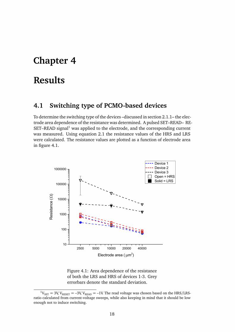
To determine the switching type of the devices –discussed in section 2.1.1– the elec-trode area dependence of the resistance was determined. A pulsed SET–READ– RE-SET–READ signal1 was applied to the electrode, and the corresponding currentwas measured. Using equation 2.1 the resistance values of the HRS and LRSwere calculated. The resistance values are plotted as a function of electrode areain figure 4.1.
5000 200002500 10000 4000010
100
1000
10000
100000
1000000
Device 1 Device 2 Device 3 Open = HRS Solid = LRS
Res
ista
nce
()
Electrode area ( m2)
Figure 4.1: Area dependence of the resistanceof both the LRS and HRS of devices 1-3. Greyerrorbars denote the standard deviation.
1VSET = 3V, VRESET = –3V, VREAD = –1V. The read voltage was chosen based on the HRS/LRS-ratio calculated from current-voltage sweeps, while also keeping in mind that it should be lowenough not to induce switching.
18

Chapter 4. Results 4.1. Switching type of PCMO-based devices
A linear dependence between the electrode area and resistance values can be seenin figure 4.1. This dependence is a characteristic of interface type switching.[9]It implies that the switching takes placed over the entire area of the electrode.
There are two points that deviate from the linear: the LRS 50µm electrodefor both device 1 and device 3 is lower than predicted by the linear dependence.No clear reason was found for this deviation.
It can be concluded that the switching in devices 1-3 is of interface type. Thisconfirms earlier results by others.[13][14]
The switching type of device 5, a device grown on a SRO/STO/Si-stack, was alsodetermined using the same measurement method. The resulting area dependenceof the resistance is shown in figure 4.2.
5000 200002500 10000 4000010
100
1000
10000
100000
1000000
Res
ista
nce
()
Electrode area ( m2)
Open = HRS Solid = LRS
Figure 4.2: Area dependence of the resistanceof both the LRS and HRS of device 5.
The resistance is not dependent on the electrode area: it remains constant re-gardless of the electrode area. It looks as though this device shows filament typeswitching, but this seems unlikely. The device structure is nearly the same as thestructure of devices 1-3, meaning that one would expect interface type switchingto be the mechanism for this device as well.
It is possible that an error was made during the measurement, causing theresistance of another layer to be dominant over the TiO2 layer’s resistance, lead-ing to a stable resistance value.
19

4.2. Influence of oxygen pressure Chapter 4. Results
Another possibility is that this was caused by the lift-off process of device 5.The surface of device 5 shows irregularities not observed in any other device. Itis suspected that either part of the PCMO layer was removed during the lift-offprocess or that there is some acetone left on the surface of the device. Either casemay have influenced the results.
Both cases, however, do not give an explanation for the fact that there aretwo different resistance states, which indicated that resistive switching does takeplace and is measurable. More research on this device is needed to find the exactcause of this unlikely result.
4.2 Influence of oxygen pressure
The importance of oxygen in PCMO for resistive switching became apparantwhen measuring device 2356.2 Prior to annealing3 the device with oxygen, thedevice showed almost no resistive switching: the hysteresis was very small. Afterannealing the device in air for one hour4, the device showed much better resistiveswitching characteristics. The size of the hysteresis increased, and the HRS/LRS-ratio also increased. Prior to annealing the highest HRS/LRS-ratio achievedwas approximately 1.7, after annealing the highest HRS/LRS-ratio achieved wasapproximately 15. A significant increase. The current-voltage sweeps are shownin figure 4.3.
2Device 2356 was not produced in-house, details of the device are unknown. The compositionis: Pt/Ti/PCMO/SRO/CeO2/YSZ/Si.
3Annealing is a process in which the device is heated to above its recrystallization temperature,allowing it to undergo significant changes.
4T = 500C
20

Chapter 4. Results 4.2. Influence of oxygen pressure
-6 -4 -2 0 2 4 6
-0.002
-0.001
0.000
0.001
0.002
0.003
Cur
rent
(A)
Voltage (V)
Prior to O2-annealing After O2-annealing
Figure 4.3: Current-voltage sweeps of device2356 prior to and after annealing with oxy-gen. The performance of the device increasedgreatly after O2-annealing. The arrows indi-cate the switching polarity, which is the samefor both measurements.
This result is consistent with earlier research by Kim, which states: “The resis-tance ratio of HRS and LRS was increased by oxygen annealing of the PCMO thinfilm.”.[24] There is, however, more recent research which found that hysteresissize does not keep increasing with increasing oxygen pressure, in other words:there is a maximum.[25]
More important than the size of the hysteresis is the obtained HRS/LRS-ratio. Alarge hysteresis could have a smaller HRS/LRS-ratio than a smaller hysteresis.In that case, the device with the bigger HRS/LRS-ratio (and smaller hysteresis)is better suited for resistive switching applications. Waser notes that HRS/LRS-ratios > 10 are required to compete with flash memory.[9] Other aspects, suchas stability, are also very important.
While this is not a measurement that proves that resistive switching is dependenton oxygen pressure in one way or another –to do that more information aboutthe device would be needed– it does show that there is reason to research theinfluence of oxygen pressure on the functioning of resistive switching devices.
The current-voltage sweeps corresponding to devices 1-3 are shown in figure4.4. The inset of figure 4.4 shows the absolute value of the current plottedlogarithmically. This gives a clearer image of the positive side of the hysteresis.
21

4.2. Influence of oxygen pressure Chapter 4. Results
-4 -2 0 2 4
-0.06
-0.04
-0.02
0.00
0.02
Cur
rent
(A)
Voltage (V)
Device 1 Device 2 Device 3
-4 -2 0 2 410-1010-910-810-710-610-510-410-310-210-1100
|Cur
rent
| (A)
Voltage (V)
Figure 4.4: Current-voltage sweeps for deviceswith PCMO grown at various oxygen pressures.Device 1: 0.2mBar. Device 2: 0.2mBar for20nm thickness then 10-3mBar for 80nm thick-ness. Device 3: 5×10⁻⁵mBar. The inset showsthe same sweeps plotted logarithmically. Thearrows indicate the switching polarity.
Especially the positive side of the hysteresis seems dependent on the oxygenpressure during PCMO growth: its size increases significantly as the oxygenpressure increases. This is also true for the negative part of the hysteresis, butless so.
The HRS/LRS-ratio of device 3 is larger than those of device 1 and device 2. De-vice 1 has a maximum HRS/LRS-ratio of roughly 11, device 2 of roughly 16, whiledevice 3 has values in the order of 200 or greater. Thus, if the HRS/LRS-ratioof the device is chosen as a performance indicator, devices with a lower oxygenpressures during PCMO growth perform better than those with a higher oxygenpressure during PCMO growth. Kim obtained the opposite result: the HRS/LRS-ratio increases with oxygen pressure.[7] More importantly, all devices reach theminimum HRS/LRS-ratio (> 10) required to compete with flash memory.
4.2.1 Inspection of devices
The structure of devices 1-3 was inspected using an AFM and XRD, both tech-niques are described in section 3. Both measurements were performed on thedevice prior to applying the electrodes.
AFM images of the PCMO layer are shown in figure 4.5. The root-mean-squarevalue (RMS) of the height irregularities is shown in the same figure.
22

Chapter 4. Results 4.2. Influence of oxygen pressure
1 µm 2 3 4
1
2
3
4
8.1 nm
2.0
3.0
4.0
5.0
6.0
7.0
(a) RMS = 1.479nm
1 µm 2 3 4
1
2
3
4
15.0 nm
0.0
4.0
6.0
8.0
10.0
12.0
(b) RMS = 2.199nm
1 µm 2 3 4
1
2
3
4
10 nm
0
2
3
4
5
6
7
8
9
(c) RMS = 0.8964nm
Figure 4.5: AFM images of devices 1-3. (a)Device 1, oxygen pressure: 0.2mBar. (b) De-vice 2, oxygen pressure: 0.2mBar for 20nmthickness then 10-3mBar for 80nm thickness.(c) Device 3, oxygen pressure: 5×10⁻⁵mBar.
Device 1 shows lines on the surface of the PCMO. The lines are 2-3nm highand approximately 300nm wide. Similar lines were imaged for Pr0.48Ca0.52MnO3
by Herpers.[1] Herpers also notes that similar lines to that of Pr0.48Ca0.52MnO3
appear for Pr0.7Ca0.3MnO3. Possible explanations are crystallographic domainwalls and crack formations. The lines for Pr0.48Ca0.52MnO3 are mostly alignedparallel or perpendicular to the step edges of the underlying substrate.
It is also noted by Herpers that the lines for Pr0.48Ca0.52MnO3 seem to be de-pendent on the thickness of the layer: for thin PCMO layers, the lines do notseem to appear. This results does not correspond with the results shown in figure4.5. Lines appear only for device 1, while the PCMO layers of all devices arethicker (all equally thick: 100nm) than the PCMO layers used by Herpers (50nm)which all show lines.
While it is not clear what the exact cause of the lines is, it is possible that theymight influence the resistive switching behaviour of the device. Not consideringthe lines, the PCMO layer of sample seems relatively flat compared to device 2and 3 (the RMS of an area without lines is approximately 0.430nm).
Devices 2 and 3 show no lines, but do show some irregularities. Device 2 showsthe largest irregularities of all devices. This device was grown at two oxygenpressures. This might be the cause of the relative roughness, as there might be afundamental difference in the structure of the two layers. Device 3 is relativelyflat.
Kim notes that the grain size of PCMO increases with increasing oxygen pressureduring growth, and notes that increasing the oxygen pressure increased theperformance of the devices.[7] However, Kim also notes that the thickness of thePCMO layer increases with increasing oxygen pressure during growth, which isattributed to an increasing plume size. The increasing thickness of the film mayalso have had an effect on the performance of the devices. And hence, there mightnot be a direct dependence of device performance on grain size. Unfortunately,
23

4.2. Influence of oxygen pressure Chapter 4. Results
the grains are not clearly visible in figure 4.5, and hence this result cannot beconfirmed.
Summarizing, device 3 is the flattest and grown at the lowest oxygen pressure.Device 2 is the roughest yet is not grown at the highest oxygen pressure. Device1 is relatively flat and shows lines (which increase the roughness parameter).
Concluding, there is no clear dependence of the roughness of the PCMO surfaceon the oxygen pressure during growth. Neither is there a clear link betweenthe roughness and performance of the devices. Devices with a small roughnessparameter seem to perform better than devices with a large roughness parameter.Should that be true, it follows that the lines cause a significant reduction in theperformance of the device.
Figure 4.6 shows the XRD results of devices 1-3. A 2θ -ω scan was made ofeach device. Each peak in figure 4.6 is identified by Miller indices, three numbersthat correspond to a lattice plane.
All three devices show the same peaks: SRO(002), STO(002) and PCMO(002),however: some peaks are shifted in position. Device 2 (red line) shows twoPCMO(002) peaks, which is a result of the fabrication process of the device.Device 2 has two PCMO layers, each grown at a different oxygen pressure. Dueto the difference in oxygen pressure, the peak is shifted. The smaller peak cor-responds to the thin layer of higher oxygen pressure PCMO, the larger peakcorresponds to the thicker layer of lower oxygen pressure PCMO. In fact, thesmaller peak is the same as that seen for device 1, in which the PCMO was grownunder the same oxygen pressure. The peak shifts to the left as oxygen pressure islowered due to the oxygen vacancies. The unit cell of the crystal expands, hencethe lattice parameters become larger. Following Bragg’s law (equation 3.2), ashift of the peak position occurs.
24

Chapter 4. Results 4.2. Influence of oxygen pressure
40 45 50100
101
102
103
104
105
106
SRO (002)
STO (002)
PCMO (002)
Inte
nsity
(Cou
nts/
s)
2 (Degrees)
Device 1 Device 2 Device 3
Figure 4.6: 2θ -ω scans of devices 1-3. (a) De-vice 1, oxygen pressure: 0.2mBar. (b) Device2, oxygen pressure: 0.2mBar for 20nm thick-ness then 10-3mBar for 80nm thickness. (c)Device 3, oxygen pressure: 5×10⁻⁵mBar.
A rocking curve was made of each PCMO(002) peak. The full-width-half-maximum(FWHM) of such a scan gives an indication of the crystallinity of the PCMO. Asmaller FWHM corresponds to a more crystalline material. The FWHM of thePCMO peaks are listed in table 4.1
Device FWHM ()1 0.280672 (large peak) 0.365832 (small peak) 0.293393 0.35047
Table 4.1: FWHM of the rocking curves of thePCMO(002) peaks for devices 1-3.
The FWHM of device 1 is smaller than that of the device 2, indicating that morecrystalline materials are grown when the oxygen pressure is higher. The FWHMof device 3 is slightly lower than that of device 2. This does not follow the smallerFWHM at higher oxygen pressure theory. An argument can be made that thistheory is still in some way correct: the FWHM of device 3 is larger than that ofdevice 1. Furthermore the differences between the FWHM are quite small, andmight be heavily influenced by the accuracy of the measurement.
25

4.2. Influence of oxygen pressure Chapter 4. Results
4.2.2 Switching stability of devices 1-3
Pulse stabilityA signal consisting of a thousand switching pulses5 was applied to the devices.The HRS/LRS-ratio is plotted as a function of pulse number in figures 4.7a-4.9a.The corresponding progression of the resistance values of the HRS and LRS isshown in figures 4.7b-4.9b.
0 200 400 600 800 10000.8
1.0
1.2
1.4
1.6
1.8
2.0
2.2
2.4
2.6
2.8
3.0 50 m 100 m 200 m
HRS/LR
S
Pulse number
(a)
0 500 1000
65.8
70.5
75.2
79.9
340
510
680
0 500 1000
1000
2000
3000
4000
Pulse number
Res
ista
nce
()
(b)
Figure 4.7: Stability measurements for device1, which was grown in an oxygen pressureof 0.2mBar. (a) HRS/LRS-ratio as a functionof pulse number. (b) Resistance values as afunction of pulse numbers.
The stability of device 1 is insufficient for application: the HRS/LRS-ratio decaysto one rapidly. The 50µm×50µm electrode decays more slowly than the othertwo electrode sizes. Furthermore, the difference between the HRS and LRSresistance values of the 100µm×100µm device is very small, indicating thateither the switching properties of this electrode size are not sufficient, or that no(proper) switching occurs at all. Results for other devices with the same electrodesize do show a bigger difference between the HRS and LRS resistance values (seefigures 4.8b and 4.9b), indicating that the latter statement is true.
Device 2 also shows a strong decay. Compared to the results for device 1, the decayof the HRS/LRS-ratio for electrodes of sizes 100µm×100µm and 200µm×200µmis slower. However, for all electrode sizes, the HRS/LRS-ratio seems to convergeto (nearly) one.
The results for device 3 are more promising, but also shows some odd behaviour.For the electrode of size 200µm×200µm the HRS/LRS-ratio rapidly rises duringthe first one hundred pulses, caused by a rising HRS resistance value. It is unclearwhat causes this rise. One possibility could be that oxygen vacancies are trapped
5VSET = 3V, VRESET = –3V, VREAD = 0.3V for devices 1 and 2, VREAD = –1V for device 3.
26

Chapter 4. Results 4.2. Influence of oxygen pressure
0 200 400 600 800 10000.8
1.0
1.2
1.4
1.6
1.8
2.0
2.2
2.4
2.6
2.8
3.0 50 m 100 m 200 m
HRS/LR
S
Pulse number
(a)
0 500 1000
300
375
450
525
1000
1500
2000
0 500 1000
3900
5200
6500
7800
Pulse number
Res
ista
nce
()
(b)
Figure 4.8: Stability measurements for device2, which was grown in an oxygen pressure of0.2mBar for 20nm thickness and then in anoxygen pressure of 10-3mBar for 80nm thick-ness. (a) HRS/LRS-ratio as a function of pulsenumber. (b) Resistance values as a function ofpulse numbers.
in the TiO2 layer, lowering the resistance of the device. The device then switchesbetween the LRS and some state between the LRS and HRS, rather than betweenthe LRS and HRS. As more pulses are applied, the oxygen vacancies are freedfrom the TiO2 layer, causing the HRS resistance value to increase.
The switching stability of device 3 is better than that of the other two devices.The HRS/LRS-ratio of the 100µm×100µm and 200µm×200µm device convergeto a value of approximately 1.2, the HRS/LRS-ratio of the 50µm×50µm deviceconverges to a value lower than one.
Waser notes that flash memory has a maximum number of write cycles of 103
to 107, depending on the type.[9] None of the devices discussed here reachesthe minimum number of write cycles: 103, the devices here are unfit to competewith flash memory.
In conclusion:i. All devices show a rapid decay of the HRS/LRS-ratio. The devices do not
reach the required amount of cycles to compete with flash memory.ii. There is no clear indication that one electrode size is better than the other,
based on stability of the HRS/LRS-ratio.
Other researchers have been able to create PCMO-based devices that show stableswitching. For example: Liao shows stable switching of a similar device whereswitching is stable over 40 pulses.[13] Chen shows a PCMO-based device whereno significant decay is observed after 1500 pulses.[26] A possible explanation for
27

4.2. Influence of oxygen pressure Chapter 4. Results
0 200 400 600 800 10000
10
20
30
40
50
60 50 m 100 m 200 m
HRS/LR
S
Pulse number
(a)
0 500 1000
62000
124000
186000
10000
20000
30000
0 500 1000
25000
50000
75000
Pulse number
Res
ista
nce
()
(b)
Figure 4.9: Stability measurements for device3, which was grown in an oxygen pressure of5×10-5mBar. (a) HRS/LRS-ratio as a functionof pulse number. (b) Resistance values as afunction of pulse numbers.
the difference between the results of Liao and Chen and the results presented inthis report lies in the length of a single READ signal. Other researchers use READsignals in the 50ns range, while a READ signal duration of approximately 8mswas used here.6 Waser notes that the read operation should be shorter than thewrite operation and should preferably be shorter than 100ns.[9]. A long READsignal might cause unwanted oxygen vacancy movements, causing a decay of thestability of the devices.
Previous research shows that a reduction of the HRS/LRS-ratio is most oftencaused by a decrease of the HRS, which is also seen in figures 4.7a-4.9a. The finalfailure is then caused by the device being stuck in the LRS, unable to switch tothe HRS. A possible explanation for this failure is that too many oxygen vacanciesare accumulated during the switching at the electrode-MO interface. In somecases the LRS resistance value also tends to increase, which might be caused bythe formation of an oxide layer between the electrode and the metal-oxide.[10]It seems that the initial increase of the HRS resistance value in figure 4.9b is thereverse of the process described here.
Effect of input signal on stabilityIn the previous section the total sum of the voltages of the applied signal is notzero. To measure the impact of this on the stability of the device, a signal wascreated were the total sum of the voltages is zero, as described in section 3.3.3.This was achieved by counteracting every READ signal by applying a signal of thesame amplitude but opposite polarity, directly after applying the READ signal.
6Unfortunately, this was restricted by the Keithley 4200 SCS.
28

Chapter 4. Results 4.2. Influence of oxygen pressure
The measurements were performed on device 3, which showed the highestresistance values. A READ signal of VREAD = –1V was applied. Figure 4.10 showsthe HRS/LRS-ratios of the ‘total sum zero’ signal (from now on: TSZ signal) andthe signal used in the previous section.
0 200 400 6000
5
10
15
20
25 Total sum < 0 Total sum = 0
HRS/LR
S
Pulse number
(a)
0 200 400 6000
20
40
60
80
100
120
140
160
HRS/LR
S
Pulse number
Total sum < 0 Total sum = 0
(b)
0 200 400 60005
1015202530354045505560
HRS/LR
S
Pulse number
Total sum < 0 Total sum = 0
(c)
Figure 4.10: Comparison of stability mea-surements for device 3. The blue line indi-cates the measurements using the TSZ signal.HRS/LRS-ratio as a function of pulse numberfor the (a) 50µm×50µm (b) 100µm×100µm(c) 200µm×200µm electrode.
Two interesting results can be seen in figure 4.10. First, for the 200µm×200µmelectrode, the TSZ signal has a HRS/LRS-ratio higher than one for the entireduration of measurements. The HRS/LRS-ratio eventually reaches a value ofaround five, but is still decreasing.
This result cannot be attributed to the new signal-type, as the results for the50µm×50µm and 100µm×100µm show the HRS/LRS-ratio converging to one.No change in the converging behaviour compared to the original signal wasobserved for these electrode sizes.
The second interesting result is that the rapidly rising HRS/LRS-ratio, also ob-served in figure 4.9a, can be seen in figure 4.10b and 4.10c. Interestingly, infigure 4.10b it is the TSZ signal that shows a rising HRS/LRS-ratio, while infigure 4.10c it is the original signal that shows a rising HRS/LRS-ratio. The50µm×50µm electrode, shown in figure 4.10a, shows no similar behaviour, butdoes show a massive peak at the second pulse (about an order larger than they-axis range).
To rule out that the pulse behaviour of the signal is of influence on the sta-bility of the device, a sweeping stability measurement was performed. In this
29

4.2. Influence of oxygen pressure Chapter 4. Results
case, two-hundred current-voltage sweeps were applied to the device.7 Fromthese sweeps, the HRS/LRS-ratio was determined at a certain voltage (the READvoltage). Figure 4.11 shows these results, it also includes the results of figure4.10.
0 50 100 150 2000
100
200
300
400
500
600
700
800
HRS/LR
S
Pulse/sweep number
Total sum < 0 Total sum = 0 Sweeps
(a)
0 50 100 150 2000
100
200
300
400
500
600
700
800
HRS/LR
SPulse/sweep number
Total sum < 0 Total sum = 0 Sweeps
(b)
0 50 100 150 2000
20
40
60
HRS/LR
S
Pulse/sweep number
Total sum < 0 Total sum = 0 Sweeps
(c)
Figure 4.11: Comparison of stability measure-ments for device 3. The blue line indicates themeasurements of the previous section, the redline indicates measurements where the totalsum of the voltage is zero, the black line indi-cates values determined from repeated sweeps.HRS/LRS ratio as a function of pulse numberfor: (a) 50µm×50µm (b) 100µm×100µm (c)200µm×200µm.
For the electrodes of sizes 50µm×50µm and 100µm×100µm the sweep tech-nique seems to have a better stability, that is: the HRS/LRS-ratio is larger thanthe other techniques (pulses) initially, then all converge to the same value. TheHRS/LRS-ratio of the sweep technique is quite unstable and also very large.
For the 200µm×200µm electrode the sweep technique performs worse thanthe pulse techniques. The HRS/LRS-ratio is lower than the pulse techniquesfor most of the range. The TSZ signal performs best here: averaging at abouta HRS/LRS-ratio of 10 for the measured range. It is important to note that thesweep technique does converge to a very stable HRS/LRS-ratio of about 3.3 forthis measurement. However, the TSZ signal HRS/LRS-ratio is higher over theentire measured range, and seems to converge to a value higher than one.
In conclusion, there does seem to be some dependence on the input signal,but is unclear what the exact dependence is. The best performing signals are theTSZ signal and the sweep signal.
7Only 200 sweeps were applied due to the maximum length of the voltage list in the Keithley.One could choose to have less data points per sweep, but this might influence accuracy. Onecould also apply several signals directly after each other, but this might influence the results (thedecay may be time-dependent). In any case, previous results show that (in almost all cases) theHRS/LRS-ratio has decayed to one after less than 200 pulses. Hence, for the purpose of thismeasurement, applying 200 sweeps is sufficient.
30

Chapter 4. Results 4.2. Influence of oxygen pressure
4.2.3 Retention
The retention was studied for device 3. The results of this experiment are shownin table 4.2, 4.3 and 4.4. The device was SET (RESET) by a pulse of VSET =3V (VRESET= –3V) and read by VREAD = –1V. The device was then left alone forapproximately 1.5 hours and read again.
For the biggest electrodes (200µm×200µm), both the resistance values of theHRS and LRS are decreasing over time. The decrease of the HRS is higher thanthe decrease of the LRS. The change in the resistance of the 100µm×100µm elec-trodes is different, most of them increase (slightly). But one electrode decreases.For the smallest electrodes (50µm×50µm), the resistance again decreases overtime, except for one electrode. However, that increase is very small (only 2%),hence the electrode can be said to be stable.
In general, the retention of device 3 not sufficient for application: the resis-tance of both the HRS and LRS changes significantly over time. This makesthe device unfit for use as a RRAM device as the retention time of non-volatilememory should be longer than at least 10 years.[27]
Voltage Rinitial (Ω) Rafter 1.5 hours (Ω) Change3V SET 3862 2107 –45%
5850 3214 –45%-3V RESET 764 689 –9.8%
1190 1052 –11%
Table 4.2: Retention of two 200µm×200µmelectrodes of device 3.
Voltage Rinitial (Ω) Rafter 1.5 hours (Ω) Change3V SET 22088 27130 +23%
25827 15151 –41%-3V RESET 2953 3167 +7.2%
2295 22018 +859%
Table 4.3: Retention of two 100µm×100µmelectrodes of device 3.
Voltage Rinitial (Ω) Rafter 1.5 hours (Ω) Change3V SET 52612 53711 +2.1%
93888 508 –99%-3V RESET 7066 2093 –70%
6982 367 –94%
Table 4.4: Retention of two 50µm×50µm elec-trodes of device 3.
There are several devices made by others that have a much better retentionthan device 3. For example, Liao made an Al/CeO2/NSTO device of which
31

4.3. Devices on silicon substrate Chapter 4. Results
the resistance remained constant for at least one hour.[8] Cheng measured theretention of a Ni/GeO/HfON/TaN device that is much better than that of device3: after 104 seconds the resistance of the device started to change slightly.[28]
4.3 Devices on silicon substrate
Two devices were grown on a silicon substrate. One was grown on a Pt/Ti/SiO2/Si-stack (device 4), the other on a SRO/STO/Si-stack (device 5). Only device 5shows functioning resistive switching, see figure 4.12.
-1.0 -0.5 0.0 0.5 1.0
-0.10
-0.05
0.00
0.05
0.10
Cur
rent
(A)
Voltage (V)
(a)
-6 -4 -2 0 2 4 6-0.050
-0.025
0.000
0.025
Cur
rent
(A)
Voltage (V)
(b)
Figure 4.12: Switching in devices on a siliconsubstrate. (a) Device 4: no switching. PCMOgrown on Pt/Ti/SiO2/Si-stack. (b) Device5: switching. PCMO grown on SRO/STO/Si-stack. The arrows indicate the switching po-larity.
Kim also uses a device with PCMO grown on Pt/Ti/SiO2/Si-stack.[7] Kim’s deviceshows better resistive switching: the resistance value are higher and the ratiobetween the HRS and LRS is greater. A probable cause of this is the oxygen pres-sure during PCMO growth. Kim uses a minimum oxygen pressure of 100mTorrduring PCMO growth, whereas the PCMO layer in device 4 was grown at anoxygen pressure of 0.75mTorr (10-3mBar). While this might be the cause of thedifference between Kim’s results and the results for device 4, it does not explainwhy device 5 does show resistive switching. The PCMO in device 5 was grown atthe same pressure as device 4, yet shows resistive switching. This indicates thatthe structure of the device may be related to the performance of the device.
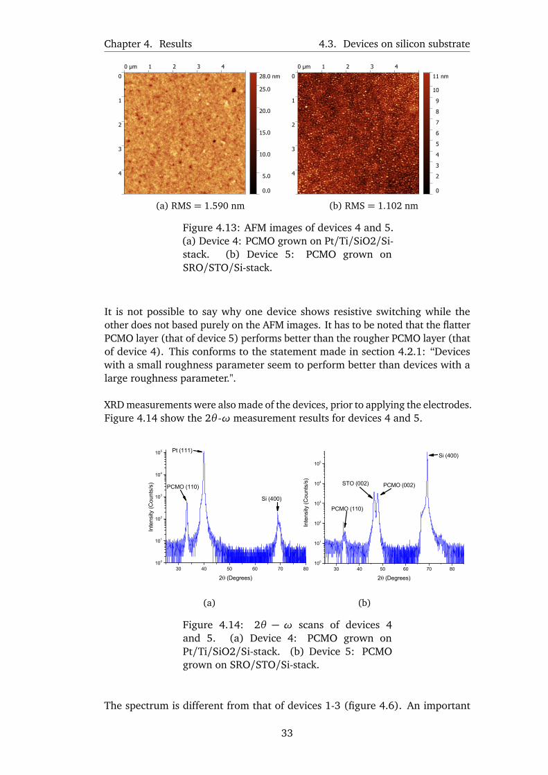
The PCMO layer of both devices was imaged using an AFM. These images areshown in figure 4.13.Both samples are relatively flat, and show no lines such as in figure 4.5a. ThePCMO layer of device 4, shown in figure 4.13a, shows some deep holes. ThePCMO layer of device 5 on the other hand shows no such holes, but does showmore peaks.
32
Chapter 4. Results 4.3. Devices on silicon substrate
0 µm 1 2 3 4
0
1
2
3
4
28.0 nm
0.0
5.0
10.0
15.0
20.0
25.0
(a) RMS = 1.590 nm
0 µm 1 2 3 4
0
1
2
3
4
11 nm
0
2
3
4
5
6
7
8
9
10
(b) RMS = 1.102 nm
Figure 4.13: AFM images of devices 4 and 5.(a) Device 4: PCMO grown on Pt/Ti/SiO2/Si-stack. (b) Device 5: PCMO grown onSRO/STO/Si-stack.
It is not possible to say why one device shows resistive switching while theother does not based purely on the AFM images. It has to be noted that the flatterPCMO layer (that of device 5) performs better than the rougher PCMO layer (thatof device 4). This conforms to the statement made in section 4.2.1: “Deviceswith a small roughness parameter seem to perform better than devices with alarge roughness parameter.".
XRD measurements were also made of the devices, prior to applying the electrodes.Figure 4.14 show the 2θ -ω measurement results for devices 4 and 5.
30 40 50 60 70 80100
101
102
103
104
105
Inte
nsity
(Cou
nts/
s)
2 (Degrees)
Si (400)
Pt (111)
PCMO (110)
(a)
30 40 50 60 70 80100
101
102
103
104
105
Inte
nsity
(Cou
nts/
s)
2 (Degrees)
Si (400)
STO (002) PCMO (002)
PCMO (110)
(b)
Figure 4.14: 2θ − ω scans of devices 4and 5. (a) Device 4: PCMO grown onPt/Ti/SiO2/Si-stack. (b) Device 5: PCMOgrown on SRO/STO/Si-stack.
The spectrum is different from that of devices 1-3 (figure 4.6). An important
33

4.3. Devices on silicon substrate Chapter 4. Results
difference between devices 4 and 5 is that device 4 only contains PCMO(110),while device 5 contains both (110) and –primarily– (002) oriented PCMO. De-vices 1-3 contain only (002) oriented PCMO, and show RS behaviour. Device 5also shows RS behaviour, device 4 does not. This suggests that the (110) orien-tation of the PCMO in device 4 might be the cause of the insufficient performance.
Kim uses a device that has a composition similar to that of device 4. This devicedoes show resistive switching. In Kim’s case, the PCMO is (112) oriented. Thissuggests either that the orientation of the PCMO in the device is crucial to deviceperformance, or that other aspects (such as the oxygen pressure during growth)are crucial to device performance.
Li states that the (110) and (001) orientations of PCMO have the best resis-tive switching properties due to their high density of manganese atoms.[29]
The FWHM of the rocking curves of the PCMO peaks in figure 4.14 is shown intable 4.5. Compared to the values of devices 1-3 (table 4.1), the values for devices4 and 5 are quite large, this is especially true for the FWHM of the PCMO(110)peak in device 4. This means that device 4 is less crystalline than the otherdevices.
Device FWHM ()4 PCMO(110) 3.88025 PCMO(002) 1.0685
Table 4.5: Full-width-half-maximum of therocking curves of the PCMO peaks for devices4 and 5.
Due to the low crystallinity, a leakage current can occur. While switching mightstill occur, the effect cannot be observed due to the leakage current. This leadsto current-voltage sweeps such as in figure 4.12a.
This means an argument can be made that the performance of the devices isnot dependent on the orientation of the PCMO layer, but dependent on the crys-tallinity of the PCMO layer. However, this argument fails based on the resultsfor devices 1-3, where large differences were observed in the performance of thedevices, yet the crystallinity of the devices was approximately the same for alldevices.
4.3.1 Stability measurements of device 5
To compare the functioning device (device 5) with devices 1-3, a stability mea-surement was performed, the results of which are shown in figure 4.15.The device performs quite well: the HRS/LRS-ratio does not converge to one forboth measurement methods. Instead, the value converges to approximately 3 incase of the pulse measurements and 3.5 in case of the sweep measurements.8
8Note that the sweep measurement only switches 200 times, while the pulse measurementswitches 1000 times. At n=200, the pulse measurement ratio was approximately 3.0-3.5.
34

Chapter 4. Results 4.3. Devices on silicon substrate
0 200 400 600 800 10000
10
20
30
40
50
HR
S/LR
S
Pulse number
0 500 10000
5000
10000
15000
20000
25000
Res
ista
nce
()
Pulse number
(a)
0 50 100 150 2000
10
20
30
40
50
60
HRS/LR
S
Sweep number
(b)
Figure 4.15: Stability measurements for de-vice 5 using the 50µm×50µm electrode. (a)Pulse stability, inset: progression of HRS andLRS resistance values. The same input signaltype as in section 4.2.2 was used. (b) Sweepstability.
There is some variation in the value of the HRS/LRS-ratio, mainly caused by afluctuation of the HRS resistance values. This should not necessarily be a problemfor application of the device as RRAM.
This is a good and important result. The device is able to resistively switchover a prolonged period of time, and is able to withstand numerous switchingoperations.
35

Chapter 5
Conclusion
Based on the results, discussed in section 4, the following can be concluded aboutthe devices researched in this report:
i. PCMO grown on a SRO/Nb-STO-stack shows interface type switching. Seefigure 4.1.
Concerning the influence of the oxygen pressure during PCMO growth:
ii. The level of oxygen in the PCMO layer is of influence on the resistiveswitching characteristics of the device. See figure 4.3 and figure 4.4.
iii. Devices with a small roughness parameter seem to perform better thandevices with a large roughness parameter. More measurements are neededto confirm this.
iv. The crystallinity of PCMO is dependent of the oxygen pressure duringgrowth. The crystallinity becomes better as the oxygen pressure is increased.See table 4.1.
v. The performance of RRAM devices is inversely related to the crystallinityof the PCMO.
vi. Stability is not influenced by the oxygen pressure during PCMO growth:devices 1-3 all converge to a HRS/LRS-ratio of one.
vii. Stability of the device increases when using the sweep or TSZ signal com-pared to a normal pulse signal.
Concerning the potential of devices 1-3 as commercial RRAM:
viii. The retention of information over time of device 3 is insufficient.
Concerning devices grown on silicon substrates:ix. Devices grown on a SRO/STO/Si-stack perform better than devices grown
on a Pt/Ti/SiO2/Si-stack. It is possible that this is caused by the orientationof the PCMO: (002) oriented PCMO seems to perform better than (110)oriented PCMO. Another possibility is that this is caused by the crystallinityof the PCMO. More measurements are required to verify which (if either)is true.
x. Performance of device 5 is better than any other device discussed in this
36

Chapter 5. Conclusion
report. The HRS/LRS-ratio converges to a value of approximately 3.0–3.5.
In short, the main conclusions are:
• PCMO-based RRAM devices are dependent on the oxygen pressure duringPCMO growth. Performance seems to increase as oxygen pressure decreases.The HRS/LRS-ratio of the device reaches high enough values to competewith flash memory. The retention and stability of the devices are notable to compete with flash memory. More research is needed to createcommercially viable devices.
• PCMO-based RRAM is compatible with current CMOS technology: a func-tioning PCMO-based RRAM device was grown on a silicon-based substrate.
37

Chapter 6
Discussion
6.1 Obstacles
Several obstacles were encountered during this research which might have influ-enced the results. In this section these obstacles will be described.
During the lift-off process of device 5 something went wrong, resulting in oddlyshaped electrodes. While these electrodes were not used for measurements, thiserror might still have influenced the results. The error was observed due to differ-ent surface colours. It is suspected that the PCMO layer was partly removed onsome areas of the device, taking (parts of) electrodes with it. Another possibilityis that there is still some acetone left on the surface of the device.
The resolution of the AFM was too low to image individual grains of the PCMOlayers. As grains are a good measure of the crystallinity of the PCMO layer, itwould have payed off to measure at a higher resolution.
As already shortly noted in chapter 4, the Keithley 4200-SCS placed some restric-tions on possible measurements. The maximum bin size of a signal that can beapplied by the Keithley is 4096 bins. This means long measurements cannot beperformed, unless the signal is manually executed several times. This resultsin rest periods between measurements in which the PCMO layer has time tostabilize, influencing the results.
A second problem with the Keithley is that there is no fixed time period perbin. This is especially a problem when a signal consists of pulses, as pulse dura-tion varies when using the Keithley. This could result in asymmetry in oxygenvacancy transport, and hence could result in an accumulation of oxygen vacan-cies at one electrode. Such an accumulation might cause a decrease in deviceperformance.
The Keithley also spends too much time processing each bin. Usable RRAMdevices should have SET and READ times of less than 100ns. The shortest SETand READ time achievable using the Keithley were approximately 8ms. Hence,the Keithley is unable to measure if devices switch fast enough to attain currentstandards.
38

Chapter 6. Discussion 6.2. Proposed further research
Connecting a function generator to the Keithley could solve these problems.A function generator can generate signals with a fixed frequency. Unfortunately,due to time restrictions, this has not been tested.
6.2 Proposed further research
In this section, several propositions for further research are discussed.
To determine the influence of the roughness parameter of the PCMO layer moredevices should be grown with different roughness parameters should be grownand their performance should be measured. The roughness parameter can bevaried by growing the PCMO layer at various oxygen pressures.
To fully determine the influence of the orientation of the PCMO layer on de-vice performance, more measurements should be performed. More devices withvarying orientations should be grown. This can be achieved by using differentlyoriented substrates.
As mentioned in the previous section, measurements with shorter SET, RESETand READ pulses should be done to see whether the device performs well withcurrent standards in electronics for pulse duration.
Finally, if a functioning RRAM device is found, the next step is to combinea single RRAM cell into a functioning structure consisting of many cells: a RRAMchip. A single RRAM cell is 1 bit, while current RAM technology consists of manygigabytes. Single RRAM cells will need to be connected in a cross-point arraystructure to create commercially viable RRAM.[11]
39

Acknowledgements
We would like to thank our supervisors, Dr. Zhaoliang Liao and Prof. Dr. Ing.Guus Rijnders, for their help and guidance during this project. We would alsolike to thank Dr. Minh Nguyen for his help in preparing the devices. Finally, wewould like to thank all other members of IMS for their help, we enjoyed beingpart of your group.
40

References
[1] A. Herpers. “Electrical characterization of manganite and titanate het-erostructures”. PhD thesis. Rheinisch-Westfälischen Technischen HochschuleAachen, 2014.
[2] T. Mikolajick et al. “FeRAM technology for high density applications”. In:Microelectronics Reliability 41.7 (2001), pp. 947 –950. DOI: 10.1016/S0026-2714(01)00049-X.
[3] Jian-Gang Zhu. “Magnetoresistive Random Access Memory: The Path toCompetitiveness and Scalability”. In: Proceedings of the IEEE 96.11 (2008),pp. 1786–1798. DOI: 10.1109/JPROC.2008.2004313.
[4] Panasonic. Panasonic Starts World’s First Mass Production of ReRAM MountedMicrocomputers. July 2013. URL: http://news.panasonic.com/press/news/official.data/data.dir/2013/07/en130730-2/en130730-2.html#1.
[5] R. Fackenthal et al. “19.7 A 16Gb ReRAM with 200MB/s write and 1GB/sread in 27nm technology”. In: Solid-State Circuits Conference Digest ofTechnical Papers (ISSCC), 2014 IEEE International. 2014, pp. 338–339. DOI:10.1109/ISSCC.2014.6757460.
[6] Y. Kim et al. “Influence of Deposition Temperature and Substrate Orienta-tion on the Microstructure of Pr0.7Ca0.3MnO3 Films Grown on PlatinumSubstrates by Using Pulsed Laser Deposition”. In: Journal of the KoreanPhysical Society 54 (2009), pp. 209–214.
[7] D. Kim et al. “Growth and characterization of Pr0.7Ca0.3MnO3 thin filmsfor resistance random acces memory”. In: Journal of the Korean PhysicalSociety 49 (2006), S557–S561. DOI: 10.3938/jkps.49.557.
[8] Z. Liao. “The effects of spatial confinement and oxygen stoichiometry oncomplex metal oxides”. PhD thesis. Louisiana State University, 2012.
[9] R. Waser et al. “Redox-Based Resistive Switching Memories –NanoionicMechanisms, Prospects, and Challenges”. In: Advanced Materials 21.25-26(2009), pp. 2632–2663. DOI: 10.1002/adma.200900375.
[10] H. Wong et al. “Metal-Oxide RRAM”. In: Proceedings of the IEEE 100.6(2012), pp. 1951–1970. DOI: 10.1109/JPROC.2012.2190369.
[11] A. Sawa. “Resistive switching in transition metal oxides”. In: MaterialsToday 11.6 (2008), pp. 28–36. DOI: 10.1016/S1369-7021(08)70119-6.
41

References References
[12] F. Pan et al. “Nonvolatile resistive switching memories-characteristics,mechanisms and challenger”. In: Progress in Natural Science: MaterialsInternational 20.0 (2010), pp. 1–15. DOI: 10.1016/S1002-0071(12)60001-X.
[13] Z. Liao et al. “Categorization of resistive switching of metal-Pr0.7Ca0.3MnO3-devices”. In: Applied Physics Letters 94.25 (2009). DOI: 10.1063/1.3159471.
[14] A. Sawa et al. “Hysteretic current-voltage characteristics and resistanceswitching at a rectifying Ti/Pr0.7Ca0.3MnO3 interface”. In: Applied PhysicsLetters 85.18 (2004), pp. 4073–4075. DOI: 10.1063/1.1812580.
[15] A. Herpers et al. “Spectroscopic Proof of the Correlation between Redox-State and Charge-Carrier Transport at the Interface of Resistively SwitchingTi/PCMO Devices”. In: Advanced Materials 26.17 (2014), pp. 2730–2735.DOI: 10.1002/adma.201304054.
[16] M. Ohring. “Chapter 3 - Thin-film evaporation processes”. In: MaterialsScience of Thin Films (Second Edition). Second Edition. San Diego: AcademicPress, 2002, pp. 95 –144. ISBN: 978-0-12-524975-1. DOI: 10.1016/B978-012524975-1/50006-9.
[17] R. Eason et al. “Multi-beam pulsed laser deposition for advanced thin-filmoptical waveguides”. In: Journal of Physics D: Applied Physics 3 (2014),p. 034007. DOI: 10.1088/0022-3727/47/3/034007.
[18] M. Ohring. “Chapter 4 - Discharges, plasmas, and ion-surface interactions”.In: Materials Science of Thin Films (Second Edition). Second Edition. SanDiego: Academic Press, 2002, pp. 145 –202. ISBN: 978-0-12-524975-1.DOI: 10.1016/B978-012524975-1/50007-0.
[19] P. Kelly and R. Arnell. “Magnetron sputtering: a review of recent devel-opments and applications”. In: Vacuum 56.3 (2000), pp. 159–172. DOI:10.1016/S0042-207X(99)00189-X.
[20] R. Jagtap and A. Ambre. “Overview literature on atomic force microscopy(AFM): Basic and its important applications for polymer characterization”.In: Indian Journal of Engineering and Materials Science 13 (2006), pp. 368–384.
[21] D. Leadley. X-Ray Diffraction. 2009. URL: http://www2.warwick.ac.uk/fac/sci/physics/current/postgraduate/regs/mpags/ex5/techniques/structural/xrd/.
[22] Fortgeschrittenpraktikum High Resolution X-Ray Diffraction. TechnischeUnversität München. 2009.
[23] M. Sardela. “X-ray analysis methods”. In: Advanced Materials Characteriza-tion Workshop, The Frederick Seitz Materials Research Laboratory–Universityof Illinois at Urbana-Champaign. 2008.
[24] D. Kim et al. “Effect of oxygen annealing on Pr0.7Ca 0.3MnO3 thin filmfor colossal electroresistance at room temperature”. In: Journal of AppliedPhsics 100 (2006), p. 093901. DOI: 10.1063/1.2364386.
42

References References
[25] K. Choi et al. “Microstructure and resistive switching behaviour of amor-phous Pr0.7Ca 0.3MnO3 films grown under various oxygen pressures”.In: ECS Solid State Letters 2.7 (2013), N21–N25. DOI: 10.1149/2.003307ssl.
[26] Y. Chen et al. “PCMO Device With High Switching Stability”. In: ElectronDevice Letters, IEEE 31.8 (2010), pp. 866–868. DOI: 10.1109/LED.2010.2050457.
[27] D. Panda and T. Tseng. “Perovskite Oxides as Resistive Switching Memories:A Review”. In: Ferroelectrics 471.1 (2014), pp. 23–64. DOI: 10.1080/00150193.2014.922389.
[28] C. Cheng et al. “High performance ultra-low energy RRAM with good reten-tion and endurance”. In: Electron Devices Meeting (IEDM), 2010 IEEE Inter-national. 2010, pp. 19.4.1–19.4.4. DOI: 10.1109/IEDM.2010.5703392.
[29] T. Li et al. PCMO thin film with resistance random access memory (RRAM)characteristics. US Patent 7,060,586. 2006.
43

Appendix A
Device information
The composition of the devices is given in detail in this appendix, the growthconditions of the PCMO layer for all devices is also given.
Device Ipulse fpulse Poxygen Tsubstrate
(J/cm2) (Hz) (mBar) (C)1 2.1 4 0.2 6702 (first 20nm) 2.1 4 0.2 6702 (80nm remainder) 2.1 4 10-3 6703 2.1 4 5× 10⁻⁵ 6504 2.1 4 10-3 6505 2.0 4 5× 10⁻⁵ 650
Table A.1: Growth conditions of the PCMOlayer in devices 1-5. Ipulse denotes the inten-sity of the pulse, fpulse denotes the pulse fre-quency, Poxygen denotes the oxygen pressureduring PCMO growth and Tsubstrate is the sub-strate temperature.
A.1 Devices 1-3
The layers in devices 1-3 all thicknesses. From top to bottom the layer com-position is as follows: Au(100nm)/Ti(16nm)/PCMO(100nm)/SRO(60nm)/Nb-STO(substrate, doped with Nb)/Ti(18nm)/Au(100nm).
SRO and PCMO were grown using PLD, Au and Ti were deposited using sput-tering. The properties of the Au and Ti deposition were the same for all devices.SRO depositon of devices 1-3 is similar: Poxygen = 0.3mBar, Tsubstrate = 670 C,Ipulse = 2.1 J/cm2 and fpulse = 4Hz.
The PCMO layers in devices 1-3 were grown under different conditions. Ta-ble A.1 provides an overview of the growth conditions for all devices.
44

Appendix A. Device information A.2. Device 4
A.2 Device 4
The composition of device 4 is as follows: Au(100 nm)/Ti(16 nm)/PCMO(100nm)/Pt/Ti/SiO2/Si(substrate). Deposition of Au and Ti layers was the same asfor devices 1-3. The conditions of the PCMO growth are shown in table A.1.
A.3 Device 5
Device 5 consists the following layers: Au(100nm)/Ti(16nm)/PCMO(100nm)/SRO(60nm)/STO/Si(substrate). Deposition of Au and Ti layers was the same asfor devices 1-3. The conditions of the PCMO growth are shown in table A.1.
45