Embed Size (px)
DESCRIPTION
aaa
Citation preview

�������� ����� ��
Structural and Optical Characterization of CdS/TiO2 Nanocomposite
Archana Maurya, Pratima Chauhan
PII: S1044-5803(11)00028-3DOI: doi: 10.1016/j.matchar.2011.01.014Reference: MTL 6930
To appear in: Materials Characterization
Received date: 22 May 2010Revised date: 17 January 2011Accepted date: 19 January 2011
Please cite this article as: Maurya Archana, Chauhan Pratima, Structural and OpticalCharacterization of CdS/TiO2 Nanocomposite, Materials Characterization (2011), doi:10.1016/j.matchar.2011.01.014
This is a PDF file of an unedited manuscript that has been accepted for publication.As a service to our customers we are providing this early version of the manuscript.The manuscript will undergo copyediting, typesetting, and review of the resulting proofbefore it is published in its final form. Please note that during the production processerrors may be discovered which could affect the content, and all legal disclaimers thatapply to the journal pertain.

ACC
EPTE
D M
ANU
SCR
IPT
ACCEPTED MANUSCRIPT
1
Structural and Optical Characterization of CdS/TiO2 Nanocomposite
Archana and Pratima Chauhan*
UGC Centre of Advanced Studies, Department of Physics, University of Allahabad,
Allahabad-211002, India.
E-mail: [email protected], [email protected]*
Abstract: Nanocomposites are advantageous because they can compensate for the
disadvantages of the individual component, and induce a synergistic effect, such as an
efficient charge separation and improvement of photostability. Present study reveals the
advantage of nanocomposite CdS/TiO2 over TiO2 which have been prepared by a simple
Co-precipitation method. The particle size of CdS/TiO2 estimated from X-ray diffraction
pattern comes out to be ~ 5.8 nm which is in good agreement with that of transmission
electron microscopy. High resolution transmission electron microscopy showed a
reduction in defect levels in the as prepared CdS/TiO2 nanocomposite in comparison to
TiO2. In our method titanium monoxide (TiO) phase has appeared at room temperature
against the earlier reports. Williamson-Hall plot analysis revealed the presence of tensile
strain in both the CdS/TiO2 and TiO2 samples. New Raman bands for rutile TiO2 have
also been observed which have not been previously reported. UV-visible study reveals
an enhanced absorption capability of the composite sample (~383.85 nm) in comparison
to pure TiO2 (~331.37 and 324.40 nm).The optical and electrical results have shown the
activation of the excited TiO2 in the presence of CdS.
Keywords: CdS/TiO2 Nanocomposite, Structural characterization, Optical
characterization.
ACC
EPTE
D M
ANU
SCR
IPT
ACCEPTED MANUSCRIPT
2
1 Introduction
In recent decades, nanostructured materials have attracted much attention due to their
special structure and excellent properties in optics, electronics, magnetics, chemistry, etc
[1-4]. Discovery and study of new materials whose properties can be tailored made
constitute the core development of solid state technology. Among various nanostructures,
including nanoparticles, nanotubes, nanorods and nanospheres; nanoparticles have
attracted wide attention due to their size-dependent properties. To fully harness the
potential capabilities of nanoparticles, we need to develop new methods to assemble them
into useful patterns or structures [5]. The development of new heterostructure is still a
challenging research subject. It’s challenging to modulate the properties by tailoring the
nucleation of one phase on the surface of the other [6].
In particular titanium dioxide (TiO2), as an important IV-VI group semiconductor,
has been widely applied in chemical industry [7], electronic industry [8, 9],
environmental protection [10], cosmetic industry [11], medical science [12], and so on. In
its pure form it is an n-type semiconductor with indirect band gaps of 3.2 eV for anatase
and 3.02 eV for rutile between the full oxygen 2p valence band and titanium 3d states at
the bottom of the conduction band. Wurtzite CdS, a direct band gap semiconductor with
band gap energy of 2.42 eV, is one of the first discovered semiconductors which have
promising applications in photochemical catalysis, gas sensor, detectors for laser and
infrared, solar cells, non-linear optical materials, various luminescence devices, and
optoelectronic devices [13-15]. One of the major factors that limit the efficiency of TiO2
photocatalysis is fast recombination of photogenerated electron/hole pairs [16].The large

ACC
EPTE
D M
ANU
SCR
IPT
ACCEPTED MANUSCRIPT
3
bandgap of TiO2 also significantly limits its light harvesting ability. To overcome this
drawback composites of two or more semiconducting materials with different band gaps
and band positions are made as this produces a long distance charge separated state with
electron and holes at sites far from each other.
Many methods have already been reported for generating CdS/TiO2 composites [17-21].
The preparation of CdS semiconducting quantum dots (QDs) by the chemical
precipitation method using Thioglycerol (TG) as the capping agent has already been
reported by our group [22]. Herein, we report an approach to efficiently synthesize
CdS/TiO2 composite nanoparticles by a simple co-precipitation method at room
temperature using CTAB as capping agent. Our experimental results clearly give the
evidence of an effective transfer of photogenerated electron from conduction band of CdS
to that of TiO2 and also show a good coupling between CdS and TiO2.
2 Experimental Procedures
2.1 Materials
Cadmium Sulphate (3CdSO4.8H2O) of M.W. = 769.49 and Min. Assay of 99.0 %,
Sodium Thiosulfate Pentahydrate (Na2S2O3 . 5H2O) of Molarity = 248.18 g/mol and Min.
Assay of 99.5-100.5 %, N-Cetyl-N ,N,N-trimethyl ammonium bromide (C19H42 Br N),
M.W. = 364.46, Minimum assay(iodometry)= 99.0% and Titanium (IV) chloride (TiCl4)
(anhydrous), M.W. = 189.71, density (d420
) = 1.729-1.730 and Min. Assay
(Argentometric) of 99.0 % had been used as starting materials. Ethanol (Merck), density
(d 20oC/20
oC) = 0.790-0.793 and purity of 99.9 % being commercially available. Double
distilled water had been used for all studies. All the used chemicals were analytic grade
reagents without further purification.

ACC
EPTE
D M
ANU
SCR
IPT
ACCEPTED MANUSCRIPT
4
2.1 Preparation of TiO2
Titanium tetrachloride was used as the starting material to prepare pure TiO2. 6.0 ml
titanium tetrachloride (TiCl4) was dropped into 100 ml double distilled water at room
temperature under vigorous stirring until the white fog disappeared. The solution
gradually turned into transparent soft gel, which continued to change with time, from
translucent to milky white. The process took 4–5 days, including the formation of gel (2–
3 days). The final gel was neutral (pH about 7). The gel was filtered under suction and
washed with distilled water until Cl− could not be measured (with 0.1 mol/l AgNO3). The
final white precipitate was washed with ethanol and double distilled water several times
and then dried at room temperature. In order to get finally divided TiO2 nanopowder the
samples were grinded in mortar with pestle.
2.3 Preparation of CdS/TiO2 nanocomposite
CdSO4 and Na2S2O3 were used as the reactant materials, and N-Cetyl-N, N, N-trimethyl
ammonium bromide (C19H42 Br N) (CTAB) was added as the capping agent. The
concentrations of CdSO4, Na2S2O3 and CTAB were 2mM, 100 mM and 0.2 M
respectively. In a simple procedure 100 ml aqueous solution of the reactants (CdSO4 and
Na2S2O3) and capping agent CTAB were prepared by Co- precipitation route. 6.0 ml of
TiCl4 was also slowly added dropwise to the solution under constant stirring. A colorless
solution was obtained which had been left at room temperature. A white precipitate
comes out after leaving the solution for 4 days. The solid product was then recovered by
filtration, washed with deionized water and air dried at room temperature. Finally divided
CdS/TiO2 nanopowder was obtained by grinding the samples in mortar and pestle. We

ACC
EPTE
D M
ANU
SCR
IPT
ACCEPTED MANUSCRIPT
5
have observed that the color of white precipitate turned to light yellow in the process of
drying.
Reaction mechanism:
The following reaction mechanism may be expected to occur between CdSO4 and
Na2S2O3 when CTAB was used as capping agent:
CdSO4 + Na2S2O3 + H2O CdS + Na2SO4 + H2SO4
Also, TiCl4 reacts with deionized water to give TiO2 as:
TiCl4 + 2H2O TiO2 + 4HCl
Finally, the reaction between CdS and TiO2 takes place as [23]:
CdS (e- + h
+) + TiO2 CdS (h
+) + TiO2 (e
-)
CdS (e- + h
+) + TiO2 (e
- + h
+) CdS (h
++ h
+) + TiO2 (e
- + e
-)
2.4 Characterization
Rigaku D-max XRD with Cu-Kα line (λ = 1.54A˚) was used for recording X-ray
diffraction (XRD) pattern operating at 30kV and 30mA in the 2 range 20o – 60
o.
Transmission electron microscopy (TEM) and high resolution transmission electron
microscopy (HRTEM) were performed by using Tecnai 30 G2 S-Twin electron
microscope operating at 300 kV accelerating voltage. Samples for TEM were prepared by
ultrasonically dispersing the product in ethanol, and the droplets were placed on carbon
coated Cu grids. Raman spectra were obtained using a RENISHAW invia Raman
spectrometer (RM2000) integrated with a Lica microscope. All the Raman spectra were
recorded by 514 nm Ar+ laser at room temperature. The UV-visible spectra were recorded
on Lambda 35 Perkin Elmer in the range 200-800 nm. Photoluminescence (PL) spectra of
the prepared samples were measured at room temperature using LS 55 Perkin Elmer

ACC
EPTE
D M
ANU
SCR
IPT
ACCEPTED MANUSCRIPT
6
spectrophotometer with 340 nm and 375 nm excitation line of Xenon discharge lamp,
equivalent to 20kV for 8µs duration with pulse width at half height < 10µs. Current-
voltage (I-V) curves of pure TiO2 and CdS/TiO2 pallets were taken under illumination
with a solar simulator (Oriel). The intensity of the Xenon lamp was adjusted to 100
mW/cm2.
3 Results and Discussion
Pure TiO2 and CdS/TiO2 composite were analyzed using XRD, TEM and HRTEM to
evaluate the structural characteristics. Figure 1 (a) shows the powder XRD pattern of pure
TiO2, which can be indexed to tetragonal rutile phase (JCPDS file no. 21-1276). In the
XRD spectra of CdS/TiO2 composite (Figure 1(b)) additional diffraction peaks marked
with #, $ and * also appears which corresponds to the powder diffraction patterns for
cubic CdS (JCPDS file no.772415), hexagonal CdS (JCPDS file no. 800006) and
titanium monoxide (TiO) (JCPDS file no.851061), respectively. The coexistence of both
the phases of CdS in the CdS/TiO2 composite attributes the particle size to be in the nano-
size regime [24-27]. In our case the TiO phase appears at room temperature itself against
the earlier report [28]. The possible explanation for this can be given by assuming the
formation of TiO molecules as a result of chemical reaction between Ti and TiO2 under
such experimental condition. The particle size (D) for both samples has been calculated
from (110) crystal plane located at 27.23o, using Debye-Scherrer formula ([D= 0.89 λ/ β
cos(θ)], where λ is the wavelength of X-ray used, β is the full width at half maximum
(FWHM) value and θ is the scattering angle).The calculated particle size of the pure TiO2
and CdS/TiO2 composite are ~ 6.3 nm and ~ 5.8 nm respectively. Furthermore, it is

ACC
EPTE
D M
ANU
SCR
IPT
ACCEPTED MANUSCRIPT
7
known that FWHM can be interpreted in terms of lattice strain and crystalline size [29]
which can be expressed by the following equation,
sin1cos
Where, ε and η are the effective particle size and the effective strain. The effective
particle size taking strain into account can be estimated by plotting β cosθ/λ versus sinθ/λ.
We have calculated the effective particle size and strain for both the samples by
Williamson-Hall plot, which are shown in Figure 2(a) and 2 (b). A negative slope in the
plot indicates the presence of compressive strain as has been reported by several authors
[30, 31]. In our case the appearance of positive slope has ensured the possibility of the
presence of tensile strain [32]. Williamson-Hall plot gives lattice strain of 4.29 % for pure
TiO2 and 4.97 % for CdS/TiO2. Effective particle size calculated by Williamson-Hall plot
for TiO2 and CdS/TiO2 are ~ 7.5 nm and ~ 5.6 nm respectively. These particle size values
appear to be in good agreement with the one calculated by Scherrer formula.
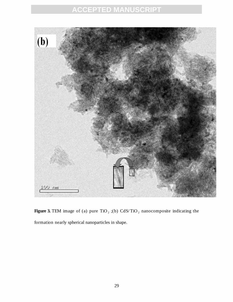
TEM image of both the samples are shown in Figure 3(a) and 3(b)
respectively. These figures correspond to the formation of uniform spherical
nanoparticles with slight prolate deviation. Some aggregations among the nanoparticles
have been observed for the case of CdS/TiO2. The particle size of TiO2 lies in the range
of ~ 2.79 to 6.55 nm whereas of CdS/TiO2 ~ 3.49 to 5.08 nm. These results are found to
be consistent with the XRD and Williamson-Hall plot results. Figure 4(a) and 4(b) show
the HRTEM images of the prepared pure TiO2 and CdS/TiO2 composite. The images
clearly show lattice fringes indicating good crystallinity of the samples. From figure 4(a),
the lattice fringes most frequently observed at d0.33, d0.22, d0.25 and d0.17 correspond to the
(1 1 0), (1 1 1), (1 0 1) and (2 1 1) crystal planes of pure rutile phase of TiO2. The

ACC
EPTE
D M
ANU
SCR
IPT
ACCEPTED MANUSCRIPT
8
formation of some planar defects including twinned crystal plane and line imperfection
has also been observed in TiO2. These defect sites act as trap states for the electrons and
holes. Meanwhile, the HRTEM image of composite CdS/TiO2 (figure 4(b)) shows the
formation of mixed phases of crystal planes. The most frequently observed fringes at
d0.28, d0.25, and d0.19 corresponds to (0 1 5), (1 0 9) and (2 1 1) crystal plane of TiO and
d0.33 is the (1 1 0) crystal plane of rutile TiO2. However, in addition we have also
observed fringes of cubic CdS at d0.15 corresponding to (2 0 0) crystal plane and fringes
of hexagonal CdS at d0.34 which corresponds to (0 0 2) crystal plane. Thus CdS particles
being in close contact with TiO2 particles are easily observed in HRTEM images of
CdS/TiO2, indicating a good coupling between the distinct phase domains of CdS and
TiO2. A reduction in planar defect can easily be seen from the HRTEM image of
CdS/TiO2.
Young-wook Jun, Yung-tak Jang et al. have reported that nanocrystals can have
potentially a variety of crystalline phases from isotropic structures of cubic to anisotropic
structure of hexagonal or monoclinic [33]. Among various crystalline phases, the stable
phase of materials is highly dependent on its environmental conditions such as
temperature and choice of capping molecules. The surface energy can significantly
modify the phase relationship when the particle size is very small. Adsorption of ions
onto surfaces and lattice strain can further modify phase relations through their effect on
surface energy. Given the particle size effect on the phase relationship and the small
volumes of the materials involved; formation of titanium monoxide and rutile TiO2 phase
from anatase TiO2, and hexagonal and cubic phases of CdS may be possible by a solid
state reaction. The nucleation of rutile may be promoted by the fact that twin surfaces
ACC
EPTE
D M
ANU
SCR
IPT
ACCEPTED MANUSCRIPT
9
contain a unit cell of rutile. This surface can act as a nucleus, and may grow as a stable or
nearly stable phase, driven by random fluctuations. From the above discussion we may
arrive to an important conclusion that oriented attachment and growth can lead to the
formation of planar defects including twin planes and other interfaces. The structurally
different regions may serve as nucleation site for new phases.
Typical Raman spectra of TiO2 and CdS/TiO2 samples at room
temperature using 514.5 nm excitation wavelength of Ar+ laser are shown in Figure 5. To
see the differences between the spectra more clearly, the wavenumbers with their
corresponding full width half maxima (FWHM) are given in table 1. Rutile (tetragonal,
P42/mnm) consist of two units and four Raman active modes at 143 cm-1
(B1g), 447 cm-
1(Eg), 612 cm
-1(A1g) and 826 cm
-1(B2g) [34]. As can be seen from the table that the
Raman bands in our case occurs at position of higher wavenumber side compared to that
of the reported value for rutile TiO2. Since, XRD pattern has confirmed the pure rutile
phase of TiO2, with no significance of any other phase, all the observed Raman bands can
be assigned to the Raman bands of the rutile single phase. These Raman bands of rutile
TiO2 observed in our case have not been previously reported to the best of our
knowledge. The peak at 220.08 cm-1
in CdS/TiO2 nanocomposite resembles the peak of
CdS as observed by D. Mohanta et al. [35]. Earlier reports show that the rutile peaks of
TiO2 appear at higher temperature [36]. But at high temperature the particle size also
increases and exhibit a large frequency redshift with remarkable decrease in linewidth
[37] .Hyun Chul Choi et al, have reported that for TiO2 the Raman band shifts towards
higher wavenumber and their intensities relatively decrease as the particle size decreases
[38]. The same result has been reported by several authors for different types of

ACC
EPTE
D M
ANU
SCR
IPT
ACCEPTED MANUSCRIPT
10
nanoparticles [39-44]. The variation in Raman band can be attributed due to the small
size and room temperature preparation of the nanoparticles. Furthermore, while
comparing the shifts in band position between TiO2 and CdS/TiO2 we observe that for
CdS/TiO2 nanocomposite the Raman band at 262.28 cm-1
shifts to 263.97 cm-1
and
436.82 cm-1
shifts to 437.86 cm-1
. It has been reported earlier that such a blue shift could
be attributed to phonon confinement caused by a decrease in crystal size [45] or an
increased surface strain of CdS/TiO2 caused by the adsorption of surfactant [46].
However, the band at 594.26 cm-1
possess less variation (594.14 cm-1
) and that at 687.07
cm-1
suffers large variation (684.72 cm-1
) towards lower wavenumber for the case of
CdS/TiO2. These effects occur because CdS/TiO2 sample contains a range of particles
from ~ 3.49 to 5.08 nm as obtained from TEM analysis. When the particle size decreases
towards the nanometer scale a volume contraction occurs within the nanoparticle due to
the size-induced radial pressure and this leads to increase in the force constants as a result
of the decrease in the interatomic distances. In vibrational transitions, the wavenumber
vary approximately in proportion to k1/2
, where k is the force constant. Consequently, the
Raman band shifts towards higher wavenumber due to the increasing force constants
[47]. The contraction effect also induces a decrease in the vibrational amplitudes of the
nearest neighbour bonds due to the increase of the static disorder and thermal vibrational
disorder of a material [48, 49]. This decrease in vibrational amplitude with decrease in
particle size is responsible for the intensity variation of the Raman bands observed in
figure 5. Also, as far as FWHM value is considered for composite sample we observe its
value decreases for some band positions and increases for others. H. Cao et al. have
reported the decrease of FWHM to the improvement of the crystallinity of the

ACC
EPTE
D M
ANU
SCR
IPT
ACCEPTED MANUSCRIPT
11
synthesized material [50]. A measurement of FWHM value implies that the crystallinity
of composite sample is somehow less perfect than TiO2 but not in great amount.
O ptical properties of nanocomposite could be different from the
corresponding components. Also, different sizes and shapes have different effect on
the properties of the material as well. The variation of any physical properties
caused by the incorporation of CdS in TiO 2 can be elucidated by considering the
optical properties: UV-visible and PL spectroscopy.
The UV-visible absorption spectra of TiO2 and CdS/TiO2 composite samples are shown
in Fig.6 (a) and 6 (b) respectively. The absorption band gap energy can be determined by
the following equation [51]:
(αhν)n = B (hν – Eg)
Where hυ is the photon energy, α is the absorption coefficient, B is a constant relative to
the material and n is a value that depends on the nature of transition (2 for a direct
allowed transition, 2/3 for direct forbidden transition, and 1/2 for indirect allowed
transition). However, in the nanocrystal there may be some deviation from a bulk-like
transition. So, we have determined the nature of transition by the equation [52]
d{ln(αhν)}/d(hν) = n/(hν − Eg) (2)
Figure 7(a) and 7 (b) show the differential graphs of TiO2 and CdS/TiO2 obtained by
considering equation (2). We observed that absorption edge of CdS/TiO2 nanocomposite
occurs at energy of 3.22 eV (~383.85 nm) which matches neither the optical edge of bulk
rutile TiO2, (3.02 eV) (~409 nm) nor that of bulk CdS (2.42 eV) (~508 nm). Also, as far
as prepared pure TiO2 sample is considered, the absorption edge gives double transitions
at the energies of 3.73 eV (~331.37 nm) and 3.81 eV (~324.40 nm) which is larger than

ACC
EPTE
D M
ANU
SCR
IPT
ACCEPTED MANUSCRIPT
12
the value of 3.02 eV for bulk rutile TiO2 suggesting a possibility of degeneracy of
valence band in TiO2. It can be seen that the absorption of both the samples lies in the
ultraviolet region and the absorption edge is less than 400 nm. The enhanced absorption
capability of CdS/TiO2 nanocomposite in comparison to pure TiO2 in the UV-visible
region of the spectra is attributed due to a coupling between TiO2 and CdS
heterostructure.
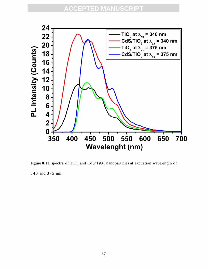
Figure 8 shows the PL spectra of TiO 2 and CdS/ TiO 2 nanocomposite at excitation
wavelengths of 3 4 0 and 3 7 5 nm. For PL measurements an excitation wavelength of
3 4 0 nm has been selected since it is close to the maximum absorption spectra for
pure TiO 2. Band gap (Eg) excitation originates a broad emission band centered at
4 0 5 nm (3 .0 5 eV) in addition to two minor bands at 45 7 and 49 8 nm for both
the cases of pure TiO 2 and CdS/ TiO 2. It has been reported earlier that there is no
PL peak in pure anatase phase, but a weak PL peak in the rutile phase of TiO 2 [5 3 ,
5 4 ]. But in our case we have observed a fine PL for rutile phase TiO 2 and an
enhanced PL for the CdS/ TiO 2 which is contradicting the earlier reports. Also, it
can be seen that the main peak in the high-energy side and minor peaks in the low-
energy side remain at same position upon combination of TiO 2 with CdS. O nly the
overall intensity of PL gets increased. Several authors have reported quenching
behavior of CdS/ TiO 2 nanocomposite which indicates deactivation of the excited
CdS in the presence of TiO 2 via electron transfer to TiO 2 nanoparticles [5 5 - 5 9 ].
An enhanced PL intensity in our case can be attributed to an activation of the
excited TiO 2 in the presence of CdS rather than deactivation. Also, on increasing
ACC
EPTE
D M
ANU
SCR
IPT
ACCEPTED MANUSCRIPT
13
excitation wavelength 37 5 nm, not only the number of minor PL peaks in the low-
energy side decreases, but the peak position also shifts as well. This happens because
at lower energies, several different recombination pathways involving trap states
exist viz.; (1 ) recombination of a conduction band (CB) electron with a trapped
hole; (2 ) recombination of trapped electron with a valence band (VB) hole; (3 )
recombination of a trapped electron with a trapped hole. The region is referred to
as trap-state PL [6 0 ].
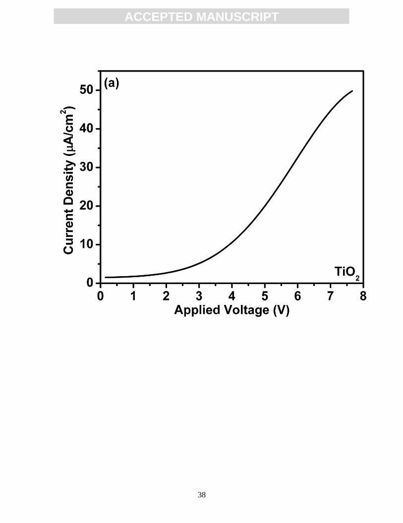
The current density-voltage (J-V) curves of the pure TiO 2 and
CdS/ TiO 2 under illumination are shown in Figure 9 (a) and 9 (b). It is observed
that larger values of Jsc occur for CdS/ TiO 2 nanocomposite, which varied from
0 .6 5 to 9 .7 4 mA/ cm2,indicating that the composite sample is more conductive.
The values of Jsc for TiO 2, on the other hand, varied in the range of microamperes
from 1 .6 5 to 4 9 .89 μA/ cm2,which can be attributed due to the high molecular
defect density and large electron-hole recombination. Considering that the
crystallite size and oxygen vacancies are similar for both the samples, the difference
in electrical behavior of CdS/ TiO 2 with respect to that of TiO 2 can be attributed
due to a mixture of crystalline phases. It has been established that in the CdS/ TiO 2
composite, CdS and TiO 2 serve for light collection and photoinduced charge
transfer respectively. The carrier of CdS can be promoted from the valence band to
the conduction band by light excitation due to its direct band gap in the visible
wavelength region. The photogenerated electrons in CdS are transferred into the
TiO 2 particles while the hole remains in the CdS particles (Figure 1 0 ). This helps in

ACC
EPTE
D M
ANU
SCR
IPT
ACCEPTED MANUSCRIPT
14
charge separation by isolating electron and hole in two distinct particles and hence
causing an increased Jsc in case of CdS/ TiO 2.
4 Conclusions
Present paper demonstrates the detailed study of the structural and optical
properties of pure TiO 2 and that of CdS/ TiO 2 composite nanoparticles. XRD
investigation has confirmed the formation of CdS/ TiO 2 composite. The particle size
of pure TiO 2 and CdS/ TiO 2 composite synthesized at room temperature are ~ 6 .3
nm and ~ 5 .8 nm. TEM image of pure TiO 2 and CdS/ TiO 2 shows the formation of
nearly spherical nanoparticles. The particle size as estimated by Williamson-Hall plot
also appeared to be consistent with the XRD and TEM results. The appearance of
positive slope has ensured the possibility of the presence of tensile strain. New Raman
bands for rutile TiO2 is observed in our case which has not been previously reported to
the best of our knowledge. Such variation in Raman band could be attributed due to
phonon confinement caused by decrease in crystal size. UV-visible study reveals an
enhanced absorption capability of the composite sample in comparison to TiO2 in the
UV-visible region of the spectra. PL characterization attributes an activation of the
excited TiO 2 in the presence of CdS rather than deactivation. An enhanced Jsc for
CdS/ TiO 2 indicates that the composite sample is more conductive than TiO 2.
Electrical and optical properties of CdS / TiO 2 nanocomposite reveals that sample
could have its major application in white light nanodevices such as light emitting
diodes (LEDs) and photocatalysis.
Acknowledgement

ACCE
PTED
MAN
USCR
IPT
ACCEPTED MANUSCRIPT
15
The authors wish to thank to Prof. A.C. Pandey, Nanotechnology Application Center,
University of Allahabad, Allahabad, India for providing XRD, TEM, HRTEM, RAMAN
and PL facilities. We are thankful to Prof. Ram Gopal, Deptt of Physics, University of
Allahabad, Allahabad, India for providing the UV-Visible absorption facility. One of the
authors Ms Archana would like to acknowledge UGC for granting research fellowship.
References
[1] Y.N. Xia, P.D. Yang, Y.G. Sun, Y.Y. Wu, B. Mayers, B. Gates,Y.D. Yin, F. Kim,
H.Q. Yan, “One-Dimensional Nanostructures: Synthesis, Characterization, and
Applications”,Adv. Mater. 15, 353 (2003).
[2] Xiaobo Chen and Samuel S. Mao, “Titanium Dioxide Nanomaterials: Synthesis,
Properties, Modifications, and Applications”, Chem. Rev., 2007, 107 (7), pp 2891–2959.
[3] Meng Ni, Michael K.H. Leung_, Dennis Y.C. Leung, K. Sumathy, “A review and
recent developments in photocatalytic water-splitting using TiO2 for hydrogen
production”, Renewable and Sustainable Energy Reviews 11 (2007) 401–425.
[4] S.J. Pearton, D.P. Norton, K. Ip, Y.W. Heo, T. Steiner, “Recent progress in
processing and properties of ZnO”, Superlattices and Microstructures 34 (2003) 3–32

ACC
EPTE
D M
ANU
SCR
IPT
ACCEPTED MANUSCRIPT
16
[5] Prashant Kumar, “Directed Self-Assembly: Expectations and Achievements”,
Nanoscale Res Lett (2010) 5:1367–1376
[6] Le Wang, Hongwei Wei, Yingju Fan, Xinzheng Liu, Jinhua Zhan, “Synthesis, Optical
Properties, and Photocatalytic Activity of One-Dimensional CdS@ZnS Core-Shell
Nanocomposites”, Nanoscale Res Lett (2009) 4:558–564.
[7] L. Caballero, K.A. Whitehead, N.S. Allen, J. Verran, “Photoinactivation of
Escherichia coli on acrylic paint formulations using fluorescent light”, Dyes and
Pigments 86 (2010) 56-62
[8] Shahed U. M. Khan, Mofareh Al-Shahry, William B. Ingler Jr., “Efficient
Photochemical Water Splitting by a Chemically Modified n-TiO2”, Science 27 September
2002: Vol. 297. no. 5590, pp. 2243 - 2245
[9] Hou, K.,; Tian, B.Z,; Li, F.Y.,; Bian, Z.Q.,; Zhao, D.Y.,; Huang, C.H, “Highly
crystallized mesoporous TiO2 films and their applications in dye sensitized solar cells”,
Volume 15 (24), p.2414-2420, (2005).
[10] Xiaoshan Zhu a, Yung Chang b,*, Yongsheng Chen, “Toxicity and bioaccumulation
of TiO2 nanoparticle aggregates in Daphnia magna”, Chemosphere 78 (2010) 209–215
[11] Jérôme Labille, Jinghuan Feng , Céline Botta , Daniel Borschneck , Magali Sammut
, Martiane Cabie , Mélanie Auffan, Jérôme Rose, Jean-Yves Bottero, “Aging of TiO2
nanocomposites used in sunscreen. Dispersion and fate of the degradation products in
aqueous environment”, Environmental Pollution 158 (2010) 3482-3489.
[12] D.M. Gonçalves, S. Chiasson, D. Girard, “Activation of human neutrophils by
titanium dioxide (TiO"2) nanoparticles”, Toxicology in Vitro 24 (2010) 1002–1008.

ACC
EPTE
D M
ANU
SCR
IPT
ACCEPTED MANUSCRIPT
17
[13] Ritesh Agarwal, Carl J. Barrelet and Charles M. Lieber, “Lasing in Single Cadmium
Sulfide Nanowire Optical Cavities”, Nano Lett., 2005, 5 (5), pp 917–920.
[14] Ren-Min Ma, Lun Dai and Guo-Gang Qin, “High-Performance Nano-Schottky
Diodes and Nano-MESFETs Made on Single CdS Nanobelts”, Nano Lett., 2007, 7 (4), pp
868–873.
[15] J. S. Jie,
W. J. Zhang, Y. Jiang,
X. M. Meng,
Y. Q. Li and S. T. Lee,
“Photoconductive Characteristics of Single-Crystal CdS Nanoribbons”, Nano Lett., 2006,
6 (9), pp 1887–1892.
[16] Yi Xie, Sung Hwan Heo, Seung Hwa Yoo, Ghafar Ali and Sung Oh Cho, “Synthesis
and Photocatalytic Activity of Anatase TiO2 Nanoparticles-coated Carbon Nanotubes”,
Nanoscale Res Lett (2010) 5:603–607.
[17] Zhai Jiwei, Zhang Liangying, Yao Xi and Shi Wensheng, “Sol–gel preparation and
optical non-linearity of CdS microcrystallite-doped SiO2–TiO2 thin films”,JOURNAL
OF MATERIALS SCIENCE LETTERS 18 (1999) 1107 – 1109.
[18] Won-Wook So, Kwang-Je Kim, Sang-Jin Moon, "Photo-production of hydrogen
over the CdS-TiO2 nano-composite particulate films treated with TiCl4," International
Journal of Hydrogen Energy, vol. 29 (2004), no. 3, pp. 229-234.
[19] Ming-Chi Hsua, Ing-Chi Leu, Yu-Ming Sun, Min-Hsiung Hon, “Fabrication of
CdS@TiO2 coaxial composite nanocables arrays by liquid-phase deposition”, Journal of
Crystal Growth 285 (2005) 642–648.

ACC
EPTE
D M
ANU
SCR
IPT
ACCEPTED MANUSCRIPT
18
[20] Jing-yuWang, Zhi-hong Liu, Qi Zheng, Zhi-keHe and Ru-xiu Cai, “Preparation of
photosensitized nanocrystalline TiO2 hydrosol by nanosized CdS at low temperature”,
Nanotechnology 17 (2006) 4561–4566.
[21] Hyunwoong Park, Wonyong Choi, Michael R. Hoffmann, “Effects of the
preparation method of the ternary CdS/TiO2/Pt hybrid photocatalysts on visible light-
induced hydrogen production” J. Mater. Chem., 2008, 18, 2379–2385.
[22] Vineet Singh and Pratima Chauhan, “Structural and optical characterization of CdS
nanoparticles prepared by chemical precipitation method”, Journal of Physics and
Chemistry of Solids 70 (2009) 1074–1079.
[23] Y. Bessekhouad et al. “UV–vis versus visible degradation of Acid Orange II in a
coupled CdS/TiO2 semiconductors suspension” Journal of Photochemistry a
Photobiology A: Chemistry 183 (2006) 218-224.
[24] Patrícia M.A. de Farias, Beate S. Santos, Ricardo L. Longo, Ricardo Ferreira, Carlos
L. Cesar, “CdS nanoparticles: structural and energetical correlations”, Materials
Chemistry and Physics 89 (2005) 21–27
[25] Yu Jun Yanga,_, Bao Jian Xiang, “Wet synthesis of nearly monodisperse CdSe
nanoparticles at room temperature”, Journal of Crystal Growth 284 (2005) 453–458
[26] Jaehyeong Lee, “Raman scattering and photoluminescence analysis of B-doped CdS
thin films”, Thin Solid Films 451 –452 (2004) 170–174
[27] Vineet Singh, Prashant K. Sharma, Pratima Chauhan, “Surfactant mediated phase
transformation of CdS nanoparticles”, Materials Chemistry and Physics 121 (2010) 202–
207.

ACC
EPTE
D M
ANU
SCR
IPT
ACCEPTED MANUSCRIPT
19
[28] K O Hara, E Yamasue, H Okumura and K N Ishihara, “Formation of metastable
phases by high-energy ball milling in the Ti-O system”, Journal of Physics: Conference
Series 144 (2009) 012021.
[29] G.K Williamson and W.H Hall, “X-ray line broadening from filed aluminium and
wolfram”, Acta Metal 1 (1953), p. 22-31.
[30] Rajeev R Prabhu and M Abdul Khadar, “Study of optical phonon modes of CdS
nanoparticles using Raman spectroscopy”, Bull. Mater. Sci., Vol. 31, No. 3, June 2008,
pp. 511-515.
[31] Feng Gu, Shu Fen Wang, Meng Kai Lü, Guang Jun Zhou, Dong Xu, and Duo Rong
Yuan “Photoluminescence Properties of SnO2 Nanoparticles Synthesized by Sol−Gel
Method”, J. Phys. Chem. B, 2004, 108 (24), pp 8119–8123.
[32] V. Senthilkumar, P. Vickraman, M. Jayachandran, C. Sanjeeviraja, “Structural and
electrical studies of nano structured Sn1-x Sbx O2 (x = 0.0, 1, 2.5, 4.5 and 7 at %) prepared
by co-precipitation method”, J. Mater Sci: Mater Electron (2010) 21: 343-348.
[33]Young-wook Jun, Yung-tak Jang, and Jinwoo Cheon, “Nanocrystals and Their
Biomedical Application”,Bull. Korean Chem. Soc. 2006, Vol. 27, No. 7,961-971.
[34] S. P. S. Porto, P. A. Fleury, and T. C. Damen, “Raman Spectra of TiO2, MgF2, ZnF2,
FeF2, and MnF2”, Phys. Rev. 154, 522–526 (1967).
[35] D. Mohanta, G. A. Ahmed, and A. Choudhury, “Spectroscopic Investigation of
Carrier Confinement and Surface Phonon Detection in Polymer Embedded CdS Quantum
Dots Systems”, CHINESE JOURNAL OF PHYSICS, 2004 VOL. 42, NO. 6

ACC
EPTE
D M
ANU
SCR
IPT
ACCEPTED MANUSCRIPT
20
[36] Suryanarayanan, R.; Naik, V. M.; Kharel, P.; Talagala, P.; Naik, R ,
“Ferromagnetism at 300 K in spin-coated films of Co doped anatase and rutile-TiO2”,
Solid State Communications, Volume 133, Issue 7, 2005, Pages 439-443.
[37] W F Zhang, Y L He, M S Zhang, Z Yin† and Q Chen,“Raman scattering study on
anatase TiO2 nanocrystals”, J. Phys. D: Appl. Phys. 33 (2000) 912–916
[38] Hyun Chul Choi, Young Mee Jung, Seung Bin Kim, “Size effects in the Raman
spectra of TiO2 nanoparticles”, Vibrational pectroscopy 37 (2005) 33-38.
[39] I.H. Campbell, P.M. Fauchet, “The effects of microcrystal size and shape on the one
phonon Raman spectra of crystalline semiconductors”, Solid State Commun. 58 (1986)
739-741.
[40] V. R. Palkar, S. C. Purandare, P. Ayyub, and R. Pinto, “Si induced size effects in
ferroelectric PbTiO2”, J. Appl. Phys. 87 (2000) 462-466.
[41] J. Zuo, C. Xu, X. Liu, C. Wang, C. Wang, Y. Hu, Y. Qian, “Study of the Raman
spectrum of nanometer SnO2”, J. Appl. Phys. 75 (1994) 1835-1836.
[42] R.G. Schlecht, H.K. Bo¨ckelmann, “Raman Scattering from Microcrystals of MgO”,
Phys. Rev. Lett. 31, 930–932 (1973).
[43] J. Zuo, C. Xu, L. Zhang, B. Xu, R. Wu, “Sb-induced size effects in ZnO
nanocrystallites”, J. Raman Spectrosc. 32 (2001) 979-981.
[44] B. Schreder, C. Dem, M. Schmitt, A. Materny, W. Kiefer, U. Winkler, E. Umbach,
“Raman spectroscopy of II-VI semiconductor nanostructures: CdS quantum dots”, J.
Raman Spectrosc. 34 (2003) 100-103.
[45] D. Bersani, P. P. Lottici, Xing-Zhao Ding, “Phonon confinement effects in the
Raman scattering by TiO2 nanocrystals”, Appl. Phys. Lett. 72 (1), 73, 1998.

ACC
EPTE
D M
ANU
SCR
IPT
ACCEPTED MANUSCRIPT
21
[46] C.Y. Xu, P.X. Zhang, L. Yan, J., “Blue shift of Raman peak from coated TiO2
nanoparticles”,Raman Spectrosc. 32, 862 (2001).
[47] S. Hayashi, H. Kanamori, “Raman scattering from the surface phonon mode in GaP
microcrystals” Phys. Rev. B 26, 7079–7082 (1982).
[48] J. Rockenberger, L. Troger, A. Kornowski, T. Vossmeyer, A. Eychmuller, J.
Feldhaus, H. Weller, “EXAFS Studies on the Size Dependence of Structural and
Dynamic Properties of CdS Nanoparticles”, J. Phys. Chem. B, 1997, 101 (14), pp 2691–
2701.
[49] M.A. Marcus, M.P. Andrews, J. Zegenhagen, A.S. Bommannavar, P. Montano,
“Structure and vibrations of chemically produced Au55 clusters”, Phys. Rev. B 42, 3312–
3316 (1990).
[50] H. Cao, G. Wang, S. Zhang, X. Zhang, D. Rabinovich, “Growth and Optical
Properties of Wurtzite-Type CdS Nanocrystals”, Inorg. Chem., 2006, 45 (13), pp 5103–
5108.
[5 1 ] Salem AM, Soliman Selim M., “Structure and optical properties of chemically
deposited Sb2S3 thin films”, J Phys D Appl Phys 2001; 34:12–7.
[5 2 ] R Maity and K K Chattopadhyay, “Synthesis and optical characterization of
ZnS and ZnS:Mn nanocrystalline thin films by chemical route”, Nanotechnology 15
(2004) 812–816.
[53] K. Chandrasekaran and J. K. Thomas, “Photochemical reactions of amorphous and
crystalline titanium dioxide powder suspensions in water”, Chem. Soc., Faraday Trans.
1, 1984, 80, 1163 – 1172.

ACC
EPTE
D M
ANU
SCR
IPT
ACCEPTED MANUSCRIPT
22
[54] L. G. J. de Haart, G. Blasse, “The observation of exciton emission from rutile single
crystals”, J. Solid State Chem. 1986, 61 ,135-136.
[55] H. Fujii, K. Inata, M. Ohtaki, K. Eguchi and H. Arai, “Synthesis of TiO2/CdS
nanocomposite via TiO2 coating on CdS nanoparticles by compartmentalized hydrolysis
of Ti alkoxide” JOURNAL OF MATERIALS SCIENCE 36 (2001) 527– 532.
[56] Hong Li, Baolin Zhu, Yunfeng Feng, Shurong Wang, Shoumin Zhang, Weiping
Huang, “Synthesis, characterization of TiO2 nanotubes-supported MS (TiO2NTs@MS,
M = Cd, Zn) and their photocatalytic activity”, Journal of Solid State Chemistry 180
(2007) 2136–2142.
[57] H. Park, W. Choi and M. R. Hoffmann, “Effects of the preparation method of the
ternary CdS/TiO2/pt hybrid photocatalysts on visible light-induced hydrogen
production”,J. Mater. Chem., 2008, 18, 2379.
[58] M. W. Xiao, L. S. Wang, Y. D. Wu, X. J. Huang and Z. Dang, “Preparation and
characterization of CdS nanoparticles decorated into titanate nanotubes and their
photocatalytic properties”, Nanotechnology, 2008, 19, 015706.
[59] Dinakaran Kannaiyan, Eunhye Kim, Nayoun Won et al,“On the synergistic coupling
properties of composite CdS/TiO2 nanoparticle arrays confined in nanopatterned hybrid
thin films”, J. Mater. Chem., 2010, 20, 677–682.
[60] J.L. Blackburn, D. C. Selmarten et al. “Electron and Hole Transfer from Indium
Phosphide Quantum Dots”, J. Phys. Chem. B 2005, 109, 2625-2631.

ACC
EPTE
D M
ANU
SCR
IPT
ACCEPTED MANUSCRIPT
23
Figure Caption
Figure 1. X-ray dif f raction patterns of pure rutile TiO 2, and CdS/ TiO 2
nanocomposite prepared via simple Co- precipitation method.
Figure 2. Williamson-Hall plots of (a) pure TiO2 and (b) CdS/TiO2 for the size and strain
analysis of the prepared nanoparticles.
Figure 3. TEM image of (a) pure TiO 2 ;(b) CdS/ TiO 2 nanocomposite indicating the
formation nearly spherical nanoparticles in shape.
Figure 4. HRTEM image of (a) TiO 2 showing crystal planes of pure rutile phase, and
(b) CdS/ TiO 2 nanocomposite showing crystal planes of rutile (R) titanium dioxide

ACC
EPTE
D M
ANU
SCR
IPT
ACCEPTED MANUSCRIPT
24
(TiO2), titanium monoxide (TiO), and hexagonal (H) and cubic (C) cadmium sulfide
(CdS).
Figure 5. Raman spectra of TiO2 and CdS/TiO2 composite sample prepared via Co-
precipitation method.
Figure 6. Comparison of UV-visible absorption spectra between (a)TiO 2 and (b)
CdS/ TiO 2. The nominal concentration of TiCl4 in both the samples is same 6 .0 ml.
Figure 7. Plot of d{ln(αhν)}/d(hν) vs. hν for the (a) pure TiO2 nanoparticles ,and (b)
CdS/TiO2 nanocomposite.
Figure 8. PL spectra of TiO 2 and CdS/ TiO 2 nanoparticles at excitation wavelength of
3 4 0 and 3 7 5 nm.
Figure 9. Current density vs. applied voltage curves (J-V) of the (a) pure TiO 2 and
(b) CdS/ TiO 2 under illumination of 1 0 0 mW/ cm2.
Figure 10. Energy level diagram of CdS/ TiO 2 nanocomposite.

ACC
EPTE
D M
ANU
SCR
IPT
ACCEPTED MANUSCRIPT
25
Figure 1. X-ray dif f raction patterns of pure rutile TiO 2, and CdS/ TiO 2
nanocomposite prepared via simple Co-precipitation method.

ACC
EPTE
D M
ANU
SCR
IPT
ACCEPTED MANUSCRIPT
26

ACC
EPTE
D M
ANU
SCR
IPT
ACCEPTED MANUSCRIPT
27
Figure 2 Williamson-Hall plots of (a) pure TiO2 and (b) CdS/TiO2 for the size and strain
analysis of the prepared nanoparticles.

ACC
EPTE
D M
ANU
SCR
IPT
ACCEPTED MANUSCRIPT
28
ACC
EPTE
D M
ANU
SCR
IPT
ACCEPTED MANUSCRIPT
29
Figure 3. TEM image of (a) pure TiO 2 ;(b) CdS/ TiO 2 nanocomposite indicating the
formation nearly spherical nanoparticles in shape.

ACC
EPTE
D M
ANU
SCR
IPT
ACCEPTED MANUSCRIPT
30

ACC
EPTE
D M
ANU
SCR
IPT
ACCEPTED MANUSCRIPT
31
Figure 4. HRTEM image of (a) TiO 2 showing crystal planes of pure rutile phase, and
(b) CdS/ TiO 2 nanocomposite showing crystal planes of rutile (R) titanium dioxide
(TiO2), titanium monoxide (TiO), and hexagonal(H) and cubic (C) cadmium sulfide
(CdS).

ACC
EPTE
D M
ANU
SCR
IPT
ACCEPTED MANUSCRIPT
32
Figure 5. Raman spectra of TiO2 and CdS/TiO2 composite sample prepared via Co-
precipitation method.

ACC
EPTE
D M
ANU
SCR
IPT
ACCEPTED MANUSCRIPT
33

ACC
EPTE
D M
ANU
SCR
IPT
ACCEPTED MANUSCRIPT
34
Figure 6. Comparison of UV-visible absorption spectra between (a)TiO 2 and (b)
CdS/ TiO 2. The nominal concentration of TiCl4 in both the samples is same 6 .0 ml.

ACC
EPTE
D M
ANU
SCR
IPT
ACCEPTED MANUSCRIPT
35

ACC
EPTE
D M
ANU
SCR
IPT
ACCEPTED MANUSCRIPT
36
Figure 7. Plot of d{ln(αhν)}/d(hν) vs. hν for the (a) pure TiO2 nanoparticles ,and (b)
CdS/TiO2 nanocomposite.
ACC
EPTE
D M
ANU
SCR
IPT
ACCEPTED MANUSCRIPT
37
Figure 8. PL spectra of TiO 2 and CdS/ TiO 2 nanoparticles at excitation wavelength of
3 4 0 and 3 7 5 nm.
ACC
EPTE
D M
ANU
SCR
IPT
ACCEPTED MANUSCRIPT
38

ACC
EPTE
D M
ANU
SCR
IPT
ACCEPTED MANUSCRIPT
39
Figure 9. Current density vs. applied voltage curves (J-V) of the (a) pure TiO 2 and
(b) CdS/ TiO 2 under illumination of 1 0 0 mW/ cm2.

ACC
EPTE
D M
ANU
SCR
IPT
ACCEPTED MANUSCRIPT
40
Figure 10. Energy level diagram of CdS/ TiO 2 nanocomposite

ACC
EPTE
D M
ANU
SCR
IPT
ACCEPTED MANUSCRIPT
41
Table 1 Raman peak position and FWHM value for the as-synthesized pure rutile TiO2
and CdS/TiO2 nanocomposite sample.
Raman Peak Positions (cm-1
) and FWHM value
TiO2 FWHM CdS/TiO2 FWHM
262.28 91.35 220.08 4.788
436.82 44.70 263.97 73.51
594.26 44.51 437.86 47.42
687.07 76.59 470.18 16.90
594.14 47.49
684.71 84.41

ACC
EPTE
D M
ANU
SCR
IPT
ACCEPTED MANUSCRIPT
42
Graphical Abstract
Structural and Optical Characterization of CdS/TiO2 Composite Nanoparticles
Archana Mauryaa and Pratima Chauhan
a*
UGC Centre of Advanced Studies, Department of Physics, University of Allahabad,
Allahabad-211002, India.
E-mail: [email protected], [email protected]*
Abstract: Nanocomposites are advantageous because they can compensate for the
disadvantages of the individual component, and induce a synergistic effect, such as an
efficient charge separation and improvement of photostability. Present study reveals the
advantage of nanocomposite CdS/TiO2 over TiO2 which have been prepared by a simple
Co-precipitation method. The particle size of CdS/TiO2 estimated from X-ray diffraction
pattern comes out to be ~ 5.8 nm which is in good agreement with that of transmission
electron microscopy. High resolution transmission electron microscopy showed a
reduction in defect levels in the as prepared CdS/TiO2 nanocomposite in comparison to
TiO2. In our method titanium monoxide (TiO) phase has appeared at room temperature
against the earlier reports. Williamson-Hall plot analysis revealed the presence of tensile
strain in both the CdS/TiO2 and TiO2 samples. New Raman bands for rutile TiO2 have
also been observed which have not been previously reported. UV-visible study reveals
an enhanced absorption capability of the composite sample (~383.85 nm) in comparison
to pure TiO2 (~331.37 and 324.40 nm).The optical and electrical results have shown the
activation of the excited TiO2 in the presence of CdS.

ACC
EPTE
D M
ANU
SCR
IPT
ACCEPTED MANUSCRIPT
44
Research Highlights
Advantage of nanocomposite CdS/TiO2 over TiO2 prepared by a simple Co-
precipitation method.
Appearance of positive slope has ensured the possibility of the presence of tensile
strain.
New Raman bands for rutile TiO2 which has not been previously reported.
Activation of the excited TiO 2 in the presence of CdS rather than
deactivation