Embed Size (px)
Citation preview
Hello, and welcome to this presentation of the STM32G0 System Configuration Controller.
1

STM32G0 microcontrollers feature a set of configuration registers located in the SYSCFG module. The System Configuration Controller gives access to the following features: • Enabling /disabling I2C Fast-mode Plus high-drive• Configuring the USB Power Delivery interfaces• Enabling/disabling the analog switch voltage booster• Configuring the Infrared Timer (IRTIM) module• Remapping the PA11 and PA12 GPIOs to PA9 and
PA10• Selecting the memory accessible at address
0x0000_0000• Enabling/disabling safety features
2
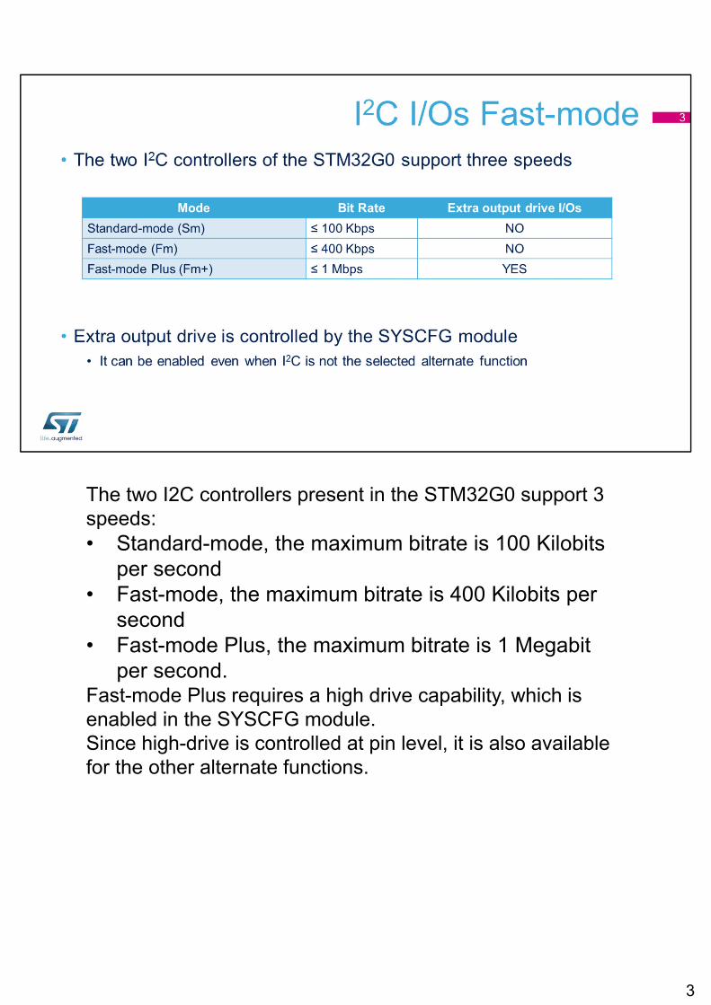
The two I2C controllers present in the STM32G0 support 3 speeds:• Standard-mode, the maximum bitrate is 100 Kilobits
per second• Fast-mode, the maximum bitrate is 400 Kilobits per
second• Fast-mode Plus, the maximum bitrate is 1 Megabit
per second.Fast-mode Plus requires a high drive capability, which isenabled in the SYSCFG module.Since high-drive is controlled at pin level, it is also availablefor the other alternate functions.
3

The high-drive capability of the I2C1 pins can be configured per pin through the I2C_PA9-10_FMP and I2C_PB6-9_FMP bits or globally by setting the I2C1_FMP bit.The high-drive capability of the I2C2 pins is controlled globally by setting the I2C2_FMP bit.
4
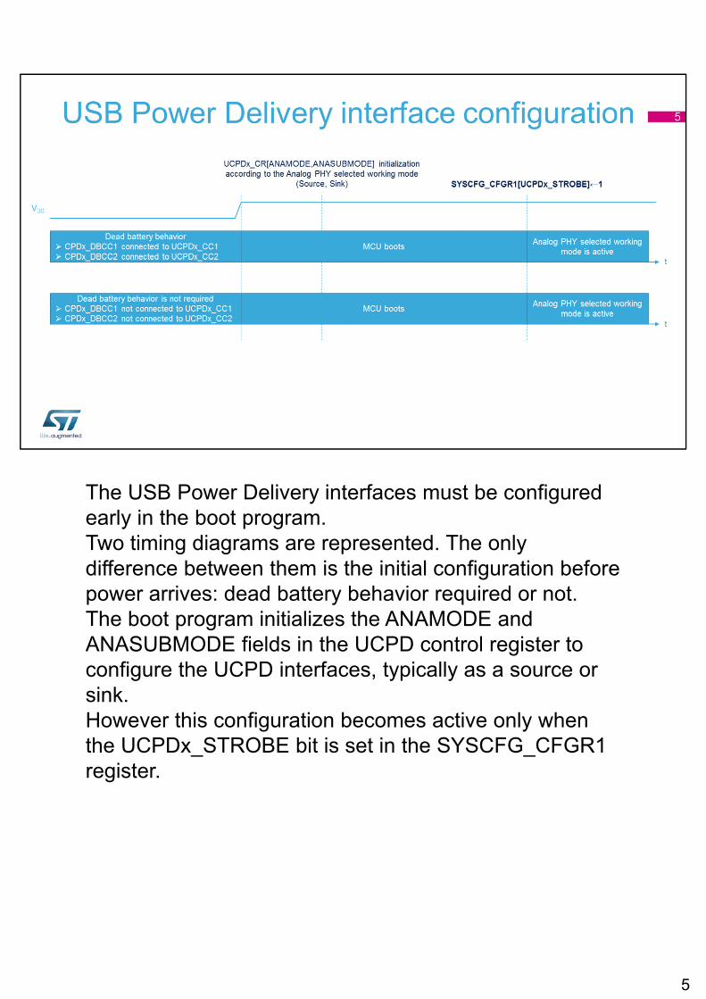
The USB Power Delivery interfaces must be configured early in the boot program.Two timing diagrams are represented. The only difference between them is the initial configuration before power arrives: dead battery behavior required or not. The boot program initializes the ANAMODE and ANASUBMODE fields in the UCPD control register to configure the UCPD interfaces, typically as a source or sink.However this configuration becomes active only when the UCPDx_STROBE bit is set in the SYSCFG_CFGR1 register.
5

The STM32G0 supports a voltage booster that should beused when the analog inputs operate in low VDD voltage.It is activated by setting the BOOSTEN bit in the SYSCFG_CFGR1 register.
6

The Infrared Timer (IRTIM) unit requires a modulation envelope signal that is provided either by USARTs or by TIM16. The IR_MOD field in SYSCFG_CFGR1 register controls the related input multiplexer. The IR_POL bit in the SYSCFG_CFGR1 register selects whether or not the output signal is inverted.
7

When the PA11_PA12_RMP bit in the SYSCFG_CFGR1 register is set, the PA11 and PA12 alternate functions are remapped to pins PA9 and PA10.This is useful when these alternate functions are needed while the PA11 and PA12 pins are not available in low pin-count packages.
8

The MEM_MODE field in the SYSCFG_CFGR1 register selects which memory is accessible at address 0.Three memories can be aliased to address 0: Main Flash memory, System Flash memory or SRAM.Note that the default setting of this field depends on boot pin, option bytes and control bit.
9
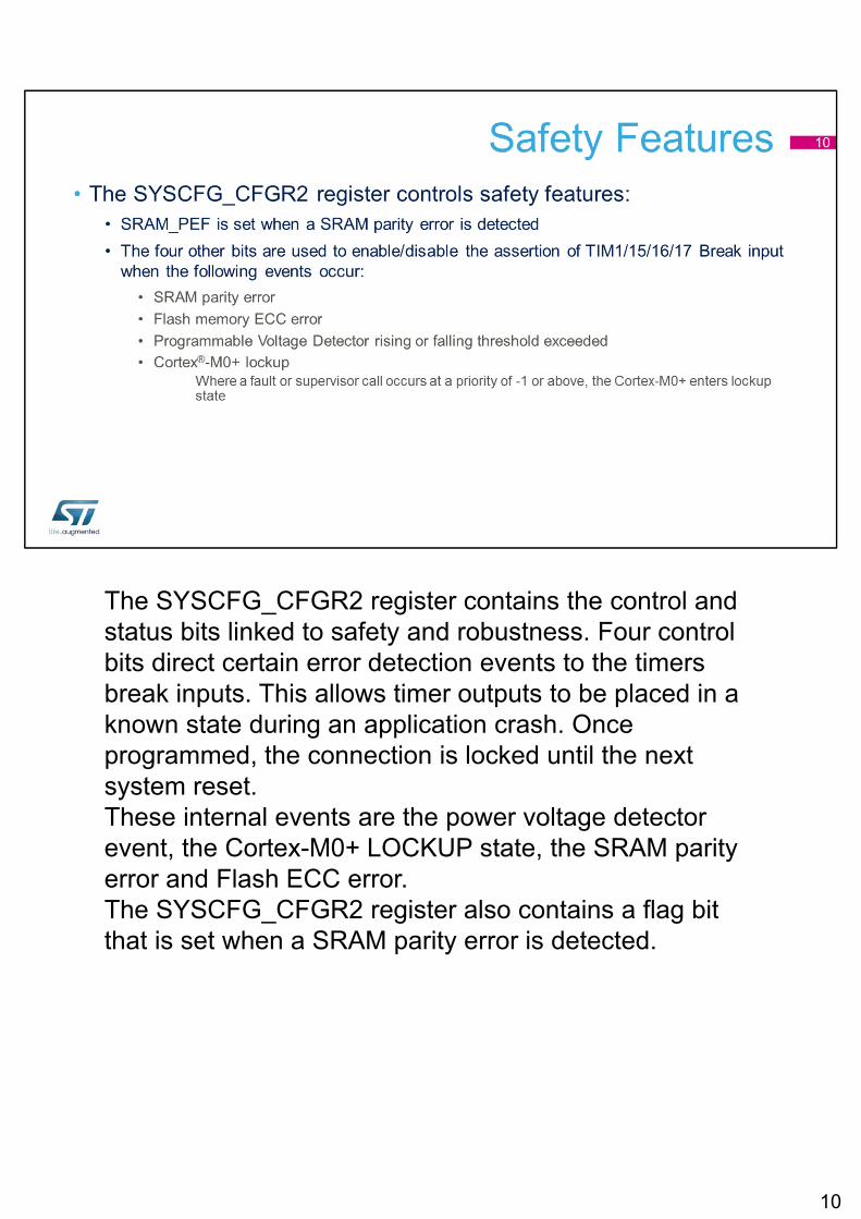
The SYSCFG_CFGR2 register contains the control and status bits linked to safety and robustness. Four control bits direct certain error detection events to the timers break inputs. This allows timer outputs to be placed in a known state during an application crash. Once programmed, the connection is locked until the next system reset. These internal events are the power voltage detector event, the Cortex-M0+ LOCKUP state, the SRAM parity error and Flash ECC error.The SYSCFG_CFGR2 register also contains a flag bit that is set when a SRAM parity error is detected.
10

The SYSCFG module supports 32 interrupt line statusregisters.They enable software to easily find the cause of an EXTI interrupt, by collecting in the same register all pending interrupt sources associated with a particular interrupt line.In order to explain the benefit of these interrupt line statusregisters, the following slide will focus on the EXTI2 and EXTI3 interrupt lines.
11

The left part of the figure represents the peripherals able to assert EXTI2 and EXTI3, respectively RTC/TAMPER and Flash memory units.Regarding EXTI2, RTC and Tamper interrupt requests are ORed together.Regarding EXTI3, Flash memory ECC and Flash interface interrupt requests are ORed together.Furthermore EXTI2 and EXTI3 interrupt requests are also ORed together to generate the INT number 5 received by the Cortex®-M0+ NVIC.In the INT5 interrupt service routine, software should first read the SYSCFG_ITLINE6 register to determine whether EXTI2 or EXTI3 is pending and then either SYSCFG_ITLINE2 or SYSCFG_ITLINE3 register to determine the exact cause of the interrupt.
12

In addition to this training, you can refer to I2C, UCPD, IRTIM, GPIO, Flash memory, interrupts and timers trainings.
13
For more details, please refer to application note AN2606: STM32 microcontroller system memory boot mode.
14