Embed Size (px)
DESCRIPTION
Stm32f4 Hardware Development
Citation preview

October 2014 DocID026304 Rev 2 1/43
AN4488Application note
Getting started with STM32F4xxxx MCU hardware development
Introduction
This application note is intended for system designers who require an overview of the hardware implementation of the development board, with focus on features like
• power supply
• package selection
• clock management
• reset control
• boot mode settings
• debug management.
This document shows how to use the high-density high-performance microcontrollers listed in Table 1, and describes the minimum hardware resources required to develop an application based on those products.
Detailed reference design schematics are also contained in this document, together with descriptions of the main components, interfaces and modes.
Table 1. Applicable products
Type Part Number
Microcontrollers
STM32F401xB / STM32F401xC
STM32F401xD / STM32F401xE
STM32F405xx / STM32F407xx
STM32F411xC / STM32F411xE
STM32F415xx / STM32F417xx
STM32F427xx / STM32F429xx
STM32F437xx / STM32F439xx
www.st.com

Contents AN4488
2/43 DocID026304 Rev 2
Contents
1 Reference documents . . . . . . . . . . . . . . . . . . . . . . . . . . . . . . . . . . . . . . . . 6
2 Power supplies . . . . . . . . . . . . . . . . . . . . . . . . . . . . . . . . . . . . . . . . . . . . . 7
2.1 Introduction . . . . . . . . . . . . . . . . . . . . . . . . . . . . . . . . . . . . . . . . . . . . . . . . 7
2.1.1 Independent A/D converter supply and reference voltage . . . . . . . . . . . . 7
2.1.2 Battery backup . . . . . . . . . . . . . . . . . . . . . . . . . . . . . . . . . . . . . . . . . . . . . 7
2.1.3 Voltage regulator . . . . . . . . . . . . . . . . . . . . . . . . . . . . . . . . . . . . . . . . . . . 8
2.2 Power supply schemes . . . . . . . . . . . . . . . . . . . . . . . . . . . . . . . . . . . . . . . 8
2.3 Reset & power supply supervisor . . . . . . . . . . . . . . . . . . . . . . . . . . . . . . . 10
2.3.1 Power on reset (POR) / power down reset (PDR) . . . . . . . . . . . . . . . . . 10
2.3.2 Programmable voltage detector (PVD) . . . . . . . . . . . . . . . . . . . . . . . . . 10
2.3.3 System reset . . . . . . . . . . . . . . . . . . . . . . . . . . . . . . . . . . . . . . . . . . . . . 11
2.3.4 PDR_ON circuitry example . . . . . . . . . . . . . . . . . . . . . . . . . . . . . . . . . . 12
2.3.5 NRST circuitry example (for STM32F411xx only) . . . . . . . . . . . . . . . . . 14
2.3.6 Regulator OFF mode . . . . . . . . . . . . . . . . . . . . . . . . . . . . . . . . . . . . . . . 16
2.3.7 Regulator ON/OFF and internal reset ON/OFF availability . . . . . . . . . . 17
3 Package . . . . . . . . . . . . . . . . . . . . . . . . . . . . . . . . . . . . . . . . . . . . . . . . . . 18
3.1 Package Selection . . . . . . . . . . . . . . . . . . . . . . . . . . . . . . . . . . . . . . . . . . 18
3.2 Pinout Compatibility . . . . . . . . . . . . . . . . . . . . . . . . . . . . . . . . . . . . . . . . . 20
3.2.1 Compatibility within STM32F4x family . . . . . . . . . . . . . . . . . . . . . . . . . . 21
3.2.2 Compatibility with STM32F1x and STM32F2x families . . . . . . . . . . . . . 22
3.3 Alternate Function mapping to pins . . . . . . . . . . . . . . . . . . . . . . . . . . . . . 24
4 Clocks . . . . . . . . . . . . . . . . . . . . . . . . . . . . . . . . . . . . . . . . . . . . . . . . . . . . 25
4.1 HSE OSC clock . . . . . . . . . . . . . . . . . . . . . . . . . . . . . . . . . . . . . . . . . . . . 25
4.1.1 External source (HSE bypass) . . . . . . . . . . . . . . . . . . . . . . . . . . . . . . . . 26
4.1.2 External crystal/ceramic resonator (HSE crystal) . . . . . . . . . . . . . . . . . 26
4.2 LSE OSC clock . . . . . . . . . . . . . . . . . . . . . . . . . . . . . . . . . . . . . . . . . . . . . 27
4.2.1 External source (LSE bypass) . . . . . . . . . . . . . . . . . . . . . . . . . . . . . . . . 27
4.2.2 External crystal/ceramic resonator (LSE crystal) . . . . . . . . . . . . . . . . . . 27
4.3 Clock security system (CSS) . . . . . . . . . . . . . . . . . . . . . . . . . . . . . . . . . . 28
5 Boot configuration . . . . . . . . . . . . . . . . . . . . . . . . . . . . . . . . . . . . . . . . . 29

DocID026304 Rev 2 3/43
AN4488 Contents
3
5.1 Boot mode selection . . . . . . . . . . . . . . . . . . . . . . . . . . . . . . . . . . . . . . . . . 29
5.2 Boot pin connection . . . . . . . . . . . . . . . . . . . . . . . . . . . . . . . . . . . . . . . . . 29
5.3 Embedded boot loader mode . . . . . . . . . . . . . . . . . . . . . . . . . . . . . . . . . . 30
6 Debug management . . . . . . . . . . . . . . . . . . . . . . . . . . . . . . . . . . . . . . . . 31
6.1 Introduction . . . . . . . . . . . . . . . . . . . . . . . . . . . . . . . . . . . . . . . . . . . . . . . 31
6.2 SWJ debug port (serial wire and JTAG) . . . . . . . . . . . . . . . . . . . . . . . . . . 31
6.3 Pinout and debug port pins . . . . . . . . . . . . . . . . . . . . . . . . . . . . . . . . . . . 31
6.3.1 SWJ debug port pins . . . . . . . . . . . . . . . . . . . . . . . . . . . . . . . . . . . . . . . 31
6.3.2 Flexible SWJ-DP pin assignment . . . . . . . . . . . . . . . . . . . . . . . . . . . . . 32
6.3.3 Internal pull-up and pull-down resistors on JTAG pins . . . . . . . . . . . . . . 32
6.3.4 SWJ debug port connection with standard JTAG connector . . . . . . . . . 33
7 Recommendations . . . . . . . . . . . . . . . . . . . . . . . . . . . . . . . . . . . . . . . . . 34
7.1 Printed circuit board . . . . . . . . . . . . . . . . . . . . . . . . . . . . . . . . . . . . . . . . . 34
7.2 Component position . . . . . . . . . . . . . . . . . . . . . . . . . . . . . . . . . . . . . . . . . 34
7.3 Ground and power supply (VSS, VDD) . . . . . . . . . . . . . . . . . . . . . . . . . . . 34
7.4 Decoupling . . . . . . . . . . . . . . . . . . . . . . . . . . . . . . . . . . . . . . . . . . . . . . . . 34
7.5 Other signals . . . . . . . . . . . . . . . . . . . . . . . . . . . . . . . . . . . . . . . . . . . . . . 35
7.6 Unused I/Os and features . . . . . . . . . . . . . . . . . . . . . . . . . . . . . . . . . . . . 35
8 Reference design . . . . . . . . . . . . . . . . . . . . . . . . . . . . . . . . . . . . . . . . . . 36
8.1 Description . . . . . . . . . . . . . . . . . . . . . . . . . . . . . . . . . . . . . . . . . . . . . . . . 36
8.1.1 Clock . . . . . . . . . . . . . . . . . . . . . . . . . . . . . . . . . . . . . . . . . . . . . . . . . . . 36
8.1.2 Reset . . . . . . . . . . . . . . . . . . . . . . . . . . . . . . . . . . . . . . . . . . . . . . . . . . . 36
8.1.3 Boot mode . . . . . . . . . . . . . . . . . . . . . . . . . . . . . . . . . . . . . . . . . . . . . . . 36
8.1.4 SWJ interface . . . . . . . . . . . . . . . . . . . . . . . . . . . . . . . . . . . . . . . . . . . . 36
8.1.5 Power supply . . . . . . . . . . . . . . . . . . . . . . . . . . . . . . . . . . . . . . . . . . . . . 36
8.2 Component references . . . . . . . . . . . . . . . . . . . . . . . . . . . . . . . . . . . . . . . 37
9 Revision history . . . . . . . . . . . . . . . . . . . . . . . . . . . . . . . . . . . . . . . . . . . 42

List of tables AN4488
4/43 DocID026304 Rev 2
List of tables
Table 1. Applicable products . . . . . . . . . . . . . . . . . . . . . . . . . . . . . . . . . . . . . . . . . . . . . . . . . . . . . . . 1Table 2. Referenced documents. . . . . . . . . . . . . . . . . . . . . . . . . . . . . . . . . . . . . . . . . . . . . . . . . . . . . 6Table 3. Regulator ON/OFF and internal power supply supervisor availability. . . . . . . . . . . . . . . . . 17Table 4. Package summary (Excluding WCSP) . . . . . . . . . . . . . . . . . . . . . . . . . . . . . . . . . . . . . . . . 18Table 5. WCSP Package summary . . . . . . . . . . . . . . . . . . . . . . . . . . . . . . . . . . . . . . . . . . . . . . . . . 19Table 6. Pinout summary . . . . . . . . . . . . . . . . . . . . . . . . . . . . . . . . . . . . . . . . . . . . . . . . . . . . . . . . . 20Table 7. Boot modes. . . . . . . . . . . . . . . . . . . . . . . . . . . . . . . . . . . . . . . . . . . . . . . . . . . . . . . . . . . . . 29Table 8. Debug port pin assignment . . . . . . . . . . . . . . . . . . . . . . . . . . . . . . . . . . . . . . . . . . . . . . . . . 32Table 9. SWJ I/O pin availability . . . . . . . . . . . . . . . . . . . . . . . . . . . . . . . . . . . . . . . . . . . . . . . . . . . . 32Table 10. Mandatory components . . . . . . . . . . . . . . . . . . . . . . . . . . . . . . . . . . . . . . . . . . . . . . . . . . . 37Table 11. Optional components . . . . . . . . . . . . . . . . . . . . . . . . . . . . . . . . . . . . . . . . . . . . . . . . . . . . . 37Table 12. Reference connection for all packages. . . . . . . . . . . . . . . . . . . . . . . . . . . . . . . . . . . . . . . . 39Table 13. Document revision history . . . . . . . . . . . . . . . . . . . . . . . . . . . . . . . . . . . . . . . . . . . . . . . . . 42
DocID026304 Rev 2 5/43
AN4488 List of figures
5
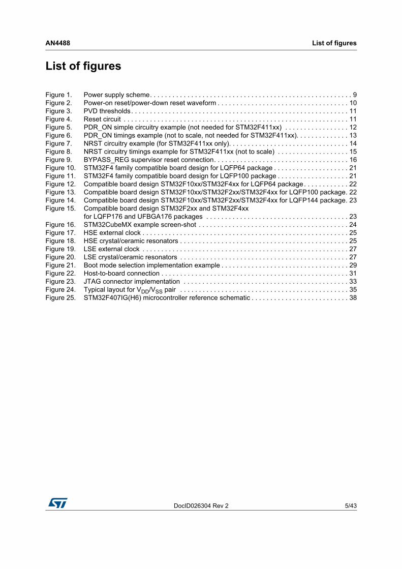
List of figures
Figure 1. Power supply scheme. . . . . . . . . . . . . . . . . . . . . . . . . . . . . . . . . . . . . . . . . . . . . . . . . . . . . . 9Figure 2. Power-on reset/power-down reset waveform . . . . . . . . . . . . . . . . . . . . . . . . . . . . . . . . . . . 10Figure 3. PVD thresholds. . . . . . . . . . . . . . . . . . . . . . . . . . . . . . . . . . . . . . . . . . . . . . . . . . . . . . . . . . 11Figure 4. Reset circuit . . . . . . . . . . . . . . . . . . . . . . . . . . . . . . . . . . . . . . . . . . . . . . . . . . . . . . . . . . . . 11Figure 5. PDR_ON simple circuitry example (not needed for STM32F411xx) . . . . . . . . . . . . . . . . . 12Figure 6. PDR_ON timings example (not to scale, not needed for STM32F411xx). . . . . . . . . . . . . . 13Figure 7. NRST circuitry example (for STM32F411xx only). . . . . . . . . . . . . . . . . . . . . . . . . . . . . . . . 14Figure 8. NRST circuitry timings example for STM32F411xx (not to scale) . . . . . . . . . . . . . . . . . . . 15Figure 9. BYPASS_REG supervisor reset connection. . . . . . . . . . . . . . . . . . . . . . . . . . . . . . . . . . . . 16Figure 10. STM32F4 family compatible board design for LQFP64 package . . . . . . . . . . . . . . . . . . . . 21Figure 11. STM32F4 family compatible board design for LQFP100 package . . . . . . . . . . . . . . . . . . . 21Figure 12. Compatible board design STM32F10xx/STM32F4xx for LQFP64 package. . . . . . . . . . . . 22Figure 13. Compatible board design STM32F10xx/STM32F2xx/STM32F4xx for LQFP100 package. 22Figure 14. Compatible board design STM32F10xx/STM32F2xx/STM32F4xx for LQFP144 package. 23Figure 15. Compatible board design STM32F2xx and STM32F4xx
for LQFP176 and UFBGA176 packages . . . . . . . . . . . . . . . . . . . . . . . . . . . . . . . . . . . . . . 23Figure 16. STM32CubeMX example screen-shot . . . . . . . . . . . . . . . . . . . . . . . . . . . . . . . . . . . . . . . . 24Figure 17. HSE external clock . . . . . . . . . . . . . . . . . . . . . . . . . . . . . . . . . . . . . . . . . . . . . . . . . . . . . . . 25Figure 18. HSE crystal/ceramic resonators . . . . . . . . . . . . . . . . . . . . . . . . . . . . . . . . . . . . . . . . . . . . . 25Figure 19. LSE external clock . . . . . . . . . . . . . . . . . . . . . . . . . . . . . . . . . . . . . . . . . . . . . . . . . . . . . . . 27Figure 20. LSE crystal/ceramic resonators . . . . . . . . . . . . . . . . . . . . . . . . . . . . . . . . . . . . . . . . . . . . . 27Figure 21. Boot mode selection implementation example . . . . . . . . . . . . . . . . . . . . . . . . . . . . . . . . . . 29Figure 22. Host-to-board connection . . . . . . . . . . . . . . . . . . . . . . . . . . . . . . . . . . . . . . . . . . . . . . . . . . 31Figure 23. JTAG connector implementation . . . . . . . . . . . . . . . . . . . . . . . . . . . . . . . . . . . . . . . . . . . . 33Figure 24. Typical layout for VDD/VSS pair . . . . . . . . . . . . . . . . . . . . . . . . . . . . . . . . . . . . . . . . . . . . . 35Figure 25. STM32F407IG(H6) microcontroller reference schematic . . . . . . . . . . . . . . . . . . . . . . . . . . 38

Reference documents AN4488
6/43 DocID026304 Rev 2
1 Reference documents
The following documents are available on www.st.com
Table 2. Referenced documents
Reference Title
AN2867 Oscillator design guide for ST microcontrollers
AN2606 STM32 microcontroller system memory boot mode
AN3364 Migration and compatibility guidelines for STM32 microcontroller applications

DocID026304 Rev 2 7/43
AN4488 Power supplies
42
2 Power supplies
2.1 Introduction
The operating voltage supply (VDD) range is 1.8 V to 3.6 V, which can be reduced down to 1.7 V with some restrictions, as detailed in the product datasheets. An embedded regulator is used to supply the internal 1.2 V digital power.
The real-time clock (RTC) and backup registers can be powered from the VBAT voltage when the main VDD supply is powered off.
2.1.1 Independent A/D converter supply and reference voltage
To improve conversion accuracy, the ADC has an independent power supply that can be filtered separately, and shielded from noise on the PCB.
• the ADC voltage supply input is available on a separate VDDA pin
• an isolated supply ground connection is provided on the VSSA pin In all cases, the VSSA pin should be externally connected to same supply ground than VSS
On packages with 100-pins and above
To ensure a better accuracy on low-voltage inputs, the user can connect a separate external reference voltage ADC input on VREF+. The voltage on VREF+ may range from (VDDA- 1.2 V) to VDDA with a minimum of 1.7 V.
When available (depending on package), VREF– must be externally tied to VSSA.
On packages with less than 100-pins
The VREF+ and VREF- pins are not available, they are internally connected to the ADC voltage supply (VDDA) and ground (VSSA).
2.1.2 Battery backup
To retain the content of the Backup registers when VDD is turned off, the VBAT pin can be connected to an optional standby voltage supplied by a battery or another source.
The VBAT pin also powers the RTC unit, allowing the RTC to operate even when the main digital supply (VDD) is turned off. The switch to the VBAT supply is controlled by the power down reset (PDR) circuitry embedded in the Reset block.
If no external battery is used in the application, it is highly recommended to connect VBAT externally to VDD.

Power supplies AN4488
8/43 DocID026304 Rev 2
2.1.3 Voltage regulator
The voltage regulator is always enabled after reset. It works in three different modes depending on the application modes.
• in Run mode, the regulator supplies full power to the 1.2 V domain (core, memories and digital peripherals)
• in Stop mode, the regulator supplies low power to the 1.2 V domain, preserving the contents of the registers and SRAM
• in Standby mode, the regulator is powered down. The contents of the registers and SRAM are lost except for those concerned with the Standby circuitry and the Backup domain.
Note: Depending on the selected package, there are specific pins that should be connected either to VSS or VDD to activate or deactivate the voltage regulator. Refer to section “Voltage regulator “ in datasheet for details.
2.2 Power supply schemes
The circuit is powered by a stabilized power supply, VDD.
Caution: The VDD voltage range is 1.8 V to 3.6 V (down to 1.7 V with some restrictions, see relative DataSheets for details)
• The VDD pins must be connected to VDD with external decoupling capacitors: one single Tantalum or Ceramic capacitor (min. 4.7 µF typ.10 µF) for the package + one 100 nF Ceramic capacitor for each VDD pin.
• The VBAT pin can be connected to the external battery (1.65 V < VBAT < 3.6 V). If no external battery is used, it is recommended to connect this pin to VDD with a 100 nF external ceramic decoupling capacitor.
• The VDDA pin must be connected to two external decoupling capacitors (100 nF Ceramic + 1 µF Tantalum or Ceramic).
• The VREF+ pin can be connected to the VDDA external power supply. If a separate, external reference voltage is applied on VREF+, a 100 nF and a 1 µF capacitors must be connected on this pin. In all cases, VREF+ must be kept between (VDDA-1.2 V) and VDDA with minimum of 1.7 V.
• must be kept between 1.65 V and VDDA.
• Additional precautions can be taken to filter analog noise:
– VDDA can be connected to VDD through a ferrite bead.
– The VREF+ pin can be connected to VDDA through a resistor (typ. 47 Ω).
• For the voltage regulator configuration, there is specific BYPASS_REG pin (not available on all packages) that should be connected either to VSS or VDD to activate or deactivate the voltage regulator specific.
– Refer to Section 2.3.6 and section "Voltage regulator" of the related device datasheet for details.
• When the voltage regulator is enabled, VCAP1 and VCAP2 pins must be connected to 2*2.2 µF LowESR < 2Ω Ceramic capacitor (or 1*4.7 µF LowESR < 1Ω Ceramic capacitor if only VCAP1 pin is provided on some packages).

DocID026304 Rev 2 9/43
AN4488 Power supplies
42
Figure 1. Power supply scheme
1. Optional. If a separate, external reference voltage is connected on VREF+, the two capacitors (100 nF and 1 µF) must be connected.
2. VCAP2 is not available on all packages. In that case, a single 4.7 µF (ESR < 1Ω) is connected to VCAP1
3. VREF+ is either connected to VREF+ or to VDDA (depending on package).
4. VREF- is either connected to VREF- or to VSSA (depending on package).
5. N is the number of VDD and VSS inputs.
6. Refer to section “Voltage regulator” in datasheet (Table 1) to connect BYPASS_REG and PDR_ON pins.

Power supplies AN4488
10/43 DocID026304 Rev 2
2.3 Reset & power supply supervisor
2.3.1 Power on reset (POR) / power down reset (PDR)
The device has an integrated POR/PDR circuitry that allows proper operation starting from 1.8 V.
The device remains in the Reset mode as long as VDD is below a specified threshold, VPOR/PDR, without the need for an external reset circuit. For more details concerning the power on/power down reset threshold, refer to the electrical characteristics in the product datasheets.
Figure 2. Power-on reset/power-down reset waveform
1. tRSTTEMPO is approximately 2.6 ms. VPOR/PDR rising edge is 1.74 V (typ.) and VPOR/PDR falling edge is 1.70 V (typ.). Refer to STM32F4xxxx datasheets for actual value.
The internal power-on reset (POR) / power-down reset (PDR) circuitry is disabled through the PDR_ON pin. An external power supply supervisor should monitor VDD and should maintain the device in reset mode as long as VDD is below a specified threshold. PDR_ON should be connected to this external power supply supervisor. See Section 2.3.4 and Section 2.3.5 for details.
2.3.2 Programmable voltage detector (PVD)
You can use the PVD to monitor the VDD power supply by comparing it to a threshold selected by the PLS[2:0] bits in the Power control register (PWR_CR).
The PVD is enabled by setting the PVDE bit.
A PVDO flag is available, in the Power control/status register (PWR_CSR), to indicate whether VDD is higher or lower than the PVD threshold. This event is internally connected to EXTI Line16 and can generate an interrupt if enabled through the EXTI registers. The PVD output interrupt can be generated when VDD drops below the PVD threshold and/or when VDD rises above the PVD threshold depending on the EXTI Line16 rising/falling edge configuration. As an example the service routine can perform emergency shutdown tasks.

DocID026304 Rev 2 11/43
AN4488 Power supplies
42
Figure 3. PVD thresholds
2.3.3 System reset
A system reset sets all registers to their reset values except for the reset flags in the clock controller CSR register and the registers in the Backup domain (see Figure 1).
A system reset is generated when one of the following events occurs:
1. A low level on the NRST pin (external reset)
2. window watchdog end-of-count condition (WWDG reset)
3. Independent watchdog end-of-count condition (IWDG reset)
4. A software reset (SW reset)
5. Low-power management reset
The reset source can be identified by checking the reset flags in the Control/Status register, RCC_CSR.
The products listed in Table 1 do not require an external reset circuit to power-up correctly. Only a pull-down capacitor is recommended to improve EMS performance by protecting the device against parasitic resets, as exemplified in Figure 4.
Charging and discharging a pull-down capacitor through an internal resistor increases the device power consumption. The capacitor recommended value (100 nF) can be reduced to 10 nF to limit this power consumption.
Figure 4. Reset circuit

Power supplies AN4488
12/43 DocID026304 Rev 2
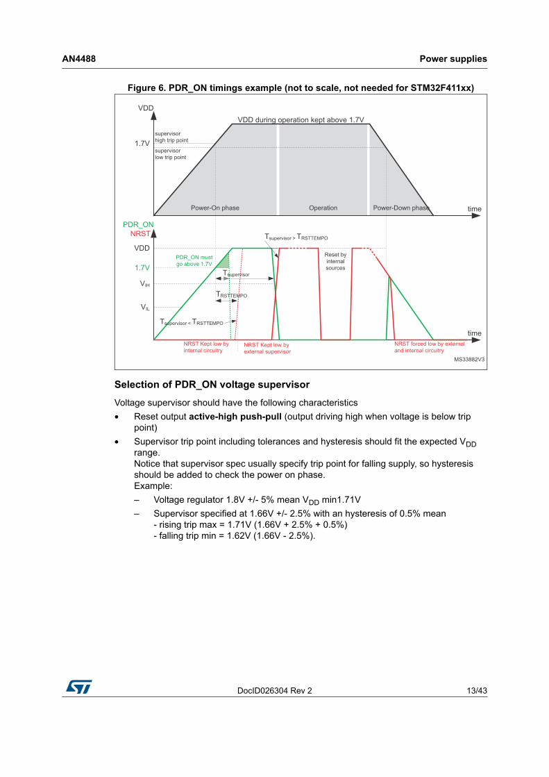
2.3.4 PDR_ON circuitry example
Note: This example doesn’t apply to STM32F411xx, where PDR_ON can be connected to VSS to permanently disable internal reset circuitry (external voltage supervisor required on NRST pin). Anyway (thanks to backward compatibility), circuitry built for other STM32F4xxxx products will work for STM32F411xx.
Note: Please contact your local STMicroelectronics representative or visit www.st.com in case you want to use circuitry different from the one described hereafter.
Restrictions:
• PDR_ON = 0 is mostly intended for VDD supply between 1.7 V and 1.9V (i.e. 1.8V +/- 5% supply). Supply ranges which never go below 1.8V minimum should be better managed with internal circuitry (no additional component thanks to fully embedded reset controller).
• To ensure safe power down, the external voltage supervisor (or equivalent) is required to drive PDR_ON=1 during power off sequence.
When the internal reset is OFF, the following integrated features are no longer supported:
• The integrated power-on reset (POR) / power-down reset (PDR) circuitry is disabled.
• The brownout reset (BOR) circuitry must be disabled.
• The embedded programmable voltage detector (PVD) is disabled.
• VBAT functionality is no more available and VBAT pin should be connected to VDD.
Figure 5. PDR_ON simple circuitry example (not needed for STM32F411xx)
DocID026304 Rev 2 13/43
AN4488 Power supplies
42
Figure 6. PDR_ON timings example (not to scale, not needed for STM32F411xx)
Selection of PDR_ON voltage supervisor
Voltage supervisor should have the following characteristics
• Reset output active-high push-pull (output driving high when voltage is below trip point)
• Supervisor trip point including tolerances and hysteresis should fit the expected VDD range. Notice that supervisor spec usually specify trip point for falling supply, so hysteresis should be added to check the power on phase. Example:
– Voltage regulator 1.8V +/- 5% mean VDD min1.71V
– Supervisor specified at 1.66V +/- 2.5% with an hysteresis of 0.5% mean - rising trip max = 1.71V (1.66V + 2.5% + 0.5%) - falling trip min = 1.62V (1.66V - 2.5%).

Power supplies AN4488
14/43 DocID026304 Rev 2
2.3.5 NRST circuitry example (for STM32F411xx only)
This example applies to STM32F411xx where PDR_ON can be connected to VSS to permanently disable internal reset circuitry.
Restrictions:
• PDR_ON = 0 is mostly intended for VDD supply between 1.7 V and 1.9V (i.e. 1.8V +/-5% supply). Supply ranges which never go below 1.8V minimum should be better managed by internal circuitry (no additional component needed, thanks to fully embedded reset controller).
• When the internal reset is OFF, the following integrated features are no longer supported:
– The integrated power-on reset (POR) / power-down reset (PDR) circuitry is disabled.
– The brownout reset (BOR) circuitry must be disabled.
– The embedded programmable voltage detector (PVD) is disabled.
– VBAT functionality is no more available and VBAT pin should be connected to VDD.
Figure 7. NRST circuitry example (for STM32F411xx only)
Even with PDR_ON=0, during power up, the NRST is driven low by internal Reset controller
during TRSTTEMPO in order to allow stabilization of internal analog circuitry. Refer to
STM32F4xxxx datasheets for actual timing value.

DocID026304 Rev 2 15/43
AN4488 Power supplies
42
Figure 8. NRST circuitry timings example for STM32F411xx (not to scale)
Selection of NRST voltage supervisor
Voltage supervisor should have the following characteristics
• Reset output active-low open-drain (output driving low when voltage is below trip point).
• Supervisor trip point including tolerances and hysteresis should fit the expected VDD range. Notice that supervisor spec usually specify trip point for falling supply, so hysteresis should be added to check the power on phase. Example for STM1061N16:
– Voltage regulator 1.8 V +/- 5% mean VDD min1.71 V
– Supervisor specified at 1.60 V +/- 2% with an hysteresis of 5% mean - rising trip max = 1.71 V (1.60 V + 2% + 5%) - falling trip min = 1.57 V (1.60 V - 2%).

Power supplies AN4488
16/43 DocID026304 Rev 2
2.3.6 Regulator OFF mode
Refer to section “Voltage regulator” in datasheet for details.
• When BYPASS_REG = VDD, the core power supply should be provided through VCAP1 and VCAP1 pins connected together.
– The two VCAP ceramic capacitors should be replaced by two 100 nF decoupling capacitors.
– Since the internal voltage scaling is not managed internally, the external voltage value must be aligned with the targeted maximum frequency.
– When the internal regulator is OFF, there is no more internal monitoring on V12. An external power supply supervisor should be used to monitor the V12 of the logic power domain (VCAP). PA0 pin should be used for this purpose, and act as power-on reset on V12 power domain.
• In regulator OFF mode, the following features are no more supported:
– PA0 cannot be used as a GPIO pin since it allows to reset a part of the V12 logic power domain which is not reset by the NRST pin.
– As long as PA0 is kept low, the debug mode cannot be used under power-on reset. As a consequence, PA0 and NRST pins must be managed separately if the debug connection under reset or pre-reset is required.
– The over-drive and under-drive modes are not available.
– The Standby mode is not available.
Figure 9. BYPASS_REG supervisor reset connection
1. VCAP2 is not available on all packages. In that case, a single 100 nF decoupling capacitor is connected to VCAP1

DocID026304 Rev 2 17/43
AN4488 Power supplies
42
The following conditions must be respected:
• VDD should always be higher than VCAP to avoid current injection between power domains.
• If the time for VCAP to reach V12 minimum value is smaller than the time for VDD to reach 1.7 V, then PA0 should be kept low to cover both conditions: until VCAP reaches V12 minimum value and until VDD reaches 1.7 V.
• Otherwise, if the time for VCAP to reach V12 minimum value is smaller than the time for VDD to reach 1.7 V, then PA0 could be asserted low externally.
• If VCAP goes below V12 minimum value and VDD is higher than 1.7 V, then PA0 must be asserted low externally.
2.3.7 Regulator ON/OFF and internal reset ON/OFF availability
Table 3. Regulator ON/OFF and internal power supply supervisor availability
Package pins Regulator ON Regulator OFFPower supply supervisor ON
Power supply supervisor OFF
Packages with pins on 4 edges
48
Yes(1) NoYes(2) No64
100
144
Yes
PDR_ON set to VDD
Yes
PDR_ON external control(3)
176 Yes(4) Yes(5)
208 Yes(1) No
BGA Packages
100
Yes(4) Yes(5)169
176
216
Chip Scale Packages
49 Yes(1) No
90 Yes(4) Yes(5)
143
1. BYPASS_REG internally connected to VSS
2. PDR_ON internally connected to VDD
3. PDR_ON can be permanently set to VSS for STM32F411xx devices. For other devices, see Chapter 2.3.4
4. BYPASS_REG set to VSS
5. BYPASS_REG set to VDD

Package AN4488
18/43 DocID026304 Rev 2
3 Package
3.1 Package Selection
Package should be selected by taking into account the constrains that are strongly dependent upon the application.
The list below summarizes the more frequent ones:
– Amount of interfaces required. Some interfaces might not be available on some packages. Some interfaces combinations could not be possible on some packages
– PCB technology constrains. Small pitch and high ball density could require more PCB layers and higher class PCB
– Package height
– PCB available area
– Noise emission or signal integrity of high speed interfaces. Smaller packages usually provide better signal integrity. This is further enhanced as Small pitch and high ball density requires multilayer PCBs which allow better supply/ground distribution.
– Compatibility with other devices.
Table 4. Package summary (Excluding WCSP)
Size (mm)(1) 7 x 7 10 x 10 14 x 14 7 x 7 20 x 20 24 x 24 7 x 7 10 x 10 28 x 28 13 x 13
Pitch (mm) 0.5 0.5 0.5 0.5 0.5 0.5 0.5 0.65 0.5 0.8
Height (mm) 0.6 1.6 1.6 0.6 1.6 1.6 0.6 0.6 1.6 1.1
Sales numbers
UF
QF
PN
48
LQ
FP
64
LQ
FP
100
UF
BG
A1
00
LQ
FP
144
LQ
FP
176
UF
BG
A1
69
UF
BG
A1
76+
25
LQ
FP
208
TF
BG
A21
6
STM32F405xx / 407xx / 415xx / 417xx
- X X - X X - X - -
STM32F42xxx / 43xxx - - X - X X X X X X
STM32F401xB/C X X X X - - - - - -
STM32F401xD/E X X X X - - - - - -
STM32F411xx X X X X - - - - - -
1. body size, excluding pins

DocID026304 Rev 2 19/43
AN4488 Package
42
Table 5. WCSP Package summary
Sales numbers Number of balls Size (mm) Pitch (mm) Height (mm)
STM32F405xx /407xx /415xx /417xx
90 4.258 x 4.004 0.4 0.62
STM32F42xxx / 43xxx 143 4.556 x 5.582 0.4 0.585
STM32F401xB/C 49(1) 3 x 3 0.4 0.585
STM32F401xD/E 49(1) 3.064 x 3.064 0.4 0.585
STM32F411xx 49(1) 3.034 x 3.22 0.4 0.585
1. Same ballout and ball pitch, only package overall dimension changes
Package AN4488
20/43 DocID026304 Rev 2
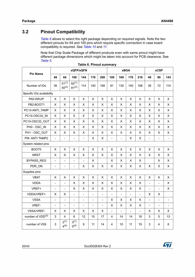
3.2 Pinout Compatibility
Table 6 allows to select the right package depending on required signals. Note the two different pinouts for 64 and 100 pins which require specific connection in case board compatibility is required. See Table 10 and 11.
Note that Chip Scale Package of different products even with same pinout might have different package dimensions which might be taken into account for PCB clearance. See Table 5.
Table 6. Pinout summary
Pin NamexQFP/xQFN xBGA xCSP
48 64 100 144 176 208 100 169 176 216 49 90 143
Number of IOs 3651(1)
50(2)82(1)
81(2) 114 140 168 81 130 140 168 36 72 114
Specific IOs availability
PA0-WKUP X X X X X X X X X X X X X
PB2-BOOT1 X X X X X X X X X X X X X
PC13-ANTI_TAMP X X X X X X X X X X X X X
PC14-OSC32_IN X X X X X X X X X X X X X
PC15-OSC32_OUT X X X X X X X X X X X X X
PH0 - OSC_IN X X X X X X X X X X X X X
PH1 - OSC_OUT X X X X X X X X X X X X X
PI8- ANTI TAMP2 - - - - X X - - X X - - -
System related pins
BOOT0 X X X X X X X X X X X X X
NRST X X X X X X X X X X X X X
BYPASS_REG - - - - X X X X X X X
PDR_ON - - - X X X X X X X X X X
Supplies pins
VBAT X X X X X X X X X X X X X
VDDA - - X X X X X X X X - - X
VREF+ - - X X X X X X X X - - X
VDDA/VREF+ X X - - - - - - - - X X
VSSA - - - - - - X X X X - - -
VREF- - - - - - - X X X X - - -
VSSA/VREF- X X X X X X - - - - X X X
number of VDD(3) 3 4 6 12 15 17 4 14 14 18 3 5 13
number of VSS 32(1)
4(4)3(1)
5(4) 9 11 14 4 10 11 19 3 4 6

DocID026304 Rev 2 21/43
AN4488 Package
42
3.2.1 Compatibility within STM32F4x family
Figure 10. STM32F4 family compatible board design for LQFP64 package
Figure 11. STM32F4 family compatible board design for LQFP100 package
VCAP1 X X X X X X X - X - X X X
VCAP2 - X(4) X X X X X - X - - X X
1. Apply to STM32F405xx / F407xx / F415xx / F417xxx / F427xx / F429xx / F437xx / F439xx
2. PB11 isn’t present on STM32F401xx / F411xx for 64 and 100 pins xQFP/xQFN packages
3. One single Tantalum or Ceramic capacitor (min. 4.7 µF typ.10 µF) for the package + one 100 nF Ceramic capacitor for each VDD pin
4. Apply to STM32F401xx / F411xx
Table 6. Pinout summary (continued)
Pin NamexQFP/xQFN xBGA xCSP
48 64 100 144 176 208 100 169 176 216 49 90 143

Package AN4488
22/43 DocID026304 Rev 2
3.2.2 Compatibility with STM32F1x and STM32F2x families
Figure 12. Compatible board design STM32F10xx/STM32F4xx for LQFP64 package
Figure 13. Compatible board design STM32F10xx/STM32F2xx/STM32F4xx for LQFP100 package

DocID026304 Rev 2 23/43
AN4488 Package
42
Figure 14. Compatible board design STM32F10xx/STM32F2xx/STM32F4xx for LQFP144 package
Figure 15. Compatible board design STM32F2xx and STM32F4xx for LQFP176 and UFBGA176 packages

Package AN4488
24/43 DocID026304 Rev 2
3.3 Alternate Function mapping to pins
In order to easily explore Peripheral Alternate Functions mapping to pins, it is recommended to use the STM32CubeMX tool available on www.st.com.
Figure 16. STM32CubeMX example screen-shot

DocID026304 Rev 2 25/43
AN4488 Clocks
42
4 Clocks
Three different clock sources can be used to drive the system clock (SYSCLK):
• HSI oscillator clock (high-speed internal clock signal)
• HSE oscillator clock (high-speed external clock signal)
• PLL clock
The devices have two secondary clock sources:
• 32 kHz low-speed internal RC (LSI RC) that drives the independent watchdog and, optionally, the RTC used for Auto-wakeup from the Stop/Standby modes.
• 32.768 kHz low-speed external crystal (LSE crystal) that optionally drives the real-time clock (RTCCLK)
Each clock source can be switched on or off independently when it is not used, to optimize the power consumption.
Refer to the reference manual for the description of the clock tree.
4.1 HSE OSC clock
The high-speed external clock signal (HSE) can be generated from two possible clock sources:
• HSE user external clock (see Figure 17)
• HSE external crystal/ceramic resonator (see Figure 18)
1. The value of REXT depends on the crystal characteristics. Typical value is in the range of 5 to 6 RS (resonator series resistance).
2. Load capacitance CL has the following formula: CL = CL1 x CL2 / (CL1 + CL2) + Cstray where: Cstray is the pin capacitance and board or trace PCB-related capacitance. Typically, it is between 2 pF and 7 pF. Please refer to Section 7: Recommendations on page 34 to minimize its value.
Figure 17. HSE external clock Figure 18. HSE crystal/ceramic resonators

Clocks AN4488
26/43 DocID026304 Rev 2
4.1.1 External source (HSE bypass)
In this mode, an external clock source must be provided. It can have a frequency from 1 to 50 MHz (refer to STM32F4xxxx datasheets for actual max value).
The external clock signal (square, sine or triangle) with a duty cycle of about 50%, has to drive the OSC_IN pin while the OSC_OUT pin must be left in the high impedance state (see Figure 18 and Figure 17).
4.1.2 External crystal/ceramic resonator (HSE crystal)
The external oscillator frequency ranges from 4 to 26 MHz.
The external oscillator has the advantage of producing a very accurate rate on the main clock. The associated hardware configuration is shown in Figure 18. Using a 25 MHz oscillator frequency is a good choice to get accurate Ethernet, USB OTG high-speed peripheral, and I2S.
The resonator and the load capacitors have to be connected as close as possible to the oscillator pins in order to minimize output distortion and startup stabilization time. The load capacitance values must be adjusted according to the selected oscillator.
For CL1 and CL2 it is recommended to use high-quality ceramic capacitors in the 5 pF-to-25 pF range (typ.), designed for high-frequency applications and selected to meet the requirements of the crystal or resonator. CL1 and CL2, are usually the same value. The crystal manufacturer typically specifies a load capacitance that is the series combination of CL1 and CL2. The PCB and MCU pin capacitances must be included when sizing CL1 and CL2 (10 pF can be used as a rough estimate of the combined pin and board capacitance).
Refer to the dedicated Application Note (AN2867 - Oscillator design guide for ST microcontrollers) and electrical characteristics sections in the datasheet of your product for more details.

DocID026304 Rev 2 27/43
AN4488 Clocks
42
4.2 LSE OSC clock
The low-speed external clock signal (LSE) can be generated from two possible clock sources:
• LSE user external clock (see Figure 19)
• LSE external crystal/ceramic resonator (see Figure 20)
1. “LSE crystal/ceramic resonators” figure: To avoid exceeding the maximum value of CL1 and CL2 (15 pF) it is strongly recommended to use a resonator with a load capacitance CL ≤ 7 pF. Never use a resonator with a load capacitance of 12.5 pF.
2. “LSE external clock” and “LSE crystal/ceramic resonators” figures: OSC32_IN and OSC32_OUT pins can be used also as GPIO, but it is recommended not to use them as both RTC and GPIO pins in the same application.
3. “LSE crystal/ceramic resonators” figure: The value of REXT depends on the crystal characteristics. A 0 Ω resistor would work but would not be optimal. To fine tube RS value, refer to AN2867 - Oscillator design guide for ST microcontrollers (Table 2).
4.2.1 External source (LSE bypass)
In this mode, an external clock source must be provided. It can have a frequency of up to 1 MHz. The external clock signal (square, sine or triangle) with a duty cycle of about 50% has to drive the OSC32_IN pin while the OSC32_OUT pin must be left high impedance (see Figure 19).
4.2.2 External crystal/ceramic resonator (LSE crystal)
The LSE crystal is a 32.768 kHz low-speed external crystal or ceramic resonator. It has the advantage of providing a low-power, but highly accurate clock source to the real-time clock peripheral (RTC) for clock/calendar or other timing functions.
The resonator and the load capacitors have to be connected as close as possible to the oscillator pins in order to minimize output distortion and startup stabilization time. The load capacitance values must be adjusted according to the selected oscillator.
Refer to the dedicated Application Note (AN2867 - Oscillator design guide for ST microcontrollers) and electrical characteristics sections in the datasheet of your product for more details.
Figure 19. LSE external clock Figure 20. LSE crystal/ceramic resonators

Clocks AN4488
28/43 DocID026304 Rev 2
4.3 Clock security system (CSS)
The clock security system can be activated by software. In this case, the clock detector is enabled after the HSE oscillator startup delay, and disabled when this oscillator is stopped.
• If a failure is detected on the HSE oscillator clock, the oscillator is automatically disabled. A clock failure event is sent to the break input of the TIM1 advanced control timer and an interrupt is generated to inform the software about the failure (clock security system interrupt CSSI), allowing the MCU to perform rescue operations. The CSSI is linked to the Cortex®-M4 NMI (non-maskable interrupt) exception vector.
• If the HSE oscillator is used directly or indirectly as the system clock (indirectly means that it is used as the PLL input clock, and the PLL clock is used as the system clock), a detected failure causes a switch of the system clock to the HSI oscillator and the disabling of the external HSE oscillator. If the HSE oscillator clock (divided or not) is the clock entry of the PLL used as system clock when the failure occurs, the PLL is disabled too.
For details, see the reference manuals available from the STMicroelectronics website www.st.com.

DocID026304 Rev 2 29/43
AN4488 Boot configuration
42
5 Boot configuration
5.1 Boot mode selection
In the STM32F4xxxx, three different boot modes can be selected by means of the BOOT[1:0] pins as shown in Table 7.
The values on the BOOT pins are latched on the 4th rising edge of SYSCLK after a reset. It is up to the user to set the BOOT1 and BOOT0 pins after reset to select the required boot mode.
The BOOT pins are also resampled when exiting the Standby mode. Consequently, they must be kept in the required Boot mode configuration in the Standby mode. After this startup delay has elapsed, the CPU fetches the top-of-stack value from address 0x0000 0000, and starts code execution from the boot memory starting from 0x0000 0004.
5.2 Boot pin connection
Figure 21 shows the external connection required to select the boot memory of the STM32F4xxxx.
Figure 21. Boot mode selection implementation example
1. Resistor values are given only as a typical example.
Table 7. Boot modes
BOOT mode selection pinsBoot mode Aliasing
BOOT1 BOOT0
x 0 Main Flash memory Main Flash memory is selected as boot space
0 1 System memory System memory is selected as boot space
1 1 Embedded SRAM Embedded SRAM is selected as boot space

Boot configuration AN4488
30/43 DocID026304 Rev 2
5.3 Embedded boot loader mode
The embedded boot loader is located in the System memory and is programmed by ST during production.
For additional information, refer to AN2606 (Table 2).
The USART peripheral operates with the internal 16 MHz oscillator (HSI). The CAN and USB OTG FS, however, can only function if an external clock (HSE) multiple of 1 MHz (between 4 and 26 MHz) is present.

DocID026304 Rev 2 31/43
AN4488 Debug management
42
6 Debug management
6.1 Introduction
The Host/Target interface is the hardware equipment that connects the host to the application board. This interface is made of three components: a hardware debug tool, a JTAG or SW connector and a cable connecting the host to the debug tool.
Figure 22 shows the connection of the host to the evaluation board.
Figure 22. Host-to-board connection
6.2 SWJ debug port (serial wire and JTAG)
The STM32F4xxxx core integrates the serial wire / JTAG debug port (SWJ-DP). It is an ARM® standard CoreSight™ debug port that combines a JTAG-DP (5-pin) interface and a SW-DP (2-pin) interface.
• The JTAG debug port (JTAG-DP) provides a 5-pin standard JTAG interface to the AHP-AP port
• The serial wire debug port (SW-DP) provides a 2-pin (clock + data) interface to the AHP-AP port
In the SWJ-DP, the two JTAG pins of the SW-DP are multiplexed with some of the five JTAG pins of the JTAG-DP.
6.3 Pinout and debug port pins
The STM32F4xxxx MCU is offered in various packages with different numbers of available pins. As a result, some functionality related to the pin availability may differ from one package to another.
6.3.1 SWJ debug port pins
Five pins are used as outputs for the SWJ-DP as alternate functions of general-purpose I/Os (GPIOs). These pins, shown in Table 8, are available on all packages.

Debug management AN4488
32/43 DocID026304 Rev 2
6.3.2 Flexible SWJ-DP pin assignment
After reset (SYSRESETn or PORESETn), all five pins used for the SWJ-DP are assigned as dedicated pins immediately usable by the debugger host (note that the trace outputs are not assigned except if explicitly programmed by the debugger host).
However, some of the JTAG pins shown in Table 9 can be configured to an alternate function through the GPIOx_AFRx registers.
Table 9 shows the different possibilities to release some pins.
For more details, see the reference manual (Table 1), available from the STMicroelectronics website www.st.com.
6.3.3 Internal pull-up and pull-down resistors on JTAG pins
The JTAG input pins must not be floating since they are directly connected to flip-flops to control the debug mode features. Special care must be taken with the SWCLK/TCK pin that is directly connected to the clock of some of these flip-flops.
Table 8. Debug port pin assignment
SWJ-DP pin nameJTAG debug port SW debug port Pin
assignmentType Description Type Debug assignment
JTMS/SWDIO IJTAG test mode selection
I/OSerial wire data input/output
PA13
JTCK/SWCLK I JTAG test clock I Serial wire clock PA14
JTDI I JTAG test data input - - PA15
JTDO/TRACESWO O JTAG test data output -TRACESWO if async trace is enabled
PB3
JNTRST I JTAG test nReset - - PB4
Table 9. SWJ I/O pin availability
Available Debug ports
SWJ I/O pin assigned
PA13 /JTMS/SWDIO
PA14 /JTCK/
SWCLK
PA15 /JTDI
PB3 / JTDO
PB4/JNTRST
Full SWJ (JTAG-DP + SW-DP) - reset state X X X X X
Full SWJ (JTAG-DP + SW-DP) but without JNTRST
X X X X
JTAG-DP disabled and SW-DP enabled X X
JTAG-DP disabled and SW-DP disabled Released

DocID026304 Rev 2 33/43
AN4488 Debug management
42
To avoid any uncontrolled I/O levels, the STM32F4xxxx embeds internal pull-up and pull-down resistors on JTAG input pins:
• JNTRST: Internal pull-up
• JTDI: Internal pull-up
• JTMS/SWDIO: Internal pull-up
• TCK/SWCLK: Internal pull-down
Once a JTAG I/O is released by the user software, the GPIO controller takes control again. The reset states of the GPIO control registers put the I/Os in the equivalent state:
• JNTRST: Input pull-up
• JTDI: Input pull-up
• JTMS/SWDIO: Input pull-up
• JTCK/SWCLK: Input pull-down
• JTDO: Input floating
The software can then use these I/Os as standard GPIOs.
Note: The JTAG IEEE standard recommends to add pull-up resistors on TDI, TMS and nTRST but there is no special recommendation for TCK. However, for the STM32F4xxxx, an integrated pull-down resistor is used for JTCK.
Having embedded pull-up and pull-down resistors removes the need to add external resistors.
6.3.4 SWJ debug port connection with standard JTAG connector
Figure 23 shows the connection between the STM32F4xxxx and a standard JTAG connector.
Figure 23. JTAG connector implementation

Recommendations AN4488
34/43 DocID026304 Rev 2
7 Recommendations
7.1 Printed circuit board
For technical reasons, it is best to use a multilayer printed circuit board (PCB) with a separate layer dedicated to ground (VSS) and another dedicated to the VDD supply. This provides good decoupling and a good shielding effect. For many applications, economical reasons prohibit the use of this type of board. In this case, the major requirement is to ensure a good structure for ground and for the power supply.
7.2 Component position
A preliminary layout of the PCB must separate the different circuits according to their EMI contribution in order to reduce cross-coupling on the PCB, that is noisy, high-current circuits, low-voltage circuits, and digital components.
7.3 Ground and power supply (VSS, VDD)
Every block (noisy, low-level sensitive, digital, etc.) should be grounded individually and all ground returns should be to a single point. Loops must be avoided or have a minimum area. The power supply should be implemented close to the ground line to minimize the area of the supply loop. This is due to the fact that the supply loop acts as an antenna, and is therefore the main transmitter and receiver of EMI. All component-free PCB areas must be filled with additional grounding to create a kind of shielding (especially when using single-layer PCBs).
7.4 Decoupling
All power supply and ground pins must be properly connected to the power supplies. These connections, including pads, tracks and vias should have as low impedance as possible. This is typically achieved with thick track widths and, preferably, the use of dedicated power supply planes in multilayer PCBs.
In addition, each power supply pair should be decoupled with filtering Ceramic capacitors (100 nF) and one single Tantalum or Ceramic capacitor (min. 4.7 µF typ.10 µF) connected in parallel. These capacitors need to be placed as close as possible to, or below, the appropriate pins on the underside of the PCB. Typical values are 10 nF to 100 nF, but exact values depend on the application needs. Figure 24 shows the typical layout of such a VDD/VSS pair.

DocID026304 Rev 2 35/43
AN4488 Recommendations
42
Figure 24. Typical layout for VDD/VSS pair
7.5 Other signals
When designing an application, the EMC performance can be improved by closely studying:
• Signals for which a temporary disturbance affects the running process permanently (the case of interrupts and handshaking strobe signals, and not the case for LED commands). For these signals, a surrounding ground trace, shorter lengths and the absence of noisy and sensitive traces nearby (crosstalk effect) improve EMC performance. For digital signals, the best possible electrical margin must be reached for the two logical states and slow Schmitt triggers are recommended to eliminate parasitic states.
• Noisy signals (clock, etc.)
• Sensitive signals (high impedance, etc.)
7.6 Unused I/Os and features
All microcontrollers are designed for a variety of applications and often a particular application does not use 100% of the MCU resources.
To increase EMC performance, unused clocks, counters or I/Os, should not be left free, e.g. I/Os should be set to “0” or “1”(pull-up or pull-down to the unused I/O pins.) and unused features should be “frozen” or disabled.

Reference design AN4488
36/43 DocID026304 Rev 2
8 Reference design
8.1 Description
The reference design shown in Figure 25, is based on the STM32F407IG(H6), a highly integrated microcontroller running at 168 MHz, that combines the Cortex®-M4 32-bit RISC CPU core with 1 Mbyte of embedded Flash memory and 192+4 Kbytes of SRAM including 64-Kbytes of CCM (core coupled memory) data RAM.
This reference design is intended to work with a VDD from 1.8V minimum (PDR_ON = VDD_MCU) and using embedded voltage regulator for 1.2V core supplies (BYPASS_REG = GND), although BYPASS_REG = VDD_MCU is possible with JP1 jumper change, the additional hardware as described in Section 2.3.6 is not present.
This reference design can be tailored to any other device listed in Table 1 with different package, using the pins correspondence given in Table 12: Reference connection for all packages.
8.1.1 Clock
Two clock sources are used for the microcontroller:
• LSE: X2– 32.768 kHz crystal for the embedded RTC
• HSE: X1– 25 MHz crystal for the STM32F4xxxx microcontroller
Refer to Section 4: Clocks on page 25.
8.1.2 Reset
The reset signal in Figure 25 is active low. The reset sources include:
• Reset button (B1)
• Debugging tools via the connector CN1
Refer to Section 2.3: Reset & power supply supervisor on page 10.
8.1.3 Boot mode
The boot option is configured by setting switches SW2 (Boot 0) and SW1 (Boot 1). Refer to Section 5: Boot configuration on page 29.
Note: In low-power mode (more specially in Standby mode) the boot mode is mandatory to be able to connect to tools (the device should boot from the SRAM).
8.1.4 SWJ interface
The reference design shows the connection between the STM32F4xxxx and a standard JTAG connector. Refer to Section 6: Debug management on page 31.
Note: It is recommended to connect the reset pins so as to be able to reset the application from the tools.
8.1.5 Power supply
Refer to Section 2: Power supplies on page 7.

DocID026304 Rev 2 37/43
AN4488 Reference design
42
8.2 Component references
Table 10. Mandatory components
Id Components name Reference Quantity Comments
1 Microcontroller STM32F407IG(H6) 1 UFBGA176 package
2 Capacitors 100 nF 14 Ceramic capacitors (decoupling capacitors)
3 Capacitor 10 µF 1 Ceramic capacitor (decoupling capacitor)
Table 11. Optional components
Id Components name Reference Quantity Comments
1 Resistor 10 kΩ 5 pull-up and pull-down for JTAG and Boot mode.
2 Resistor 390 Ω 1Used for HSE: the value depends on the crystal characteristics. This resistor value is given only as a typical example.
3 Resistor 0 Ω 3
Used for LSE: the value depends on the crystal characteristics. This resistor value is given only as a typical example.
Used as star connection point between VDDA and VREF.
4 Capacitor 100 nF 4 Ceramic capacitor.
5 Capacitor 2 pF 2Used for LSE: the value depends on the crystal characteristics.
6 Capacitor 1 µF 2 Used for VDDA and VREF.
7 Capacitor 2.2 µF 2 Used for internal regulator when it is on.
8 Capacitor 20 pF 2Used for HSE: the value depends on the crystal characteristics.
9 Quartz 25 MHz 1 Used for HSE.
10 Quartz 32.768 kHz 1 Used for LSE.
11 JTAG connector HE10-20 1
12 Resistor 22 Ω 1 Debugger reset connection
13 Battery 3V 1If no external battery is used in the application, it is recommended to connect VBAT externally to VDD.
14 Switch SPDT 2 Used to select the right boot mode.
15 Push-button B1 1 Reset button
16 Jumper 3 pins 2 Used to select VBAT source, and BYPASS_REG pin.
17 Ferrite bead FCM1608KF-601T03 1 Additional decoupling for VDDA

Reference design AN4488
38/43 DocID026304 Rev 2
Figure 25. STM32F407IG(H6) microcontroller reference schematic
1. If no external battery is used in the application, it is recommended to connect VBAT externally to VDD.
2. To be able to reset the device from the tools this resistor has to be kept.

DocID026304 Rev 2 39/43
AN4488 Reference design
42
Table 12. Reference connection for all packages
Pin Name
Pin Numbers for packages with pins on 4 edges
Pin Numbers for BGA Packages
Chip Scale Packages
48 p
ins
64 p
ins(1
)
100
pin
s(1)
144
pin
s
176
pin
s
208
pin
s
100
pin
s
169
pin
s
176
pin
s
216
pin
s
49 p
ins
90 p
ins
143
pin
s
PA13 34 46 72 105 124 147 A11 E12 A15 A15 B3 D4 D3
PA14 37 49 76 109 137 159 A10 A11 A14 A14 A1 A2 B1
PA15 38 50 77 110 138 160 A9 B11 A13 A13 A2 B3 C2
PB2 20 28 37 48 58 63 L6 L5 M6 M5 G3 J7 L7
PB3 39 55 89 133 161 192 A8 B6 A10 A10 A3 B6 B7
PB4 40 56 90 134 162 193 A7 A6 A9 A9 A4 A6 C7
PC14-OSC32_IN 3 3 8 8 9 9 D1 E1 E1 E1 C7 B10 D11
PC15-OSC32_OUT 4 4 9 9 10 10 E1 F1 F1 F1 C6 B9 E11
PH0 - OSC_IN 5 5 12 23 29 32 F1 G2 G1 G1 D7 F10 J11
PH1 - OSC_OUT 6 6 13 24 30 33 G1 G1 H1 H1 D6 F9 H10
BOOT0 44 60 94 138 166 197 A4 A5 D6 E6 A5 A7 C9
NRST 7 7 14 25 31 34 H2 H2 J1 J1 E7 G10 H9
BYPASS_REG - - - - 48 - E3 M1 L4 L5 - D9 N11
PDR_ON - - - 143 171 203 H3 C3 C6 E5 B6 A8 A11
VBAT 1 1 6 6 6 6 E2 E5 C1 C1 B7 A10 C11
VDDA - - 22 33 39 42 M1 J4 R1 R1 - - L10
VREF+ - - 21 32 38 41 L1 J3 P1 P1 - - L11
VDDA/VREF+ 9 13 - - - - - - - - F7 G9 -
VSSA - - - - - - J1 J1 M1 N1 - - -
VREF- - - - - - - K1 J2 N1 N1 - - -
VSSA/VREF- 8 12 20 31 37 40 - - - - E6 H10 K10
VDD - - - - 15 15 - F4 F3 F4 - - E10
VDD - - 11 17 23 26 G2 G8 G3 H5 - B8 -
VDD - - 19 30 36 39 - - - J5 - - G7
VDD - 19 28 39 49 52 - J11 K4 K5 - E4 J8
VDD - - - - - 59 - - - L7 - - J7
VDD - - - 52 62 73 - D10 N8 L8 - - -
VDD - - - 62 72 83 - G10 N9 L9 - - J5

Reference design AN4488
40/43 DocID026304 Rev 2
VDD 24 32 50 72 82 94 G12 F8 N10 L10 F2 - J6
VDD - - - - 91 103 - H8 J12 K11 - - -
VDD - - - 84 103 115 - F7 J13 J11 - - L1
VDD - - - - - 124 - - - H11 - - -
VDD - - - 95 114 137 - E6 H13 G11 - - G1
VDD 36 48 75 108 127 150 G11 H4 G13 F11 B2 E6 C1
VDD - - - - - 158 - D3 - E10 - - A1
VDD - - - - 136 171 - D6 C9 E9 - - C5
VDD - - - 121 149 185 - L6 C8 E8 - F7 E6
VDD - - - 131 159 204 - K6 C7 E7 - A1 D7
VDD 48 64 100 144 172 - - - C5 - A7 - -
VDD - - - - - - C4 - - F5 - - -
VCAP1 2231
(30)
49
(48)71 81 92 L11 N9 M10 L11 G2 F4 N2
VCAP2 -47
(-)73 106 125 148 C11 D12 F13 E11 - B1 D1
VSS - - - - 14 14 - F6 F2 F2 - - E7
VSS - - 10 16 22 25 F2 G7 G2 H6 - C9 H7
VSS - 18 27 38 - - - - - J6 - - -
VSS - - - - - 51 - - - K6 - E5 -
VSS - - - 51 61 60 - - M8 L6 - - -
VSS - - - 61 71 72 - G9 M9 K7 - - -
VSS 23-
(31)
-
(49)- - 82 F12 J6 - K8 D3 - H3
VSS - - - - - 93 - - - K9 - - H2
VSS - - - - - - - E7 - K10 - - -
VSS - - - - - 114 - - - J10 - - -
VSS - - - - - 125 - - - H10 - - -
Table 12. Reference connection for all packages (continued)
Pin Name
Pin Numbers for packages with pins on 4 edges
Pin Numbers for BGA Packages
Chip Scale Packages
48
pin
s
64
pin
s(1)
100
pin
s(1)
144
pin
s
176
pin
s
208
pin
s
100
pin
s
169
pin
s
176
pin
s
216
pin
s
49
pin
s
90
pin
s
143
pin
s

DocID026304 Rev 2 41/43
AN4488 Reference design
42
VSS - - - - 90 136 - J7 H12 G10 - - D2
VSS - - - 83 102 149 - J10 - F10 - E7 -
VSS - - - - - - - D11 - F9 - - F5
VSS - - - 94 113 170 - - G12 F8 - - -
VSS 35-
(47)74 107 126 184 F11 D7 F12 F7 B1 E8 -
VSS - - - - 135 - - - D9 - - - -
VSS - - - 120 148 202 - F5 D8 F6 - - -
VSS - - - 130 158 - - - D7 G6 - - -
VSS 47 63-
(99)- - - - - D5 - A6 - -
VSS - - - - - - D3 - - G5 - - -
1. Pins in parenthesis apply to STM32F401xx / F411xx
Table 12. Reference connection for all packages (continued)
Pin Name
Pin Numbers for packages with pins on 4 edges
Pin Numbers for BGA Packages
Chip Scale Packages
48
pin
s
64
pin
s(1)
100
pin
s(1)
144
pin
s
176
pin
s
208
pin
s
100
pin
s
169
pin
s
176
pin
s
216
pin
s
49
pin
s
90
pin
s
143
pin
s

Revision history AN4488
42/43 DocID026304 Rev 2
9 Revision history
Table 13. Document revision history
Date Revision Changes
20-Jun-2014 1 Initial release.
28-Oct-2014 2
Added STM32F411xC/xE in Table 1
Added footnote in Table 3
Updated Table 6 and Table 12
Updated Figure 1, Figure 5 and Figure 6
Updated Section 2.3.4
Added Section 2.3.5 for STM32F411xC/xE
Added Figure 7 and Figure 8

DocID026304 Rev 2 43/43
AN4488
43
IMPORTANT NOTICE – PLEASE READ CAREFULLY
STMicroelectronics NV and its subsidiaries (“ST”) reserve the right to make changes, corrections, enhancements, modifications, and improvements to ST products and/or to this document at any time without notice. Purchasers should obtain the latest relevant information on ST products before placing orders. ST products are sold pursuant to ST’s terms and conditions of sale in place at the time of order acknowledgement.
Purchasers are solely responsible for the choice, selection, and use of ST products and ST assumes no liability for application assistance or the design of Purchasers’ products.
No license, express or implied, to any intellectual property right is granted by ST herein.
Resale of ST products with provisions different from the information set forth herein shall void any warranty granted by ST for such product.
ST and the ST logo are trademarks of ST. All other product or service names are the property of their respective owners.
Information in this document supersedes and replaces information previously supplied in any prior versions of this document.
© 2014 STMicroelectronics – All rights reserved