Embed Size (px)
Citation preview
1. General description
The SSTUH32866 is a 1.8 V configurable register specifically designed for use on DDR2memory modules requiring a parity checking function. It is defined in accordance with theJEDEC JESD82-7 standard for the SSTU32864 registered buffer, while adding the paritychecking function in a compatible pinout. The JEDEC standard for SSTUH32866 ispending publication. The register is configurable (using configuration pins C0 and C1) totwo topologies: 25-bit 1 : 1 or 14-bit 1 : 2, and in the latter configuration can be designatedas Register A or Register B on the DIMM.
The SSTUH32866 accepts a parity bit from the memory controller on its parity bit(PAR_IN) input, compares it with the data received on the DIMM-independent D-inputsand indicates whether a parity error has occurred on its open-drain QERR pin(active LOW). The convention is even parity, that is, valid parity is defined as an evennumber of ones across the DIMM-independent data inputs combined with the parity inputbit.
The SSTUH32866 is packaged in a 96-ball, 6 × 16 grid, 0.8 mm ball pitch LFBGApackage (13.5 mm × 5.5 mm).
The SSTUH32866 is identical to SSTU32866 in function and performance, withhigher-drive outputs optimized to drive heavy load nets (for example, stacked DRAMs)while maintaining speed and signal integrity.
2. Features
Configurable register supporting DDR2 Registered DIMM applications
Higher output drive strength version of SSTU32866 optimized for high-capacitive loadnets
Configurable to 25-bit 1 : 1 mode or 14-bit 1 : 2 mode
Controlled output impedance drivers enable optimal signal integrity and speed
Exceeds JESD82-7 speed performance (1.8 ns max. single-bit switching propagationdelay; 2.0 ns max. mass-switching)
Supports up to 450 MHz clock frequency of operation
Optimized pinout for high-density DDR2 module design
Chip-selects minimize power consumption by gating data outputs from changing state
Supports SSTL_18 data inputs
Checks parity on the DIMM-independent data inputs
Partial parity output and input allows cascading of two SSTUH32866s for correct parityerror processing
Differential clock (CK and CK) inputs
SSTUH328661.8 V high output drive 25-bit 1 : 1 or 14-bit 1 : 2 configurableregistered buffer with parity for DDR2 RDIMM applicationsRev. 01 — 13 May 2005 Product data sheet
Philips Semiconductors SSTUH328661.8 V high-drive DDR2 configurable registered buffer with parity
Supports LVCMOS switching levels on the control and RESET inputs
Single 1.8 V supply operation
Available in 96-ball, 13.5 mm × 5.5 mm, 0.8 mm ball pitch LFBGA package
3. Applications
DDR2 registered DIMMs desiring parity checking functionality
Stacked or planar high-DRAM count registered DIMMs
4. Ordering information
Table 1: Ordering informationTamb = 0 °C to +70 °C.
Type number Solder process Package
Name Description Version
SSTUH32866EC/G Pb-free (SnAgCusolder ball compound)
LFBGA96 plastic low profile fine-pitch ball grid array package;96 balls; body 13.5 × 5.5 × 1.05 mm
SOT536-1
SSTUH32866EC SnPb solder ballcompound
LFBGA96 plastic low profile fine-pitch ball grid array package;96 balls; body 13.5 × 5.5 × 1.05 mm
SOT536-1
9397 750 14199 © Koninklijke Philips Electronics N.V. 2005. All rights reserved.
Product data sheet Rev. 01 — 13 May 2005 2 of 28
Philips Semiconductors SSTUH328661.8 V high-drive DDR2 configurable registered buffer with parity
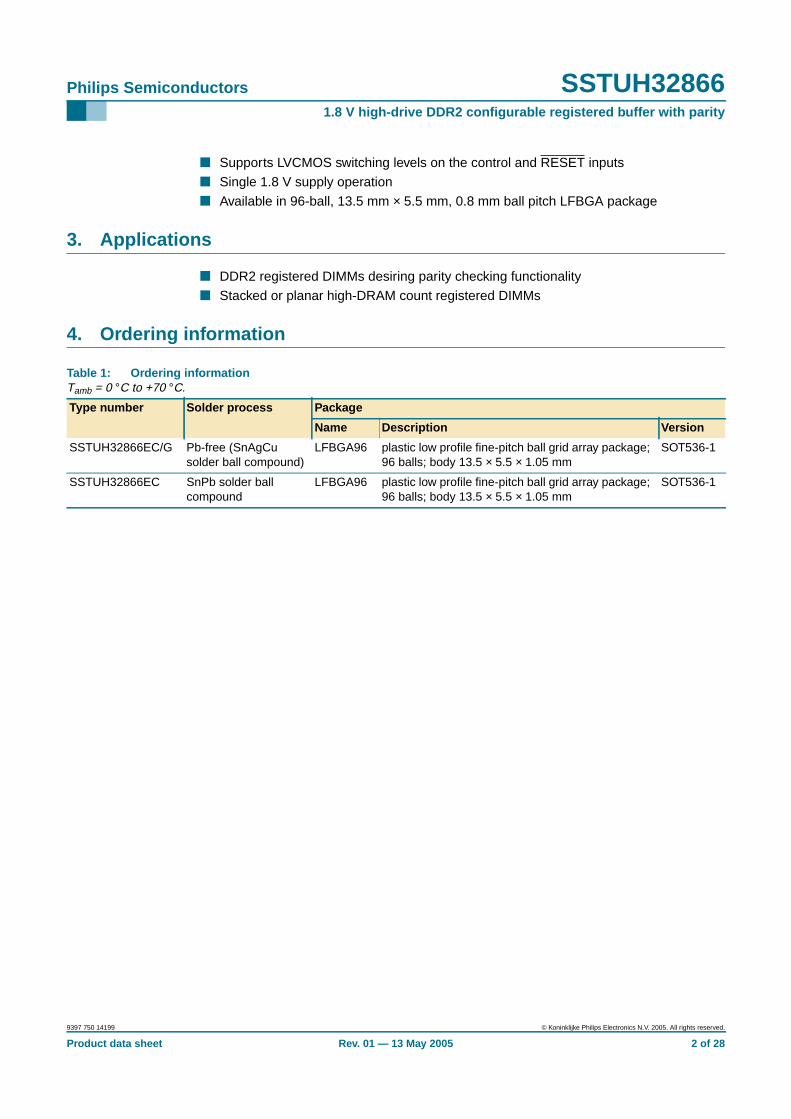
5. Functional diagram
(1) Disabled in 1 : 1 configuration.
Fig 1. Functional diagram of SSTUH32866; 1 : 2 Register A configuration with C0 = 0 andC1 = 1 (positive logic)
002aab328
1D
R
1D
R
1D
R
QCKEA
QCKEB(1)
QODTA
QODTB(1)
QCSA
QCSB(1)
C1
C1
C1
CSR
DCS
DODT
DCKE
D20
11D
R
Q2A
Q2B(1)C1
to 10 other channels(D3, D5, D6, D8 to D14)
CK
VREF
CK
RESET
SSTUH32866
9397 750 14199 © Koninklijke Philips Electronics N.V. 2005. All rights reserved.
Product data sheet Rev. 01 — 13 May 2005 3 of 28
Philips Semiconductors SSTUH328661.8 V high-drive DDR2 configurable registered buffer with parity
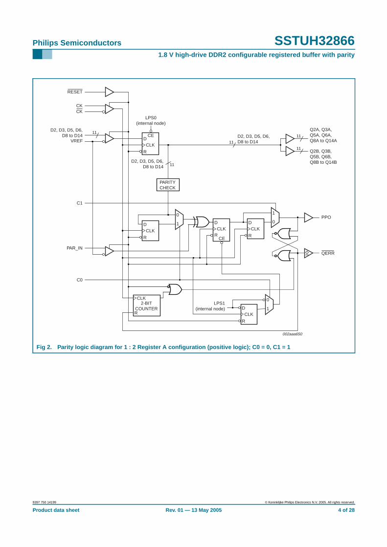
Fig 2. Parity logic diagram for 1 : 2 Register A configuration (positive logic); C0 = 0, C1 = 1
002aaa650
D
R
Q2A, Q3A,Q5A, Q6A,Q8A to Q14A
Q2B, Q3B,Q5B, Q6B,Q8B to Q14B
CLK
PAR_IN
D2, D3, D5, D6,D8 to D14
CKCK
RESET
LPS0(internal node)
CEVREF
PARITYCHECK
C1
0
1D
R
CLK
D
RCLK
CE
D
R
CLK
1
0
C0
R
CLK
D
R
CLK
LPS1(internal node)
0
12-BIT
COUNTER
QERR
PPO
D2, D3, D5, D6,D8 to D14
D2, D3, D5, D6,D8 to D14
11
11
11
11
11
9397 750 14199 © Koninklijke Philips Electronics N.V. 2005. All rights reserved.
Product data sheet Rev. 01 — 13 May 2005 4 of 28
Philips Semiconductors SSTUH328661.8 V high-drive DDR2 configurable registered buffer with parity
6. Pinning information
6.1 Pinning
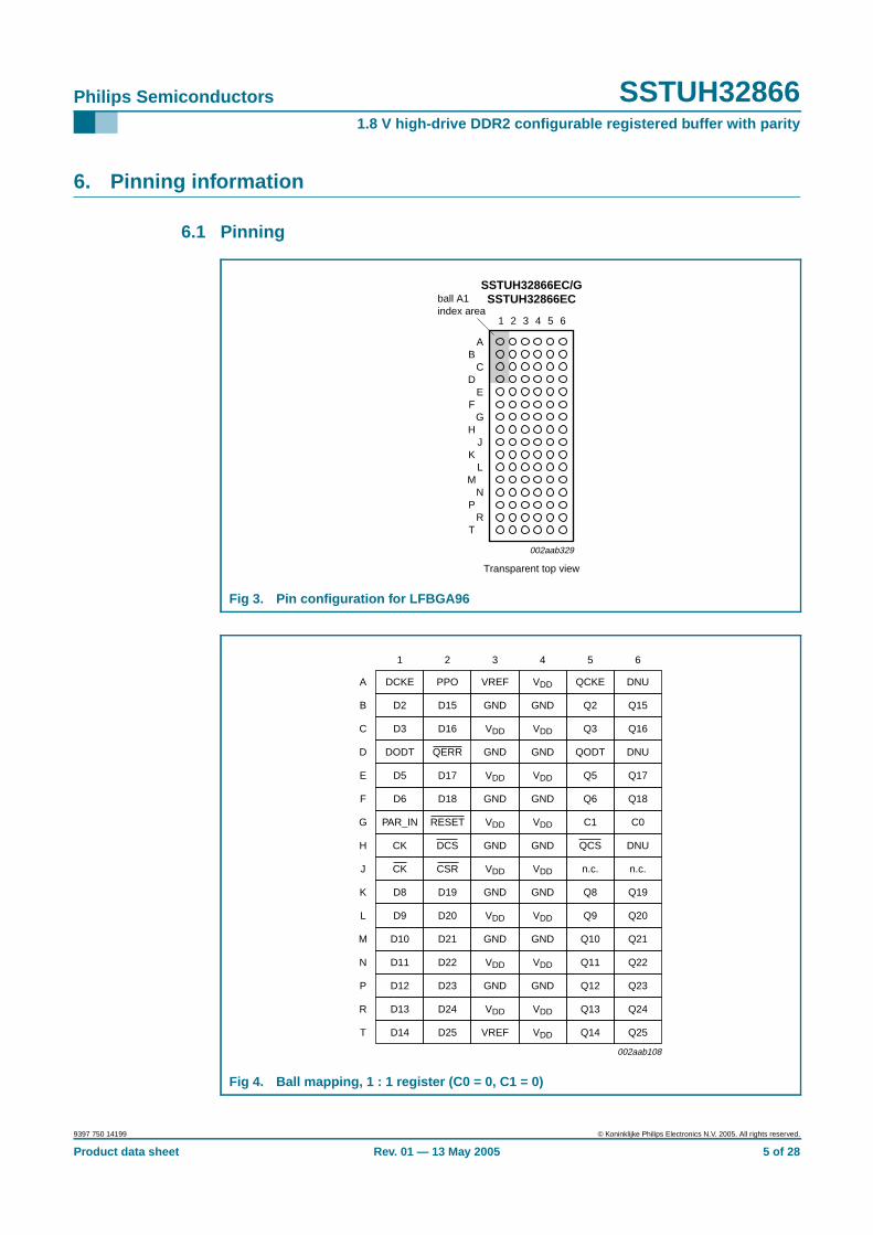
Fig 3. Pin configuration for LFBGA96
Fig 4. Ball mapping, 1 : 1 register (C0 = 0, C1 = 0)
002aab329
SSTUH32866EC/GSSTUH32866EC
Transparent top view
TR
PN
ML
J
G
K
H
FE
DC
BA
2 4 61 3 5
ball A1index area
DCKE PPO VREF VDD QCKE DNU
1 2 3 4 5 6
D2 D15 GND GND Q2 Q15
A
B
D3 D16 VDD VDD Q3 Q16C
DODT GND GND QODT DNUD
D5 D17 VDD VDD Q5 Q17E
D6 D18 GND GND Q6 Q18F
PAR_IN RESET VDD VDD C1 C0G
CK DCS GND GND QCS DNUH
CK CSR VDD VDD n.c. n.c.J
D8 D19 GND GND Q8 Q19K
D9 D20 VDD VDD Q9 Q20L
D10 D21 GND GND Q10 Q21M
D11 D22 VDD VDD Q11 Q22N
D12 D23 GND GND Q12 Q23P
D13 D24 VDD VDD Q13 Q24R
D14 D25 VREF VDD Q14 Q25T
002aab108
QERR
9397 750 14199 © Koninklijke Philips Electronics N.V. 2005. All rights reserved.
Product data sheet Rev. 01 — 13 May 2005 5 of 28
Philips Semiconductors SSTUH328661.8 V high-drive DDR2 configurable registered buffer with parity
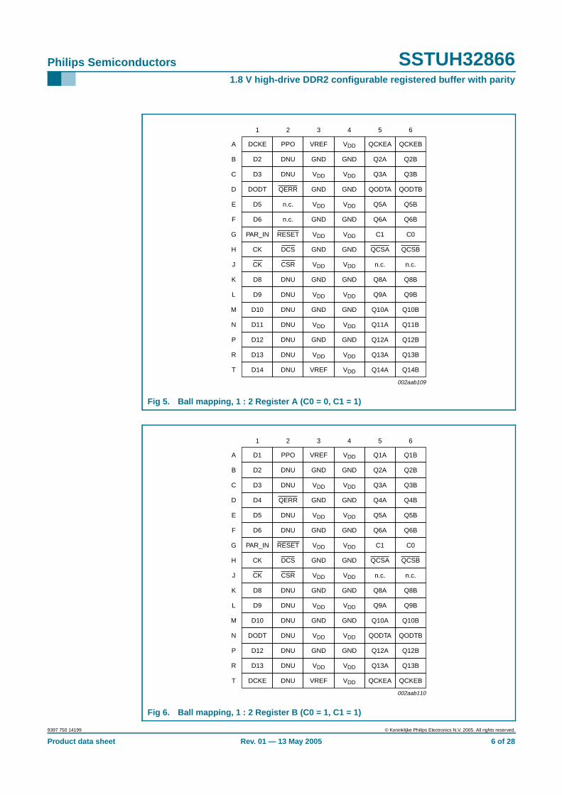
Fig 5. Ball mapping, 1 : 2 Register A (C0 = 0, C1 = 1)
Fig 6. Ball mapping, 1 : 2 Register B (C0 = 1, C1 = 1)
DCKE PPO VREF VDD QCKEA QCKEB
1 2 3 4 5 6
D2 DNU GND GND Q2A Q2B
A
B
D3 DNU VDD VDD Q3A Q3BC
DODT QERR GND GND QODTA QODTBD
D5 n.c. VDD VDD Q5A Q5BE
D6 n.c. GND GND Q6A Q6BF
PAR_IN RESET VDD VDD C1 C0G
CK DCS GND GND QCSAH
CK CSR VDD VDD n.c. n.c.J
D8 DNU GND GND Q8A Q8BK
D9 DNU VDD VDD Q9A Q9BL
D10 DNU GND GND Q10A Q10BM
D11 DNU VDD VDD Q11A Q11BN
D12 DNU GND GND Q12A Q12BP
D13 DNU VDD VDD Q13A Q13BR
D14 DNU VREF VDD Q14A Q14BT
002aab109
QCSB
D1 PPO VREF VDD Q1A Q1B
1 2 3 4 5 6
D2 DNU GND GND Q2A Q2B
A
B
D3 DNU VDD VDD Q3A Q3BC
D4 GND GND Q4A Q4BD
D5 DNU VDD VDD Q5A Q5BE
D6 DNU GND GND Q6A Q6BF
PAR_IN RESET VDD VDD C1 C0G
CK DCS GND GND QCSAH
CK CSR VDD VDD n.c. n.c.J
D8 DNU GND GND Q8A Q8BK
D9 DNU VDD VDD Q9A Q9BL
D10 DNU GND GND Q10A Q10BM
DODT DNU VDD VDD QODTA QODTBN
D12 DNU GND GND Q12A Q12BP
D13 DNU VDD VDD Q13A Q13BR
DCKE DNU VREF VDD QCKEA QCKEBT
002aab110
QCSB
QERR
9397 750 14199 © Koninklijke Philips Electronics N.V. 2005. All rights reserved.
Product data sheet Rev. 01 — 13 May 2005 6 of 28
Philips Semiconductors SSTUH328661.8 V high-drive DDR2 configurable registered buffer with parity
6.2 Pin description
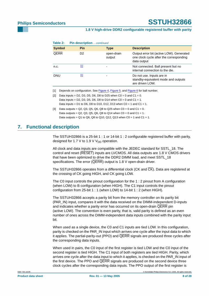
Table 2: Pin description
Symbol Pin Type Description
GND B3, B4, D3, D4,F3, F4, H3, H4,K3, K4, M3, M4,P3, P4
ground input ground
VDD A4, C3, C4, E3,E4, G3, G4, J3,J4, L3, L4, N3,N4, R3, R4, T4
1.8 V nominal power supply voltage
VREF A3, T3 0.9 V nominal input reference voltage
CK H1 Differential input positive master clock input
CK J1 Differential input negative master clock input
C0 G6 LVCMOS inputs Configuration control inputs; Register Aor Register B and 1 : 1 mode or 1 : 2mode select.
C1 G5
RESET G2 LVCMOS input Asynchronous reset input (active LOW).Resets registers and disables VREF dataand clock.
CSR J2 SSTL_18 input Chip select inputs (active LOW). DisablesD1 to D25 [2] outputs switching when bothinputs are HIGH.
DCS H2
D1 to D25 [1] SSTL_18 input Data input. Clocked in on the crossing ofthe rising edge of CK and the falling edgeof CK.
DODT [1] SSTL_18 input The outputs of this register bit will not besuspended by the DCS and CSR control.
DCKE [1] SSTL_18 input The outputs of this register bit will not besuspended by the DCS and CSR control.
PAR_IN G1 SSTL_18 input Parity input. Arrives one clock cycle afterthe corresponding data input.
Q1 to Q25,Q2A to Q14A,Q1B to Q14B
[1] 1.8 V CMOSoutputs
Data outputs that are suspended by theDCS and CSR control [3].
PPO A2 1.8 V CMOSoutput
Partial parity out. Indicates odd parity ofinputs D1 to D25 [2].
QCS, QCSA,QCSB
[1] 1.8 V CMOSoutput
Data output that will not be suspended bythe DCS and CSR control.
QODT, QODTA,QODTB
[1] 1.8 V CMOSoutput
Data output that will not be suspended bythe DCS and CSR control.
QCKE, QCKEA,QCKEB
[1] 1.8 V CMOSoutput
Data output that will not be suspended bythe DCS and CSR control.
9397 750 14199 © Koninklijke Philips Electronics N.V. 2005. All rights reserved.
Product data sheet Rev. 01 — 13 May 2005 7 of 28
Philips Semiconductors SSTUH328661.8 V high-drive DDR2 configurable registered buffer with parity
[1] Depends on configuration. See Figure 4, Figure 5, and Figure 6 for ball number.
[2] Data inputs = D2, D3, D5, D6, D8 to D25 when C0 = 0 and C1 = 0.
Data inputs = D2, D3, D5, D6, D8 to D14 when C0 = 0 and C1 = 1.
Data inputs = D1 to D6, D8 to D10, D12, D13 when C0 = 1 and C1 = 1.
[3] Data outputs = Q2, Q3, Q5, Q6, Q8 to Q25 when C0 = 0 and C1 = 0.
Data outputs = Q2, Q3, Q5, Q6, Q8 to Q14 when C0 = 0 and C1 = 1.
Data outputs = Q1 to Q6, Q8 to Q10, Q12, Q13 when C0 = 1 and C1 = 1.
7. Functional description
The SSTUH32866 is a 25-bit 1 : 1 or 14-bit 1 : 2 configurable registered buffer with parity,designed for 1.7 V to 1.9 V VDD operation.
All clock and data inputs are compatible with the JEDEC standard for SSTL_18. Thecontrol and reset (RESET) inputs are LVCMOS. All data outputs are 1.8 V CMOS driversthat have been optimized to drive the DDR2 DIMM load, and meet SSTL_18specifications. The error (QERR) output is 1.8 V open-drain driver.
The SSTUH32866 operates from a differential clock (CK and CK). Data are registered atthe crossing of CK going HIGH, and CK going LOW.
The C0 input controls the pinout configuration for the 1 : 2 pinout from A configuration(when LOW) to B configuration (when HIGH). The C1 input controls the pinoutconfiguration from 25-bit 1 : 1 (when LOW) to 14-bit 1 : 2 (when HIGH).
The SSTUH32866 accepts a parity bit from the memory controller on its parity bit(PAR_IN) input, compares it with the data received on the DIMM-independent D-inputsand indicates whether a parity error has occurred on its open-drain QERR pin(active LOW). The convention is even parity, that is, valid parity is defined as an evennumber of ones across the DIMM-independent data inputs combined with the parity inputbit.
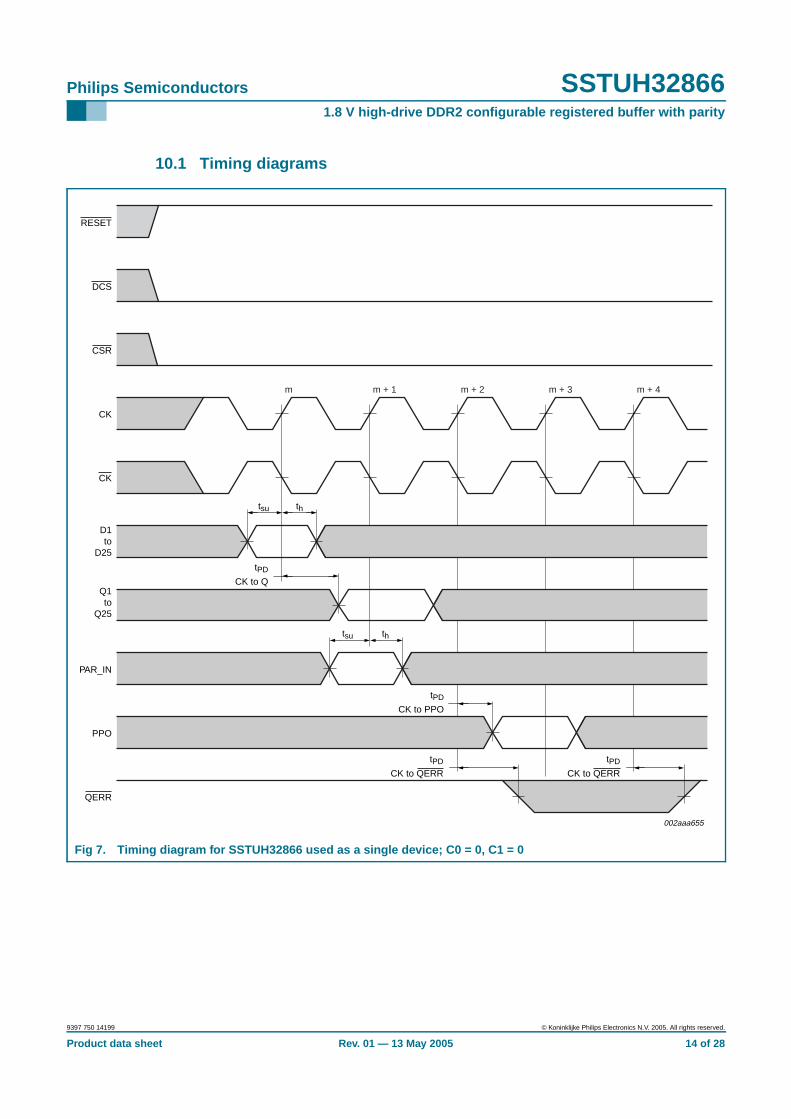
When used as a single device, the C0 and C1 inputs are tied LOW. In this configuration,parity is checked on the PAR_IN input which arrives one cycle after the input data to whichit applies. The partial-parity-out (PPO) and QERR signals are produced three cycles afterthe corresponding data inputs.
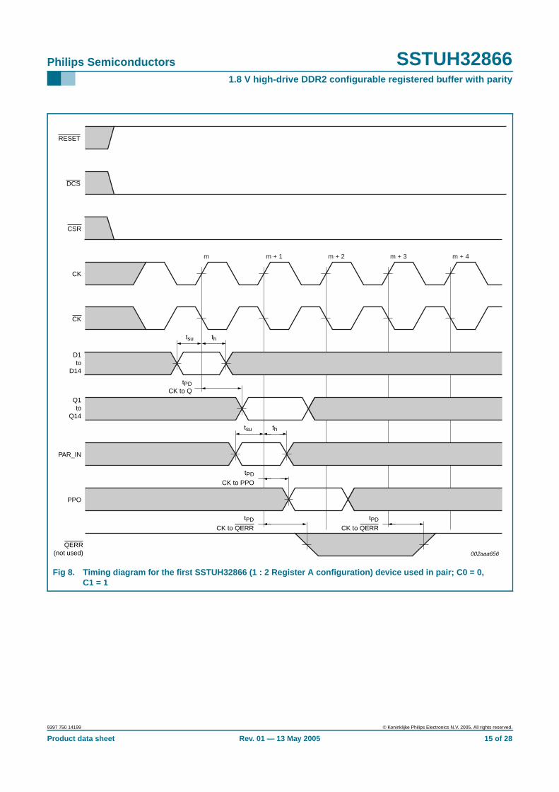
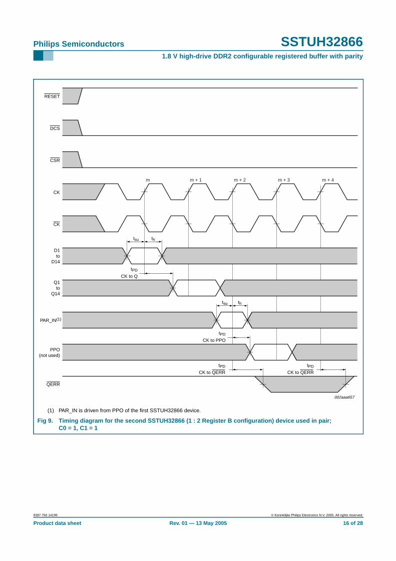
When used in pairs, the C0 input of the first register is tied LOW and the C0 input of thesecond register is tied HIGH. The C1 input of both registers are tied HIGH. Parity, whicharrives one cycle after the data input to which it applies, is checked on the PAR_IN input ofthe first device. The PPO and QERR signals are produced on the second device threeclock cycles after the corresponding data inputs. The PPO output of the first register is
QERR D2 open-drainoutput
Output error bit (active LOW). Generatedone clock cycle after the correspondingdata output
n.c. [1] - Not connected. Ball present but nointernal connection to the die.
DNU [1] - Do not use. Inputs are instandby-equivalent mode and outputsare driven LOW.
Table 2: Pin description …continued
Symbol Pin Type Description
9397 750 14199 © Koninklijke Philips Electronics N.V. 2005. All rights reserved.
Product data sheet Rev. 01 — 13 May 2005 8 of 28
Philips Semiconductors SSTUH328661.8 V high-drive DDR2 configurable registered buffer with parity
cascaded to the PAR_IN of the second register. The QERR output of the first register isleft floating and the valid error information is latched on the QERR output of the secondregister.
If an error occurs and the QERR output is driven LOW, it stays latched LOW for two clockcycles or until RESET is driven LOW. The DIMM-dependent signals (DCKE, DCS, DODT,and CSR) are not included in the parity check computation.
The device supports low-power standby operation. When RESET is LOW, the differentialinput receivers are disabled, and undriven (floating) data, clock and reference voltage(VREF) inputs are allowed. In addition, when RESET is LOW all registers are reset, andall outputs are forced LOW. The LVCMOS RESET input must always be held at a validlogic HIGH or LOW level.
The device also supports low-power active operation by monitoring both system chipselect (DCS and CSR) inputs and will gate the Qn and PPO outputs from changing stateswhen both DCS and CSR inputs are HIGH. If either DCS or CSR input is LOW, the Qnand PPO outputs will function normally. The RESET input has priority over the DCS andCSR control and when driven LOW will force the Qn and PPO outputs LOW, and theQERR output HIGH. If the DCS control functionality is not desired, then the CSR input canbe hard-wired to ground, in which case, the setup time requirement for DCS would be thesame as for the other Dn data inputs. To control the low-power mode with DCS only, thenthe CSR input should be pulled up to VDD through a pull-up resistor.
To ensure defined outputs from the register before a stable clock has been supplied,RESET must be held in the LOW state during power-up.
In the DDR2 RDIMM application, RESET is specified to be completely asynchronous withrespect to CK and CK. Therefore, no timing relationship can be guaranteed between thetwo. When entering reset, the register will be cleared and the Qn outputs will be drivenLOW quickly, relative to the time to disable the differential input receivers. However, whencoming out of reset, the register will become active quickly, relative to the time to enablethe differential input receivers. As long as the data inputs are LOW, and the clock is stableduring the time from the LOW-to-HIGH transition of RESET until the input receivers arefully enabled, the design of the SSTUH32866 must ensure that the outputs will remainLOW, thus ensuring no glitches on the output.
9397 750 14199 © Koninklijke Philips Electronics N.V. 2005. All rights reserved.
Product data sheet Rev. 01 — 13 May 2005 9 of 28
Philips Semiconductors SSTUH328661.8 V high-drive DDR2 configurable registered buffer with parity
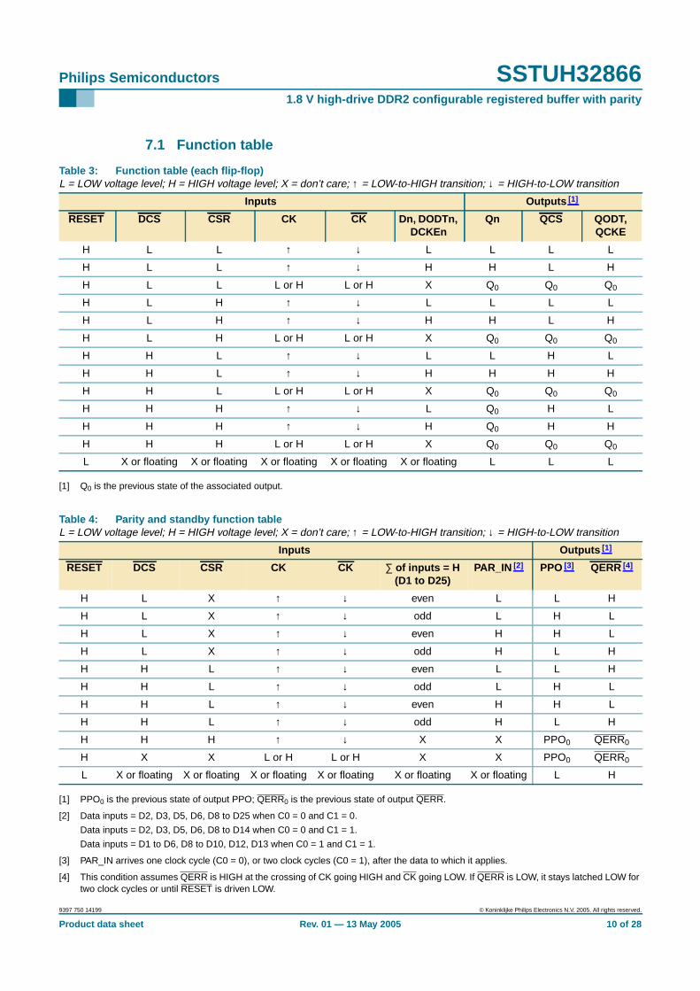
7.1 Function table
[1] Q0 is the previous state of the associated output.
[1] PPO0 is the previous state of output PPO; QERR0 is the previous state of output QERR.
[2] Data inputs = D2, D3, D5, D6, D8 to D25 when C0 = 0 and C1 = 0.
Data inputs = D2, D3, D5, D6, D8 to D14 when C0 = 0 and C1 = 1.
Data inputs = D1 to D6, D8 to D10, D12, D13 when C0 = 1 and C1 = 1.
[3] PAR_IN arrives one clock cycle (C0 = 0), or two clock cycles (C0 = 1), after the data to which it applies.
[4] This condition assumes QERR is HIGH at the crossing of CK going HIGH and CK going LOW. If QERR is LOW, it stays latched LOW fortwo clock cycles or until RESET is driven LOW.
Table 3: Function table (each flip-flop)L = LOW voltage level; H = HIGH voltage level; X = don’t care; ↑ = LOW-to-HIGH transition; ↓ = HIGH-to-LOW transition
Inputs Outputs [1]
RESET DCS CSR CK CK Dn, DODTn,DCKEn
Qn QCS QODT,QCKE
H L L ↑ ↓ L L L L
H L L ↑ ↓ H H L H
H L L L or H L or H X Q0 Q0 Q0
H L H ↑ ↓ L L L L
H L H ↑ ↓ H H L H
H L H L or H L or H X Q0 Q0 Q0
H H L ↑ ↓ L L H L
H H L ↑ ↓ H H H H
H H L L or H L or H X Q0 Q0 Q0
H H H ↑ ↓ L Q0 H L
H H H ↑ ↓ H Q0 H H
H H H L or H L or H X Q0 Q0 Q0
L X or floating X or floating X or floating X or floating X or floating L L L
Table 4: Parity and standby function tableL = LOW voltage level; H = HIGH voltage level; X = don’t care; ↑ = LOW-to-HIGH transition; ↓ = HIGH-to-LOW transition
Inputs Outputs [1]
RESET DCS CSR CK CK ∑ of inputs = H(D1 to D25)
PAR_IN [2] PPO [3] QERR [4]
H L X ↑ ↓ even L L H
H L X ↑ ↓ odd L H L
H L X ↑ ↓ even H H L
H L X ↑ ↓ odd H L H
H H L ↑ ↓ even L L H
H H L ↑ ↓ odd L H L
H H L ↑ ↓ even H H L
H H L ↑ ↓ odd H L H
H H H ↑ ↓ X X PPO0 QERR0
H X X L or H L or H X X PPO0 QERR0
L X or floating X or floating X or floating X or floating X or floating X or floating L H
9397 750 14199 © Koninklijke Philips Electronics N.V. 2005. All rights reserved.
Product data sheet Rev. 01 — 13 May 2005 10 of 28
Philips Semiconductors SSTUH328661.8 V high-drive DDR2 configurable registered buffer with parity
8. Limiting values
[1] The input and output negative-voltage ratings may be exceeded if the input and output clamp-current ratings are observed.
[2] This value is limited to 2.5 V maximum.
9. Recommended operating conditions
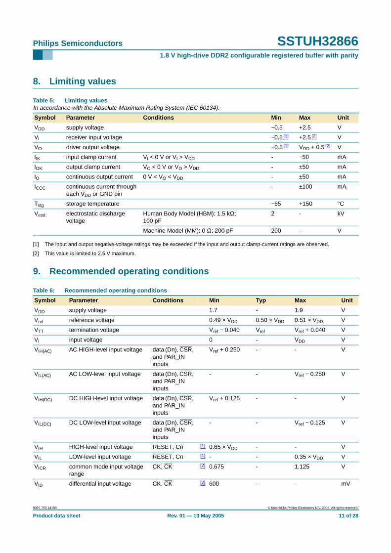
Table 5: Limiting valuesIn accordance with the Absolute Maximum Rating System (IEC 60134).
Symbol Parameter Conditions Min Max Unit
VDD supply voltage −0.5 +2.5 V
VI receiver input voltage −0.5 [1] +2.5 [2] V
VO driver output voltage −0.5 [1] VDD + 0.5 [2] V
IIK input clamp current VI < 0 V or VI > VDD - −50 mA
IOK output clamp current VO < 0 V or VO > VDD - ±50 mA
IO continuous output current 0 V < VO < VDD - ±50 mA
ICCC continuous current througheach VDD or GND pin
- ±100 mA
Tstg storage temperature −65 +150 °C
Vesd electrostatic dischargevoltage
Human Body Model (HBM); 1.5 kΩ;100 pF
2 - kV
Machine Model (MM); 0 Ω; 200 pF 200 - V
Table 6: Recommended operating conditions
Symbol Parameter Conditions Min Typ Max Unit
VDD supply voltage 1.7 - 1.9 V
Vref reference voltage 0.49 × VDD 0.50 × VDD 0.51 × VDD V
VTT termination voltage Vref − 0.040 Vref Vref + 0.040 V
VI input voltage 0 - VDD V
VIH(AC) AC HIGH-level input voltage data (Dn), CSR,and PAR_INinputs
Vref + 0.250 - - V
VIL(AC) AC LOW-level input voltage data (Dn), CSR,and PAR_INinputs
- - Vref − 0.250 V
VIH(DC) DC HIGH-level input voltage data (Dn), CSR,and PAR_INinputs
Vref + 0.125 - - V
VIL(DC) DC LOW-level input voltage data (Dn), CSR,and PAR_INinputs
- - Vref − 0.125 V
VIH HIGH-level input voltage RESET, Cn [1] 0.65 × VDD - - V
VIL LOW-level input voltage RESET, Cn [1] - - 0.35 × VDD V
VICR common mode input voltagerange
CK, CK [2] 0.675 - 1.125 V
VID differential input voltage CK, CK [2] 600 - - mV
9397 750 14199 © Koninklijke Philips Electronics N.V. 2005. All rights reserved.
Product data sheet Rev. 01 — 13 May 2005 11 of 28

Philips Semiconductors SSTUH328661.8 V high-drive DDR2 configurable registered buffer with parity
[1] The RESET and Cn inputs of the device must be held at valid levels (not floating) to ensure proper device operation.
[2] The differential inputs must not be floating, unless RESET is LOW.
10. Characteristics
IOH HIGH-level output current - - −12 mA
IOL LOW-level output current - - 12 mA
Tamb ambient temperature operating infree air
0 - +70 °C
Table 6: Recommended operating conditions …continued
Symbol Parameter Conditions Min Typ Max Unit
Table 7: CharacteristicsAt recommended operating conditions (see Table 6), unless otherwise specified.
Symbol Parameter Conditions Min Typ Max Unit
VOH HIGH-level output voltage IOH = −12 mA; VDD = 1.7 V 1.2 - - V
VOL LOW-level output voltage IOL = 12 mA; VDD = 1.7 V - - 0.5 V
II input current all inputs; VI = VDD or GND;VDD = 1.9 V
- - ±5 µA
IDD static standby current RESET = GND; IO = 0 mA;VDD = 1.9 V
- - 100 µA
static operating current RESET = VDD; IO = 0 mA;VDD = 1.9 V; VI = VIH(AC) or VIL(AC)
- - 40 mA
IDDD dynamic operating current per MHz,clock only
RESET = VDD;VI = VIH(AC) or VIL(AC); CK and CKswitching at 50 % duty cycle.IO = 0 mA; VDD = 1.8 V
- 16 - µA
dynamic operating current per MHz,per each data input, 1 : 1 mode
RESET = VDD;VI = VIH(AC) or VIL(AC); CK and CKswitching at 50 % duty cycle. Onedata input switching at half clockfrequency, 50 % duty cycle.IO = 0 mA; VDD = 1.8 V
- 11 - µA
dynamic operating current per MHz,per each data input, 1 : 2 mode
RESET = VDD;VI = VIH(AC) or VIL(AC); CK and CKswitching at 50 % duty cycle. Onedata input switching at half clockfrequency, 50 % duty cycle.IO = 0 mA; VDD = 1.8 V
- 19 - µA
Ci input capacitance, data and CSRinputs
VI = Vref ± 250 mV; VDD = 1.8 V 2.5 - 3.5 pF
input capacitance,CK and CK inputs
VICR = 0.9 V; Vi(p-p) = 600 mV;VDD = 1.8 V
2 - 3 pF
input capacitance, RESET input VI = VDD or GND; VDD = 1.8 V 3 - 4 pF
9397 750 14199 © Koninklijke Philips Electronics N.V. 2005. All rights reserved.
Product data sheet Rev. 01 — 13 May 2005 12 of 28
Philips Semiconductors SSTUH328661.8 V high-drive DDR2 configurable registered buffer with parity
[1] This parameter is not necessarily production tested.
[2] VREF must be held at a valid input voltage level and data inputs must be held LOW for a minimum time of tACT(max) after RESET is takenHIGH.
[3] VREF, data and clock inputs must be held at valid levels (not floating) a minimum time of tINACT(max) after RESET is taken LOW.
[1] Includes 350 ps of test-load transmission line delay.
[2] This parameter is not necessarily production tested.
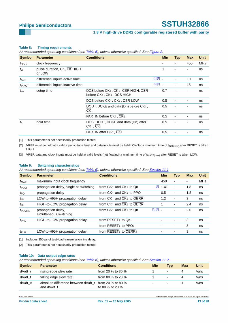
Table 8: Timing requirementsAt recommended operating conditions (see Table 6), unless otherwise specified. See Figure 2.
Symbol Parameter Conditions Min Typ Max Unit
fclock clock frequency - - 450 MHz
tW pulse duration, CK, CK HIGHor LOW
1 - - ns
tACT differential inputs active time [1] [2] - - 10 ns
tINACT differential inputs inactive time [1] [3] - - 15 ns
tsu setup time DCS before CK↑, CK↓, CSR HIGH; CSRbefore CK↑, CK↓, DCS HIGH
0.7 - - ns
DCS before CK↑, CK↓, CSR LOW 0.5 - - ns
DODT, DCKE and data (Dn) before CK↑,CK↓
0.5 - - ns
PAR_IN before CK↑, CK↓ 0.5 - - ns
th hold time DCS, DODT, DCKE and data (Dn) afterCK↑, CK↓
0.5 - - ns
PAR_IN after CK↑, CK↓ 0.5 - - ns
Table 9: Switching characteristicsAt recommended operating conditions (see Table 6), unless otherwise specified. See Section 11.1.
Symbol Parameter Conditions Min Typ Max Unit
fMAX maximum input clock frequency 450 - - MHz
tPDM propagation delay, single bit switching from CK↑ and CK↓ to Qn [1] 1.41 - 1.8 ns
tPD propagation delay from CK↑ and CK↓ to PPO 0.5 - 1.8 ns
tLH LOW-to-HIGH propagation delay from CK↑ and CK↓ to QERR 1.2 - 3 ns
tHL HIGH-to-LOW propagation delay from CK↑ and CK↓ to QERR 1 - 2.4 ns
tPDMSS propagation delay,simultaneous switching
from CK↑ and CK↓ to Qn [1] [2] - - 2.0 ns
tPHL HIGH-to-LOW propagation delay from RESET↓ to Qn↓ - - 3 ns
from RESET↓ to PPO↓ - - 3 ns
tPLH LOW-to-HIGH propagation delay from RESET↓ to QERR↑ - - 3 ns
Table 10: Data output edge ratesAt recommended operating conditions (see Table 6), unless otherwise specified. See Section 11.2.
Symbol Parameter Conditions Min Typ Max Unit
dV/dt_r rising edge slew rate from 20 % to 80 % 1 - 4 V/ns
dV/dt_f falling edge slew rate from 80 % to 20 % 1 - 4 V/ns
dV/dt_∆ absolute difference between dV/dt_rand dV/dt_f
from 20 % or 80 %to 80 % or 20 %
- - 1 V/ns
9397 750 14199 © Koninklijke Philips Electronics N.V. 2005. All rights reserved.
Product data sheet Rev. 01 — 13 May 2005 13 of 28
Philips Semiconductors SSTUH328661.8 V high-drive DDR2 configurable registered buffer with parity
10.1 Timing diagrams
Fig 7. Timing diagram for SSTUH32866 used as a single device; C0 = 0, C1 = 0
RESET
DCS
CSR
CK
CK
D1to
D25
Q1to
Q25
PAR_IN
PPO
QERR
tsu th
m m + 1 m + 2 m + 3 m + 4
tPD
CK to Q
tsu th
tPD
CK to PPO
tPD
CK to QERR
002aaa655
tPD
CK to QERR
9397 750 14199 © Koninklijke Philips Electronics N.V. 2005. All rights reserved.
Product data sheet Rev. 01 — 13 May 2005 14 of 28
Philips Semiconductors SSTUH328661.8 V high-drive DDR2 configurable registered buffer with parity
Fig 8. Timing diagram for the first SSTUH32866 (1 : 2 Register A configuration) device used in pair; C0 = 0,C1 = 1
RESET
DCS
CSR
CK
CK
D1to
D14
Q1to
Q14
PAR_IN
PPO
QERR(not used)
tsu th
m m + 1 m + 2 m + 3 m + 4
tPDCK to Q
tsu th
tPD
CK to PPO
tPD
CK to QERR
002aaa656
tPD
CK to QERR
9397 750 14199 © Koninklijke Philips Electronics N.V. 2005. All rights reserved.
Product data sheet Rev. 01 — 13 May 2005 15 of 28
Philips Semiconductors SSTUH328661.8 V high-drive DDR2 configurable registered buffer with parity
(1) PAR_IN is driven from PPO of the first SSTUH32866 device.
Fig 9. Timing diagram for the second SSTUH32866 (1 : 2 Register B configuration) device used in pair;C0 = 1, C1 = 1
RESET
DCS
CSR
CK
CK
D1to
D14
Q1to
Q14
PAR_IN(1)
PPO(not used)
QERR
tsu th
m m + 1 m + 2 m + 3 m + 4
tPD
CK to Q
tsu th
tPD
CK to PPO
tPD
CK to QERR
002aaa657
tPD
CK to QERR
9397 750 14199 © Koninklijke Philips Electronics N.V. 2005. All rights reserved.
Product data sheet Rev. 01 — 13 May 2005 16 of 28
Philips Semiconductors SSTUH328661.8 V high-drive DDR2 configurable registered buffer with parity
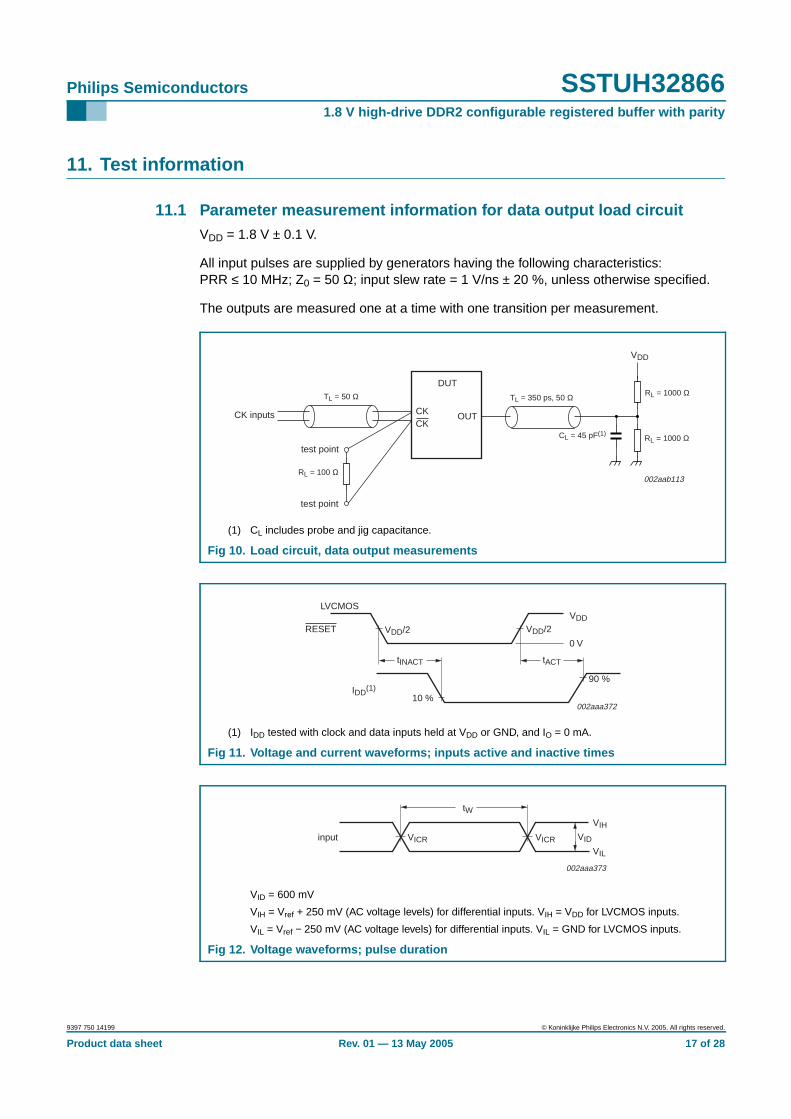
11. Test information
11.1 Parameter measurement information for data output load circuitVDD = 1.8 V ± 0.1 V.
All input pulses are supplied by generators having the following characteristics:PRR ≤ 10 MHz; Z0 = 50 Ω; input slew rate = 1 V/ns ± 20 %, unless otherwise specified.
The outputs are measured one at a time with one transition per measurement.
(1) CL includes probe and jig capacitance.
Fig 10. Load circuit, data output measurements
(1) IDD tested with clock and data inputs held at VDD or GND, and IO = 0 mA.
Fig 11. Voltage and current waveforms; inputs active and inactive times
VID = 600 mV
VIH = Vref + 250 mV (AC voltage levels) for differential inputs. VIH = VDD for LVCMOS inputs.
VIL = Vref − 250 mV (AC voltage levels) for differential inputs. VIL = GND for LVCMOS inputs.
Fig 12. Voltage waveforms; pulse duration
RL = 100 Ω
RL = 1000 Ω
VDD
TL = 50 Ω
CK inputsCKCK OUT
DUT
test point
002aab113
test point
TL = 350 ps, 50 Ω
RL = 1000 ΩCL = 45 pF(1)
LVCMOS
RESET
10 %IDD
(1)
tINACT
VDDVDD/2
tACT
90 %
0 V
002aaa372
VDD/2
VICR VICR
VIH
VIL
input
tW
VID
002aaa373
9397 750 14199 © Koninklijke Philips Electronics N.V. 2005. All rights reserved.
Product data sheet Rev. 01 — 13 May 2005 17 of 28
Philips Semiconductors SSTUH328661.8 V high-drive DDR2 configurable registered buffer with parity
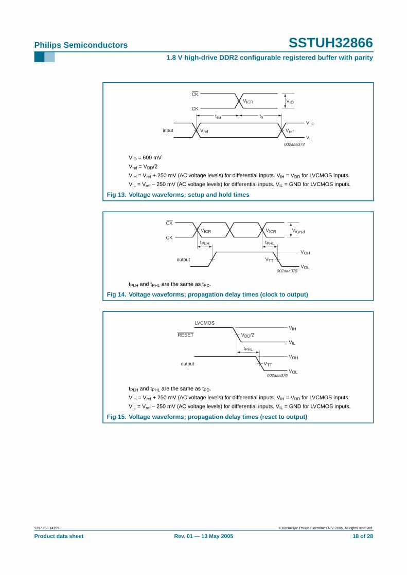
VID = 600 mV
Vref = VDD/2
VIH = Vref + 250 mV (AC voltage levels) for differential inputs. VIH = VDD for LVCMOS inputs.
VIL = Vref − 250 mV (AC voltage levels) for differential inputs. VIL = GND for LVCMOS inputs.
Fig 13. Voltage waveforms; setup and hold times
tPLH and tPHL are the same as tPD.
Fig 14. Voltage waveforms; propagation delay times (clock to output)
tPLH and tPHL are the same as tPD.
VIH = Vref + 250 mV (AC voltage levels) for differential inputs. VIH = VDD for LVCMOS inputs.
VIL = Vref − 250 mV (AC voltage levels) for differential inputs. VIL = GND for LVCMOS inputs.
Fig 15. Voltage waveforms; propagation delay times (reset to output)
tsu
VIH
VIL
VID
th
CK
CK
input Vref Vref
VICR
002aaa374
VOH
VOL
output
tPLH
002aaa375
VTT
VICR VICR
tPHL
CK
CK
Vi(p-p)
tPHL
002aaa376
LVCMOS
RESET
output VTT
VDD/2
VIH
VIL
VOH
VOL
9397 750 14199 © Koninklijke Philips Electronics N.V. 2005. All rights reserved.
Product data sheet Rev. 01 — 13 May 2005 18 of 28
Philips Semiconductors SSTUH328661.8 V high-drive DDR2 configurable registered buffer with parity
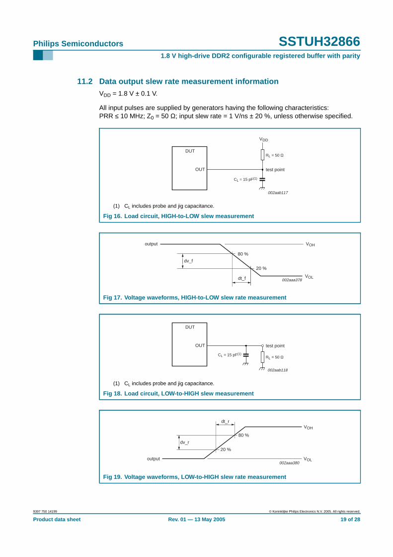
11.2 Data output slew rate measurement informationVDD = 1.8 V ± 0.1 V.
All input pulses are supplied by generators having the following characteristics:PRR ≤ 10 MHz; Z0 = 50 Ω; input slew rate = 1 V/ns ± 20 %, unless otherwise specified.
(1) CL includes probe and jig capacitance.
Fig 16. Load circuit, HIGH-to-LOW slew measurement
Fig 17. Voltage waveforms, HIGH-to-LOW slew rate measurement
(1) CL includes probe and jig capacitance.
Fig 18. Load circuit, LOW-to-HIGH slew measurement
Fig 19. Voltage waveforms, LOW-to-HIGH slew rate measurement
CL = 15 pF(1)
VDD
OUT
DUT
test point
RL = 50 Ω
002aab117
VOH
VOL
output
80 %
20 %
dv_f
dt_f 002aaa378
CL = 15 pF(1)
OUT
DUT
test point
RL = 50 Ω
002aab118
VOH
VOL
80 %
20 %
dv_r
dt_r
output002aaa380
9397 750 14199 © Koninklijke Philips Electronics N.V. 2005. All rights reserved.
Product data sheet Rev. 01 — 13 May 2005 19 of 28
Philips Semiconductors SSTUH328661.8 V high-drive DDR2 configurable registered buffer with parity
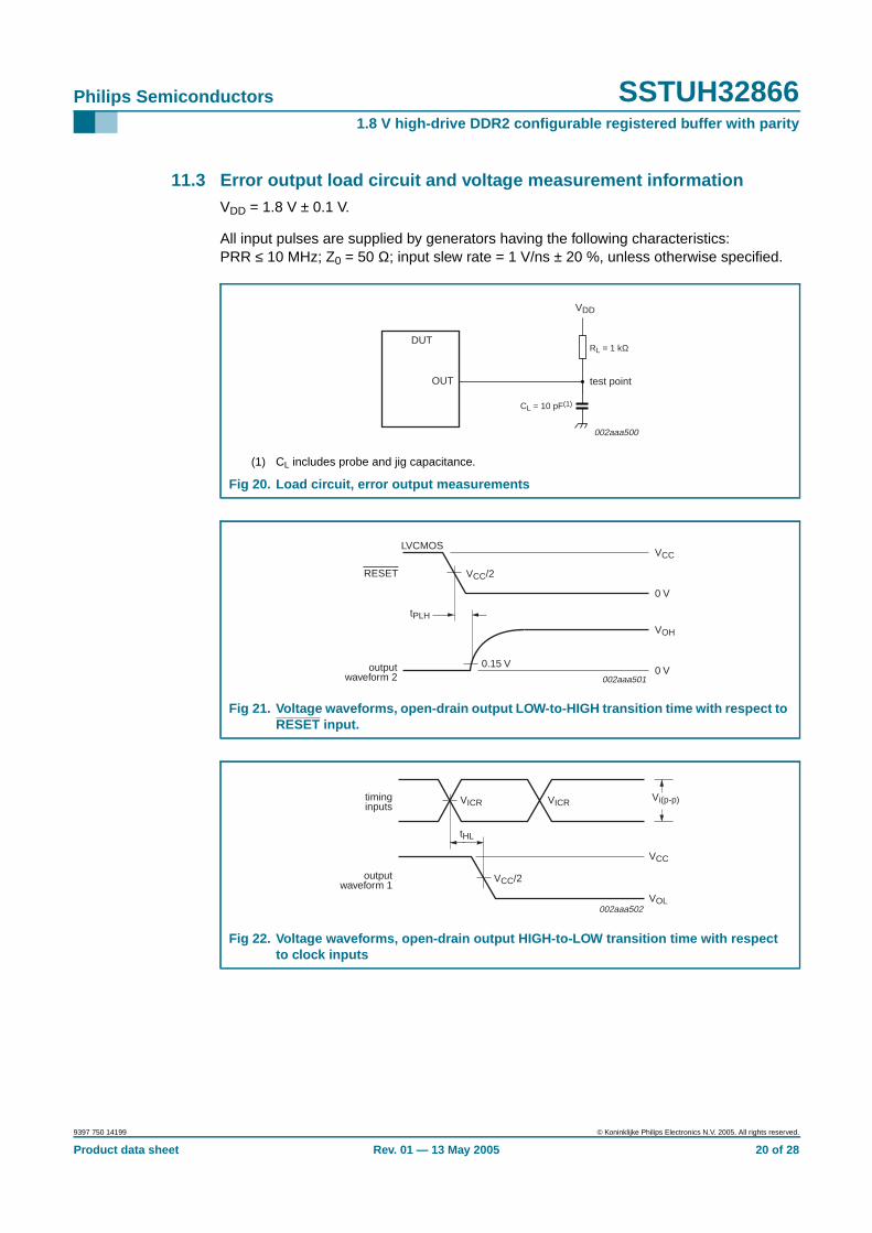
11.3 Error output load circuit and voltage measurement informationVDD = 1.8 V ± 0.1 V.
All input pulses are supplied by generators having the following characteristics:PRR ≤ 10 MHz; Z0 = 50 Ω; input slew rate = 1 V/ns ± 20 %, unless otherwise specified.
(1) CL includes probe and jig capacitance.
Fig 20. Load circuit, error output measurements
Fig 21. Voltage waveforms, open-drain output LOW-to-HIGH transition time with respect toRESET input.
Fig 22. Voltage waveforms, open-drain output HIGH-to-LOW transition time with respectto clock inputs
CL = 10 pF(1)
VDD
OUT
DUT
test point
RL = 1 kΩ
002aaa500
VCC/2
tPLH
VCC
0 V
0.15 V
VOH
0 Voutputwaveform 2
RESET
002aaa501
LVCMOS
VICR
tHL
VCC/2
VCC
VOL
timinginputs
outputwaveform 1
Vi(p-p)VICR
002aaa502
9397 750 14199 © Koninklijke Philips Electronics N.V. 2005. All rights reserved.
Product data sheet Rev. 01 — 13 May 2005 20 of 28
Philips Semiconductors SSTUH328661.8 V high-drive DDR2 configurable registered buffer with parity
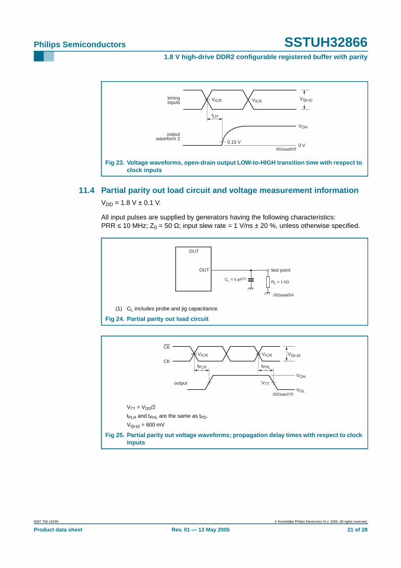
11.4 Partial parity out load circuit and voltage measurement informationVDD = 1.8 V ± 0.1 V.
All input pulses are supplied by generators having the following characteristics:PRR ≤ 10 MHz; Z0 = 50 Ω; input slew rate = 1 V/ns ± 20 %, unless otherwise specified.
Fig 23. Voltage waveforms, open-drain output LOW-to-HIGH transition time with respect toclock inputs
VICR
tLH
VOH
0 V
timinginputs
outputwaveform 2
Vi(p-p)VICR
0.15 V
002aaa503
(1) CL includes probe and jig capacitance.
Fig 24. Partial parity out load circuit
VTT = VDD/2
tPLH and tPHL are the same as tPD.
Vi(p-p) = 600 mV
Fig 25. Partial parity out voltage waveforms; propagation delay times with respect to clockinputs
CL = 5 pF(1)
OUT
DUT
test point
RL = 1 kΩ
002aaa654
VOH
VOL
output
tPLH
002aaa375
VTT
VICR VICR
tPHL
CK
CK
Vi(p-p)
9397 750 14199 © Koninklijke Philips Electronics N.V. 2005. All rights reserved.
Product data sheet Rev. 01 — 13 May 2005 21 of 28

Philips Semiconductors SSTUH328661.8 V high-drive DDR2 configurable registered buffer with parity
VTT = VDD/2
tPLH and tPHL are the same as tPD.
VIH = Vref + 250 mV (AC voltage levels) for differential inputs. VIH = VDD for LVCMOS inputs.
VIL = Vref − 250 mV (AC voltage levels) for differential inputs. VIL = VDD for LVCMOS inputs.
Fig 26. Partial parity out voltage waveforms; propagation delay times with respect toRESET input
tPHL
002aaa376
LVCMOS
RESET
output VTT
VDD/2
VIH
VIL
VOH
VOL
9397 750 14199 © Koninklijke Philips Electronics N.V. 2005. All rights reserved.
Product data sheet Rev. 01 — 13 May 2005 22 of 28
Philips Semiconductors SSTUH328661.8 V high-drive DDR2 configurable registered buffer with parity
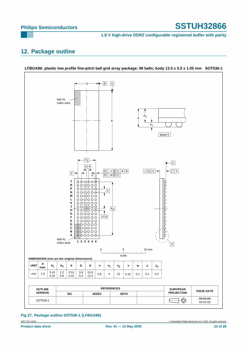
12. Package outline
Fig 27. Package outline SOT536-1 (LFBGA96)
0.8
A1 bA2UNIT D ye
REFERENCESOUTLINEVERSION
EUROPEANPROJECTION ISSUE DATE
00-03-0403-02-05
IEC JEDEC JEITA
mm 1.5 0.410.31
1.20.9
5.65.4
y1
13.613.4
0.510.41
0.1 0.2
e1
4
e2
12
DIMENSIONS (mm are the original dimensions)
SOT536-1
E
0.15
v
0.1
w
0 5 10 mm
scale
SOT536-1LFBGA96: plastic low profile fine-pitch ball grid array package; 96 balls; body 13.5 x 5.5 x 1.05 mm
Amax.
AA2
A1
detail X
e
e
X
D
E
ABCDEF
HG
JKLM
PN
RT
2 4 61 3 5
B A
e2
e1
ball A1index area
ball A1index area
yy1 C
b
C
ACC
B∅ v M
∅ w M
1/2 e
1/2 e
9397 750 14199 © Koninklijke Philips Electronics N.V. 2005. All rights reserved.
Product data sheet Rev. 01 — 13 May 2005 23 of 28
Philips Semiconductors SSTUH328661.8 V high-drive DDR2 configurable registered buffer with parity
13. Soldering
13.1 Introduction to soldering surface mount packagesThis text gives a very brief insight to a complex technology. A more in-depth account ofsoldering ICs can be found in our Data Handbook IC26; Integrated Circuit Packages(document order number 9398 652 90011).
There is no soldering method that is ideal for all surface mount IC packages. Wavesoldering can still be used for certain surface mount ICs, but it is not suitable for fine pitchSMDs. In these situations reflow soldering is recommended.
13.2 Reflow solderingReflow soldering requires solder paste (a suspension of fine solder particles, flux andbinding agent) to be applied to the printed-circuit board by screen printing, stencilling orpressure-syringe dispensing before package placement. Driven by legislation andenvironmental forces the worldwide use of lead-free solder pastes is increasing.
Several methods exist for reflowing; for example, convection or convection/infraredheating in a conveyor type oven. Throughput times (preheating, soldering and cooling)vary between 100 seconds and 200 seconds depending on heating method.
Typical reflow peak temperatures range from 215 °C to 270 °C depending on solder pastematerial. The top-surface temperature of the packages should preferably be kept:
• below 225 °C (SnPb process) or below 245 °C (Pb-free process)
– for all BGA, HTSSON..T and SSOP..T packages
– for packages with a thickness ≥ 2.5 mm
– for packages with a thickness < 2.5 mm and a volume ≥ 350 mm3 so calledthick/large packages.
• below 240 °C (SnPb process) or below 260 °C (Pb-free process) for packages with athickness < 2.5 mm and a volume < 350 mm3 so called small/thin packages.
Moisture sensitivity precautions, as indicated on packing, must be respected at all times.
13.3 Wave solderingConventional single wave soldering is not recommended for surface mount devices(SMDs) or printed-circuit boards with a high component density, as solder bridging andnon-wetting can present major problems.
To overcome these problems the double-wave soldering method was specificallydeveloped.
If wave soldering is used the following conditions must be observed for optimal results:
• Use a double-wave soldering method comprising a turbulent wave with high upwardpressure followed by a smooth laminar wave.
• For packages with leads on two sides and a pitch (e):
– larger than or equal to 1.27 mm, the footprint longitudinal axis is preferred to beparallel to the transport direction of the printed-circuit board;
9397 750 14199 © Koninklijke Philips Electronics N.V. 2005. All rights reserved.
Product data sheet Rev. 01 — 13 May 2005 24 of 28
Philips Semiconductors SSTUH328661.8 V high-drive DDR2 configurable registered buffer with parity
– smaller than 1.27 mm, the footprint longitudinal axis must be parallel to thetransport direction of the printed-circuit board.
The footprint must incorporate solder thieves at the downstream end.
• For packages with leads on four sides, the footprint must be placed at a 45° angle tothe transport direction of the printed-circuit board. The footprint must incorporatesolder thieves downstream and at the side corners.
During placement and before soldering, the package must be fixed with a droplet ofadhesive. The adhesive can be applied by screen printing, pin transfer or syringedispensing. The package can be soldered after the adhesive is cured.
Typical dwell time of the leads in the wave ranges from 3 seconds to 4 seconds at 250 °Cor 265 °C, depending on solder material applied, SnPb or Pb-free respectively.
A mildly-activated flux will eliminate the need for removal of corrosive residues in mostapplications.
13.4 Manual solderingFix the component by first soldering two diagonally-opposite end leads. Use a low voltage(24 V or less) soldering iron applied to the flat part of the lead. Contact time must belimited to 10 seconds at up to 300 °C.
When using a dedicated tool, all other leads can be soldered in one operation within2 seconds to 5 seconds between 270 °C and 320 °C.
13.5 Package related soldering information
[1] For more detailed information on the BGA packages refer to the (LF)BGA Application Note (AN01026);order a copy from your Philips Semiconductors sales office.
[2] All surface mount (SMD) packages are moisture sensitive. Depending upon the moisture content, themaximum temperature (with respect to time) and body size of the package, there is a risk that internal orexternal package cracks may occur due to vaporization of the moisture in them (the so called popcorneffect). For details, refer to the Drypack information in the Data Handbook IC26; Integrated CircuitPackages; Section: Packing Methods.
[3] These transparent plastic packages are extremely sensitive to reflow soldering conditions and must on noaccount be processed through more than one soldering cycle or subjected to infrared reflow soldering withpeak temperature exceeding 217 °C ± 10 °C measured in the atmosphere of the reflow oven. The packagebody peak temperature must be kept as low as possible.
Table 11: Suitability of surface mount IC packages for wave and reflow soldering methods
Package [1] Soldering method
Wave Reflow [2]
BGA, HTSSON..T [3], LBGA, LFBGA, SQFP,SSOP..T [3], TFBGA, VFBGA, XSON
not suitable suitable
DHVQFN, HBCC, HBGA, HLQFP, HSO, HSOP,HSQFP, HSSON, HTQFP, HTSSOP, HVQFN,HVSON, SMS
not suitable [4] suitable
PLCC [5], SO, SOJ suitable suitable
LQFP, QFP, TQFP not recommended [5] [6] suitable
SSOP, TSSOP, VSO, VSSOP not recommended [7] suitable
CWQCCN..L [8], PMFP [9], WQCCN..L [8] not suitable not suitable
9397 750 14199 © Koninklijke Philips Electronics N.V. 2005. All rights reserved.
Product data sheet Rev. 01 — 13 May 2005 25 of 28
Philips Semiconductors SSTUH328661.8 V high-drive DDR2 configurable registered buffer with parity
[4] These packages are not suitable for wave soldering. On versions with the heatsink on the bottom side, thesolder cannot penetrate between the printed-circuit board and the heatsink. On versions with the heatsinkon the top side, the solder might be deposited on the heatsink surface.
[5] If wave soldering is considered, then the package must be placed at a 45° angle to the solder wavedirection. The package footprint must incorporate solder thieves downstream and at the side corners.
[6] Wave soldering is suitable for LQFP, QFP and TQFP packages with a pitch (e) larger than 0.8 mm; it isdefinitely not suitable for packages with a pitch (e) equal to or smaller than 0.65 mm.
[7] Wave soldering is suitable for SSOP, TSSOP, VSO and VSSOP packages with a pitch (e) equal to or largerthan 0.65 mm; it is definitely not suitable for packages with a pitch (e) equal to or smaller than 0.5 mm.
[8] Image sensor packages in principle should not be soldered. They are mounted in sockets or deliveredpre-mounted on flex foil. However, the image sensor package can be mounted by the client on a flex foil byusing a hot bar soldering process. The appropriate soldering profile can be provided on request.
[9] Hot bar soldering or manual soldering is suitable for PMFP packages.
14. Abbreviations
15. Revision history
Table 12: Abbreviations
Acronym Description
CMOS Complementary Metal Oxide Silicon
DDR Double Data Rate
DIMM Dual In-line Memory Module
DRAM Dynamic Random Access Memory
JEDEC Joint Electron Device Engineering Council
LFBGA Low profile Fine-pitch Ball Grid Array
LVCMOS Low Voltage Complementary Metal Oxide Silicon
PPO Partial Parity Out
PRR Pulse Repetition Rate
RDIMM Registered Dual In-line Memory Module
SSTL Stub Series Terminated Logic
Table 13: Revision history
Document ID Release date Data sheet status Change notice Doc. number Supersedes
SSTUH32866_1 20050513 Product data sheet - 9397 750 14199 -
9397 750 14199 © Koninklijke Philips Electronics N.V. 2005. All rights reserved.
Product data sheet Rev. 01 — 13 May 2005 26 of 28
Philips Semiconductors SSTUH328661.8 V high-drive DDR2 configurable registered buffer with parity
16. Data sheet status
[1] Please consult the most recently issued data sheet before initiating or completing a design.
[2] The product status of the device(s) described in this data sheet may have changed since this data sheet was published. The latest information is available on the Internet atURL http://www.semiconductors.philips.com.
[3] For data sheets describing multiple type numbers, the highest-level product status determines the data sheet status.
17. Definitions
Short-form specification — The data in a short-form specification isextracted from a full data sheet with the same type number and title. Fordetailed information see the relevant data sheet or data handbook.
Limiting values definition — Limiting values given are in accordance withthe Absolute Maximum Rating System (IEC 60134). Stress above one ormore of the limiting values may cause permanent damage to the device.These are stress ratings only and operation of the device at these or at anyother conditions above those given in the Characteristics sections of thespecification is not implied. Exposure to limiting values for extended periodsmay affect device reliability.
Application information — Applications that are described herein for anyof these products are for illustrative purposes only. Philips Semiconductorsmake no representation or warranty that such applications will be suitable forthe specified use without further testing or modification.
18. Disclaimers
Life support — These products are not designed for use in life supportappliances, devices, or systems where malfunction of these products canreasonably be expected to result in personal injury. Philips Semiconductors
customers using or selling these products for use in such applications do soat their own risk and agree to fully indemnify Philips Semiconductors for anydamages resulting from such application.
Right to make changes — Philips Semiconductors reserves the right tomake changes in the products - including circuits, standard cells, and/orsoftware - described or contained herein in order to improve design and/orperformance. When the product is in full production (status ‘Production’),relevant changes will be communicated via a Customer Product/ProcessChange Notification (CPCN). Philips Semiconductors assumes noresponsibility or liability for the use of any of these products, conveys nolicense or title under any patent, copyright, or mask work right to theseproducts, and makes no representations or warranties that these products arefree from patent, copyright, or mask work right infringement, unless otherwisespecified.
19. Trademarks
Notice — All referenced brands, product names, service names andtrademarks are the property of their respective owners.
20. Contact information
For additional information, please visit: http://www.semiconductors.philips.com
For sales office addresses, send an email to: [email protected]
Level Data sheet status [1] Product status [2] [3] Definition
I Objective data Development This data sheet contains data from the objective specification for product development. PhilipsSemiconductors reserves the right to change the specification in any manner without notice.
II Preliminary data Qualification This data sheet contains data from the preliminary specification. Supplementary data will be publishedat a later date. Philips Semiconductors reserves the right to change the specification without notice, inorder to improve the design and supply the best possible product.
III Product data Production This data sheet contains data from the product specification. Philips Semiconductors reserves theright to make changes at any time in order to improve the design, manufacturing and supply. Relevantchanges will be communicated via a Customer Product/Process Change Notification (CPCN).
9397 750 14199 © Koninklijke Philips Electronics N.V. 2005. All rights reserved.
Product data sheet Rev. 01 — 13 May 2005 27 of 28
Philips Semiconductors SSTUH328661.8 V high-drive DDR2 configurable registered buffer with parity
21. Contents
1 General description . . . . . . . . . . . . . . . . . . . . . . 12 Features . . . . . . . . . . . . . . . . . . . . . . . . . . . . . . . 13 Applications . . . . . . . . . . . . . . . . . . . . . . . . . . . . 24 Ordering information . . . . . . . . . . . . . . . . . . . . . 25 Functional diagram . . . . . . . . . . . . . . . . . . . . . . 36 Pinning information . . . . . . . . . . . . . . . . . . . . . . 56.1 Pinning . . . . . . . . . . . . . . . . . . . . . . . . . . . . . . . 56.2 Pin description . . . . . . . . . . . . . . . . . . . . . . . . . 77 Functional description . . . . . . . . . . . . . . . . . . . 87.1 Function table . . . . . . . . . . . . . . . . . . . . . . . . . 108 Limiting values. . . . . . . . . . . . . . . . . . . . . . . . . 119 Recommended operating conditions. . . . . . . 1110 Characteristics . . . . . . . . . . . . . . . . . . . . . . . . . 1210.1 Timing diagrams . . . . . . . . . . . . . . . . . . . . . . . 1411 Test information . . . . . . . . . . . . . . . . . . . . . . . . 1711.1 Parameter measurement information for data
output load circuit . . . . . . . . . . . . . . . . . . . . . . 1711.2 Data output slew rate measurement
information . . . . . . . . . . . . . . . . . . . . . . . . . . . 1911.3 Error output load circuit and voltage
measurement information . . . . . . . . . . . . . . . . 2011.4 Partial parity out load circuit and voltage
measurement information . . . . . . . . . . . . . . . . 2112 Package outline . . . . . . . . . . . . . . . . . . . . . . . . 2313 Soldering . . . . . . . . . . . . . . . . . . . . . . . . . . . . . 2413.1 Introduction to soldering surface mount
packages . . . . . . . . . . . . . . . . . . . . . . . . . . . . 2413.2 Reflow soldering . . . . . . . . . . . . . . . . . . . . . . . 2413.3 Wave soldering . . . . . . . . . . . . . . . . . . . . . . . . 2413.4 Manual soldering . . . . . . . . . . . . . . . . . . . . . . 2513.5 Package related soldering information . . . . . . 2514 Abbreviations . . . . . . . . . . . . . . . . . . . . . . . . . . 2615 Revision history . . . . . . . . . . . . . . . . . . . . . . . . 2616 Data sheet status . . . . . . . . . . . . . . . . . . . . . . . 2717 Definitions . . . . . . . . . . . . . . . . . . . . . . . . . . . . 2718 Disclaimers. . . . . . . . . . . . . . . . . . . . . . . . . . . . 2719 Trademarks. . . . . . . . . . . . . . . . . . . . . . . . . . . . 2720 Contact information . . . . . . . . . . . . . . . . . . . . 27
© Koninklijke Philips Electronics N.V. 2005All rights are reserved. Reproduction in whole or in part is prohibited without the priorwritten consent of the copyright owner. The information presented in this document doesnot form part of any quotation or contract, is believed to be accurate and reliable and maybe changed without notice. No liability will be accepted by the publisher for anyconsequence of its use. Publication thereof does not convey nor imply any license underpatent- or other industrial or intellectual property rights.
Date of release: 13 May 2005Document number: 9397 750 14199
Published in The Netherlands