Embed Size (px)
Citation preview

Advancing Communication Technology:
Spread Spectrum CDMA
SystemVue 2011
Agilent EEsof EDA
© Agilent Technologies, Inc., 2012

Spread Spectrum CDMA © Agilent Technologies, Inc., 2012
Anticipate__Accelerate__Achieve 1
Spread Spectrum CDMA
Table of Contents
1. Lab 1: Bit Generation Pattern ............................................................................................................... 3
2. Lab 2: Mapping.................................................................................................................................... 10
3. Lab 3: Walsh Code ............................................................................................................................... 13
4. Lab 4: Filter Design .............................................................................................................................. 16
5. Lab 5: Modulation ............................................................................................................................... 20
6. Lab 6: RF Link....................................................................................................................................... 22
7. Lab 7: Step7 Demodulation ................................................................................................................. 27
8. Lab8: Completed System .................................................................................................................... 33
9. Conclusion ........................................................................................................................................... 39
10. Appendix 1 ...................................................................................................................................... 40

Spread Spectrum CDMA © Agilent Technologies, Inc., 2012
Anticipate__Accelerate__Achieve 2
CDMA Systems allow users to simultaneously transmit data over the same frequency band. In this transmission technique, the frequency spectrum of a data signal is spread using a special coding scheme (where each user is assigned a code). This tutorial builds and examines the design process of a simple spread spectrum system (CDMA) and exposes all necessary tools to simulate, display and analyse critical aspects of the system using SystemVue.
CDMA is a form of a Direct Sequence Spread Spectrum (where the transmitted data is coded at a very high frequency) communication. In spread spectrum, to send data, the signal bandwidth is much larger than necessary to support multi-user access. In addition the large bandwidth ensures interference of other users does not occur. Multi user access is achieved using a code that is pseudo-random. A pseudo-random code is generated using a special coding generator to separate different users. The code appears random but is in fact known allowing the receiver to reconstruct the code. In this tutorial the pseudo-random code is generated using a Walsh code generator from an orthogonal set of codes.
During signal transmission, the data signal is modulated with the pseudo code and the resultant signal modulates a carrier. The carrier is then amplified and broadcasted.
At the receiving end, the carrier is received and amplified. The signal information from the coded signal is then recovered by correlating the received code with a generated code (the same Walsh code at the transmission) at the receiver. Thus the receiver can reconstruct the code, extracting the transmitted data.
This tutorial is comprised of 8 step by step lab sessions leading to a final completed digital modulation system. Using BER to assess the performance of our CDMA Spread Spectrum System, we can observe our bit stream over our designed communication channel.

Spread Spectrum CDMA © Agilent Technologies, Inc., 2012
Anticipate__Accelerate__Achieve 3
1. Lab 1: Bit Generation Pattern In this lab we will create a very simple bit generation pattern and analyse its output in the form of an eye diagram.
1. Start SystemVue 2011.10 by double clicking on the desktop icon. 2. After loading, the “welcome” page featuring intuitive tutorial videos will appear-for now let’s
skip this, click close 3. The next window allows you to open existing workspaces or templates. For this session, click
“cancel” to create a blank workspace.
This will bring the schematic window where your design work will take place. Top of the screen presents the toolbar; on the left hand side you will see a directory structure which is your “workspace tree”. The workspace tree allows you to organise designs, displays, equations, etc. by employment of a hierarchy folder structure. Below the workspace tree, is the “tune window” which is one of the most powerful features of SystemVue allowing you to use tuned variables (real-time tuning of values in variables) anywhere in your design. The right hand side displays a library of parts (called Part Selector). At the bottom of the screen, information of errors is displayed-also notice the tabs placed below the error screen showing other log info).
Let us begin....
Workspace tree Part Selector
Tune Window
Error/info window

Spread Spectrum CDMA © Agilent Technologies, Inc., 2012
Anticipate__Accelerate__Achieve 4
File>Save As> My_CDMA_Sys, this will save the entire work session by name “My_CDMA_Sys”. It is a good idea to save the workspace after each lab by performing File>Save.
By default SystemVue would have created a folder and populated it with a design and an analysis. Rename the folder “Designs” by placing mouse cursor over “Designs” folder, Right Click> Rename... Give it the name “Step1_Bits”. Rename the schematic Design1 as “Bits” and Design Analysis as “DF_Bits” (this is the design flow analysis that gathers information about the set of values set and runs a design program-similar to a compiler).
Double Click on “DF_Bits” and enter the following values:
The key parameter is System Sample Rate. The other essential parameter is the Number Samples which determines the length of simulation. Start and Stop times are automatically set. The frequency resolution is calculated from Stop Time.
1. Press “Ok” to dismiss the window 2. Maximise the design workspace to full screen 3. From “Part Selector A”, type “Bits” into the “filter by” field and press “enter”. You will be shown
all the parts related to the word “Bits”. Single Click on “Bits” and move your cursor across to the blank schematic. Click again to release the part
4. Double Click on the “Bits” Part. One of the nice and perceptive features of SystemVue is that most parts are polymorphic models
Setting these two fields will automatically set the rest
Ensure that these fields match the dataset name given
Spread Spectrum CDMA © Agilent Technologies, Inc., 2012
Anticipate__Accelerate__Achieve 5
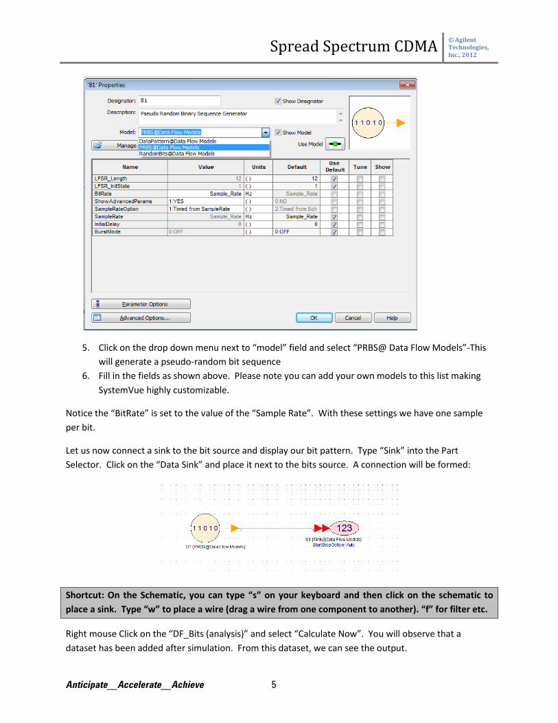
5. Click on the drop down menu next to “model” field and select “PRBS@ Data Flow Models”-This will generate a pseudo-random bit sequence
6. Fill in the fields as shown above. Please note you can add your own models to this list making SystemVue highly customizable.
Notice the “BitRate” is set to the value of the “Sample Rate”. With these settings we have one sample per bit.
Let us now connect a sink to the bit source and display our bit pattern. Type “Sink” into the Part Selector. Click on the “Data Sink” and place it next to the bits source. A connection will be formed:
Shortcut: On the Schematic, you can type “s” on your keyboard and then click on the schematic to place a sink. Type “w” to place a wire (drag a wire from one component to another). “f” for filter etc.
Right mouse Click on the “DF_Bits (analysis)” and select “Calculate Now”. You will observe that a dataset has been added after simulation. From this dataset, we can see the output.

Spread Spectrum CDMA © Agilent Technologies, Inc., 2012
Anticipate__Accelerate__Achieve 6
To keep organised Right Click on the dataset> Rename... Call it “DF1_Bits”
Since the dataset name has now been changed, we must ensure that the data analysis simulates the correct dataset.
7. Double Click on the analysis “DF_Bits”> next to field Dataset>Type “DF1_Bits”>Click Ok
Notice that Data Flow and Dataset are now coloured in red. This means that the simulation is not up to date as we have made a change to our design.
8. Right Click on “DF_Bits”>Run(Calculate Now)
Upon errorless simulation, let’s graph the bits:
9. Double Click on the dataset “DF1_Bits” to open it and you will see variables corresponding to the sink
10. Right mouse Click on S1>Add to Graph>New Graph Series Wizard
11. Under “select type of series” choose “Time”. Ensure that in the field box “Data Selected”, “S1” is checked boxed as this is the output we wish to graph

Spread Spectrum CDMA © Agilent Technologies, Inc., 2012
Anticipate__Accelerate__Achieve 7
12. Press Ok, this will bring up a graph properties dialog with S1 as the only variable to be plotted (Called MyVar)
13. Press Ok. This will lead you to plot our design “Bits” in time domain

Spread Spectrum CDMA © Agilent Technologies, Inc., 2012
Anticipate__Accelerate__Achieve 8
14. You can use your mouse wheel to zoom in on the x-axis of the graph. As you scroll forward, you should gradually see the random 1s and 0s more clearly (as shown above)
Eye diagrams are often used in communication to give designers an insight about signal characteristics.
1. Modify the schematic to match below by copying the “Bits” schematic created previously (check that the same parts used have the same variables as before):
2. The BitFormat can be found in part selector by typing “NRZ” into the search field. Similarly for IID Uniform Noise Source, type “Noise” and the Adder can be withdrawn from the parts library by searching for “Add”. NRZ part will transform the digital bits to a voltage of our choice; we have added some noise to make the eye diagram more interesting and realistic.
3. Double Click on the noise source and set the LoLevel voltage to -0.4V and the HiLevel voltage to 0.4V. This can be achieved by clicking on the fields and entering the values.
4. Simulate the design (Right click on “DF_Bits”>Run) 5. Double Click on the dataset and right mouse click on S2>Add to Graph>New Graph Series
Wizard>Eye>Custom Equations. Modify equations to: SymbolRate = 1e6; % in Hz NumCycles = 3; % Number of cycles to plot before wrapping StartUpDelay = 2; % Number of start up samples that will be
removed
6. Click Ok three times to dismiss the windows. You should now see an eye diagram:

Spread Spectrum CDMA © Agilent Technologies, Inc., 2012
Anticipate__Accelerate__Achieve 9
You can modify the graph by double clicking on it; this will bring up the graph properties dialog. Notice that variable “y” has been named with context “<post proceed>”. This means that you can post proceed your time domain data to generate the eye diagram. Pressing “edit” within the dialog window will take you back to the graph wizard where you can modify equations to alter your graph.
Lab1 is now complete
Save your workspace!

Spread Spectrum CDMA © Agilent Technologies, Inc., 2012
Anticipate__Accelerate__Achieve 10
2. Lab 2: Mapping In this lab we will map the bit data onto one of the popular digital modulation format. We will view the plot on a constellation diagram.
Create a new folder called “Step2_Mapping”:
1. Right Click on path “My_CDMA_Sys”(this is placed at the top of the workspace tree)>Add>Add Folder>Give it the name “Step2_Mapping”
2. Right Click on the folder “Step2_Mapping”>Add>Designs>Add Schematic> Name the design “Mapping”
3. Add a dataset, Right Click on the folder “Step2_Mapping”>Add>Add Data>Name it “DF1_Mapping”
4. Right Click on the folder “Step2_Mapping”>Add>Analysis>Add DataFlow Analysis>Call it “DF_Mapping”. Within the DataFlow Analysis pop window, ensure that the design and dataset fields correspond to this simulation:
In schematic view, let’s map the bits using QPSK modulation as shown below. For the Bits part, be sure to set the parameters as you did in Lab 1, #4, page 4.

Spread Spectrum CDMA © Agilent Technologies, Inc., 2012
Anticipate__Accelerate__Achieve 11
Run the Simulation:
5. Right Click on “DF_Mapping”>Run(Calculate Now) 6. Double Click on the dataset and right mouse click on the sink (S1)>Add to Graph>New Graph
Series Wizard>Constellation>Ok>Ok again
You should see a perfect constellation diagram:
We can add some noise to the system and see what happens to the constellation diagram.
7. Modify your design:
Type “map” into part selector

Spread Spectrum CDMA © Agilent Technologies, Inc., 2012
Anticipate__Accelerate__Achieve 12
N.B It can be good practice to name wires for neatness (we will later explore another benefit), for this right click on the wire>Net> Edit Net name (here I have chosen the name Ref)
8. Now run the simulation (Right Click “DF_Mapping”>Run) 9. Navigate back to the previous graph made and you will see the noise added to the constellation:
End of Lab 2

Spread Spectrum CDMA © Agilent Technologies, Inc., 2012
Anticipate__Accelerate__Achieve 13
3. Lab 3: Walsh Code In this lab we will generate a Walsh code for our data signal
1. Right Click “My_CDMA_Sys”>Add>Add folder. Name it “Step3_WalshCode” 2. Right Click on folder “Step3_WalshCode”>Add>Designs>Add Schematic. Name the schematic
“WalshCode” 3. Right Click on folder “Step3_WalshCode”>Add>Analysis>Data Flow Analysis. Call it
“DF_WalshCode”. 4. Right Click on folder “Step3_WalshCode”>Add>Add Data. Title it “DF1_WalshCode” 5. Double Click on the Data Flow Analysis and alter parameters so that the ‘design’ and ‘dataset’
are coherent i.e. The design field reads “WalshCode” and the dataset field reads “DF1_WalshCode”. All other parameters should match the analysis previously set.
Copy the schematic from “Step2_Mapping” and modify the design as shown below:
After the data is plotted for mapping, the symbol rate is reduced by a factor of 4 (due to dual polarization and QPSK). An up sampler increases the sample rate back a certain factor. In this case we up sample by a factor of 8 so the symbol rate is 4 MHz giving us sufficient bandwidth to transmit on for the carrier and over the communication channel.
6. Double Click on the Up Sample part>Set the factor of the value to 8. Set the mode to be “HoldSample” (the input sample is repeated by a factor of 8 at the output).
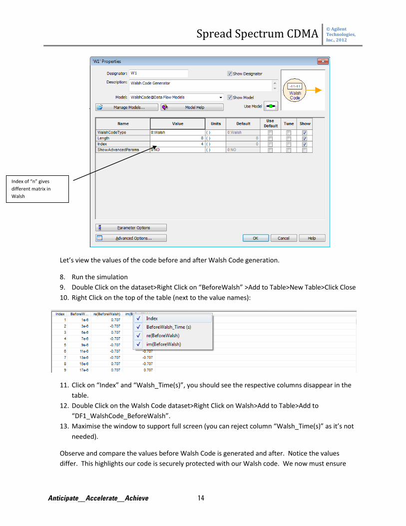
7. Double Click on WalshCode Generator part. Set the following values:
Name the sink “BeforeWalsh”>enter “BeforeWalsh in “designator” field
Call this “Walsh”
Spread Spectrum CDMA © Agilent Technologies, Inc., 2012
Anticipate__Accelerate__Achieve 14
Let’s view the values of the code before and after Walsh Code generation.
8. Run the simulation 9. Double Click on the dataset>Right Click on “BeforeWalsh” >Add to Table>New Table>Click Close 10. Right Click on the top of the table (next to the value names):
11. Click on “Index” and “Walsh_Time(s)”, you should see the respective columns disappear in the table.
12. Double Click on the Walsh Code dataset>Right Click on Walsh>Add to Table>Add to “DF1_WalshCode_BeforeWalsh”.
13. Maximise the window to support full screen (you can reject column “Walsh_Time(s)” as it’s not needed).
Observe and compare the values before Walsh Code is generated and after. Notice the values differ. This highlights our code is securely protected with our Walsh code. We now must ensure
Index of “n” gives different matrix in Walsh

Spread Spectrum CDMA © Agilent Technologies, Inc., 2012
Anticipate__Accelerate__Achieve 15
that the same Walsh code is applied at the receiving end to decode our data and retrieve the original code of information. During the final lab we will use some examples and look at what happens to individual bits as they are correlated with Walsh coding.
Additional Exercise:
Change the index of the Walsh Code Generator via properties. Create the table of values again of before WalshCode generation and after-notice the difference in values
Lab 3 is finished

Spread Spectrum CDMA © Agilent Technologies, Inc., 2012
Anticipate__Accelerate__Achieve 16
4. Lab 4: Filter Design In this lab we will create a folder which will conserve the modulated bandwidth.
1. Create a folder and call it “Step5_Filter” 2. Add a schematic design called “Filter” 3. Add a data flow analysis and call it “DF_Filter”. Set Number of Samples to 4096 (see page 4). 4. Add a dataset and name it “DF1_Filter”
Copy the schematic created in Step3 and paste it into the new black schematic created. Modify the design as shown below:
5. Double click on the filter part. This should bring up the design properties. Select Filter Designer button. Change the properties to match the below. Close the property page once you have completed the changes.
Type “filter” into part selector
Sink renamed Filter
Sink renamed Walsh

Spread Spectrum CDMA © Agilent Technologies, Inc., 2012
Anticipate__Accelerate__Achieve 17
Run the analysis>Double click on the filter dataset (DF1_Filter)>Right Click on Walsh>Add to Graph>New Graph Wizard>Spectrum>Press Ok three times:

Spread Spectrum CDMA © Agilent Technologies, Inc., 2012
Anticipate__Accelerate__Achieve 18
Now plot a spectra graph for “Filter”. Double click on the filter dataset (DF1_Filter)>Right Click on Filter>Add to Graph>New Graph Wizard>Spectrum>Press Ok three times:
Spread Spectrum CDMA © Agilent Technologies, Inc., 2012
Anticipate__Accelerate__Achieve 19
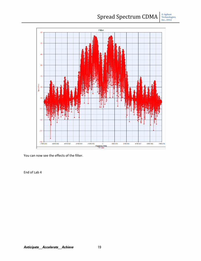
You can now see the effects of the filter.
End of Lab 4

Spread Spectrum CDMA © Agilent Technologies, Inc., 2012
Anticipate__Accelerate__Achieve 20
5. Lab 5: Modulation 6. Create a new folder called “Step5_Modulation”; add a new schematic called “Modulation”.
With it add a data flow analysis (“DF_Modulation”) and a dataset (“DF1_Modulation”). Set Number of Samples to 4096 of data flow analysis (see page 4).
1. Copy the schematic created in Step 4 and paste it in the new blank schematic 2. Delete the “output” sink 3. In part selector search for component “cxt” and select the part “Cxt To Rect” (this will separate
the real and imaginary parts of the signal) 4. Place it adjacent to the output of the filter 5. Add a modulator (type “modulator” in the part selector library) 6. Place it at the output of the complex to real and imaginary convertor. 7. Place a noise density part (type “noise density” into the part selector). And then add a spectrum
analyzer at the output:
Lets’ see the power spectrum using a spectrum analyzer in SystemVue. Double click on the dataset “DF1_Modulation” and right click on ‘S6_Power’ >Add to the Graph>New Graph Series Wizard>Click Ok twice:
Fcarrier=100MHz Noise Density=-120dBm

Spread Spectrum CDMA © Agilent Technologies, Inc., 2012
Anticipate__Accelerate__Achieve 21
Lab 5 is now complete.

Spread Spectrum CDMA © Agilent Technologies, Inc., 2012
Anticipate__Accelerate__Achieve 22
6. Lab 6: RF Link In this lab we will design an RFLink for our data to travel across.
1. Add a new folder for step 6> Call it “Step6_RFLink”
In this lab we will design an RFLink for the modulated signal to transmit to the receiver.
2. Create a folder called “Step6_RFLink” 3. In blank schematic view, navigate to the part selector and scroll down the drop down menu of
“Current Library” and select “RF Design” 4. Leave the “category” displaying “<All>” to give us all parts 5. Create the RF link to match the design below (you can type the following abbreviations into part
selector to grab the part and form the design):
N.B. Please use your mouse wheel to zoom into the page to set parameters (below is each setting in detail)
For parameters:
MultiSource: Double click on part and click “edit”, ensure radio button is selected on “wideband” and a bandwidth of 16MHz is given. For parameters, set the centre frequency to 100 MHz and the power to -30dBm (keep the phase at 0 deg).
RF Amplifier: Double click on part. Default values are set. Please change the noise figure to 2dB (double check that the gain is at 20dB).
Mixer: Default values should be set to -8dB for the gain and LO at 7dBm, set SUM parameter to 1:Sum
Type “source” and select multi source
Type “Amp” and select RF Amplifier
Type “Mixer” and select the basic mixer.
Type “Oscillator”
Type “Elliptic” and choose the BPF
Type “ant” and choose the antenna path
Type “port” and scroll to output port

Spread Spectrum CDMA © Agilent Technologies, Inc., 2012
Anticipate__Accelerate__Achieve 23
Oscillator: Set the frequency to 1900MHz (the power should be default at 7dBm)
BPF: Set the lower pass band edge frequency (Flo) to 1990MHz. Set FHi to 2010MHz. The insertion loss should be already set to 0.01 and the filter order at 3.
RF Amp at output of BPF: Set the gain to 30dB and the Noise factor to 5dB, set FC parameter to 100MHz
RF Amp at output of antenna path: Set the gain to 40dB and the Noise factor to 2dB, set FC parameter to 100MHz
Mixer after RF Amp: Set ConvGain to 8dB and LO is 7dBm, set SUM parameter to 1:Sum
Power Oscillator: Set the frequency to 1900MHz and the power at 7dBm.
Add a port at the final output and set the impedance to 50 Ohms.
6. Right Click on Step6_RFLink folder> Add> Add data (for dataset) and call it “System1_Data” 7. Right Click again on Step6_RFLink > Add > Analysis > Add RF System Analysis 8. Double click on the Analysis:
In general tab, ensure that RFLink is present in the design to simulate field and the dataset chosen is “System1_Data”
9. Move across to “Paths”> select “Add all paths from all sources” 10. Press Ok

Spread Spectrum CDMA © Agilent Technologies, Inc., 2012
Anticipate__Accelerate__Achieve 24
11. Run the simulation by right click on System1 (RFLink)> Run (You may encounter an additional folder “System1_Data_Folder” is created)
In schematic view, hover your cursor over the net values. Let’s take the first net value placed at the output of the multisource. If you place your cursor over the net value, you should see a right angled cursor adjacent to your arrow.
12. Right click:
13. Add New Graph/Table>Select to graph a power plot.

Spread Spectrum CDMA © Agilent Technologies, Inc., 2012
Anticipate__Accelerate__Achieve 25
Here, we can observe how clear our system is and if any interference is present. We can see our data signal at around 100MHz (set by our source, this is the center frequency-this is set quite high during RF communication channel). We can also observe from this power plot other frequency components; we can confirm that there are no signals interfering with our data at this point.
14. Now, simulate random power, voltage and phase plots present in the design as you please. 15. Let’s now capture the output port:
Plot the new power plot:
Spread Spectrum CDMA © Agilent Technologies, Inc., 2012
Anticipate__Accelerate__Achieve 26
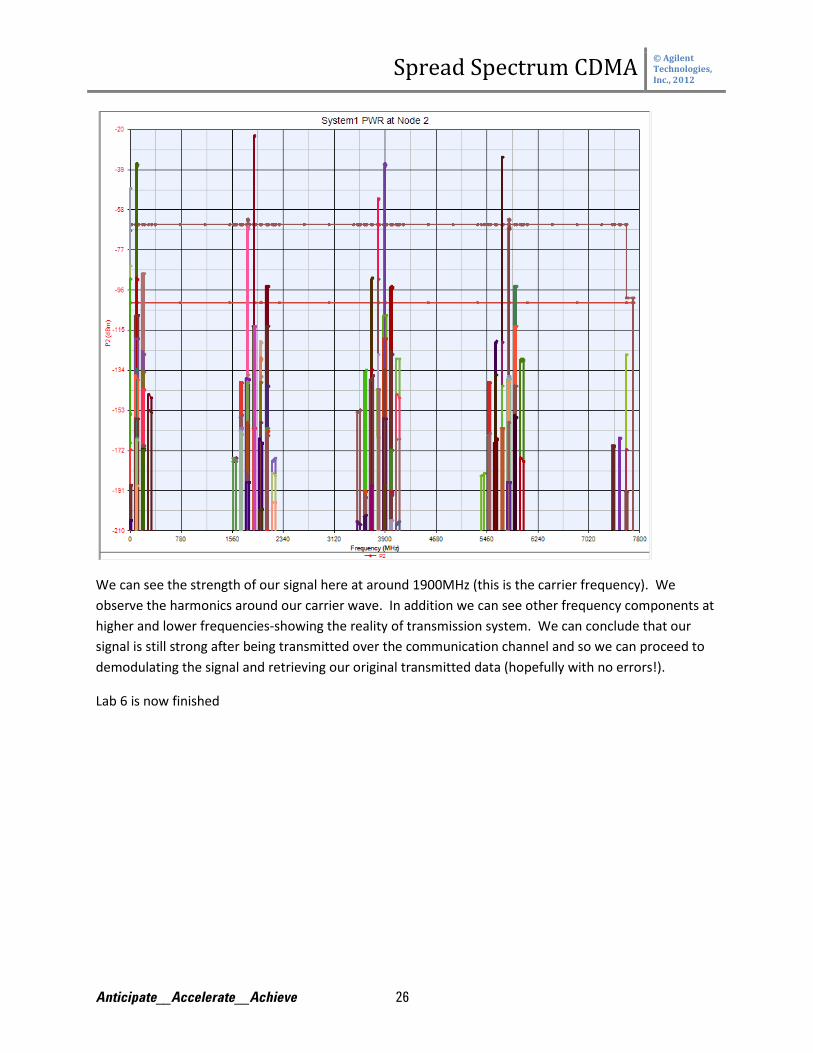
We can see the strength of our signal here at around 1900MHz (this is the carrier frequency). We observe the harmonics around our carrier wave. In addition we can see other frequency components at higher and lower frequencies-showing the reality of transmission system. We can conclude that our signal is still strong after being transmitted over the communication channel and so we can proceed to demodulating the signal and retrieving our original transmitted data (hopefully with no errors!).
Lab 6 is now finished

Spread Spectrum CDMA © Agilent Technologies, Inc., 2012
Anticipate__Accelerate__Achieve 27
7. Lab 7: Step7 Demodulation In this lab we will demodulate the signal and design the receiving side of the system.
1. Create a new folder called “Step7_Demodulation”> Add a new blank schematic and call it “Demodulation”> Add a data flow analysis and name it “DF_Demodulation”. Finally create a dataset called “DF1_Demodulation”.
2. Copy the design created in Step5_Modulation and paste the parts into the new blank schematic “Demodulation”.
3. In the workspace tree, expand the folder “Step6_RFLink”. Single click on the RFLink schematic and drag and drop (anywhere in the design) into the current “demodulation” schematic.
A neat part of SV is that new names can be edited to a name of your choice and can be joined without a physical wire-keeping your designs tidy and organised.
4. Click on the wire between “Noise density” and “Spectrum Analyzer”:
5. Right click on the wire> Net> Edit Net Name. Give the new name: “IF_in”
On the left hand side of the RF_Link, create a wire to allow us to pick the net and give it a name:

Spread Spectrum CDMA © Agilent Technologies, Inc., 2012
Anticipate__Accelerate__Achieve 28
Give it the wire the same name as the wire output from the noise density (“IF_in”). This will join the two parts together. Noise Density and the RF_Link are now connected.
6. Create a demodulation system (fundamentally this will be a mirror of the modulation system created).
7. Add a spectrum analyzer after the RF_Link (we will observe the power decrease following transmission). Copy the respective parts from Step5_Modulation as the parameters will have been saved too:
Math Lang model uses math language equations to process input data and produce output data. We can use this to ensure our sample rate is correct for demapping.
8. Double click on the math lang part and in the Equations tab copy the following:
Down sample by factor of 4
Call this sink “Rx_bits”
Call this sink “Tx_bits”
Add a delay of N=10. Output timing should be equaltoinput
Type into part selector “math”
“Demapper”
Walsh code at index 4
FCarrier=100MHz
Interpolation=4
Interpolation=1
Spread Spectrum CDMA © Agilent Technologies, Inc., 2012
Anticipate__Accelerate__Achieve 29
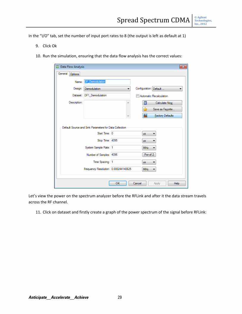
In the “I/O” tab, set the number of input port rates to 8 (the output is left as default at 1)
9. Click Ok
10. Run the simulation, ensuring that the data flow analysis has the correct values:
Let’s view the power on the spectrum analyzer before the RFLink and after it the data stream travels across the RF channel.
11. Click on dataset and firstly create a graph of the power spectrum of the signal before RFLink:

Spread Spectrum CDMA © Agilent Technologies, Inc., 2012
Anticipate__Accelerate__Achieve 30
12. Now let’s see the power spectrum after our data is streamed across the RF channel (After RFLink):

Spread Spectrum CDMA © Agilent Technologies, Inc., 2012
Anticipate__Accelerate__Achieve 31
We can see that the power before our data is modulated to a carrier that its power at 10MHz is around 1.18e-6W. After the signal is passed through the RFLink, the power is dropped to around 6.3e-9W. This power loss simulates real life conditions as the signal travels in air between the transmitting and receiving antenna and signal power maybe lost to trees, buildings and other general surroundings. We can also see the sidebands; it is safe to say that this will not affect our data at the receiving end as the Walsh code will reconstruct the information above the noise floor.
Now let’s see the individual bits and observe how good the transmission is.
13. In dataset, instead of producing a graph, conduct a table view of the transmitted bits and then compare with the received bits (Rx_bits and Tx_bits) N.B. Need step by step instructions? Refer back to Lab 3 where we produced a table to view our Walsh codes.

Spread Spectrum CDMA © Agilent Technologies, Inc., 2012
Anticipate__Accelerate__Achieve 32
We can conclude from the bits received that our system performs well.

Spread Spectrum CDMA © Agilent Technologies, Inc., 2012
Anticipate__Accelerate__Achieve 33
8. Lab8: Completed System In this lab we will calculate the BER to test its performance.
1. Add a new folder “Step8_CompletedSystem”, create a dataset DF1_CompletedSystem and a data flow analysis “DF_CompletedSystem”.
2. Copy the schematic created in Step 7 and paste it in the new blank schematic in Step8. Let’s cross correlate our two signals. This will allow us to compare the two signals and see the degree of similarity between them. In our CDMA system, it will compare the sent code and the saved code at the receiver (produced by our Walsh code generator). If the codes are similar then the receiver will decode it and produce the original transmitted signal.
3. In blank space within your schematic, add a cross correlator estimator Part Selector> type “cross” and select the cross correlator part.
4. Add two sinks, one at the delay (call it “Delay_Estimate”) and one called “Cross_Estimate” 5. Add a wire at each of the inputs and edit the names, call the y input “Test” and the x input “Ref”
(this can be achieved by double clicking on the wire and editing the default string)
6. Run the simulation 7. Plot the delay estimation graph as a cross correlation graph (Dataset>Delay_Estimate>New
Series Graph Wizard>Cross Correlation) 8. Now plot the cross estimation graph:

Spread Spectrum CDMA © Agilent Technologies, Inc., 2012
Anticipate__Accelerate__Achieve 34
We can imagine the transmitted signal and the signal saved at the receiver (by our Walsh code generator) slide over one another and as they the codes become increasingly matched, the cross correlation peaks forming a triangle like graph. And so the peak represents the offset, this is the point at which the codes are nearly perfectly matched. Let’s now test our performance by employing Bit Error Rate method. BER is used to measure the performance of a communication system as it is the rate at which errors occur in a transmission system. The BER is defines as
𝐵𝐸𝑅 = 𝑁𝑜. 𝑜𝑓 𝑏𝑖𝑡 𝑒𝑟𝑟𝑜𝑟𝑠
𝑇𝑜𝑡𝑎𝑙 𝑛𝑜. 𝑜𝑓 𝑏𝑖𝑡𝑠 𝑡𝑟𝑎𝑛𝑠𝑚𝑖𝑡𝑡𝑒𝑑
If the medium between the transmitted and receiving sides of a system is good then the signal to noise ratio will be high and the BER will be low. If a system has lots of noise, and coding techniques don’t math (in our case Walsh coding scheme) then the bits received differ greatly from the original transmitted bits and results in a high BER.
1. Choose a blank space within your schematic 2. Type “BER” into part selector and inject the relevant part into your design. The parameter
SampleStart on the BER_FER model should be set to 10 3. Add a delay of N=10 to the REF input terminal (this delay is added to ensure that the bit streams
are synchronised otherwise BER will be wrong). 4. Add wires at both inputs (so that we can name the wires). Connect the TEST input to our TEST
signal (this can be achieved by naming the wire “TEST”). Give the other wire at the REF input

Spread Spectrum CDMA © Agilent Technologies, Inc., 2012
Anticipate__Accelerate__Achieve 35
the name “REF”. This will allow the BER measurer to calculate the bit error rate of the transmitting signal and the end receiving signal (after Walsh code has decoded the signal):
Now let’s display our result in a text box.
5. Click on “Show/Hide Annotation Toolbar” situated in the top corner of the SV application:
A tool bar should appear, click on the square text box:

Spread Spectrum CDMA © Agilent Technologies, Inc., 2012
Anticipate__Accelerate__Achieve 36
Create two text boxes side by side (one displaying the value of our BER and the other can be the units or if you wish one text box displaying the value):
6. Double click on the text box on the right and in the text space key in “=BER”
Here you can change the position of the text, size, font, colour to suit your requirements.
7. Now double click on the text box on the left and in the text space type “BER (%)” After clicking ok, if your transmitting Walsh code generator index matches the Walsh code generator at the receiving end then you should have a 0% BER. This shows that our performance is perfect with all data transmitted have been successfully decoded by the Walsh code and received. Let’s change the index of one of our Walsh codes and see what happens
8. Click on one of the Walsh code generators and change the index to any number up to 8 (a different number to what is already set)

Spread Spectrum CDMA © Agilent Technologies, Inc., 2012
Anticipate__Accelerate__Achieve 37
9. Run the simulation Notice that your BER changes to above 0% (try changing the Walsh index once again and continue to run and observe the changes in the bit error rate). We have completed our CDMA Spread spectrum and tested its performance using BER in SystemVue software. As a final exercise, let’s use equations feature of SystemVue to observe the actual bits, Walsh codes and an alternative way to display BER. This uses math language equations to process output data.
1. In the workspace tree > Right Click on “tutorial” > Add > Add Equation Let’s make some example Walsh codes:
2. In the coding box (starting on line1), copy the following:
1 walsh1 = [ 1 -1 -1 1 1 -1 -1 1] %Write any comments here 2 walsh2 = [ 1 -1 -1 1 -1 1 1 -1] 3 walsh3 = [ 1 -1 -1 1 1 -1 -1 1]
N.B Notice that each Walsh code has equal numbers of 1s and -1s Notice the variables will be set on the left hand side tree.
3. Press Go to compile the code (this needs to be pressed after a new variable is created) 4. In the command window (bottom of screen), type any one of the Walsh code variables e.g.
Walsh1 (Please note that commands are case sensitive):
>> walsh1 ans = 1 -1 -1 1 1 -1 -1 1 >> Let’s now employ correlation techniques.
5. Auto correlate walsh1 6. Cross correlate walsh3 with walsh2
Observe the corresponding values via command window. Notice that autocorrelation produces a single entity of 1s-here we can prove that autocorrelation (which is the same as cross correlation with the
“%” enables you to write comments

Spread Spectrum CDMA © Agilent Technologies, Inc., 2012
Anticipate__Accelerate__Achieve 38
same code) will mean the data can be decoded and information can be retrieved (since there is a match). Cross correlating two different Walsh codes produces a mismatch as a series of 1s and -1s are created. Here there is a mismatch and the data cannot be decoded and so here we have seen and proved that the generator of Walsh code at the transmitting end must produce the same Walsh code at the receiving end in order to decode and obtain the original data. If we create a bit pattern, we can see what happens to our data as it is encrypted using Walsh code: Bits = [ 0 1 0 1 0 1 1 1] Walsh = [ 1 -1 -1 1 1 -1 -1 1] Answer = Bits.*Walsh Check the resultant array using the command box: >> Answer ans = 0 -1 -0 1 0 -1 -1 1 >> If we now take this coding and correlate it with our Walsh code (“Walsh”), we can retrieve our original bit pattern: Bits = [ 0 1 0 1 0 1 1 1] Walsh = [ 1 -1 -1 1 1 -1 -1 1] Answer = Bits.*Walsh Answer2 = Answer.*Walsh Check the resultant array using the command box: >> Answer ans = 0 1 0 1 0 1 1 1 >> Using the equations feature, we can view our BER result straight from the command window. Using this code: using(‘DF1_CompletedSystem’) BER = round(1e3*(B2_BER*100))/1e3 This will give us the BER as a percentage.

Spread Spectrum CDMA © Agilent Technologies, Inc., 2012
Anticipate__Accelerate__Achieve 39
9. Conclusion In conclusion, I hope you have enjoyed building a Spread Spectrum CDMA system and that you acquired all necessary tools to design, simulate, display and analyze results in various forms explored; Time plots, eye diagrams, spectra plots, power diagrams, frequency domain graphs and BER. I hope this has helped equip you to build more complex systems. SystemVue has an extensive library of examples, tutorial videos and web forums-all can be accessed via help menu. Also, we have other tutorial and workshop material to help you expose the benefit of using SystemVue for your design application, please refer to our EEsof homepage or contact us for more information, trials and licenses http://www.home.agilent.com/agilent/product.jspx?nid=-34360.0.00&lc=eng&cc=GB Thank you!

Spread Spectrum CDMA © Agilent Technologies, Inc., 2012
Anticipate__Accelerate__Achieve 40
10. Appendix 1
Here is some useful information and links to key areas discussed in this tutorial.
Agilent application note 1298 gives an introduction to digital modulation concepts and discusses different digital modulation types and gives an understanding of how digital transmitters and receivers work:
http://www.home.agilent.com/agilent/redirector.jspx?action=ref&cname=AGILENT_EDITORIAL&ckey=1817805&lc=eng&cc=GB&nfr=-11143.0.00&pselect=SR.GENERAL
By Divia Bhatnagar
For more information about SystemVue, please visit us on the web:
Product information http://www.agilent.com/find/eesof-systemvue Product Configurations http://www.agilent.com/find/eesof-systemvue-configs Request a 30-day Evaluation http://www.agilent.com/find/eesof-systemvue-evaluation Downloads http://www.agilent.com/find/eesof-systemvue-latest-downloads Helpful Videos http://www.agilent.com/find/eesof-systemvue-videos Technical Support Forum http://www.agilent.com/find/eesof-systemvue-forum
Copyright ©2012 Agilent Technologies. All rights reserved.