Embed Size (px)
Citation preview

SPIE PRESS Bellingham, Washington USA
SPIE PRESS

Library of Congress Cataloging-in-Publication Data
Names: Lin, Burn Jeng, 1942– author.Title: Optical lithography : here is why / Burn J. Lin.Description: Second edition. | Bellingham, Washington : SPIE, [2021] | Includesbibliographical references and index.
Identifiers: LCCN 2020049077 (print) | LCCN 2020049078 (ebook) | ISBN9781510639959 (hardcover) | ISBN 9781510639966 (pdf)
Subjects: LCSH: Microlithography. | Semiconductors–Etching. | Lasers–Industrialapplications.
Classification: LCC TK7872.M3 .L56 2021 (print) | LCC TK7872.M3 (ebook) |DDC 621.3815/31–dc22
LC record available at https://lccn.loc.gov/2020049077LC ebook record available at https://lccn.loc.gov/2020049078
Published bySPIEP.O. Box 10Bellingham, Washington 98227-0010 USAPhone: +1 360.676.3290Fax: +1 360.647.1445Email: [email protected]: www.spie.org
Copyright © 2021 Society of Photo-Optical Instrumentation Engineers (SPIE)
All rights reserved. No part of this publication may be reproduced or distributed inany form or by any means without written permission of the publisher.
The content of this book reflects the work and thought of the author. Every effort hasbeen made to publish reliable and accurate information herein, but the publisher isnot responsible for the validity of the information or for any outcomes resulting fromreliance thereon.
Printed in the United States of America.First Printing.For updates to this book, visit http://spie.org and type “PM329” in the search field.

Contents
Preface xv
1 Introduction 1
1.1 The Role of Lithography in Integrated Circuit Fabrication 21.2 The Goal of Lithography 41.3 The Metrics of Lithography 51.4 Introduction to the Contents of this Book 6
2 Proximity Printing 7
2.1 Introduction 72.2 Proximity Imaging 102.3 Region of Validity for Various Approximations of Diffraction 152.4 Proximity Images 232.5 E-G Diagram 312.6 Conclusion 36References 36
3 Exposure Systems 39
3.1 Projection Printing and a Comparison to Proximity Printing 403.2 Full-Wafer Field 433.3 Step and Repeat 473.4 Step and Scan 503.5 Reduction and 1X Systems 563.6 1X Mask Fabricated with a Reduction System 583.7 Summary 59References 59
4 Image Formation 61
4.1 The Aerial Image 614.1.1 Effects of a spherical wavefront and deviations from it 624.1.2 Spherical wavefront 624.1.3 The effect of a finite numerical aperture on the spherical
wavefront 654.1.4 Deviation from a spherical wavefront 71
4.1.4.1 The Seidel aberration coefficients 71
v
4.1.4.2 The Zernike polynomials 734.1.4.3 Sample plots of Zj 75
4.1.5 Imaging from a mask pattern 764.1.5.1 Coherent imaging from a mask pattern 774.1.5.2 Incoherent imaging from a mask pattern 814.1.5.3 Partially coherent imaging from a mask pattern 82
4.1.6 Spatial frequencies 844.1.6.1 Spatial frequencies of an isolated line opening 854.1.6.2 Spatial frequencies of line–space pairs 864.1.6.3 Angular spectrum 93
4.1.7 Imaging results 944.2 Reflected and Refracted Images 98
4.2.1 Methods to evaluate the reflected and refracted image froma mask 99
4.2.2 Impact of multiple reflections on DOF 1014.3 The Latent Image 1024.4 The Resist Image 103
4.4.1 The A, B, C coefficients 1074.4.2 The lumped parameters 1094.4.3 b and h 121
4.5 From Aerial Image to Resist Image 1244.6 The Transferred Image 125
4.6.1 Isotropic etching 1254.6.2 Anisotropic etching 1264.6.3 Lift off 1274.6.4 Ion implantation 1294.6.5 Electroplating 130
References 131
5 The Metrics of Lithography: Exposure-Defocus (E-D) Tools 135
5.1 The Resolution and DOF Scaling Equations 1355.2 Determination of k1 and k3 Based on Microscopy 1375.3 Determination of k1, k2, and k3 Based on Lithography 139
5.3.1 E-D branches, trees, and regions 1395.3.2 E-D window, DOF, and exposure latitude 1425.3.3 Determination of k1, k2, and k3 using E-D windows 144
5.4 k1, k2, and k3 as Normalized Lateral and Longitudinal Units ofDimension 145
5.5 The E-D Tools 1475.5.1 Construction of E-D trees 147
5.5.1.1 E-D tree construction from E-D matrixlinewidth data 147
5.5.1.2 E-D tree construction from E-D matrix edge data 1485.5.1.3 E-D tree construction from the intensity distribution 149
vi Contents
5.5.2 The importance of using log scale in the exposure axis 1515.5.3 Elliptical E-D window 1525.5.4 CD-centered E-D windows versus full-CD-range E-D windows 1545.5.5 E-D windows and CD control 1555.5.6 Application of E-D tools 156
5.5.6.1 Replacement of Bossung curves 1565.5.6.2 Combination of feature types 1595.5.6.3 Combination of feature sizes 1595.5.6.4 Combination of cuts for 2D features 1645.5.6.5 Combination of CD tolerances 1655.5.6.6 Combination of resist-processing tolerances 1655.5.6.7 Combination of image field positions 1695.5.6.8 Setting the mask-making tolerance 1705.5.6.9 Effects of phase-shifting mask errors 174
References 175
6 Hardware Components in Optical Lithography 177
6.1 Light Sources 1776.1.1 Mercury arc lamps 1776.1.2 Excimer lasers 180
6.1.2.1 Operation principle of the excimer laser 1806.1.2.2 Bandwidth narrowing 1816.1.2.3 Spatial coherence 1836.1.2.4 Maintenance, safety, and lifetime of excimer lasers 184
6.2 Illuminator 1856.2.1 Köhler illumination system 1856.2.2 Off-axis illumination 1866.2.3 Arbitrary illumination 187
6.3 Masks 1876.3.1 Mask substrate and absorber 1896.3.2 Pellicles 190
6.3.2.1 EUV pellicles 1906.3.3 Critical parameters for masks 191
6.3.3.1 CD control 1916.3.3.2 Placement accuracy 1916.3.3.3 Mask transmission and thermal expansion 1916.3.3.4 Mask reflectivity 1926.3.3.5 Mask flatness 1936.3.3.6 Physical size 1936.3.3.7 Defect level 194
6.3.4 Phase-shifting masks 1946.3.4.1 Operating principle 1946.3.4.2 An unflat BIM is not a PSM 196
viiContents
6.3.4.3 PSM types and their mechanisms for imagingimprovement 196
6.3.4.4 PSM Configurations 2006.4 Imaging Lens 203
6.4.1 Typical lens parameters 2036.4.1.1 Numerical aperture 2036.4.1.2 Field size 2046.4.1.3 Reduction ratio 2046.4.1.4 Working distance 2046.4.1.5 Telecentricity 205
6.4.2 Lens configurations 2056.4.2.1 Dioptric systems 2056.4.2.2 Reflective systems 2066.4.2.3 Catadioptric systems 207
6.4.3 Lens aberrations 2086.4.4 Lens fabrication 2096.4.5 Lens maintenance 210
6.5 Photoresists 2116.5.1 Classifications 211
6.5.1.1 Polarity 2126.5.1.2 Working principle 2136.5.1.3 Imaging configurations 221
6.5.2 Light interactions with a photoresist 2266.5.2.1 Wavelength compression 2266.5.2.2 Light absorption 2276.5.2.3 Resist bleaching or dyeing 2276.5.2.4 Resist outgassing 2276.5.2.5 Multiple reflections 228
6.5.3 Developed resist images 2336.5.3.1 Development of simple aerial images 2336.5.3.2 Development of diffracted aerial images 235
6.5.4 Antireflection coating (ARC) (by B.J. Lin and S.S. Yu) 2376.5.4.1 TE wave 2476.5.4.2 TM wave 248
6.6 Wafer 2486.7 Wafer Stage 2496.8 Alignment System 252
6.8.1 Off-axis alignment and through-the-lens alignment 2526.8.2 Field-by-field, global, and enhanced global alignment 2546.8.3 Bright-field and dark-field alignments 255
6.9 Conclusion 256References 256
viii Contents
7 Processing and Optimization 261
7.1 Optimization of the Exposure Tool 2617.1.1 Optimization of the NA 2617.1.2 Optimization of illumination 2657.1.3 Exposure and focus 2687.1.4 DOF budget 269
7.1.4.1 Components of DOFrequired 2707.1.4.2 Focus monitoring (by S.S. Yu) 274
7.1.5 Exposure tool throughput management 2797.2 Resist Processing 286
7.2.1 Resist coating 2867.2.1.1 Defects 2877.2.1.2 Resist adhesion 2877.2.1.3 Resist thickness 2887.2.1.4 Resist uniformity 2887.2.1.5 Conserving resist material 289
7.2.2 Resist baking 2917.2.2.1 Pre-coating bake 2927.2.2.2 Post-apply bake (pre-exposure bake) 2927.2.2.3 Post-exposure bake 2927.2.2.4 Hard bake 294
7.2.3 Resist developing 2967.2.4 Aspect ratio of the resist image 2987.2.5 Environmental contamination 301
7.3 k1 Reduction 3017.3.1 Phase-shifting masks 302
7.3.1.1 AltPSM 3027.3.1.2 AttPSM 310
7.3.2 Off-axis illumination 3147.3.2.1 Conceptual illustration 3147.3.2.2 Analysis of three-beam and two-beam images 316
7.3.2.2.1 Analysis of three-beam images 3167.3.2.2.2 Two OAI beams 3197.3.2.2.3 Two symmetrical beams 3207.3.2.2.4 Two asymmetrical beams due to non-
optimized pitches 3227.3.2.2.5 Combining two asymmetrical beams 3237.3.2.2.6 Numerical example of OAI in 1X and
reduction systems 3257.3.2.3 3D illumination on 2D geometry 3277.3.2.4 Simulation results 3297.3.2.5 Comparison of OAI and AltPSM 3367.3.2.6 Combination of OAI and AltPSM 336
ixContents
7.3.3 Scattering bars 3397.3.3.1 Imaging improvement from scattering bars 3397.3.3.2 Restricted pitch 3407.3.3.3 2D features 3427.3.3.4 Mask-making concerns 3427.3.3.5 Full-size scattering bar 3437.3.3.6 Hollow subresolution scattering bars and
subresolution assist PSMs 3437.3.4 Optical proximity correction 343
7.3.4.1 The proximity effect 3457.3.4.2 Edge corrections 3487.3.4.3 Edge correction by rule-based OPC 3497.3.4.4 Edge correction by model-based OPC 3497.3.4.5 Local-dosage OPC 3557.3.4.6 Full-depth OPC 3577.3.4.7 Correcting the after-etch image (AEI) 3597.3.4.8 Hot-spot checking 360
7.4 Polarized Illumination 3607.5 Multiple Patterning 361
7.5.1 Principle of the multiple-patterning technique (MPT) 3617.5.2 MPT processes 3667.5.3 MPT layouts 3687.5.4 G-rule for the double-patterning technique (DPT) 3697.5.5 Pack-unpack 3707.5.6 Resolution-doubling theory illustrated 3717.5.7 Overlay considerations of MPT 3737.5.8 Overcoming throughput penalty with double imaging 374
7.6 CD Uniformity (by S.S. Yu) 3767.6.1 CD nonuniformity (CDNU) analysis 377
7.6.1.1 Linear model for CDU contributions 3777.6.1.2 Geometrical decomposition 3777.6.1.3 Physical decomposition 3817.6.1.4 CDU summation 382
7.6.2 CDU improvement 3847.6.2.1 Active compensation with exposure tools 3847.6.2.2 Active compensation on tracks 384
7.7 Alignment and Overlay 3877.7.1 Alignment and overlay marks 3877.7.2 Using measured data for alignment 3897.7.3 Evaluation of interfield and intrafield overlay error
components 390References 394
x Contents
8 Immersion Lithography 399
8.1 Introduction 3998.2 Overview of Immersion Lithography 4008.3 Resolution and DOF 403
8.3.1 Wavelength reduction and spatial frequencies 4038.3.2 Resolution-scaling and DOF-scaling equations 4058.3.3 Improving resolution and DOF with an immersion system 4058.3.4 NA in immersion systems 406
8.4 DOF in Multilayered Media 4078.4.1 Transmission and reflection in multilayered media 4078.4.2 Effects of wafer defocus movements 4108.4.3 Diffraction DOF 4128.4.4 Required DOF 4138.4.5 Available DOF 4148.4.6 The preferred refractive index in the coupling medium 4158.4.7 Tradeoff between resolution and DOFdiffrac 417
8.5 Polarization in Optical Imaging 4188.5.1 Imaging with different polarizations 419
8.5.1.1 Recombination of spatial frequency vectors in theresist 419
8.5.1.2 Polarized refraction and reflection at the resistsurface 424
8.5.1.3 Different effects of polarized illumination 4268.5.2 Stray light 429
8.5.2.1 System stray light 4298.5.2.2 Stray light from recombination of spatial frequency
vectors inside the resist 4308.5.2.3 Stray light from reflection off the resist surface 4338.5.2.4 Incorporating polarization effects into E-D windows 4348.5.2.5 Simulation results with PDS 435
8.6 Immersion Systems and Components 4458.6.1 Configuration of an immersion system 4458.6.2 The immersion medium 4478.6.3 The immersion lens 4518.6.4 Bubbles in the immersion medium 4528.6.5 The mask 4568.6.6 Subwavelength 3D masks 4578.6.7 The photoresist 458
8.7 The Impact of Immersion Lithography on Technology 4608.7.1 Simulation of immersion lithography 4608.7.2 Poly layer 4628.7.3 Contact layer 466
xiContents
8.7.4 Metal layer 4688.7.5 Recommendation for the three technology nodes 470
8.8 Practicing Immersion Lithography 4718.8.1 Printing results 4728.8.2 Defect reduction 4728.8.3 Monitoring the immersion hood and special routing 4758.8.4 Other defect-reduction schemes 480
8.8.4.1 Wafer and equipment cleanliness 4818.8.4.2 Wafer seal ring 481
8.8.5 Results 4828.9 Extension of Immersion Lithography 484
8.9.1 High-refractive-index materials 4848.9.2 Solid-immersion masks 4858.9.3 Polarized illumination 4878.9.4 Multiple patterning 487
8.10 Conclusion 487References 488
9 EUV Lithography 493
9.1 Introduction 4939.2 EUV Source 497
9.2.1 Source power requirement 4979.2.2 The adopted LPP source 5019.2.3 Wall-power requirement of EUV systems 503
9.3 EUV Masks 5039.3.1 Configuration of EUV masks 5049.3.2 Effects of oblique incidence on the mask 505
9.3.2.1 Pattern shadowing 5059.3.2.2 Overlay and focusing errors from mask flatness 507
9.3.3 EUV mask fabrication 5109.3.4 EUV pellicles 512
9.4 Resolution-Enhancement Techniques for EUVL 5139.4.1 EUV flexible illumination 5149.4.2 EUV proximity correction 5169.4.3 EUV multiple patterning 5169.4.4 EUV phase-shifting masks 516
9.4.4.1 EUV AltPSM 5199.4.4.2 EUV AttPSM 521
9.5 EUV Projection Optics 5229.6 EUV Resists 524
9.6.1 Mechanism of EUV resist exposure 5259.6.2 CAR EUV resists 5259.6.3 Non-CAR EUV resists 527
xii Contents

9.7 Extendibility of EUVL 5319.7.1 Resist sensitivity, throughput, and power at each
technology node 5319.7.2 Increasing NA 534
9.8 Summary of EUVL 5359.9 Outlook of Lithography 536References 538
Appendix A: Methods to Evaluate the Region of Validity Based onLithography Applications 545
A.1 Motivation 545A.2 Similarity of the Approximation Methods According to the Pearson
Correlation Coefficient 545A.3 Critical Dimension 550A.4 Log-slope–CD Control 550A.5 Polychromatic Illumination 552A.6 Summary and Conclusion 556References 556
Index 557
xiiiContents
Preface to the Second Edition
The first edition of this book was published in 2010. Eleven years is a longtime in the field of lithography, even though much of the original content stillwithstands the passage of time and the advances in the technology nodes.Here are the reasons I decided to update this book:
1. Over these years, I am happy to have fulfilled my original goal ofmaking this book suitable for (1) newcomers to the field who areinteresting in growth into a technology career, (2) seasoned profes-sionals who seek more depth into the technology, and (3) managers andexecutives who seek more breadth. People from each of these groupshave told me that the book helped them and that they wouldrecommend it to new readers. With this new edition, I hope to makethe book even more useful.
2. For more than three years since my retirement from TSMC in Nov.2015, I have taught the course Innovative Lithography, using thematerials in this book. My students have given me the inspiration andenthusiasm to improve and update the book.
3. Lithography technology is fun to learn, fun to practice, and fun toteach. It is gratifying for me, once again, to preserve this knowledge ina book so that the torch can be passed.
This second edition features the following updates:Chapter 2 Proximity Printing. This is a completely new chapter. In
universities and many research labs, people need to make patterns with less-expensive equipment. Therefore, proximity printing is still very popular, eventhough there are not many publications on proximity imaging. I showrigorous and approximate ways to simulate the diffracted image at contactand in near, medium, and far fields, as well as the region of validity of thesemethods. The unintuitive positive- and negative-resist images from theproximity image are plotted. The E-G diagrams (from various authors) forquantifying proximity imaging are also covered. An appendix is provided todocument our (two of my graduate students’ and my) extensive research onmethods to determine the region of validity of the approximation methodsstudied.
xv
Chapter 3 Exposure Systems. To complement the coverage of historicaland current exposure systems for replicating patterns described in the firstedition, a carefully prepared step-by-step illustration of the mask and wafermovements in a step-and-scan system has been added. I also clarify that theprojection-printed image is a mirror image, despite the common impressionthat only proximity printing produces a mirror image.
Chapter 4 Image Formation. In addition to adding derivations of theresolution-scaling and DOF-scaling equations and analyses of spatialfrequency, light–resist interaction, and resist image development, I almostcompletely rewrote the section on Zernike polynomials, making their conceptseasier for lithography engineers to grasp. The simulated partially coherentimages in this chapter have been updated.
Chapter 5 E-D Methodology. This chapter is timeless. I provide adetailed explanation of how to construct E-D trees and emphasize why thelog scale is preferred for intensity and exposure. The term apparent exposure—the reciprocal of intensity—is introduced, and its use in E-D diagrams isexplained.
Chapter 6 Hardware Components. In this long chapter on lithographycomponents, I added examples of some enlightening resist developmentphenomena to help people visualize the resist development process. Thecoverage of chemically amplified resists is expanded. The coverage of wafers,the wafer stage, and alignment systems is also enriched.
Chapter 7 Processing and Optimization. This is another long chapter.I added new insightful derivations of off-axis illumination and a demonstra-tion of extracting the overlay error components with a redundant number ofdata points to improve the accuracy. Multiple patterning is also extensivelydiscussed, and the G-rule for double patterning is introduced.
Chapter 8 Immersion Lithography. This chapter continues the thoroughcoverage of this technology from the first edition with an outlook of itsextendibility and its impact on the semiconductor technology. The best scalingequations for resolution and DOF are given, and the numerical aperture ofthe reduction immersion system is clarified.
Chapter 9 EUV Lithography. I almost completely rewrote this chapter,which is quite understandable because of EUVL’s rapid growth during the lastdecade. Given that there are already other books on EUVL, I made sure thatmy contribution provides a valuable, unique perspective on the technology.
I omitted the material on MEB direct write to leave open the possibility ofproducing a single volume on this important topic for future development.Finally, I upgraded the figures with color for the eBook. Indeed, all of thefigures in the second edition have been modernized.
I credited my wife Sue for her support of the first edition and of my life ingeneral. Before starting my work on this revision, we celebrated our 50thanniversary in 2018. Sue continues to be an indispensable partner for her
xvi Preface to the Second Edition

support during my writing of this second edition and her support in myprofessional life, family life, and spiritual life.
Burn J. LinJuly 2021
xviiPreface to the Second Edition
Chapter 1
Introduction
Lithography creates a resist image on the wafer. The subsequent etching, liftoff, or ion implantation process is masked by the resist image at the areasdictated by the lithography mask. Hence, the thin-film material on the wafer isselectively removed or built up, or its characteristics are selectively altered.The resist image is produced by replicating the mask pattern, except in thecases of mask making or direct writing on the wafer. Figure 1.1 depicts themask replication process with an imaging lens. Light from the source iscollected by the condenser to illuminate the mask pattern. It passes throughthe imaging lens to form an aerial image that selectively exposes the resist.After development, the resist image as shown is produced. Figure 1.2illustrates various forms of image transfer from the resist to the underlyingthin film. The film can be isotropically or anisotropically etched, lifted off,plated, or implanted, using the patterned resist as the mask. Detaileddescriptions of these transfer processes are given in Chapter 4.
The image formation process is facilitated with an information-carryingbeam consisting of photons, electrons, or ions. Optical lithography usesphotons to carry out this process. Photons with energy ranging from visible tox-ray wavelengths can be used. However, in this book, the wavelengths ofconsideration are between 157 and 436 nm, as well as 13.5 nm. Thesewavelengths are already fully employed in manufacturing semiconductorintegrated circuits, except for 157 nm, which was forsaken after a lot ofheavily invested learning in research and development, and was replaced by193-nm water immersion, resulting in an equivalent wavelength of 134 nm.More details on 193-nm immersion lithography are given in Chapter 8.Chapter 9 covers the 13.5 nm extreme-UV (EUV) light that has started to beused for manufacturing 7-nm circuits.
The purpose of this book is to present the working principle of each areain optical lithography by providing examples instead of recipes on how to dothings. This way, readers understand why some techniques are used undercertain circumstance and why other techniques are not used. The aim is for
1
Chapter 2
Proximity Printing
2.1 Introduction
Soon after the integrated circuit (IC) was invented1 in 1958, lithography wasused to replicate the designed pattern on the mask to the wafer. The mostintuitive way to do so is to copy the mask pattern by direct contact of themask and the wafer. No lens is needed, the field size can be as large as themask, and the wafer does not even need to be precisely focused. Thisreplication technique was called contact printing, but this is a misnomer.Unless a deliberate effort is made to achieve intimate contact, the mask andthe wafer contact each other only at a few points over their entire area. Even ifintimate contact is achieved, because there is a photoresist layer between themask and the wafer, the mask is still in proximity to the wafer by the thicknessof the photoresist. In reality, intimate contact is not desirable for the followingthree reasons. (1) When the mask and the wafer are in intimate contact, high-contrast interference fringes will form wherever there are slight imperfectionsof contact, as shown in Fig. 2.1. These fringes make the contact exposurenonuniform. (2) The mask and the wafer become difficult to separate afterintimate contact. (3) Damage to the mask and the wafer is inevitable.Therefore, the proper lensless way to replicate a mask pattern is proximityprinting, not contact printing.
The proximity printing system consists of a light source, an illuminator, amask, a wafer, and a wafer stage that holds the wafer at a fixed distance fromthe mask, usually by putting spacers on the mask. Either the mask or thewafer is pressed hard against the other, with the spacers in between. The stagealso has the means to move the wafer with respect to the mask for alignmentpurposes; there are alignment-viewing devices to guide lateral positioning onthe wafer. A schematic of a proximity printing system is shown in Fig. 2.2.The system consists of illumination from the light source and the condenser.The mask and wafer are held in their respective holders to maintain a distanceon the order of 20 mm between the absorber surface of the mask and the resistsurface of the wafer. A larger distance prevents damage to the mask and thewafer; however, resolution is reduced rapidly as the mask-to-wafer gap
7
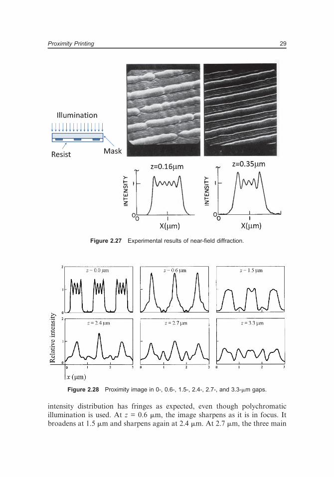
intensity distribution has fringes as expected, even though polychromaticillumination is used. At z = 0.6 mm, the image sharpens as it is in focus. Itbroadens at 1.5 mm and sharpens again at 2.4 mm. At 2.7 mm, the three main
Figure 2.27 Experimental results of near-field diffraction.
Figure 2.28 Proximity image in 0-, 0.6-, 1.5-, 2.4-, 2.7-, and 3.3-mm gaps.
29Proximity Printing
Chapter 3
Exposure Systems
Before getting into imaging theory and practice, I would like to presentexposure systems so that readers have the right perspective to approachChapters 4 and 5.
An exposure system reproduces the mask image at the wafer side toexpose the photoresist layer on a wafer. The reproduced image can be thesame size as the mask image in a 1X system. Reproduction on a modernexposure system usually reduces the reproduced image by a factor of 5 or 4,making it a 5X or 4X system, respectively. After development, this resistimage is used as an etch, implant, plating, or lift-off mask for pattern transferto a thin-film layer on the wafer.
There are different systems for reproduction. When the feature size was inthe 2- to 5-mm regime, and the budget for semiconductor manufacturing waslow, the aerial image in the 20- to 40-mm proximity of the mask sufficientlyproduced a useable resist image, maintaining feature size and placementcontrol as covered in Chapter 2.
Below 2 mm, infidelity of the aerial image, defect generation, andalignment viewing difficulties drove the bulk of exposure systems to 1X full-wafer projection printing. The 1X full-wafer coverage fills the requirement ofa smooth transition from proximity printing to projection printing.
When the minimum feature size of integrated circuits reached 1 mm, thefield size of full-wafer systems grew with the wafer size from 50 to 125 mm indiameter. This ever-increasing wafer size and reduced feature size—togetherwith the associated requirements of feature-size control and overlayaccuracy—drove exposure systems to reduction step-and-repeat. Reductionis used to addresses the need to resolve smaller features, tight feature-sizecontrol, and overlay accuracy. The step-and-repeat feature is used toaccommodate the ever-increasing wafer size in order to overcome the limitedimage field size of a projection system.
This chapter describes projection-printing systems, 1X and nX systems,and full-wafer, step-and-repeat, and step-and-scan systems. The significanceof reduction imaging is also analyzed.
39
Chapter 4
Image Formation
As discussed in Chapter 1, the goal of lithography is to place the edges of agiven mask pattern on the wafer within a specified tolerance. Doing so witheffective controls requires a good understanding of the image formationprocess—from the mask image to the final transferred image. The aerialimage is formed from the light that illuminates the mask and carries theinformation of the mask pattern through the lens to focus on the image plane.The aerial image becomes reflected and refracted as it propagates into theresist and is reflected and refracted numerous times by the resist, as well as bythe multiple film layers on the wafer substrate. The superposition of reflectedand refracted images in the resist exposes this medium, producing chemicaland physical changes. The distribution of these changes is the latent image.The exposed resist has a distribution of dissolution rate according to the latentimage. The developer removes the resist according to the dissolution ratedistribution and the topography of the resist surface. The developed resist isnow the resist image. The transferred image is dictated by the resist image andthe characteristics of the transfer process. These images are discussed below.
4.1 The Aerial Image
We define the aerial image as light distribution at the vicinity of the imageplane without any resist or multiply reflecting surface. The image must betreated as light waves in physical optics as opposed to light rays in geometricoptics. When the light wave has a perfect wavefront to form the image, there isno aberration to deteriorate the image. The only limit on resolution comesfrom the finite extent of the wavefront dictated by the aperture of the imaginglens. A larger aperture produces a better diffracted image. Such an imagingsystem is called a diffraction-limited system. We start our investigation using aperfect spherical wavefront with a finite lens aperture to form a point image,which leads to the relationship of diffraction-limited resolution to wavelengthand aperture size, followed by the relationship of depth of focus (DOF) to thesame set of parameters. Deviation from the spherical wavefront is treated in
61
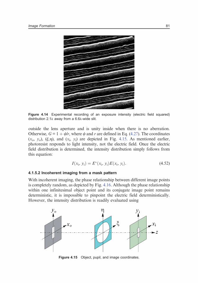
outside the lens aperture and is unity inside when there is no aberration.Otherwise, G = 1 þ c/r, where c and r are defined in Eq. (4.27). The coordinates(xo, yo), (j,h), and (xi, yi) are depicted in Fig. 4.15. As mentioned earlier,photoresist responds to light intensity, not the electric field. Once the electricfield distribution is determined, the intensity distribution simply follows fromthis equation:
Iðxi, yiÞ ¼ E�ðxi, yiÞEðxi, yiÞ: (4.52)
4.1.5.2 Incoherent imaging from a mask pattern
With incoherent imaging, the phase relationship between different image pointsis completely random, as depicted by Fig. 4.16. Although the phase relationshipwithin one infinitesimal object point and its conjugate image point remainsdeterministic, it is impossible to pinpoint the electric field deterministically.However, the intensity distribution is readily evaluated using
Figure 4.14 Experimental recording of an exposure intensity (electric field squared)distribution 2.1l away from a 6.6l-wide slit.
Figure 4.15 Object, pupil, and image coordinates.
81Image Formation

Chapter 5
The Metrics of Lithography:Exposure-Defocus (E-D) Tools
In microscopy, one is concerned with the closest distance between two objectsthat can be resolved in the image. The points of concern are quite different inlithography. A low-contrast image with a shallow intensity slope can beturned into a sharp edge with the photoresist. As mentioned in Section 1.3, thelocation of this edge is of prime interest and must be quantified against theoperating parameters of the exposure tool during manufacturing because itdetermines the feature size that may be related to circuit switching speed,leakage, resistance, etc. In addition, the edge position also determines whetherthe image in a given layer can be effectively overlaid with previous orsubsequent layers. The five primary parameters that can be adjusted in thefield are exposure dosage, focal position, pattern alignment between layers,magnification, and rotation. The last three parameters are mostly related tooverlay. Even though magnification can affect feature size in principle, itseffect on overlay is much greater than on feature size. The first twoparameters, exposure dosage and focal position, determine the processwindow of the lithographic system in a mutually dependent way. This mutualdependence and the ability to superimpose simultaneous requirements ondifferent features are captured in exposure-defocus (E-D) tools, which are thebackbone of lithography metrics.
5.1 The Resolution and DOF Scaling Equations
Section 3.2 introduced resolution and DOF scaling in projection printingusing the proportional relationship to wavelength and inversely proportionalrelationship to the lens numerical aperture without introducing theproportional constant. Equations (4.12) and (4.16) used an arbitrary constant0.5 to provide the physical meaning of these relationships. Here, we finallyintroduce the resolution and DOF scaling equation with rigorous propor-tional constants k1 and k3. The reason for the delay in presenting this equation
135
Chapter 6
Hardware Components inOptical Lithography
An optical lithography imaging system includes the following key compo-nents: a light source that provides the exposure photons with the desiredenergy spectrum; an illuminator that collects light from the source, adjusts itscoherence and incident angles, and delivers light to the mask uniformly; amask containing the circuit image to be replicated to the photoresist; animaging lens of the desired NA and field size to reproduce the mask image inthe resist by exposure; the resist layer coated on the wafer; the thin-film stackto be delineated by the pattern-transfer process or implantation; the waferheld by a chuck on a wafer stage that can be moved for alignment and fieldstepping; and alignment-viewing devices to guide the aligning movement ofthe stage. These components are described consecutively in the followingsections.
6.1 Light Sources
There are two types of light sources for use in optical lithography exposuretools: the mercury arc lamp and the excimer laser. These light sources arebright and efficient in their respective wavelength spectra.
6.1.1 Mercury arc lamps
The mercury arc lamp has been the light source of choice for opticallithography because of its many usable emission lines in the near-UV(350–460nm), mid-UV (280–350 nm), and deep-UV (200–280 nm) regions. There iseven an emission line at 184 nm. This lamp’s high brightness compared withother nonlaser sources is another reason for its popularity. Figure 6.1 showsthe radiation spectrum of a typical mercury arc lamp. Figure 6.2 shows aschematic drawing of a mercury arc lamp. Pointed and rounded electrodes areenclosed in a quartz envelope that contains a noble gas and a drop of mercury.During ignition, electric discharge takes place between the two electrodes. As
177
6.2 Illuminator
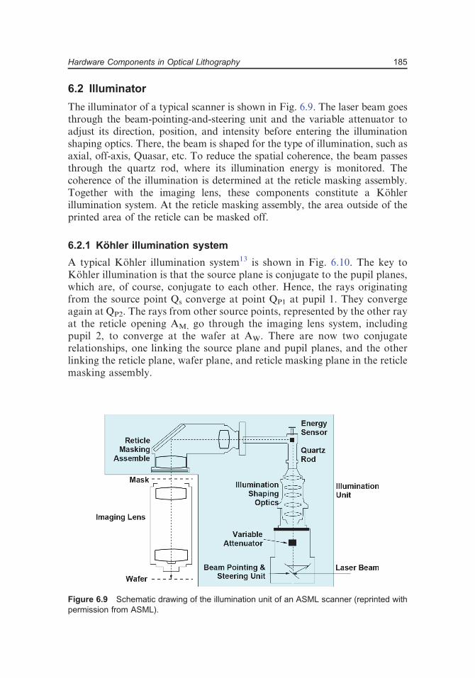
The illuminator of a typical scanner is shown in Fig. 6.9. The laser beam goesthrough the beam-pointing-and-steering unit and the variable attenuator toadjust its direction, position, and intensity before entering the illuminationshaping optics. There, the beam is shaped for the type of illumination, such asaxial, off-axis, Quasar, etc. To reduce the spatial coherence, the beam passesthrough the quartz rod, where its illumination energy is monitored. Thecoherence of the illumination is determined at the reticle masking assembly.Together with the imaging lens, these components constitute a Köhlerillumination system. At the reticle masking assembly, the area outside of theprinted area of the reticle can be masked off.
6.2.1 Köhler illumination system
A typical Köhler illumination system13 is shown in Fig. 6.10. The key toKöhler illumination is that the source plane is conjugate to the pupil planes,which are, of course, conjugate to each other. Hence, the rays originatingfrom the source point Qs converge at point QP1 at pupil 1. They convergeagain at QP2. The rays from other source points, represented by the other rayat the reticle opening AM, go through the imaging lens system, includingpupil 2, to converge at the wafer at AW. There are now two conjugaterelationships, one linking the source plane and pupil planes, and the otherlinking the reticle plane, wafer plane, and reticle masking plane in the reticlemasking assembly.
Figure 6.9 Schematic drawing of the illumination unit of an ASML scanner (reprinted withpermission from ASML).
185Hardware Components in Optical Lithography
Chapter 7
Processing and Optimization
Now that we have provided sufficient background on imaging and tools, theprocesses that use them and the optimization of these processes are given inthis chapter. We start with optimization of the exposure tools, then move onto resist processing, k1 reduction schemes, and finally the control of critical-dimension (CD) uniformity and overlay accuracy.
7.1 Optimization of the Exposure Tool
The optimization of an exposure tool involves the optimization of itsnumerical aperture (NA), illumination setting, exposure/focus, depth-of-focus(DOF) budget, and monitoring of focus, as well as its throughputoptimization in field size and exposure routing.
7.1.1 Optimization of the NA
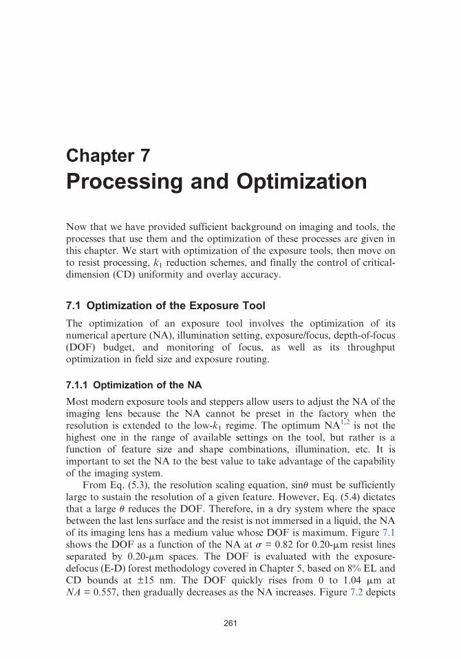
Most modern exposure tools and steppers allow users to adjust the NA of theimaging lens because the NA cannot be preset in the factory when theresolution is extended to the low-k1 regime. The optimum NA1,2 is not thehighest one in the range of available settings on the tool, but rather is afunction of feature size and shape combinations, illumination, etc. It isimportant to set the NA to the best value to take advantage of the capabilityof the imaging system.
From Eq. (5.3), the resolution scaling equation, sinu must be sufficientlylarge to sustain the resolution of a given feature. However, Eq. (5.4) dictatesthat a large u reduces the DOF. Therefore, in a dry system where the spacebetween the last lens surface and the resist is not immersed in a liquid, the NAof its imaging lens has a medium value whose DOF is maximum. Figure 7.1shows the DOF as a function of the NA at s = 0.82 for 0.20-mm resist linesseparated by 0.20-mm spaces. The DOF is evaluated with the exposure-defocus (E-D) forest methodology covered in Chapter 5, based on 8% EL andCD bounds at ±15 nm. The DOF quickly rises from 0 to 1.04 mm atNA = 0.557, then gradually decreases as the NA increases. Figure 7.2 depicts
261
7.3.4.8 Hot-spot checking
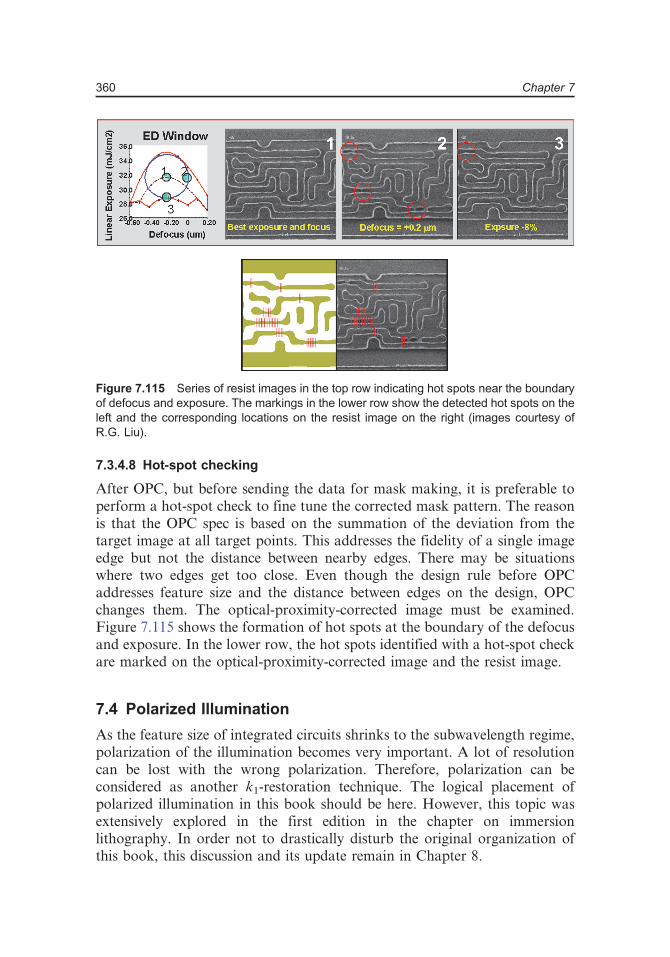
After OPC, but before sending the data for mask making, it is preferable toperform a hot-spot check to fine tune the corrected mask pattern. The reasonis that the OPC spec is based on the summation of the deviation from thetarget image at all target points. This addresses the fidelity of a single imageedge but not the distance between nearby edges. There may be situationswhere two edges get too close. Even though the design rule before OPCaddresses feature size and the distance between edges on the design, OPCchanges them. The optical-proximity-corrected image must be examined.Figure 7.115 shows the formation of hot spots at the boundary of the defocusand exposure. In the lower row, the hot spots identified with a hot-spot checkare marked on the optical-proximity-corrected image and the resist image.
7.4 Polarized Illumination
As the feature size of integrated circuits shrinks to the subwavelength regime,polarization of the illumination becomes very important. A lot of resolutioncan be lost with the wrong polarization. Therefore, polarization can beconsidered as another k1-restoration technique. The logical placement ofpolarized illumination in this book should be here. However, this topic wasextensively explored in the first edition in the chapter on immersionlithography. In order not to drastically disturb the original organization ofthis book, this discussion and its update remain in Chapter 8.
Figure 7.115 Series of resist images in the top row indicating hot spots near the boundaryof defocus and exposure. The markings in the lower row show the detected hot spots on theleft and the corresponding locations on the resist image on the right (images courtesy ofR.G. Liu).
360 Chapter 7
Chapter 8
Immersion Lithography
8.1 Introduction
Immersion lithography is a dark horse. The International TechnologyRoadmap for Semiconductors (ITRS)—documents adopted by all equipmentand material suppliers—together with semiconductor manufacturing compa-nies reduced the actinic wavelength from 436 nm to 365 nm, 248 nm, 193 nm,157 nm, then 13.4 nm. The 436- and 365-nm wavelengths are two prominentlines produced by the mercury arc lamp. The 248-, 193-, and 157-nmwavelengths are generated by XeCl, KrF, and F2 excimer lasers, respectively,followed by 13.4-nm EUV light, initially generated by Xe plasma, and thenenhanced by switching to Sn plasma.
The ITRS continued to be followed over the years. Just before the year2000, 193-nm lithography was projected to reach its limit with the 0.93-NAimaging optics, which can handle the 65-nm node and stretched to the 55-nmhalf node. However, following the roadmap, the industry started working ondeveloping 157-nm lithography much earlier than year 2000.
Unfortunately, only CaF2 is suitable for lens material at such a shortwavelength. This material has been used in 193-nm applications, but thespecification is much more stringent for 157 nm. A heavy investment wasmade to grow a large, perfect CaF2 crystal for the imaging lens, but thisattempt was not successful. A major reason for the failure is the 90-dayturnaround time required to grow the large crystal. As many as 600 crystal-growing furnaces have been employed to develop the CaF2 productionprocess, but to no avail.
Developing a resist for 157 nm also faced tough challenges. Until theworldwide termination of the 157-nm program, no satisfactory resist had beendemonstrated. The pellicle material was also wanting. No suitable membranematerial was available. The only option was to use quartz or CaF2 as a thickpellicle. Then, mounting and demounting the pellicle without affecting theoptical performance of the imaging system became a difficult problem. Lastly,oxygen absorbs 157-nm light, so the optical path must be in nitrogen, makingthe system inconvenient and hazardous to operate. Even though nitrogen is
399
8.6.3 The immersion lens
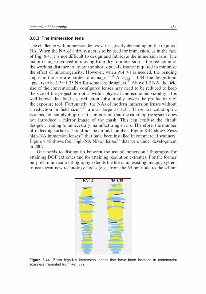
The challenge with immersion lenses varies greatly depending on the requiredNA. When the NA of a dry system is to be used for immersion, as in the caseof Fig. 8.4, it is not difficult to design and fabricate the immersion lens. Themajor change involved in moving from dry to immersion is the reduction ofthe working distance to utilize the short optical distance required to minimizethe effect of inhomogeneity. However, when NA >1 is needed, the bendingangles in the lens are harder to manage.30,31 At nCM = 1.44, the design limitappears to be 1.3 ~ 1.35 NA for some lens designers.35 Above 1.2 NA, the fieldsize of the conventionally configured lenses may need to be reduced to keepthe size of the projection optics within physical and economic viability. It iswell known that field size reduction substantially lowers the productivity ofthe exposure tool. Fortunately, the NAs of modern immersion lenses withouta reduction in field size36,37 are as large as 1.35. These are catadioptricsystems, not simply dioptric. It is important that the catadioptric system doesnot introduce a mirror image of the mask. This can confuse the circuitdesigner, leading to unnecessary manufacturing errors. Therefore, the numberof reflecting surfaces should not be an odd number. Figure 8.44 shows Zeisshigh-NA immersion lenses38 that have been installed in commercial scanners.Figure 8.45 shows four high-NA Nikon lenses39 that were under developmentin 2007.
One needs to distinguish between the use of immersion lithography forattaining DOF extremes and for attaining resolution extremes. For the formerpurpose, immersion lithography extends the life of an existing imaging systemto near-term new technology nodes (e.g., from the 65-nm node to the 45-nm
Figure 8.44 Zeiss high-NA immersion lenses that have been installed in commercialscanners (reprinted from Ref. 38).
451Immersion Lithography

Chapter 9
EUV Lithography
9.1 Introduction
Optical lithography in the regime of k1¼ 0.28 is very complicated. The imagecontrast is low and, except for 1D single-pitch patterns with specialilluminations, the mask error enhancement factor (MEEF) is high. Forcontact hole patterning, the MEEF can be more than 4, which negates thegain of a 4X reduction system. Line ends can have MEEF as high as 10. Inaddition, the shape of patterns at low k1 is rounded out and requires asignificant amount of optical proximity correction to keep the patterns usable.Extreme-UV lithography1,2 (EUVL) previously used the 13.4-nm wavelength.Recently, this technology migrated to 13.5 nm. Either wavelength offers anorder of magnitude reduction in wavelength from the water-immersion ArFwavelength of 134 nm. This presents an opportunity to bring k1 back to above0.5. It is no wonder that EUV lithography has attracted large research anddevelopment efforts worldwide. The size of the EUV development effort hasdwarfed two other well-known lithography developments, namely, 157-nmlithography and x-ray proximity printing. Take the 32-nm half pitch. At thewater-immersion ArF wavelength of 134 nm and sinu¼ 0.95, k1 is 0.227.Turning to EUV at sinu¼ 0.25, k1 becomes 0.597. Initially, the term softx-ray3 was used to identify this lithography. However, the use of UV light hashad an impressive history of success compared to x-ray lithography. It makessense to associate the technology with the winning wavelength range, thus it iscalled EUV lithography. Since the publication of Ref. 1 in 1989, more than threedecades have passed and many challenges have been met. EUVL for productionof the 7-nm node has been demonstrated.4 High-volume manufacturing isexpected to follow. It will be worthwhile to track the number of nodes by whichthe three decades of development efforts can extend semiconductor scaling.
With such a dramatic drop in wavelength, the imaging system issubstantially different from existing systems. First, EUV light is heavilyabsorbed by any substance, including gases. The optical path must be invacuum. Second, because of EUV light’s strong absorption characteristics, thereis no transmitting material—EUV optical imaging depends on reflection.
493
slot field is taken from a large circular field, as in a scanner lens. The imagequality should be uniformly good. Even after taking aberrations intoconsideration, the uniformity of the imaging quality of such a slot fieldshould still be much better than that from a slit field.*
The illuminator used in the ASML EUV alpha tool is shown in Fig. 9.5.The collector reflects the EUV light at the IF such that the light goes throughthe illuminator optics (consisting of two normal-incidence mirrors and twograzing-incidence mirrors) to reach the mask. This simplified illuminator isused here to show a typical number of mirrors in an illumination system.Production-type illuminators that need to enable OAI, source optimization,and source mask optimization, as well as to control the partial coherence, aremuch more complicated, just like the DUV illuminator. Examples of someilluminators can be found in Section 5.5.3 of Ref. 19.
9.2 EUV Source
The EUV source has been a key bottleneck of EUVL for high-volumemanufacturing; the power level has been insufficient to support a viablethroughput. After an enormous investment of billions of dollars by suppliersand potential users that involved the research of thousands of individuals,engineering prowess combining talents in many disciplines, management andmarketing skills, will power, and vision, the EUV source can now support anacceptable but not exciting throughput. The path to further increasing thesource power is now visible, but this high power brings additional challengingproblems concerning power grid loading, heat removal, and environmentalimpact. Before discussing the working principle of the source, let’s firstconsider the source power requirements and impacts. Because there is nooptical layout of the illuminator, we use the number of collectors and mirrorsin the illumination module of the alpha tool.54
9.2.1 Source power requirement
An EUV scanner needs to be economical for manufacturing semiconductors.It is anticipated that the scanner itself will cost many times more than a 193-nm immersion scanner. The space required for the EUV source is also manytimes larger. The raw power required and the consumables such as water andgases are in much larger quantities. Therefore, to avoid cost escalation, it isvery important to make the throughput of EUV scanners much higher thanthat of conventional scanners. This means economically increasing the sourcepower and transmission of the optical system, overcoming the limits in scanspeeds, or increasing the resist sensitivity.
*In a step-and-scan exposure tool, we use “slit” to denote a curved field and “slot” for astraight field.
497EUV Lithography
Burn J. Lin is a Distinguished Research Chair Professor atthe National Tsing Hua University in Taiwan and theDirector of the Tsing Hua-TSMC Joint Research Center.From 2011 to 2015 he was Vice President and a Distin-guished Fellow at TSMC, Ltd., which he joined in 2000 as aSenior Director. Earlier he held various technical andmanagerial positions at IBM in the U.S., after joining theIBM T.J. Watson Research Center in 1970. He has been
extending the limit of optical lithography for half a century. In 1991, hefounded Linnovation, Inc. and is still the CEO of the company.
Dr. Lin is the inaugurating Editor in Chief of the Journal of Micro/Nanolithography, MEMS, and MOEMS, a life member of the U.S. NationalAcademy of Engineering, Academician of Academia Sinica, Laureate of theIndustrial Technology Research Institute in Taiwan, IEEE and SPIE LifeFellow, and a joint distinguished professor at the National Chiao TungUniversity and the National Taiwan University. He is also DistinguishedAlumni of the Ohio State University and the National Taiwan University.
Dr. Lin is the recipient of the 2018 Future Science Prize in Mathematicsand Computer Science, a 2017 SPIE Award for inaugurating the OpticalMicrolithography Conference in 1987, the 2013 IEEE Jun-Ichi NishizawaMedal, the first Semi IC Outstanding Achievement Award in 2010, the 2009IEEE Cledo Brunetti Award, the 2009 Benjamin G. Lamme MeritoriousAchievement Medal, the 2007 Industrial Technology Advancement Award,the 2006 Distinguished Optical Engineering Award from the OpticalEngineering Society of R.O.C., the 2005 Most Valuable Player in VLSIResearch Inc.’s All-Stars of the Chip Making Industry, the 2005 Two BestR&D Managers in Taiwan, the 2004 Outstanding Research Award fromPWY Foundation, the first SPIE Fritz Zernike Award in 2004, the 2003Outstanding Scientific and Technological Worker Award, and the 2002 TenBest Engineers in Taiwan award. Throughout his career, he has received 2TSMC Innovation Awards, 10 IBM Invention Awards, and an IBMOutstanding Technical Contribution Award.
Dr. Lin has been pioneering deep-UV lithography since 1975, multilayerresist systems since 1979, simulation of 2D partially coherent imaging since1980, exposure-defocus methodology since 1980, scaling equations ofresolution and depth of focus since 1986, k1 reduction since 1987, proofs of1X mask limitations since 1987, vibration in optical imaging since 1989,electrical measurement of contact holes since 1989, E-G tree for x-rayproximity printing since 1990, experimental demonstration of the impact ofmask reflectivity on imaging since 1990, optimum lens NA since 1990,attenuated phase-shifting mask since 1991, signamization since 1996, LWD-hand LWD-b since 1999, nonparaxial scaling equations of resolution and depthof focus since 2000, 193-nm immersion lithography since 2002, and

polarization-induced stray light since 2004. His innovations and researchefforts have spanned 21 lithography generations, starting at the 5000-nm nodeand extending to the 5-nm node.
Dr. Lin has written 2 books, 3 book chapters, and more than 132 articles,71 of which he is the sole or the first author. He also holds 88 U.S. patents.