Embed Size (px)
Citation preview

IEEE P802.3bm, July 2013, Geneva Specification for 100GBASE-DR4 1
Specification for 100GBASE-DR4
Piers Dawe
IEEE P802.3bm, July 2013, Geneva

IEEE P802.3bm, July 2013, Geneva Specification for 100GBASE-DR4 2
Supporters
Arlon Martin Kotura
IEEE P802.3bm, July 2013, Geneva Specification for 100GBASE-DR4 3
Introduction
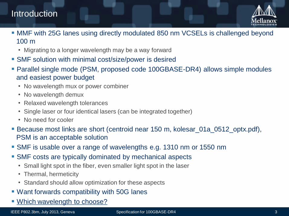
MMF with 25G lanes using directly modulated 850 nm VCSELs is challenged beyond
100 m
• Migrating to a longer wavelength may be a way forward
SMF solution with minimal cost/size/power is desired
Parallel single mode (PSM, proposed code 100GBASE-DR4) allows simple modules
and easiest power budget
• No wavelength mux or power combiner
• No wavelength demux
• Relaxed wavelength tolerances
• Single laser or four identical lasers (can be integrated together)
• No need for cooler
Because most links are short (centroid near 150 m, kolesar_01a_0512_optx.pdf),
PSM is an acceptable solution
SMF is usable over a range of wavelengths e.g. 1310 nm or 1550 nm
SMF costs are typically dominated by mechanical aspects
• Small light spot in the fiber, even smaller light spot in the laser
• Thermal, hermeticity
• Standard should allow optimization for these aspects
Want forwards compatibility with 50G lanes
Which wavelength to choose?

IEEE P802.3bm, July 2013, Geneva Specification for 100GBASE-DR4 4
Discussion 1
Transmitter could be directly modulated lasers or laser(s) + optical modulator
The same photodiodes can receive at both 1310 nm and 1550 nm
If directly modulated, performance for 25G lanes over temperature is better at 1310
nm than 1550 nm
• But for other transmitter types, it's different – see later
Direct modulation is challenging for 25G lanes, looks extremely challenging for 40G
or 50G lanes
If optical modulator,
• See next slide

IEEE P802.3bm, July 2013, Geneva Specification for 100GBASE-DR4 5
Discussion 2
If optical modulator, • Wider range of technology options at 1550 nm (C band):
- 1 III-V with glass lensing
- 2 III-V with waveguides on silicon (hybrid integration)
2a Out of plane coupling e.g. gratings
2b Edge coupling e.g. butt coupling
- 3 SiGe modulators with glass lensing
- 4 SiGe modulators with waveguides on silicon (hybrid integration)
4a Out of plane coupling e.g. gratings
4b Edge coupling e.g. butt coupling
- 5 III-V with III-V lensing
• Optical modulation has the potential for 40G or 50G lanes
• Some Out of Plane coupling methods are wavelength selective
• Fewer technology options at 1310 nm (O band): - 1 III-V with glass lensing
- 2 III-V with waveguides on silicon (hybrid integration)
2a Out of Plane coupling e.g. gratings
2b Edge coupling e.g. butt coupling
- 3 SiGe modulators with glass lensing
- 4 SiGe modulators with waveguides on silicon (monolithic integration)
4a Out of plane coupling e.g. gratings
4b Edge coupling e.g. butt coupling
- 5 III-V with III-V lensing
The more traditional technologies (e.g. option 1) are appropriate for a small, moderate or uncertain market volume • Lower NRE
Silicon photonics becomes interesting for a large volume • Higher NRE
Simpler kinds of silicon photonics are appropriate for cost reasons (e.g. option 4b)
<- Technology
restrictions or
uncertainties

IEEE P802.3bm, July 2013, Geneva Specification for 100GBASE-DR4 6
Recommendation
A wide range of technologies should be allowed to enable a broad market and
lower cost
Both 1310 nm and 1550 nm transmitters should be allowed
While 1310 nm (O band) has served 802.3 for direct modulation, as we cost-optimise
with optical modulation we should be in the 1550 nm (C) band
Consequences for interoperability:
Photodiode has to work at both 1310 nm and 1550 nm
Not a significant problem; such photodiodes have been made for many years
• Photodiodes respond to photons, not optical power. The optical power that delivers a
particular photocurrent can be lower at 1530 nm than at 1310 nm
- May be a concern for overload
Receiver input coupling has to work at both 1310 nm and 1550 nm

IEEE P802.3bm, July 2013, Geneva Specification for 100GBASE-DR4 7
1530 1535 1540 1545 1550-8
-7
-6
-5
-4
-3
-2
-1
0
wavelength (nm)
OM
A m
in (
dB
m)
For maximum TDP
For TDP <= 0.8 dB
1530 1535 1540 1545 1550-12
-10
-8
-6
-4
-2
0
wavelength (nm)
Rece
ive
r se
nsitiv
ity
OM
A m
ax (
dB
m)
Recommendation – detail 1
1295 1300 1305 1310 1315 1320 1325-8
-7
-6
-5
-4
-3
-2
-1
0
wavelength (nm)
OM
A m
in (
dB
m)
For maximum TDP
For TDP <= 0.8 dB
1295 1300 1305 1310 1315 1320 1325-12
-10
-8
-6
-4
-2
0
wavelength (nm)
Rece
ive
r se
nsitiv
ity
OM
A m
ax (
dB
m)
O band
O band
C band
C band
Figure 96–3—Transmitter minimum OMA
Figure 96–4—Receiver sensitivity
In P802d3bm-96_PSM4_01.pdf
96.7.1 100GBASE-?R4 transmitter optical specifications • Table 96–6—100GBASE-?R4 transmit characteristics
• Change
• Lane wavelength (range) 1295 to 1325 nm
• to
• Lane wavelength (range) 1295 to 1325 or 1530 to 1550 nm
96.7.1.1 Transmitter OMA, each lane (min) • Add 1550 nm option: change
• "Tx_OMA >= MAX(-8.65+((lambda-1310)^2)/100, -8.05) + MAX(TDP, 0.8) dBm"
• to
• "Tx_OMA >= {MAX(-8.65+((lambda-1310)^2)/100, -8.05) + MAX(TDP, 0.8) dBm
• or
• Tx_OMA >={MAX(-8.65+((lambda-1540)^2)/138.2, -8.05) + MAX(TDP, 0.8) dBm"
96.7.2 100GBASE-?R4 receive optical specifications • Table 96–7—100GBASE-?R4 receive characteristics
• Change
• Lane wavelengths (range) 1295 to 1325 nm
• to
• Lane wavelength (range) 1295 to 1325 and 1530 to 1550 nm
96.7.2.1 Receiver sensitivity (OMA), each lane (max) • Add 1550 nm option: change
• "Rx_sens <= MAX(-11.89 + ((lambda–1310)^2)/100, -11.4) dBm"
• to
• "Rx_sens <= MAX(-11.89 + ((lambda–1310)^2)/100, -11.4) dBm
• or
• Rx_sens <= MAX(-11.89 + ((lambda–1540)^2)/138.2, -11.4) dBm"

IEEE P802.3bm, July 2013, Geneva Specification for 100GBASE-DR4 8
Recommendation – detail 2
96.7.3 100GBASE-?R4 illustrative link
power budget
Table 96–8—100GBASE-?R4
illustrative link power budget
• No changes needed
96.8.5.2 Channel requirements
• See next slide
96.10 Fiber optic cabling model
• See table to right
Description Value
O band
C band Unit
Operating distance (max) 500 m
Channel insertion lossa, b(max) 3.26 3.26 dB
Channel insertion loss (min) 0 dB
Positive dispersionb (max) 1.2 9.1 ps/nm
Negative dispersionb (min) –1.4 8.5 ps/nm
DGD_maxc TBD ps
Optical return loss (min) TBD dB
Table 96–13—Fiber optic cabling (channel) characteristics for 100GBASE-?R4
aThese channel insertion loss values include cable, connectors, and
splices. bOver the wavelength range 1295 nm to 1325 nm of Table 96–6. cDifferential Group Delay (DGD) is the time difference at reception
between the fractions of a pulse that were transmitted in the two
principal states of polarization of an optical signal. DGD_max is the
maximum differential group delay that the system must tolerate.

IEEE P802.3bm, July 2013, Geneva Specification for 100GBASE-DR4 9
Recommendation – detail 3
96.8.5.2 Channel requirements
PMD type
Wavelength range
Dispersiona (ps/nm) Insertion
lossb
Optical
return
lossc
Max
mean
DGD
Minimum Maximum
100GBASE-?R4
O band
0.011625×λ×[1–(1324 / λ)4] 0.011625×λ×[1–(1300 / λ)4]
Minimum
TBD dB
TBD ps
C band 0 (maximum) aThe dispersion is measured for the wavelength of the device under test (λ in nm). The coefficient assumes 500 m
for 100GBASE-?R4. bThere is no intent to stress the sensitivity of the BERT’s optical receiver. cThe optical return loss is applied at TP2.
Table 96–11—Transmitter compliance channel specifications

IEEE P802.3bm, July 2013, Geneva Specification for 100GBASE-DR4 10
If overload is a concern
If overload is a concern,
96.7.1 100GBASE-?R4 transmitter optical specifications • Table 96–6—100GBASE-?R4 transmit characteristics
• Change
• Total average launch power (max) 8 dBm
• to
• Total average launch power (max) 8 7.5 dBm
• Change
• Average launch power, each lane (max) 2 dBm
• to
• Average launch power, each lane (max) 2 1.5 dBm
• Change
• Optical Modulation Amplitude (OMA), each lane (max) 2.2 dBm
• to
• Optical Modulation Amplitude (OMA), each lane (max) 2.2 1.7 dBm
96.7.2 100GBASE-?R4 receive optical specifications • Table 96–7—100GBASE-?R4 receive characteristics
• Change
• Average receive power, each lane (max) 2 dBm
• to
• Average receive power, each lane (max) 2 1.5 dBm
• Change
• Receive power, each lane (OMA) (max) 2.2 dBm
• to
• Receive power, each lane (OMA) (max) 2.2 1.7 dBm

IEEE P802.3bm, July 2013, Geneva Specification for 100GBASE-DR4 11
Other changes proposed
1. 96.7.1 100GBASE-?R4 transmitter optical specifications
• Table 96–6—100GBASE-?R4 transmit characteristics
• Extinction ratio spec can be relaxed: OMA and TDP (which includes optical return loss
tolerance) provide the necessary protection. 100GBASE-SR4 has 3 dB
• Change Extinction ratio (min) from 3.5 to 3 dB
2. 96.7.2 100GBASE-?R4 receive optical specifications
• Table 96–7—100GBASE-?R4 receive characteristics
• The MDI connector is an angled type, so Receiver reflectance (max) –12 dB is not necessary
• Change Receiver reflectance (max) from –12 to –20 dB
• In Table 96–6—100GBASE-?R4 transmit characteristics, adjust Optical return loss tolerance
(max), presently 7.94 dB, appropriately
• In Table 96–11—Transmitter compliance channel specifications, for Optical return loss,
change TBD to the modified Optical return loss tolerance (max) from Table 96–6
3. Delete erroneous entry:
• Receiver 3 dB electrical upper cutoff frequency, each lane (max) 12.3 GHz

IEEE P802.3bm, July 2013, Geneva Specification for 100GBASE-DR4 12
Conclusions
Allowing both 1310 and 1550 nm transmitters broadens the market for
100GBASE-DR4
• It also lays the foundations for 40G or 50G lanes
Adopt P802d3bm-96_PSM4_01.pdf with the changes shown on slides 7, 8, 9, 10 and
11

IEEE P802.3bm, July 2013, Geneva Specification for 100GBASE-DR4 13
Silicon Photonics and wavelength
Silicon is transparent at SMF
wavelengths and enables low
loss optical devices
Ge absorbs at SMF
wavelengths to enable
detection
Ge is CMOS compatible
Working at 1.55 μm (band
edge of Ge) enables the use
of SiGe compounds for
efficient modulation
• Where the absorption curve is
steep
GeSi
Applied
voltage

IEEE P802.3bm, July 2013, Geneva Specification for 100GBASE-DR4 14
Wavelength options and WDM
Highly scalable: many WDM
channels available, vision of a path
to 1 Tb/s and beyond
Components, test equipment and
so on are available for a range of
wavelengths
Enables innovative technical
solutions: • Silicon photonics
• III/C PICS
Best for Si
Photonics

IEEE P802.3bm, July 2013, Geneva Specification for 100GBASE-DR4 15
Thank You