Embed Size (px)
Citation preview

REPORT OF DEPARTMENT OF DEFENSE
ADVISORY GROUP ON ELECTRON DEVICES
SPECIAL TECHNOLOGY AREA REVIEW ON
Field Programmable Gate Arrays (FPGAs) for Military Applications
July 2005
OFFICE OF THE UNDER SECRETARY OF DEFENSE ACQUISITION, TECHNOLOGY & LOGISTICS
WASHINGTON, DC 20301-3140
THIS REPORT IS A PRODUCT OF THE DEFENSE ADVISORY GROUP ON ELECTRON DEVICES (AGED). THE AGED IS A FEDERAL ADVISORY COMMITTEE ESTABLISHED TO PROMOTE INDEPENDENT ADVICE TO THE OFFICE OF THE DIRECTOR OF DEFENSE AND ENGINEERING. STATEMENTS, OPINIONS, RECOMMENDATIONS, AND CONCLUSIONS IN THIS REPORT DO NOT NECESSARILY REPRESENT THE OFFICIAL POSITION OF THE DEPARTMENT OF DEFENSE.

Report Documentation Page Form ApprovedOMB No. 0704-0188
Public reporting burden for the collection of information is estimated to average 1 hour per response, including the time for reviewing instructions, searching existing data sources, gathering andmaintaining the data needed, and completing and reviewing the collection of information. Send comments regarding this burden estimate or any other aspect of this collection of information,including suggestions for reducing this burden, to Washington Headquarters Services, Directorate for Information Operations and Reports, 1215 Jefferson Davis Highway, Suite 1204, ArlingtonVA 22202-4302. Respondents should be aware that notwithstanding any other provision of law, no person shall be subject to a penalty for failing to comply with a collection of information if itdoes not display a currently valid OMB control number.
1. REPORT DATE JUL 2005
2. REPORT TYPE N/A
3. DATES COVERED -
4. TITLE AND SUBTITLE Special Technology Area Review on Field Programmable Gate Arrays(FPGAs) For Military Applications
5a. CONTRACT NUMBER
5b. GRANT NUMBER
5c. PROGRAM ELEMENT NUMBER
6. AUTHOR(S) 5d. PROJECT NUMBER
5e. TASK NUMBER
5f. WORK UNIT NUMBER
7. PERFORMING ORGANIZATION NAME(S) AND ADDRESS(ES) Office of the Under Secretary of Defense Acquisition and TechnologyWashington, DC 20301-3140
8. PERFORMING ORGANIZATIONREPORT NUMBER
9. SPONSORING/MONITORING AGENCY NAME(S) AND ADDRESS(ES) 10. SPONSOR/MONITOR’S ACRONYM(S)
11. SPONSOR/MONITOR’S REPORT NUMBER(S)
12. DISTRIBUTION/AVAILABILITY STATEMENT Approved for public release, distribution unlimited
13. SUPPLEMENTARY NOTES
14. ABSTRACT
15. SUBJECT TERMS
16. SECURITY CLASSIFICATION OF: 17. LIMITATION OF ABSTRACT
SAR
18. NUMBEROF PAGES
62
19a. NAME OFRESPONSIBLE PERSON
a. REPORT unclassified
b. ABSTRACT unclassified
c. THIS PAGE unclassified
Standard Form 298 (Rev. 8-98) Prescribed by ANSI Std Z39-18

ii
CLEARED For Open Publication
AUG 23 2005 3
Office of Freedom of Information
And Security Review Department Of Defense

iii
FOREWORD The Advisory Group on Electron Devices (AGED) is chartered by the Department of Defense (DoD) Instruction 5129.39 and functions according to the DoD Directive 5105.4 Federal Advisory Committee Management Program. The AGED provides advice to the Director of Defense Research and Engineering in the area of electronic and photonic device technologies. The AGED conducts Special Technology Area Reviews (STARs) to assess the status and potential benefits of advanced electronic and photonic technologies for defense applications. Topics with Terms of Reference (TOR) for the STARs are solicited from elements of the Department and approved by the Deputy Undersecretary of Defense (Science and Technology). The findings and recommendations of the AGED STAR activity are reported to the Director of Defense Research and Engineering. This STAR on Field Programmable Gate Arrays (FPGAs) for Military Applications was conducted on August 3-4, 2004 at the Naval Postgraduate School in Monterey, California. Its objective was to provide information that will assist the DoD in defining and pursuing a defense-wide application strategy for the use of FPGAs in present and future military information, computer, and sensor systems.
FPGAs are rapidly becoming an essential flexible integrated circuit building block of
choice for many commercial and defense systems. As their performance, complexity, cost, and capacity have improved, these devices have begun to challenge the use of Application Specific Integrated Circuits (ASICs) in many electronic systems. In some applications the ability to incorporate built-in core functionality such as those of microprocessors or digital signal processing (DSPs) has lead to preferred system level solutions over traditional design approaches. Military systems, however, differ from their commercial counterparts in terms of their production volume, radiation tolerance, assured secure functionality, and system lifetimes.
The STAR examined two crucial elements of FPGA technology: 1) component technologies and 2) FPGA microsystem application design tools and methodologies. The status of FPGA technologies was assessed in terms of capabilities, cost, risk, implementation (including design), security, and performance vis-à-vis alternative technologies such as ASICs. On behalf of the AGED, I express my sincere appreciation to all of the people who took part in this study − listed in the following section − for their valuable contributions. I thank particularly Dr. Gerald M. Borsuk, the Co-Chair of the FPGA STAR Committee, for doing so much to assure a successful workshop. I extend my thanks and appreciation to Dr. Charles Byvik, ODDR&E/S&T/SS, whose support and encouragement were essential for the successful completion of this effort. In addition, I thank the members of the STAR Committee, Dr. Carter Armstrong, Mr. Zach Lemnios, Dr. Les Palkuti, Dr. Dan Radack, Ms. Joan Pierre, Dr. Rick Ridgley, Dr. Linda Katehi, and the former AGED Executive Secretariat, Mr. Eric Carr and Mr. David Cox, and commended them for significant contributions to this study. Their expertise helped immensely in the preparation of this report. Dr. Matthew Goodman Advisory Group on Electron Devices

iv
This Page Intentionally Left Blank

v
CONTRIBUTORS
Dr. Matthew S. Goodman** Special Government Employee (SGE)
and Telcordia Technologies STAR Chair
Dr. Gerald M. Borsuk**
Naval Research Laboratory STAR Co-Chair
Dr. Thomas Albano
DoD Dr. Carter Armstrong**
SGE & L-3 Communications Dr. Tom Banwell
Telcordia
Mr. John Bloomfield Mercury Computer
Mr. Regan Branstetter Raytheon
Mr. Richard Calatayud Northrop Grumman
Dr. Charles Cerny Air Force Research
Laboratory
Mr. Chris Clardy Actel
Mr. Lew Cohn DTRA
Dr. Charles Cox* SGE & Photonic Systems
Mr. Brian Cronquist Actel
Dr. Erik Daniel Mayo Clinic
Mr. Amr El-Ashmawi Altera
Mr. Richard Elmhurst Honeywell
Mr. Michael Enoch Lockheed Martin
Mr. John Fagan Atmel
Mr. Brian Faith QuickLogic
Mr. Dan Gardner Mentor Graphics
Mr. Matt Gariepy Lattice Semiconductor
Dr. Tom Hart QuickLogic
Dr. Alfred Hung Army Research Laboratory
Ms. Kay Jobe Boeing
Dr. Rick Jones DTSA
Dr. Linda Katehi* SGE & Purdue University
Mr. Tim Kemerley* Air Force Research
Laboratory
Dr. Fouad Kiamilev University of Delaware
Dr. Ken LaBel NASA
Mr. Zach Lemnios* DARPA
Mr. Henry Livingston BAE Systems
Mr. Marc Lovend DoD
Dr. Jim Lyke Air Force Research
Laboratory
Mr. Dan Mansur Mentor Graphics
Mr. John McCollum Actel

vi
Mr. Ken O’Neill Actel
Mr. Rick Padovani Xilinx
Dr. Les Palkuti** DTRA
Dr. Don Parker* DTRA
Dr. John Pellegrino* Army Research Laboratory
Mrs. Joan Ma Pierre** DTRA
Dr. Dan Radack** DARPA
Mr. Jeremy Ramos Honeywell
Dr. Rick Ridgley** DoD
Dr. Ted Roberts Naval Research Laboratory
Dr. Kaushik Roy Purdue University
Mr. Ted Speers Actel
Mr. Steve Stark Lattice Semiconductor
Mr. Pat Stover Annapolis Microsystems
Dr. Randy Sylvester L-3 Communications
Dr. Michael Vai MIT Lincoln Labs
Dr. Bob Wisnieff* SGE & IBM
** AGED STAR Committee members * AGED members

TABLE OF CONTENTS
FOREWORD ................................................................................................................................. iii CONTRIBUTORS.......................................................................................................................... v TABLE OF CONTENTS.............................................................................................................. vii TABLE OF FIGURES................................................................................................................. viii Executive Summary ........................................................................................................................ 1 Introduction, Purpose, and Scope ................................................................................................... 3 Background and FPGA Technology History.................................................................................. 8 Synopsis of Government Sessions ................................................................................................ 10 Synopsis of Vendor Presentations ................................................................................................ 12 Synopsis of Academia Session ..................................................................................................... 15 Synopsis of OEMs Session ........................................................................................................... 17 Synopsis of Design and Software Session.................................................................................... 19 Synopsis of Defense Industry Sessions ........................................................................................ 21 Synopsis of Rad-Hard Presentations............................................................................................. 29 Future Vision for FPGA Technologies ......................................................................................... 33 Observations, Findings and Recommendations............................................................................ 41 Further DoD Implications of the S&T Recommendations ........................................................... 45 Summary and Conclusions ........................................................................................................... 46 APPENDIX A – STAR AGENDA............................................................................................... 47 APPENDIX B – TERMS OF REFERENCE................................................................................ 49 APPENDIX C – QUESTIONS FOR PANELISTS ...................................................................... 51 APPENDIX D – ACRONYM GLOSSARY ................................................................................ 53
viii
TABLE OF FIGURES
Figure 1. FPGAs - Where They Fit................................................................................................. 5 Figure 2. Area Efficiency versus Computational Efficiency.......................................................... 5 Figure 3. Most Common Methods of Implementing System Designs............................................ 6 Figure 4. COTS FPGA Boards, Custom FPGA Boards, and Conceptual FPGA Architecture ...... 6 Figure 5. Cost of Developing ASIC’s - a Driver for the Move to FPGAs ..................................... 7 Figure 6. FPGA, Cell-based ASIC and Structured ASIC Development Costs.............................. 7 Figure 7. Available and Planned radiation tolerant FPGA devices ............................................. 11 Figure 8. FPGA processors: Example of soft and hard cores ....................................................... 14 Figure 9. Tradeoffs for system design: FPGAs vs ASICs ............................................................ 16 Figure 10. Impact of high-level design tools on FPGA design .................................................... 20 Figure 11. Systems Application Interface Design ........................................................................ 20 Figure 12. Technology Application Domains............................................................................... 22 Figure 13. Military Contractors’ View of Comparative Technology Strengths of FPGAs versus
ASICs.................................................................................................................................... 26 Figure 14. Examples of trade-offs in critical parameters; ASICs and FPGAs for a space-based
system ................................................................................................................................... 26 Figure 15. RHOC survey of determined needs for advanced rad hard FPGA requirements....... 30 Figure 16. FPGA hardening projects planned on the RHOC roadmap (May 04). ....................... 31 Figure 17. Near-term and long-term projection of technology nodes .......................................... 34 Figure 18. Number of transistors per chip .................................................................................... 35 Figure 19. On-chip clock frequency ............................................................................................. 35 Figure 20. ASIC usable devices per cm2...................................................................................... 36 Figure 21. Interdependency of S&T Areas on FPGA Applications ............................................. 43

1
Executive Summary
The Advisory Group on Electron Devices (AGED) held a Special Technology Area Review (STAR) on Field Programmable Gate Arrays (FPGAs) for Military Applications on August 3-4, 2004 at the Naval Postgraduate School in Monterey, California to address issues relevant to the use of this technology in military systems. FPGAs are rapidly becoming an essential flexible integrated circuit building block of choice for many commercial and defense systems. The STAR confirmed that FPGAs are a crucial electronic component in many DoD electronic systems and are likely to be for some time. However, the STAR also uncovered several areas of concern that AGED believes should be addressed by the DoD. Many of these concerns are due to the inherent differences between the rapidly expanding commercial market for FPGAs (>15% per year growth rate) that is geared to rapid product obsolescence and the military market that is geared to performance assurance and long product life cycles. An overwhelming majority of the FPGA business is commercial in nature (>90%) limiting the leverage of the DoD to influence the direction of its development. The STAR covered all major aspects of FPGAs for military use. A key area of concern is that the reliability of FPGAs is poorly understood leading to unexpected system vulnerabilities and failures. The STAR concluded:
1. Immature FPGA technology has been incorporated into military systems with significant impact on cost and schedule. Vendor deployment of new products is driven by the expectation of their rapid obsolescence inherent in the commercial marketplace.
2. Vendor specific software design platforms are immature, not well integrated, and not interoperable among different vendors. Even though programmable logic arrays have existed for over twenty years, a lack of common definitions, standards and benchmarking for performance and capacity hinder technology tradeoffs amongst vendors and point to the immaturity of the technology. The traditional role FPGAs have played as “glue chips” in electronic systems has changed as their complexity and functionality has increased in recent years.
3. Design, validation, testing, verification and feedback is lacking from primary vendors but is available to some degree from 3rd party vendors.
4. Hardware and software products performance and features touted by the vendors was not confirmed by the military systems user community.
5. Security concerns are of a very low priority to the vendor community and that security vulnerabilities are poorly understood by the military equipment manufacturing community. Fabless FPGA vendors (who outsource the actual manufacturing of their products) have limited control and auditing capability over the manufacturing and process control of their products leading to security and reliability vulnerabilities. Technology challenges unique to FPGAs exist include for example: the scalability of 6-transistor static random access memories (SRAM) cell much beyond the 90 nm generation; the need for architectural and circuit innovations to improve power dissipation per unit area; the need for floating point arithmetic Intellectual Property (IP) cores (not generally available on FPGAs); and mixed signal cores are also lacking.
2
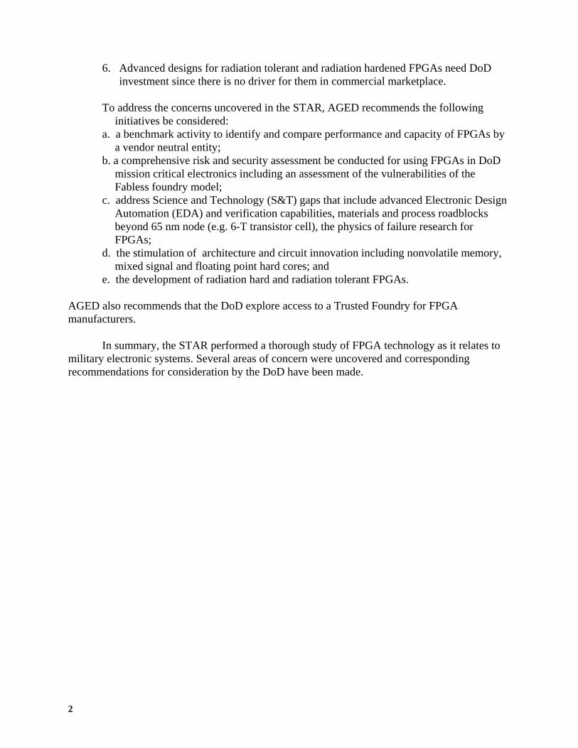
6. Advanced designs for radiation tolerant and radiation hardened FPGAs need DoD investment since there is no driver for them in commercial marketplace.
To address the concerns uncovered in the STAR, AGED recommends the following
initiatives be considered: a. a benchmark activity to identify and compare performance and capacity of FPGAs by
a vendor neutral entity; b. a comprehensive risk and security assessment be conducted for using FPGAs in DoD
mission critical electronics including an assessment of the vulnerabilities of the Fabless foundry model;
c. address Science and Technology (S&T) gaps that include advanced Electronic Design Automation (EDA) and verification capabilities, materials and process roadblocks beyond 65 nm node (e.g. 6-T transistor cell), the physics of failure research for FPGAs;
d. the stimulation of architecture and circuit innovation including nonvolatile memory, mixed signal and floating point hard cores; and
e. the development of radiation hard and radiation tolerant FPGAs. AGED also recommends that the DoD explore access to a Trusted Foundry for FPGA manufacturers.
In summary, the STAR performed a thorough study of FPGA technology as it relates to
military electronic systems. Several areas of concern were uncovered and corresponding recommendations for consideration by the DoD have been made.

3
Introduction, Purpose, and Scope In response to a request from OSD, AGED has evaluated FPGA technology for military applications using the STAR process. This STAR had a diverse set of goals and objectives. The high level objectives were: 1. Assess the state-of-the-art in FPGAs and establish the likely technology development
roadmap; 2. Quantify the systems level benefits of using FPGAs for defense systems; 3. Identify the technology issues that if solved, will lead to significant advancement; 4. Identify the potential risks and vulnerabilities due to the deployment of FPGAs in military
systems; 5. Identify defense unique requirements that impact the development of this technology; 6. Determine what supporting technologies are required to realize the benefits of FPGAs; and 7. Assess the potential for assuring secure electronics for military applications.
The Terms of Reference were established and are included as Appendix B. A STAR workshop was held August 3-4, 2004 at the Naval Postgraduate School in Monterey, CA for the purpose of discussing these issues. Approximately 60 people attended the STAR workshop. The government was represented by OSD, the Army, Navy and Air Force research laboratories, DARPA, DTRA, MDA, the intelligence community (NSA and NRO), and NASA. Seven of these Agencies provided direct input with presentations at the STAR workshop (See Appendix A). The FPGA industry was represented at the STAR workshop by representatives from all the major manufacturers of FPGAs, including Xilinx, Altera, Actel, Atmel, Lattice Semiconductor and QuickLogic corporations. These companies represent nearly all the manufacturing of FPGAs in the world. There were presentations by representatives of two original equipment manufacturers (OEMs); Annapolis Microcomputer and Mercury Computer. These two electronic subsystem vendors provide the industry with generic subsystems level solutions based on FPGAs. The STAR received input from the research community including presentations by professors at the University of Delaware and Purdue University schools of engineering and a representative of the High Performance Electronics Group from the Mayo Clinic. After the STAR workshop, the STAR committee interviewed representatives from the Los Alamos National Lab and representatives from MIT Lincoln Labs to obtain their views on FPGA technology. A number of military contractors who use FPGAs to build military systems provided presentations to provide the users’ perspective. The military contractors represented included Honeywell, Northrop-Grumman, L-3 Communications, Raytheon Corporation, BAE Systems, Lockheed Martin, and Boeing. These presentations provided perspectives of the FPGA solutions, on why FPGAs are used given the implementation difficulties and types of unforeseen problems that are part of the current state of the art of the FPGA technology.

4
Attendees were asked to provide input on specific questions that were provided to the attendees in advance of the STAR workshop. Questions of particular interest that speakers were asked to comment on are: • How will FPGAs develop in terms of capability and gate counts relative to other
technologies (e.g., ASICs)? • How effective are the FPGA gate counts relative to other technologies? • What are the near- and long-term limits to this technology? • Is there foreign ownership of the “IP Cores” within the FPGAs and what fraction of the IP is
foreign owned? • Do the FPGA vendors view DoD as their customers, and if not, why not? • Can the FPGA products meet unique DoD requirements including radiation hard, military
temperature requirements, etc? • What are the barriers to inserting FPGA technology into military applications and where
might they fit best? • What are the cost and affordability metrics? • Are there materials, reliability or manufacturing problems? • Are there design or software issues? • What is the vision for this technology?
The STAR wrestled with the difficulties of comparing ASIC gate counts to FPGA gate counts with a special open evening session devoted largely to a frank discussion of this issue. An overview of the FPGA’s place in to the various families of electronic logic is shown in Figure 1. These logic families can be divided into two main groups, standard electronic logic and ASICs. ASICs can further be subdivided into programmable logic devices, gate arrays, cell based ICs and full custom ICs. The primary difference is that of programmability versus regular structures (e.g. RAM). The programmable logic devices can be divided into three main categories depending on the degree of programmability. FPGAs performance compared to ASICs performance is shown in Figure 2. The fraction of commercial systems designs incorporating various different logic technologies is illustrated in Figure 3. An FPGA is an array of configurable logic blocks, memory blocks, arithmetic blocks and interconnection systems, which can be programmed by the designer (see Figure 4). FPGAs can be divided into three categories: one-time programmable devices, which are programmed at hardware “burn-in” of the logic structure; non-volatile reprogrammable based on flash memories or EPROMs; and volatile reprogrammable based on SRAM technologies. While the STAR focused on FPGAs, many of the observations, findings and recommendations apply to other forms of programmable electronic logic as well.

5
0.1
1
10
100
1000
0.01 0.1 1 10 100 1000
Computational Efficiency (GOPS/Watt)
Area
Effi
cien
cy (G
OPS
/cm
2 )
ASIC
FPGA
DSP
Figure 5 and Figure 6 show the dramatic cost increase of the non-recurring costs for ASIC development (arguably a very conservative estimate). FPGAs are applied in 3 primary ways – for prototyping of a variety of real-time systems and for systems development, for ASIC prototyping, and for direct use or ASIC replacement. Of these three, by far the most prevalent in commercial practice is the third, while in DoD and military systems the most prevalent use is the first two application types.
Figure 1. FPGAs - Where They Fit
Figure 2. Area Efficiency versus Computational Efficiency

6
Figure 3. Most Common Methods of Implementing System Designs
(Source: EE Times, Industrial Survey)
Figure 4. COTS FPGA Boards, Custom FPGA Boards, and Conceptual FPGA
Architecture
(Source: M. Vai, MIT Lincoln Laboratory)
36 %
6 %
14 %
14 %
32 %
0 10 20 30 40
Percentages
Cell-based ASICs
Large “off the shelf”ICs (or ASSPs)
Structured orplatform ASIC
Combination or other
FPGAs
36 %
6 %
14 %
14 %
32 %
0 10 20 30 40
Percentages
Cell-based ASICs
Large “off the shelf”ICs (or ASSPs)
Structured orplatform ASIC
Combination or other
FPGAs

7
Figure 5. Cost of Developing ASIC’s - a Driver for the Move to FPGAs
(Source: M. Vai, MIT Lincoln Laboratory)
able 1 - Comparing Total Costs of doing in 1M gate designs in 0.13um Note: Prorated Unit Cost = Per piece cost + (Qty/Total Design Cost) FPGA Structured ASIC Cell Based ASIC Total Design Cost: ~$165K ~ $500K ~ $5.5M (Typical) Vendor NRE: None ~ $100K - $200K $1M to $3M # Tools Required: 2 to 3 2 to 3 6 to 10 Cost of Tools: ~ $30K ~ $120K to $250K > $300K # Engineers: 1 to 2 2 to 3 5 to 7 Price per chip: $220 to $1K ~ $30 to $150 ~ $30 Unit Cost (Qty 1K): ~ $1000 ('03) $500 to $650 $ 55K Unit Cost (Qty 5K): ~ $220 (4Q'04) $100 to $150 $1.1K Unit Cost: (Qty 500K): ~ $40 (4Q'04) > $21 $11 to $20 Figure 6. FPGA, Cell-based ASIC and Structured ASIC Development Costs

8
Background and FPGA Technology History Since their invention in 1984, Programmable Logic Devices (PLDs) have grown from a few hundred gates to close to ten million gates. The predominant programmable element today is the FPGA. Furthermore, instead of sea of gates, FPGAs today can include built-in hardwired processors, memory, multiplier accumulators, standard cells, clock management systems, and other building blocks. In other words, FPGAs can be configured as system on a chip (SoC). Today, worldwide market for FPGAs is approaching $3 billion. The advantages of programmable devices such as FPGAs as compared to fixed logic devices such as ASICs include the time to production and the cost effectiveness. By comparison, with ASIC chips, the time-to-design, prototype, and manufacture can take months to longer than a year. Furthermore simulation, design verification, testing, and performance validation can take a substantial effort. The cost of complex ASIC chips, including engineering design, computer aided design tools, photolithography mask sets, prototyping, and eventually manufacturing, can be millions of dollars (see Figure 5 and Figure 6). FPGAs, as its name indicates, are standard off the shelf parts that can be programmed to perform specific functions on the fly. Except for the programming, the gates and cells and building blocks have all been fully validated. Thus SoC designers can quickly develop, simulate, and test their designs using widely available design and development tools. Final SoC demonstration is much quicker and cost much less than ASIC parts. The drawback with FPGAs, in general, is that the design is mostly limited to digital logic devices. If the SoC design requires integration with analog devices, analog phase lock loops, Micro-Electro-Mechanical Systems (MEMS) devices, Radio Frequency (RF) devices, optical devices such as infrared (IR), and other functions, then ASICs are still necessary. Even within the area of digital logic, if the design requires uniquely specific logic functions such as high performance Reduced Instruction Set Computer core processors, a custom designed ASIC is still required. Building blocks in FPGAs are limited to the standard set of processing core functions such as adders and multiplier accumulators and registers as well as blocks of SRAM. In terms of computational speed or clock frequency, FPGAs are usually much slower due to the non-optimal layout of the interconnects. Clock rates in FPGAs are in the hundreds of MHz, whereas ASICs for the same device geometry can run in the GHz. Still for many military and civilian applications, such as Digital Signal Processing (DSP), the performance of PLDs is adequate. Generally there are two types of programmable logic devices, complex programmable logic devices (CPLD) and FPGA. Some of the PLDs can be programmed only once, and some can be reprogrammed repeatedly. Of the two types, FPGAs offer the highest logic gate density and the highest performance, as well as the most building block features. Between the two extremes of fully FPGA’s and custom designed chips, there are hybrids for specific applications. Currently there are six major manufacturer of FPGAs: Xilinx, Altera, Actel, Atmel, QuickLogic and Lattice Semiconductor. Of these, Xilinx is the leader in FPGA technology with over 50% of the market share. With its flexibility, reprogrammability, and substantial lower cost as compared to custom designed ASICs, it is not surprising that increasingly large numbers of FPGAs are being deployed in military systems. Military application of FPGAs presents unique problems, one of

9
the foremost is the need for security of the information on the chip and susceptibility to reverse engineering. Reverse engineering (RE) of the programs in the FPGA by competitors in the civilian sector is not a significant problem, but is a more serious problem for military parts. If a weapon system is captured by the adversary, RE of the part can render the weapon system ineffective. There are FPGAs that can make RE difficult if not impossible, such as the anti-fuse one time programmable technology. Protection of the programmed function in the FPGA remains a serious problem for the military.

10
Synopsis of Government Sessions
Requirements Overview DoD designers traditionally used small gate count FPGAs as glue logic to interface with discrete integrated digital circuits. Designers later turned to custom ASICs to reduce parts count, production cost, and enhance performance. More recently, FPGA gate counts have reached 6-10 million with enhanced clock speed while the non-recurring engineering and development cost (NRE) of custom ASICs have skyrocketed. This has prompted DoD designers to utilize standard FPGAs to replace as much digital logic as possible to reduce the time to solution and the non-recurring cost of developing custom ASICs. Also by consolidating many digital logic functions into FPGAs, system size, weight, power and recurring costs are reduced. Today DoD designers have chosen FPGAs over ASICs in overwhelming numbers because FPGAs have a large variety of intellectual property (IP) hardware cores (e.g. Power PC 405) that include various high-speed input/output (I/O) circuits up to 10 Gigabits per second (Gbps) rapid I/O. DoD designers must constantly trade off development time and non-recurring engineering cost against performance (i.e. power, speed, size, weight, and functionality). The advent of structured ASICs that provide reprogrammable/reconfigurable digital logic circuits will once again require that DoD system designers make such tradeoffs against performance. Radiation Hardened FPGA Requirements Programmable technologies, in particular FPGAs, offer many advantages for modern missile and space systems. These advantages include the flexibility to update and improve the system design both before and after launch, the reduced nonrecurring design cost compared to ASIC implementation, and a reduction in the number of different designs required. On the other hand, the general disadvantages of FPGAs include increased power dissipation and limited performance. Space systems must also take into consideration the unique radiation environmental failure modes in FPGAs and the resultant system validation problems. Because of these disadvantages, the application of FPGAs in space flight hardware has been limited to low to available medium (25-75K) gate density, radiation hard/tolerant, one-time programmable (OTP) devices (Actel, BAE Systems and Aeroflex) and specifically radiation hardened memory-based devices (Honeywell). Today these types of FPGAs are used on almost all space platforms for many functions such as formatters, motor drivers, power supplies and controllers. Figure 7 shows some planned or available radiation tolerant advanced FPGA devices.

11
Supplier ASIC Gate Count, minimum (est.)
Technology Description Planned Prototype Product Availability
Xilinx / SNL 1M Commercial 0.15um SRAM Xilinx Virtex-2 (8000) logic level TMR
Available
Aeroflex 300k DH 0.25um antifuse Available
Xilinx 1-8M+ DH 90nm SRAM Virtex-4 2006-7
Actel 1M DH 90nm nonvolatile field reprogrammable
2006-7
Figure 7. Available and Planned radiation tolerant FPGA devices
High-density programmable FPGAs, including those based on SRAM memory, (Xilinx
and Atmel) and those using embedded flash memory (Actel), are typically not used in military space flight hardware because they are particularly sensitive to single-event radiation effects. However, a very important application of modern commercial FPGAs is to use these devices during the development and risk reduction phases of space programs to allow flexibility and adaptability as payload parameters and software change. Once the system is ready for flight, these FPGAs are replaced with radiation hard ASICs to eliminate the risk of radiation-induced anomalies. Some civil (NASA) and commercial spacecraft projects are now implementing high-density programmable FPGAs in non-critical applications, using various error mitigation, correction and check pointing methods as well as radiation shielding. These applications require the availability of analysis and validation methods to estimate potential system failures and to ensure that any radiation-induced anomaly is recoverable over time.

12
Synopsis of Vendor Presentations
The vendor sessions were closed sessions by the major FPGA manufacturers. Briefings were provided by six FPGA vendors: Xilinx, Altera, Actel, Atmel, QuickLogic, and Lattice Semiconductor. Together they represent the primary manufacturing resource in this industry. FPGA Industry Characteristics This industry is dominated by small and mid-sized corporations based and incorporated in the U.S. but with the majority of manufacturing and some IP core development offshore. None of the major semiconductor manufacturers (e.g., Intel, TI, IBM, NEC, Fujitsu) makes FPGAs for the commercial marketplace, although several may make their own FPGAs for internal rapid prototyping and possibly embedded applications. The total revenues in 2003 for the industry are approximately $3.3B or approximately 1% of the total semiconductor electronics industry revenues. The FPGA marketplace is highly dynamic, and over the past few years has exhibited double-digit revenue growth rates (>15%/year) and performance (>25%/year), across the entire industry. Primary applications addressed by the industry include automotive, wireless communications, telecom and datacom, imaging technology, test and measurement, and medical devices. Overall the market is dominated by commercial applications, with military/DoD applications industry-wide accounting for less than 10% of revenues. The industry is based on a fabless production business model.
The fabless business model is one in which the organization that designs an integrated circuit (IC) using the design rules and process technologies of a semiconductor manufacturer. The fabless company supplies the design and its intellectual property. The semiconductor manufacturer processes the IC design into a silicon ULSI microchip supplying the process technology intellectual property and assuming the risk inherent in the capital-intensive manufacturing plant. The fabless design company contracts with others to package and test the chip. Since “pure play foundries” require a high utilization factor operating as near 100% capacity as possible, they rigorously protect the design IP of their customers. They also accept IC designs from multiple fabless design companies with the goal of 100% utilization of their plant. The fabless design company assumes none of the risk inherent in a capital-intensive semiconductor manufacturing plant.
The manufacturing of FPGAs is done at semiconductor foundries the majority of which are located overseas, including UMC in Taiwan, TSMC in Taiwan, Toshiba in Japan, Tower in Israel, SMIC in China, and some smaller foundries in the UK, Germany, and the United States. Vendor description of advantages of using FPGAs Throughout the presentations the vendors touted the advantages of using FPGAs overall full custom ASICs. The primary advantages of using FPGAs as indicated by the vendor community are: • Very rapid time-to-market and time-to-completion (advertised advantage of factor of 2-10
over custom ASICs);

13
• Absence of multimillion dollar NRE; no large hardware investments for re-spins; Standard product, Cost effective fabless foundries business model and generic programmable chips;
• Absence of silicon design and verification steps; • Use of programmability (for reprogrammable FPGAs) to rapidly debug designs and
applications, even once in service; • Use of custom IP hard and soft cores to customize the FPGA; significant functionality is
available from adders to DSP functionality to memory blocks, to microprocessors and coprocessors (see Figure 8);
• Rapid prototyping possible, with easy transition to custom ASICs where needed; • Use of embedded processors to perform complex functions (see Figure 8); • Programmability provides a forgiving design environment for the designers; • Programmability enables “future proof” designs that can evolve as designs change; • Some mixed signal capabilities; • Ability to incorporate encryption into the configuration file to hide the details of the design; • For anti-fuse and nonvolatile approaches – difficulty in reverse-engineering; • DoD requirements tend to focus on low volume applications (100s to 1000s of chips) and
thus the programmability provides customization at potentially much lower cost than for custom ASICs;
• FPGA families have long lifecycles – 10 years or more; • Potential ability to do reconfiguration during operation may offer a leap forward in systems
design. These advantages of course, do not come without penalties. The data rates and overall gate counts lag the custom ASIC industry by about 1 product generation. The range of FPGA performance in GOPs/Watt falls between DSPs and ASICs (see Figure 2). DoD requirements tend to help justify the use of FPGAs in particular because the customization is done in software, rather than hardware and this can be more cost effective for low volume production. On the other hand, the performance lag compared to custom ASICs as well as the significantly higher power consumption of the FPGA chips makes the tradeoff space complicated. Some Vendor Specific touted advantages FPGA technology is advancing rapidly and incorporating features that were once exclusive to other device domains. One leading vendor described future products that feature a number of advanced characteristics including 90 nm feature size, system clock speeds to 500 MHz, high speed I/O ports to more than 10 Gbit/s, and full SERDES and CDR functionality and pipelined registers. The software tools enable field-upgradeable systems and integration level software. Other unique features described by vendors included: easy migration from prototyping to ASIC manufacture and configuration RAM checking running in the background, radiation tolerant processes; and a path to transition from CMOS to SiGe BiCMOS process for higher speeds; antifuse anti-tamper designs and support for radiation hard and radiation tolerant designs and designs that are alive on power-up, in addition to partial reconfigurability; using vialinks designs that are secure against reverse engineering both from stripping, etching or grinding, as well as from focused ion beams and very small die sizes, and finally, the ability to incorporate mixed signal processing.

14
Manufacturability, Manufacturing, and Fabless Vendor Issues Most FPGA vendors use the fabless manufacturing model i.e., their designs are produced by foreign owned and foreign resident pure play foundries. For example one vendor, uses UMC of Taiwan to fabricate its parts. Another owns a stake in Wafer Tech, a foundry located in Oregon that is jointly owned by TSMC and Applied Devices Inc. Other foundries used by FPGA vendors include Charter Semiconductor of Singapore, Tower Semiconductor of Israel, and TSMC of Taiwan. Fabless vendors strive to achieve agreements with pure play foundries to have access to state of the art processes early in their production cycle. Some integrated design companies (IDM) fabricate their FPGAs in facilities they own but that are not within the United States. A large semiconductor manufacturer fabricates FPGAs only for internal use using its US production capabilities.
Figure 8. FPGA processors: Example of soft and hard cores

15
Synopsis of Academia Session The STAR featured several academic presentations to highlight future developments in these technologies. In particular, presentations were given by researchers from the University of Delaware, Purdue University, the high-speed electronics group of the Mayo Clinic. An additional briefing was held in early September 2004 with MIT Lincoln Labs sponsored by DARPA for members of the FPGA Committee. This section briefly reviews some of the highlights from those sessions. A Key observation made in this session is the advantage of having standard FPGA systems platforms from which to launch new technology concepts. In particular, for interconnect applications, the very large I/O capability of modern FPGAs can provide a unique testbed for I/O intensive interconnect applications. For example, systems have been built incorporating 8 Xilinx Virtex II FPGAs with 64 I/O channels each operating at 2.5 Gbit/s feeding large scale MCMs. There are opportunities to use FPGAs in mobile military applications where power management and utilization can provide benefit. This is similar to the use of FPGAs in the mobile wireless commercial environment (where the FPGA power level is adjusted depending on the transmit signal strength required). In the military case, the FPGA can adjust its power depending on whether, for example, a UAV is just coasting, or in intense signal processing modes tracking a target. This can be achieved using a “sleep transistor” approach in the FPGA designs. Aggressive power management within FPGA cores is becoming important as the processing speed and power requirements of FPGAs continues to increase. The primary issue is that as the feature size decreases leakage current increases. As the feature size decreases the behavior of the cell structure – for example the 6-transistor SRAM cell – is strongly dependent on leakage currents, and may change state. The leakage currents are increasing exponentially every product generation. In the future it is expected that there will be dynamic power management, which can have controls exerted at the circuit and architectural levels to provide power adjustment. It was also noted that process parameter variations cause significant variation in leakage across die, even at feature sizes as large as 150 nm. In fact, a difference as large as a factor of 4 was noted between the nominal and worst case leakage currents. The performance is determined at the nominal leakage currents, but the robustness of the design is driven by the worst-case leakage currents. This remains an important concern. Power management should consider both active and stand-by management techniques. It was also noted that soft errors in memory cores and the scalability issues they raise, could be addressed using modern error tolerant designs. The presentation by the Mayo Clinic reiterated the reasons that FPGAs are popular among defense contractors: rapid development of prototype hardware, escalation of ASIC costs (particularly prohibitive for small volume production), increasing lack of availability of on-shore fabrication facilities for sensitive and classified applications, and FPGAs flexibility to allow for in field system upgrades. The Mayo presentation also described some of the difficulties of using FPGAs. These include: vendor’s software is often unfriendly and requires an expert to assure design efficiency;

16
vendor’s software often hides critical details of the final layout from designers and a user cannot rely on the design and layout software to accurately predict reality. In particular, the concealment of critical details can be a significant problem when it impacts the boundaries between classified and unclassified electronics (Red/Black separation). Examples were described illustrated a high power dissipation in FPGA designs yet the percentage silicon usage is often low compared to ASICs. Thus the motivations to reduce cost and time can be negated by practical implementation difficulties. The Mayo group presented an example that highlights the complexity of the multi-parameter trade space that must be evaluated in selecting FPGAs versus other technology choices (Figure 9). This indicates that while the hardware fabrication time is significantly shorter using FPGAs (x16), and the fabrication cost is lower (x- huge), the power dissipation is larger (x2-10) and the footprint is larger (x4).
Figure 9. Tradeoffs for system design: FPGAs vs ASICs
Source: Mayo Clinic

17
Synopsis of OEMs Session The STAR had two presentations by subsystem manufacturers; Annapolis Microsystems and Mercury Computer. These presentations provided examples of how FPGA technology gets embedded in systems designs. These companies purchase commercial FPGAs and combine them with appropriate peripheral integrated circuits to maximize generic utility. One of these subsystems manufacturer designs and builds COTS FPGA systems for computationally intensive applications. They also build very high-speed interface cards that can move large amounts of data between boards and systems. Furthermore, they build a high level FPGA application design tool to decrease the time required to design FPGA based applications as well as providing expertise in FPGA application design. This approach can size new FPGA applications including input/output requirements in very short times (typically a few hours).
A primary advantage of this approach is that it provides higher-level design tools decreasing the dependency on lower level VHDL and provides higher-level verification tools. On the other hand, this approach may conceal some of the details of the design, which may be important, particularly for certain real-time applications. Another advantage of these “customizable” subsystems is that the subsystem vendor deals with the power and cooling designs as well as providing a variety of APIs for multiple operating systems, high-level design tools and documentation. Another feature is that the OEMs software encrypts the configuration files and links to the lower level software for place and route. Without an equivalent software system it would be necessary to decrypt the low level files to determine the FPGA programming. Thus this feature helps prevent reverse engineering. The benefits of the generic platform approach are that: costly VHDL code interface development is eliminated; the higher heat and cooling required per slot – but with fewer slots; price advantages in using subsystems where the subsystem vendor buys the FPGAs in quantity; fewer digital hardware designers than software designers; and expensive VHDL code reuse can be reduced. The primary value proposition is that through the use of generic FPGA platforms and high-level design tools, technological risk and design time is reduced. In the case of a specific subsystem vendor, about 70% of its business is defense-related. In this sector, it has products related to radar, signals intelligence, imagery and sonar. In addition it has commercial products in such diverse areas as simulation, medical imaging and telecommunications. This company has manufacturing and development in a number of countries including the US, Germany, Japan, the UK and France. A subsystems vendor described the metrics they use for both system level and compute node level assessment of performance of their products. At the system levels, their target application weighted metrics include operations per watt, per weight, and per volume, as well as systems environmental metrics. At the FPGA compute node they use: bandwidth to switch fabric, I/O bandwidth and capability, attached memory, board real estate per node, operating temperature ranges, power flux per chip, power consumption per chip, power consumption per operation, frequency of operation, number of LUT equivalents, number and capability of DSP elements, number and sizes of on-chip memories and processors, and reconfiguration, and the overall performance achieved by tool chain. Furthermore, they assess the cost metrics including:

18
dollars per realizable operation, the cost to develop and support the platform, and the longevity of processors.
From the number of performance metrics, it is clear that the design trade space using OEM equipment can be complicated. Nonetheless, there can be significant advantages to this approach. One example is that the cost of the FPGAs and their surrounding chip sets, and the cost of the development environment (both hardware and software) is amortized over many different applications. For the defense sector, a subsystem vendor can repackage their COTS products in a more rugged and tactical form.
One subsystems vendor’s perspective is that the FPGAs will continue to outpace Moore’s
Law due to the shrinking feature size, the expanding die size and advancing architectural complexity. However they are concerned that leakage currents with shrinking process geometries will threaten performance per watt and that FPGA I/O capabilities are not scaling as fast as on chip performance, limiting overall subsystem performance. A trend that was noted is that currently, analog to digital conversion is performed separately from the digital signal processing boards, but that in the future these capabilities will be incorporated in mixed signal designs that contain all the elements required for sensors on the same board. The processing these systems afford can be considerable – scalable power: up to 720 Gflops/system and I/Os to 40 Gbit/s (4 parallel 10 Gbit/s channels/slot) albeit at a large power dissipation per slot of up to 200 Watts. The subsystem vendors also addressed the trusted source issue important for DoD applications. A perspective is that these systems can be under a chain of control, and potentially secure due to their use of SRAM technology-- arguing that the SRAM-based compute nodes have the ability to load new FPGA bitstreams (applications) on the fly, and the application and bit stream storage on the boards is contained in volatile memory during operation (which is cleared on loss of power). Nonvolatile memory may be present on the board, but is only used to store unclassified applications and diagnostic bit streams. The classified applications are stored off the FPGA board in a manner with security consistent with the application. They are loaded into the FPGA when required via the on-board switch fabric. The protection of the classified bit streams comes from either loading an unclassified bit stream over the classified one, or by removing power to the board. One vendor further noted that the OEM business model is complicated by the fact that there are currently no second source agreements among the FPGA vendors. Other issues described include; FPGAs can be difficult to program (mitigate this through their integrated systems infrastructure and IP cores); power consumption per chip is a challenge for thermal design (mitigated by their work on COTS products); and achieving high utilization of FPGA resources, clock speed and duty cycle is required to make FPGAs cost effective (mitigated by their optimized IP cores).
19
Synopsis of Design and Software Session Each of the FPGA vendors and the OEM suppliers had native software environments; these tend to function at a low level (e.g., place and route). Often these tools use VHDL/Verilog programming. HDL code is synthesized into higher-level tools (e.g., Synplicity) – these HDL codes can be highly portable and re-usable. The designer using HDL has a large degree of control of the circuit –this approach can lead to high performance, but at high design cost since an expert user is required. The industry is addressing these issues by developing proprietary high level design tools that perform low level functions automatically, albeit at reduced efficiency. For example, Xilinx has System Generator; Altera DSB Builder for Simulink; Annapolis has CoreFire schematic based design tool; and Celoxica converts Handel-C to FPGA code. However these high level design tools come with a cost – often the automatically generated designs have inferior performance compared to direct HDL coded designs, and the design libraries often are not portable and interoperable. Finally, these tools target chip design, not system design. To better assess the state of the higher-level tools, the workshop included a third-party vendor whose tools interface with a variety of FPGA manufacturers products. There are several companies in this market space. The software vendor indicated that the user of third-party software has definite advantages over doing all the designs at the lower levels provided by the FPGA vendors. These included: the initial creation of the software, the cost and speed of design, predictable time to market at a fixed cost, fast iterations and predictable timing and system closure. Furthermore, over the lifecycle of a project, using the third-party tools provided support for standard platforms and support for military preferred devices, documentation and design flows. Thus, over the life of the project, having a well-supported development environment could substantially reduce design costs and time-to-market. From the software development perspective, there are a number of emerging trends taking place in the FPGA industry. These include FPGAs increasing size and speed and their use for more than just glue logic. They now contain embedded RAM, DSPs, microcontrollers and microprocessors, complex I/O, higher levels of abstraction, constraint driven synthesis and IP and design reuse. It was noted that ASIC tools don’t easily translate to FPGA designs. In this rapidly expanding marketplace, the need for true vendor independent flows at a high level enables more rapid development, and ease of design reuse. The software vendor described their suite of FPGA related software products that encompassed a wide functionality from simulation to design creation, management and re-use, to hardware/software co-verification and debugging tools. The increasing complexity of the FPGA capabilities and the growing number of vendors as well as applications, and the significant investment in software capability, makes the software design environment and the role of third-party software suppliers of paramount importance. An example of the design flow and the plethora of interacting tools is indicated in Figure 10.

20
Figure 10. Impact of high-level design tools on FPGA design
Tools for the development of systems-level interaction are required. The systems level
view from the applications interface is shown schematically in Figure 11. This indicates the information flows from a host computer through the applications interface.
Figure 11. Systems Application Interface Design

21
Synopsis of Defense Industry Sessions Presentations were given by the operating elements of seven defense contractors on their use and experience with FPGAs, issues and concerns, and requirements and needs looking forward. Five of the presentations (Boeing, Lockheed Martin, Northrop Grumman, Raytheon and BAE) were from the large defense contractor sector with two (Honeywell and L-3 Communications) from the medium-size (in defense electronics revenue) tier. An attempt was made to capture the key defense application areas employing FPGAs. Sectors covered included space; missiles; electronic and information warfare; radar; and communications and intelligence, surveillance and reconnaissance (C/ISR). To assist in the review of the technology the presenters were given a set of questions to be addressed (See Appendix C). In general, all presentations attempted to address the issues requested, either directly in a summary slide or through their extended discussion. The findings and observations of the military contractors are reviewed below. Application Landscape/Usage FPGAs have found widespread acceptance in defense electronics. The regime of applicability is growing with advances in device capability. Space remains a challenge.
FPGAs have found widespread use in military electronics in a wide spectrum of payloads, platforms and systems. Initially deployed for interface and payload control and logic functions their use has been greatly expanded by new capability. FPGAs have found application in space as well as for terrestrial platforms. As one presenter succinctly stated, “FPGAs are a key component in DoD digital design in essentially every defense electronics system offered.” In a related vein, “almost any advanced system or warfighting platform from JTRS to JSF to Space Based Radar to SBIRS to missile defense and you’ll find FPGAs in use or being planned.” Expanded capability in processing speed and memory has served to transform FPGAs from the low level interface and control applications of twenty years ago to today’s high speed digital signal processing and high rate communication/data link functions. Current development underway is poised to the take advantage of the embedded processing capability and reconfigurability features of the new generation of FPGAs for sensor integration/processing portending true system on a chip-like performance. Many presenters conveyed a similar message as that shown pictorially in Figure 12 of the growing encroachment of FPGA technology on the application domains of high order language (HOL) microprocessor and application specific integrated circuit (ASIC) technologies for defense electronic systems.

22
Figure 12. Technology Application Domains
The primary reasons presented for the growth in FPGA use include the following: • Improved performance in speed and functionality that is “good enough” as compared with
ASICs; • Use/availability of IP cores serves to reduce hardware requirements and development time
while facilitating reuse/portability; • Reduced size, weight and power consumption over microprocessor architectures; • Reconfigurability to address changing requirements (especially key during development/
prototype phase) and extend mission life. This is particularly attractive for satellite applications;
• NRE benefits both in both dollars and schedule during development phase, as compared with ASICs;
• Ongoing trend toward adaptable, low volume military systems Selection Criteria/Performance Metrics
Speed, functionality, flexibility and power efficiency are key performance selection drivers. Demonstrated reliability and radiation immunity are of prime importance to mil-electronics and Space. Reduced NRE and development time weigh strongly in economic selection. The selection criteria used to choose FPGAs versus alternate approaches and among different FPGA vendor products include both performance and economic concerns. Performance metrics of importance depend on the intended function(s) and application but in general include processing speed (in operations per second measured in 109 operations per second), functionality and power consumption (efficiency – measured in GOPS/W). Other considerations include memory, ease of coding and reuse, availability of IP cores and, in general, familiarity with the

23
product and design tools. This last factor is magnified in significance by the lack of standards both at the hardware and software level rendering portability between different products, platforms and applications nearly impossible. For demanding environments, such as mil-airborne and space, reliability is an important concern. Since FPGAs are commercial products they are not qualified by the vendor to military requirements. Environmental and lifetime qualification of the part in the system ultimately falls upon the military contractor. For space and other high altitude platforms radiation immunity and/or ability to survive an interrupt is key. Economic selection metrics include such factors as availability (both near and long term), NRE costs, development schedule and production cost. FPGAs cost more than ASICs in production, but with today’s limited production requirements this factor is routinely discounted by the NRE and flexibility benefits. Successful FPGA development also provides a future path to an ASIC implementation at a later date if the business economics favor it. Availability, Reliability, and Performance
Product offerings and vendors responsiveness are viewed, in general, as compatible with contractor’s needs. More visibility required into design and IP to support quality and design control requirements of the military customer. Highest performing units available are typically employed in anticipation of changing requirements and future needs. Evidence of the slowing down of Moore’s Law regarding performance is displayed with the recent generation. Validated reliability data remains lacking for mil-environment, especially with regard to thermal and humidity pointing to device packaging issues. Reliability problem with Space hardware points to continuing challenges.
FPGAs are in essence COTS products with capabilities and technology investment clearly driven by non-military market needs. There are two large vendors, with one dominant, and four smaller niche players. There is no standardization among the developers in hardware or design tools. FPGA technology comes in SRAM, Antifuse and Flash RAM configurations with each having respective advantages and drawbacks. Products are qualified by the vendor to commercial and/or industrial requirements with no guaranty of operation or reliability in the military environment. Radiation hard-qualified designs are extremely limited. While Antifuse and Flash RAM designs offer better radiation resistance then programmable SRAM designs, they can have reliability problems that are hard to screen and reproduce. Mitigation effects are used on SRAM-based FPGAs to recover from single event effects (SEE). These measures however bring significant performance penalties in component real estate and speed. As with all space hardware, extensive radiation testing is required before the component can be qualified for use. With the business landscape just presented, it was surprising to find that the military contractors were, in aggregate, generally satisfied with the FPGA product offerings and the responsiveness of the vendors to their needs. Most FPGA vendors had a military business unit and made regular visits to their military contractor customers to solicit their input and concerns. While vendor responsiveness can explain some of the general satisfaction of the military contractors with the FPGA products the overriding factor is really believed to be more basic – the technology has proven, to date, to work. That is, the contractors have been able to use FPGA

24
products successfully in their applications. The fact that they had to develop workarounds to overcome performance irregularities and cultivate specialized skills in design and hardware integration, while clearly limiting implementation efficiency, has been dominated by the fact that the contractors have been able to leverage a fast growing, commercial technically advanced product for their needs. Although the military contractors continue to make effective use of every advance in FPGA capability, concerns and drawbacks were noted. These include limited visibility to FPGA designs and construction offering potential traps regarding reliability and functionality. System design verification and quality control requirements of the military also can be problematic. Similar problems reside with the unavailability of the design code especially relating to IP cores (both vendor supplied and third party). Finally, other issues noted fell in the general area of device reliability including radiation hard electronics for space and operation in harsh military environments (temperature, humidity). FPGA vendors using the fabless business model typically will have their own process engineers interface with the foundries in an attempt to ensure high reliability and manufacturability of their designs. However, since the actual manufacturing processes are not under the direct oversight of the FPGA vendor, foundries may (and do) tweak their processes without the direct knowledge of the FPGA vendor. Such changes can cause unforeseen reliability and performance problems that may go undetected until products are fully integrated into systems. This situation is a key vulnerability in the fabless design-build model. Other vulnerabilities to the fabless model include security and to a lesser degree intellectual property compromise. The issue of security is of particularly concern to the DoD since parts fabricated in foreign foundries that become embedded within DoD mission critical electronic systems can not be fully trusted against the possibility of exploitation. The argument that an FPGA has no unique characteristics until it is programmed by a user ignores the fact that manufacturer’s typically build into their designs special features known only to them. These features offer the possibility of IC comprise in the manufacturing stage or as FPGA vendors using the fabless model typically will have their own process engineers interface with the foundries to attempt to ensure surreptitious modification that could create a security vulnerability for field equipment. A more general concern is that as new processes nodes are created (90 nm today, 65 nm in the foreseeable future) and chip density increases, the interplay between FPGA architecture and the processes increase the likelihood that some programmed functionality may exhibit deleterious quirks that are unforeseen until embedded in a system. While there was a general concurrence and acceptance of the state of FPGA component technology, the area of application design tools and capabilities was quite a different matter. The design tools were reported as difficult to use, required specialized skills to program, and was either FPGA vendor specific or required the use of proprietary hardware cards. The need to program in VHDL was stated as limiting the full exploitation of the technology with multiple contractors offering the opinion that the development of an open architecture higher order language programming construct that could seamlessly translate from a CAD-based model to VHDL instruction set would enable the full use of FPGAs for advanced applications, such as, reconfigurable computing, multi-mode and mixed signal sensor integration, and system on a chip performance. The lack of hardware and software standards presents an impediment to the realization of this vision.
25
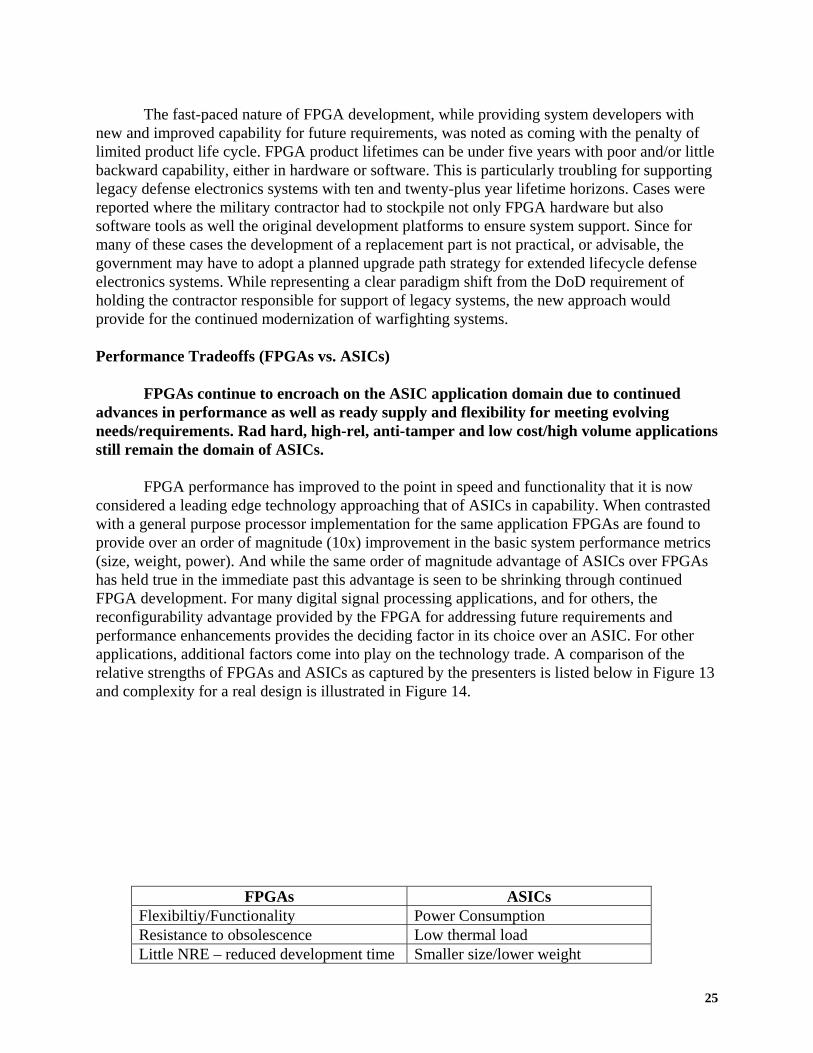
The fast-paced nature of FPGA development, while providing system developers with new and improved capability for future requirements, was noted as coming with the penalty of limited product life cycle. FPGA product lifetimes can be under five years with poor and/or little backward capability, either in hardware or software. This is particularly troubling for supporting legacy defense electronics systems with ten and twenty-plus year lifetime horizons. Cases were reported where the military contractor had to stockpile not only FPGA hardware but also software tools as well the original development platforms to ensure system support. Since for many of these cases the development of a replacement part is not practical, or advisable, the government may have to adopt a planned upgrade path strategy for extended lifecycle defense electronics systems. While representing a clear paradigm shift from the DoD requirement of holding the contractor responsible for support of legacy systems, the new approach would provide for the continued modernization of warfighting systems. Performance Tradeoffs (FPGAs vs. ASICs)
FPGAs continue to encroach on the ASIC application domain due to continued advances in performance as well as ready supply and flexibility for meeting evolving needs/requirements. Rad hard, high-rel, anti-tamper and low cost/high volume applications still remain the domain of ASICs.
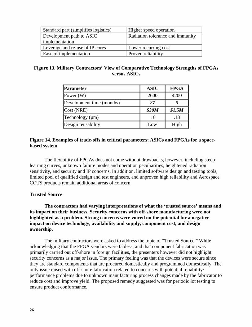
FPGA performance has improved to the point in speed and functionality that it is now considered a leading edge technology approaching that of ASICs in capability. When contrasted with a general purpose processor implementation for the same application FPGAs are found to provide over an order of magnitude (10x) improvement in the basic system performance metrics (size, weight, power). And while the same order of magnitude advantage of ASICs over FPGAs has held true in the immediate past this advantage is seen to be shrinking through continued FPGA development. For many digital signal processing applications, and for others, the reconfigurability advantage provided by the FPGA for addressing future requirements and performance enhancements provides the deciding factor in its choice over an ASIC. For other applications, additional factors come into play on the technology trade. A comparison of the relative strengths of FPGAs and ASICs as captured by the presenters is listed below in Figure 13 and complexity for a real design is illustrated in Figure 14.
FPGAs ASICs Flexibiltiy/Functionality Power Consumption Resistance to obsolescence Low thermal load Little NRE – reduced development time Smaller size/lower weight
26
Standard part (simplifies logistics) Higher speed operation Development path to ASIC implementation
Radiation tolerance and immunity
Leverage and re-use of IP cores Lower recurring cost Ease of implementation Proven reliability
Figure 13. Military Contractors’ View of Comparative Technology Strengths of FPGAs versus ASICs
Parameter ASIC FPGA Power (W) 2600 4200 Development time (months) 27 5 Cost (NRE) $30M $1.5M Technology (µm) .18 .13 Design reusability Low High
Figure 14. Examples of trade-offs in critical parameters; ASICs and FPGAs for a space-based system
The flexibility of FPGAs does not come without drawbacks, however, including steep learning curves, unknown failure modes and operation peculiarities, heightened radiation sensitivity, and security and IP concerns. In addition, limited software design and testing tools, limited pool of qualified design and test engineers, and unproven high reliability and Aerospace COTS products remain additional areas of concern. Trusted Source
The contractors had varying interpretations of what the ‘trusted source’ means and its impact on their business. Security concerns with off-shore manufacturing were not highlighted as a problem. Strong concerns were voiced on the potential for a negative impact on device technology, availability and supply, component cost, and design ownership.
The military contractors were asked to address the topic of “Trusted Source.” While acknowledging that the FPGA vendors were fabless, and that component fabrication was primarily carried out off-shore in foreign facilities, the presenters however did not highlight security concerns as a major issue. The primary feeling was that the devices were secure since they are standard components that are procured domestically and programmed domestically. The only issue raised with off-shore fabrication related to concerns with potential reliability/ performance problems due to unknown manufacturing process changes made by the fabricator to reduce cost and improve yield. The proposed remedy suggested was for periodic lot testing to ensure product conformance.

27
In general the military contractors expressed strong concerns and reservations with the idea of a Trusted Source especially as it impacts supply, technical advancement, cost, design authority, competitiveness and design ownership. The specific areas of radiation hardness, reliability and IP security were singled out with a suggestion made that the government “certify” the designs in these areas. The benefits of establishing a domestic foundry for radiation hardened devices was also offered. Future trends/needs
Standardization at the hardware and design software levels required for portability both within and across vendor’s products is needed. A seamless design interface between CAD tools and VHDL coding would allow designers to tap the full potential of FPGA architectures for sensor nodes, reconfigurable computing and system on a chip-like performance.
FPGA usage is projected to continue to increase in military systems as a result of continued improvements in performance and capability. A vision for the future is reconfigurable high performance FPGAs with embedded computing for sensor/system functions/nodes. Re-programming satellites and weapons systems on the fly for new capability and extended missions is also a goal. These and other applications will be enabled with faster, more efficient FPGAs programming using open architecture block design tools in a seamless design environment. Portability across device families, competitor’s products and different platforms will be the norm due to the acceptance of hardware and software standards. Government weapons programs will plan for regular product upgrades to take advantage of technology improvements. Structured ASICs and rad-hard processors employing advanced materials will compete with FPGAs for specific requirements, including Space. Ultimately the slowing of Moore’s’ Law as the device scale size advances to the deep sub-micron region will require the development of radically new technologies to overcome basic device physical limitations. Space applications will likely be impacted first due to problems with increased radiation sensitivity. Findings The primary findings of the military contractor presentations are: • FPGAs have found widespread use and acceptance in digital military electronics systems.
Domain of applicability is growing at the expense of general purpose processor and ASIC solutions due to functionality, availability and development/prototyping advantages.
• Processing speed, power consumption/dissipation and functionality are the primary performance selection metrics for applications. Low NRE cost, availability, and reduced development time are economic selection drivers.
• Reconfigurability to address evolving requirements and extend mission life remains a selection driver. This is especially important for long life, remote platforms, such as satellites.
• Application for space and harsh military environments is still problematic due to unknown reliability problems and/or lack of design information and qualification/radiation immunity testing.

28
• System design tools lag hardware in capability and ease of use serving to limit the realization of FPGA technology for military applications.
• Engineering CADRE skilled in the design and application of FPGAs in military electronics system design is scarce.
• There is no standardization among FPGA hardware and design software. This restricts portability of designs among and across vendor’s product lines.
• Short FPGA product life cycle is at odds with military legacy system logistic demands. New paradigm required in the government for planned upgrades.
• Trusted Source concept viewed as potentially restricting competition, reducing technology advances, increasing cost and reducing supply.
• Security concerns with FPGAs not viewed as a severe problem due to domestic procurement of standard and programming control. Battery back-up and encryption storage methods are viewed as solutions to be implemented as required.
• Off-shore fabrication not identified as a major concern except for the lack of visibility into processing changes at the manufacturer and their potential detrimental affect on performance/reliability. Periodic lot testing suggested as solution.

29
Synopsis of Rad-Hard Presentations Radiation Effects on Programmable Devices Programmable devices can be degraded, destroyed or interrupted by the various radiation effects in the natural and nuclear radiation environment. These effects include total dose from natural and nuclear enhanced charged particles, dose rate upset and latchup from nuclear transient effects and a number of single-event effects from cosmic rays, protons and neutrons.
For programmable devices, total dose effects include increased operating and leakage currents and reductions in circuit performance. For example, FPGAs that include a charge pump circuit can be very susceptible to increased start-up currents. In addition, EEPROM-based FPGAs are very sensitive to charge loss on their floating-gate or charge storage layers. However, some advanced programmable FPGAs can be relatively robust to isolation-type leakage and have failure thresholds about 100 - 200krad. In these complex devices, it is important that the total dose sensitivity is tested on real circuits and under worst-case bias conditions. Improved processes and some hardening by design methods are effective to harden against total dose effects. Hardening to total dose effects is not particularly challenging for FPGAs (flash-based FPGAs are a particular exception).
For critical military systems, dose-rate effects must be considered. In particular, dose- rate-induced burnout and latchup cannot be tolerated. Programmable FPGAs fabricated on bulk silicon substrates are typically susceptible to dose-rate induced latchup (e.g., Atmel). By implementing epitaxial substrates, the sensitivity to latchup in CMOS/bulk technology can usually be avoided (e.g., Xilinx Vertex). Silicon-on-insulator (SOI) technology is also effective in reducing dose rate effects. Assuring dose rate survivability is generally not a problem in contemporary circuits. Programmable devices are particularly sensitive to single event effects (SEE) including single event upsets, single event transients, and single event dielectric rupture. In particular, single event upsets in the configuration memory of programmable FPGAs lead to single-event functional interrupts (SEFIs) that result in the complete loss of control over the device operation. SEFIs are particularly troublesome to accurately analyze or to mitigate (harden against). SEFI-induced configuration changes may not be possible to reset or reprogram while in orbit. For this reason, if an FPGA is to be useful in space its configuration memory must be radiation hard. In addition to data memory upsets, other examples of single event upsets that disrupt functionality include clock-line upsets, data-path interruption faults, bus-driver contention faults, etc. SEE effects are most effectively handled by design methods that either harden memory cells, latches and logic devices or using on-chip error correction. Global SEE error-mitigation methods are also used but usually require extensive overhead and may not be completely effective.
In addition to nondestructive single events, some FPGAs are sensitive to destructive single events such as latchup. Latchup can lead to destructive circuit burnout. Gate oxide or other dielectric (antifuse) rupture can lead to the single-event to upsets in the configuration in OTP (one time programmable) devices.

30
Radiation Effects and Reliability Evaluation Methods
Recently, low-level failures were observed in some Antifuse-type FPGAs. As these FPGAs are used in several space systems, an extensive investigation (including the FPGA vendor, system developers and government labs) was undertaken to address this reliability issue. Failures were traced to both device design and process-induced anomalies that were not discovered during routine reliability qualification. As a corrective measure the antifuse has been redesigned and processing implemented at a different fabrication facility. This experience implies the need for additional reliability qualification for advanced FPGAs to augment vendor testing because the FPGA vendor has limited insight into the process at the foundry or the FPGA process is not mainstream. This additional reliability investigation is particularly important when hardening-by-design methods are employed. Reliability will be a major driver for applying FPGAs in missiles and space.
The long duration of military as well as some commercial/civil space missions require
that payloads be designed for reliable autonomous operation thus minimizing or eliminating ground intervention. Therefore, very accurate error prediction and validation methods are required to estimate the wide range of SEE effects due to space radiation and the need for error correcting methods. Commercial industry and some universities are addressing the error estimation problem for circuits operating in the terrestrial environment and developing analysis tools. However, these tools are not able to estimate the low cross section errors and must be updated to be useful for error analyses in the space environment. The radiation error analysis problem in advanced FPGAs is also difficult because the analyst usually does not have access to all FPGA circuit details and/or limited access to vendor provided intellectual property. Planned FPGA Radiation Hardening Projects
In recent surveys sponsored by the Radiation Hard Oversight Council (RHOC), space system developers were requested to provide their microelectronics needs for future systems. The surveys showed a need for advanced radiation hard FPGAs with densities in the 4-16-million gates (see Figure 15).
FPGA Requirement
2003-2007 2008-2012
Usable Gates > 1M > 10M Operating Power (uW/Gate/MHz)
<[email protected] <[email protected]
Operating Voltage (V) 2.5-1.8V 1.5-1.0V Radiation Hardness (TD, DR, SEE)
High High
Figure 15. RHOC survey of determined needs for advanced rad hard FPGA requirements.
In order to meet these DoD missile- and space-system needs (accelerating as the
commercial technologies scale) for radiation hard programmable devices, a series of FPGA hardening projects have been defined in the RHOC roadmap (see Figure 16) for radiation hard microcircuit development.

31
Figure 16. FPGA technology capabilities planned from the RHOC roadmap (May 04).
These S&T and productization/qualification (P&Q) projects are coordinated among many
government organizations including DTRA, AFRL, AF SMDC, USN SP, MDA, DOE (Sandia) and NASA. These projects include: • The development of a fully radiation-hard, 250k – 1M gate antifuse-type FPGA using the
150nm CMOS/bulk technology. This program is under way and will demonstrate the first rad hard FPGA product by early 2006. In addition, P&Q efforts are planned.
• The development of a virtually-hard FPGA using a radiation hard ASIC to effectively harden the configuration memory of commercial SRAM-based FPGAs. This ongoing effort will provide a radiation tolerant programmable FPGA that is not subject to SEE effects. This effort includes a P&Q test development effort with application to missile defense.
• Development of a radiation hardened, advanced (>3 million gates) reprogrammable FPGA based on non-volatile technology using commercial 90nm-CMOS technology. Hardening by design is proposed with a planned start in late FY05.
• Develop a radiation hard reconfigurable, 3 million gate, SRAM-based FPGA using 90nm CMOS technology.
Additional Technology Development Needs The following development needs must be addressed in order to apply advanced FPGA technologies (those using technologies at 90nm and beyond) in missile and space systems: • Analysis, modeling and test methods need to be developed that can validate the FPGA
configuration sensitivities for the space and nuclear radiation environment and not just the terrestrial environment. The models and test methods must be cost effective and comprehensive with close to 100 percent fault coverage.
• Reliability and aging analysis (understand mechanisms) and acceleration test methods must be developed for these advanced FPGA devices to validate the long-term operation of the circuits in space. These evaluation procedures are needed particularly for hardened by design approaches because there is limited process qualification for these commercial technologies.

32
• Develop robust (inherently radiation hard and reliable) non-volatile technologies (such as metal-ferroelectrics-insulator, gate-controlled cell with non-destructive readout, energy programmable resistance change or a high-density MRAM technology). Candidate technologies must be easily insertable into or are compatible with a radiation hard CMOS fabrication flow to support radiation hard reprogrammable devices that are key to the development of radiation-hard systems-on-a-chip. These technologies can be designed with higher density and significantly lower power than volatile-SRAM-type FPGAs.
Findings from the Rad Hard Sessions • Continue the development of radiation hard FPGA devices that include OTP devices and
programmable devices that are immune to configuration upsets (SEFI). Invest in hardening methods that include both design and process modification to extend to FPGAs using sub-100nm technology.
• Research in analysis and modeling efforts that can validate sub-100nm FPGA circuits for SEU sensitivities in a cost-effective and comprehensive way. This research should include new innovative test methods.
• Develop a mechanism-based aging and reliability model that can be used to effectively accelerate failure modes in advanced technologies used in programmable devices.
• Continue to investigate robust non-volatile technologies that are compatible with or can easily be implemented in a radiation hard CMOS flow serving as the basis for a radiation hard reprogrammable system-on-a-chip technology.

33
Future Vision for FPGA Technologies
Programmable logic devices have grown from a few hundred gates to near ten million gates in the last two decades. In comparison with ASICs that require substantial non-recurring engineering cost in the design and fabrication, FPGAs can be configured into system on a chip by the development of programs on commodity chips at much lower cost. With the increase in electronic content in weapon systems but at the same time facing budget pressure, DoD is deploying more FPGAs rather than ASICs, due to lower cost, flexibility, and reprogrammability. As the density of FPGAs continues to increase, FPGAs increasingly will be used to meet the high performance demands of military systems. However, standard cells in commercial FPGAs and development tools are adequate for civilian applications but not sufficient for military unique applications. One of the most critical problem for military application of FPGAs is to insure the security of their contents. Thus future military designs must provide intrusion protection and deny reverse engineering. Technology Evolution Over the past several decades, microelectronics has been following Moore’s Law. Subsequently the Law has been expanded to apply to such things as gate length, metal pitch, clock speed, and price per bit. Needless to say, Moore’s Law is a consequence of microelectronics technology and its economics, and does not derive from the laws of physics. Although much of the COTS VLSI chips can be used in military systems, often there are unique DoD requirements that COTS chips cannot meet. Some of these DoD requirements include expanded operating range of temperatures, higher reliability and dependability in harsh environments (shock, humidity, high temperature, and radiation). An additional unique DoD requirement is the need for device and data security in the battlefield. For some systems operating in space and/or nuclear environment, radiation hardened electronics is necessary, which is not a concern for commercial electronics. There are unique requirements for classified applications (e.g. fusing) including MEMS technology. For these reasons, DoD invests substantial amount in the research and development of microelectronics to meet its needs. The commercial semiconductor electronics industry is guided by the ITRS (International Technology Roadmap for Semiconductors) Roadmap and the evolution of ASICs and FPGAs is anticipated to track with this roadmap. The dominant semiconductor in industry worldwide today is bulk silicon technology, with its long history of development and fabrication. The Roadmap is an industrial assessment of the current state of fabrication technology and a projection into the near and far future. Figure 17 shows the near-term and long-term projection of the technology nodes.

34
0
20
40
60
80
100
120
2003
2005
2007
2009
2011
2013
2015
2017
DRAM 1/2 pitch (nm)
MPU physical gatelength (nm)
Figure 17. Near-term and long-term projection of technology nodes
Note: For years 2011, 2014, and 2017, the Roadmap does not make a projection. The data points for these years are interpolations of the adjacent years. The 2003 version of the Roadmap showed that in the year 2004 the dominant technology is at 90 nanometer (nm, or 10-9 meter) for the DRAM ½ pitch, and the physical gate length for MPU (Micro-Processor Unit) is 37nm. By 2010, the DRAM ½ pitch will shrink to 45nm, and the MPU physical gate length will be down to 18nm. By the year 2015, the MPU physical gate length will be down to 10nm. Silicon CMOS (complementary metal oxide semiconductor) devices at that dimension have already been demonstrated by Intel. Another way to look at the Roadmap is to look at the projection on the number of transistors on the chip. The following chart shows the projected number of transistors in millions (again, for the years 2011, 2014, and 2017 the numbers are interpolated). As can be seen in Figure 18, the number of transistors on a chip is projected to increase exponentially. By the year 2015 it is projected that 6 billion transistors will be integrated on a chip. But the rate of increase is anticipated to slow down considerably beyond 2015 due to heat dissipation and other factors.
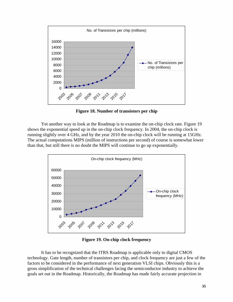
35
No. of Transistors per chip (millions)
02000400060008000
10000120001400016000
2003
2005
2007
2009
2011
2013
2015
2017
No. of Transistors perchip (millions)
Figure 18. Number of transistors per chip
Yet another way to look at the Roadmap is to examine the on-chip clock rate. Figure 19 shows the exponential speed up in the on-chip clock frequency. In 2004, the on-chip clock is running slightly over 4 GHz, and by the year 2010 the on-chip clock will be running at 15GHz. The actual computations MIPS (million of instructions per second) of course is somewhat lower than that, but still there is no doubt the MIPS will continue to go up exponentially.
On-chip clock frequency (MHz)
0
10000
20000
30000
40000
50000
60000
2003
2005
2007
2009
2011
2013
2015
2017
On-chip clockfrequency (MHz)
Figure 19. On-chip clock frequency
It has to be recognized that the ITRS Roadmap is applicable only to digital CMOS
technology. Gate length, number of transistors per chip, and clock frequency are just a few of the factors to be considered in the performance of next generation VLSI chips. Obviously this is a gross simplification of the technical challenges facing the semiconductor industry to achieve the goals set out in the Roadmap. Historically, the Roadmap has made fairly accurate projection in
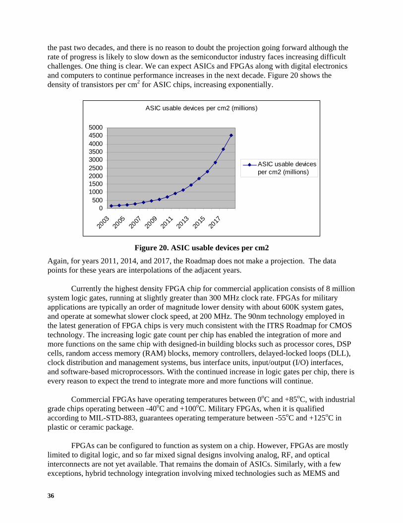
36
the past two decades, and there is no reason to doubt the projection going forward although the rate of progress is likely to slow down as the semiconductor industry faces increasing difficult challenges. One thing is clear. We can expect ASICs and FPGAs along with digital electronics and computers to continue performance increases in the next decade. Figure 20 shows the density of transistors per cm2 for ASIC chips, increasing exponentially.
ASIC usable devices per cm2 (millions)
0500
100015002000250030003500400045005000
2003
2005
2007
2009
2011
2013
2015
2017
ASIC usable devicesper cm2 (millions)
Figure 20. ASIC usable devices per cm2
Again, for years 2011, 2014, and 2017, the Roadmap does not make a projection. The data points for these years are interpolations of the adjacent years. Currently the highest density FPGA chip for commercial application consists of 8 million system logic gates, running at slightly greater than 300 MHz clock rate. FPGAs for military applications are typically an order of magnitude lower density with about 600K system gates, and operate at somewhat slower clock speed, at 200 MHz. The 90nm technology employed in the latest generation of FPGA chips is very much consistent with the ITRS Roadmap for CMOS technology. The increasing logic gate count per chip has enabled the integration of more and more functions on the same chip with designed-in building blocks such as processor cores, DSP cells, random access memory (RAM) blocks, memory controllers, delayed-locked loops (DLL), clock distribution and management systems, bus interface units, input/output (I/O) interfaces, and software-based microprocessors. With the continued increase in logic gates per chip, there is every reason to expect the trend to integrate more and more functions will continue. Commercial FPGAs have operating temperatures between 0oC and +85oC, with industrial grade chips operating between -40oC and +100oC. Military FPGAs, when it is qualified according to MIL-STD-883, guarantees operating temperature between -55oC and +125oC in plastic or ceramic package. FPGAs can be configured to function as system on a chip. However, FPGAs are mostly limited to digital logic, and so far mixed signal designs involving analog, RF, and optical interconnects are not yet available. That remains the domain of ASICs. Similarly, with a few exceptions, hybrid technology integration involving mixed technologies such as MEMS and

37
optics is not implemented in FPGAs. Again the non-recurring engineering (NRE) cost of design mask making, and manufacturing for ASIC chips can be quite high, whereas the hardware cost of FPGA is low. However, for applications where millions of chips are produced, the NRE cost of ASICs may be justified. Performance of custom designed ASIC chips is usually higher than systems implemented on FPGAs. These are tradeoffs system designers must make, based on economics and technical requirements. Still, there is no doubt that in many applications FPGAs can replace ASICs at a much lower developmental cost. Beyond Silicon The continued scaling of silicon CMOS technology, in accordance with the ITRS Roadmap, likely will end by the year 2020 with the 16nm node (7 nm physical channel length). With the end of the Roadmap in sight, industry observers are increasingly concerned that alternative technology must be found, knowing the long lead-time it is necessary to develop the manufacturing infrastructure. University researchers are increasingly turning to basic research on emerging materials and devices. The first application for new devices to replace silicon CMOS may be in the area of memories such as DRAMs. Once it is proven to be reliable and manufacturable in memories, the devices will be applied to logic circuits. Given that silicon CMOS scale still has about two more decades to go, it is safe to say that any CMOS replacement technology is at least that far away. Even for memories, the lead time for introduction of new process technologies is at least 15 years. For random logic and ASIC type of applications and including FPGAs, the timeline is at least two or three decades away. Furthermore, advances on 3-D integrations and multi-chip technology will carry the CMOS FPGA technology well beyond our lifetime. Three dimensional integration technologies will likely become more common and accepted over the next decade. They will find particular application first in truly wire-limited circuits, FPGAs being the prime example. 3D technologies will enable the FPGA to be broken into constituent circuit partitions, such as a layer of memory and a layer of configurable logic elements. In this scenario, SRAM or flash memory could be employed as the configuration memory. 3D potentially solves the wiring challenge of 2D planar integration and offers high bandwidth connections among the various layers of a 3D IC. Field programmable analog circuits are also an interesting emerging area. Previous attempts at this were largely unsuccessful due to poor semiconductor efficiency and large parasitics due to the interconnect matrix. Scaled silicon device technology has boosted analog performance and increased semiconductor efficiencies to the point that field programmable analog is worth reconsidering. In general, a field programmable analog circuit is likely to have relatively few connections. Both laser created links and antifuse techniques may provide reasonable performance, although the true metal-metal contact of the laser link or via array will most likely provide the best overall linearity and best RF properties. Laser links are interesting as they offer a method of customizing a circuit post-fabrication, but still provide a metal-metal interconnect and via. Opportunities and Challenges
38
While the electronic content of deployed systems is increasing, DoD is faced with a shrinking budget and diminishing manufacturing supply of traditional military microelectronic parts. Although military market demands the highest performance, new designs for military applications exploiting the latest technologies traditionally have lagged the civilian counterpart. On the other hand, improvements in design and reliability have allowed plastic packages to replace the traditional ceramic packages for military parts. Since 1994, DoD has allowed the defense contractors to use commercial parts but the end system must meet the overall performance requirements. This opened the door and greatly accelerated the use of FPGAs in plastic packages whenever appropriate. On the other hand, some applications with extreme temperature variations, long storage life, high humidity, and radiation hardening will continue to have to meet MIL-STD-883 requirements. Before making some observations, it is necessary to make some assumptions. First it is assumed that the technology for FPGAs will advance along with semiconductor industry. In other words, next generation FPGAs will have solved the problems with reliability, power dissipation, interconnect routing, etc. Particularly it is assumed that the military and aerospace FPGAs will be meeting the military standard requirements for operating temperatures, radiation hardening, electro static discharge protection, and humidity resistance. As the technology evolves, it is possible that FPGAs may follow other high performance microchip technology such as flip-chip bonding, multi-chip modules (MCM), and 3-D integration. Gradually FPGAs may also incorporate mixed signal designs and hybrid technologies. Only planar, commodity single-chip types of FPGAs are considered in this analysis. Based on these assumptions, the question is raised, what role FPGAs will play in the defense electronics enterprise? Analysis of the trends has led to the following observations, opportunities, and challenges for the military. FPGA vs ASIC With the rapid advances in system gate density, FPGAs can be configured as SoC for many military applications such as digital signal processing. For many digital system applications, the performance of FPGAs can meet requirements. It is entirely possible that for the military, FPGAs will replace ASICs for the reasons mentioned previously, except for cases where extremely high performance, hybrid technology integration (e.g. fusing incorporating MEMS device on the chip), mixed signals (e.g. analog, digital, and RF), and unique designs are required. The use of ASIC design is justified only when the performance cannot be met otherwise. But with the technology advances, there are not many digital system requirements that cannot be met with FPGAs. Cost One of the reasons FPGAs are increasingly replacing ASICs is the much lower cost. Non-recurring engineering cost of custom designed ASICs, including design, simulation, mask sets, and fabrication is very high as compared to algorithms that can be implemented on off-the-shelf FPGAs. The high cost of NRE of ASIC is justified only when there is large-volume production of the chips to mitigate the high upfront cost. However, military parts are typically low-volume productions, resulting in extremely high cost per part. In the past, military parts required high performance and cost was a secondary consideration. But today, with shrinking defense budget,

39
affordability is an important consideration for defense technology, and FPGAs can significantly lower the cost of electronic content in systems. Building Blocks Many FPGAs in addition to the conventional configurable logic blocks (CLB) have added custom designed cells. However, these standard cells are used mostly as core computing engines in conventional computing and signal processing. Standard cells are fine for civilian applications but are not sufficient for unique defense applications. There may be unique military requirements that cannot be programmed with standard cells, such as high-speed electronic warfare signal identification and sorting and new algorithms for encryption and decryption. Therefore, it may be necessary to develop a set of standard cells that are unique to military applications, in order to facilitate the use of FPGAs in military systems. Design Tools Current generations of design and development tools are adequate for civilian applications and most digital military applications. However, defense design has unique requirements that are not imposed on commercial products, such as the need for self-test to insure correct operation in the weapon system. Furthermore, as the gate density of FPGAs continues to increase, greater demands are placed on the design tools to exploit all the available logic gates and to efficient routing on the chip. Also as the number of gates reach into the millions, multi-level simulation of the entire chip becomes necessary to do timing checks. Because COTS FPGAs parts are increasingly used in military systems, it is necessary to develop design and development tools for military applications. Increasingly DoD and its contractors are becoming system designers and integrators rather than custom designer of ASIC parts. Therefore it is important to make design tools available for unique military implementations on FPGAs. Security Reverse engineering (RE) of computational programs and algorithms implemented on FPGAs, as well as the protection of IP, is a concerned in commercial applications, and is a serious problem for the military. Various techniques and technologies have been developed to prevent RE and to protect IP to insure security have been developed for FPGAs, and are adequate for the commercial marketplace. For the military, security of the contents of the chips is a critical problem that is not adequately addressed by the civilian counterpart. If the chips are lost in the battlefield, it is crucial to prevent the compromise of the content of the chips. Some technologies, such as Quicklogic’s metal-to-metal ViaLink technology, is more secured against RE. Furthermore, the technology is non-volatile, and does not involve the downloading of programs to the SRAM on start up. For the wider application of FPGAs to the military, more secured technology to prevent RE, including encryption of data and the possibility of self-destruct mechanisms, need to be developed. Summary of Future Vision The inexhaustible march of semiconductor technology will continue for the foreseeable future in accordance with Moore’s Law. Along with the DRAM, MPU, and other

40
microelectronic chips, density of system gates will continue to increase with CMOS technology. Even though there is substantial research with futuristic devices to replace silicon CMOS, it is very unlikely to see FPGAs implemented with these emerging devices for many decades to come. Furthermore, advances in multi-chip technology such as flip-chip bonding and 3-D integration, will extend the performance of FPGAs well beyond the current and next generation of FPGAs. Performance of FPGAs today is becoming comparable to ASIC chips a decade ago. With abundant configurable logic gates, SoC implemented on FPGAs and without resorting to ASICs is increasingly becoming a reality. The electronic content of weapon systems continues to increase. Due to the flexibility and much lower cost, FPGAs are increasingly being utilized in systems, displacing ASIC parts. As the gate density of FPGAs, as well as the clock speed, continues to increase to allow SoC implementation, FPGAs can meet the performance requirements of many military systems. High density FPGAs contain standard computational cells and building blocks that are needed in conventional civilian applications. Military application may require unique designs and functions that cannot be met by the conventional computing cores. To insure that FPGAs will be available to meet defense needs, it is necessary to develop a set of military standard cells and computing engines that would be implemented in an FPGA. Military designs have unique requirements that go beyond their civilian counterparts. Current generation of design and development tools for FPGAs have limitations in terms of addressing military designs such as the need to implement on-line self-tests. As defense electronic contractors become more and more as system integrators rather than ASIC designers, it is important to make available FPGA development tools that are needed for military designs. Security remains a serious issue for application of FPGAs in military systems. If the chip is captured by the adversary, the program and algorithm can be reversed engineered to develop countermeasures against the weapon. Various techniques and technologies have been developed for FPGAs to make it difficult to reverse engineer the programs. But still for wider military applications to mission critical systems, a greater degree of security must be investigated and developed for FPGAs. In spite of that, cost consideration will push for greater and greater deployment of FPGAs in military systems.

41
Observations, Findings and Recommendations
The FPGA STAR workshop included Government Caucus sessions and was followed by a Government working group session that identified and refined general observations about the field, key findings of the FPGA study and recommendations for the DoD. This section collects these general observations, findings and recommendations. General Observations These are general observations about the FPGA field and their use by DoD and its contractors. • Rapid FPGA market segment growth (>15%/year for most vendors) & FPGA flexibility and
power continue to escalate; • Migration of commercial and Government applications to use FPGAs due to cost, time-to-
completion, flexibility (in spite of performance penalties) and potential IP and security risks; • Manufacture and assembly of high performance FPGAs mostly performed offshore; • Government applications account for <10% of overall FPGA market; • Leading edge vendors are incorporating more hard cores & functionality per die; • Vendors focused on near term solutions (3-5 yrs); • No real security analysis/implementation exists in FPGAs (not a commercial priority due to
short product cycles, although some offer limited security features (encryption, one time programmability, etc.);
• Radiation hardening is an issue – no commercial driver & market for this – vendors not focusing leading edge efforts on this area;
• FPGA technology is immature and changing fast – lack of standards, benchmarking, interoperability, common software design tools, etc.;
• FPGAs offer in-field software upgrades – potential solution for lifecycle issues
Key Findings Here are the key findings that were established from the FPGA STAR. • Common Government requirements and concerns include:
• Power, size, density, cost, long life cycle, reliability, trusted sources, packaging, memory on board, on-chip processors, hybrid analog and digital, partial reconfiguration, good software design tools, single event effects
• Reliability of FPGAs is poorly understood leading to unexpected system vulnerabilities and failures: • Immature FPGA technology has already been incorporated in military systems; • Vendor deployment sometimes premature; • Low firmware density (i.e., lower interconnect utilized) has greater performance/lower
risk • Vendor specific software design platforms are immature:
• not well integrated, and not interoperable among different vendors – “Expert user” friendly
• Lack of common definitions, standards and benchmarking for performance and capacity hinder technology tradeoffs

42
• Design, validation, testing, verification and feedback is lacking from primary vendors –available from 3rd party vendors
• Security: No security analysis – security is somewhere between nonexistent and poor • Security means many different things to the vendors: configuration not lost on power off,
config needs to be encrypted, config needs to be stored on chip so that it is never seen, config needs to be blocked to stay on chip, trusted sources for IP cores – no back doors
• A number of advanced nonvolatile-memory FPGA approaches are being evaluated • Technology challenges for a low-leakage, 6-transistor SRAM cell beyond 65nm node – not
clear if this technology will scale • Architectural and circuit innovations are needed to improve leakage currents and other
physics limitations • Fabless FPGA vendors have limited control and auditing capability over the manufacturing
and process control creating reliability & security vulnerabilities • FPGA hardware and software requires the whole software quality management cycle
• Quality of HW and SW products espoused by the vendors was not confirmed by the users • Floating-point arithmetic not generally available on FPGAs as a hard core • Mixed signal cores are lacking • Advanced designs for radiation hardened FPGAs need DoD stimulation Recommendations
The FPGA STAR Committee has refined the observations and findings into a set of recommendations that we suggest to the DoD.
• Initiate a benchmark activity to identify and compare performance and capacity of
FPGAs by a vendor neutral entity. This is a perspective widely acknowledged by vendors, users, and academia – there is no consistent approach for the comparison of different FPGA technologies. This activity will likely require the development of a set of metrics.
• Perform a comprehensive risk and security assessment of using FPGAs in category 1 electronics. It is unknown how secure the uses of FPGAs are and yet they are being deployed throughout the DoD and IC communities – even in category 1 applications. This issue needs a careful evaluation and assessment.
• Address S&T gaps a. Develop software for advanced design, automation, and verification capabilities. This
effort focuses on the issue that current tools are not seamlessly integrated - leading to a high degree of inefficiency. The DoD interest in assuring that such tools are developed stems from the need for new capabilities based upon FPGAs and their rapid insertion into military systems.

43
b. Support research into materials and process roadblocks beyond 65 nm node (e.g. 6-T transistor cell). Inherent limitations in the device physics of the 6-T SRAM cell, such as increased leakage currents, as it is scaled beyond the 65nm node may lead to the inability of the FPGAs to follow Moore’s Law over the next five to seven years achieving higher density, higher speed, at manageable dissipation levels. DoD has an interest in surmounting barriers to higher levels of integration since such capabilities will lead to increased functionality of their electronic systems.
c. Support research into physics of failure for FPGAs. Develop mechanism-based aging and reliability models that can be used to effectively accelerate failure modes in advanced technologies used in FPGAs. The DoD requires highly reliable components in its electronics systems. The need to develop mechanism-based aging and reliability models that can be used to effectively accelerate failure modes in advanced technologies used in FPGAs is a DoD priority.
d. Stimulate architecture and circuit innovation including nonvolatile memory, mixed signal and floating point hard cores.
e. Develop radiation hard capability for advanced FPGAs to include analysis and modeling efforts that can validate sub-100 nm FPGAs for SEU sensitivities. Radiation tolerance in ambient space environments and radiation hardness in strategic nuclear environments are crucial to DoD electronics systems and will not be pursued by the commercial sector.
The DoD needs to understand these Science and Technology areas to be able to better
utilize this technology in their critical electronic systems. A pictorial representation of the interaction between these S&T elements is presented in Figure 21.
Figure 21. Interdependency of S&T Areas on FPGA Applications

44
• Assess design, functionality and complexity vulnerabilities of the fabless foundry model We need to understand the vulnerabilities with significant offshore manufacturing of FPGAs as well as the general lack of detailed control inherent in this business model which is the model of choice for the FPGA vendors. • Determine ability to access a Trusted Foundry for FPGA Manufacturers We need to assess whether it is feasible for FPGA manufacturers to utilize DoD trusted
foundries for the production of FPGA parts (and potentially software) for the DoD applications. • Provide DoD access to the most advanced FPGA technology including radiation hard
and other DoD specific requirements Continue to develop radiation hard advanced (sub-100nm) CMOS technology. Develop FPGA devices that are immune to configuration single-event upsets using both design and process modifications.
• Develop military unique IP cores for Advanced FPGAs Standard IP cores are not sufficient for all military applications, for example mixed signal
cores might be desirable for some applications.

45
Further DoD Implications of the S&T Recommendations DoD Implications of the S&T Gaps • DoD can help guide industry to develop capabilities to more efficiently perform place and
route functions and more efficiently utilize FPGA capacity and functionality through DoD requirements and research programs. This is important because military applications often attempt to fully utilize the capacity of the FPGAs.
• Supporting research into materials and process roadblocks beyond 65 nm node will enable an understanding of the capabilities of the next generation of electronic technologies as well as their limitations and vulnerabilities. This understanding is critical for mission critical applications of this technology. These capabilities are important for the DoD to be able to deploy the most advanced combat and communications systems possible.
• Understanding the physics of failure of FPGAs will enable them to be used with confidence that we know when and why these devices will work as prescribed in the harsh environments in which the DoD may field these devices. This area of concern goes significantly beyond the level of commercial interest in these topics.
• Supporting university, industry and government-based research into architectures and circuit innovations for high performance will complement progress that the FPGA vendors are doing for commercial applications (generally lower performance).
• Radiation hard FPGAs are significantly less capable than their commercial counterparts – yet these parts are being deployed into critical DoD missions – the need exists to facilitate the generation of higher performance rad-hard FPGA technologies for which there is little or no commercial driver. A critical part of this is the understanding through simulation and analysis that accurately represent device behaviors at small feature sizes.

46
Summary and Conclusions FPGAs are rapidly becoming an essential flexible integrated circuit building block of choice for commercial and defense systems. While having higher power consumption than custom ASICs of comparable capability, their low cost, lack of hardware chip development NRE, and flexibility, leads to very cost effective, rapid prototyping and product development. As their performance, complexity, cost and capacity have improved, these devices have begun to challenge the use of ASICs throughout military electronic systems. The STAR examined two crucial elements of FPGA technology: 1) component and subsystem technologies and 2) FPGA microsystem application design tools and methodologies. The status of the FPGA technologies was assessed in terms of capabilities, cost, risk, implementation (including design) security, performance vis-à-vis alternative technologies such as ASICs. The STAR confirmed that FPGAs are a crucial electronic component in many DoD systems and will likely continue to be so. However the STAR also uncovered several areas of concern that AGED believes should be addressed by the DoD. Many of these concerns are due to the inherent differences between the rapidly expanding commercial markets for FPGAs and the military market which is geared to performance assurance and long product life cycles. An overwhelming majority of the FPGA business is commercial in nature limiting the leverage of the DoD. The STAR covered all major aspects of the FPGAs for military use and identified key areas of concern. The traditional role that FPGAs have played as “glue chips” in electronic systems has changed as their complexity and functionality has dramatically increased and is expected to continue to continue. Military users of FPGAs have replaced ASICs drastically reducing time-to-product and have done so in spite of the performance penalties. The STAR has produced a set of General Observations, Key Findings and Recommendations. In particular, the STAR has produced actionable Recommendations about comparisons of FPGAs, security considerations in using FPGAs, significant science and technology gaps, assessing vulnerabilities of the manufacturing model for FPGAs and addressing DoD specific requirements for FPGAs.
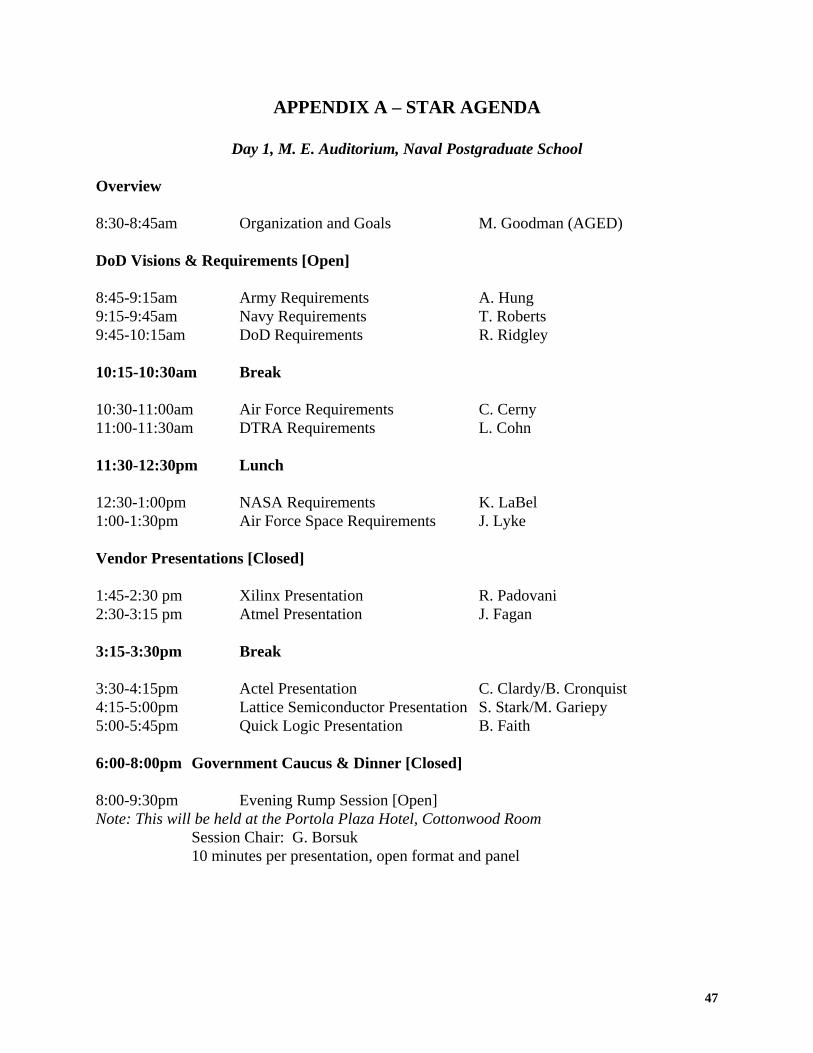
47
APPENDIX A – STAR AGENDA
Day 1, M. E. Auditorium, Naval Postgraduate School
Overview 8:30-8:45am Organization and Goals M. Goodman (AGED) DoD Visions & Requirements [Open] 8:45-9:15am Army Requirements A. Hung 9:15-9:45am Navy Requirements T. Roberts 9:45-10:15am DoD Requirements R. Ridgley 10:15-10:30am Break 10:30-11:00am Air Force Requirements C. Cerny 11:00-11:30am DTRA Requirements L. Cohn 11:30-12:30pm Lunch 12:30-1:00pm NASA Requirements K. LaBel 1:00-1:30pm Air Force Space Requirements J. Lyke Vendor Presentations [Closed]
1:45-2:30 pm Xilinx Presentation R. Padovani 2:30-3:15 pm Atmel Presentation J. Fagan 3:15-3:30pm Break 3:30-4:15pm Actel Presentation C. Clardy/B. Cronquist 4:15-5:00pm Lattice Semiconductor Presentation S. Stark/M. Gariepy 5:00-5:45pm Quick Logic Presentation B. Faith 6:00-8:00pm Government Caucus & Dinner [Closed] 8:00-9:30pm Evening Rump Session [Open] Note: This will be held at the Portola Plaza Hotel, Cottonwood Room Session Chair: G. Borsuk 10 minutes per presentation, open format and panel

48
Day 2, M. E. Auditorium, Naval Postgraduate School
Wednesday, 4 August 2004
Academic Presentations [Open] 8:30-8:50am University of Delaware F. Kiamilev 8:50-9:10am Purdue University K. Roy 9:10-9:30am Mayo Clinic E. Daniel Government Vision [Open] 9:30-10:00am DARPA/MTO Vision D. Radack 10:00-10:15am Break FPGA OEMs [Closed] 10:15-11:00am Altera Presentation A. El-Ashmawi/D. Mansur 11:00-11:30am Mercury Computer Presentation J. Bloomfield 11:30-12:00pm Annapolis Micro Presentation P. Stover 12:00-1:00pm Lunch FPGA Application Software Design Tools [Closed] 1:00-1:30pm Mentor Graphics Presentation D. Gardner Military Contractors [Closed] 1:30-2:00pm Honeywell Presentation R. Elmhurst/J. Ramos 2:00-2:30pm Northrop Grumman Presentation R. Calatayud 2:30-3:00pm L-3 Communications Presentation R. Sylvester 3:00-3:15pm Break 3:15-3:45pm Raytheon Presentation R. Branstetter 3:45-4:15pm BAE Presentation H. Livingston 4:15-4:45pm Lockheed Martin Presentation M. Enoch 4:45-5:15pm Boeing Presentation K. Jobe Adjourn 5:15-6:15pm Government Caucus [Closed]

49
APPENDIX B – TERMS OF REFERENCE
DEPARTMENT OF DEFENSE ADVISORY GROUP ON ELECTRON DEVICES (AGED)
SPECIAL TECHNOLOGY AREA REVIEW
ON Field Programmable Gate Arrays (FPGAs)
TERMS OF REFERENCE
PRIMARY OBJECTIVE: The objective of this Special Technology Area Review (STAR) is to provide information that will assist the Department of Defense (DoD) in defining and pursuing a defense-wide application strategy for the use of FPGAs in present and future military information, computer, and sensor systems. FPGAs are rapidly becoming the essential, high performance integrated circuit building block of choice for many commercial and defense systems. As their performance, complexity, cost, and capacity have improved, these devices have begun to challenge the use of ASICs (Application Specific Integrated Circuits) in many electronic systems. In some applications their ability to incorporate built-in core functionality such as those of microprocessors or DSPs have lead to preferred system level solutions over traditional design approaches. Military systems, however, differ from their commercial counterparts in terms of their production volume, radiation tolerance, assured secure functionality, and system lifetimes. The STAR will examine two crucial elements of FPGA technology: 1) component technologies and 2) FPGA microsystem application design tools and methodologies. The status of FPGA technologies will be assessed in terms of capabilities, cost, risk, implementation (including design), security, and performance vis-à-vis alternative technologies such as application specific integrated circuits (ASICs). OBJECTIVES: The STAR’s objectives for components will be to: 1) Determine the state of the art (SOTA) and progress made over the last 5 years, 2) Identify the technical barriers to DoD insertion,

50
3) Identify and prioritize the current FPGA technology with regard to performance, availability, and affordability,
4) Assess likely systems risks/vulnerabilities caused by using this technology, 5) Assess the current government and industry investments and directions, 6) Assess radiation hardening aspects, 7) Assess potential for assuring certified secure electronics for military applications, 8) Assess the impact and vulnerabilities associated with off-shore manufacturing of FPGAs
(trusted components), and 9) Propose an investment strategy and a timeline for FPGA technology for DoD to ensure
meeting future S&T roles and what are the “long poles” The STAR’s objectives for microsystem application design tools and methodologies will be to: 1) Determine the scope and limitations of current designs relevant for DoD applications, 2) Identify barriers to implementing an integrated design methodology, 3) Identify and prioritize technology stretch goals, 4) Assess the current government and industry investments and roadmaps, 5) Propose an investment strategy and roadmap for unique DoD requirements, and 6) Review and assess the implications of commercial trends toward domain specific FPGAs on
microsystem design PARTICIPATION: It is expected that the STAR will provide a forum for discussions between DoD and industry on FPGA technologies. Military users and technology planners, who define warfighting capabilities, will be invited to participate as well as agencies responsible for procurement of major weapons systems and their required logistics support. Vendors briefing the Government will be encouraged to provide their proprietary company perspectives during closed sections. ANTICIPATED OUTCOME:
Anticipated results of this STAR will include: (a) quantification, where possible, of system-level benefits, (b) an assessment of the principal technology issues which, if resolved, would lead to significant advancement in the technology, (c) recommendations of the relative DoD R&D investment portfolio as reflected by the maturity of the technology and investments in the commercial sector, (d) identification of opportunities for DoD S&T to leverage commercial technology efforts, and (e) identification of supporting technologies required to realize the benefits of FPGA technology. This information is expected to be of use to the Services and DoD agencies in formulating their investments in advanced technologies for ground-, sea-, air-, and space-based defense systems and in formulating their investments in advanced technologies for microsystems either as “systems on a chip” or “system in package” applications.

51
APPENDIX C – QUESTIONS FOR PANELISTS Government/DoD/Military Industrial System Companies • What are your applications of FPGAs verses other forms of programmable logic arrays? • Who are your sources of components and application software? • Identify barriers to implementing integrated design methodologies. • What are your requirements for having a “trusted source”* of components and application
software? • What are your principle performance metrics for using FPGAs verses other approaches? • What is your approach to maintaining security and integrity of performance and function (i.e.
what are the risks and vulnerabilities associated with your application of this technology)? • What are the technical barriers to insertion of FPGAs for your applications? What penalties
do you pay for using FPGAs versus other technologies (e.g. ASICs)? • What are your cost/affordability metrics? • What key technical attributes of FPGAs do you wish to have improved—stretch goals? • If a Government Program Manager, describe your vision and key programs in this area. • What, if any, are your radiation tolerance or hardness requirements? • Other issues as appropriate (requirements particular to space, other harsh environments, etc.). * “Trusted Source” is defined as a source that will: • Provide an assured “Chain of Custody” for both Classified and Unclassified ICs. • Ensure that there will be no disruption in supply. • Prevent intentional modification or tampering. • Protect ICs from unauthorized attempts to compromise critical algorithms. FPGA Manufacturers, OEM Vendors, and Third-Party Software Suppliers • What are your principal products? • What are your principal performance metrics? • What sectors of the economy drive your business? • What is your view toward doing business with the DoD or its suppliers? • What is your vision for where the field is going in terms of performance, cost, and
manufacturing? • What are your cost metrics? • What is your view concerning a “trusted source”* of FPGAs? • What are the technical barriers to insertion of FPGAs for your applications? What penalties
do you pay for using FPGAs versus other technologies (e.g. ASICs)? • What fraction of the intellectual property on your FPGA products comes from foreign
sources? • Other issues as appropriate.

52
“Trusted Source” is defined as a source that will: • Provide an assured “Chain of Custody” for both Classified and Unclassified ICs. • Ensure that there will be no disruption in supply. • Prevent intentional modification or tampering. • Protect ICs from unauthorized attempts to compromise critical algorithms.

53
APPENDIX D – ACRONYM GLOSSARY AGED Advisory Group on Electron Devices API Applications Programming Interface ASIC Application-Specific Integrated Circuit ASSP Application-Specific Standard Product BiCMOS A manufacturing process that combines bipolar and CMOS technologies C-code C is a programming language developed by Ken Thompson and Dennis
Ritchie, in the early 1970s, for use on the UNIX operating system. It is now used on practically every operating system, and is the most popular language for writing system software, though it is also used for writing applications. It is also commonly used in computer science education. The popular C++ programming language is based on C.
CMOS Complementary Metal Oxide Semiconductor COTS Commercial Off-the-shelf CPLD Complex Programmable Logic Device DRAM Dynamic Random Access Memory DSP Digital Signal Processor EDA Electronic Design Automation EPROM Erasable Programmable Read-Only Memory EEPROM Electrically Erasable Programmable Read-Only Memory FPGA Field Programmable Gate Array Gbits Gigabits: Billion bits Gflop Gigaflops: Billion floating point operations GOPS Billion operations ITRS International Technology Roadmap for Semiconductors IP Intellectual Property LUT Look-up Table based MCM Multi-chip Module MCOTs Militarized Commercial off-the-shelf NRE Non-recurring engineering (usually refers to cost) OEM Original Equipment Manufacturer OTP One Time Programmable PLD Programmable Logic Device RHOC Radiation-Hardened Oversight Committee SEE Single-Effect Events SEFI Single-Event Functional Interrupts SEU Single Event Upsets SiGe Silicon Germanium SMIC Semiconductor Manufacturing International Corporation SoC System-On-a-Chip SOI Silicon-on-Insulator SOTA State of the Art

54
S&T Science and Technology SRAM Shadow Random Access Memory or Static Random Access Memory STAR Special Technology Area Review TSMC Taiwan Semiconductor Manufacturing Corporation VHDL VHSIC Hardware Description Language Verilog Verilog HDL is a hardware description language used to design and
document electronic systems.